Embed Size (px)
Citation preview
Benefits of NVMe NVRAM vs NVDIMM,
a database application example
Jerome Gaysse – IP-Maker
Flash Memory Summit 2017
Santa Clara, CA
1

Goal
Flash Memory Summit 2017
Santa Clara, CA
2
OLTP database performance comparison with different storage options
Full flash SSD
NVMe NVRAM
NVDIMM
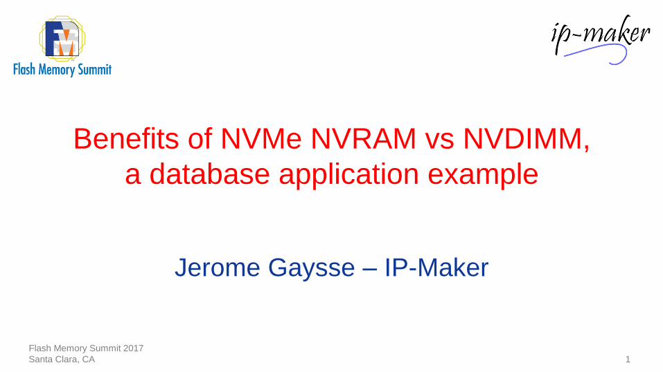
Methodology
Flash Memory Summit 2017
Santa Clara, CA
3
Part 1 - Existing hardware
Flash SSD, NVMe NVRAM, NVDIMM
MS SQL server 2016, HammerDB
Part 2 - Estimation with new product design for higher capacity
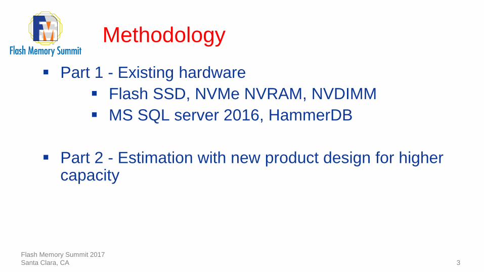
OLTP performance
Flash Memory Summit 2017
Santa Clara, CA
4
A question of latency
Many small read/write accesses to the DB file
Write accesses to the LOG file
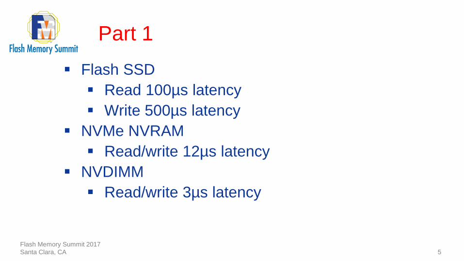
Part 1
Flash Memory Summit 2017
Santa Clara, CA
5
Flash SSD
Read 100µs latency
Write 500µs latency
NVMe NVRAM
Read/write 12µs latency
NVDIMM
Read/write 3µs latency
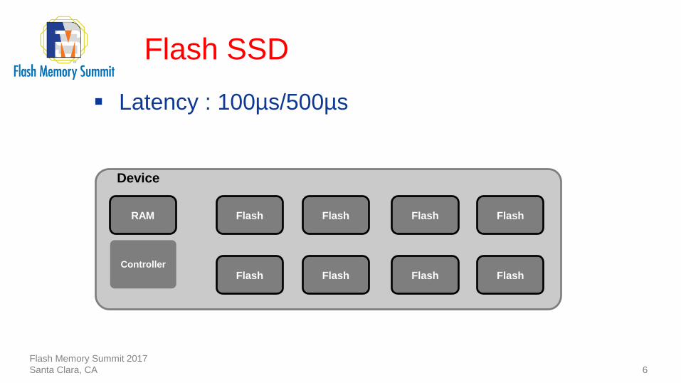
Flash SSD
Flash Memory Summit 2017
Santa Clara, CA
6
Latency : 100µs/500µs
Controller
Device
Flash RAM Flash Flash Flash
Flash Flash Flash Flash

NVMe RAM
Flash Memory Summit 2017
Santa Clara, CA
7
12µs latency
PCIe Interface
IPM-NVMe
DMA DMA DMA
DMA
Automatic Command Processing
Bridge Bridge DDR3
Controller
7-series Xilinx FPGA Host
CPU
DDR
NVMe driver
Device
4GB
DDR3
7-series Xilinx evaluation kit

Latency details
Flash Memory Summit 2017
Santa Clara, CA
8
Gen3x4, FPGA demo, OS IRQ 12µs

Options to reduce latency
Flash Memory Summit 2017
Santa Clara, CA
9
PCIe gen 4
Command Memory Buffer (CMB)
Command Memory Buffer (CMB) with persistent memory
Polling mode
=> from 12 to 5µs

NVMe NVRAM Implementation
(NVDIMM-N like)
Flash Memory Summit 2017
Santa Clara, CA
10
NVDIMM
Flash Memory Summit 2017
Santa Clara, CA
11
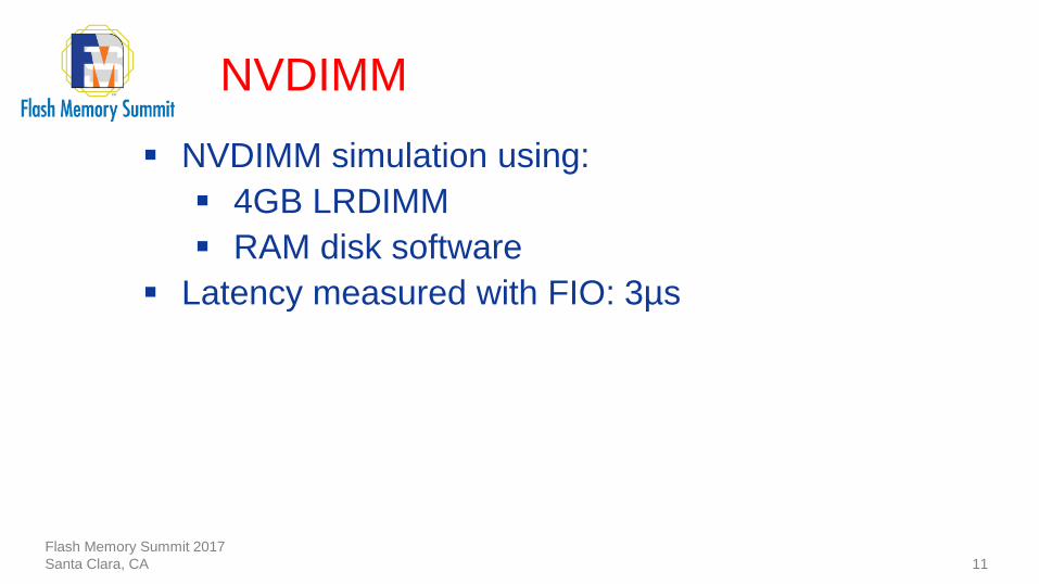
NVDIMM simulation using:
4GB LRDIMM
RAM disk software
Latency measured with FIO: 3µs

Performance results
Flash Memory Summit 2017
Santa Clara, CA
12
5 000
10 000
TPM
Flash
SSD
NVMe
NVRAM
NVDIMM
12µs 3µs 100/500µs
$2/GB
5TB
$30GB
32-64GB
$40/GB
8-16GB

The price for performance
Flash Memory Summit 2017
Santa Clara, CA
13
Flash: $2/GB, 5TB
4K TPM
NVMe NVRAM: $30/GB, 32GB
10K TPM
NVDIMM: $40/GB, 8GB
14K TPM
What about TCO for TB database?

Part 2
Flash Memory Summit 2017
Santa Clara, CA
14
NVMe NVRAM
High storage capacity ?
NVDIMM
High storage capacity ?

NVMe NVRAM Product design
Flash Memory Summit 2017
Santa Clara, CA
15
Achieving high capacity and low write latency
Non-volatile buffer for low latency
Nandflash storage for high capacity
Highly parallel implementation for high throughput
Based on pairs of NVRAM and nandflash memories.
The data is first coming from the controller (1).
Then it is copied in the nandflash (2).
NVRAM
Nandflash
(1) (2)

Theory of operation (1/2)
Flash Memory Summit 2017
Santa Clara, CA
16
The first 4 IOs are sent to the NVRAM buffer 0.
The second 4 IOs are sent to the NVRAM buffer 1.
During this time, the data is read from the NVRAM buffer 0 and written into the nandflash channel 0.

Theory of operation (2/2)
Flash Memory Summit 2017
Santa Clara, CA
17
Copy
4 IOs NVRAM ch0
NVRAM ch1
UNFC ch0
4IOs, IO=4kB, QD=1,
total = 4x 20µs=80µs
Sequence:
1=write to NVRAM CH0
2=write to NVRAM CH1
3=copy from NVRAM to Flash
4=prog flash
…
Prog
16kB@800MB/s=20µs
Prog time = 1200µs
Nandflash Controller
DDR Controller
NandFlash
NVRAM
buffer
Nandflash Controller
DDR Controller
NandFlash
NVRAM
buffer
ch0
ch1
4 IOs
IPM-NVMe

NVMe NVRAM Implementation
(with MRAM)
Flash Memory Summit 2017
Santa Clara, CA
18
SSD Controller
PCIe
IPM-NVMe Nandflash Controller
DMA DMA DMA DMA
Automatic Command Processing
DDR Controller
NandFlash
Channel 0
NVRAM
buffer
Nandflash Controller
DDR Controller
NandFlash
NVRAM
buffer
Channel 15
MRAM
MRAM
20µs latency

NVDIMM
Flash Memory Summit 2017
Santa Clara, CA
19
Higher storage capacity?
Yes, few hundreds of GB of Flash can be added
Highly parallel design?
No, limited by PCB area
Average latency to increase
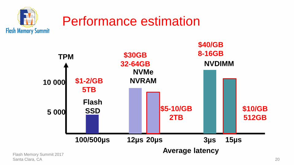
Performance estimation
Flash Memory Summit 2017
Santa Clara, CA
20
5 000
10 000
TPM
Flash
SSD
NVMe
NVRAM
NVDIMM
12µs 3µs 100/500µs 20µs 15µs
Average latency
$1-2/GB
5TB
$5-10/GB
2TB
$30GB
32-64GB
$40/GB
8-16GB
$10/GB
512GB

The price for performance
Flash Memory Summit 2017
Santa Clara, CA
21
Flash: $2/GB, 5TB
4K TPM
NVMe NVRAM: $5/GB, 2TB
9K TPM
NVDIMM: $10/GB, 512GB
13K TPM

Synthesis
Flash Memory Summit 2017
Santa Clara, CA
22
SATA
Flash NVMe
Flash
NV-DIMM
RAM+Flash
$1/GB
$2/GB
$40/GB
TB
IOPS at low queue depth
Capacity Performance
NVMe
NVRAM

NVMe NVRAM vs NVDIMM
Flash Memory Summit 2017
Santa Clara, CA
23 IP-Maker Confidential
23
Log
NVMe
NVRAM NVMe
NVRAM
DB
OLTP application
NVMe NVRAM:
for both Logs and DB files

Flash Memory Summit 2017
Santa Clara, CA
24
Jerome Gaysse
www.ip-maker.com