Embed Size (px)
Citation preview

General DescriptionThe MAX11261 is a 6-channel, 24-bit delta-sigma ADC that achieves exceptional performance while consuming very low power. Sample rates up to 16ksps allow precision DC measurements. The device also features a 64-entry, on-chip FIFO to offload the host processor. The MAX11261 communicates through an I2C-compatible serial interface and is available in a small, wafer-level package (WLP).The MAX11261 offers a 6.2nV/√Hz noise programmable gain amplifier (PGA) with gain settings from 1x to 128x. The integrated PGA provides isolation of the signal inputs from the switched capacitor sampling network. The PGA also enables the MAX11261 to interface directly with high-impedance sources without compromising available dynamic range.The MAX11261 operates from a single 2.7V to 3.6V analog supply. The digital supply range is 1.7V to 2.0V (internal LDO off) and 2.0V to 3.6V (internal LDO on) enabling communication with 1.8V, 2.5V, 3V, or 3.3V logic.
Applications ● Wearable Electronics ● Medical Equipment ● Weigh Scales ● Pressure Sensors ● Battery-Powered Instrumentation
Ordering Information appears at end of data sheet.
19-100250; Rev 0; 2/18
Benefits and Features ● Analog Supply
• 2.7V to 3.6V ● Digital Supply
• Internal LDO Disabled—1.7V to 2.0V• Internal LDO Enabled—2.0V to 3.6V
● 3ppm INL (typ) ● PGA
• Gains of 1, 2, 4, 8, 16, 32, 64, 128• Low-Noise Mode, 6.2nV/√Hz Noise• Low-Power Mode, 10nV/√Hz Noise
● Input-Referred Noise• PGA Low-Noise Mode, Gain of 64 at 1ksps
Continuous, 0.15μVRMS ● Fully Differential Signal and Reference Inputs ● Internal System Clock of 8.192MHz ● I2C-Compatible Serial Interface ● Supports Standard, Fast-Mode, and Fast-Mode Plus
I2C Specifications ● 64-Entry On-Chip FIFO ● Hardware Interrupt for Input Monitoring and FIFO
Usage ● On-Demand Self and System Gain and Offset
Calibration ● User-Programmable Offset and Gain Registers ● Two Power-Down Modes (SLEEP and STANDBY) ● Low Power Dissipation ● ESD Rating: ±2.5kV (HBM), 750V (CDM) ● -40°C to +85°C Operating Temperature Range ● Wafer-Level Package (WLP) (6 x 6 Bump, 0.4mm
Pitch, 2.838mm x 2.838mm x 0.5mm)
MAX11261 24-Bit, 6-Channel, 16ksps, 6.2nV/√Hz PGA, Delta-Sigma ADC with I2C Interface
EVALUATION KIT AVAILABLE

Typical Application Circuit
MAX11261µC
1nFC0G
AIN5P
AIN5NGPO0
1nFC0G
GPO5
AIN0N
AIN0P
10nF
REFN REFP
1µF
AVDD
2.7V TO 3.6V
GPOGND CAPP CAPN
1nFC0G
CAPREG
220nF0603 X7R
DGNDAVSS
RDYB_INTB
SDA
ADR1
SCL
ADR0
1µF
RESISTIVE BRIDGE MEASUREMENT CIRCUIT, I2C CONFIGURATION
DVDD
2.0V TO 3.6V
REF
RSTB
SYNC
www.maximintegrated.com Maxim Integrated │ 2
MAX11261 24-Bit, 6-Channel, 16ksps, 6.2nV/√Hz PGA, Delta-Sigma ADC with I2C Interface

AVDD to AVSS .....................................................-0.3V to +3.9VDVDD to DGND ....................................................-0.3V to +3.9VAVSS to DGND ....................................................-0.3V to +0.3VAnalog Inputs:GPOGND to AVSS or DGND ...............................-0.3V to +0.3V(AIN_P, AIN_N, CAPP, CAPN, REFP, REFN) to AVSS ..... -0.3V to
the lower of +3.9V or (VAVDD + 0.3V)GPO_ to GPOGND or AVSS or DGND ...... -0.3V to the lower of
+3.9V or (VAVDD + 0.3V)Digital Inputs:(RSTB, SYNC, SCL, SDA, ADR0, ADR1) to DGND .......... -0.3V to
the lower of +3.9V or (VDVDD + 0.3V)Digital Outputs:(RDYB_INTB, SDA, SYNC) to DGND ............................ -0.3V to
(VDVDD + 0.3V)
CAPREG to DGND ...............................................-0.3V to +2.1VMaximum Continuous Current into Any Pins Except GPO_
and GPOGND Pins.......................................................±50mAMaximum Continuous Current into GPO_
and GPOGND Pins.......................................................150mAContinuous Power Dissipation (TA = +70°C; WLP;
derate 21.7mW/°C above +70°C) ..............................1736mWOperating Temperature Range ........................... -40°C to +85°CJunction Temperature ......................................................+150°CStorage Temperature Range ............................ -55°C to +150°CSoldering Temperature (reflow) .......................................+260°C
36 WLPPACKAGE CODE N362B2+2
Outline Number 21-0742Land Pattern Number Refer to Application Note 1891Thermal Resistance, Four-Layer Board:Junction to Ambient (θJA) 46 °C/WJunction to Case (θJC) N/A
Absolute Maximum Ratings
Stresses beyond those listed under “Absolute Maximum Ratings” may cause permanent damage to the device. These are stress ratings only, and functional operation of the device at these or any other conditions beyond those indicated in the operational sections of the specifications is not implied. Exposure to absolute maximum rating conditions for extended periods may affect device reliability.
Package thermal resistances were obtained using the method described in JEDEC specification JESD51-7, using a four-layer board. For detailed information on package thermal considerations, refer to www.maximintegrated.com/thermal-tutorial.
For the latest package outline information and land patterns (footprints), go to www.maximintegrated.com/packages. Note that a “+”, “#”, or “-” in the package code indicates RoHS status only. Package drawings may show a different suffix character, but the drawing pertains to the package regardless of RoHS status.
Package Information
www.maximintegrated.com Maxim Integrated │ 3
MAX11261 24-Bit, 6-Channel, 16ksps, 6.2nV/√Hz PGA, Delta-Sigma ADC with I2C Interface

(VAVDD = 3.6V, VAVSS = 0V, VDVDD = 2.0V to 3.6V, VREFP - VREFN = VAVDD, DATA RATE = 1ksps, PGA low-noise mode, single-cycle conversion mode (SCYCLE = 1). TA = TMIN to TMAX, unless otherwise noted. Typical values are at TA = +25°C.)(Note 1 )
PARAMETER SYMBOL CONDITIONS MIN TYP MAX UNITSSTATIC PERFORMANCE (Single-Cycle Conversion Mode)
Noise Voltage (Referred to Input) Vn
PGA gain of 128, single-cycle mode at 1ksps data rate
PGA low-noise mode 0.19
μVRMS
PGA low-power mode 0.26
PGA gain of 128, single-cycle mode at 12.8ksps data rate
PGA low-noise mode 0.83PGA low-power mode 1.16
PGA gain of 128, continuous mode at 64ksps data rate
PGA low-noise mode 0.83PGA low-power mode 1.16
Integral Nonlinearity INL 3 15 ppmZero Error ZERR After system zero-scale calibration 1 μVZero Drift ZDrift 50 nV/°CFull-Scale Error (Notes 2 and 3) FSE After system full-scale calibration 2 ppmFSRFull-Scale Error Drift FSEDrift 0.05 ppmFSR/°C
Common-Mode Rejection CMRDC rejection 110 130
dB50Hz/60Hz rejection (Note 4) 110 130DC rejection with PGA gain 128 80 95
AVDD, AVSS DC Supply Rejection Ratio PSRRA
DC rejection 75 95dB50Hz/60Hz rejection (Note 4) 75 95
DC rejection with PGA gain 128 65 75
DVDD DC Supply Rejection Ratio PSRRD
DC rejection 103 115dB50Hz/60Hz rejection (Note 4) 103 115
DC rejection with PGA gain 128 86 110PGAGain Setting 1 128 V/V
Noise-Spectral Density NSDLow-noise mode 6.2
nV/√HzLow-power mode 10
Gain Error, Not Calibrated GERR
Gain = 1 0.75
%
Gain = 2 1.2Gain = 4 2Gain = 8 3Gain = 16 4.5Gain = 32 6Gain = 64 5.5Gain = 128 2
Output Voltage Range VOUTRNGVAVSS + 0.3
VAVDD - 0.3 V
Electrical Characteristics
www.maximintegrated.com Maxim Integrated │ 4
MAX11261 24-Bit, 6-Channel, 16ksps, 6.2nV/√Hz PGA, Delta-Sigma ADC with I2C Interface

(VAVDD = 3.6V, VAVSS = 0V, VDVDD = 2.0V to 3.6V, VREFP - VREFN = VAVDD, DATA RATE = 1ksps, PGA low-noise mode, single-cycle conversion mode (SCYCLE = 1). TA = TMIN to TMAX, unless otherwise noted. Typical values are at TA = +25°C.)(Note 1 )
PARAMETER SYMBOL CONDITIONS MIN TYP MAX UNITSMUXChannel-to-Channel Isolation ISOCH-CH DC 140 dBGENERAL-PURPOSE OUTPUTS
Resistance (On) RONVoltage between GPO_ and GPOGND < 200mV, GPOGND connected to AVSS 3.5 10 Ω
Maximum Current (On) IMAX
Per output 30mATotal from all outputs into GPOGND bump
(Note 4) 90
Leakage Current (Off)Ileak1
Current into the GPOGND pin with one individual GPO_ pin connected to 3V 0.4
nAIleak6
Current into the GPOGND pin with all GPO_ pins connected to 3V 13 100
AUTOSCAN TIMERTimer Resolution ASTRES 4 msAccuracy ASTACC Over voltage and temperature (Note 4) 5 10 %POWER-UP DELAYS (Note 4)
Power-Up TimeTPUPSLP
SLEEP state (full power-down) to LDO wake-up, VAVDD = 2.7V, VDVDD = 2.0V, CAPREG = 220nF
23 45μs
TPUPSBYSTANDBY state (analog blocks powered down, LDO on) to Active 4 8
RSTB Fall to RDYB ‘1’ tR2RDYB transition from ‘0’ to ‘1’ on falling edge of RSTB (Note 4) 300 ns
ANALOG INPUTS/REFERENCE INPUTS
Common-Mode Input Voltage Range, VCM = (VAIN_P + VAIN_N)/2
CMIRNG
Direct (PGA bypassed) VAVSS VAVDDV
PGA VAVSS + 0.3
VAVDD -1.3
Absolute Input Voltage RangeVABSRNG Direct (PGA bypassed) VAVSS VAVDD
VVABSRNG PGA VAVSS
+ 0.3VAVDD
-1.3DC Input Leakage IINLEAK SLEEP state enabled ±0.1 nADifferential Input Conductance GDIFF Direct (PGA bypassed) ±11.6 μA/VDifferential Input Current IDIFF PGA enabled ±1.0 nACommon-Mode Input Conductance GCM Direct (PGA bypassed) ±1.0 μA/VCommon-Mode Input Current ICM PGA enabled ±10 nAReference Differential Input Resistance RREF Active state 26 kΩ
Reference Differential Input Current IREF_PD STANDBY and SLEEP state ±1 nA
Electrical Characteristics (continued)
www.maximintegrated.com Maxim Integrated │ 5
MAX11261 24-Bit, 6-Channel, 16ksps, 6.2nV/√Hz PGA, Delta-Sigma ADC with I2C Interface

(VAVDD = 3.6V, VAVSS = 0V, VDVDD = 2.0V to 3.6V, VREFP - VREFN = VAVDD, DATA RATE = 1ksps, PGA low-noise mode, single-cycle conversion mode (SCYCLE = 1). TA = TMIN to TMAX, unless otherwise noted. Typical values are at TA = +25°C.)(Note 1 )
PARAMETER SYMBOL CONDITIONS MIN TYP MAX UNITS
Input CapacitanceCIN Direct (PGA bypassed) 2.5
pFCPGAIN PGA 0.25
Voltage Range (AINP - AINN) VIN(DIFF)Unipolar 0 VREF VBipolar -VREF +VREF
AINP, AINN Sampling Rate fS 4.096 MHzREFP, REFN Voltage Range VRABSRNG (Note 5) VAVDD VREFP – REFN Differential Voltage Range VREF 1.5 VAVDD V
REFP, REFN Sampling Rate 4.096 MHzSENSOR FAULT DETECT CURRENTSCurrent 1.1 μAInitial Tolerance ±10 %Drift 0.3 %/°CDIGITAL SINC FILTER RESPONSE
Bandwidth (-3dB)0.203
x DATA RATE
Hz
Settling Time (Latency) 5/DATA RATE s
LOGIC INPUTSVIMAX_I2C Maximum input voltage of SDA and SCL VDVDD VInput Current IDIGILEAK Leakage current ±1 μA
Input Low Voltage VIL0.3 x
VDVDDV
Input High Voltage VIH0.7 x
VDVDDV
Input Hysteresis VHYS 200 mVLOGIC OUTPUTSVOMAX_I2C Maximum output voltage of SDA VDVDD VOutput Low Level VOL IOL = 1mA 0.4 VOutput High Level (RDYB, DOUT) VOH IOH = 1mA 0.9 x
VDVDDV
Floating State Leakage Current IDIGOLEAK ±10 μAFloating State Output Capacitance CDIGO 9 pF
Electrical Characteristics (continued)
www.maximintegrated.com Maxim Integrated │ 6
MAX11261 24-Bit, 6-Channel, 16ksps, 6.2nV/√Hz PGA, Delta-Sigma ADC with I2C Interface

(VAVDD = 3.6V, VAVSS = 0V, VDVDD = 2.0V to 3.6V, VREFP - VREFN = VAVDD, DATA RATE = 1ksps, PGA low-noise mode, single-cycle conversion mode (SCYCLE = 1). TA = TMIN to TMAX, unless otherwise noted. Typical values are at TA = +25°C.)(Note 1 )
PARAMETER SYMBOL CONDITIONS MIN TYP MAX UNITSPOWER REQUIREMENTSNegative Analog Supply Voltage VAVSS 0 VPositive Analog Supply Voltage VAVDD 2.7 3.6 V
I/O Supply Voltage VDVDD
CAPREG is not being driven by external supply 2.0 3.6
VDVDD and CAPREG bumps connected together on the circuit board 1.7 2.0
CAPREG Supply Voltage VCAPREG
Voltage developed internally from DVDD using a subregulator; When CAPREG pin is driven externally, ensure that it is connected directly to DVDD pin.
1.7 2.0 V
Analog Supply Current IAVDD
Direct 2.2 3mAPGA low-power mode 3.5 4.6
PGA low-noise mode 4.2 5.65
DVDD Operating Current IDVDD(CNV)VDVDD = 2.0V, LDO enabled 0.65 1.1
mAVDVDD = VCAPREG = 2.0V, LDO disabled 0.58
AVDD Sleep Current IAVDD(SLP)VAVDD = 3.466V, VAVSS = 0V, VDVDD = 2.0V 1 μA
DVDD Sleep Current IDVDD(SLP) VDVDD = 2.0V 0.3 1 μA
AVDD Standby Current IAVDD(SBY)VAVDD = 3.465V, VAVSS = 0V, VDVDD = 2.0V 1.5 μA
DVDD Standby Current IDVDD(SBY)VDVDD = 2.0V, LDO enabled 50 175
μAVDVDD = VCAPREG = 2.0V, LDO disabled 2.5
UVLO Threshold Low-to-High VLHAVDD, DVDD supply undervoltage lockout 0.8 1.2 1.65
VCAPREG supply undervoltage lockout 0.7 1.0 1.35
UVLO Threshold High-to-Low VHLAVDD, DVDD supply undervoltage lockout 0.6 1.1 1.5
VCAPREG supply undervoltage lockout 0.5 0.95 1.3
UVLO Hysteresis VHYSAVDD, DVDD supply undervoltage lockout 4
%CAPREG supply undervoltage lockout 5
UVLO Delay Low-to-High or High-to-Low TDEL
AVDD, DVDD supply undervoltage lockout 10μs
CAPREG supply undervoltage lockout 3.5
UVLO Glitch Suppression TPAVDD, DVDD supply undervoltage lockout 10
nsCAPREG supply undervoltage lockout 10
Electrical Characteristics (continued)
www.maximintegrated.com Maxim Integrated │ 7
MAX11261 24-Bit, 6-Channel, 16ksps, 6.2nV/√Hz PGA, Delta-Sigma ADC with I2C Interface

Note 1: Limits are 100% tested at TA = +25°C, unless otherwise noted. Limits over the operating temperature range and relevant supply voltage range are guaranteed by design and characterization.
Note 2: Full-scale error includes errors from gain and offset or zero-scale error.Note 3: ppmFSR is parts per million of full-scale range.Note 4: These specifications are guaranteed by design, characterization, or I2C protocol.Note 5: Reference common mode (VREFP + VREFN)/2 ≤ (VAVDD + VAVSS)/2 + 0.1V.
PARAMETER SYMBOL CONDITIONS MIN TYP MAX UNITSSerial Clock Frequency fSCL Note 4 applies to minimum value 0.1 1 MHzBus Free Time Between STOP and START Condition tBUF 0.5 μs
Hold Time (Repeated) START Condition (After This Period, First Clock Pulse Is Generated)
tHD;STA 0.26 μs
SCL Pulse-Width Low tLOW 0.5 μsSCL Pulse-Width High tHIGH 0.26 μsSetup Time for Repeated START Condition tSU;STA 0.26 μs
Data Hold Time tHD;DAT 0 μsData Setup Time tSU;DAT 50 nsSDA and SCL Receiving Rise Time tr (Note 4) 120 ns
SDA and SCL Receiving Fall Time tf (Note 4) 20 x
VDVDD/5.5 120 ns
SDA Transmitting Fall Time tf 20 x VDVDD/5.5 120 ns
Setup Time for STOP Condition tSU;STO 0.26 μsBus Capacitance Allowed Cb (Note 4) 550 pFPulse Width of Suppressed Spike tSP 50 ns
Figure 1. I2C Timing Diagram
I2C Timing Requirements
SDA
SCL
tBUF
tSU;STO
t rtSPtHD;STA
tSU;STA
tf
t HIGH
tSU;DAT
tHD;DAT
trtLOW
tHD;STA
tf
S SSr P
www.maximintegrated.com Maxim Integrated │ 8
MAX11261 24-Bit, 6-Channel, 16ksps, 6.2nV/√Hz PGA, Delta-Sigma ADC with I2C Interface

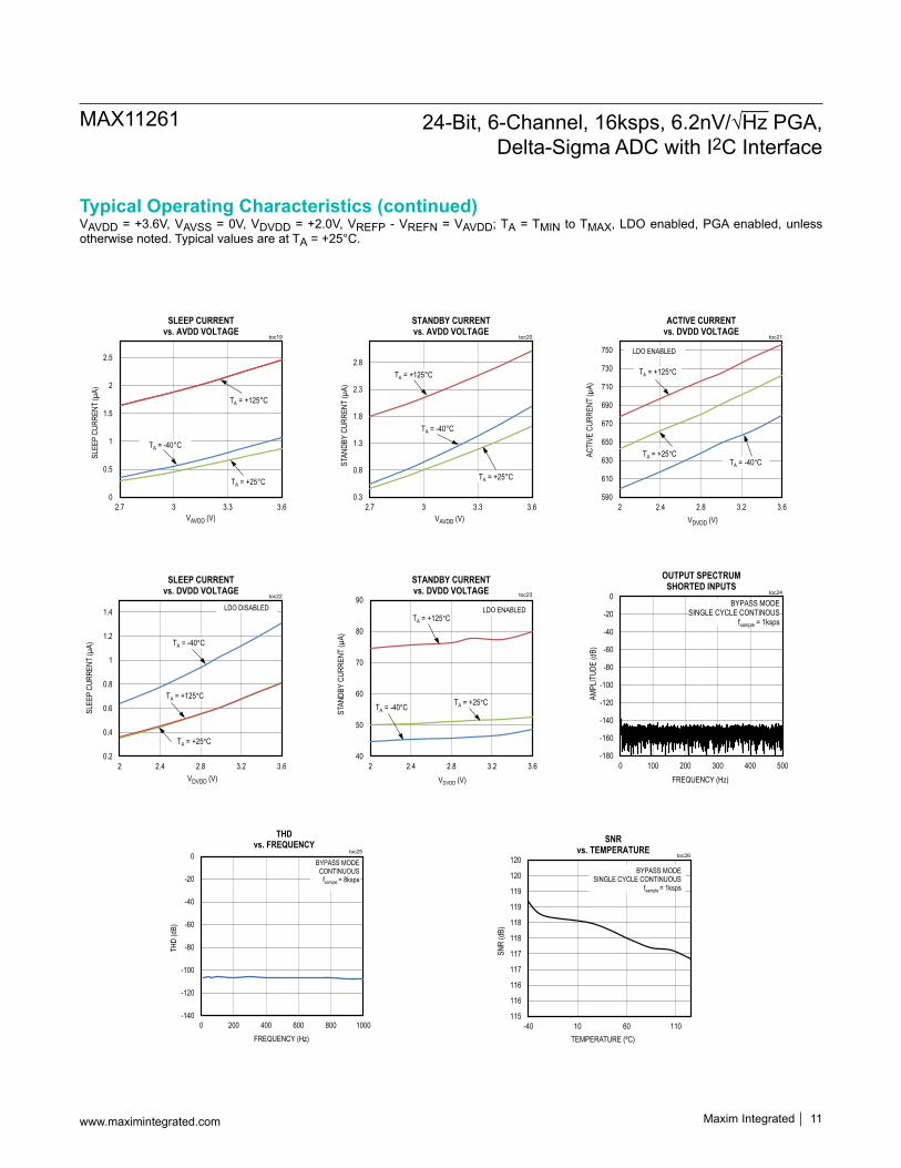
VAVDD = +3.6V, VAVSS = 0V, VDVDD = +2.0V, VREFP - VREFN = VAVDD; TA = TMIN to TMAX, LDO enabled, PGA enabled, unless otherwise noted. Typical values are at TA = +25°C.
Typical Operating Characteristics
-5
-4
-3
-2
-1
0
1
2
3
4
5
-3.5 -2.5 -1.5 -0.5 0.5 1.5 2.5 3.5
INL
(ppm
)
DIFFERENTIAL INPUT (V)
INL vs. INPUT VOLTAGE
TA = +25°C
toc01
BYPASS MODE
TA = -40°C
TA = +125°C
0.0
0.1
0.2
0.3
0.4
0.5
-50 0 50 100 150
NO
ISE
(µV R
MS)
TEMPERATURE (°C)
INPUT-REFERRED NOISE vs. TEMPERATURE
toc04
PGA GAIN = 128V/V
-5
-4
-3
-2
-1
0
1
2
3
4
5
-3.5 -2.5 -1.5 -0.5 0.5 1.5 2.5 3.5
INL
(ppm
)
DIFFERENTIAL INPUT (V)
INL vs. INPUT VOLTAGE
TA = +25°C
toc02
PGA GAIN = 4V/V
TA = -40°C
TA = +125°C
-25
-20
-15
-10
-5
0
-40 -25 -10 5 20 35 50 65 80 95 110 125
OFF
SET
ERR
OR
(LSB
)
TEMPERATURE (°C)
OFFSET ERRORvs. TEMPERATURE
toc05
BYPASS MODE
PGA = 4
0.00
0.10
0.20
0.30
0.40
0.50
0 0.5 1 1.5 2 2.5
NO
ISE
(µV R
MS)
COMMON-MODE VOLTAGE (V)
INPUT-REFERRED NOISE vs. COMMON-MODE VOLTAGE
toc03
PGA GAIN = 128V/V
TA = +25°C
TA = -40°C
TA = +125°C
-20
-15
-10
-5
0
5
2.7 3 3.3 3.6
OFF
SET
ERR
OR
(LSB
)
VAVDD (V)
OFFSET ERRORvs. AVDD VOLTAGE
toc06
TA = +125°C
TA = -40°C
TA = +25°C
BYPASS MODE
-28
-23
-18
-13
-8
2.7 3 3.3 3.6
OFF
SET
ERR
OR
(LSB
)
VAVDD (V)
OFFSET ERRORvs. AVDD VOLTAGE
toc07
TA = +125°C
TA = -40°C
TA = +25°C
PGA = 4
-50
-40
-30
-20
-10
0
10
1.5 2.2 2.9 3.6
OFF
SET
ERR
OR
(LSB
)
VREFP - VREFN (V)
OFFSET ERRORvs. VREFP - VREFN toc08
BYPASS MODE
TA = +125°C
TA = +25°C
TA = -40°C
-55
-45
-35
-25
-15
-5
5
1.5 2.2 2.9 3.6
OFF
SET
ERR
OR
(LSB
)
VREFP - VREFN (V)
OFFSET ERRORvs. VREFP - VREFN toc09
PGA = 4
TA = +25°C
TA = +125°C
TA = -40°C
Maxim Integrated │ 9www.maximintegrated.com
MAX11261 24-Bit, 6-Channel, 16ksps, 6.2nV/√Hz PGA, Delta-Sigma ADC with I2C Interface

VAVDD = +3.6V, VAVSS = 0V, VDVDD = +2.0V, VREFP - VREFN = VAVDD; TA = TMIN to TMAX, LDO enabled, PGA enabled, unless otherwise noted. Typical values are at TA = +25°C.
Typical Operating Characteristics (continued)
8.0
8.1
8.1
8.2
8.2
8.3
8.3
8.4
8.4
8.5
8.5
-40 -25 -10 5 20 35 50 65 80 95 110 125
FREQ
UEN
CY
(MH
z)
TEMPERATURE (°C)
INTERNAL OSCILLATOR FREQUENCYvs. TEMPERATURE
toc10
-120
-115
-110
-105
-100
-95
-90
-85
10 100 1000 10000 100000 1000000
PSR
R (d
B)
FREQUENCY ON AVDD (Hz)
PSRRvs. FREQUENCY ON AVDD
fsample = 12.8kspsBYPASS MODE
VAVDD = 3.3V ±50mVP-P
toc13
TA = -40°C
TA = +25°C
TA = +125°C
8.16
8.17
8.17
8.18
8.18
8.19
8.19
8.20
8.20
1.7 1.8 1.9 2
FREQ
UEN
CY
(MH
z)
VDVDD (V)
INTERNAL OSCILLATOR FREQUENCYvs. DVDD VOLTAGE
toc11
LDO DISABLED
-130
-125
-120
-115
-110
-105
-100
10 100 1000 10000 100000 1000000
PSR
R (d
B)
FREQUENCY ON DVDD (Hz)
PSRRvs. FREQUENCY ON DVDD
fsample = 12.8kspsBypass Mode
VDVDD = 2.1V ±50mVP-P
toc14
TA = -40°C
TA = +25°C
TA = +125°C
8.16
8.17
8.17
8.18
8.18
8.19
8.19
8.20
8.20
2 2.5 3 3.5
FREQ
UEN
CY
(MH
z)
VDVDD (V)
INTERNAL OSCILLATOR FREQUENCYvs. DVDD VOLTAGE
toc12
LDO ENABLED
-0.5
0.5
1.5
2.5
3.5
4.5
5.5
-40 -25 -10 5 20 35 50 65 80 95 110 125
ACTI
VE C
UR
REN
T (m
A)
TEMPERATURE (°C)
ACTIVE CURRENTvs. TEMPERATURE
toc15
PGA LOW NOISE
IDVDD
IAVDD
0
0.5
1
1.5
2
2.5
3
-40 -25 -10 5 20 35 50 65 80 95 110 125
SLEE
P C
UR
REN
T (µ
A)
TEMPERATURE (°C)
SLEEP CURRENTvs. TEMPERATURE
toc16
IDVDD_SLEEP
IAVDD_SLEEP
1
10
100
-40 -25 -10 5 20 35 50 65 80 95 110 125
STAN
DBY
CU
RR
ENT
(µA)
TEMPERATURE (°C)
IAVDD_STBY
STANDBY CURRENTvs. TEMPERATURE
toc17
IDVDD_STBY
3
3.5
4
4.5
5
5.5
6
2.7 3 3.3 3.6
ACTI
VE C
UR
REN
T (m
A)
VAVDD (V)
ACTIVE CURRENTvs. AVDD VOLTAGE
toc18
PGA LOW NOISE
TA = +25°CTA = -40°C
TA = +125°C
Maxim Integrated │ 10www.maximintegrated.com
MAX11261 24-Bit, 6-Channel, 16ksps, 6.2nV/√Hz PGA, Delta-Sigma ADC with I2C Interface
VAVDD = +3.6V, VAVSS = 0V, VDVDD = +2.0V, VREFP - VREFN = VAVDD; TA = TMIN to TMAX, LDO enabled, PGA enabled, unless otherwise noted. Typical values are at TA = +25°C.
Typical Operating Characteristics (continued)
0
0.5
1
1.5
2
2.5
2.7 3 3.3 3.6
SLEE
P C
UR
REN
T (µ
A)
VAVDD (V)
SLEEP CURRENTvs. AVDD VOLTAGE
toc19
TA = -40°C
TA = +125°C
TA = +25°C
0.2
0.4
0.6
0.8
1
1.2
1.4
2 2.4 2.8 3.2 3.6
SLEE
P C
UR
REN
T (µ
A)
VDVDD (V)
SLEEP CURRENTvs. DVDD VOLTAGE
toc22
LDO DISABLED
TA = -40°C
TA = +25°C
TA = +125°C
0.3
0.8
1.3
1.8
2.3
2.8
2.7 3 3.3 3.6
STAN
DBY
CU
RR
ENT
(µA)
VAVDD (V)
STANDBY CURRENTvs. AVDD VOLTAGE
toc20
TA = -40°C
TA = +125°C
TA = +25°C
40
50
60
70
80
90
2 2.4 2.8 3.2 3.6
STAN
DBY
CU
RR
ENT
(µA)
VDVDD (V)
STANDBY CURRENTvs. DVDD VOLTAGE toc23
LDO ENABLED
TA = -40°C TA = +25°C
TA = +125°C
590
610
630
650
670
690
710
730
750
2 2.4 2.8 3.2 3.6
ACTI
VE C
UR
REN
T (µ
A)
VDVDD (V)
ACTIVE CURRENTvs. DVDD VOLTAGE
toc21
LDO ENABLED
TA = -40°CTA = +25°C
TA = +125°C
-180
-160
-140
-120
-100
-80
-60
-40
-20
0
0 100 200 300 400 500
AMPL
ITU
DE
(dB)
FREQUENCY (Hz)
OUTPUT SPECTRUMSHORTED INPUTS
BYPASS MODESINGLE CYCLE CONTINOUS
fsample = 1ksps
toc24
-140
-120
-100
-80
-60
-40
-20
0
0 200 400 600 800 1000
THD
(dB)
FREQUENCY (Hz)
THDvs. FREQUENCY
toc25
BYPASS MODECONTINUOUS
fsample = 8ksps
115
116
116
117
117
118
118
119
119
120
120
-40 10 60 110
SNR
(dB)
TEMPERATURE (ºC)
SNRvs. TEMPERATURE
toc26
BYPASS MODESINGLE CYCLE CONTINUOUS
fsample = 1ksps
Maxim Integrated │ 11www.maximintegrated.com
MAX11261 24-Bit, 6-Channel, 16ksps, 6.2nV/√Hz PGA, Delta-Sigma ADC with I2C Interface

PIN NAME FUNCTION TYPE
A1 AIN0P Positive Analog Input 0. A 1nF C0G capacitor should be added between differential input pin pairs. IN/Analog
A2 AIN1P Positive Analog Input 1. A 1nF C0G capacitor should be added between differential input pin pairs. IN/Analog
A3 AIN2P Positive Analog Input 2. A 1nF C0G capacitor should be added between differential input pin pairs. IN/Analog
A4 AIN3P Positive Analog Input 3. A 1nF C0G capacitor should be added between differential input pin pairs. IN/Analog
A5 AIN4P Positive Analog Input 4. A 1nF C0G capacitor should be added between differential input pin pairs. IN/Analog
A6 AIN5P Positive Analog Input 5. A 1nF C0G capacitor should be added between differential input pin pairs. IN/Analog
B1 AIN0N Negative Analog Input 0 IN/AnalogB2 AIN1N Negative Analog Input 1 IN/AnalogB3 AIN2N Negative Analog Input 2 IN/AnalogB4 AIN3N Negative Analog Input 3 IN/Analog
Bump Configuration
MAX11261
TOP VIEW(BUMP SIDE DOWN)
A
B
C
D
E
F
1
+
AIN0P AIN1P AIN2P AIN3P AIN4P AIN5P
2 3 4 5 6
AIN0N AIN1N AIN2N AIN3N AIN4N AIN5N
AVSS REFP REFN CAPN CAPP AVSS
AVDD GPO0 SYNC GPO4 RSTBGPOGND
RDYB_INTB
SDA ADR0 GPO1 GPO2 GPO3
SCL GPO5 ADR1 DGNDCAPREG
DVDD
WLP 6 x 6 0.4mm PITCH
0.5mm HEIGHT
Bump Descriptions
www.maximintegrated.com Maxim Integrated │ 12
MAX11261 24-Bit, 6-Channel, 16ksps, 6.2nV/√Hz PGA, Delta-Sigma ADC with I2C Interface

PIN NAME FUNCTION TYPEB5 AIN4N Negative Analog Input 4 IN/AnalogB6 AIN5N Negative Analog Input 5 IN/Analog
C1, C6 AVSS Analog Ground AGNDC2 REFP Positive Reference Input IN/AnalogC3 REFN Negative Reference Input IN/AnalogC4 CAPN PGA Filter Input. Connect 1nF C0G capacitor between CAPP and CAPN. IN/AnalogC5 CAPP PGA Filter Input. Connect 1nF C0G capacitor between CAPP and CAPN. IN/AnalogD1 AVDD Positive Analog Supply PWR
D2 GPO0 Analog Switch Normally Open Terminal/General-Purpose Output 0. Register controlled, close position connects GPO0 to GPOGND. Current sink only. OUT/Analog
D3 SYNC
Synchronization Pin for Multiple Devices. At power-up, the device is default to a master (CTRL3:SYNC = 1) and the SYNC pin output is in high impedance state (CTRL3:SYNCZ = 1). When the device is configured as a master and the register CTRL3:SYNCZ is set to 0, the SYNC pin is changed to an active-low, open-drain output pin. Set CTRL:SYNC to 0 puts the device in salve mode and the SYNC pin is an input. An external pullup resistor is required if the SYNC function is used.
IN/OUT/Digital
D4 GPO4 Analog Switch Normally Open Terminal/General-Purpose Output 4. Register controlled, close position connects GPO4 to GPOGND. Current sink only. OUT/Analog
D5 RSTB Active-Low Power-On-Reset Input IN/DigitalD6 GPOGND Analog Switch/General-Purpose Output, GND Terminal OUT/Analog
E1 RDYB_INTB
Active-Low Open-Drain Output. A pullup resistor to DVDD is required. The typical resistor value is 10kΩ.In sequencer modes 1, 2, and 3: RDYB_INTB goes low when a new conversion result is available in the FIFO. When the FIFO entries are completely read out, RDYB_INTB returns high if no FIFO usage interrupts is asserted. The RDYB_INTB also goes low when there is at least one FIFO usage interrupt.In sequencer mode 4: RDYB_INTB indicates the input comparison result and FIFO usage interrupt.
OUT/Digital
E2 SDA I2C Serial Data IN/OUT/I2CE3 ADR0 I2C Address Select Line 0 IN/Digital
E4 GPO1 Analog Switch Normally Open Terminal/General-Purpose Output 1. Register controlled, close position connects GPO1 to GPOGND. Current sink only. OUT/Analog
E5 GPO2 Analog Switch Normally Open Terminal/General-Purpose Output 2. Register controlled, close position connects GPO2 to GPOGND. Current sink only. OUT/Analog
E6 GPO3 Analog Switch Normally Open Terminal/General-Purpose Output 3. Register controlled, close position connects GPO3 to GPOGND. Current sink only. OUT/Analog
F1 SCL I2C Serial Clock Input IN/Digital/I2C
F2 GPO5 Analog Switch Normally Open Terminal/General-Purpose Output 5. Register controlled, close position connects GPO5 to GPOGND. Current sink only. OUT/Digital
F3 ADR1 I2C Address Select Line 1 INDigitalF4 DGND Digital Ground DGND
F5 CAPREG 1.8V Subregulator Output. Connects to DVDD when driven externally by a 1.8V supply. Connect a 220nF to DGND. PWR
F6 DVDD Digital Power Supply PWR
Pin Description (continued)
www.maximintegrated.com Maxim Integrated │ 13
MAX11261 24-Bit, 6-Channel, 16ksps, 6.2nV/√Hz PGA, Delta-Sigma ADC with I2C Interface

Detailed DescriptionThe MAX11261 is a 24-bit, delta-sigma ADC that achieves exceptional performance consuming minimal power. Sample rates up to 16ksps support precision DC measurements. The built-in sequencer supports scanning of selected analog channels, auto wake-up, programmable conversion delay, and math operations to automate sensor monitoring.The fourth-order, delta-sigma modulator is unconditionally stable and measures the six differential input voltages. To prevent overdriving, the modulator is monitored for over-range conditions and is reported in the status register. The digital filter is a variable decimation-rate SINC filter with overflow monitoring reported in the status register.The programmable gain differential amplifier (PGA) is low noise and is programmable from 1 to 128. The PGA buffers the modulator and provides a high-impedance input to the analog channels.The device stores the conversion results in a 64-entry FIFO. The FIFO interrupts wake up the host processor less frequently to reduce the system power consumption. The device also features an autonomous scan mode to
monitor the inputs activity. The device only interrupts the host when the input is out of a configured range.
System ClockThe MAX11261 incorporates a highly stable internal oscillator that provides the system clock. The system clock is trimmed to 8.192MHz, providing digital and analog timing.
Voltage Reference InputsThe MAX11261 provides differential inputs REFP and REFN for an external reference voltage. Connect the external reference directly across the REFP and REFN bumps to obtain the differential reference voltage. The VREFP voltage should always be greater than the VREFN voltage, and the common-mode voltage range is between 0.75V and VAVDD - 0.75V.
Analog InputsThe MAX11261 measures six pairs of differential analog inputs (AIN_P, AIN_N) in direct connection or buffered through the PGA. See the CTRL2: Control Register 2 (Read/Write) table for programming and enabling the PGA or direct connect mode. The default configuration is direct connect, with the PGA powered down.
Functional Diagrams
TIMINGCLOCK
GENERATOR
DELTA-SIGMAADC
DIGITAL FILTER
SERIAL INTERFACEMUX PGA
AIN0N
AIN0P
AIN5N
AIN5P
AVSS
AVDD
GPOGND
CAPN REFP REFN
1µA
AVDD
1µA
AVSS
DGND
DVDD
GPO0 GPO5
64-ENTRY FIFO
1.8V REGULATOR
CAPREGCAPP
RDYB_INTB
SDA
SCL
ADR1
ADR0
RSTBHIGH-PASS FILTER, TRIP
COMPARATOR
SYNC
www.maximintegrated.com Maxim Integrated │ 14
MAX11261 24-Bit, 6-Channel, 16ksps, 6.2nV/√Hz PGA, Delta-Sigma ADC with I2C Interface

Bypass/Direct ConnectThe MAX11261 offers the option to bypass the PGA and route the analog inputs directly to the modulator. This option lowers the power of the device since the PGA is powered down.
Programmable Gain Amplifier (PGA)The integrated PGA provides gain settings from 1x to 128x (Figure 2). Direct connection is available to bypass the PGA and directly connect to the modulator. The PGA’s absolute input voltage range is CMIRNG and the PGA output voltage range is VOUTRNG, as specified in the Electrical Characteristics.
Note that linearity and performance degrade when the specified input common-mode voltage of the PGA is exceeded. The input common-mode range and output common-mode range are shown in Figure 3. The following equations describe the relationship between the analog inputs and PGA output.AINP = Positive input to the PGAAINN = Negative input to the PGACAPP = Positive output of PGACAPN = Negative output of PGAVCM = Input common modeGAIN = PGA gainVREF = ADC reference input voltageVIN = VAINP - VAINNNote: Input voltage range is limited by the reference voltage, as described by VIN ≤ ±VREF/GAIN
VCM =(VAINP + VAINN)
2
VCAPP = VCM + GAIN x (VAINP - VCM)
VCAPN = VCM - GAIN x (VCM - VAINN)
Figure 2. Simplified Equivalent Diagram of the PGA
Figure 3. Analog Input Voltage Range Compared to PGA Output Range
AINP
R1
R1R2
AINN
CAPP
CAPN
CCAPP/N
(C0G capacitor)
A1
A2
R3
R3
VAVDD
ANALOG INPUTS PGA OUTPUT
VAVDD - 1.3V
VAVSS + 0.4V
VAVSS
OUTPUT VOLTAGE RANGE = GAIN x INPUT VOLTAGE RANGE
INPUT VOLTAGE RANGECOMMON-MODE INPUT VOLTAGE
VAVDD - 0.3V
≤ VREF
VAVSS + 0.3V
www.maximintegrated.com Maxim Integrated │ 15
MAX11261 24-Bit, 6-Channel, 16ksps, 6.2nV/√Hz PGA, Delta-Sigma ADC with I2C Interface

Input Voltage RangeThe ADC input range is programmable for bipolar (-VREF to +VREF) or unipolar (0 to VREF) ranges. The U/B bit in the CTRL1 register configures the MAX11261 for unipolar or bipolar transfer functions.
Data RatesTable 1 lists the available data rates for the MAX11261, RATE[3:0] setting of the conversion command (see the Modes and Registers section). The single-cycle mode has an overhead of 48 digital master clocks that is approximately 5.86μs from a typical digital master clock frequency of 8.192MHz. The single-cycle effective column contains the data rate values including the 48 clock start-up delays. The 48 clocks are to stabilize the modulator startup. In continuous conversion mode, the output data rate is five times the single-cycle rate up to a maximum of 16ksps. During continuous conversions, the output sample data requires five 24-bit cycles to settle to a valid
conversion from an input step, PGA gain changes, or a change of input channel through the multiplexer.If self-calibration operation is used, 48 additional master clocks are required to process the data per conversion. Likewise, system calibration takes an additional 48 mas-ter clocks to complete.If both self and system-calibration are used, it takes an additional 80 master clocks to complete. If self and/or system calibration are used, the effective data rate will be reduced by these additional clock cycles per conversion.Noise PerformanceThe MAX11261 provides exceptional noise performance. SNR is dependent on data rate, PGA gain, and power mode. Bandwidth is reduced at low data rates; both noise and SNR are improved proportionally. Table 2 and Table 3 summarize the noise performance for both single cycle and continuous operation versus data rate, PGA gain, and power mode.
DATA RATE (SPS)
RATE[3:0] CONTINUOUS SINGLECYCLE
CONVERSIONONLY
CONVERSIONPLUS SELFCALIBRATION*
CONVERSION PLUS SELF-CALIBRATION PLUS SYSTEM CALIBRATION*
0000 1.9 50 50.01 49.99 49.980001 3.9 62.5 62.51 62.48 62.470010 7.8 100 99.98 99.92 99.880011 15.6 125 124.95 124.86 124.800100 31.2 200 199.80 199.57 199.410101 62.5 250 249.66 249.29 249.050110 125 400 398.98 398.05 397.440111 250 500 498.34 496.89 495.931000 500 800 796.11 792.41 789.971001 1000 1000 991.86 986.13 982.351010 2000 1600 1578.72 1564.26 1554.771011 4000 2000 1974.16 1951.60 1936.841100 8000 3200 3114.26 3058.48 3022.391101 16000** 4000 3895.78 3808.89 3753.081110 Not available 6400 6135.27 5922.49 5788.641111 Not available 12800 11776.90 11017.10 10562.79
Table 1. Available Programmable Data Rates
*The effective data rate is lower when the calibration is enabled due to additional MAC (multiply/accumulate) operations required after the conversion is complete to perform the calibration adjustment.**Only supported in Fast-Mode Plus.
www.maximintegrated.com Maxim Integrated │ 16
MAX11261 24-Bit, 6-Channel, 16ksps, 6.2nV/√Hz PGA, Delta-Sigma ADC with I2C Interface
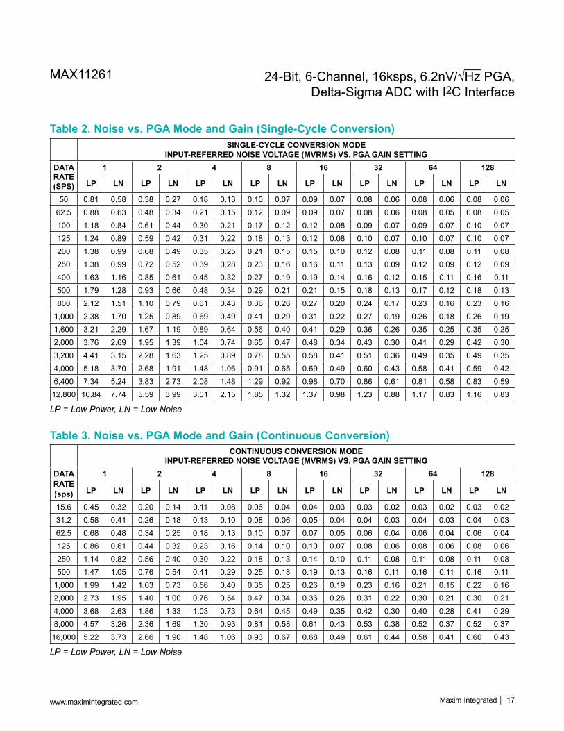
Table 2. Noise vs. PGA Mode and Gain (Single-Cycle Conversion)
Table 3. Noise vs. PGA Mode and Gain (Continuous Conversion)
SINGLE-CYCLE CONVERSION MODE INPUT-REFERRED NOISE VOLTAGE (ΜVRMS) VS. PGA GAIN SETTING
DATA RATE (SPS)
1 2 4 8 16 32 64 128
LP LN LP LN LP LN LP LN LP LN LP LN LP LN LP LN
50 0.81 0.58 0.38 0.27 0.18 0.13 0.10 0.07 0.09 0.07 0.08 0.06 0.08 0.06 0.08 0.0662.5 0.88 0.63 0.48 0.34 0.21 0.15 0.12 0.09 0.09 0.07 0.08 0.06 0.08 0.05 0.08 0.05100 1.18 0.84 0.61 0.44 0.30 0.21 0.17 0.12 0.12 0.08 0.09 0.07 0.09 0.07 0.10 0.07125 1.24 0.89 0.59 0.42 0.31 0.22 0.18 0.13 0.12 0.08 0.10 0.07 0.10 0.07 0.10 0.07200 1.38 0.99 0.68 0.49 0.35 0.25 0.21 0.15 0.15 0.10 0.12 0.08 0.11 0.08 0.11 0.08250 1.38 0.99 0.72 0.52 0.39 0.28 0.23 0.16 0.16 0.11 0.13 0.09 0.12 0.09 0.12 0.09400 1.63 1.16 0.85 0.61 0.45 0.32 0.27 0.19 0.19 0.14 0.16 0.12 0.15 0.11 0.16 0.11500 1.79 1.28 0.93 0.66 0.48 0.34 0.29 0.21 0.21 0.15 0.18 0.13 0.17 0.12 0.18 0.13800 2.12 1.51 1.10 0.79 0.61 0.43 0.36 0.26 0.27 0.20 0.24 0.17 0.23 0.16 0.23 0.16
1,000 2.38 1.70 1.25 0.89 0.69 0.49 0.41 0.29 0.31 0.22 0.27 0.19 0.26 0.18 0.26 0.191,600 3.21 2.29 1.67 1.19 0.89 0.64 0.56 0.40 0.41 0.29 0.36 0.26 0.35 0.25 0.35 0.252,000 3.76 2.69 1.95 1.39 1.04 0.74 0.65 0.47 0.48 0.34 0.43 0.30 0.41 0.29 0.42 0.303,200 4.41 3.15 2.28 1.63 1.25 0.89 0.78 0.55 0.58 0.41 0.51 0.36 0.49 0.35 0.49 0.354,000 5.18 3.70 2.68 1.91 1.48 1.06 0.91 0.65 0.69 0.49 0.60 0.43 0.58 0.41 0.59 0.426,400 7.34 5.24 3.83 2.73 2.08 1.48 1.29 0.92 0.98 0.70 0.86 0.61 0.81 0.58 0.83 0.59
12,800 10.84 7.74 5.59 3.99 3.01 2.15 1.85 1.32 1.37 0.98 1.23 0.88 1.17 0.83 1.16 0.83
LP = Low Power, LN = Low Noise
CONTINUOUS CONVERSION MODEINPUT-REFERRED NOISE VOLTAGE (ΜVRMS) VS. PGA GAIN SETTING
DATARATE(sps)
1 2 4 8 16 32 64 128
LP LN LP LN LP LN LP LN LP LN LP LN LP LN LP LN
15.6 0.45 0.32 0.20 0.14 0.11 0.08 0.06 0.04 0.04 0.03 0.03 0.02 0.03 0.02 0.03 0.0231.2 0.58 0.41 0.26 0.18 0.13 0.10 0.08 0.06 0.05 0.04 0.04 0.03 0.04 0.03 0.04 0.0362.5 0.68 0.48 0.34 0.25 0.18 0.13 0.10 0.07 0.07 0.05 0.06 0.04 0.06 0.04 0.06 0.04125 0.86 0.61 0.44 0.32 0.23 0.16 0.14 0.10 0.10 0.07 0.08 0.06 0.08 0.06 0.08 0.06250 1.14 0.82 0.56 0.40 0.30 0.22 0.18 0.13 0.14 0.10 0.11 0.08 0.11 0.08 0.11 0.08500 1.47 1.05 0.76 0.54 0.41 0.29 0.25 0.18 0.19 0.13 0.16 0.11 0.16 0.11 0.16 0.11
1,000 1.99 1.42 1.03 0.73 0.56 0.40 0.35 0.25 0.26 0.19 0.23 0.16 0.21 0.15 0.22 0.162,000 2.73 1.95 1.40 1.00 0.76 0.54 0.47 0.34 0.36 0.26 0.31 0.22 0.30 0.21 0.30 0.214,000 3.68 2.63 1.86 1.33 1.03 0.73 0.64 0.45 0.49 0.35 0.42 0.30 0.40 0.28 0.41 0.298,000 4.57 3.26 2.36 1.69 1.30 0.93 0.81 0.58 0.61 0.43 0.53 0.38 0.52 0.37 0.52 0.37
16,000 5.22 3.73 2.66 1.90 1.48 1.06 0.93 0.67 0.68 0.49 0.61 0.44 0.58 0.41 0.60 0.43
LP = Low Power, LN = Low Noise
www.maximintegrated.com Maxim Integrated │ 17
MAX11261 24-Bit, 6-Channel, 16ksps, 6.2nV/√Hz PGA, Delta-Sigma ADC with I2C Interface

I2C ProtocolThe I2C-compatible serial interface consists of the standard I2C signals: SCL and SDA. The SCL and the SDA pins are bidirectional lines, connected to a positive supply voltage via a current source or a pullup resistor. The data is clocked into the MAX11261 from the SDA pin on the rising edge of SCL. Data is clocked out of the MAX11261 on the SDA pin on the falling edge of SCL. The SCL/SDA have an open-drain pad for wired-AND connection on the bus. Fast Mode Plus protocol is supported at maximum SCL clock rate of 1MHz. Each device on the I2C bus is recognized by a unique device address and can operate as a transmitter and a receiver. The interface is backward compatible with Standard mode and Fast mode.Due to the variety of different devices (Bipolar, CMOS, NMOS) that can be connected to the I2C bus the input reference levels are set as 30% and 70% of VDVDD. The data on the SDA line must be stable during the high period of SCL. The HIGH or LOW state of SDA can only change when SCL is LOW for a normal byte transfer except for START and STOP conditions.All transactions begin with a START (S) and are terminated by a STOP (P). A high to low transaction on the SDA line while SCL is high defines a START condition. A low-to-high transition on the SDA line while SCL is high defines a STOP condition. The START and STOP are always generated by the I2C master. Every byte on the SDA line must be 8 bits long. The number of bytes that can be transmitted is unrestricted. Each byte must be followed by an acknowledge (ACK). Data is transferred with MSB first. The MAX11261 always sends out an ACK in response to the Master’s request for reading or writing data. If the MAX11261 receives a not acknowledge (NACK) from the master it will reset the I2C interface and wait for another START condition.
SCL (Serial Clock)The SCL pin synchronizes data communication between the host device and the MAX11261. Data is latched into the MAX11261 on the rising edge of SCL and data is shifted out of the MAX11261 on the falling edge of SCL. The MAX11261 does not support SCL clock stretching.
SDA (Serial Data Input/Output)The SDA line is considered an input when the master is transmitting the data to the MAX11261. The SDA line will be used as an output when the MAX11261 has data to be sent onto the I2C bus during a register read by the host master.The slave in the MAX11261 implements mandatory requirements as specified in the I2C standard, which are
detections of START and STOP conditions and support for ACK/NACK. This slave only supports 7-bit addressing and does not support general call address.
RDYB_INTB (Data Ready and Interrupt)In sequencer modes 1, 2, and 3, RDYB_INTB indicates the ADC conversion status and the availability of the conversion result. When RDYB_INTB is low, a conversion result is available. When RDYB_INTB is high, a conversion is in progress and the data for the current conversion is not available. RDYB_INTB is driven high after a complete FIFO read. RDYB_INTB resets to high four master clock cycles prior to the next FIFO register update.If data was read, then RDYB_INTB transitions from high to low at the output data rate. If the previous data was not read, the RDYB_INTB transitions from low to high for four master clock cycles and then transitions from high to low. In continuous mode, RDYB_INTB remains high for the first four conversion results and on the 5th result, RDYB_INTB goes low.For sequencer mode 2 and sequencer mode 3 the RDYB_INTB behavior for a multichannel conversion can be controlled by the SEQ:RDYBEN bit. The default value of SEQ:RDYBEN is ‘0’. When set to ‘0’, RDYB_INTB for a multichannel conversion behaves the same as a single channel operation. The RDYB_INTB toggles high to low after each channel is ready to update its corresponding data register. After the channel data is read, the RDYB_INTB will reset back to ‘1’. If the channel data is not read and the next channel is ready to update its data, the RDYB_INTB will toggle low to high four cycles before the data update (similar to a single channel case), and then toggle high to low indicating the new channel’s conversion data is available. If ‘N’ channels are enabled, RDYB_INTB will toggle high to low ‘N’ times. If SEQ:RDYBEN is set to ‘1’, the RDYB_INTB event for each channel is suppressed. The RDYB_INTB toggles high to low when the last channel is ready to update its corresponding data register and a single high-to-low transition happens.In sequencer modes 1, 2, and 3, RDYB_INTB is also ORing the FIFO usage interrupt outputs.RDYB_INTB is used as an interrupt in sequencer mode 4, so it has no significance in terms of indicating data availability when operating in sequencer mode 4.The STAT:SRDY[5:0] bits get set to ‘1’ when their corresponding channel finishes converting irrespective of the RDYBEN setting for sequencer modes 2, 3, and 4. The conversion status is available by reading STAT:MSTAT bit. This stays high as long as the modulator is converting.
www.maximintegrated.com Maxim Integrated │ 18
MAX11261 24-Bit, 6-Channel, 16ksps, 6.2nV/√Hz PGA, Delta-Sigma ADC with I2C Interface

I2C SequenceThe master needs to send out the first byte with a valid device address. The last bit of the first byte is a R/W bit and the master needs to send a '0' in this bit. The device will ignore a '1' sent in this bit. This is followed by a COMMAND BYTE for the MAX11261 as described in the command structure. The MAX11261 then responds to the command request depending on the MODE bit in the command.
Writing a Command to the MAX11261 for Conversion/ Calibration/Power-Down1) I2C START2) I2C WRITE
a. Send Device Address with a '0' in bit 8 indicating the master will send a command byte followed by the device address. (8’b011xxxx_0)
b. Check Acknowledgec. Send Command byte to convert/power down/
calibrate (8’b10_01_xxxx)d. Check acknowledge
3) I2C STOP
Sequence to Execute I2C Write Operation1) I2C START2) I2C WRITE
a. Send Device Address with a '0' in bit 8 indicating the master will send a command byte followed by the device address. (8’b011xxxx_0)
b. Check Acknowledgec. Send Command byte to Write registers
(8’b11_reg_addr[4:0]_0)d. Check acknowledgee. Send 8-bit register data MSB firstf. Check Acknowledgeg. …h. Check Acknowledge
3) I2C STOP
Sequence to Execute I2C Read Operation1) I2C START2) I2C WRITE
a. Send Device Address with a '0' in bit 8 indicating the master will send a command byte followed by the device address. (8’b011xxxx_0)
b. Check Acknowledgec. Send Command byte to Read registers
(8’b11_reg_addr[4:0]_1)d. Check Acknowledge
3) I2C Repeat START4) I2C WRITE
a. Send Device Address with a '1' in bit 8 indicating the master will read the register data out.
b. Check Acknowledge5) I2C READa. Receive 8 bits of Data
b. Send Acknowledgec. …d. Receive 8 bits of Datae. Send Not Acknowledge
6) I2C STOP
I2C Timing CharacteristicsThe I2C timing diagram is shown in Figure 1. The bus timing requirements are specified in I2C Timing Requirements table. The data is sampled on the positive edge of SCL and launched on negative edge of SCL for ACK and DATA reads. This gives a sufficient hold time for the master to sample the data.
Figure 4. RDYB
SCL/SDA
RDYBSCYCLE = '1',CONTSC = '1'
RDYB
N x tCNV
SCYCLE = '1',CONTSC = '0'
RDYB
tCNV5 tCNV
SCYCLE = '0',CONTSC = 'x'
DATA NOT RETRIEVE D
DATARETRIEVED
CONVERT COMMANDS
t CNV
N x t CNV
RATE[3:0] ≥ 13
RDYBSCYCLE = '0',CONTSC = 'x'
RATE[3:0] < 13
tCNV +tINIT
tINIT
NOTE: RATE[3:0] < 13, tINIT = 3µs.
www.maximintegrated.com Maxim Integrated │ 19
MAX11261 24-Bit, 6-Channel, 16ksps, 6.2nV/√Hz PGA, Delta-Sigma ADC with I2C Interface

I2C Device Addressing SchemeThe I2C slave has a 7-bit long device address. The device address is followed by a R/W bit which is low for a write command and high for a read command.The first three most significant bits of the device address are always 011. Slave address bits A[4:1] correspond by the matrix in Table 4 to the states of the device address bumps AD0 and AD1.The AD0 and AD1 bumps can be connected to any of the three signals: DGND, DVDD, and SDA giving 3 possible addresses for each bump allowing up to 9 devices connected to the bus (see Figure 5).
Modes and RegistersThe MAX11261 interface operates in two fundamental modes, either to issue a conversion command or to access registers. The mode of operation is selected by a command byte. Every I2C transaction to the MAX11261 starts with a command byte. The command byte begins with the MSB (B7) set to ‘1’. The next bit (B6) determines whether a conversion command is sent or register read/write access is requested.
Command ByteThe conversion command sets the mode of operation (conversion, calibration, or power-down) as well as the conversion speed of the MAX11261. The register read/write command specifies the register address as well as the direction of the access (read or write).
Table 4. I2C Device Address Mapping (Up to 9 Devices Selected on the I2C Bus Using the Following Addressing Scheme; I2C Addresses Are Not Contiguous)
ADDRESS PINS DEVICE ADDRESSADR1 ADR0 A7 A6 A5 A4 A3 A2 A1 A0DGND DGND
0 1 1
0 0 0 0 R/W
DGND DVDD 0 0 0 1 R/W
DGND SDA 0 0 1 1 R/W
DVDD DGND 0 1 0 0 R/W
DVDD DVDD 0 1 0 1 R/W
DVDD SDA 0 1 1 1 R/W
SDA DGND 1 1 0 0 R/W
SDA DVDD 1 1 0 1 R/W
SDA SDA 1 1 1 1 R/W
Table 5. Command Byte DefinitionB7(MSB) B6 B5 B4 B3 B2 B1 B0
Conversion Command 1 0 MODE1 MODE0 RATE3 RATE2 RATE1 RATE0
Register Read/Write 1 1 RS4 RS3 RS2 RS1 RS0 R/W
Figure 5. I2C
SDA
SCL
0 1 1 A4 A3 A2 A1 ACKR/W
www.maximintegrated.com Maxim Integrated │ 20
MAX11261 24-Bit, 6-Channel, 16ksps, 6.2nV/√Hz PGA, Delta-Sigma ADC with I2C Interface

Channel SequencingChanging SEQUENCER ModesMode Exit(See Table 9. Register Map for Register Definitions)To exit any of the four sequencer modes program the following sequence:1) Issue a power-down command to exit the conversion
process to STANDBY or SLEEP, as defined in CTRL1:PD[1:0]:a. Write a conversion command byte (see Table 5. Command Byte Definition) and set MODE[1:0] of the command byte to ‘01’2) Wait for STAT:PDSTAT[1:0] = ‘01’ (SLEEP) or STAT:PDSTAT[1:0] = ‘10’ (STANDBY).
Note: In all sequencer modes, the default exit state is SLEEP with the following exceptions where the exit state is defined by CTRL1:PD[1:0]:
● Sequencer mode 1 continuous conversion (CTRL1:SCYCLE = ‛0’)
● Sequencer mode 1 continuous single-cycle conversion (CTRL1:SCYCLE = ‛1’ and CTRL1:CONTSC = ‛1’)
Mode ChangeTo change sequencer modes or to update the SEQ register program the following sequence:1) Perform Sequencer Mode Exit (see the Mode Exit
section).2) Set up the following registers: SEQ, CTRL1.
a. Set SEQ:MODE[1:0] to select the new sequencer mode.
b. Set CTRL1:PD[1:0] to STANDBY or SLEEP state to set the desired exit state if a conversion command with MODE[1:0] set to ‘01’ is issued during the conversion.
3) Write the command byte (see Table 5)a. Set MODE[1:0] of command byte to “11”
(sequencer mode)4) Wait for STAT:PDSTAT[1:0] = “00” to confirm conversion
mode.
SEQUENCER MODE 1—Single-Channel Conversion with GPO Control and MUX DelaysThis mode is used for single-channel conversions where the sequencer is disabled. Figure 6 illustrates the timing. To support high-impedance source networks, the conversion delay (SEQ:MDREN) feature must be enabled. The states of the GPO bumps are configured using the GPO_DIR registers and can be modified anytime during mode 1 operation. The values of the CHMAP0/CHMAP1 registers and DELAY:GPO[7:0] bits are ignored in this mode.
BIT NAME DESCRIPTION
MODE[1:0]
The MODE bits are used to set the functional operation of the MAX11261 according to the following decoding.MODE1 MODE0 DESCRIPTION
0 0 Unused0 1 Power-down performed based on the CTRL1:PD[1:0] setting1 0 Calibration performed based on the CTRL1:CAL[1:0] setting1 1 Sequencer mode. The operation is based on the configuration of the SEQ register
RATE[3:0] These bits determine the conversion speed of the MAX11261. The decoding is shown in Table 1.RS[4:0] Register address as shown in Table 9.
R/W The R/W bit enables either a read or a write access to the address specified in RS[4:0]. If R/W is set to ‘0’, then data is written to the register. If the bit is set to ‘1’, then data is read from the register.
Table 6. Command Byte Decoding
Figure 6. Sequence Mode 1
SEQUENCER MODE 1
DEL CHANNEL CONVERSION
SEQ:MUX[2:0]
SEQ:MDREN· DELAY:MUX
www.maximintegrated.com Maxim Integrated │ 21
MAX11261 24-Bit, 6-Channel, 16ksps, 6.2nV/√Hz PGA, Delta-Sigma ADC with I2C Interface

Programming SequenceMode Entry1) Set up the following registers: SEQ, DELAY, CTRL1,
GPO_DIR.a. SEQ:MODE[1:0] = ‘00’ for sequencer mode 1.b. SEQ:MUX[2:0] to select the channel for
conversion.c. Enable SEQ:MDREN to delay conversion start to
allow for input settling. Set DELAY:MUX[7:0] to the desired conversion delay.
d. Set CTRL1:SCYCLE for either single cycle (no latency) or continuous conversion.
e. If single-cycle conversion is selected, set CTRL1:CONTSC to ‘1’ if continuous single-cycle conversion is desired
f. Set CTRL1:PD[1:0] to STANDBY or SLEEP state to set the desired exit state if a conversion command with MODE[1:0] set to ‘01’ is issued during the conversion.
g. Set register GPO_DIR to enable or disable the desired GPO bumps.
2) Write a conversion command (see Table 5, Command Byte Definition).a. Set data rate using bits RATE[3:0] of the
command byte.b. Set MODE[1:0] of the command byte to ‘11’ for
sequencer mode.3) Monitor RDYB_INTB for availability of conversion results
in the FIFO register (See Figure 4 for RDYB timing).
Mode Exit1) In single-cycle conversion mode (CTRL1:SCYCLE =
’1’) the sequencer exits into SLEEP state.
2) In continuous conversion mode (CTRL1: SCYCLE = ’0’ or (CTRL:SCYCLE = ’1’ and CTRL1:CONTSC = ’1’)), conversions continue nonstop until the mode is exited. To interrupt and exit continuous conversion or con-tinuous single-cycle conversion follow the Changing SEQUENCER Modes - Mode Exit section to put the part into STANDBY or SLEEP state based on CTRL1:PD[1:0] set in step 1(f) of Mode Entry section.
Changing Input Channel During Continuous Single-Cycle Conversion in Mode 11) Issue a conversion command with MODE[1:0] set
to ‘01’ to exit the conversion process to STANDBY or SLEEP state (see the Changing SEQUENCER Modes—Mode Exit section).
2) Monitor STAT:PDSTAT = ‘10’ or ‘01’ to confirm exit to STANDBY or SLEEP state.
3) Set SEQ:MUX[2:0] to select the new channel for conversion.
4) Write a conversion command (see Table 5) and set MODE[1:0] of command byte to ‘11’.
SEQUENCER MODE 2 – Multichannel Scan with GPO Control and MUX DelaysThis mode is used to sequentially convert a programmed set of channels in a preset order. Figure 7 illustrates the timing.The states of the GPO bumps are configured using the GPO_DIR register and can be modified anytime during mode 2 operation. In mode 2, register bits CHMAP0:CHn_ORD[2:0], CHMAP1:CHn_ORD[2:0], CHMAP0:CHn_EN, and CHMAP1:CHn_EN are used to select channels and conversion order. Bits DELAY:GPO[7:0], CHMAP0:CHn_GPO[2:0], CHMAP0:CHn_GPOEN, CHMAP1:CHn_GPO[2:0], and CHMAP1:CHn_GPOEN are ignored in this mode. The bit CTRL1:CONTSC is ignored and bit CTRL1:SCYCLE = ‘0’ is invalid in this mode.
Figure 7. Sequencer Mode 2 Timing Diagram
SEQUENCER MODE 2
SEQ:MDREN •DELAY:MUX
CHANMAP:ORD[2:0] = 001
DELCHANNEL
CONVERSIONDEL DEL DEL DEL DEL
CHANNEL CONVERSION
CHANNEL CONVERSION
CHANNEL CONVERSION
CHANNEL CONVERSION
CHANNEL CONVERSION
CHANMAP:ORD[2:0] = 010
SEQ:MDREN • DELAY:MUX
SEQ:MDREN • DELAY:MUX
CHANMAP:ORD[2:0] = 011
SEQ:MDREN • DELAY:MUX
CHANMAP:ORD[2:0] = 100
SEQ:MDREN • DELAY:MUX
CHANMAP:ORD[2:0] = 101
SEQ:MDREN • DELAY:MUX
CHANMAP:ORD[2:0] = 110
www.maximintegrated.com Maxim Integrated │ 22
MAX11261 24-Bit, 6-Channel, 16ksps, 6.2nV/√Hz PGA, Delta-Sigma ADC with I2C Interface

Programming SequenceMode Entry1) Set up the following registers: SEQ, CHMAP0,
CHMAP1, DELAY, GPO_DIR, CTRL1.a. SEQ:MODE[1:0] = ‘01’ for sequencer mode 2.b. If desired set SEQ:RDYBEN to ‘1’ to signal data
ready only when all channel conversions are completed.
c. Enable SEQ:MDREN to delay conversion start to allow for input settling. Set DELAY:MUX[7:0] to the desired conversion delay.
d. Set CHMAP0 and CHMAP1 to select the channels and channel order for conversion.
e. Set CTRL1:PD[1:0] to STANDBY or SLEEP state to set the desired exit state if a conversion command with MODE[1:0] set to ‘01’ is issued during the conversion.
f. Set register GPO_DIR to enable or disable the desired GPO bumps.
g. Set CTRL1:SCYCLE = ‘1’ for single-cycle conversion mode.
2) Write a conversion command (see Table 5).a. Set data rate using bits RATE[3:0] of the command
byte.
b. Set MODE[1:0] of the command byte to ‘11’.3) Monitor RDYB_INTB (if SEQ:RDYBEN = ’0’) and bits STAT:SRDY[5:0] for availability of per channel conversion results in FIFO registers.
Mode Exit1) This mode exits to SLEEP state upon completion of
sequencing all channels2) To interrupt current sequencing perform mode exit, see
the Changing SEQUENCER Modes—Mode Exit section. This device is put in STANDBY or SLEEP state based on CTRL1:PD[1:0] set in step 1(e) of Mode Entry section.
SEQUENCER MODE 3 – Scan, With Sequenced GPO ControlsThis mode is used to sequentially convert a programmed set of channels in a preset order and sequence the GPO bumps concurrently. The GPO bumps are used to bias external circuitry such as bridge sensors; the common reference (GPOGND) is typically ground. After all channel conversions have completed, the MAX11261 automatically powers down into SLEEP mode. Figure 8 illustrates the Sequencer Mode 3 timing diagram for a three-channel scan. Register GPO_DIR is ignored in this mode as the output controls are controlled by the sequencer.
Figure 8. Sequencer Mode 3 Timing Diagram for a Three-Channel Scan
SEQUENCER MODE 3 TIMING
DEL2 TCONVERT
DELAY:GPO
GPO/GPIO ACTIVATED
SCAN CHANNEL #1
DEL2
GPO/GPIO ACTIVATED
CONVERSION STARTS
CHANMAP:ORD[2:0] = 001
CHANMAP:ORD[2:0] = 010
DEL2
GPO/GPIO ACTIVATED
CONVERSION STARTS
CHANMAP:ORD[2:0] = 011
DEL1
TCONVERT
TCONVERT
(TCONVERT AND DEL1) END TRIGGERMUX SELECTS CHANNEL
(TCONVERT AND DEL1) END TRIGGERMUX SELECTS CHANNEL
MUX SELECTS CHANNEL
CONVERSION STARTS
CONVERSION ENDS
SEQ:MDREN • DELAY:MUX
SCAN CHANNEL #2
SCAN CHANNEL #3
CONVERSION ENDS
CONVERSION ENDS
DEL1 – PROGRAMMED DELAY USING BITS DELAY:GPO[7:0] TO PROVIDE SUFFICIENT SETTLING TIME FOR THE SENSOR BEFORE THE FIRST CHANNEL IS CONVERTED.
DEL2 – PROGRAMMED DELAY USING BITS DELAY:MUX[7:0] FOR SENSOR AND ANALOG INPUT SETTLING AFTER THE MULTIPLIER SELECTS THE CHANNEL FOR CONVERSION.
www.maximintegrated.com Maxim Integrated │ 23
MAX11261 24-Bit, 6-Channel, 16ksps, 6.2nV/√Hz PGA, Delta-Sigma ADC with I2C Interface

Programming SequenceMode Entry1) Set up the following registers: SEQ, CHMAP0,
CHMAP1, DELAY, CTRL1, CTRL3.a. SEQ:MODE[1:0] = ”10” for sequencer mode 3.b. If desired set SEQ:RDYBEN to ‘1’ to signal data
ready only when all channel conversions are completed.
c. Enable SEQ:MDREN if conversion start is to be delayed to allow for input settling. Set DELAY:MUX[7:0] to the desired conversion delay.
d. Set CHMAP0 and CHMAP1 to enable the channels for conversion and the channel conversion order. Map the corresponding GPO bumps to a channel.
e. Enable SEQ:OCDREN for adding a delay before the multiplexer selects this channel for conversion. Set DELAY:GPO to a delay value sufficient for the bias to settle.
f. Set CTRL1:PD[1:0] to STANDBY or SLEEP state (desired exit state if an IMPD command is issued during the conversion).
g. Set CTRL1:SCYCLE = ‘1’ for single conversion mode.2) Write the command byte (see Table 5).
a. Set data rate using bits RATE[3:0] of command byte.
b. Set MODE[1:0] of command byte to “11”.3) Monitor RDYB_INTB (if SEQ:RDYBEN = ‘0’) and bits
STAT:SRDY[5:0] for availability of per channel conversion results in FIFO registers.
Mode Exit1) This mode exits to SLEEP state upon completion of sequencing all channels and output controls.
2) To interrupt current sequencing, perform mode exit. See the Changing SEQUENCER Modes - Mode Exit section, puts the part in STANDBY or SLEEP state based on CTRL1:PD[1:0] set in step 1(f) of Mode Entry.The bit CTRL1:CONTSC is ignored and bit CTRL1:SCYCLE = ‘0’ is invalid in this mode.
SEQUENCER MODE 4 – Autoscan with GPO Controls (CHMAP) and InterruptThis mode features a programmable timer to wake the MAX11261 from SLEEP and power down the MAX11261 between operations.The MAX11261 automatically cycles through a sequence of delay, power-up, operate the GPO, scan selected channels, perform math operations, and power-down into SLEEP state. See Figure 9.The duty cycle is programmed by DELAY:AUTOSCAN[7:0]. The programmed value must be greater than “0x00”, oth erwise power-down is skipped and followed immediately by another scan cycle. This sequence continues until the conversion is halted. The auto-scan delay is from 4ms to 1024ms.To generate SYNC signals for other slave devices, the master must configure AUTOSCAN[7:0] greater than “0x00”, otherwise the SYNC signal cannot be generated.In this mode, a register INT_STAT read will clear RDYB_INTB if the FIFO usage interrupts are not triggered. If any of the FIFO usage interrupts is triggered, RDYB_INTB will keep asserted. The user can disable the FIFO usage interrupts to allow only the input comparison to generate interrupts.The behavior of the RDYB_INTB pin ignores the SEQ:RDYBEN bit.
Figure 9. Sequencer Mode 4 Timing Diagram
SEQUENCER MODE 3
MATHAUTOSCAN
DELAY
FULL POWER-DOW N
DELAY:AUTOSCAN
SEQUENCER MODE 3
MATHAUTOSCAN
DELAYSEQUENCER
MODE 3MATH
POWER-UP
FULL POWER-DOW N
POWER-UP
FULLPOWER-DOW N
DELAY:AUTOSCAN
SEQUENCER MODE 4
www.maximintegrated.com Maxim Integrated │ 24
MAX11261 24-Bit, 6-Channel, 16ksps, 6.2nV/√Hz PGA, Delta-Sigma ADC with I2C Interface

The GPOs are operated by the sequencer and programmed by CHMAPx registers. GPO_DIR register is ignored in this mode. A DELAY:GPO[7:0] value of ‘0x00’ represents no delay. This mode also utilizes the channel MUX delay if enabled by setting the SEQ:MDREN bit to ‘1’. The value programmed into the DELAY:MUX[7:0] register will be used to delay the start of the conversion after selecting the channel. If the CTRL1:CONTSC bit is ‘1’, it is ignored in this mode. CTRL1:SCYCLE bit of ‘0’ is invalid in this mode.
Math Operation: the Conversion Result Processing and Out-Of-Range (OOR) Bit GenerationThere are 3 options to process the conversion results to detect if a channel input signal is changing. They are controlled by HPF:CMP_MODE[1:0] register. The conversion result processing is shown in Figure 10.In the following section, n indicates the channel number, N indicates a specific sample, N-1 indicates the previous sample of the same channel.1) CMP_MODE[1:0] = 0b00. Compare the current result
DATAn(N) with the user-programmable low limit (LIMIT_LOWn) and the high limit (LIMIT_HIGHn). If the conversion result is within LIMIT_LOWn and LIMIT_HIGHn, there is no OOR generated. Otherwise, an OOR is generated.
2) CMP_MODE[1:0] = 0b01. Subtract the current result DATAn(N) by the previous result DATAn(N-1). Then compare the resultant with the user-programmable low limit (LIMIT_LOWn) and the high limit (LIMIT_HIGHn). If the resultant is within LIMIT_LOWn and LIMIT_HIGHn, there is no OOR generated. Otherwise an OOR is generated. After writing HPF register with HPF:CMP_MODE[1:0] = 0b01, the comparator is initialized and the first conversion does not detect the OOR condition.
3) CMP_MODE[1:0] = 0b10. This option enables the high-pass digital filter, generating a high-pass filter output based on the user-programmable cut-off frequency register HPF:FREQUENCY[2:0]. Compare the HPF output with the user-programmable low limit (LIMIT_LOWn) and the high limit (LIMIT_HIGHn). If the HPF output is within LIMIT_LOWn and LIM-IT_HIGHn, there is no OOR generated. Otherwise an OOR is generated. Writing HPF register with HPF:CMP_MODE[1:0] = 0b10 resets the high-pass filter. The high-pass filter cut-off frequency is calculated as shown in Table 7.
4) CMP_MODE[1:0] = 0b11 is reserved.
Figure 10. Conversion Result Math Operation
Z-1 K
DATAn(N)
HIGH-PASS DIGITAL FILTER TO REMOVE BASELINE DRIFT
CMP_MODE[1:0]
DATAn(N-1)COMP
LIMIT_HIGHn
LIMIT_LOWn
OOR
0
1
2
3
MAX11261 CONVERSION RESULT PROCESSING
CHANNEL n CONVERSION
RESULT
www.maximintegrated.com Maxim Integrated │ 25
MAX11261 24-Bit, 6-Channel, 16ksps, 6.2nV/√Hz PGA, Delta-Sigma ADC with I2C Interface

Unipolar Mode Not SupportedThe math operations performed in this mode prevent using unipolar ranges. Only bipolar ranges and two’s complement numbers are used. The LIMIT_LOWn, LIMIT_HIGHn registers are bipolar two’s complement values.
Programming SequenceMode Entry1) Set up the following registers: SEQ, CHMAP0,
CHMAP1, DELAY.a. SEQ:MODE[1:0] = ”11” for sequencer mode 4.b. Enable SEQ:MDREN if conversion start is to
be delayed to allow for input settling. Write to DELAY:MUX[7:0] to set conversion delay.
c. Set HPF:MODE[1:0], LIMIT_LOWn, and LIMIT_HIGHn registers to desired values .
d. Set CHMAP0 and CHMAP1 to enable the channels for conversion and the channel conversion order. Map the GPO bump to a channel and enable it for the conversion process.
e. Enable SEQ:GPODREN for adding a delay (DEL1) before the multiplexer selects the first channel for conversion. See Figure 8 for timing. Set DELAY:GPO to a delay value sufficient for the bias to settle.
f. Set CTRL1:PD[1:0] to STANDBY or SLEEP state (desired exit state if an IMPD command is issued during the conversion).
g. Set CTRL1:SCYCLE = ‘1’ for single-conversion mode.
2) Write the command byte (see Table 5).a. Set data rate using bits RATE[3:0] of command
byte.b. Set MODE[1:0] of command byte to “11”.
3) This mode is perpetual, monitor interrupt signal RDYB_INTB for different interrupt requests.a. Per channel conversion data ready are available by reading bits STAT:SRDY[5:0] for analog input channel 5 to channel 0.b. Do not overwrite SEQ:MODE[1:0] during mode 4 operation. Write new SEQ:MODE[1:0] during mode exit, refer to Mode Exit 1a and 1b.
Mode Exit1) To exit to another sequencer mode.
a. Write SEQ:MODE[1:0] to the desired sequencer mode.
b. Issue conversion command.2) To exit to STANDBY or SLEEP state.
a. Follow the Changing SEQUENCER Modes—Mode Exit section to STANDBY or SLEEP state based on CTRL1:PD[1:0] set in Mode Entry step 1(f) above.
AUTOSCAN DELAYProgram delay using bits DELAY:AUTOSCAN[7:0] for selecting the scan rate. This is a power-saving feature for throttling system power consumption. During the autoscan delay period, the MAX11261 is powered down and woken up automatically.
Supplies and Power-On SequenceThe MAX11261 requires two power supplies, AVDD and DVDD. These power supplies can be sequenced in any order. The analog supply (AVDD) powers the analog inputs and the modulator. The DVDD supply powers the I2C interface. The low-voltage core logic can either be powered by the integrated LDO (default) or via DVDD. Figure 11 shows the two possible schemes. CAPREG denotes the internally generated supply voltage. If the LDO is used, the DVDD operating voltage range is from 2.0V to 3.6V. If the core logic is directly powered by DVDD (DVDD and CAPREG connected together), the DVDD operating voltage range is from 1.7V to 2.0V.
Table 7. HPF Cut-off Frequency vs HPF:FREQUENCY[2:0] Register Values
HPF:FREQUENCY[2:0] CUT-OFF FREQUENCY (HZ)
0 Scan Rate/39.06251 Scan Rate/78.1252 Scan Rate/156.253 Scan Rate/312.54 Scan Rate/6255 Scan Rate/12506 Scan Rate/25007 Scan Rate/5000
www.maximintegrated.com Maxim Integrated │ 26
MAX11261 24-Bit, 6-Channel, 16ksps, 6.2nV/√Hz PGA, Delta-Sigma ADC with I2C Interface
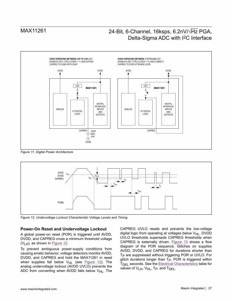
Power-On Reset and Undervoltage LockoutA global power-on reset (POR) is triggered until AVDD, DVDD, and CAPREG cross a minimum threshold voltage (VLH), as shown in Figure 12.To prevent ambiguous power-supply conditions from causing erratic behavior, voltage detectors monitor AVDD, DVDD, and CAPREG and hold the MAX11261 in reset when supplies fall below VHL (see Figure 12). The analog undervoltage lockout (AVDD UVLO) prevents the ADC from converting when AVDD falls below VHL. The
CAPREG UVLO resets and prevents the low-voltage digital logic from operating at voltages below VHL. DVDD UVLO thresholds supersede CAPREG thresholds when CAPREG is externally driven. Figure 13 shows a flow diagram of the POR sequence. Glitches on supplies AVDD, DVDD, and CAPREG for durations shorter than TP are suppressed without triggering POR or UVLO. For glitch durations longer than TP, POR is triggered within TDEL seconds. See the Electrical Characteristics table for values of VLH, VHL, TP, and TDEL.
Figure 11. Digital Power Architecture
Figure 12. Undervoltage Lockout Characteristic Voltage Levels and Timing
ANALOG 2V DIGITAL
LOGIC
DIGITALINTERFACE
INPUTS AND
OUTPUTS
LDO
CAPREG 220nF0603X7R
DGND
AVDD DVDD
MAX11261
ANALOG 2V DIGITAL
LOGIC
DIGITALINTERFACE
INPUTS AND
OUTPUTS
LDO
CAPREG
AVDD DVDD
MAX11261
DVDD OPERATING BETWEEN 2.0V TO 3.6V LDO ENABLED (SET CTRL2:LDOEN = ‘1’) AND BYPASS CAPREG TO DGND WITH 220nF
DVDD OPERATING BETWEEN 1.7V TO 2.0V LDO DISABLED (SET CTRL2:LDOEN = ‘0’) AND CONNECT CAPREG TO DVDD AT BOARD LEVEL
AVDDDVDD
CAPREG
PORB
TDEL
VHYSVHL
VLH
TP
TDEL
TP
www.maximintegrated.com Maxim Integrated │ 27
MAX11261 24-Bit, 6-Channel, 16ksps, 6.2nV/√Hz PGA, Delta-Sigma ADC with I2C Interface

Power-On-Reset TimingPower-on reset is triggered during power-up and under-voltage conditions as described above. Completion of the POR process is monitored by polling STAT:PDSTAT[1:0] = ‘10’ for STANDBY state (see Figure 14).
ResetHardware Reset Using RSTBThe MAX11261 features an active-low RSTB bump to perform a hardware reset. Pulling the RSTB bump low stops any conversion in progress, reconfigures the internal registers to the power-on reset state and resets all digital filter states to zero. After the reset cycle is completed, the
MAX11261 remains in STANDBY state and awaits further commands.
Software ResetThe host can issue a software reset to restore the default state of the MAX11261. A software reset sets the interface registers back into their default states and resets the inter-nal state machines. However, a software reset does not emulate the complete POR or hardware reset sequence.Two I2C transactions are required to issue a software reset: First set CTRL1:PD[1:0] to ‘11’ (RESET). Then issue a conversion command with MODE[1:0] set to ‘01’. To confirm the completion of the reset operation, STAT:PDSTAT and STAT:INRESET must be monitored.
Figure 13. MAX11261 UVLO and POR Flow Diagram
Figure 14. Power-On Reset and PDSTAT Timing
CAPREG UVLOTRIGGERED?
POWER-ON RESET FOR 2V DIGITAL LOGIC
YES
ANALOG RESET
NOAVDD UVLO TRIGGERED?
YES
NO
OSCILLATOR RESET
DVDD UVLO TRIGGERED?
POWER-ON RESET FOR DIGITAL LOGIC
AND INTERFACE
YES
NO
POWER-ON
VDVDD
‘11’STAT:PDSTAT=’XX’ ‘10’ (STANDBY)
IN POWER-ON RESET
OUT OF POWER-ON RESETSERIAL INTERFACE READ ONLY
SERIAL INTERFACE AVAILABLE FOR BOTH READ AND WRITE
www.maximintegrated.com Maxim Integrated │ 28
MAX11261 24-Bit, 6-Channel, 16ksps, 6.2nV/√Hz PGA, Delta-Sigma ADC with I2C Interface

Table 8. Maximum Delay Time for Mode TransitionsCOMMAND
ISSUEDCHIP STATE
BEFORE COMMAND COMMAND INTERPRETATION MAXIMUM DELAY TIME TO NEXT STATE†
CHIP STATE AFTER COMMAND
SLEEP
RESET Command ignored 0 RESETSLEEP Command ignored 0 SLEEP
STANDBY Chip powers down into a leakage-only state 20ms SLEEP
STANDBY (fast)***Issue a conversion command and then monitor STAT:PDSTAT[1:0] for change of mode then send IMPD command
15μs SLEEP
Calibration Calibration stops, chip powers down into a leakage-only state 3μs SLEEP
Conversion Conversion stops, chip powers down into a leakage-only state 3μs SLEEP
Mode 4 convert** LDO wake-up and overhead TPUPSLP* + 3μs SLEEP
CONVERTSLEEP
Mode change from SLEEP to conversionFrom conversion command to PD-STAT=”00”
TPUPSLP* + 3μs CONVERT
STANDBY STANDBY to conversion TPUPSBY* + 3μs CONVERT
STANDBY
RESET Command ignored 0 RESETSLEEP SLEEP to STANDBY 20ms STANDBY
SLEEP (fast)***
Mode change from SLEEP to STANDBY via conversion operation. The delay includes SLEEP state power-up time (TPUPSLP*) and switching time from slow standby clock to high-speed MCLK.
85μs STANDBY
STANDBY Command ignored 0 STANDBYCalibration Calibration stops 3μs STANDBYConversion Conversion stops 3μs STANDBY
Mode 4 SLEEP** LDO wake-up and overhead TPUPSLP* + 3μs STANDBY
RESET
RESET Command ignored 0 RESETSLEEP Command ignored 0 SLEEP
STANDBY Register values reset to default 28ms STANDBY
Calibration Calibration stops, register values reset to default 6μs STANDBY
Conversion Conversion stops, register values reset to default 6μs STANDBY
POR OFF From complete power-down to STANDBY state 10ms STANDBY
RSTB Any From any state to STANDBY mode 10ms STANDBY
†Guaranteed by design *See Electrical Characteristics table. **During wake-up transition switching between SLEEP and CONVERT states. ***Assume full active power during these state transitions.
www.maximintegrated.com Maxim Integrated │ 29
MAX11261 24-Bit, 6-Channel, 16ksps, 6.2nV/√Hz PGA, Delta-Sigma ADC with I2C Interface

Figure 15 shows the state transition for the RESET command and the relative timing of STAT register update. During reset, INRESET = ’1’ and PDSTAT= ‘11’. The I2C interface cannot be written until MAX11261 enters STANDBY state where PDSTAT = ‘10’. To confirm completion of the RESET command, monitor for INRESET = ‘0’ and PDSTAT = ‘10’. Table 8 summarizes the maximum delay for reset operation.The commands are defined as follows:
SLEEP: Set CTRL1:PD[1:0] to ‘01’; issue a conversion command with MODE[1:0] set to ‘01’STANDBY: Set CTRL1:PD[1:0] to ‘10’; issue a conversion command with MODE[1:0] set to ‘01’RESET: Set CTRL1:PD[1:0] to ‘11’; issue a conversion command with MODE[1:0] set to ‘01’CONVERT: Any conversion command with MODE[1:0] set to ‘11’POR: Power-on reset during initial power-up or UVLORSTB: Hardware reset with RSTB bump
Power-Down StatesTo reduce overall power consumption, the MAX11261 features two power-down states: STANDBY and SLEEP. In SLEEP mode all circuitry is powered down, and the supply currents are reduced to leakage currents. In STANDBY mode the internal LDO and a low-frequency oscillator are powered up to enable fast start-up. After POR or a hardware reset the MAX11261 is in STANDBY mode until a command is issued.
Changing Power-Down StatesMode transition times are dependent on the current mode of operation. STAT:PDSTAT is updated at the end of all
mode changes and is a confirmation of a completed trans-action. The MAX11261 does not use a command FIFO or queue. The user must confirm the completed transaction by polling STAT:PDSTAT after the expected delay, as described in Table 8. Once the transition is complete, it is safe to send the next command.Verify that STAT:PDSTAT indicates the desired state before issuing a conversion command.Writes to any CTRL register during a conversion aborts the conversion and returns the MAX11261 to STANDBY state.
SLEEP STATE TO STANDBY STATE (FAST)1) Set CTRL1:PD[1:0] = ‘10’ for STANDBY state.2) Set SEQ:MODE[1:0] = ‘00’ for sequencer mode 1.3) Issue a conversion command with MODE[1:0] set to
‘11’.4) Monitor STAT:PDSTAT[1:0] = ‘00’ for active state.5) Write the conversion command with MODE[1:0] set to
‘01’.6) Monitor STAT:PDSTAT = ‘10’ for completion.
STANDBY STATE TO SLEEP STATE (FAST)1) Set CTRL1:PD[1:0] = ‘01’ for STANDBY state.2) Set SEQ:MODE[1:0] = ‘00’ for sequencer mode 1.3) Issue a conversion command with MODE[1:0] set to
‘11’.4) Monitor STAT:PDSTAT[1:0] = ‘00’ for active state.5) Write the conversion command with MODE[1:0] set to
‘01’.6) Monitor STAT:PDSTAT = ‘01’ for completion.
Figure 15. STAT:INRESET and STAT:PDSTAT Timing
RESET COMMAND
STAT:INRESET
‘11’STAT:PDSTAT = ‘00’/’10' ‘10’
IDLE
SERIAL INTERFACE IS READONLY DURING THIS PERIOD
SERIAL INTERFACE IS AVAIABLE FOR BOTH
READ AND WRITECOMMAND LATCHED
www.maximintegrated.com Maxim Integrated │ 30
MAX11261 24-Bit, 6-Channel, 16ksps, 6.2nV/√Hz PGA, Delta-Sigma ADC with I2C Interface
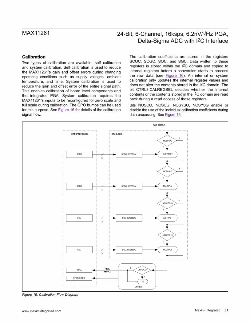
CalibrationTwo types of calibration are available: self calibration and system calibration. Self calibration is used to reduce the MAX11261’s gain and offset errors during changing operating conditions such as supply voltages, ambient temperature, and time. System calibration is used to reduce the gain and offset error of the entire signal path. This enables calibration of board level components and the integrated PGA. System calibration requires the MAX11261’s inputs to be reconfigured for zero scale and full scale during calibration. The GPO bumps can be used for this purpose. See Figure 16 for details of the calibration signal flow.
The calibration coefficients are stored in the registers SCOC, SCGC, SOC, and SGC. Data written to these registers is stored within the I2C domain and copied to internal registers before a conversion starts to process the raw data (see Figure 16). An internal or system calibration only updates the internal register values and does not alter the contents stored in the I2C domain. The bit CTRL3:CALREGSEL decides whether the internal contents or the contents stored in the I2C domain are read back during a read access of these registers.Bits NOSCO, NOSCG, NOSYSO, NOSYSG enable or disable the use of the individual calibration coefficients during data processing. See Figure 16.
Figure 16. Calibration Flow Diagram
SUBTRACTSCOC
MULTIPLYSCGC
SUBTRACTSOC
MULTIPLYSGC
DATA
NOSCO=0
NOSCG=0
T
F
T
F
NOSYSO=0
T
F
NOSYSG=0F
T
STATUS REG
CAL BLOCKINTERFACE BLOCK
UNIPOLAR
x2
F
T
LIMITER
SCOC_INTERNAL
SCGC_INTERNAL
SOC_INTERNAL
SGC_INTERNAL
24
24
24
24
RAW RESULT
FINALRESULT
www.maximintegrated.com Maxim Integrated │ 31
MAX11261 24-Bit, 6-Channel, 16ksps, 6.2nV/√Hz PGA, Delta-Sigma ADC with I2C Interface

Self-CalibrationThe self-calibration is an internal operation and does not disturb the analog inputs. The self-calibration command can only be issued with the sequencer in mode 1 (SEQ:MODE[1:0] = “00”). Self-calibration is accom-plished in two independent phases, offset, and gain. The first phase disconnects the inputs to the modulator and shorts them together internally to develop a zero-scale signal. A conversion is then completed and the results are post-processed to generate an offset coefficient which cancels all internally generated offsets. The second phase connects the inputs to the reference to develop a full-scale signal. A conversion is then completed and the results are post-processed to generate a full-scale coeffi-cient, which scales the converters full-scale analog range to the full-scale digital range.The entire self-calibration sequence requires two independent conversions, one for offset and one for full scale. The conversion rate is 50sps in the single-cycle mode. This rate provides the lowest noise and most accurate calibrations.The self-calibration operation excludes the PGA. A system-level calibration is available in order to calibrate the PGA signal path.
System-CalibrationThis mode is used when calibration of board level components and the integrated PGA is required. The system calibration command is only available in sequencer mode 1. A system calibration requires the input to be configured to the proper level for calibration. The off-set and full-scale system calibrations are, therefore, performed using separate commands. The channel selected in the SEQ:MUX bits is used for system calibrations.To perform a system offset calibration, the inputs must be configured for zero scale. The inputs do not necessarily need to be shorted to 0V as any voltage within the range of the calibration registers can be nulled in this calibration.A system offset calibration is started as follows: Set CTRL1:CAL[1:0] to ‘01’ (system offset calibration). Then issue a conversion command with the MODE[1:0] bits set to ‘10’ (calibration). The system offset calibration requires 100ms to complete.To perform a system full-scale calibration, the inputs must be configured for full scale. The input full-scale value does not necessarily need to be equal to VREF since the input voltage range of the calibration registers can scale up or down appropriately within the range of the calibration registers.
A system full-scale calibration is started as follows: Set CTRL1:CAL[1:0] to ‘10’ (system full-scale calibration). Then issue a conversion command with the MODE[1:0] bits set to ‘10’ (calibration). The system full-scale calibration requires 100ms to complete. The GPO bumps can be used during a system calibration.All four calibration registers (SOC, SGC, SCOC, and SCGC) can be written by the host to store special calibration values. The new values will be copied to the internal registers at the beginning of a new conversion.
Components of the ADCModulatorMODULATOR DIGITAL OVERRANGEThe output of the SINC filter is monitored for overflow. When SINC filter overflow is detected, the STAT:DOR bit is set to ‘1’ and a default value is loaded into the FIFO register depending on the polarity of the overload. A positive overrange causes 0x7FFFFF to be written to the FIFO register. A negative overrange causes 0x800000 to be written to the FIFO register. See Table 9.
MODULATOR ANALOG OVERRANGEThe modulator analog overrange is used to signal the user that the input analog voltage has exceeded preset limits defined by the modulator operating range. These limits are approximately 120% of the applied reference voltage. When analog overrange is detected the STAT:AOR bit is set to ‘1’ after FIFO is updated. The AOR bit will always correspond to the current value in the FIFO register. See Table 9.The DATA values shown are for bipolar ranges with two’s complement number format. VOVRRNG is the overrange voltage value typically > 120% of VREF.
Table 9. Analog Overrange Behavior for Different Operating Conditions and Modes
STAT REGISTERINPUT VOLTAGE AOR DOR DATA
-VREF < VIN < VREF 0 0 RESULTVREF < VIN < VOVRRNG 1 0 RESULT-VOVRRNG < VIN < -VREF 1 0 RESULTVIN > VOVRRNG 1 1 0x7FFFFFVIN < -VOVRRNG 1 1 0x800000
www.maximintegrated.com Maxim Integrated │ 32
MAX11261 24-Bit, 6-Channel, 16ksps, 6.2nV/√Hz PGA, Delta-Sigma ADC with I2C Interface

SINC FilterThe digital filter is a mode-configurable digital filter and decimator that processes the data stream from the fourth order delta-sigma modulator and implements a fifth order SINC function with an averaging function to produce a 24-bit wide data stream.
The SINC filter allows the MAX11261 to achieve very high SNR. The bandwidth of the fifth order SINC filter is approx-imately twenty percent of the data rate. See Figure 17 and Figure 18 for the filter response of 16ksps and 4ksps, respectively. See Figure 19 for the bandwidth of the indi-vidual signal stages.
Figure 17. Digital Filter Frequency Response for 12.8ksps Single-Cycle Data Rate
Figure 18. Digital Filter Frequency Response for 4ksps Single-Cycle Data Rate
Figure 19. Signal Path Block Diagram Including Bandwidth of Each Stage
SINC5 FILTER, NORMAL MODE REJECTION DATA RATE 12800.0sps
FREQUENCY (Hz)
GAI
N (d
B)
x 104
2
-20-10
0
0 4
-40
-60
-80
-100
-120
-140
-160
-180
-200
-30
-50
-70
-90
-110
-130
-150
-170
-190
6 8 10 12
SINC5 FILTER, NORMAL MODE REJECTIONSINGLE CYCLE DATA RATE 4000.0sps
FREQUENCY (Hz)
GAI
N (d
B)
x 104
1
-20-10
0
0 2
-40
-60
-80
-100
-120
-140
-160
-180
-200
-30
-50
-70
-90
-110
-130
-150
-170
-190
3 4 5 6
DELTA-SIGMAADC
PGADIGITAL FILTER
N 24
G=128
Sn = 5nV/√Hz ANALOG FILTER
N
BW3 NEB10nF 23k 36k1nF 230k 361k100pF 2.3M 3.6M
BW3 NEB10nF 21k 33k1nF 69k 108k100pF 73k 115k
NEB2 = π /2 x BW3NEB1 = π /2 x BW3
NEB3 = 0.215 x FDATA
BW3 BW3 FDATANEB3
BW3
www.maximintegrated.com Maxim Integrated │ 33
MAX11261 24-Bit, 6-Channel, 16ksps, 6.2nV/√Hz PGA, Delta-Sigma ADC with I2C Interface

FIFO OperationThe MAX11261 stores conversion results in a 64-entry FIFO, which includes a holding register and 63 circular buffers.Each FIFO entry consists of 32 bits of data. From the MSB, they are the OVW bit (indicating the previous entry is overwritten), 3 bits reserved, the channel ID CH[2:0], the OOR bit (indicating the channel’s input is out-of-range by using the math operation), and the conversion result D[23:0].The register FIFO_LEVEL stores the number of conver-sion results currently held in the FIFO. In Figure 20, FIFO_LEVEL = 4.The first conversion result is stored in the holding regis-ter. And the next conversion results are stored in the 63 buffers sequentially. If there are more than 64 conversion results (e.g., 65) the first conversion result is kept in the holding register, the second conversion result is overwritten (lost), the 3rd conversion result is stored in BUF[1], and the OVW bit is set in BUF[1], indicating that the previous conversion result is overwritten. The 4th conversion result
is stored in BUF[2], and so on. The 65th conversion result is stored in BUF[0]. Only the results in the circular buffers will be overwritten.The FIFO read always starts from the oldest conversion result, which is held in the holding register. After all conversion results are read, the FIFO_LEVEL register is cleared to 0. When the FIFO is empty, a FIFO read returns 0xFFFF_FFFF.When reading the FIFO while the ADC is running it is important to first read the FIFO_LEVEL and then read the FIFO by the number of entries indicated by the FIFO_LEVEL. Reading more entries than are available in the FIFO (underflow) when the ADC is running can (albeit unlikely) result in data loss.To the user, the FIFO is a single addressable register. After one conversion result is transferred from the holding register to the user, the MAX11261 automatically moves the next conversion result to the holding register. The user can burst read the FIFO to reduce power consumption.
Figure 20. MAX11261 FIFO Structure
BUF(62)
BUF(61)
BUF(60)
BUF(3)
BUF(59)
BUF(0)
BUF(1)
BUF(2)
HOLDINGREGISTER
HOST
OVW CH[2:0]- - - OOR D[23:0]
MSB LSB
MAX11261 FIFO STRUCTURE
www.maximintegrated.com Maxim Integrated │ 34
MAX11261 24-Bit, 6-Channel, 16ksps, 6.2nV/√Hz PGA, Delta-Sigma ADC with I2C Interface
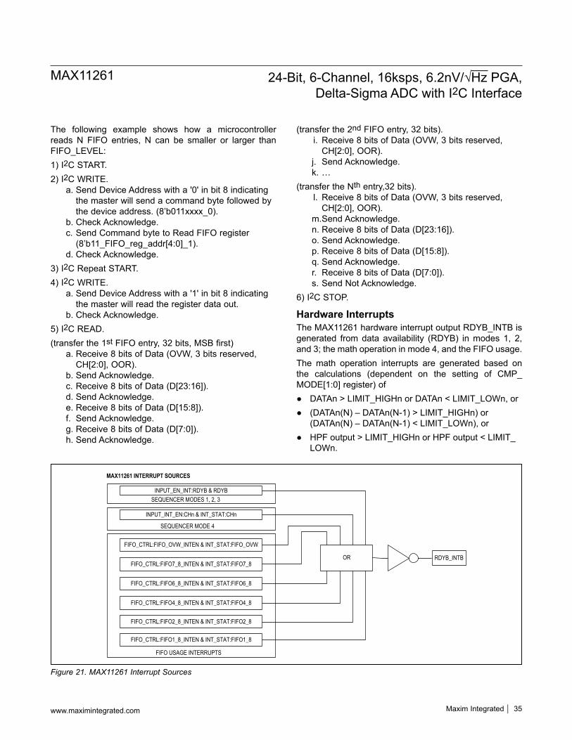
The following example shows how a microcontroller reads N FIFO entries, N can be smaller or larger than FIFO_LEVEL:1) I2C START.2) I2C WRITE.
a. Send Device Address with a '0' in bit 8 indicating the master will send a command byte followed by the device address. (8’b011xxxx_0).
b. Check Acknowledge.c. Send Command byte to Read FIFO register
(8’b11_FIFO_reg_addr[4:0]_1).d. Check Acknowledge.
3) I2C Repeat START.4) I2C WRITE.
a. Send Device Address with a '1' in bit 8 indicating the master will read the register data out.
b. Check Acknowledge.5) I2C READ.(transfer the 1st FIFO entry, 32 bits, MSB first)
a. Receive 8 bits of Data (OVW, 3 bits reserved, CH[2:0], OOR).
b. Send Acknowledge.c. Receive 8 bits of Data (D[23:16]).d. Send Acknowledge.e. Receive 8 bits of Data (D[15:8]).f. Send Acknowledge.g. Receive 8 bits of Data (D[7:0]).h. Send Acknowledge.
(transfer the 2nd FIFO entry, 32 bits).i. Receive 8 bits of Data (OVW, 3 bits reserved,
CH[2:0], OOR).j. Send Acknowledge.k. …
(transfer the Nth entry,32 bits).l. Receive 8 bits of Data (OVW, 3 bits reserved,
CH[2:0], OOR).m. Send Acknowledge.n. Receive 8 bits of Data (D[23:16]).o. Send Acknowledge.p. Receive 8 bits of Data (D[15:8]).q. Send Acknowledge.r. Receive 8 bits of Data (D[7:0]).s. Send Not Acknowledge.
6) I2C STOP.
Hardware InterruptsThe MAX11261 hardware interrupt output RDYB_INTB is generated from data availability (RDYB) in modes 1, 2, and 3; the math operation in mode 4, and the FIFO usage.The math operation interrupts are generated based on the calculations (dependent on the setting of CMP_MODE[1:0] register) of
● DATAn > LIMIT_HIGHn or DATAn < LIMIT_LOWn, or ● (DATAn(N) – DATAn(N-1) > LIMIT_HIGHn) or
(DATAn(N) – DATAn(N-1) < LIMIT_LOWn), or ● HPF output > LIMIT_HIGHn or HPF output < LIMIT_
LOWn.
Figure 21. MAX11261 Interrupt Sources
INPUT_INT_EN:CHn & INT_STAT:CHn
FIFO_CTRL:FIFO_OVW_INTEN & INT_STAT:FIFO_OVW
FIFO_CTRL:FIFO7_8_INTEN & INT_STAT:FIFO7_8
FIFO_CTRL:FIFO6_8_INTEN & INT_STAT:FIFO6_8
FIFO_CTRL:FIFO4_8_INTEN & INT_STAT:FIFO4_8
INPUT_EN_INT:RDYB & RDYB
RDYB_INTB
MAX11261 INTERRUPT SOURCES
SEQUENCER MODES 1, 2, 3
FIFO USAGE INTERRUPTS
SEQUENCER MODE 4
FIFO_CTRL:FIFO2_8_INTEN & INT_STAT:FIFO2_8
FIFO_CTRL:FIFO1_8_INTEN & INT_STAT:FIFO1_8
OR
www.maximintegrated.com Maxim Integrated │ 35
MAX11261 24-Bit, 6-Channel, 16ksps, 6.2nV/√Hz PGA, Delta-Sigma ADC with I2C Interface

INT_STAT:CHn: 1 = Channel n input math operation is out-of-range.INT_STAT:FIFO_OVW: 1 = The FIFO is overwritten.INT_STAT:FIFO7/8: 1 = The FIFO is 7/8 full (at least 56 conversion results are stored in the FIFO).INT_STAT:FIFO6/8: 1 = The FIFO is 6/8 full (at least 48 conversion results are stored in the FIFO).INT_STAT:FIFO4/8: 1 = The FIFO is 4/8 full (at least 32 conversion results are stored in the FIFO).INT_STAT:FIFO2/8: 1 = The FIFO is 2/8 full (at least 16 conversion results are stored in the FIFO).INT_STAT:FIFO1/8: 1 = The FIFO is 1/8 full (at least 8 conversion results are stored in the FIFO).
INT_STAT:CHn is cleared by a register INT_STAT read. The FIFO interrupt status register bits reflect the real-time FIFO usage. These register bits are automatically cleared when the FIFO usage is reduced below the corresponding levels.
Synchronization Between Multiple MAX11261The SYNC pin synchronizes multiple MAX11261 when multiple devices work together to monitor more than 6 input channels. At power up, the device is default to a master (CTRL3:SYNC = 1) and the SYNC pin output is in high impedance state (CTRL3:SYNCZ = 1). When the device is configured as a master and the register CTRL3:SYNCZ is set to 0, the SYNC pin is changed to an active-low, open-drain output pin. Set CTRL3:SYNC to 0 puts the device in slave mode and the SYNC pin is an input. An external pullup resistor is required if the SYNC function is used. When the master starts a scan cycle, it pulls SYNC pin from high to low. All the slave MAX11261 start their own scan cycles on detection of a high to low transition on the SYNC pin.This feature is only valid in sequencer mode 4. The AUTOSCAN[7:0] register is ignored in slave devices.
Table 10. SYNC Pin ConfigurationCTRL3:SYNC CTRL3:SYNCZ DEVICE MODE AND SYNC PIN STATE
0 x Slave, SYNC pin is high impedance input1 0 Master, SYNC pin is active-low output (needs external pullup)1 1 Standalone, SYNC pin is high impedance output
Figure 22. SYNC Timing Diagram
SCAN MATH AUTOSCAN DELAY
SLEEP POWER-UP SLEEP
DELAY
THE DELAY BETWEEN MASTER AND SLAVE IS 14µS (TYPICAL)
MASTER
SLAVE
SYNC PIN
POWER-UP
SCAN MATH AUTOSCAN DELAY
POWER-UP SLEEP
SCAN MATH AUTOSCAN DELAY
DELAY DELAY
SCAN MATH AUTOSCAN DELAY
SLEEP POWER-UP SLEEP
SCAN MATH AUTOSCAN DELAY
POWER-UP SLEEP
SCAN MATH AUTOSCAN DELAY
POWER-UP
www.maximintegrated.com Maxim Integrated │ 36
MAX11261 24-Bit, 6-Channel, 16ksps, 6.2nV/√Hz PGA, Delta-Sigma ADC with I2C Interface

Register MapADDRESS NAME MSB LSBREGISTERS
0x00STAT[23:16] RESERVED INRESET SRDY[5:0]STAT[15:8] SCANERR REFDET ORDERR GPOERR ERROR SYSGOR DOR AORSTAT[7:0] RATE[3:0] PDSTAT[1:0] MSAT RDY
0x01 CTRL1[7:0] CAL[1:0] PD[1:0] U_B FORMAT SCYCLE CONTSC0x02 CTRL2[7:0] RST CSSEN LDOEN LPMODE PGAEN PGA[2:0]0x03 CTRL3[7:0] RESERVED SYNCZ SYNC CALREGSEL NOSYSG NOSYSO NOSCG NOSCO
0x04SEQ[15:8] MUX[2:0] MODE[1:0] GPO-
DREN MDREN RDYBEN
SEQ[7:0] RESERVED[5:0] SIF_FREQ[1:0]
0x05
CHMAP1[23:16] CH5_GPO[2:0] CH5_ORD[2:0] CH5_EN CH5_GPOEN
CHMAP1[15:8] CH4_GPO[2:0] CH4_ORD[2:0] CH4_EN CH4_GPOEN
CHMAP1[7:0] CH3_GPO[2:0] CH3_ORD[2:0] CH3_EN CH3_GPOEN
0x06
CHMAP0[23:16] CH2_GPO[2:0] CH2_ORD[2:0] CH2_EN CH2_GPOEN
CHMAP0[15:8] CH1_GPO[2:0] CH1_ORD[2:0] CH1_EN CH1_GPOEN
CHMAP0[7:0] CH0_GPO[2:0] CH0_ORD[2:0] CH0_EN CH0_GPOEN
0x07DELAY[23:16] AUTOSCAN[7:0]DELAY[15:8] MUX[7:0]DELAY[7:0] GPO[7:0]
0x08LIMIT_LOW0[23:16] D[23:16]LIMIT_LOW0[15:8] D[15:8]LIMIT_LOW0[7:0] D[7:0]
0x09LIMIT_LOW1[23:16] D[23:16]LIMIT_LOW1[15:8] D[15:8]LIMIT_LOW1[7:0] D[7:0]
0x0ALIMIT_LOW2[23:16] D[23:16]LIMIT_LOW2[15:8] D[15:8]LIMIT_LOW2[7:0] D[7:0]
0x0BLIMIT_LOW3[23:16] D[23:16]LIMIT_LOW3[15:8] D[15:8]LIMIT_LOW3[7:0] D[7:0]
0x0CLIMIT_LOW4[23:16] D[23:16]LIMIT_LOW4[15:8] D[15:8]LIMIT_LOW4[7:0] D[7:0]
www.maximintegrated.com Maxim Integrated │ 37
MAX11261 24-Bit, 6-Channel, 16ksps, 6.2nV/√Hz PGA, Delta-Sigma ADC with I2C Interface
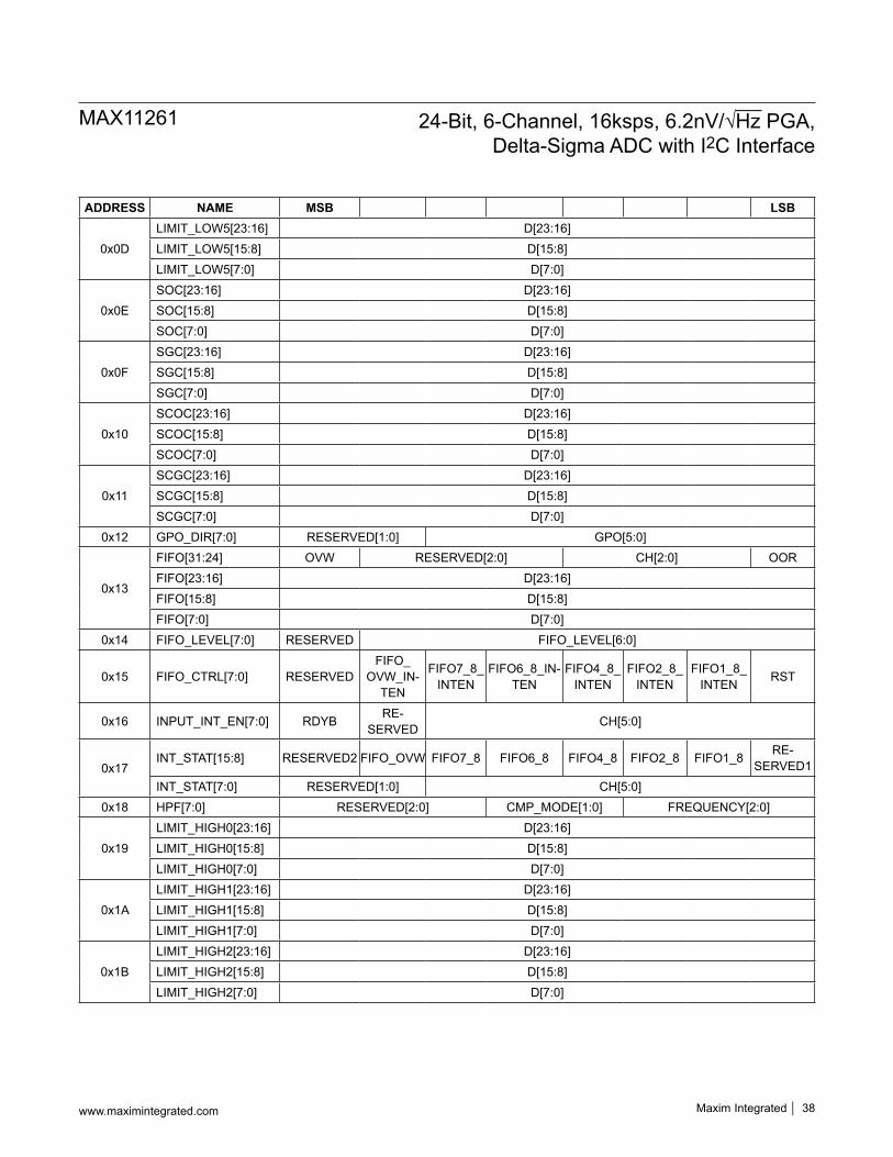
ADDRESS NAME MSB LSB
0x0DLIMIT_LOW5[23:16] D[23:16]LIMIT_LOW5[15:8] D[15:8]LIMIT_LOW5[7:0] D[7:0]
0x0ESOC[23:16] D[23:16]SOC[15:8] D[15:8]SOC[7:0] D[7:0]
0x0FSGC[23:16] D[23:16]SGC[15:8] D[15:8]SGC[7:0] D[7:0]
0x10SCOC[23:16] D[23:16]SCOC[15:8] D[15:8]SCOC[7:0] D[7:0]
0x11SCGC[23:16] D[23:16]SCGC[15:8] D[15:8]SCGC[7:0] D[7:0]
0x12 GPO_DIR[7:0] RESERVED[1:0] GPO[5:0]
0x13
FIFO[31:24] OVW RESERVED[2:0] CH[2:0] OORFIFO[23:16] D[23:16]FIFO[15:8] D[15:8]FIFO[7:0] D[7:0]
0x14 FIFO_LEVEL[7:0] RESERVED FIFO_LEVEL[6:0]
0x15 FIFO_CTRL[7:0] RESERVEDFIFO_
OVW_IN-TEN
FIFO7_8_INTEN
FIFO6_8_IN-TEN
FIFO4_8_INTEN
FIFO2_8_INTEN
FIFO1_8_INTEN RST
0x16 INPUT_INT_EN[7:0] RDYB RE-SERVED CH[5:0]
0x17INT_STAT[15:8] RESERVED2 FIFO_OVW FIFO7_8 FIFO6_8 FIFO4_8 FIFO2_8 FIFO1_8 RE-
SERVED1INT_STAT[7:0] RESERVED[1:0] CH[5:0]
0x18 HPF[7:0] RESERVED[2:0] CMP_MODE[1:0] FREQUENCY[2:0]
0x19LIMIT_HIGH0[23:16] D[23:16]LIMIT_HIGH0[15:8] D[15:8]LIMIT_HIGH0[7:0] D[7:0]
0x1ALIMIT_HIGH1[23:16] D[23:16]LIMIT_HIGH1[15:8] D[15:8]LIMIT_HIGH1[7:0] D[7:0]
0x1BLIMIT_HIGH2[23:16] D[23:16]LIMIT_HIGH2[15:8] D[15:8]LIMIT_HIGH2[7:0] D[7:0]
www.maximintegrated.com Maxim Integrated │ 38
MAX11261 24-Bit, 6-Channel, 16ksps, 6.2nV/√Hz PGA, Delta-Sigma ADC with I2C Interface

ADDRESS NAME MSB LSB
0x1CLIMIT_HIGH3[23:16] D[23:16]LIMIT_HIGH3[15:8] D[15:8]LIMIT_HIGH3[7:0] D[7:0]
0x1DLIMIT_HIGH4[23:16] D[23:16]LIMIT_HIGH4[15:8] D[15:8]LIMIT_HIGH4[7:0] D[7:0]
0x1ELIMIT_HIGH5[23:16] D[23:16]LIMIT_HIGH5[15:8] D[15:8]LIMIT_HIGH5[7:0] D[7:0]
Register DetailsSTAT (0x0)Status Register (Read)
BIT 23 22 21 20 19 18 17 16Field RESERVED INRESET SRDY[5:0]Reset 0b0 0b0 0b000000Access Type Read Only Read Only Read Only
Bit 15 14 13 12 11 10 9 8Field SCANERR REFDET ORDERR GPOERR ERROR SYSGOR DOR AORReset 0b0 0b0 0b0 0b0 0b0 0b0 0b0 0b0Access Type Read Only Read Only Read Only Read Only Read Only Read Only Read Only Read Only
Bit 7 6 5 4 3 2 1 0Field RATE[3:0] PDSTAT[1:0] MSAT RDYReset 0x0 0b00 0b0 0b0Access Type Read Only Read Only Read Only Read Only
BITFIELD BITS DESCRIPTIONRESERVED 23 ReservedINRESET 22 This bit indicates the status of a reset command.
SRDY 21:16
For sequencer modes 2, 3, and 4, this bit when set to ‘1’ indicates that a new conversion result is available from the channel indicated by the SRDY bit position. A complete read of the FIFO register associated with the SRDY bit will reset the bit to ‘0’. At the start of a scan mode these bits are reset to ‘0’.
SCANERR 15Flag is set if the sequencer scan mode is enabled (mode 2, 3, or 4) and no channels or invalid channel numbers (3’b110, 3’b111) are enabled in the CHMAP1 or CHMAP2 regis-ter. Until SCANERR is cleared, CONVERSION commands are aborted.
www.maximintegrated.com Maxim Integrated │ 39
MAX11261 24-Bit, 6-Channel, 16ksps, 6.2nV/√Hz PGA, Delta-Sigma ADC with I2C Interface

BITFIELD BITS DESCRIPTION
REFDET 14
This bit is a ‘1’ if a proper reference voltage is detected and ‘0’ if a proper reference voltage is missing. In SLEEP or STANDBY the value of this bit is ‘0’. The trigger level for this bit is VREF < 0.35V. This error does not inhibit normal operation and is intended for status only. This flag is only valid during a conversion in progress and if the user needs to verify valid reference level they should read this status bit. The value of this status bit is valid within 30μs after a conversion start command and is invalid when not in conversion.
ORDERR 13
This bit is not valid in sequencer mode 1. Flag is set if two or more CHX_ORD bits decode to the same scan sequence order and are also enabled. This bit is also set for the case when a channel is enabled for scan with CHX_EN=’1’ and CHX_ORD[2:0] = ‘000’ or ‘111’. The CHX_ORD[2:0] values of ‘000’ and ‘111’ are not allowed for the order of an enabled channel. The allowable orders are 1, 2, 3, 4, 5, 6. The MAX11261 remains in STANDBY state until this error is removed. The channel order must be strictly sequen-tial and no missing numbers are allowed. For instance, if 4 channels are enabled then the order must be 1, 2, 3, 4. Any other order is flagged as ORDERR and the MAX11261 remains in STANDBY mode.
GPOERR 12This bit is not valid in sequencer mode 1. This bit is set to ‘1’ if more than one input chan-nel is mapped to the same GPO bump, and CHX_GPOEN is enabled for more than one channel. The MAX11261 remains in STANDBY state until this error is removed.
ERROR 11Flag for invalid configuration states. Flag is set if CAL[1:0] programmed to ‘11’ which is an invalid state. Flag is set if CTRL1:SCYCLE = ‘0’ for scan modes 2, 3, and 4. This error puts the MAX11261 into STANDBY mode.
SYSGOR 10This bit when set to ‘1’ indicates that a system gain calibration was overrange. The SCGC calibration coefficient is the maximum value of 1.9999999. This bit when set to ‘1’ indi-cates that full-scale value out of the converter is likely not available.
DOR 9This bit when set to ‘1’ indicates that the conversion result has exceeded the maximum or minimum value of the converter and that the result has been clipped or limited to the maximum value. When ‘0’ the conversion result is within the full-scale range of the inputs.
AOR 8This bit indicates if the modulator detected an analog overrange condition from having the input signal level greater than the reference voltage. This check for overrange includes the PGA.
RATE 7:4These bits indicate the conversion rate that corresponds to the result in the FIFO reg-ister or the rate that was used for calibration coefficient calculation. The corresponding RATE[3:0] is only valid until the FIFO register is read.
PDSTAT 3:2
These bits indicate the power-down state of the chip. See Table 5 for transition times.‘00’ = CONVERSION‘01’ = SLEEP‘10’ = STANDBY (default)‘11’ = RESET
MSAT 1This bit is set to ‘1’ when a signal measurement is in progress. This indicates that a conversion, self-calibration, or system calibration is in progress and that the modulator is busy. When the modulator is not converting, this bit will be set to ‘0’.
RDY 0
For sequencer mode 1, this bit when set to ‘1’ indicates that a new conversion result is available. A complete read of the FIFO Register will reset this bit to ‘0’. This bit is invalid in sequencer mode 2, 3, or 4. The function of this bit is redundant and is duplicated by the RDYB_INTB pin.
www.maximintegrated.com Maxim Integrated │ 40
MAX11261 24-Bit, 6-Channel, 16ksps, 6.2nV/√Hz PGA, Delta-Sigma ADC with I2C Interface

CTRL1 (0x1)Control Register 1 (Read/Write)This register controls the selection of operational modes and configurations.
BIT 7 6 5 4 3 2 1 0Field CAL[1:0] PD[1:0] U_B FORMAT SCYCLE CONTSCReset 0b00 0b00 0b0 0b0 0b1 0b0Access Type Write, Read Write, Read Write, Read Write, Read Write, Read Write, Read
BITFIELD BITS DESCRIPTION
CAL 7:6
Calibration bits control the type of calibration performed when the calibration command byte is issued. Selects the type of calibration to perform.‘00’ = Performs a self-calibration.‘01’ = Performs a system-level offset calibration.‘10’ = Performs a system-level full-scale calibration.‘11’ = Not used, reserved state.
PD 5:4
Selects the power-down state to be executed. The MAX11261 enters the selected power-down state after the IMPD is written. These bits are decoded below:‘00’ = NOP (default)‘01’ = SLEEP‘10’ = STANDBY‘11’ = RESET
U_B 3 The ‘unipolar/bipolar’ bit controls the input range. A ‘1’ selects unipolar input range and a ‘0’ selects bipolar input range.
FORMAT 2
The ‘format’ bit controls the digital format of the bipolar range data. A ‘0’ selects two’s complement and a ‘1’ selects offset binary format of the bipo-lar range. The data from unipolar range is always formatted in offset binary format. The value of the format must be ‘0’ when operating sequencer mode 4, incorrect results are obtained when ‘1’.
SCYCLE 1
The ‘single-cycle’ bit selects either no-latency single conversion mode or latent continuous conversion in sequencer mode 1. A ‘1’ selects single-cycle mode where a no-latency conversion is followed by a power-down to SLEEP state. A ‘0’ selects continuous conversion mode with a latency of 5 conver-sion cycles for filtering and the RDYB pin goes low when valid/settled data is available.Only SCYCLE = ‘1’ is valid in sequencer mode 2, 3, and 4. Set SCYCLE to 0 in mode 2, 3, and 4 will flag ERROR and put the device in STANDBY mode.
CONTSC 0
The ‘continuous single-cycle’ bit selects between single or continuous conver-sions while operating in single-cycle mode in sequencer mode 1. A ‘1’ selects continuous conversions and a ‘0’ selects single conversion.CONTSC is ignored in mode 2, 3, and 4.
www.maximintegrated.com Maxim Integrated │ 41
MAX11261 24-Bit, 6-Channel, 16ksps, 6.2nV/√Hz PGA, Delta-Sigma ADC with I2C Interface
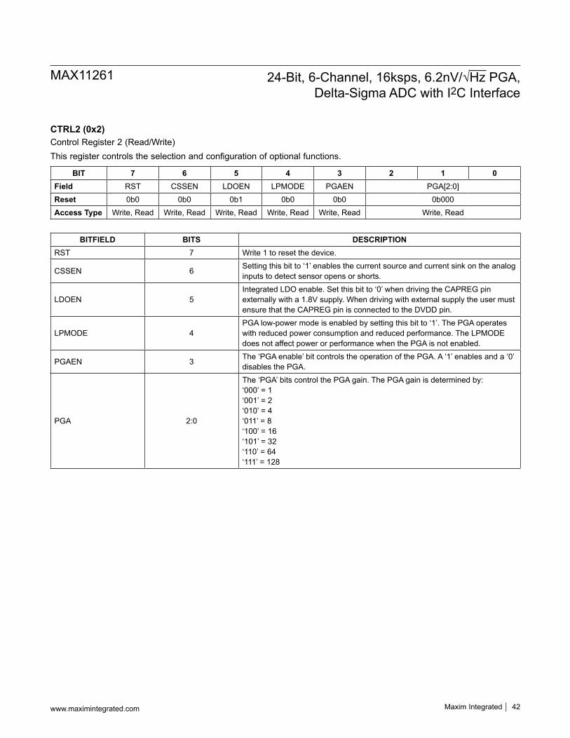
CTRL2 (0x2)Control Register 2 (Read/Write)This register controls the selection and configuration of optional functions.
BIT 7 6 5 4 3 2 1 0Field RST CSSEN LDOEN LPMODE PGAEN PGA[2:0]Reset 0b0 0b0 0b1 0b0 0b0 0b000Access Type Write, Read Write, Read Write, Read Write, Read Write, Read Write, Read
BITFIELD BITS DESCRIPTIONRST 7 Write 1 to reset the device.
CSSEN 6 Setting this bit to ‘1’ enables the current source and current sink on the analog inputs to detect sensor opens or shorts.
LDOEN 5Integrated LDO enable. Set this bit to ‘0’ when driving the CAPREG pin externally with a 1.8V supply. When driving with external supply the user must ensure that the CAPREG pin is connected to the DVDD pin.
LPMODE 4PGA low-power mode is enabled by setting this bit to ‘1’. The PGA operates with reduced power consumption and reduced performance. The LPMODE does not affect power or performance when the PGA is not enabled.
PGAEN 3 The ‘PGA enable’ bit controls the operation of the PGA. A ‘1’ enables and a ‘0’ disables the PGA.
PGA 2:0
The ‘PGA’ bits control the PGA gain. The PGA gain is determined by:‘000’ = 1‘001’ = 2‘010’ = 4‘011’ = 8‘100’ = 16‘101’ = 32‘110’ = 64‘111’ = 128
www.maximintegrated.com Maxim Integrated │ 42
MAX11261 24-Bit, 6-Channel, 16ksps, 6.2nV/√Hz PGA, Delta-Sigma ADC with I2C Interface

CTRL3 (0x3)Control Register 3 (Read/Write)This register is used to control the operation and calibration of the MAX11261.
BIT 7 6 5 4 3 2 1 0
Field RESERVED SYNCZ SYNC CALREG-SEL NOSYSG NOSYSO NOSCG NOSCO
Reset 0b0 0b1 0b1 0b1 0b1 0b1 0b0 0b0Access Type Write, Read Write, Read Write, Read Write, Read Write, Read Write, Read Write, Read Write, Read
BITFIELD BITS DESCRIPTIONRESERVED 7 Reserved
SYNCZ 6In sequencer mode 4, when CTRL3:SYNC is set high (the device is a master), set CTRL3:SYNCZ high to put SYNC pin in high impedance state. Set CTRL3:SYNCZ low to put SYNC pin in active-low, open-drain output state.
SYNC 5 Set this bit to 1 to configure the device as a master device.
CALREGSEL 4
The value of this bit controls which calibration value is read during a calibration register inquiry. When the user writes into one of the calibration registers the value is stored within the interface domain. Once a command to convert is received, the new calibration value is transferred to a MATH module in a separate digital domain to be used in any valid calibration sequence. The user has access to both registers, i.e. the register value that was used to produce the current conversion result in the FIFO register or the value that was just written and is meant to be used for following conversions.It is common for a user to immediately read back the value written to insure that com-munication was not flawed. To accomplish this, set the CTRL3:CALREGSEL bit to ‘1’ in order to read back the interface value of the register. Set this bit to ‘0’ to read the MATH module value, i.e. the value used to generate the result in the FIFO register.Note that when CTRL3:CALREGSEL is ‘0’ only read operations are valid.
NOSYSG 3
The ‘no system gain’ bit controls the use of the system gain calibration coefficient. A ‘1’ in this location disables the use of the system gain value when computing the final offset and gain corrected data value. A ‘0’ in this location enables the use of the system gain value when computing the final offset and gain corrected data value.
NOSYSO 2
The ‘no system offset’ bit controls the use of the system offset calibration coefficient. A ‘‘1’ in this location disables the use of the system offset value when computing the final offset and gain corrected data value. A ‘‘0’ in this location enables the use of the system offset value when computing the final offset and gain corrected data value.
NOSCG 1
The ‘no self-calibration gain’ bit controls the use of the self-calibration gain calibration coefficient. A ‘1’ in this location disables the use of the self-calibration gain value when computing the final offset and gain corrected data value. A ‘0’ in this location enables the use of the self-calibration gain value when computing the final offset and gain corrected data value.
NOSCO 0
The ‘no self-calibration offset’ bit controls the use of the self-calibration offset calibration coefficient. A ‘1’ in this location disables the use of the self-calibration offset value when computing the final offset and gain corrected data value. A ‘0’ in this location enables the use of the self-calibration offset value when computing the final offset and gain corrected data value.
www.maximintegrated.com Maxim Integrated │ 43
MAX11261 24-Bit, 6-Channel, 16ksps, 6.2nV/√Hz PGA, Delta-Sigma ADC with I2C Interface

SEQ (0x4)Sequencer Register (Read/Write)This register is used to control the operation of the sequencer when enabled.
BIT 15 14 13 12 11 10 9 8Field MUX[2:0] MODE[1:0] GPODREN MDREN RDYBENReset 0b000 0b00 0b0 0b0 0b0Access Type Write, Read Write, Read Write, Read Write, Read Write, Read Bit 7 6 5 4 3 2 1 0Field RESERVED[5:0] SIF_FREQ[1:0]Reset 0x00 0b01Access Type Write, Read Write, Read
BITFIELD BITS DESCRIPTION
MUX 15:13 Binary channel selection for sequencer mode 1. Valid channels are from 3’b000 (channel 0) to 3’b101 (channel 5).
MODE 12:11
Sequencer mode is decoded as shown in the following table:MODE1 MODE0 DESCRIPTION
0 0 Sequencer Mode 1
0 1 Sequencer Mode 21 0 Sequencer Mode 31 1 Sequencer Mode 4
GPODREN 10 GPO delay enable. Enables operation of the GPO switch delay. When enabled, the channel selection is delayed. The value of the delay is set by the DELAY:GPO bits.
MDREN 9 MUX delay enable. Enables the timer setting in DELAY:MUX register to delay the conversion start of the selected channel.
RDYBEN 8 Ready Bar enable. When this bit is ‘1’ the RDYB is inhibited from asserting in sequencer mode 2 and 3 until all channels are converted
RESERVED 7:2 Reserved
SIF_FREQ 1:0
The register SIF_FREQ[1:0] configures the internal FIFO clock according to the serial interface clock speed at which the FIFO register is being read.
Before reading the FIFO register at a different serial clock speed range, set SIF_FREQ[1:0] accordingly.
SIF_FREQ1 SIF_FREQ0 SERIAL CLOCK SPEED0 0 100 kHz ≤ speed ≤ 400 kHz0 1 400 kHz < speed ≤ 1 MHz1 0 1 MHz < speed ≤ 3 MHz1 1 3 MHz < speed ≤ 5 MHz
www.maximintegrated.com Maxim Integrated │ 44
MAX11261 24-Bit, 6-Channel, 16ksps, 6.2nV/√Hz PGA, Delta-Sigma ADC with I2C Interface

CHMAP1 (0x5)Channel Map Register (Read/Write)These registers are used to enable channels for scan, enable output controls for scan, program the channel scan order, and pair the GPO bumps with its associated channel. These registers cannot be written during an active conversion.
BIT NAME DESCRIPTION
CHX_GPO[2:0] Used to map which GPO bump is activated when this channel is selected. The STAT:GPOERR flag is set if two or more output controls are mapped to the same channel.
CHX_ORD[2:0]
Used to define the order during scan when the channel is enabled. The CHX_ORD[2:0] values of ‘000’ and ‘111’ are not allowed for the order of an enabled channel. The allowable orders are 1, 2, 3, 4, 5, and 6 rep-resenting first, second, third, and so on. The value of ‘000’ is a default value and the value of ‘111’ is greater than the number of scannable channels. A value greater than the number of scannable channels is invalid and will set an error condition at STAT:ORDERR. Setting a channels order to ‘000’ or ‘111’ and enabling it will set the STAT:ORDERR flag in the STAT register.
CHX_EN Used to enable this channel for scan.CHX_GPOEN Used to enable activation of the GPO bump when this channel is selected during scan.
BIT 23 22 21 20 19 18 17 16Field CH5_GPO[2:0] CH5_ORD[2:0] CH5_EN CH5_GPOENReset 0b000 0b000 0b0 0b0Access Type Write, Read Write, Read Write, Read Write, Read
Bit 15 14 13 12 11 10 9 8Field CH4_GPO[2:0] CH4_ORD[2:0] CH4_EN CH4_GPOENReset 0b000 0b000 0b0 0b0Access Type Write, Read Write, Read Write, Read Write, Read
Bit 7 6 5 4 3 2 1 0Field CH3_GPO[2:0] CH3_ORD[2:0] CH3_EN CH3_GPOENReset 0b000 0b000 0b0 0b0Access Type Write, Read Write, Read Write, Read Write, Read
BITFIELD BITS DESCRIPTIONCH5_GPO 23:21CH5_ORD 20:18CH5_EN 17CH5_GPOEN 16CH4_GPO 15:13CH4_ORD 12:10CH4_EN 9CH4_GPOEN 8CH3_GPO 7:5CH3_ORD 4:2CH3_EN 1CH3_GPOEN 0
www.maximintegrated.com Maxim Integrated │ 45
MAX11261 24-Bit, 6-Channel, 16ksps, 6.2nV/√Hz PGA, Delta-Sigma ADC with I2C Interface

CHMAP0 (0x6)Channel Map Register (Read/Write)
BIT 23 22 21 20 19 18 17 16Field CH2_GPO[2:0] CH2_ORD[2:0] CH2_EN CH2_GPOENReset 0b000 0b000 0b0 0b0Access Type Write, Read Write, Read Write, Read Write, Read
Bit 15 14 13 12 11 10 9 8Field CH1_GPO[2:0] CH1_ORD[2:0] CH1_EN CH1_GPOENReset 0b000 0b000 0b0 0b0Access Type Write, Read Write, Read Write, Read Write, Read
Bit 7 6 5 4 3 2 1 0Field CH0_GPO[2:0] CH0_ORD[2:0] CH0_EN CH0_GPOENReset 0b000 0b000 0b0 0b0Access Type Write, Read Write, Read Write, Read Write, Read
BITFIELD BITS DESCRIPTIONCH2_GPO 23:21CH2_ORD 20:18CH2_EN 17CH2_GPOEN 16CH1_GPO 15:13CH1_ORD 12:10CH1_EN 9CH1_GPOEN 8CH0_GPO 7:5CH0_ORD 4:2CH0_EN 1CH0_GPOEN 0
www.maximintegrated.com Maxim Integrated │ 46
MAX11261 24-Bit, 6-Channel, 16ksps, 6.2nV/√Hz PGA, Delta-Sigma ADC with I2C Interface

DELAY (0x7)Delay Register (Read/Write)
BIT 23 22 21 20 19 18 17 16Field AUTOSCAN[7:0]Reset 0x01Access Type Write, Read
Bit 15 14 13 12 11 10 9 8Field MUX[7:0]Reset 0x00Access Type Write, Read
Bit 7 6 5 4 3 2 1 0Field GPO[7:0]Reset 0x00Access Type Write, Read
BITFIELD BITS DESCRIPTION
AUTOSCAN 23:16Used to program the autoscan delay. The autoscan delay ranges from 4ms to 1.024s. The default value of 0x00 corresponds to no delay.The timer resolu-tion is 4ms.
MUX 15:8 Used to program the mux delay. The mux delay ranges from 4μs to 1.024ms. The default value of 0x00 corresponds to no delay. The timer resolution is 4μs.
GPO 7:0 Used to program the GPO delay. The GPO delay ranges from 20μs to 5.1ms. The default value of 0x00 corresponds to no delay. 1 LSB = 20μs of delay.
www.maximintegrated.com Maxim Integrated │ 47
MAX11261 24-Bit, 6-Channel, 16ksps, 6.2nV/√Hz PGA, Delta-Sigma ADC with I2C Interface

LIMIT_LOW0 (0x8)This register stores the lower limit value for channel 0. It sets the lower bound for the comparitor.
BIT 23 22 21 20 19 18 17 16Field D[23:16]Reset 0x000000Access Type Write, Read
Bit 15 14 13 12 11 10 9 8Field D[15:8]Reset 0x000000Access Type Write, Read
Bit 7 6 5 4 3 2 1 0Field D[7:0]Reset 0x000000Access Type Write, Read
BITFIELD BITS DESCRIPTIOND 23:0
LIMIT_LOW1 (0x9)This register stores the lower limit value for channel 1. It sets the lower bound for the comparitor.
BIT 23 22 21 20 19 18 17 16Field D[23:16]Reset 0x000000Access Type Write, Read
Bit 15 14 13 12 11 10 9 8Field D[15:8]Reset 0x000000Access Type Write, Read
Bit 7 6 5 4 3 2 1 0Field D[7:0]Reset 0x000000Access Type Write, Read
BITFIELD BITS DESCRIPTIOND 23:0
www.maximintegrated.com Maxim Integrated │ 48
MAX11261 24-Bit, 6-Channel, 16ksps, 6.2nV/√Hz PGA, Delta-Sigma ADC with I2C Interface
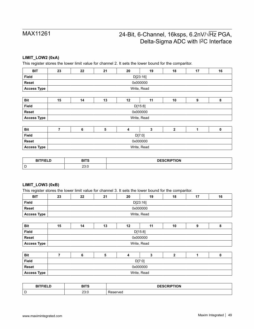
LIMIT_LOW2 (0xA)This register stores the lower limit value for channel 2. It sets the lower bound for the comparitor.
BIT 23 22 21 20 19 18 17 16Field D[23:16]Reset 0x000000Access Type Write, Read
Bit 15 14 13 12 11 10 9 8Field D[15:8]Reset 0x000000Access Type Write, Read
Bit 7 6 5 4 3 2 1 0Field D[7:0]Reset 0x000000Access Type Write, Read
BITFIELD BITS DESCRIPTIOND 23:0
LIMIT_LOW3 (0xB)This register stores the lower limit value for channel 3. It sets the lower bound for the comparitor.
BIT 23 22 21 20 19 18 17 16Field D[23:16]Reset 0x000000Access Type Write, Read
Bit 15 14 13 12 11 10 9 8Field D[15:8]Reset 0x000000Access Type Write, Read
Bit 7 6 5 4 3 2 1 0Field D[7:0]Reset 0x000000Access Type Write, Read
BITFIELD BITS DESCRIPTIOND 23:0 Reserved
www.maximintegrated.com Maxim Integrated │ 49
MAX11261 24-Bit, 6-Channel, 16ksps, 6.2nV/√Hz PGA, Delta-Sigma ADC with I2C Interface

LIMIT_LOW4 (0xC)This register stores the lower limit value for channel 4. It sets the lower bound for the comparitor.
BIT 23 22 21 20 19 18 17 16Field D[23:16]Reset 0x000000Access Type Write, Read
Bit 15 14 13 12 11 10 9 8Field D[15:8]Reset 0x000000Access Type Write, Read
Bit 7 6 5 4 3 2 1 0Field D[7:0]Reset 0x000000Access Type Write, Read
BITFIELD BITS DESCRIPTIOND 23:0
LIMIT_LOW5 (0xD)This register stores the lower limit value for channel 5. It sets the lower bound for the comparitor.
BIT 23 22 21 20 19 18 17 16Field D[23:16]Reset 0x000000Access Type Write, Read
Bit 15 14 13 12 11 10 9 8Field D[15:8]Reset 0x000000Access Type Write, Read
Bit 7 6 5 4 3 2 1 0Field D[7:0]Reset 0x000000Access Type Write, Read
BITFIELD BITS DESCRIPTIOND 23:0
www.maximintegrated.com Maxim Integrated │ 50
MAX11261 24-Bit, 6-Channel, 16ksps, 6.2nV/√Hz PGA, Delta-Sigma ADC with I2C Interface

SOC (0xE)System Offset Calibration Register (Read/Write)The System Offset Calibration register is a 24-bit read/write register. The data written/read to/from this register is clocked in/out MSB first. This register holds the system offset calibration value. The format is in two’s complement binary format. An internal system calibration does not overwrite the SOC register.The readback value of this register depends on CTRL3:CALREGSEL. A ‘1’ reads back the user programmed value. A ‘0’ reads back the results of an internal register as described in CTRL3 for bit CALREGSEL. The internal register can only be read during conversion.The system offset calibration value is subtracted from each conversion result—provided the NOSYSO bit in the CTRL3 register is set to 0. The system offset calibration value is subtracted from the conversion result after self-calibration but before system gain correction. It is also applied prior to the 1x or 2x scale factor associated with bipolar and unipolar modes. When a system offset calibration is in progress, this register is not writable by the user.
BIT 23 22 21 20 19 18 17 16Field D[23:16]Reset 0x000000Access Type Write, Read
Bit 15 14 13 12 11 10 9 8Field D[15:8]Reset 0x000000Access Type Write, Read
Bit 7 6 5 4 3 2 1 0Field D[7:0]Reset 0x000000Access Type Write, Read
BITFIELD BITS DESCRIPTIOND 23:0
www.maximintegrated.com Maxim Integrated │ 51
MAX11261 24-Bit, 6-Channel, 16ksps, 6.2nV/√Hz PGA, Delta-Sigma ADC with I2C Interface

SGC (0xF)System Gain Calibration Register(Read/Write)The System Gain Calibration register is a 24-bit read/write register. The data written/read to/from this register is clocked in/out MSB first. This register holds the system gain calibration value. The format is unsigned 24-bit binary. An internal system calibration does not overwrite the SGC register.The readback value of this register depends on CTRL3:CALREGSEL. A ‘1’ reads back the user programmed value. A ‘0’ reads back the results of an internal register as described in CTRL3 for bit CALREGSEL. The internal register can only be read during conversion.The system gain calibration value is used to scale the offset corrected conversion result—provided the NOSYSG bit in the CTRL3 register is set to 0. The system gain calibration value scales the offset corrected result by up to 2x or can correct a gain error of approximately -50%. The amount of positive gain error that can be corrected is determined by modulator overload characteristics, which may be as much as +25%. When a system gain calibration is in progress, this register is not writable by the user.
BIT 23 22 21 20 19 18 17 16Field D[23:16]Reset 0x7FFFFFAccess Type Write, Read
Bit 15 14 13 12 11 10 9 8Field D[15:8]Reset 0x7FFFFFAccess Type Write, Read
Bit 7 6 5 4 3 2 1 0Field D[7:0]Reset 0x7FFFFFAccess Type Write, Read
BITFIELD BITS DESCRIPTIOND 23:0
www.maximintegrated.com Maxim Integrated │ 52
MAX11261 24-Bit, 6-Channel, 16ksps, 6.2nV/√Hz PGA, Delta-Sigma ADC with I2C Interface

SCOC (0x10)Self-Calibration Offset Calibration Register (Read/Write)The self-calibration offset register is a 24-bit read/write register. The data written/read to/from this register is clocked in/out MSB first. This register holds the self-calibration offset value. The format is always in two’s complement binary format. An internal self- calibration does not overwrite the SCOC register.The readback value of this register depends on CTRL3:CALREGSEL. A ‘1’ reads back the user programmed value. A ‘0’ reads back the results of an internal register as described in CTRL3 for bit CALREGSEL. The internal register can only be read during conversion.The self-calibration offset value is subtracted from each conversion result—provided the NOSCO bit in the CTRL3 reg-ister is set to 0. The self-calibration offset value is subtracted from the conversion result before the self-calibration gain correction and before the system offset and gain correction. It is also applied prior to the 2x scale factor associated with unipolar mode. When a self-calibration is in progress, this register is not writable by the user.
BIT 23 22 21 20 19 18 17 16Field D[23:16]Reset 0x000000Access Type Write, Read
Bit 15 14 13 12 11 10 9 8Field D[15:8]Reset 0x000000Access Type Write, Read
Bit 7 6 5 4 3 2 1 0Field D[7:0]Reset 0x000000Access Type Write, Read
BITFIELD BITS DESCRIPTIOND 23:0
www.maximintegrated.com Maxim Integrated │ 53
MAX11261 24-Bit, 6-Channel, 16ksps, 6.2nV/√Hz PGA, Delta-Sigma ADC with I2C Interface

SCGC (0x11)Self-Calibration Gain Calibration Register (Read/Write)The Self-Calibration Offset register is a 24-bit read/write register. The data written/read to/from this register is clocked in/out MSB first. This register holds the self-calibration offset value. The format is always in two’s complement binary format. An internal self- calibration does not overwrite the SCGC register.The readback value of this register depends on CTRL3:CALREGSEL. A ‘1’ reads back the user programmed value. A ‘0’ reads back the results of an internal register as described in CTRL3 for bit CALREGSEL. The internal register can only be read during conversion.The self-calibration gain calibration value is used to scale the self-calibration offset corrected conversion result before the system offset and gain calibration values have been applied – provided the NOSCG bit in the CTRL3 register is set to 0. The self-calibration gain calibration value scales the self-calibration offset corrected conversion result by up to 2x or can correct a gain error of approximately –50%. The gain will be corrected to within 2 LSB. When a self- calibration is in progress, this register is not writable by the user.
BIT 23 22 21 20 19 18 17 16Field D[23:16]Reset 0xBF851BAccess Type Write, Read
Bit 15 14 13 12 11 10 9 8Field D[15:8]Reset 0xBF851BAccess Type Write, Read
Bit 7 6 5 4 3 2 1 0Field D[7:0]Reset 0xBF851BAccess Type Write, Read
BITFIELD BITS DESCRIPTIOND 23:0
GPO_DIR (0x12)GPO Direct Access Register (Read/Write)This register is used to turn on and off the GPO directly except when operating in mode 3 or mode 4. When operating in sequencer mode 1 or 2, the activation of the GPO is immediate upon setting a bit to a ‘1’ and the deactivation of the GPO is immediate upon setting the bit to a ‘0’. In SLEEP state, the values in this register do not control the state of the GPO as they all are deactivated. When in STANDBY state and programmed for sequencer mode 1 or mode 2, register writes immediately update the GPOs. Writes to this register are ignored when operating in sequencer mode 3 or mode 4. This register is used during system offset calibration, system gain calibration and self-calibration modes.
BIT 7 6 5 4 3 2 1 0Field RESERVED[1:0] GPO[5:0]Reset 0b00 0b000000Access Type Write, Read Write, Read
BITFIELD BITS DESCRIPTIONRESERVED 7:6 ReservedGPO 5:0
www.maximintegrated.com Maxim Integrated │ 54
MAX11261 24-Bit, 6-Channel, 16ksps, 6.2nV/√Hz PGA, Delta-Sigma ADC with I2C Interface

FIFO (0x13)FIFO Register (Read Only)The FIFO holds the most recent conversion results (up to a maximum of 64). If more than 64 conversions are captured and the user does not transfer the oldest FIFO entry, the oldest entry will be overwritten by the newest conversion result.The FIFO are read-only registers. Any attempt to write data to this location will have no effect. The data read from these registers is clocked out MSB first. The result D[23:0] is stored in a format according to the FORMAT bit in the CTRL1 register. The data format while in unipolar mode is always offset binary. In offset binary format the most negative value is 0x000000, the midscale value is 0x800000 and the most positive value is 0xFFFFFF. In bipolar mode if the FORMAT bit = ‘1’ then the data format is offset binary. If the FORMAT bit = ‘0’, then the data format is two’s complement. In two’s complement the negative full-scale value is 0x800000, the midscale is 0x000000 and the positive full scale is 0x7FFFFF. Any input exceeding the available input range is limited to the minimum or maximum data value.
BIT 31 30 29 28 27 26 25 24Field OVW RESERVED[2:0] CH[2:0] OORReset 0b0 0b000 0b000 0b0Access Type Read Only Read Only Read Only Read Only
Bit 23 22 21 20 19 18 17 16Field D[23:16]Reset 0x000000Access Type Read Only
Bit 15 14 13 12 11 10 9 8Field D[15:8]Reset 0x000000Access Type Read Only Bit 7 6 5 4 3 2 1 0Field D[7:0]Reset 0x000000Access Type Read Only
BITFIELD BITS DESCRIPTION
OVW 31 If this bit is set to 1, it indicates the previous FIFO entry overwrites the original data.
RESERVED 30:28 Reserved
CH 27:25 Channel ID. This registers represent the FIFO entry contains the result of the channel CH[2:0].
OOR 24 Out-of-range indication. If the channel's comparison result is out of the range set by LIMIT_LOWn and LIMIT_HIGHn registers, the OOR bit is set to 1.
D 23:0 The channels conversion result.
www.maximintegrated.com Maxim Integrated │ 55
MAX11261 24-Bit, 6-Channel, 16ksps, 6.2nV/√Hz PGA, Delta-Sigma ADC with I2C Interface
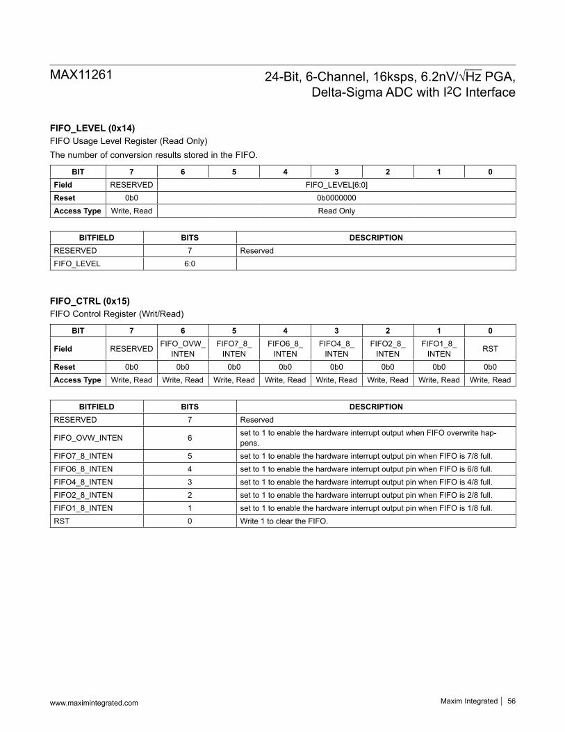
FIFO_LEVEL (0x14)FIFO Usage Level Register (Read Only)The number of conversion results stored in the FIFO.
BIT 7 6 5 4 3 2 1 0Field RESERVED FIFO_LEVEL[6:0]Reset 0b0 0b0000000Access Type Write, Read Read Only
BITFIELD BITS DESCRIPTIONRESERVED 7 ReservedFIFO_LEVEL 6:0
FIFO_CTRL (0x15)FIFO Control Register (Writ/Read)
BIT 7 6 5 4 3 2 1 0
Field RESERVED FIFO_OVW_INTEN
FIFO7_8_ INTEN
FIFO6_8_ INTEN
FIFO4_8_INTEN
FIFO2_8_ INTEN
FIFO1_8_INTEN RST
Reset 0b0 0b0 0b0 0b0 0b0 0b0 0b0 0b0Access Type Write, Read Write, Read Write, Read Write, Read Write, Read Write, Read Write, Read Write, Read
BITFIELD BITS DESCRIPTIONRESERVED 7 Reserved
FIFO_OVW_INTEN 6 set to 1 to enable the hardware interrupt output when FIFO overwrite hap-pens.
FIFO7_8_INTEN 5 set to 1 to enable the hardware interrupt output pin when FIFO is 7/8 full.FIFO6_8_INTEN 4 set to 1 to enable the hardware interrupt output pin when FIFO is 6/8 full.FIFO4_8_INTEN 3 set to 1 to enable the hardware interrupt output pin when FIFO is 4/8 full.FIFO2_8_INTEN 2 set to 1 to enable the hardware interrupt output pin when FIFO is 2/8 full.FIFO1_8_INTEN 1 set to 1 to enable the hardware interrupt output pin when FIFO is 1/8 full.RST 0 Write 1 to clear the FIFO.
www.maximintegrated.com Maxim Integrated │ 56
MAX11261 24-Bit, 6-Channel, 16ksps, 6.2nV/√Hz PGA, Delta-Sigma ADC with I2C Interface
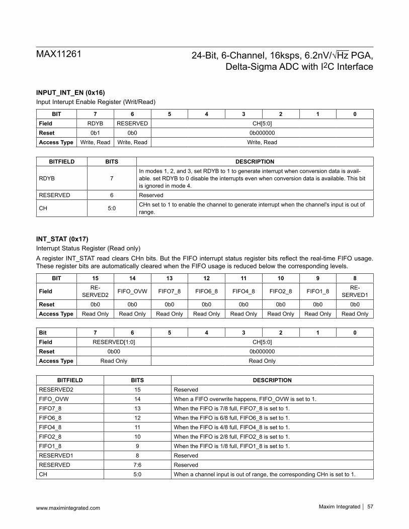
INPUT_INT_EN (0x16)Input Interupt Enable Register (Writ/Read)
BIT 7 6 5 4 3 2 1 0Field RDYB RESERVED CH[5:0]Reset 0b1 0b0 0b000000Access Type Write, Read Write, Read Write, Read
BITFIELD BITS DESCRIPTION
RDYB 7In modes 1, 2, and 3, set RDYB to 1 to generate interrupt when conversion data is avail-able. set RDYB to 0 disable the interrupts even when conversion data is available. This bit is ignored in mode 4.
RESERVED 6 Reserved
CH 5:0 CHn set to 1 to enable the channel to generate interrupt when the channel's input is out of range.
INT_STAT (0x17)Interrupt Status Register (Read only)A register INT_STAT read clears CHn bits. But the FIFO interrupt status register bits reflect the real-time FIFO usage. These register bits are automatically cleared when the FIFO usage is reduced below the corresponding levels.
BIT 15 14 13 12 11 10 9 8
Field RE-SERVED2 FIFO_OVW FIFO7_8 FIFO6_8 FIFO4_8 FIFO2_8 FIFO1_8 RE-
SERVED1Reset 0b0 0b0 0b0 0b0 0b0 0b0 0b0 0b0Access Type Read Only Read Only Read Only Read Only Read Only Read Only Read Only Read Only
Bit 7 6 5 4 3 2 1 0Field RESERVED[1:0] CH[5:0]Reset 0b00 0b000000Access Type Read Only Read Only
BITFIELD BITS DESCRIPTIONRESERVED2 15 ReservedFIFO_OVW 14 When a FIFO overwrite happens, FIFO_OVW is set to 1.FIFO7_8 13 When the FIFO is 7/8 full, FIFO7_8 is set to 1.FIFO6_8 12 When the FIFO is 6/8 full, FIFO6_8 is set to 1.FIFO4_8 11 When the FIFO is 4/8 full, FIFO4_8 is set to 1.FIFO2_8 10 When the FIFO is 2/8 full, FIFO2_8 is set to 1.FIFO1_8 9 When the FIFO is 1/8 full, FIFO1_8 is set to 1.RESERVED1 8 ReservedRESERVED 7:6 ReservedCH 5:0 When a channel input is out of range, the corresponding CHn is set to 1.
www.maximintegrated.com Maxim Integrated │ 57
MAX11261 24-Bit, 6-Channel, 16ksps, 6.2nV/√Hz PGA, Delta-Sigma ADC with I2C Interface

HPF (0x18)High-Pass Digital Filter Control Register (Write/Read)
BIT 7 6 5 4 3 2 1 0Field RESERVED[2:0] CMP_MODE[1:0] FREQUENCY[2:0]Reset 0b000 0b00 0b000Access Type Write, Read Write, Read Write, Read
BITFIELD BITS DESCRIPTION DECODERESERVED 7:5 Reserved
CMP_MODE 4:3Sets how input conversion results are used to generate the input activity indication and out-of-range bit.
0x0: use DATAn to compare with LIMIT_LOWn and LIMIT_HIGHn0x1: use DATAn - previous DATAn to compare with LIMIT_LOWn and LIMIT_HIGHn0x2: use high-pass filter output to compare with LIMIT_LOWn and LIMIT_HIGHn0x3: RESERVED
FREQUENCY 2:0 The HPF Cut-off Frequency (Hz)
0x0: Scan rate/39.06250x1: Scan rate/78.1250x2: Scan rate/156.250x3: scan rate/312.50x4: scan rate/6250x5: scan rate/12500x6: scan rate/25000x7: scan rate/5000
LIMIT_HIGH0 (0x19)This register stores the higher limit value for channel 0. It sets the upper bound for the comparitor.
BIT 23 22 21 20 19 18 17 16Field D[23:16]Reset 0x000000Access Type Write, Read
Bit 15 14 13 12 11 10 9 8Field D[15:8]Reset 0x000000Access Type Write, Read
Bit 7 6 5 4 3 2 1 0Field D[7:0]Reset 0x000000Access Type Write, Read
BITFIELD BITS DESCRIPTIOND 23:0
www.maximintegrated.com Maxim Integrated │ 58
MAX11261 24-Bit, 6-Channel, 16ksps, 6.2nV/√Hz PGA, Delta-Sigma ADC with I2C Interface

LIMIT_HIGH1 (0x1A)This register stores the higher limit value for channel 1. It sets the upper bound for the comparitor.
BIT 23 22 21 20 19 18 17 16Field D[23:16]Reset 0x000000Access Type Write, Read
Bit 15 14 13 12 11 10 9 8Field D[15:8]Reset 0x000000Access Type Write, Read
Bit 7 6 5 4 3 2 1 0Field D[7:0]Reset 0x000000Access Type Write, Read
BITFIELD BITS DESCRIPTIOND 23:0
LIMIT_HIGH2 (0x1B)This register stores the higher limit value for channel 2. It sets the upper bound for the comparitor.
BIT 23 22 21 20 19 18 17 16Field D[23:16]Reset 0x000000Access Type Write, Read
Bit 15 14 13 12 11 10 9 8Field D[15:8]Reset 0x000000Access Type Write, Read
Bit 7 6 5 4 3 2 1 0Field D[7:0]Reset 0x000000Access Type Write, Read
BITFIELD BITS DESCRIPTIOND 23:0
www.maximintegrated.com Maxim Integrated │ 59
MAX11261 24-Bit, 6-Channel, 16ksps, 6.2nV/√Hz PGA, Delta-Sigma ADC with I2C Interface

LIMIT_HIGH3 (0x1C)This register stores the higher limit value for channel 3. It sets the upper bound for the comparitor.
BIT 23 22 21 20 19 18 17 16Field D[23:16]Reset 0x000000Access Type Write, Read
Bit 15 14 13 12 11 10 9 8Field D[15:8]Reset 0x000000Access Type Write, Read
Bit 7 6 5 4 3 2 1 0Field D[7:0]Reset 0x000000Access Type Write, Read
BITFIELD BITS DESCRIPTIOND 23:0
LIMIT_HIGH4 (0x1D)This register stores the higher limit value for channel 4. It sets the upper bound for the comparitor.
BIT 23 22 21 20 19 18 17 16Field D[23:16]Reset 0x000000Access Type Write, Read
Bit 15 14 13 12 11 10 9 8Field D[15:8]Reset 0x000000Access Type Write, Read
Bit 7 6 5 4 3 2 1 0Field D[7:0]Reset 0x000000Access Type Write, Read
BITFIELD BITS DESCRIPTIOND 23:0
www.maximintegrated.com Maxim Integrated │ 60
MAX11261 24-Bit, 6-Channel, 16ksps, 6.2nV/√Hz PGA, Delta-Sigma ADC with I2C Interface

LIMIT_HIGH5 (0x1E)This register stores the higher limit value for channel 5. It sets the upper bound for the comparitor.
BIT 23 22 21 20 19 18 17 16Field D[23:16]Reset 0x000000Access Type Write, Read
Bit 15 14 13 12 11 10 9 8Field D[15:8]Reset 0x000000Access Type Write, Read
Bit 7 6 5 4 3 2 1 0Field D[7:0]Reset 0x000000Access Type Write, Read
BITFIELD BITS DESCRIPTIOND 23:0
www.maximintegrated.com Maxim Integrated │ 61
MAX11261 24-Bit, 6-Channel, 16ksps, 6.2nV/√Hz PGA, Delta-Sigma ADC with I2C Interface

Applications InformationConnecting an External 1.8V Supply to DVDD for Digital I/O and Digital CoreThe voltage range of the DVDD I/O supply is specified from 2.0V to 3.6V if the internal LDO is used to power the digital core. If a lower I/O supply voltage is desired, the internal LDO can be disabled, and DVDD and CAPREG can be connected together as shown in Figure 23. In this mode of operation, DVDD can vary from 1.7V to 2.0V. The internal LDO must be disabled by setting CTRL2:LDOEN to ‘0’.
Sensor Fault DetectionThe MAX11261 includes a 1μA current source and a 1μA current sink. The source pulls current from AVDD to AIN_P and sink from AIN_N to AVSS. The currents are enabled by register bit CTRL2:CSSEN. These currents are used to detect damaged sensors in either open or shorted state. The current sources and sinks are functional over the normal input operating voltage range, as specified.
These currents are used to test sensors for functional operation before taking measurements on that input channel. With the source and sink enabled, the currents flow into the external sensor circuit and measurement of the input voltage is used to diagnose sensor faults. A full-scale reading could indicate a sensor is open-circuit or overloaded or that the ADC’s reference is absent. If a zero-scale is read back, this may indicate the sensor is short-circuited.
PART TEMP RANGE
PIN- PACKAGE
MAX HEIGHT
MAX11261ENX+ -40°C to +85°C 36 WLP 0.5mm
+Denotes a lead(Pb)-free/RoHS-compliant package.T = Denotes tape-and-reel.
Figure 23. Application Diagram for 1.8V DVDD
MAX11261µC
1nFC0G
AIN5P
AIN5NGPO0
1nFC0G
GPO5
AIN0N
AIN0P
10nF
REFN REFP
1µF
AVDD
2.7V TO 3.6V
GPOGND CAPP CAPN
1nFC0G
CAPREG DGNDAVSS
RDYB_INTB
SDA
ADR1
SCL
ADR0
RESISTIVE BRIDGE MEASUREMENT CIRCUIT, I2C CONFIGURATION
DVDD
1.7V TO 2.0V
REF
RSTB
SYNC
1µF
Ordering Information
www.maximintegrated.com Maxim Integrated │ 62
MAX11261 24-Bit, 6-Channel, 16ksps, 6.2nV/√Hz PGA, Delta-Sigma ADC with I2C Interface

REVISIONNUMBER
REVISIONDATE DESCRIPTION PAGES
CHANGED0 2/18 Initial release —
Revision History
Maxim Integrated cannot assume responsibility for use of any circuitry other than circuitry entirely embodied in a Maxim Integrated product. No circuit patent licenses are implied. Maxim Integrated reserves the right to change the circuitry and specifications without notice at any time. The parametric values (min and max limits) shown in the Electrical Characteristics table are guaranteed. Other parametric values quoted in this data sheet are provided for guidance.
Maxim Integrated and the Maxim Integrated logo are trademarks of Maxim Integrated Products, Inc. © 2018 Maxim Integrated Products, Inc. │ 63
MAX11261 24-Bit, 6-Channel, 16ksps, 6.2nV/√Hz PGA, Delta-Sigma ADC with I2C Interface
For pricing, delivery, and ordering information, please contact Maxim Direct at 1-888-629-4642, or visit Maxim Integrated’s website at www.maximintegrated.com.