Embed Size (px)
Citation preview
BeMicro Max 10 Getting Started User Guide, Version 14.0 1
BeMicro Max 10FPGA Evaluation Kit
Getting Started User Guide
Table of Contents
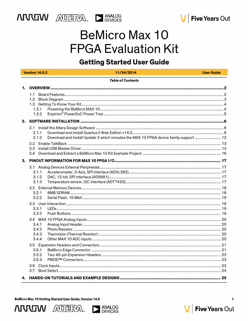
1. OVERVIEW ..................................................................................................................................................................2
1.1 Board Features..................................................................................................................................................................................... 21.2 Block Diagram ...................................................................................................................................................................................... 31.3 Getting To Know Your Kit.................................................................................................................................................................. 4
1.3.1 Powering the BeMicro MAX 10............................................................................................................................................. 41.3.2 Enpirion® PowerSoC Power Tree ......................................................................................................................................... 5
2. SOFTWARE INSTALLATION ......................................................................................................................................6
2.1 Install the Altera Design Software .................................................................................................................................................. 62.1.1 Download and Install Quartus II Web Edition v14.0........................................................................................................ 62.1.2 Download and Install Update 2 which includes the MAX 10 FPGA device family support .............................. 12
2.2 Enable TalkBack ............................................................................................................................................................................... 132.3 Install USB Blaster Driver ............................................................................................................................................................... 132.4 Download and Extract a BeMicro Max 10 Kit Example Project .......................................................................................... 16
3. PINOUT INFORMATION FOR MAX 10 FPGA I/O................................................................................................... 17
3.1 Analog Devices External Peripherals.......................................................................................................................................... 173.1.1 Accelerometer, 3-Axis, SPI interface (ADXL362) ......................................................................................................... 173.1.2 DAC, 12-bit, SPI interface (AD5681)................................................................................................................................ 173.1.3 Temperature sensor, I2C interface (ADT7420)............................................................................................................. 17
3.2 External Memory Devices............................................................................................................................................................... 183.2.1 8MB SDRAM ............................................................................................................................................................................ 183.2.2 Serial Flash, 16 Mbit .............................................................................................................................................................. 19
3.3 User Interaction................................................................................................................................................................................. 193.3.1 LEDs ........................................................................................................................................................................................... 193.3.2 Push Buttons ........................................................................................................................................................................... 19
3.4 MAX 10 FPGA Analog Inputs ........................................................................................................................................................ 203.4.1 Analog Input Header.............................................................................................................................................................. 203.4.2 Photo Resistor......................................................................................................................................................................... 203.4.3 Thermistor (Thermal Resistor) ............................................................................................................................................ 203.4.4 Other MAX 10 ADC inputs ................................................................................................................................................... 20
3.5 Expansion Headers and Connectors .......................................................................................................................................... 213.5.1 BeMicro Edge Connector .................................................................................................................................................... 213.5.2 Two 40-pin Expansion Headers ........................................................................................................................................ 223.5.3 PMOD™ Connectors............................................................................................................................................................. 23
3.6 Clock Inputs........................................................................................................................................................................................ 233.7 Boot Select ......................................................................................................................................................................................... 24
4. HANDS-ON TUTORIALS AND EXAMPLE DESIGNS .............................................................................................. 25
Version 14.0.2 11/24/2014 User Guide
BeMicro Max 10 Getting Started User Guide, Version 14.0 1
BeMicro Max 10FPGA Evaluation Kit
Getting Started User Guide
Table of Contents
1. OVERVIEW ..................................................................................................................................................................2
1.1 Board Features..................................................................................................................................................................................... 21.2 Block Diagram ...................................................................................................................................................................................... 31.3 Getting To Know Your Kit.................................................................................................................................................................. 4
1.3.1 Powering the BeMicro MAX 10............................................................................................................................................. 41.3.2 Enpirion® PowerSoC Power Tree ......................................................................................................................................... 5
2. SOFTWARE INSTALLATION ......................................................................................................................................6
2.1 Install the Altera Design Software .................................................................................................................................................. 62.1.1 Download and Install Quartus II Web Edition v14.0........................................................................................................ 62.1.2 Download and Install Update 2 which includes the MAX 10 FPGA device family support .............................. 12
2.2 Enable TalkBack ............................................................................................................................................................................... 132.3 Install USB Blaster Driver ............................................................................................................................................................... 132.4 Download and Extract a BeMicro Max 10 Kit Example Project .......................................................................................... 16
3. PINOUT INFORMATION FOR MAX 10 FPGA I/O................................................................................................... 17
3.1 Analog Devices External Peripherals.......................................................................................................................................... 173.1.1 Accelerometer, 3-Axis, SPI interface (ADXL362) ......................................................................................................... 173.1.2 DAC, 12-bit, SPI interface (AD5681)................................................................................................................................ 173.1.3 Temperature sensor, I2C interface (ADT7420)............................................................................................................. 17
3.2 External Memory Devices............................................................................................................................................................... 183.2.1 8MB SDRAM ............................................................................................................................................................................ 183.2.2 Serial Flash, 16 Mbit .............................................................................................................................................................. 19
3.3 User Interaction................................................................................................................................................................................. 193.3.1 LEDs ........................................................................................................................................................................................... 193.3.2 Push Buttons ........................................................................................................................................................................... 19
3.4 MAX 10 FPGA Analog Inputs ........................................................................................................................................................ 203.4.1 Analog Input Header.............................................................................................................................................................. 203.4.2 Photo Resistor......................................................................................................................................................................... 203.4.3 Thermistor (Thermal Resistor) ............................................................................................................................................ 203.4.4 Other MAX 10 ADC inputs ................................................................................................................................................... 20
3.5 Expansion Headers and Connectors .......................................................................................................................................... 213.5.1 BeMicro Edge Connector .................................................................................................................................................... 213.5.2 Two 40-pin Expansion Headers ........................................................................................................................................ 223.5.3 PMOD™ Connectors............................................................................................................................................................. 23
3.6 Clock Inputs........................................................................................................................................................................................ 233.7 Boot Select ......................................................................................................................................................................................... 24
4. HANDS-ON TUTORIALS AND EXAMPLE DESIGNS .............................................................................................. 25
Version 14.0.2 11/24/2014 User Guide
Overview
BeMicro Max 10 Getting Started User Guide, Version 14.0 2
1. OVERVIEW
BeMicro Max 10 is a FPGA evaluation kit that is designed to get you started with using an FPGA. BeMicro Max 10adopts Altera’s non-volatile MAX® 10 FPGA built on 55-nm flash process.
MAX 10 FPGAs revolutionize non-volatile integration by delivering advanced processing capabilities in a low-cost,instant-on, small form factor programmable logic device. The devices also include full-featured FPGA capabilitiessuch as digital signal processing, analog functionality, Nios II embedded processor support and memory controllers.
The BeMicro Max 10 includes a variety of peripherals connected to the FPGA device, such as 8MB SDRAM,accelerometer, digital-to-analog converter (DAC), temperature sensor, thermal resistor, photo resistor, LEDs,pushbuttons and several different options for expansion connectivity.
The kit retains the 80-pin edge connector interface used on previous Arrow BeMicro kits. Users can migrate theirdesigns from BeMicro SDK or BeMicro CV easily and take advantage of the new features Altera offers in the MAX 10FPGA device, such as an ADC block, temperature sense diode and flash memory.
1.1 Board Features
One MAX® 10 FPGA (10M08DAF484)o 8,000 LEso 414 Kbit (Kb) on-chip memoryo 256 Kbit (Kb) user flash memoryo 2 phase locked loops (PLLs)o 24 18x18-bit multiplierso 1 ADC block – 1 MSPS, 12-bit, 18-channelso 17 analog inputso 1 temperature sense diodeo 250 general purpose input/output (GPIO)o Non-volatile self-configuration with dual-boot support
Embedded USB-Blaster™ for use with the Quartus® II Programmer Clocking circuitry
o 50 MHz oscillator External peripherals
o 8MB SDRAM (4Mb x 16) (ISSI IS42S16400)o Accelerometer, 3-Axis, SPI interface (Analog Devices ADXL362)o DAC, 12-bit, SPI interface (Analog Devices AD5681)o Temperature sensor, I2C interface (Analog Devices ADT7420)o Thermal resistoro Photo resistor
General user input / outputo 8 user LEDs
Overview
BeMicro Max 10 Getting Started User Guide, Version 14.0 3
o 2 user Pushbuttons Prototyping
o Two 6-pin PMOD expansion headerso Two 40-pin prototyping headers which provide access to 64 digital I/Oo One 6-pin analog input headero One 80-pin BeMicro card edge connector
Power via USB or via user-provided 5V supply
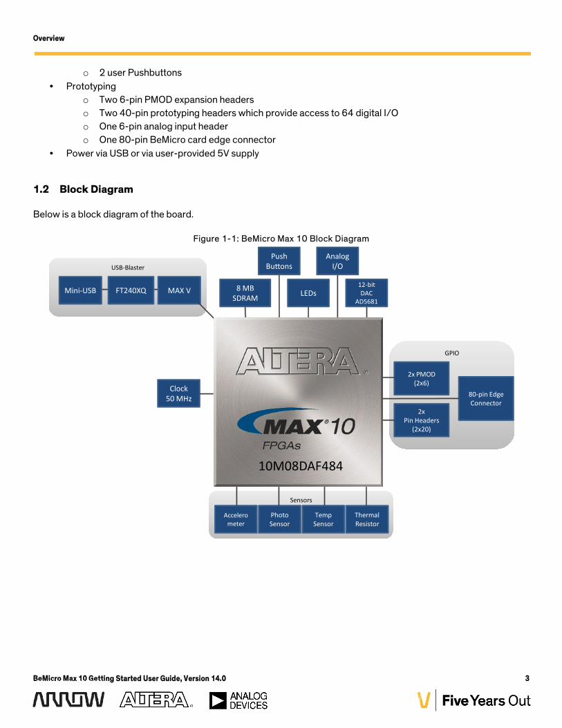
1.2 Block Diagram
Below is a block diagram of the board.
Figure 1-1: BeMicro Max 10 Block Diagram
Clock50 MHz
GPIO
2x PMOD(2x6)
2xPin Headers
(2x20)
80-pin EdgeConnector
Sensors
Accelerometer
PhotoSensor
TempSensor
ThermalResistor
8 MBSDRAM
USB-Blaster
Mini-USB MAX VFT240XQ
PushButtons
LEDs
AnalogI/O
12-bitDAC
AD5681
10M08DAF484
Overview
BeMicro Max 10 Getting Started User Guide, Version 14.0 3
o 2 user Pushbuttons Prototyping
o Two 6-pin PMOD expansion headerso Two 40-pin prototyping headers which provide access to 64 digital I/Oo One 6-pin analog input headero One 80-pin BeMicro card edge connector
Power via USB or via user-provided 5V supply
1.2 Block Diagram
Below is a block diagram of the board.
Figure 1-1: BeMicro Max 10 Block Diagram
Clock50 MHz
GPIO
2x PMOD(2x6)
2xPin Headers
(2x20)
80-pin EdgeConnector
Sensors
Accelerometer
PhotoSensor
TempSensor
ThermalResistor
8 MBSDRAM
USB-Blaster
Mini-USB MAX VFT240XQ
PushButtons
LEDs
AnalogI/O
12-bitDAC
AD5681
10M08DAF484
Overview
BeMicro Max 10 Getting Started User Guide, Version 14.0 4
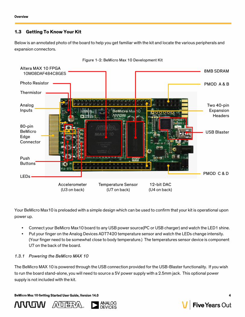
1.3 Getting To Know Your Kit
Below is an annotated photo of the board to help you get familiar with the kit and locate the various peripherals andexpansion connectors.
Figure 1-2: BeMicro Max 10 Development Kit
Altera MAX 10 FPGA10M08DAF484C8GES 8MB SDRAM
PushButtons
LEDs
Photo Resistor
Thermistor
80-pinBeMicroEdgeConnector
AnalogInputs
PMOD A & B
PMOD C & D
USB Blaster
Two 40-pinExpansion
Headers
Accelerometer(U3 on back)
Temperature Sensor(U7 on back)
12-bit DAC(U4 on back)
Your BeMicro Max10 is preloaded with a simple design which can be used to confirm that your kit is operational uponpower up.
Connect your BeMicro Max10 board to any USB power source(PC or USB charger) and watch the LED1 shine. Put your finger on the Analog Devices ADT7420 temperature sensor and watch the LEDs change intensity.
(Your finger need to be somewhat close to body temperature.) The temperatures sensor device is componentU7 on the back of the board.
1.3.1 Powering the BeMicro MAX 10
The BeMicro MAX 10 is powered through the USB connection provided for the USB-Blaster functionality. If you wishto run the board stand-alone, you will need to source a 5V power supply with a 2.5mm jack. This optional powersupply is not included with the kit.
Overview
BeMicro Max 10 Getting Started User Guide, Version 14.0 4
1.3 Getting To Know Your Kit
Below is an annotated photo of the board to help you get familiar with the kit and locate the various peripherals andexpansion connectors.
Figure 1-2: BeMicro Max 10 Development Kit
Altera MAX 10 FPGA10M08DAF484C8GES 8MB SDRAM
PushButtons
LEDs
Photo Resistor
Thermistor
80-pinBeMicroEdgeConnector
AnalogInputs
PMOD A & B
PMOD C & D
USB Blaster
Two 40-pinExpansion
Headers
Accelerometer(U3 on back)
Temperature Sensor(U7 on back)
12-bit DAC(U4 on back)
Your BeMicro Max10 is preloaded with a simple design which can be used to confirm that your kit is operational uponpower up.
Connect your BeMicro Max10 board to any USB power source(PC or USB charger) and watch the LED1 shine. Put your finger on the Analog Devices ADT7420 temperature sensor and watch the LEDs change intensity.
(Your finger need to be somewhat close to body temperature.) The temperatures sensor device is componentU7 on the back of the board.
1.3.1 Powering the BeMicro MAX 10
The BeMicro MAX 10 is powered through the USB connection provided for the USB-Blaster functionality. If you wishto run the board stand-alone, you will need to source a 5V power supply with a 2.5mm jack. This optional powersupply is not included with the kit.
Overview
BeMicro Max 10 Getting Started User Guide, Version 14.0 5
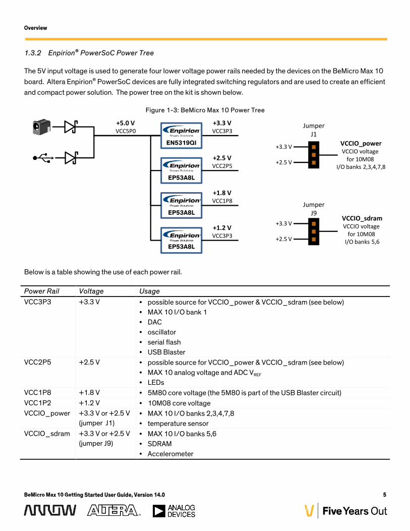
1.3.2 Enpirion® PowerSoC Power Tree
The 5V input voltage is used to generate four lower voltage power rails needed by the devices on the BeMicro Max 10board. Altera Enpirion® PowerSoC devices are fully integrated switching regulators and are used to create an efficientand compact power solution. The power tree on the kit is shown below.
Figure 1-3: BeMicro Max 10 Power Tree
EP53A8L
EP53A8L
EP53A8L
+5.0 VVCC5P0
+3.3 VVCC3P3
+2.5 VVCC2P5
+1.8 VVCC1P8
+1.2 VVCC3P3
JumperJ1
+3.3 V
+3.3 V
+2.5 V
+2.5 V
JumperJ9
VCCIO_powerVCCIO voltage
for 10M08I/O banks 2,3,4,7,8
VCCIO_sdramVCCIO voltage
for 10M08I/O banks 5,6
EN5319QI
Below is a table showing the use of each power rail.
Power Rail Voltage UsageVCC3P3 +3.3 V possible source for VCCIO_power & VCCIO_sdram (see below)
MAX 10 I/O bank 1 DAC oscillator serial flash USB Blaster
VCC2P5 +2.5 V possible source for VCCIO_power & VCCIO_sdram (see below) MAX 10 analog voltage and ADC VREF
LEDsVCC1P8 +1.8 V 5M80 core voltage (the 5M80 is part of the USB Blaster circuit)VCC1P2 +1.2 V 10M08 core voltageVCCIO_power +3.3 V or +2.5 V
(jumper J1) MAX 10 I/O banks 2,3,4,7,8 temperature sensor
VCCIO_sdram +3.3 V or +2.5 V(jumper J9)
MAX 10 I/O banks 5,6 SDRAM Accelerometer
Overview
BeMicro Max 10 Getting Started User Guide, Version 14.0 5
1.3.2 Enpirion® PowerSoC Power Tree
The 5V input voltage is used to generate four lower voltage power rails needed by the devices on the BeMicro Max 10board. Altera Enpirion® PowerSoC devices are fully integrated switching regulators and are used to create an efficientand compact power solution. The power tree on the kit is shown below.
Figure 1-3: BeMicro Max 10 Power Tree
EP53A8L
EP53A8L
EP53A8L
+5.0 VVCC5P0
+3.3 VVCC3P3
+2.5 VVCC2P5
+1.8 VVCC1P8
+1.2 VVCC3P3
JumperJ1
+3.3 V
+3.3 V
+2.5 V
+2.5 V
JumperJ9
VCCIO_powerVCCIO voltage
for 10M08I/O banks 2,3,4,7,8
VCCIO_sdramVCCIO voltage
for 10M08I/O banks 5,6
EN5319QI
Below is a table showing the use of each power rail.
Power Rail Voltage UsageVCC3P3 +3.3 V possible source for VCCIO_power & VCCIO_sdram (see below)
MAX 10 I/O bank 1 DAC oscillator serial flash USB Blaster
VCC2P5 +2.5 V possible source for VCCIO_power & VCCIO_sdram (see below) MAX 10 analog voltage and ADC VREF
LEDsVCC1P8 +1.8 V 5M80 core voltage (the 5M80 is part of the USB Blaster circuit)VCC1P2 +1.2 V 10M08 core voltageVCCIO_power +3.3 V or +2.5 V
(jumper J1) MAX 10 I/O banks 2,3,4,7,8 temperature sensor
VCCIO_sdram +3.3 V or +2.5 V(jumper J9)
MAX 10 I/O banks 5,6 SDRAM Accelerometer
Software Installation
BeMicro Max 10 Getting Started User Guide, Version 14.0 6
2. SOFTWARE INSTALLATION
This section lists the required software design tools and explains how to install the software needed to create andcompile designs for your MAX 10 FPGA.
List of Required Software:
Altera Quartus II v14.0 with Update 2 (or newer) BeMicro Max 10 Evaluation Kit Files USB-Blaster™ Driver
2.1 Install the Altera Design Software
The MAX 10 FPGA device family is supported in Quartus II software versions 14.0.2 and newer. You will need todownload and install the following design software package:
Quartus II Web Edition design software v14.0 – FPGA synthesis and compilation tool that includesthe IP Catalog and QSys integration tools. You will first install the full installation of version 14.0. Thisinstallation will not contain support for MAX 10 FPGA so it will need to be updated to 14.0.2 or newer.Web Edition is a free version of the software with no licensing required.NOTE: Subscription Edition, which requires a paid license, can be used in place of Web Edition.
Quartus II Software v14.0 Update 2 – This is an update to Quartus which will add support for MAX10 FPGA.
2.1.1 Download and Install Quartus II Web Edition v14.0
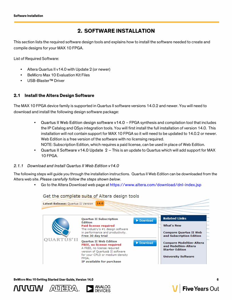
The following steps will guide you through the installation instructions. Quartus II Web Edition can be downloaded from theAltera web site. Please carefully follow the steps shown below.
Go to the Altera Download web page at https://www.altera.com/download/dnl-index.jsp
Software Installation
BeMicro Max 10 Getting Started User Guide, Version 14.0 6
2. SOFTWARE INSTALLATION
This section lists the required software design tools and explains how to install the software needed to create andcompile designs for your MAX 10 FPGA.
List of Required Software:
Altera Quartus II v14.0 with Update 2 (or newer) BeMicro Max 10 Evaluation Kit Files USB-Blaster™ Driver
2.1 Install the Altera Design Software
The MAX 10 FPGA device family is supported in Quartus II software versions 14.0.2 and newer. You will need todownload and install the following design software package:
Quartus II Web Edition design software v14.0 – FPGA synthesis and compilation tool that includesthe IP Catalog and QSys integration tools. You will first install the full installation of version 14.0. Thisinstallation will not contain support for MAX 10 FPGA so it will need to be updated to 14.0.2 or newer.Web Edition is a free version of the software with no licensing required.NOTE: Subscription Edition, which requires a paid license, can be used in place of Web Edition.
Quartus II Software v14.0 Update 2 – This is an update to Quartus which will add support for MAX10 FPGA.
2.1.1 Download and Install Quartus II Web Edition v14.0
The following steps will guide you through the installation instructions. Quartus II Web Edition can be downloaded from theAltera web site. Please carefully follow the steps shown below.
Go to the Altera Download web page at https://www.altera.com/download/dnl-index.jsp
Software Installation
BeMicro Max 10 Getting Started User Guide, Version 14.0 7
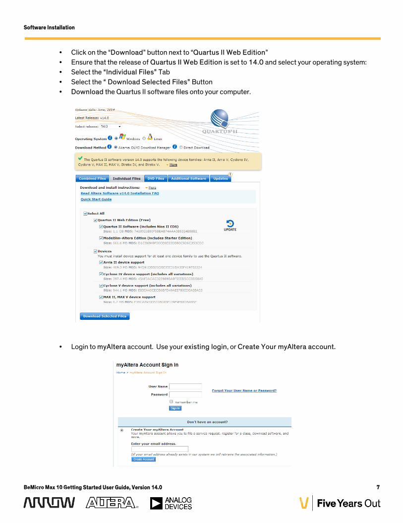
Click on the “Download” button next to “Quartus II Web Edition” Ensure that the release of Quartus II Web Edition is set to 14.0 and select your operating system: Select the “Individual Files” Tab Select the “ Download Selected Files” Button Download the Quartus II software files onto your computer.
Login to myAltera account. Use your existing login, or Create Your myAltera account.
Software Installation
BeMicro Max 10 Getting Started User Guide, Version 14.0 7
Click on the “Download” button next to “Quartus II Web Edition” Ensure that the release of Quartus II Web Edition is set to 14.0 and select your operating system: Select the “Individual Files” Tab Select the “ Download Selected Files” Button Download the Quartus II software files onto your computer.
Login to myAltera account. Use your existing login, or Create Your myAltera account.
Software Installation
BeMicro Max 10 Getting Started User Guide, Version 14.0 8
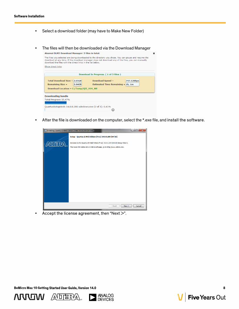
Select a download folder (may have to Make New Folder)
The files will then be downloaded via the Download Manager
After the file is downloaded on the computer, select the *.exe file, and install the software.
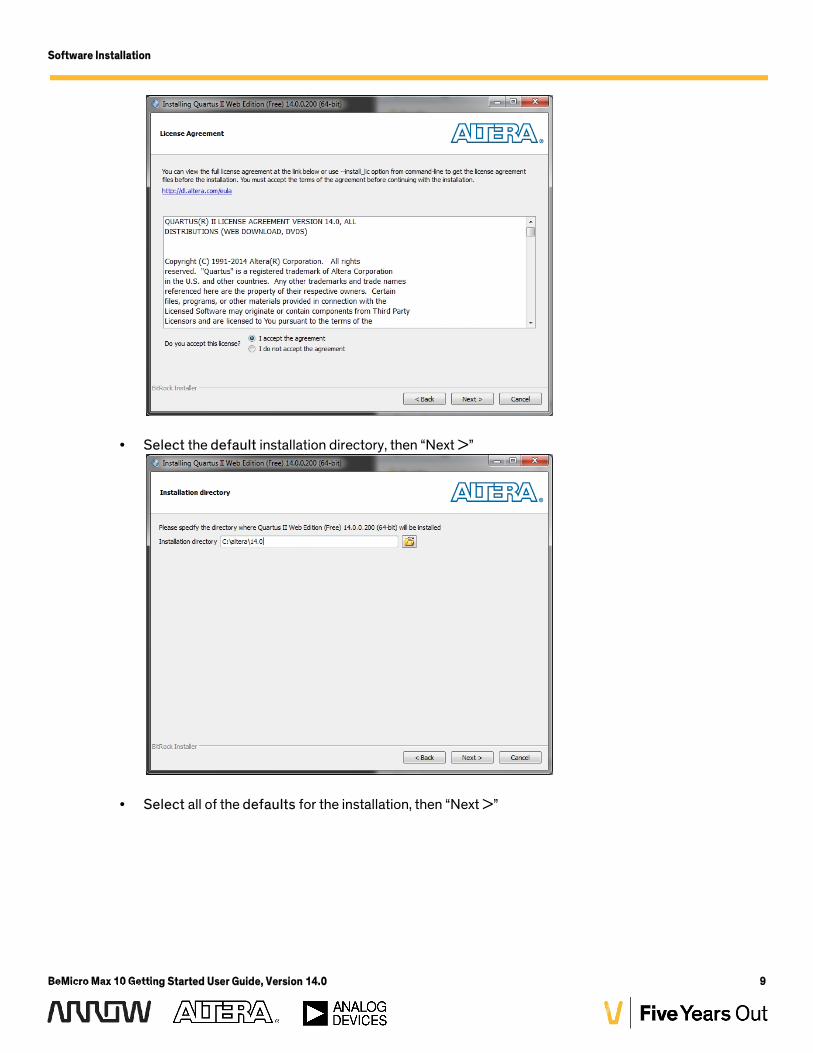
Accept the license agreement, then “Next >”.
Software Installation
BeMicro Max 10 Getting Started User Guide, Version 14.0 8
Select a download folder (may have to Make New Folder)
The files will then be downloaded via the Download Manager
After the file is downloaded on the computer, select the *.exe file, and install the software.
Accept the license agreement, then “Next >”.
Software Installation
BeMicro Max 10 Getting Started User Guide, Version 14.0 9
Select the default installation directory, then “Next >”
Select all of the defaults for the installation, then “Next >”
Software Installation
BeMicro Max 10 Getting Started User Guide, Version 14.0 9
Select the default installation directory, then “Next >”
Select all of the defaults for the installation, then “Next >”
Software Installation
BeMicro Max 10 Getting Started User Guide, Version 14.0 9
Select the default installation directory, then “Next >”
Select all of the defaults for the installation, then “Next >”
Software Installation
BeMicro Max 10 Getting Started User Guide, Version 14.0 10
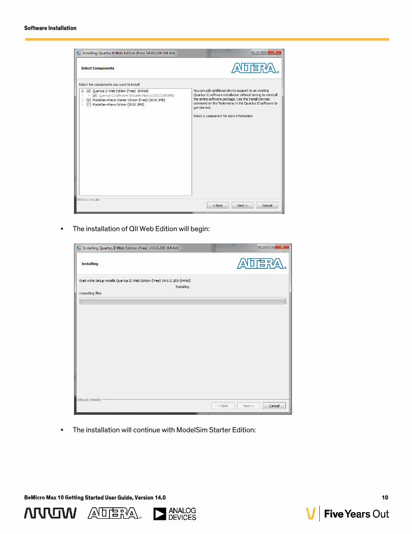
The installation of QII Web Edition will begin:
The installation will continue with ModelSim Starter Edition:
Software Installation
BeMicro Max 10 Getting Started User Guide, Version 14.0 10
The installation of QII Web Edition will begin:
The installation will continue with ModelSim Starter Edition:
Software Installation
BeMicro Max 10 Getting Started User Guide, Version 14.0 10
The installation of QII Web Edition will begin:
The installation will continue with ModelSim Starter Edition:
Software Installation
BeMicro Max 10 Getting Started User Guide, Version 14.0 11
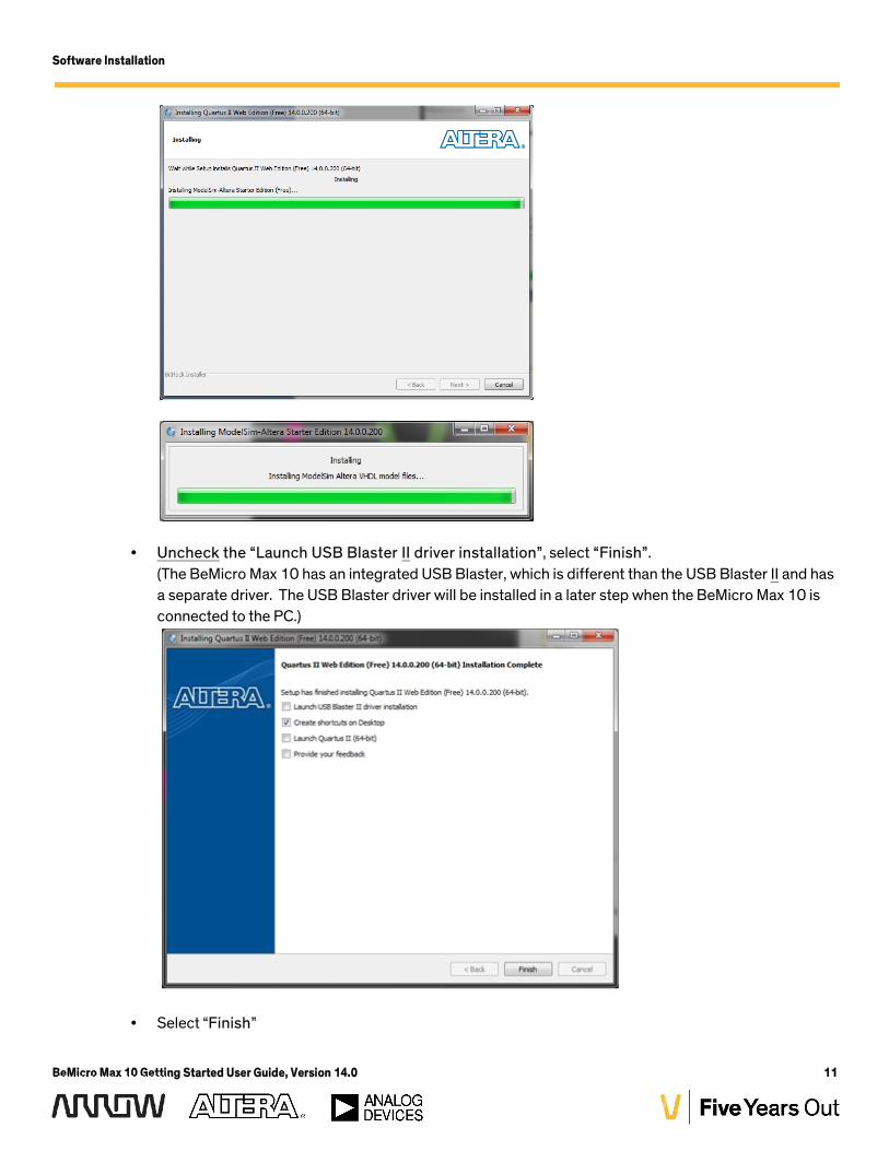
Uncheck the “Launch USB Blaster II driver installation”, select “Finish”.(The BeMicro Max 10 has an integrated USB Blaster, which is different than the USB Blaster II and hasa separate driver. The USB Blaster driver will be installed in a later step when the BeMicro Max 10 isconnected to the PC.)
Select “Finish”
Software Installation
BeMicro Max 10 Getting Started User Guide, Version 14.0 11
Uncheck the “Launch USB Blaster II driver installation”, select “Finish”.(The BeMicro Max 10 has an integrated USB Blaster, which is different than the USB Blaster II and hasa separate driver. The USB Blaster driver will be installed in a later step when the BeMicro Max 10 isconnected to the PC.)
Select “Finish”
Software Installation
BeMicro Max 10 Getting Started User Guide, Version 14.0 12
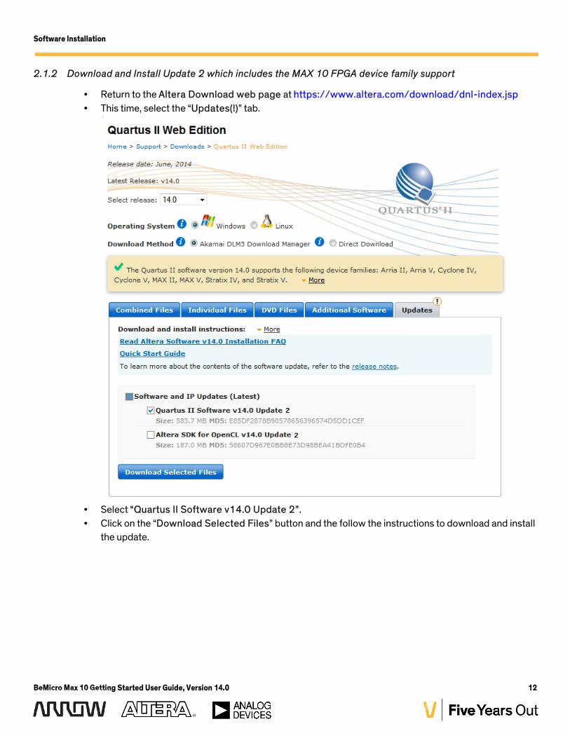
2.1.2 Download and Install Update 2 which includes the MAX 10 FPGA device family support
Return to the Altera Download web page at https://www.altera.com/download/dnl-index.jsp This time, select the “Updates(!)” tab.
Select “Quartus II Software v14.0 Update 2”. Click on the “Download Selected Files” button and the follow the instructions to download and install
the update.
Software Installation
BeMicro Max 10 Getting Started User Guide, Version 14.0 12
2.1.2 Download and Install Update 2 which includes the MAX 10 FPGA device family support
Return to the Altera Download web page at https://www.altera.com/download/dnl-index.jsp This time, select the “Updates(!)” tab.
Select “Quartus II Software v14.0 Update 2”. Click on the “Download Selected Files” button and the follow the instructions to download and install
the update.
Software Installation
BeMicro Max 10 Getting Started User Guide, Version 14.0 13
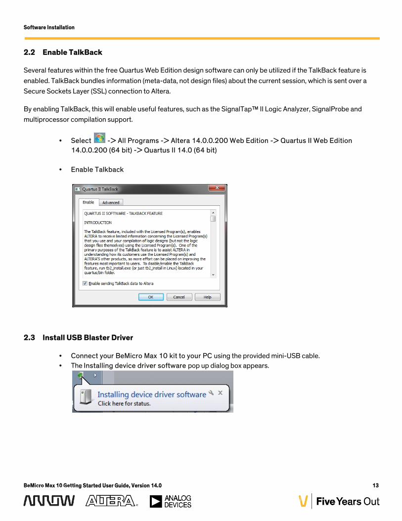
2.2 Enable TalkBack
Several features within the free Quartus Web Edition design software can only be utilized if the TalkBack feature isenabled. TalkBack bundles information (meta-data, not design files) about the current session, which is sent over aSecure Sockets Layer (SSL) connection to Altera.
By enabling TalkBack, this will enable useful features, such as the SignalTap™ II Logic Analyzer, SignalProbe andmultiprocessor compilation support.
Select -> All Programs -> Altera 14.0.0.200 Web Edition -> Quartus II Web Edition14.0.0.200 (64 bit) -> Quartus II 14.0 (64 bit)
Enable Talkback
2.3 Install USB Blaster Driver
Connect your BeMicro Max 10 kit to your PC using the provided mini-USB cable. The Installing device driver software pop up dialog box appears.
Software Installation
BeMicro Max 10 Getting Started User Guide, Version 14.0 13
2.2 Enable TalkBack
Several features within the free Quartus Web Edition design software can only be utilized if the TalkBack feature isenabled. TalkBack bundles information (meta-data, not design files) about the current session, which is sent over aSecure Sockets Layer (SSL) connection to Altera.
By enabling TalkBack, this will enable useful features, such as the SignalTap™ II Logic Analyzer, SignalProbe andmultiprocessor compilation support.
Select -> All Programs -> Altera 14.0.0.200 Web Edition -> Quartus II Web Edition14.0.0.200 (64 bit) -> Quartus II 14.0 (64 bit)
Enable Talkback
2.3 Install USB Blaster Driver
Connect your BeMicro Max 10 kit to your PC using the provided mini-USB cable. The Installing device driver software pop up dialog box appears.
Software Installation
BeMicro Max 10 Getting Started User Guide, Version 14.0 14
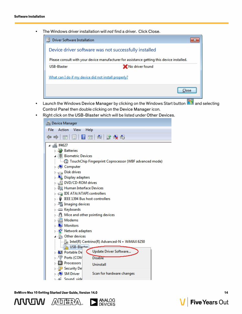
The Windows driver installation will not find a driver. Click Close.
Launch the Windows Device Manager by clicking on the Windows Start button and selectingControl Panel then double clicking on the Device Manager icon.
Right click on the USB-Blaster which will be listed under Other Devices.
Software Installation
BeMicro Max 10 Getting Started User Guide, Version 14.0 14
The Windows driver installation will not find a driver. Click Close.
Launch the Windows Device Manager by clicking on the Windows Start button and selectingControl Panel then double clicking on the Device Manager icon.
Right click on the USB-Blaster which will be listed under Other Devices.
Software Installation
BeMicro Max 10 Getting Started User Guide, Version 14.0 15
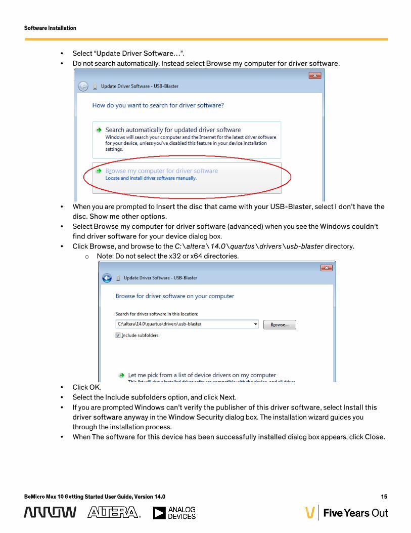
Select “Update Driver Software…”. Do not search automatically. Instead select Browse my computer for driver software.
When you are prompted to Insert the disc that came with your USB-Blaster, select I don’t have thedisc. Show me other options.
Select Browse my computer for driver software (advanced) when you see the Windows couldn’tfind driver software for your device dialog box.
Click Browse, and browse to the C:\altera\14.0\quartus\drivers\usb-blaster directory.o Note: Do not select the x32 or x64 directories.
Click OK. Select the Include subfolders option, and click Next. If you are prompted Windows can’t verify the publisher of this driver software, select Install this
driver software anyway in the Window Security dialog box. The installation wizard guides youthrough the installation process.
When The software for this device has been successfully installed dialog box appears, click Close.
Software Installation
BeMicro Max 10 Getting Started User Guide, Version 14.0 15
Select “Update Driver Software…”. Do not search automatically. Instead select Browse my computer for driver software.
When you are prompted to Insert the disc that came with your USB-Blaster, select I don’t have thedisc. Show me other options.
Select Browse my computer for driver software (advanced) when you see the Windows couldn’tfind driver software for your device dialog box.
Click Browse, and browse to the C:\altera\14.0\quartus\drivers\usb-blaster directory.o Note: Do not select the x32 or x64 directories.
Click OK. Select the Include subfolders option, and click Next. If you are prompted Windows can’t verify the publisher of this driver software, select Install this
driver software anyway in the Window Security dialog box. The installation wizard guides youthrough the installation process.
When The software for this device has been successfully installed dialog box appears, click Close.
Software Installation
BeMicro Max 10 Getting Started User Guide, Version 14.0 16
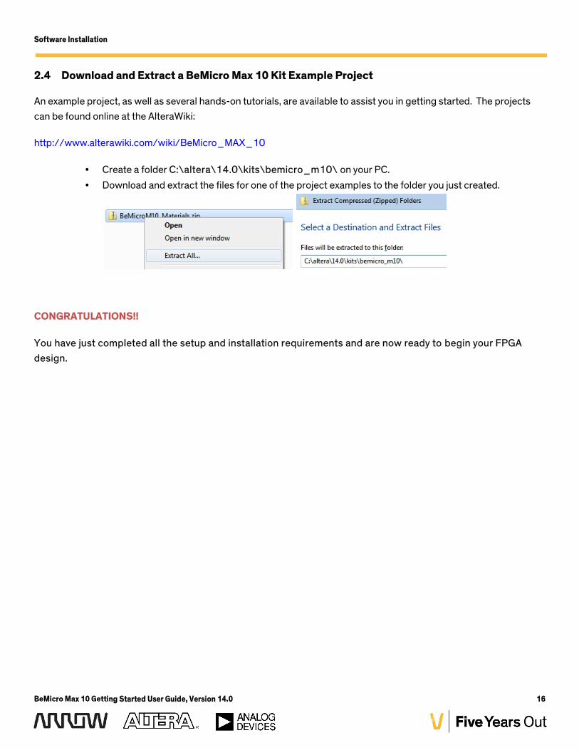
2.4 Download and Extract a BeMicro Max 10 Kit Example Project
An example project, as well as several hands-on tutorials, are available to assist you in getting started. The projectscan be found online at the AlteraWiki:
http://www.alterawiki.com/wiki/BeMicro_MAX_10
Create a folder C:\altera\14.0\kits\bemicro_m10\ on your PC. Download and extract the files for one of the project examples to the folder you just created.
CONGRATULATIONS!!
You have just completed all the setup and installation requirements and are now ready to begin your FPGAdesign.
Software Installation
BeMicro Max 10 Getting Started User Guide, Version 14.0 16
2.4 Download and Extract a BeMicro Max 10 Kit Example Project
An example project, as well as several hands-on tutorials, are available to assist you in getting started. The projectscan be found online at the AlteraWiki:
http://www.alterawiki.com/wiki/BeMicro_MAX_10
Create a folder C:\altera\14.0\kits\bemicro_m10\ on your PC. Download and extract the files for one of the project examples to the folder you just created.
CONGRATULATIONS!!
You have just completed all the setup and installation requirements and are now ready to begin your FPGAdesign.
Pinout Information for MAX 10 FPGA I/O
BeMicro Max 10 Getting Started User Guide, Version 14.0 17
3. PINOUT INFORMATION FOR MAX 10 FPGA I/O
The BeMicro Max 10 contains a variety of external peripheral devices and expansion headers connected to the MAX10 FPGA’s configurable I/O pins. The details of the board circuitry and these connections can be found in theschematic for the kit. (Refer to Section 2.4 for details on locating these files.)
This section presents the information in the schematic organized into pinout tables by peripheral. While the schematicprovides a board level view of all the pins for a given connector or peripheral, the tables in this section focus on theFPGA signals needed for FPGA pin assignment and compilation. The “Signal Name” column in the tables throughoutthis section indicates the naming of the signal in the Quartus projects’ QSF1 file provided in the various FPGA projects.
3.1 Analog Devices External Peripherals
3.1.1 Accelerometer, 3-Axis, SPI interface (ADXL362)
Signal Name MAX 10 PinADXL362_CS L14ADXL362_INT1 M15ADXL362_INT2 M14ADXL362_MISO L18ADXL362_MOSI L19ADXL362_SCLK M18
3.1.2 DAC, 12-bit, SPI interface (AD5681)
Signal Name MAX 10 PinAD5681R_LDACn N18AD5681R_RSTn L15AD5681R_SCL G17AD5681R_SDA H17AD5681R_SYNCn N19
3.1.3 Temperature sensor, I2C interface (ADT7420)
Signal Name MAX 10 PinADT7420_CT P13ADT7420_INT AB14ADT7420_SCL W13ADT7420_SDA R13
1 A “QSF file” is a Quartus Settings File, a file with extension of *.qsf, in which Quartus stores all project settings including pin assignments.
Pinout Information for MAX 10 FPGA I/O
BeMicro Max 10 Getting Started User Guide, Version 14.0 18
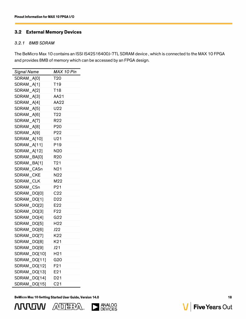
3.2 External Memory Devices
3.2.1 8MB SDRAM
The BeMicro Max 10 contains an ISSI IS42S16400J-7TL SDRAM device , which is connected to the MAX 10 FPGAand provides 8MB of memory which can be accessed by an FPGA design.
Signal Name MAX 10 PinSDRAM_A[0] T20SDRAM_A[1] T19SDRAM_A[2] T18SDRAM_A[3] AA21SDRAM_A[4] AA22SDRAM_A[5] U22SDRAM_A[6] T22SDRAM_A[7] R22SDRAM_A[8] P20SDRAM_A[9] P22SDRAM_A[10] U21SDRAM_A[11] P19SDRAM_A[12] N20SDRAM_BA[0] R20SDRAM_BA[1] T21SDRAM_CASn N21SDRAM_CKE N22SDRAM_CLK M22SDRAM_CSn P21SDRAM_DQ[0] C22SDRAM_DQ[1] D22SDRAM_DQ[2] E22SDRAM_DQ[3] F22SDRAM_DQ[4] G22SDRAM_DQ[5] H22SDRAM_DQ[6] J22SDRAM_DQ[7] K22SDRAM_DQ[8] K21SDRAM_DQ[9] J21SDRAM_DQ[10] H21SDRAM_DQ[11] G20SDRAM_DQ[12] F21SDRAM_DQ[13] E21SDRAM_DQ[14] D21SDRAM_DQ[15] C21
Pinout Information for MAX 10 FPGA I/O
BeMicro Max 10 Getting Started User Guide, Version 14.0 18
3.2 External Memory Devices
3.2.1 8MB SDRAM
The BeMicro Max 10 contains an ISSI IS42S16400J-7TL SDRAM device , which is connected to the MAX 10 FPGAand provides 8MB of memory which can be accessed by an FPGA design.
Signal Name MAX 10 PinSDRAM_A[0] T20SDRAM_A[1] T19SDRAM_A[2] T18SDRAM_A[3] AA21SDRAM_A[4] AA22SDRAM_A[5] U22SDRAM_A[6] T22SDRAM_A[7] R22SDRAM_A[8] P20SDRAM_A[9] P22SDRAM_A[10] U21SDRAM_A[11] P19SDRAM_A[12] N20SDRAM_BA[0] R20SDRAM_BA[1] T21SDRAM_CASn N21SDRAM_CKE N22SDRAM_CLK M22SDRAM_CSn P21SDRAM_DQ[0] C22SDRAM_DQ[1] D22SDRAM_DQ[2] E22SDRAM_DQ[3] F22SDRAM_DQ[4] G22SDRAM_DQ[5] H22SDRAM_DQ[6] J22SDRAM_DQ[7] K22SDRAM_DQ[8] K21SDRAM_DQ[9] J21SDRAM_DQ[10] H21SDRAM_DQ[11] G20SDRAM_DQ[12] F21SDRAM_DQ[13] E21SDRAM_DQ[14] D21SDRAM_DQ[15] C21
Pinout Information for MAX 10 FPGA I/O
BeMicro Max 10 Getting Started User Guide, Version 14.0 19
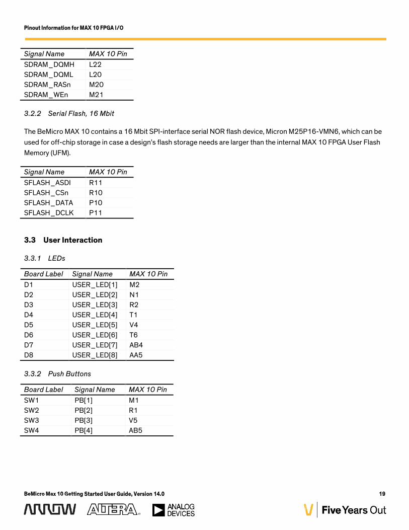
Signal Name MAX 10 PinSDRAM_DQMH L22SDRAM_DQML L20SDRAM_RASn M20SDRAM_WEn M21
3.2.2 Serial Flash, 16 Mbit
The BeMicro MAX 10 contains a 16 Mbit SPI-interface serial NOR flash device, Micron M25P16-VMN6, which can beused for off-chip storage in case a design’s flash storage needs are larger than the internal MAX 10 FPGA User FlashMemory (UFM).
Signal Name MAX 10 PinSFLASH_ASDI R11SFLASH_CSn R10SFLASH_DATA P10SFLASH_DCLK P11
3.3 User Interaction
3.3.1 LEDs
Board Label Signal Name MAX 10 PinD1 USER_LED[1] M2D2 USER_LED[2] N1D3 USER_LED[3] R2D4 USER_LED[4] T1D5 USER_LED[5] V4D6 USER_LED[6] T6D7 USER_LED[7] AB4D8 USER_LED[8] AA5
3.3.2 Push Buttons
Board Label Signal Name MAX 10 PinSW1 PB[1] M1SW2 PB[2] R1SW3 PB[3] V5SW4 PB[4] AB5
Pinout Information for MAX 10 FPGA I/O
BeMicro Max 10 Getting Started User Guide, Version 14.0 19
Signal Name MAX 10 PinSDRAM_DQMH L22SDRAM_DQML L20SDRAM_RASn M20SDRAM_WEn M21
3.2.2 Serial Flash, 16 Mbit
The BeMicro MAX 10 contains a 16 Mbit SPI-interface serial NOR flash device, Micron M25P16-VMN6, which can beused for off-chip storage in case a design’s flash storage needs are larger than the internal MAX 10 FPGA User FlashMemory (UFM).
Signal Name MAX 10 PinSFLASH_ASDI R11SFLASH_CSn R10SFLASH_DATA P10SFLASH_DCLK P11
3.3 User Interaction
3.3.1 LEDs
Board Label Signal Name MAX 10 PinD1 USER_LED[1] M2D2 USER_LED[2] N1D3 USER_LED[3] R2D4 USER_LED[4] T1D5 USER_LED[5] V4D6 USER_LED[6] T6D7 USER_LED[7] AB4D8 USER_LED[8] AA5
3.3.2 Push Buttons
Board Label Signal Name MAX 10 PinSW1 PB[1] M1SW2 PB[2] R1SW3 PB[3] V5SW4 PB[4] AB5
Pinout Information for MAX 10 FPGA I/O
BeMicro Max 10 Getting Started User Guide, Version 14.0 20
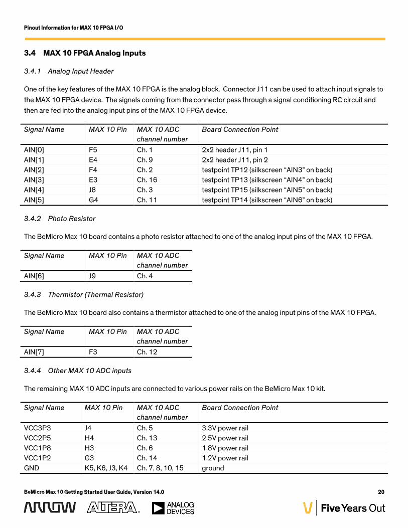
3.4 MAX 10 FPGA Analog Inputs
3.4.1 Analog Input Header
One of the key features of the MAX 10 FPGA is the analog block. Connector J11 can be used to attach input signals tothe MAX 10 FPGA device. The signals coming from the connector pass through a signal conditioning RC circuit andthen are fed into the analog input pins of the MAX 10 FPGA device.
Signal Name MAX 10 Pin MAX 10 ADCchannel number
Board Connection Point
AIN[0] F5 Ch. 1 2x2 header J11, pin 1AIN[1] E4 Ch. 9 2x2 header J11, pin 2AIN[2] F4 Ch. 2 testpoint TP12 (silkscreen “AIN3” on back)AIN[3] E3 Ch. 16 testpoint TP13 (silkscreen “AIN4” on back)AIN[4] J8 Ch. 3 testpoint TP15 (silkscreen “AIN5” on back)AIN[5] G4 Ch. 11 testpoint TP14 (silkscreen “AIN6” on back)
3.4.2 Photo Resistor
The BeMicro Max 10 board contains a photo resistor attached to one of the analog input pins of the MAX 10 FPGA.
Signal Name MAX 10 Pin MAX 10 ADCchannel number
AIN[6] J9 Ch. 4
3.4.3 Thermistor (Thermal Resistor)
The BeMicro Max 10 board also contains a thermistor attached to one of the analog input pins of the MAX 10 FPGA.
Signal Name MAX 10 Pin MAX 10 ADCchannel number
AIN[7] F3 Ch. 12
3.4.4 Other MAX 10 ADC inputs
The remaining MAX 10 ADC inputs are connected to various power rails on the BeMicro Max 10 kit.
Signal Name MAX 10 Pin MAX 10 ADCchannel number
Board Connection Point
VCC3P3 J4 Ch. 5 3.3V power railVCC2P5 H4 Ch. 13 2.5V power railVCC1P8 H3 Ch. 6 1.8V power railVCC1P2 G3 Ch. 14 1.2V power railGND K5, K6, J3, K4 Ch. 7, 8, 10, 15 ground
Pinout Information for MAX 10 FPGA I/O
BeMicro Max 10 Getting Started User Guide, Version 14.0 20
3.4 MAX 10 FPGA Analog Inputs
3.4.1 Analog Input Header
One of the key features of the MAX 10 FPGA is the analog block. Connector J11 can be used to attach input signals tothe MAX 10 FPGA device. The signals coming from the connector pass through a signal conditioning RC circuit andthen are fed into the analog input pins of the MAX 10 FPGA device.
Signal Name MAX 10 Pin MAX 10 ADCchannel number
Board Connection Point
AIN[0] F5 Ch. 1 2x2 header J11, pin 1AIN[1] E4 Ch. 9 2x2 header J11, pin 2AIN[2] F4 Ch. 2 testpoint TP12 (silkscreen “AIN3” on back)AIN[3] E3 Ch. 16 testpoint TP13 (silkscreen “AIN4” on back)AIN[4] J8 Ch. 3 testpoint TP15 (silkscreen “AIN5” on back)AIN[5] G4 Ch. 11 testpoint TP14 (silkscreen “AIN6” on back)
3.4.2 Photo Resistor
The BeMicro Max 10 board contains a photo resistor attached to one of the analog input pins of the MAX 10 FPGA.
Signal Name MAX 10 Pin MAX 10 ADCchannel number
AIN[6] J9 Ch. 4
3.4.3 Thermistor (Thermal Resistor)
The BeMicro Max 10 board also contains a thermistor attached to one of the analog input pins of the MAX 10 FPGA.
Signal Name MAX 10 Pin MAX 10 ADCchannel number
AIN[7] F3 Ch. 12
3.4.4 Other MAX 10 ADC inputs
The remaining MAX 10 ADC inputs are connected to various power rails on the BeMicro Max 10 kit.
Signal Name MAX 10 Pin MAX 10 ADCchannel number
Board Connection Point
VCC3P3 J4 Ch. 5 3.3V power railVCC2P5 H4 Ch. 13 2.5V power railVCC1P8 H3 Ch. 6 1.8V power railVCC1P2 G3 Ch. 14 1.2V power railGND K5, K6, J3, K4 Ch. 7, 8, 10, 15 ground
Pinout Information for MAX 10 FPGA I/O
BeMicro Max 10 Getting Started User Guide, Version 14.0 21
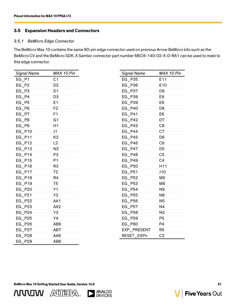
3.5 Expansion Headers and Connectors
3.5.1 BeMicro Edge Connector
The BeMicro Max 10 contains the same 80-pin edge connector used on previous Arrow BeMicro kits such as theBeMicro CV and the BeMicro SDK. A Samtec connector part number MEC6-140-02-X-D-RA1 can be used to mate tothis edge connector.
Signal Name MAX 10 PinEG_P1 C1EG_P2 D2EG_P3 D1EG_P4 D3EG_P5 E1EG_P6 F2EG_P7 F1EG_P8 G1EG_P9 H1EG_P10 J1EG_P11 K2EG_P12 L2EG_P13 N2EG_P14 P3EG_P15 P1EG_P16 R3EG_P17 T2EG_P18 R4EG_P19 T5EG_P20 Y1EG_P21 Y2EG_P22 AA1EG_P23 AA2EG_P24 Y3EG_P25 Y4EG_P26 AB6EG_P27 AB7EG_P28 AA8EG_P29 AB8
Signal Name MAX 10 PinEG_P35 E11EG_P36 E10EG_P37 D9EG_P38 E9EG_P39 E8EG_P40 D8EG_P41 E6EG_P42 D7EG_P43 C8EG_P44 C7EG_P45 D6EG_P46 C6EG_P47 D5EG_P48 C5EG_P49 C4EG_P50 H11EG_P51 J10EG_P52 M9EG_P53 M8EG_P54 N9EG_P55 N8EG_P56 N5EG_P57 N4EG_P58 N3EG_P59 P5EG_P60 P4EXP_PRESENT R5RESET_EXPn C2
Pinout Information for MAX 10 FPGA I/O
BeMicro Max 10 Getting Started User Guide, Version 14.0 21
3.5 Expansion Headers and Connectors
3.5.1 BeMicro Edge Connector
The BeMicro Max 10 contains the same 80-pin edge connector used on previous Arrow BeMicro kits such as theBeMicro CV and the BeMicro SDK. A Samtec connector part number MEC6-140-02-X-D-RA1 can be used to mate tothis edge connector.
Signal Name MAX 10 PinEG_P1 C1EG_P2 D2EG_P3 D1EG_P4 D3EG_P5 E1EG_P6 F2EG_P7 F1EG_P8 G1EG_P9 H1EG_P10 J1EG_P11 K2EG_P12 L2EG_P13 N2EG_P14 P3EG_P15 P1EG_P16 R3EG_P17 T2EG_P18 R4EG_P19 T5EG_P20 Y1EG_P21 Y2EG_P22 AA1EG_P23 AA2EG_P24 Y3EG_P25 Y4EG_P26 AB6EG_P27 AB7EG_P28 AA8EG_P29 AB8
Signal Name MAX 10 PinEG_P35 E11EG_P36 E10EG_P37 D9EG_P38 E9EG_P39 E8EG_P40 D8EG_P41 E6EG_P42 D7EG_P43 C8EG_P44 C7EG_P45 D6EG_P46 C6EG_P47 D5EG_P48 C5EG_P49 C4EG_P50 H11EG_P51 J10EG_P52 M9EG_P53 M8EG_P54 N9EG_P55 N8EG_P56 N5EG_P57 N4EG_P58 N3EG_P59 P5EG_P60 P4EXP_PRESENT R5RESET_EXPn C2
Pinout Information for MAX 10 FPGA I/O
BeMicro Max 10 Getting Started User Guide, Version 14.0 22
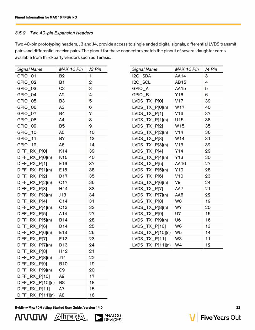
3.5.2 Two 40-pin Expansion Headers
Two 40-pin prototyping headers, J3 and J4, provide access to single ended digital signals, differential LVDS transmitpairs and differential receive pairs. The pinout for these connectors match the pinout of several daughter cardsavailable from third-party vendors such as Terasic.
Signal Name MAX 10 Pin J3 PinGPIO_01 B2 1GPIO_02 B1 2GPIO_03 C3 3GPIO_04 A2 4GPIO_05 B3 5GPIO_06 A3 6GPIO_07 B4 7GPIO_08 A4 8GPIO_09 B5 9GPIO_10 A5 10GPIO_11 B7 13GPIO_12 A6 14DIFF_RX_P[0] K14 39DIFF_RX_P[0](n) K15 40DIFF_RX_P[1] E16 37DIFF_RX_P[1](n) E15 38DIFF_RX_P[2] D17 35DIFF_RX_P[2](n) C17 36DIFF_RX_P[3] H14 33DIFF_RX_P[3](n) J13 34DIFF_RX_P[4] C14 31DIFF_RX_P[4](n) C13 32DIFF_RX_P[5] A14 27DIFF_RX_P[5](n) B14 28DIFF_RX_P[6] D14 25DIFF_RX_P[6](n) E13 26DIFF_RX_P[7] E12 23DIFF_RX_P[7](n) D13 24DIFF_RX_P[8] H12 21DIFF_RX_P[8](n) J11 22DIFF_RX_P[9] B10 19DIFF_RX_P[9](n) C9 20DIFF_RX_P[10] A9 17DIFF_RX_P[10](n) B8 18DIFF_RX_P[11] A7 15DIFF_RX_P[11](n) A8 16
Signal Name MAX 10 Pin J4 PinI2C_SDA AA14 3I2C_SCL AB15 4GPIO_A AA15 5GPIO_B Y16 6LVDS_TX_P[0] V17 39LVDS_TX_P[0](n) W17 40LVDS_TX_P[1] V16 37LVDS_TX_P[1](n) U15 38LVDS_TX_P[2] W15 35LVDS_TX_P[2](n) V14 36LVDS_TX_P[3] W14 31LVDS_TX_P[3](n) V13 32LVDS_TX_P[4] Y14 29LVDS_TX_P[4](n) Y13 30LVDS_TX_P[5] AA10 27LVDS_TX_P[5](n) Y10 28LVDS_TX_P[6] V10 23LVDS_TX_P[6](n) V9 24LVDS_TX_P[7] AA7 21LVDS_TX_P[7](n) AA6 22LVDS_TX_P[8] W8 19LVDS_TX_P[8](n) W7 20LVDS_TX_P[9] U7 15LVDS_TX_P[9](n) U6 16LVDS_TX_P[10] W6 13LVDS_TX_P[10](n) W5 14LVDS_TX_P[11] W3 11LVDS_TX_P[11](n) W4 12
Pinout Information for MAX 10 FPGA I/O
BeMicro Max 10 Getting Started User Guide, Version 14.0 22
3.5.2 Two 40-pin Expansion Headers
Two 40-pin prototyping headers, J3 and J4, provide access to single ended digital signals, differential LVDS transmitpairs and differential receive pairs. The pinout for these connectors match the pinout of several daughter cardsavailable from third-party vendors such as Terasic.
Signal Name MAX 10 Pin J3 PinGPIO_01 B2 1GPIO_02 B1 2GPIO_03 C3 3GPIO_04 A2 4GPIO_05 B3 5GPIO_06 A3 6GPIO_07 B4 7GPIO_08 A4 8GPIO_09 B5 9GPIO_10 A5 10GPIO_11 B7 13GPIO_12 A6 14DIFF_RX_P[0] K14 39DIFF_RX_P[0](n) K15 40DIFF_RX_P[1] E16 37DIFF_RX_P[1](n) E15 38DIFF_RX_P[2] D17 35DIFF_RX_P[2](n) C17 36DIFF_RX_P[3] H14 33DIFF_RX_P[3](n) J13 34DIFF_RX_P[4] C14 31DIFF_RX_P[4](n) C13 32DIFF_RX_P[5] A14 27DIFF_RX_P[5](n) B14 28DIFF_RX_P[6] D14 25DIFF_RX_P[6](n) E13 26DIFF_RX_P[7] E12 23DIFF_RX_P[7](n) D13 24DIFF_RX_P[8] H12 21DIFF_RX_P[8](n) J11 22DIFF_RX_P[9] B10 19DIFF_RX_P[9](n) C9 20DIFF_RX_P[10] A9 17DIFF_RX_P[10](n) B8 18DIFF_RX_P[11] A7 15DIFF_RX_P[11](n) A8 16
Signal Name MAX 10 Pin J4 PinI2C_SDA AA14 3I2C_SCL AB15 4GPIO_A AA15 5GPIO_B Y16 6LVDS_TX_P[0] V17 39LVDS_TX_P[0](n) W17 40LVDS_TX_P[1] V16 37LVDS_TX_P[1](n) U15 38LVDS_TX_P[2] W15 35LVDS_TX_P[2](n) V14 36LVDS_TX_P[3] W14 31LVDS_TX_P[3](n) V13 32LVDS_TX_P[4] Y14 29LVDS_TX_P[4](n) Y13 30LVDS_TX_P[5] AA10 27LVDS_TX_P[5](n) Y10 28LVDS_TX_P[6] V10 23LVDS_TX_P[6](n) V9 24LVDS_TX_P[7] AA7 21LVDS_TX_P[7](n) AA6 22LVDS_TX_P[8] W8 19LVDS_TX_P[8](n) W7 20LVDS_TX_P[9] U7 15LVDS_TX_P[9](n) U6 16LVDS_TX_P[10] W6 13LVDS_TX_P[10](n) W5 14LVDS_TX_P[11] W3 11LVDS_TX_P[11](n) W4 12
Pinout Information for MAX 10 FPGA I/O
BeMicro Max 10 Getting Started User Guide, Version 14.0 23
3.5.3 PMOD™ Connectors
The BeMicro MAX 10 provides two 2x6 female PMOD™ connectors, labeled as U5 & U6. PMODs are small I/Ointerface boards that offer an ideal way to extend the capabilities of our FPGA/CPLD and embedded control board.More information and examples can be found online at: www.digilent.com/pmods.
Signal Name MAX 10 PinPMOD_A[0] C20PMOD_A[1] D19PMOD_A[2] D18PMOD_A[3] E18
Signal Name MAX 10 PinPMOD_B[0] E19PMOD_B[1] F18PMOD_B[2] F20PMOD_B[3] G19
Signal Name MAX 10 PinPMOD_C[0] U18PMOD_C[1] U17PMOD_C[2] R18PMOD_C[3] P18
Signal Name MAX 10 PinPMOD_D[0] R14PMOD_D[1] R15PMOD_D[2] P15PMOD_D[3] P14
3.6 Clock Inputs
The clocking on the BeMicro Max 10 is provided by a 50 MHz oscillator, which connects to the one of the MAX 10FPGA’s clock input pins. The 50 MHz clock input is used in many of the example designs as the primary “system” clock.The BeMicro Max 10 PCB also contains an unpopulated oscillator footprint, which is provided as an optionalsecondary clock source for user designs.
Signal Name MAX 10 Pin DescriptionSYS_CLK N14 50 MHz “System” Clock InputUSER_CLK N15 Unpopulated “User” Clock Input

Pinout Information for MAX 10 FPGA I/O
BeMicro Max 10 Getting Started User Guide, Version 14.0 24
3.7 Boot Select
Jumper J3 is used to strap the MAX 10 FPGA device’s BOOT_SEL pin. The 10M08 device supports holding two FPGAimages is its Configuration Flash Memory. The BOOT_SEL pin can be used to allow the user to select which image isloaded by default on power up.
Hands-On Tutorials and Example Designs
BeMicro Max 10 Getting Started User Guide, Version 14.0 25
4. HANDS-ON TUTORIALS AND EXAMPLE DESIGNS
Several hands-on tutorials are available to assist you in getting started. These tutorials can be found online at theAlteraWiki:
http://www.alterawiki.com/wiki/BeMicro_MAX_10
Some of the tutorials available, which can be found on the above AlteraWiki site, are:
Intro to FPGAs Lab – designed to get someone familiar with the basics of FPGA design by building a simpledesign from scratch.
Temperature Sensor Lab – another simple lab to show using the MAX10 ADC and temp sensor. Embedded System Lab – advanced lab to show building a QSys and Nios II system. This lab will be based
around the example Quartus Project that will be included with the kit.


![BeMicro II Stick - Intel · [6] Micro SD-Card, Temp. Sensor, LEDs, Ethernet [7] Power Supply, Extension Connector BeMicro II Stick F iducials Top L ay er F iducials Bottom L ay er](https://img.pdfslide.us/doc/110x75/5fcf994ba0f48010f239a7df/bemicro-ii-stick-intel-6-micro-sd-card-temp-sensor-leds-ethernet-7-power.jpg)