Embed Size (px)
Citation preview

BEE Design Flow Tutorials
Lesson 1Flow BasicsChen ChangKimmo KuusilinnaBrian Richards

Lesson Goals
� Basic usage of Simulink with Xilinx System Generator
� Single FPGA routing and assigning I/O gateways
� Compiling the design for FPGA� Downloading the design bit file to BEE
system and run hardware emulation� Basic ASIC flow operations
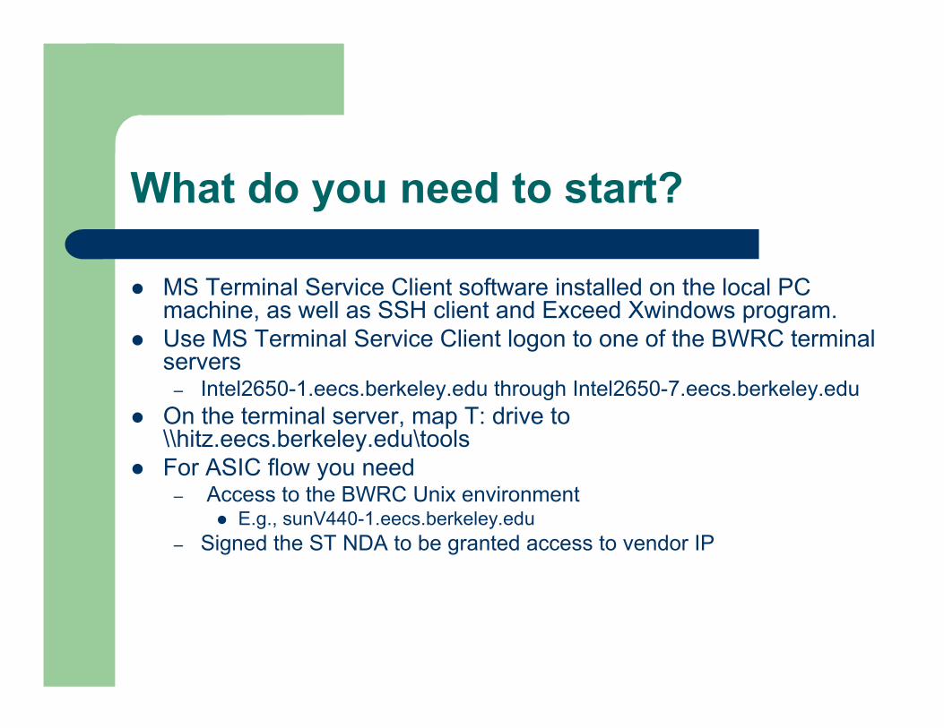
What do you need to start?
� MS Terminal Service Client software installed on the local PC machine, as well as SSH client and Exceed Xwindows program.
� Use MS Terminal Service Client logon to one of the BWRC terminalservers
– Intel2650-1.eecs.berkeley.edu through Intel2650-7.eecs.berkeley.edu� On the terminal server, map T: drive to
\\hitz.eecs.berkeley.edu\tools� For ASIC flow you need
– Access to the BWRC Unix environment� E.g., sunV440-1.eecs.berkeley.edu
– Signed the ST NDA to be granted access to vendor IP

Starting a new project
� SSH to a Unix machine (e.g., sun450-1)� $ tcsh� $ setenv PATH /tools/insecta/current/bin:$PATH� $ setenv DISPLAY your_machine:0.0
– This may be set automatically if SSH X11 tunneling is enabled.� $ cd /tools/designs/your_work_dir
– EG: /tools/designs/BEE/users/login_name– Avoid using your home directory – space is limited!
� $ mk_insecta_project tut1– This creates the tut1 directory with several design subdirectories.
� $ cd tut1� The same directory can be accessed from the PC side as
//hitz/Designs/your_work_dir/tut1� And then return to the PC side for a little while…

Starting Matlab/Simulink
� First start Matlab, then type “simulink” in the command window
� Type “path” in the command window and verify \\hitz\designs\BEE\mlib is included
� Check the “Xilinx Blockset” toolbox is installed in the library browsing window
� Create a new model– File -> New -> Model
How is this Tutorial Organized
� Section 1: Creating and Simulating a Model� Section 2: Tag and Route the Design
conforming to BEE architecture� Section 3: Generating FPGA Bit File Using
BEE_ISE Tool� Section 4: Download and Emulate Design on
BEE Hardware� Section 5: ASIC flow basics

Current Section
� Section 1: Creating and Simulating a Model� Section 2: Tag and Route the Design
conforming to BEE architecture� Section 3: Generating FPGA Bit File Using
BEE_ISE Tool� Section 4: Download and Emulate Design on
BEE Hardware� Section 5: ASIC flow basics

Create a System Generator Model
� Drag a “System Generator” block to the design
� Double click on the block to bring up the property dialog
� Choose VirtexE family, XCV2000E-6-fg680 chip
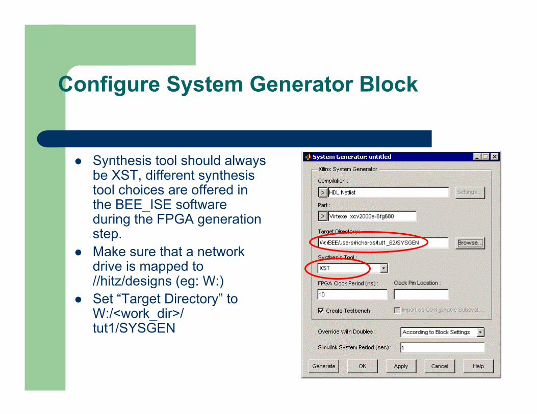
Configure System Generator Block
� Synthesis tool should always be XST, different synthesis tool choices are offered in the BEE_ISE software during the FPGA generation step.
� Make sure that a network drive is mapped to //hitz/designs (eg: W:)
� Set “Target Directory” to W:/<work_dir>/ tut1/SYSGEN
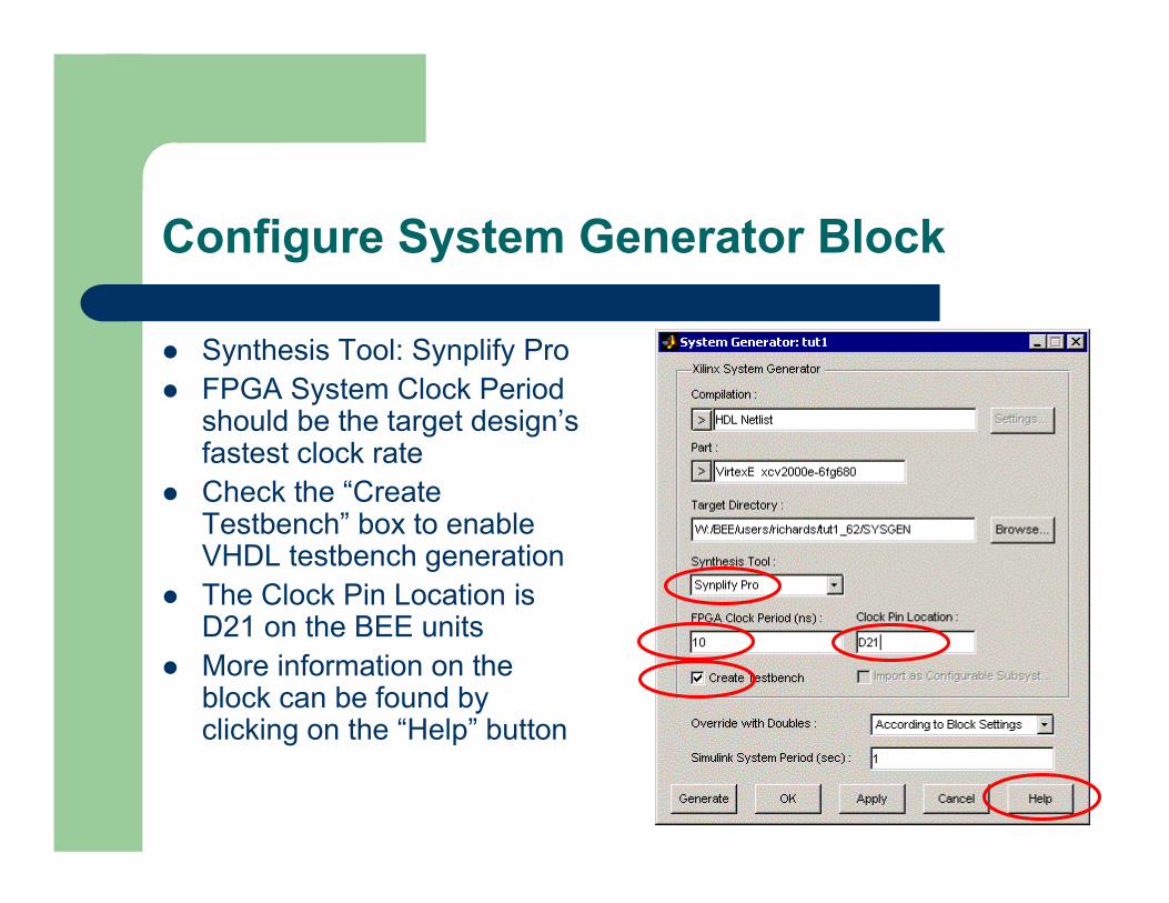
Configure System Generator Block
� Synthesis Tool: Synplify Pro� FPGA System Clock Period
should be the target design’s fastest clock rate
� Check the “CreateTestbench” box to enable VHDL testbench generation
� The Clock Pin Location is D21 on the BEE units
� More information on the block can be found by clicking on the “Help” button

Add More Blocks to the Model
� Drag the “constant”, “counter”, “Register”, “Slice” blocks to the design from the Basic Elements library
� Drag the “Inverter”, “AddSub” block from the Math library
� Now save your model as W:/<work_dir >/ tut1/tut1.mdl
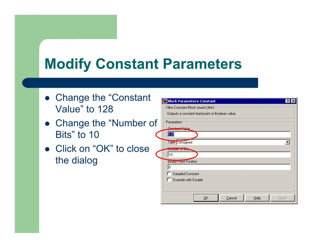
Modify Constant Parameters
� Change the “Constant Value” to 128
� Change the “Number of Bits” to 10
� Click on “OK” to close the dialog
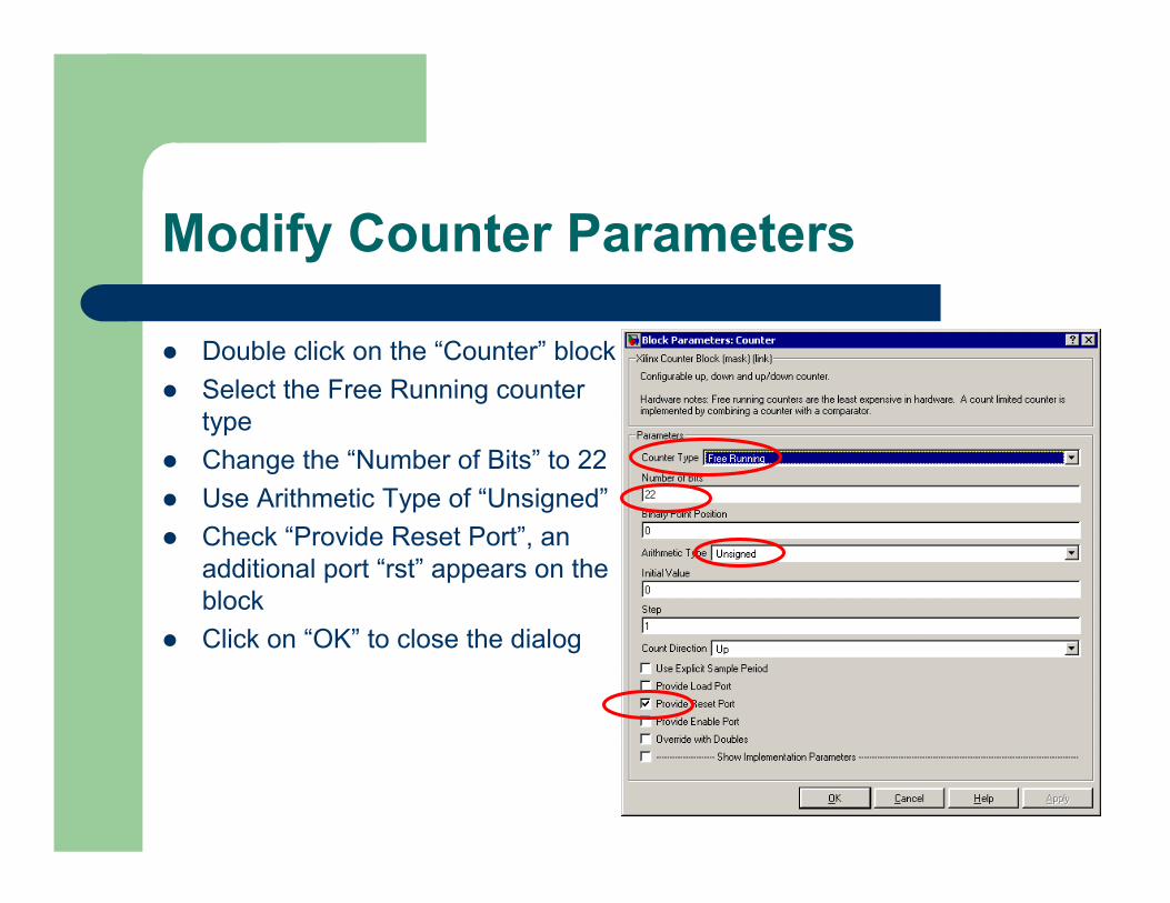
Modify Counter Parameters
� Double click on the “Counter” block� Select the Free Running counter
type� Change the “Number of Bits” to 22� Use Arithmetic Type of “Unsigned”� Check “Provide Reset Port”, an
additional port “rst” appears on the block
� Click on “OK” to close the dialog
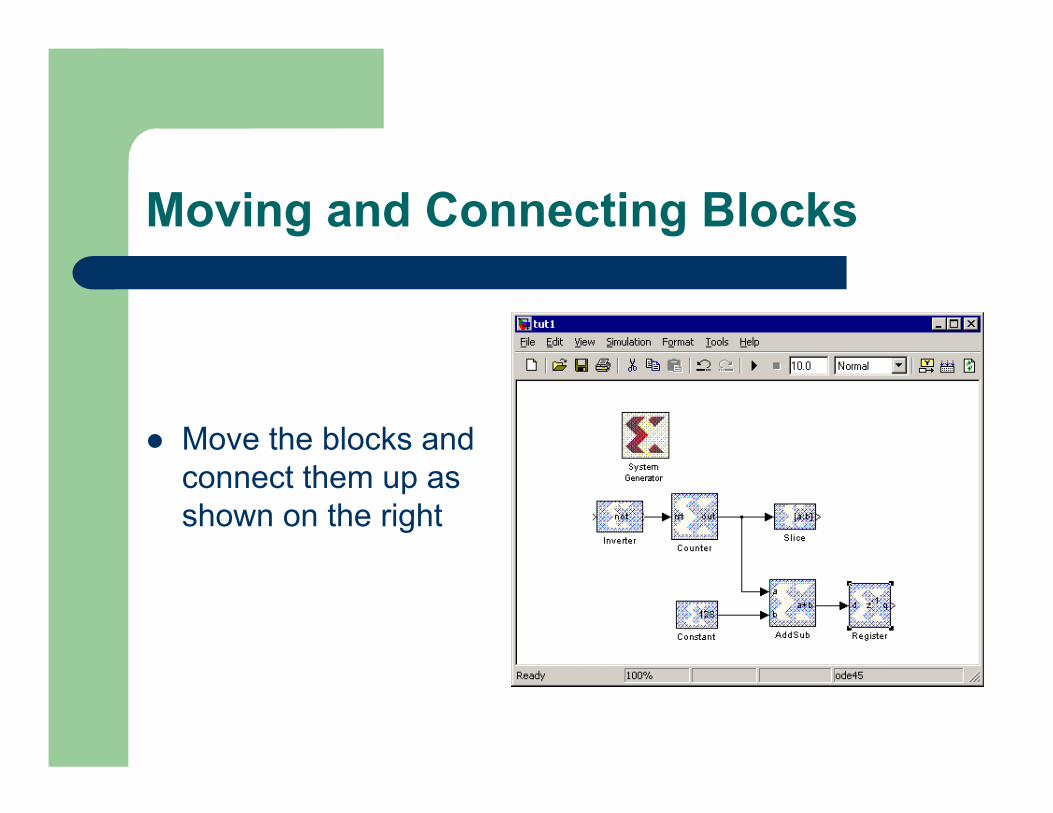
Moving and Connecting Blocks
� Move the blocks and connect them up as shown on the right
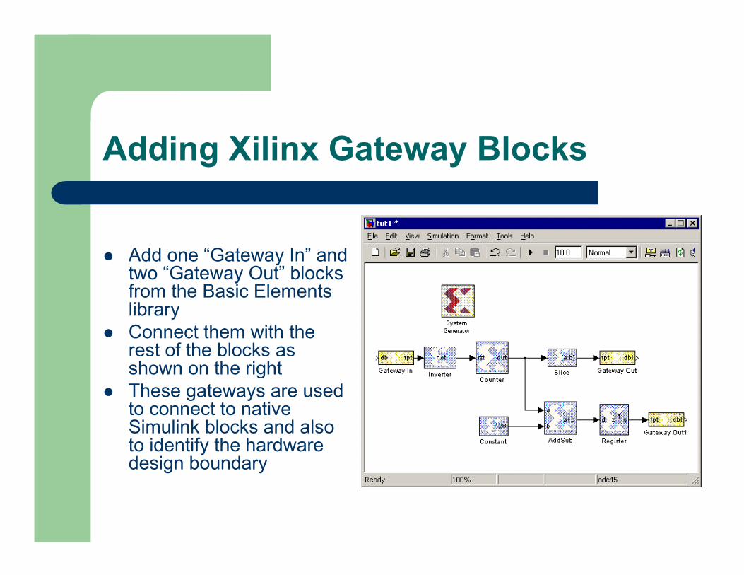
Adding Xilinx Gateway Blocks
� Add one “Gateway In” and two “Gateway Out” blocks from the Basic Elements library
� Connect them with the rest of the blocks as shown on the right
� These gateways are used to connect to native Simulink blocks and also to identify the hardware design boundary
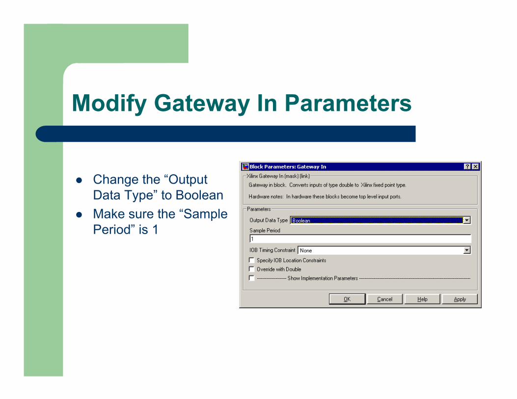
Modify Gateway In Parameters
� Change the “Output Data Type” to Boolean
� Make sure the “Sample Period” is 1

Adding Native Simulink Blocks
� Add one “Pulse Generator” block from Simulink/Sources library, and two “Scope” blocks from Simulink/Sinks library
� Configure the Pulse Generator parameters:– Pulse Type = Sample Based– Period = 1000– Pulse Width = 500– Phase delay = 2
� Place and connect them as shown above

Simulating the Model
� Start the simulation – Simulation -> start
� Double click to open the “Scope1” block, right-click on “Autoscale” (binocular icon), and verify that it looks like the figure on the right
Current Section
� Section 1: Creating and Simulating a Model� Section 2: Tag and Route the Design
conforming to BEE architecture� Section 3: Generating FPGA Bit File Using
BEE_ISE Tool� Section 4: Download and Emulate Design on
BEE Hardware� Section 5: ASIC flow basics

Creating Subsystem
� Click and drag on the model to select all Xilinx library blocks, including the System Generator block, ignoring the Pulse Generator and Scope blocks
� Right click and select “create subsystem”
� This creates a subsystem that will be later targeted to a FPGA

Configure BEE Routes Loading
� Open the Model Properties Dialog
– File -> Model Properties� Click on the Callbacks tab,
and add “load bee_routes.mat;” to Model initialization function
� This loads the BEE routing specific variables to the model at initialization
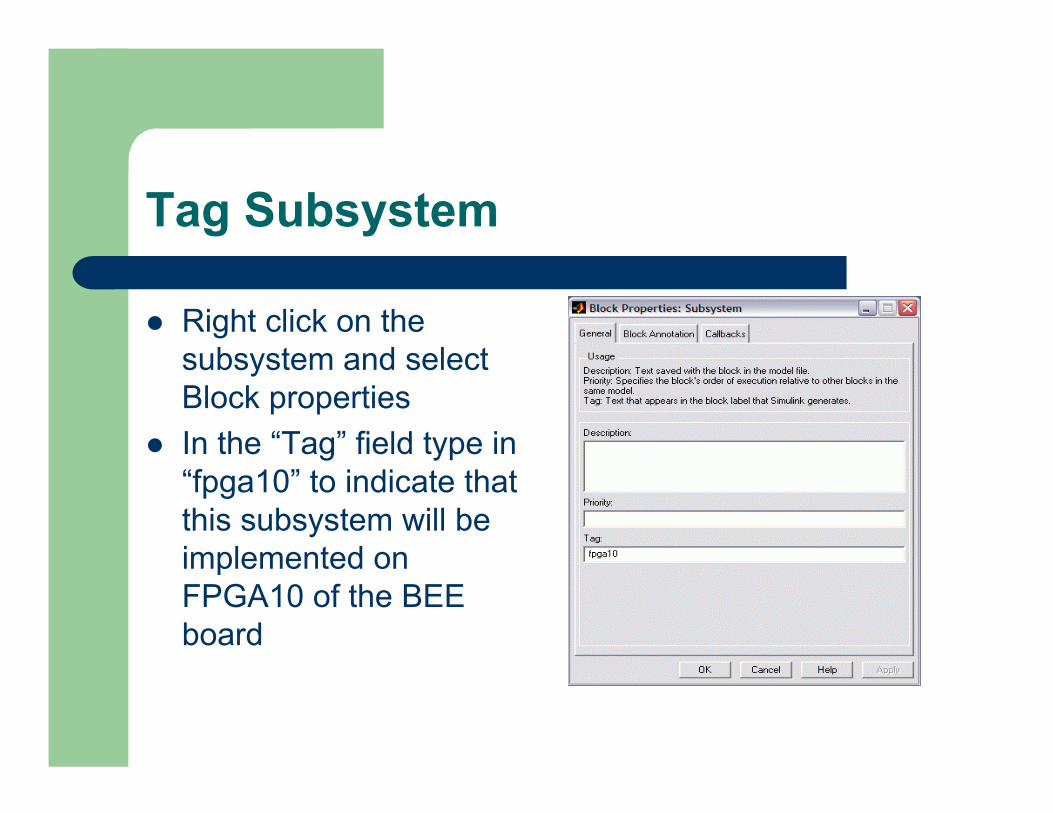
Tag Subsystem
� Right click on the subsystem and select Block properties
� In the “Tag” field type in “fpga10” to indicate that this subsystem will be implemented on FPGA10 of the BEE board
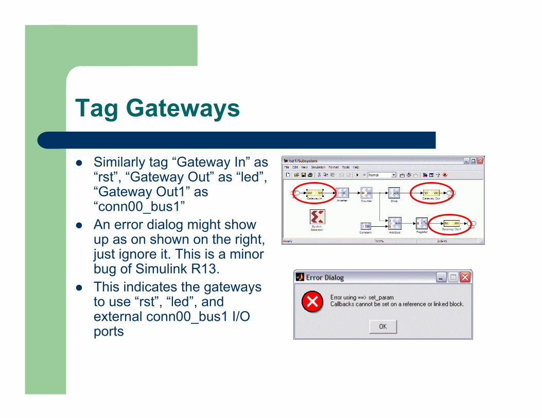
Tag Gateways
� Similarly tag “Gateway In” as “rst”, “Gateway Out” as “led”, “Gateway Out1” as “conn00_bus1”
� An error dialog might show up as on shown on the right, just ignore it. This is a minor bug of Simulink R13.
� This indicates the gateways to use “rst”, “led”, and external conn00_bus1 I/O ports
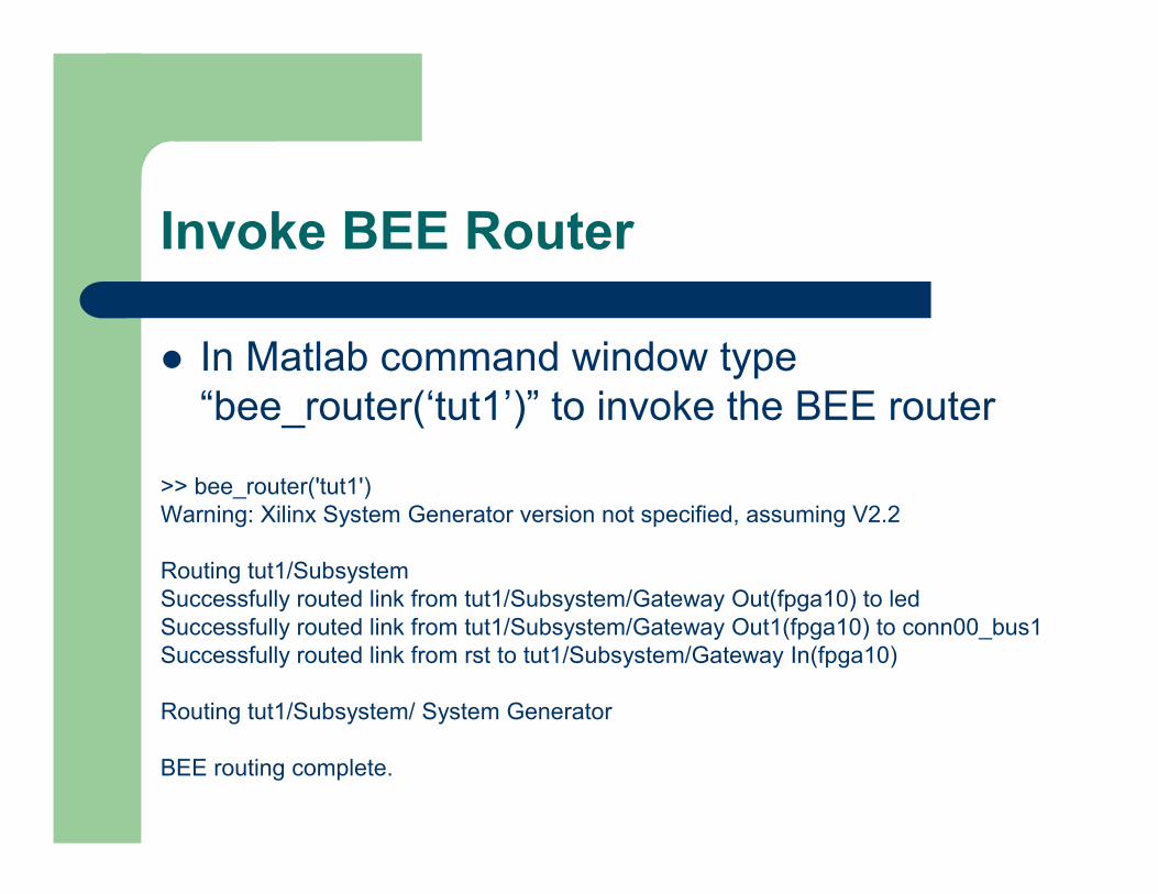
Invoke BEE Router
� In Matlab command window type “bee_router(‘tut1’)” to invoke the BEE router
>> bee_router('tut1')Warning: Xilinx System Generator version not specified, assuming V2.2
Routing tut1/SubsystemSuccessfully routed link from tut1/Subsystem/Gateway Out(fpga10) to ledSuccessfully routed link from tut1/Subsystem/Gateway Out1(fpga10) to conn00_bus1Successfully routed link from rst to tut1/Subsystem/Gateway In(fpga10)
Routing tut1/Subsystem/ System Generator
BEE routing complete.
Current Section
� Section 1: Creating and Simulating a Model� Section 2: Tag and Route the Design
conforming to BEE architecture� Section 3: Generating FPGA Bit File Using
BEE_ISE Tool� Section 4: Download and Emulate Design on
BEE Hardware� Section 5: ASIC flow basics

Invoke System Generator
� Save the Model� Double click on the System
Generator block� Click on the “Generate” button to
invoke System Generator� This creates the necessary VHDL
files and project files� NEW for returning users (12/2003):
The bee_mc_gen command was formerly run at this point, and is no longer needed for XSG 3.1 and newer.
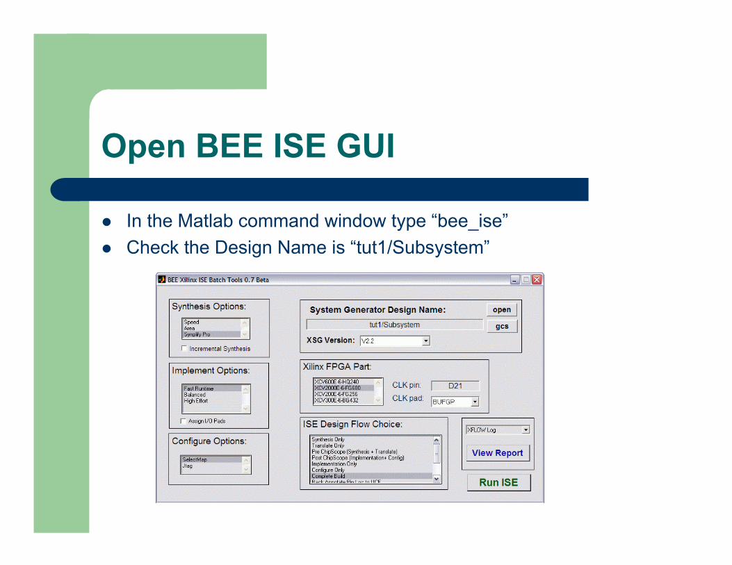
Open BEE ISE GUI
� In the Matlab command window type “bee_ise”� Check the Design Name is “tut1/Subsystem”

Running BEE ISE
� Select “Complete Build” as the Design flow choice, this will synthesize, implement, and generate the FPGA bit file
� Click on the “Run ISE” button to invoke the tools

VHDL Simulation
� If VHDL simulation is desired, click on one of the three simulation flow choices, then click on Run ISE to invoke ModelSim for VHDL simulation
– Behavioral VHDL Simulation can be run right after invoking System Generator– Post Translate VHDL Simulation require Synthesis and Translate steps to be run first– Post PAR VHDL Simulation require Synthesis and Implementation steps to be run first
Current Section
� Section 1: Creating and Simulating a Model� Section 2: Tag and Route the Design
conforming to BEE architecture� Section 3: Generating FPGA Bit File Using
BEE_ISE Tool� Section 4: Download and Emulate Design on
BEE Hardware� Section 5: ASIC flow basics
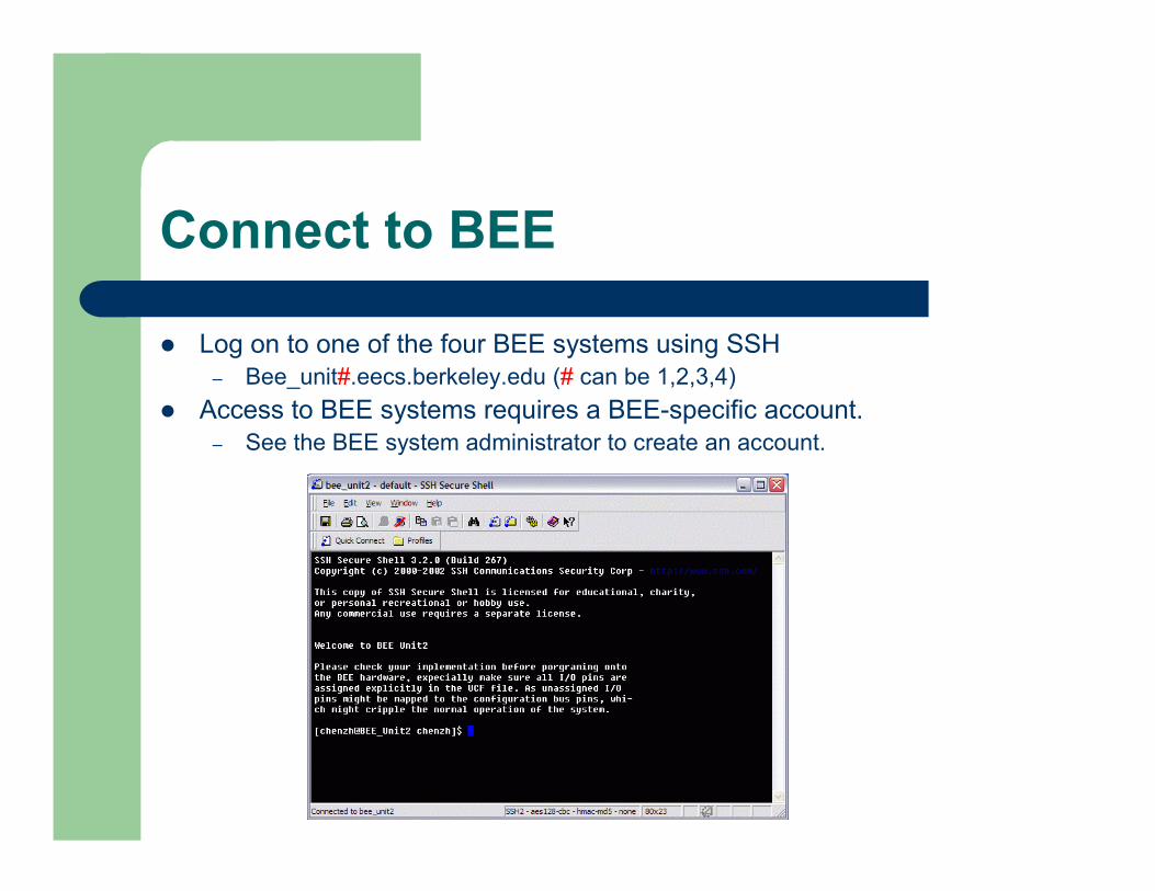
Connect to BEE
� Log on to one of the four BEE systems using SSH– Bee_unit#.eecs.berkeley.edu (# can be 1,2,3,4)
� Access to BEE systems requires a BEE-specific account.– See the BEE system administrator to create an account.
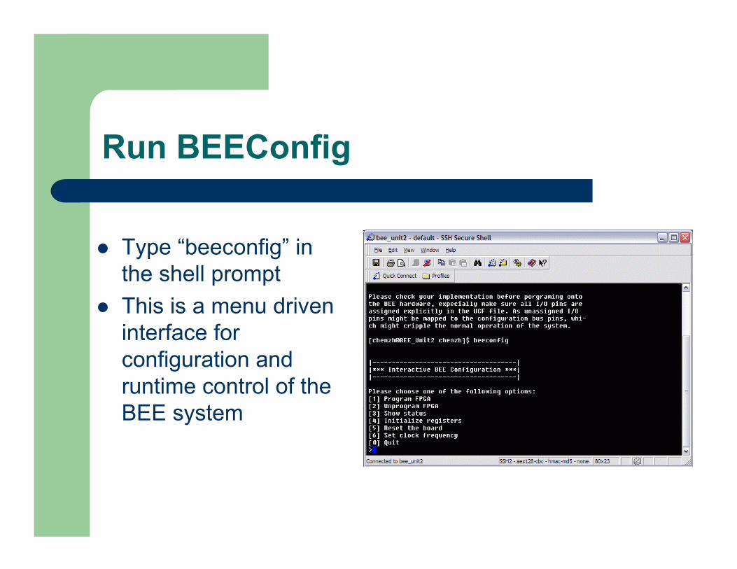
Run BEEConfig
� Type “beeconfig” in the shell prompt
� This is a menu driven interface for configuration and runtime control of the BEE system
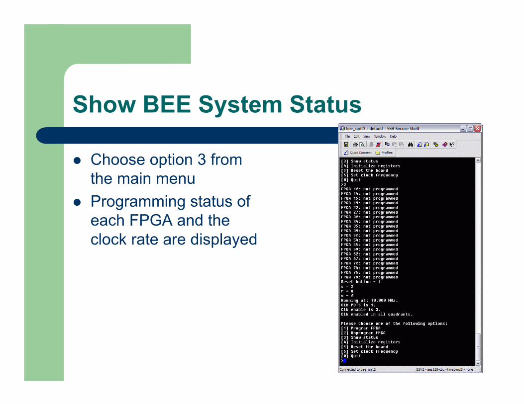
Show BEE System Status
� Choose option 3 from the main menu
� Programming status of each FPGA and the clock rate are displayed
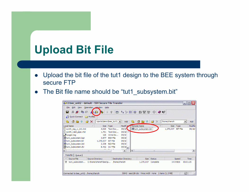
Upload Bit File
� Upload the bit file of the tut1 design to the BEE system throughsecure FTP
� The Bit file name should be “tut1_subsystem.bit”

Program the FPGA
� Select option 1 from the main menu
� Choose the FPGA to be programmed, “10” in this case
� Enter 1 for one hour till expatriation
� After successful programming, the LED on the BEE system FPGA10 will flash
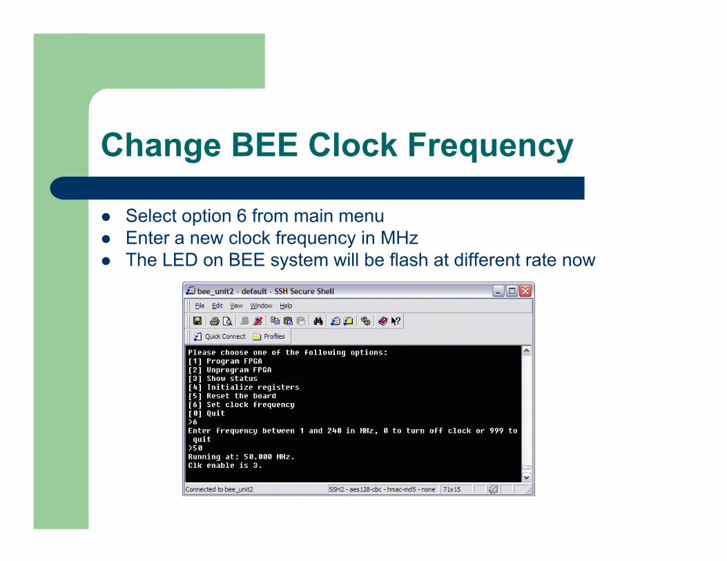
Change BEE Clock Frequency
� Select option 6 from main menu� Enter a new clock frequency in MHz� The LED on BEE system will be flash at different rate now

Current SectionCurrent Section
�� Section 1: Creating and Simulating a ModelSection 1: Creating and Simulating a Model�� Section 2: Tag and Route the Design Section 2: Tag and Route the Design
conforming to BEE architectureconforming to BEE architecture�� Section 3: Generating FPGA Bit File Using Section 3: Generating FPGA Bit File Using
BEE_ISE ToolBEE_ISE Tool�� Section 4: Download and Emulate Design on Section 4: Download and Emulate Design on
BEE HardwareBEE Hardware�� Section 5: ASIC flow basicsSection 5: ASIC flow basics
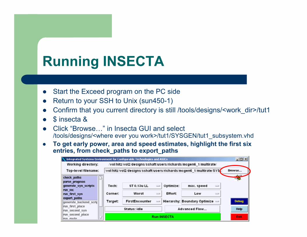
Running INSECTA
� Start the Exceed program on the PC side� Return to your SSH to Unix (sun450-1)� Confirm that you current directory is still /tools/designs/<work_dir>/tut1� $ insecta &� Click “Browse…” in Insecta GUI and select
/tools/designs/<where ever you work>/tut1/SYSGEN/tut1_subsystem.vhd� To get early power, area and speed estimates, highlight the first six
entries, from check_paths to export_paths
Running INSECTA (cont’d)
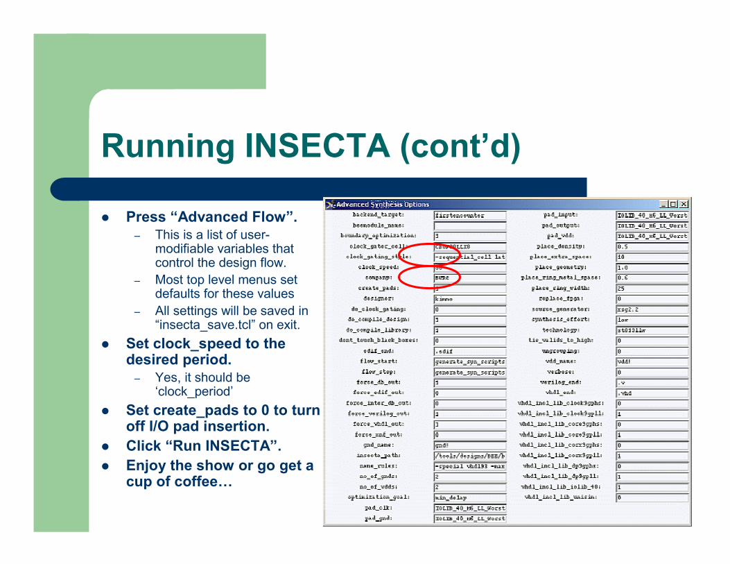
� Press “Advanced Flow”.– This is a list of user-
modifiable variables that control the design flow.
– Most top level menus set defaults for these values
– All settings will be saved in “insecta_save.tcl” on exit.
� Set clock_speed to the desired period.
– Yes, it should be ‘clock_period’
� Set create_pads to 0 to turn off I/O pad insertion.
� Click “Run INSECTA”.� Enjoy the show or go get a
cup of coffee…
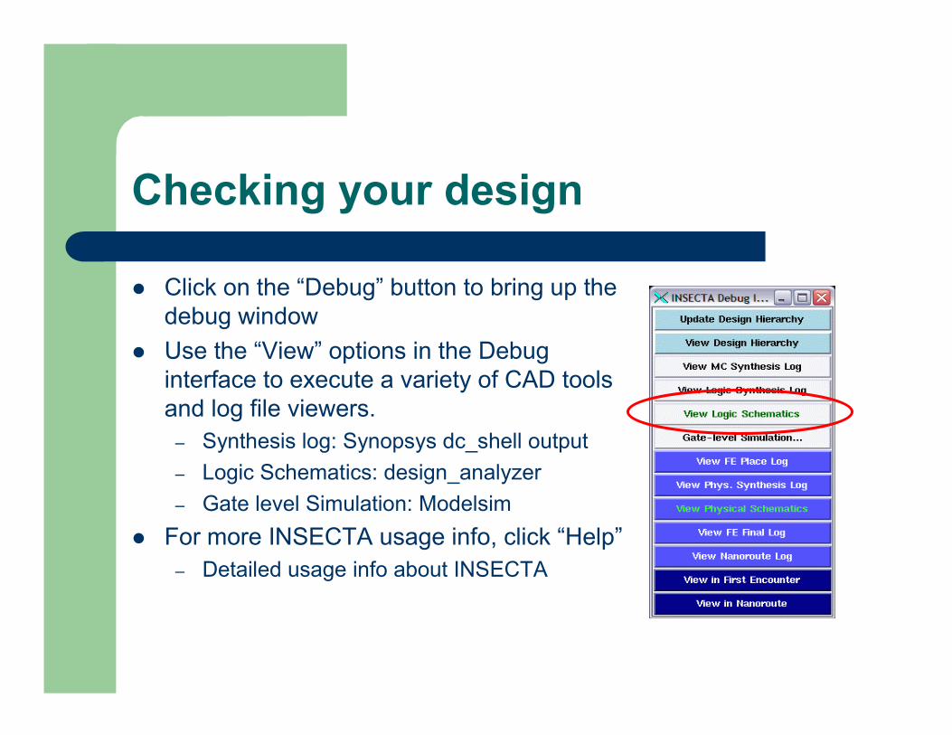
Checking your design
� Click on the “Debug” button to bring up the debug window
� Use the “View” options in the Debug interface to execute a variety of CAD tools and log file viewers.
– Synthesis log: Synopsys dc_shell output– Logic Schematics: design_analyzer– Gate level Simulation: Modelsim
� For more INSECTA usage info, click “Help”– Detailed usage info about INSECTA
Gate-level VHDL Simulation
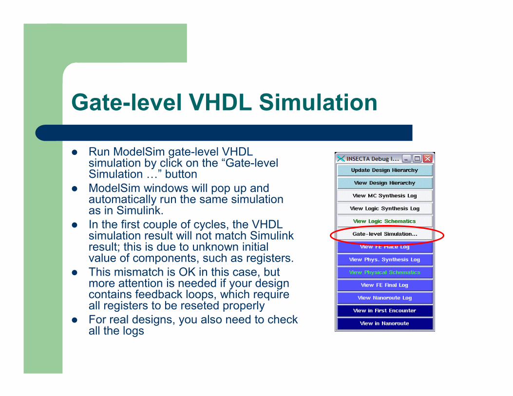
� Run ModelSim gate-level VHDL simulation by click on the “Gate-level Simulation …” button
� ModelSim windows will pop up and automatically run the same simulation as in Simulink.
� In the first couple of cycles, the VHDL simulation result will not match Simulink result; this is due to unknown initial value of components, such as registers.
� This mismatch is OK in this case, but more attention is needed if your design contains feedback loops, which require all registers to be reseted properly
� For real designs, you also need to check all the logs

Congratulations
� You have just finished the first BEE Design Flow tutorial lesson
� For more detailed instruction on how to use the tools introduced, please read the user’s guide or the manual of the tools from the BEE web site