Embed Size (px)
Citation preview

University of Massachusetts Amherst University of Massachusetts Amherst
ScholarWorks@UMass Amherst ScholarWorks@UMass Amherst
Doctoral Dissertations Dissertations and Theses
Fall August 2014
BEAM STEERING CONTROL SYSTEM FOR LOW-COST PHASED BEAM STEERING CONTROL SYSTEM FOR LOW-COST PHASED
ARRAY WEATHER RADARS: DESIGN AND CALIBRATION ARRAY WEATHER RADARS: DESIGN AND CALIBRATION
TECHNIQUES TECHNIQUES
Rafael H. Medina-Sanchez University of Massachusetts Amherst
Follow this and additional works at: https://scholarworks.umass.edu/dissertations_2
Part of the Electrical and Electronics Commons, Electromagnetics and Photonics Commons, Other
Electrical and Computer Engineering Commons, and the Systems and Communications Commons
Recommended Citation Recommended Citation Medina-Sanchez, Rafael H., "BEAM STEERING CONTROL SYSTEM FOR LOW-COST PHASED ARRAY WEATHER RADARS: DESIGN AND CALIBRATION TECHNIQUES" (2014). Doctoral Dissertations. 117. https://doi.org/10.7275/kaba-tq30 https://scholarworks.umass.edu/dissertations_2/117
This Open Access Dissertation is brought to you for free and open access by the Dissertations and Theses at ScholarWorks@UMass Amherst. It has been accepted for inclusion in Doctoral Dissertations by an authorized administrator of ScholarWorks@UMass Amherst. For more information, please contact [email protected].

BEAM STEERING CONTROL SYSTEM FOR LOW-COST PHASEDARRAY WEATHER RADARS: DESIGN AND CALIBRATION
TECHNIQUES
A Dissertation Presented
by
RAFAEL H. MEDINA SANCHEZ
Submitted to the Graduate School of theUniversity of Massachusetts Amherst in partial fulfillment
of the requirements for the degree of
DOCTOR OF PHILOSOPHY
May 2014
Electrical and Computer Engineering

c© Copyright by Rafael H. Medina Sanchez 2014
All Rights Reserved

BEAM STEERING CONTROL SYSTEM FOR LOW-COST PHASEDARRAY WEATHER RADARS: DESIGN AND CALIBRATION
TECHNIQUES
A Dissertation Presented
by
RAFAEL H. MEDINA SANCHEZ
Approved as to style and content by:
David J. McLaughlin, Chair
Stephen J. Frasier, Member
Ramakrishna Janaswamy, Member
Gopal Narayanan, Member
Christopher V. Hollot, Department ChairElectrical and Computer Engineering

This dissertation is dedicated to my wife, Michelle,my children Jeshua, Annia and Sharai,
and my wonderful parents Carmen and Rafael.

ACKNOWLEDGMENTS
Completing my dissertation has been a tremendous personal achievement, which would
not have been possible without the support and contribution of many people. I would first
like to express my deepest gratitude to my adviser Dr. David McLaughlin, who gave me
the opportunity to be a part of CASA project and who supported in every moment the
initiative of a “CASA phased array radar”. I would like to thank Eric Knapp for his help
in discussing the technical aspect of the project and overall guidance. I also wish to thank
my good friend Jorge Salazar for developing the passive array and his enormous help in the
assembly and testing of the phased array.
I would also like to extend my gratitude to Dr. Steve Frasier, Dr. Ramakrishna
Janaswamy, and Dr. Gopal Narayanan for serving as my committee members. My spe-
cial thanks to Dr. Frasier for his involvement and valuable contribution in the solid state
radar group. I also want to thank Dr. Daniel Schaubert for teaching me all the technical
background about phased array and for facilitating the anechoic chamber to measure the
antenna.
I am thankful for the help and support of all members of CASA organization, Susan
Lanfare, Janice Brickley, Marci Kelly, and Apoorva Bajaj, who provided all the technical
and administrative support to the project.
My gratitude also goes to all members of the Microwave Remote Sensing Laboratory
for all their support. My special thank to my friend Jorge Trabal for being a valuable
source of information and discussion on radars. I thanks all my friends and colleagues
from MIRSL, especially, Vijey Venkatesh, Krzysztof Orzel, Cristina Llop, Robert Palumbu,
Razi Ahmed, Benjamin St. Peter, Mauricio Sanchez, Tony Hopf, Anthony Swochak, and
Pei Sang. Thanks to Linda Klemyk and Tom Harley for their assistance in administrative
activities and with laboratory equipments.
v

Most important, I would like to thank my family, because if it was not for them, I would
never have made it this far. My wife Michelle and children Jeshua, Annia, and Sharai,
for their love, support, encouragement, and sacrifices during all these years. My mother,
Carmen, who believed in me and did everything she could to send me to a private university.
I also thank her for giving me her love and instilling in me the importance of education and
hard work. My father, Rafael, for helping my mother and always being present to help me
with whatever I needed. How fortunate I am to have them in my life. I dedicate all my
achievements to them.
The work presented in this dissertation was supported primarily by the Engineering
Research Centers Program of the National Science Foundation under NSF Cooperative
Agreement No. 0313747. Any opinions, findings, and conclusions or recommendations
expressed in this material are those of the author and do not necessarily reflect those of the
National Science Foundation.
vi

ABSTRACT
BEAM STEERING CONTROL SYSTEM FOR LOW-COST PHASEDARRAY WEATHER RADARS: DESIGN AND CALIBRATION
TECHNIQUES
MAY 2014
RAFAEL H. MEDINA SANCHEZ
B.E.E., UNIVERSIDAD TECNOLOGICA DE BOLVAR
M.Sc., UNIVERSITY OF PUERTO RICO MAYAGUEZ
Ph.D., UNIVERSITY OF MASSACHUSETTS AMHERST
Directed by: Professor David J. McLaughlin
Phase array antennas are a promising technology for weather surveillance radars. Their
fast beam steering capability offer the potential of improving weather observations and ex-
tending warning lead times. However, one major problem associated with this technology
is their high acquisition cost to be use in networked radar systems. One promising tech-
nology that could have a significant impact in the deployment of future dense networks
of short-range X-band weather radars is the “Phase-Tilt Radar”, a system that uses a
one-dimensional phase scanned antenna array mounted over a tilting mechanism. This
dissertation addresses some of specific challenges that arise in designing and implement-
ing air-cooled, low-cost, one-dimensional phased antenna arrays for phase-tilt radars. The
goal of this work is to develop methods that can lead to reduce the cost and enhance the
performance of this type of systems.
Specifically, the thesis focuses on three concrete areas. The first one is on the develop-
ment of a versatile low-cost beam steering system that can enable dual-polarimetric phased
array radars to operate with high-frequency repetition pulses, difference pulsing schemes,
vii

and modern scanning strategies. In particular, the dissertation will present the development
of critical components and describes the concept of operations of the beam steering system.
The second area is to develop a calibration technique for small phased arrays. The
work focused in finding the calibration settings for the array that best fit to the desired
excitation. The technique provides lower random errors than conventional approaches,
enabling the implementation of radiation patterns with sidelobes closer to the desired level.
Additionally, the technique is extended to solve the gain-drift problem occurring in the
two-way antenna pattern due to the temperature changes.
The third area studies the use of mutual coupling as signal injection technique to main-
tain the calibration of both array and radar. Future air-cooled phased array radars will
require the use internal circuitry to calibrate the aspect of the radar that tends to change
over time. In particular, this work is focused on developing low-cost calibration techniques
to correct the antenna gain and radar constant from effects of temperature changes and
element failures.
viii

TABLE OF CONTENTS
Page
ACKNOWLEDGMENTS . . . . . . . . . . . . . . . . . . . . . . . . . . . . . . . . . . . . . . . . . . . . . . . . . . . v
ABSTRACT . . . . . . . . . . . . . . . . . . . . . . . . . . . . . . . . . . . . . . . . . . . . . . . . . . . . . . . . . . . . . . . vii
LIST OF TABLES . . . . . . . . . . . . . . . . . . . . . . . . . . . . . . . . . . . . . . . . . . . . . . . . . . . . . . . . .xiii
LIST OF FIGURES . . . . . . . . . . . . . . . . . . . . . . . . . . . . . . . . . . . . . . . . . . . . . . . . . . . . . . . xv
CHAPTER
1. INTRODUCTION . . . . . . . . . . . . . . . . . . . . . . . . . . . . . . . . . . . . . . . . . . . . . . . . . . . . . . . .1
1.1 Introduction . . . . . . . . . . . . . . . . . . . . . . . . . . . . . . . . . . . . . . . . . . . . . . . . . . . . . . . . . . . 11.2 Problem Statement . . . . . . . . . . . . . . . . . . . . . . . . . . . . . . . . . . . . . . . . . . . . . . . . . . . . . 51.3 Dissertation Contributions . . . . . . . . . . . . . . . . . . . . . . . . . . . . . . . . . . . . . . . . . . . . . . . 61.4 Dissertation Overview. . . . . . . . . . . . . . . . . . . . . . . . . . . . . . . . . . . . . . . . . . . . . . . . . . . 8
2. FUNDAMENTALS OF PHASED ARRAYS . . . . . . . . . . . . . . . . . . . . . . . . . . . . 10
2.1 Introduction . . . . . . . . . . . . . . . . . . . . . . . . . . . . . . . . . . . . . . . . . . . . . . . . . . . . . . . . . . 102.2 Linear Array . . . . . . . . . . . . . . . . . . . . . . . . . . . . . . . . . . . . . . . . . . . . . . . . . . . . . . . . . . 10
2.2.1 Directive Gain . . . . . . . . . . . . . . . . . . . . . . . . . . . . . . . . . . . . . . . . . . . . . . . . . . 122.2.2 Realized Gain . . . . . . . . . . . . . . . . . . . . . . . . . . . . . . . . . . . . . . . . . . . . . . . . . . 132.2.3 Half-Power Beamwidth . . . . . . . . . . . . . . . . . . . . . . . . . . . . . . . . . . . . . . . . . . 142.2.4 Half-Power Beamwidth for Two-Way Patterns . . . . . . . . . . . . . . . . . . . . . . 152.2.5 Gain of Active Beamformers . . . . . . . . . . . . . . . . . . . . . . . . . . . . . . . . . . . . . . 162.2.6 Total Power Gain of Active Phased Arrays . . . . . . . . . . . . . . . . . . . . . . . . . 17
2.3 Radar Systems . . . . . . . . . . . . . . . . . . . . . . . . . . . . . . . . . . . . . . . . . . . . . . . . . . . . . . . . 19
2.3.1 Radar Equation for Point Target Return . . . . . . . . . . . . . . . . . . . . . . . . . . . 202.3.2 Weather Radar Equation . . . . . . . . . . . . . . . . . . . . . . . . . . . . . . . . . . . . . . . . 21
3. BEAMFORMER AND BEAM STEERING CONTROL SYSTEM . . . . . . 23
3.1 Introduction . . . . . . . . . . . . . . . . . . . . . . . . . . . . . . . . . . . . . . . . . . . . . . . . . . . . . . . . . . 233.2 System Overview . . . . . . . . . . . . . . . . . . . . . . . . . . . . . . . . . . . . . . . . . . . . . . . . . . . . . . 25
ix

3.2.1 Antenna Array . . . . . . . . . . . . . . . . . . . . . . . . . . . . . . . . . . . . . . . . . . . . . . . . . 253.2.2 Antenna Architecture and Construction . . . . . . . . . . . . . . . . . . . . . . . . . . . . 26
3.3 Array Requirements . . . . . . . . . . . . . . . . . . . . . . . . . . . . . . . . . . . . . . . . . . . . . . . . . . . 27
3.3.1 T/R Modules Requirements . . . . . . . . . . . . . . . . . . . . . . . . . . . . . . . . . . . . . . 273.3.2 RF Power Distribution Network Requirements . . . . . . . . . . . . . . . . . . . . . . 283.3.3 Array Pattern Design . . . . . . . . . . . . . . . . . . . . . . . . . . . . . . . . . . . . . . . . . . . . 293.3.4 Excitation Errors . . . . . . . . . . . . . . . . . . . . . . . . . . . . . . . . . . . . . . . . . . . . . . . 303.3.5 Array Built in Test . . . . . . . . . . . . . . . . . . . . . . . . . . . . . . . . . . . . . . . . . . . . . . 343.3.6 Beam Steering Control System. . . . . . . . . . . . . . . . . . . . . . . . . . . . . . . . . . . . 35
3.4 T/R Modules . . . . . . . . . . . . . . . . . . . . . . . . . . . . . . . . . . . . . . . . . . . . . . . . . . . . . . . . . 37
3.4.1 T/R Module Architecture and Design . . . . . . . . . . . . . . . . . . . . . . . . . . . . . 373.4.2 Diversity Switch Design . . . . . . . . . . . . . . . . . . . . . . . . . . . . . . . . . . . . . . . . . . 403.4.3 Control Electronics and Interfacing . . . . . . . . . . . . . . . . . . . . . . . . . . . . . . . . 423.4.4 Module Implementation and Fabrication . . . . . . . . . . . . . . . . . . . . . . . . . . . 423.4.5 Measurements . . . . . . . . . . . . . . . . . . . . . . . . . . . . . . . . . . . . . . . . . . . . . . . . . . 443.4.6 Test Results . . . . . . . . . . . . . . . . . . . . . . . . . . . . . . . . . . . . . . . . . . . . . . . . . . . . 46
3.5 Backplane Board . . . . . . . . . . . . . . . . . . . . . . . . . . . . . . . . . . . . . . . . . . . . . . . . . . . . . . 51
3.5.1 Description . . . . . . . . . . . . . . . . . . . . . . . . . . . . . . . . . . . . . . . . . . . . . . . . . . . . . 513.5.2 Corporate Feed Network . . . . . . . . . . . . . . . . . . . . . . . . . . . . . . . . . . . . . . . . . 53
3.5.2.1 Design and Implementation . . . . . . . . . . . . . . . . . . . . . . . . . . . . . . 533.5.2.2 Results . . . . . . . . . . . . . . . . . . . . . . . . . . . . . . . . . . . . . . . . . . . . . . . . 56
3.5.3 Backplane Bus . . . . . . . . . . . . . . . . . . . . . . . . . . . . . . . . . . . . . . . . . . . . . . . . . . 56
3.5.3.1 Design . . . . . . . . . . . . . . . . . . . . . . . . . . . . . . . . . . . . . . . . . . . . . . . . 563.5.3.2 Implementation . . . . . . . . . . . . . . . . . . . . . . . . . . . . . . . . . . . . . . . . . 623.5.3.3 Measurements . . . . . . . . . . . . . . . . . . . . . . . . . . . . . . . . . . . . . . . . . . 63
3.6 Beam Steering Control System . . . . . . . . . . . . . . . . . . . . . . . . . . . . . . . . . . . . . . . . . . 64
3.6.1 Architecture . . . . . . . . . . . . . . . . . . . . . . . . . . . . . . . . . . . . . . . . . . . . . . . . . . . . 643.6.2 Interfacing Signals . . . . . . . . . . . . . . . . . . . . . . . . . . . . . . . . . . . . . . . . . . . . . . 693.6.3 Serial Communication . . . . . . . . . . . . . . . . . . . . . . . . . . . . . . . . . . . . . . . . . . . 693.6.4 Digital Command . . . . . . . . . . . . . . . . . . . . . . . . . . . . . . . . . . . . . . . . . . . . . . . 70
3.6.4.1 Unicast Commands . . . . . . . . . . . . . . . . . . . . . . . . . . . . . . . . . . . . . 713.6.4.2 Broadcast Command . . . . . . . . . . . . . . . . . . . . . . . . . . . . . . . . . . . . 753.6.4.3 T/R Module Digital Controller . . . . . . . . . . . . . . . . . . . . . . . . . . . 78
3.6.5 System Integration and Test. . . . . . . . . . . . . . . . . . . . . . . . . . . . . . . . . . . . . . 84
x

4. ARRAY CALIBRATION . . . . . . . . . . . . . . . . . . . . . . . . . . . . . . . . . . . . . . . . . . . . . . . 86
4.1 Introduction . . . . . . . . . . . . . . . . . . . . . . . . . . . . . . . . . . . . . . . . . . . . . . . . . . . . . . . . . . 864.2 Theory . . . . . . . . . . . . . . . . . . . . . . . . . . . . . . . . . . . . . . . . . . . . . . . . . . . . . . . . . . . . . . . 89
4.2.1 Array Alignment . . . . . . . . . . . . . . . . . . . . . . . . . . . . . . . . . . . . . . . . . . . . . . . . 894.2.2 Element Calibration . . . . . . . . . . . . . . . . . . . . . . . . . . . . . . . . . . . . . . . . . . . . . 934.2.3 Element Characterization . . . . . . . . . . . . . . . . . . . . . . . . . . . . . . . . . . . . . . . . 97
4.3 Calibration approach based on nearest state algorithm . . . . . . . . . . . . . . . . . . . . . 99
4.3.1 Pattern Prediction . . . . . . . . . . . . . . . . . . . . . . . . . . . . . . . . . . . . . . . . . . . . . 1034.3.2 Beamtable Format . . . . . . . . . . . . . . . . . . . . . . . . . . . . . . . . . . . . . . . . . . . . . 1034.3.3 Internal Temperature Compensation . . . . . . . . . . . . . . . . . . . . . . . . . . . . . . 106
4.4 Experimental Evaluation . . . . . . . . . . . . . . . . . . . . . . . . . . . . . . . . . . . . . . . . . . . . . . 108
4.4.1 Test Equipment Description . . . . . . . . . . . . . . . . . . . . . . . . . . . . . . . . . . . . . 1084.4.2 Scanner Alignment and Antenna Position Error Estimation . . . . . . . . . 1084.4.3 Temperature Characterization . . . . . . . . . . . . . . . . . . . . . . . . . . . . . . . . . . . 1104.4.4 Receive Array Calibration . . . . . . . . . . . . . . . . . . . . . . . . . . . . . . . . . . . . . . . 1144.4.5 Transmit Array Calibration . . . . . . . . . . . . . . . . . . . . . . . . . . . . . . . . . . . . . 119
4.5 Scanning performance . . . . . . . . . . . . . . . . . . . . . . . . . . . . . . . . . . . . . . . . . . . . . . . . . 122
4.5.1 Sidelobes . . . . . . . . . . . . . . . . . . . . . . . . . . . . . . . . . . . . . . . . . . . . . . . . . . . . . 1264.5.2 Beamwidth . . . . . . . . . . . . . . . . . . . . . . . . . . . . . . . . . . . . . . . . . . . . . . . . . . . . 1274.5.3 Beam Pointing Error . . . . . . . . . . . . . . . . . . . . . . . . . . . . . . . . . . . . . . . . . . . 1284.5.4 Active Element Pattern and Pattern Prediction . . . . . . . . . . . . . . . . . . . . 131
4.6 Temperature Compensation . . . . . . . . . . . . . . . . . . . . . . . . . . . . . . . . . . . . . . . . . . . 135
5. INTERNAL CALIBRATION . . . . . . . . . . . . . . . . . . . . . . . . . . . . . . . . . . . . . . . . . . 143
5.1 Introduction . . . . . . . . . . . . . . . . . . . . . . . . . . . . . . . . . . . . . . . . . . . . . . . . . . . . . . . . . 1435.2 Theory . . . . . . . . . . . . . . . . . . . . . . . . . . . . . . . . . . . . . . . . . . . . . . . . . . . . . . . . . . . . . . 146
5.2.1 Monitoring and Calibration Technique . . . . . . . . . . . . . . . . . . . . . . . . . . . . 1465.2.2 Radar Internal Calibration . . . . . . . . . . . . . . . . . . . . . . . . . . . . . . . . . . . . . . 151
5.2.2.1 Calibration Based on Mutual Coupling Measurements . . . . . . 1525.2.2.2 Calibration Based on a Deterministic Model . . . . . . . . . . . . . . . 154
5.3 Experimental Results . . . . . . . . . . . . . . . . . . . . . . . . . . . . . . . . . . . . . . . . . . . . . . . . . 157
5.3.1 Phased Array Calibration by Mutual Coupling Measurements . . . . . . . 1575.3.2 Gain Calibration Due to T/R Module Failures . . . . . . . . . . . . . . . . . . . . . 1615.3.3 Gain Calibration Due to Temperature Changes . . . . . . . . . . . . . . . . . . . . 1715.3.4 Gain Calibration Due to Temperature Changes and T/R Module
Failures . . . . . . . . . . . . . . . . . . . . . . . . . . . . . . . . . . . . . . . . . . . . . . . . . . . . 174
xi

6. SUMMARY AND CONCLUSION . . . . . . . . . . . . . . . . . . . . . . . . . . . . . . . . . . . . . 178
APPENDICES
A. T/R MODULE SCHEMATIC . . . . . . . . . . . . . . . . . . . . . . . . . . . . . . . . . . . . . . . . . 186B. BACKPLANE . . . . . . . . . . . . . . . . . . . . . . . . . . . . . . . . . . . . . . . . . . . . . . . . . . . . . . . . . 192
BIBLIOGRAPHY . . . . . . . . . . . . . . . . . . . . . . . . . . . . . . . . . . . . . . . . . . . . . . . . . . . . . . . . 193
xii

LIST OF TABLES
Table Page
1.1 Key Radar specifications [7]. . . . . . . . . . . . . . . . . . . . . . . . . . . . . . . . . . . . . . . . . . . . . . 3
3.1 T/R module requerements. . . . . . . . . . . . . . . . . . . . . . . . . . . . . . . . . . . . . . . . . . . . . . 28
3.2 Transmit channel performance . . . . . . . . . . . . . . . . . . . . . . . . . . . . . . . . . . . . . . . . . . 38
3.3 Receive channel performance . . . . . . . . . . . . . . . . . . . . . . . . . . . . . . . . . . . . . . . . . . . . 39
3.4 T/R module performance summary at 9.36GHz. . . . . . . . . . . . . . . . . . . . . . . . . . . . 47
3.5 Data structure of sequence table . . . . . . . . . . . . . . . . . . . . . . . . . . . . . . . . . . . . . . . . 68
3.6 Digital controller interface signals. . . . . . . . . . . . . . . . . . . . . . . . . . . . . . . . . . . . . . . . 69
3.7 First word in unicast command . . . . . . . . . . . . . . . . . . . . . . . . . . . . . . . . . . . . . . . . . 71
3.8 Register address . . . . . . . . . . . . . . . . . . . . . . . . . . . . . . . . . . . . . . . . . . . . . . . . . . . . . . . 71
3.9 Write Port Command. . . . . . . . . . . . . . . . . . . . . . . . . . . . . . . . . . . . . . . . . . . . . . . . . . 72
3.10 Write memory command. . . . . . . . . . . . . . . . . . . . . . . . . . . . . . . . . . . . . . . . . . . . . . . . 73
3.11 Write address register command. . . . . . . . . . . . . . . . . . . . . . . . . . . . . . . . . . . . . . . . . 74
3.12 Read temperature register. . . . . . . . . . . . . . . . . . . . . . . . . . . . . . . . . . . . . . . . . . . . . . 75
3.13 Write sequence table. . . . . . . . . . . . . . . . . . . . . . . . . . . . . . . . . . . . . . . . . . . . . . . . . . . 76
3.14 Sequence table for Single polarization. . . . . . . . . . . . . . . . . . . . . . . . . . . . . . . . . . . . 76
3.15 Sequence table for dual pol - dual PRT. . . . . . . . . . . . . . . . . . . . . . . . . . . . . . . . . . . 77
3.16 Sequence table for dual pol - dual PRF . . . . . . . . . . . . . . . . . . . . . . . . . . . . . . . . . . 77
3.17 Sequence table for fully polarimetric- single PRT (alternate pulse) . . . . . . . . . . . 77
3.18 Sequence table for fully polarimetric -alternate dwell . . . . . . . . . . . . . . . . . . . . . . . 77
xiii

3.19 Sequence table for single polarization - beam multiplexing . . . . . . . . . . . . . . . . . . 78
4.1 Number of beamtables available in a 4K Memory look up table . . . . . . . . . . . . . 104
4.2 Beamtable data format . . . . . . . . . . . . . . . . . . . . . . . . . . . . . . . . . . . . . . . . . . . . . . . . 105
4.3 Comparison of RMS excitation errors for calibrated array in receive . . . . . . . . . 118
4.4 Comparison of RMS excitation errors for calibrated array in transmit . . . . . . . 121
5.1 Gain deviation due to element failures obtained from radiation patternmeasurements, mutual coupling method, and deterministic model . . . . . . . . 168
5.2 Gain deviation due to temperature changes . . . . . . . . . . . . . . . . . . . . . . . . . . . . . . 174
5.3 Gain deviation due to temperature changes and failed elements . . . . . . . . . . . . 177
xiv

LIST OF FIGURES
Figure Page
2.1 Array configuration of one-dimensional phased array antennas. a) Singleelements. b) Columns of elements . . . . . . . . . . . . . . . . . . . . . . . . . . . . . . . . . . . . 11
2.2 Beamformer networks. a) Transmit array. b) Receive array . . . . . . . . . . . . . . . . . 17
3.1 Beamformer architecture for linear active phased array. . . . . . . . . . . . . . . . . . . . . 27
3.2 Two-way sidelobe level resulting from pattern multiplication of an uniformdistribution and different Taylor distributions. . . . . . . . . . . . . . . . . . . . . . . . . . 31
3.3 Optimal radiation patterns for a 64 element phased array antenna intransmit and receive to achieve low peak sidelobes. . . . . . . . . . . . . . . . . . . . . . 31
3.4 Increase in the peak sidelobe for a 64 element array using a 25 dB Taylordistribution. . . . . . . . . . . . . . . . . . . . . . . . . . . . . . . . . . . . . . . . . . . . . . . . . . . . . . . . 33
3.5 Increase in the peak sidelobe for a 64 element array using an uniformdistribution. . . . . . . . . . . . . . . . . . . . . . . . . . . . . . . . . . . . . . . . . . . . . . . . . . . . . . . . 34
3.6 T/R module block diagram. . . . . . . . . . . . . . . . . . . . . . . . . . . . . . . . . . . . . . . . . . . . . 38
3.7 Pin diode diversity switch. a) Schematic. b) Implementation. . . . . . . . . . . . . . . . 41
3.8 Diversity switch performance as a function of frequency. . . . . . . . . . . . . . . . . . . . . 43
3.9 Photograph of the implemented T/R Module. . . . . . . . . . . . . . . . . . . . . . . . . . . . . . 45
3.10 PCB cross section. . . . . . . . . . . . . . . . . . . . . . . . . . . . . . . . . . . . . . . . . . . . . . . . . . . . . . 45
3.11 Measurement equipment setup for the T/R module evaluation. . . . . . . . . . . . . . . 46
3.12 Average gain and return losses for 64 modules. . . . . . . . . . . . . . . . . . . . . . . . . . . . . 47
3.13 Transmit peak output power and module efficiency versus input power. . . . . . . 48
3.14 Relative gain/phase performance and saturation power loss versus moduletemperature. . . . . . . . . . . . . . . . . . . . . . . . . . . . . . . . . . . . . . . . . . . . . . . . . . . . . . . . 49
xv

3.15 Resolution step as a function of component states. Left: Attenuator. Right:Phase shifter . . . . . . . . . . . . . . . . . . . . . . . . . . . . . . . . . . . . . . . . . . . . . . . . . . . . . . . 50
3.16 Typical switching characteristics of a T/R module.a) RF and DC biaspulse. b) RF pulse at the transmitter output. c) RF pulse at thereceiver output. . . . . . . . . . . . . . . . . . . . . . . . . . . . . . . . . . . . . . . . . . . . . . . . . . . . . 51
3.17 Backplane subsystem. . . . . . . . . . . . . . . . . . . . . . . . . . . . . . . . . . . . . . . . . . . . . . . . . . . 52
3.18 Backplane PCB cross section. . . . . . . . . . . . . . . . . . . . . . . . . . . . . . . . . . . . . . . . . . . . 52
3.19 Backplane board and Beamformer structure. a) Front and rear view ofbackplane board. b) Beamformer assembly . . . . . . . . . . . . . . . . . . . . . . . . . . . . 54
3.20 RF power distribution network. . . . . . . . . . . . . . . . . . . . . . . . . . . . . . . . . . . . . . . . . . 55
3.21 Component and schematic circuit of the RF power distribution network. a)Rat-race coupler. b) 1:16 corporate feed. . . . . . . . . . . . . . . . . . . . . . . . . . . . . . . 55
3.22 Corporate feed layout. . . . . . . . . . . . . . . . . . . . . . . . . . . . . . . . . . . . . . . . . . . . . . . . . . 56
3.23 Return loss for each input port of a 1:16 corporate feed. . . . . . . . . . . . . . . . . . . . . 57
3.24 Insertion loss and insertion phase measured at each branch of a 1:16corporate feed. a) Insertion loss. b) Insertion phase. . . . . . . . . . . . . . . . . . . . . 58
3.25 Multidrop topology. . . . . . . . . . . . . . . . . . . . . . . . . . . . . . . . . . . . . . . . . . . . . . . . . . . . 59
3.26 Communication architecture topology for linear phased array antenna. . . . . . . . 60
3.27 Equivalent circuit for a backplane bus. . . . . . . . . . . . . . . . . . . . . . . . . . . . . . . . . . . . 60
3.28 Backplane bus layout. . . . . . . . . . . . . . . . . . . . . . . . . . . . . . . . . . . . . . . . . . . . . . . . . . . 62
3.29 Assembled beamformer structure. . . . . . . . . . . . . . . . . . . . . . . . . . . . . . . . . . . . . . . . 63
3.30 Serial data transmission in a backplane at 25 Mbps. . . . . . . . . . . . . . . . . . . . . . . . 64
3.31 Eye diagram for bus LVDS backplane at 25 Mbps. . . . . . . . . . . . . . . . . . . . . . . . . . 65
3.32 Block diagram of the key logic modules used in beam steering controlsystem. . . . . . . . . . . . . . . . . . . . . . . . . . . . . . . . . . . . . . . . . . . . . . . . . . . . . . . . . . . . 66
3.33 Timing diagram of representative command/response sequence. . . . . . . . . . . . . . 68
3.34 Transmission of a 16-bit word. . . . . . . . . . . . . . . . . . . . . . . . . . . . . . . . . . . . . . . . . . . 70
3.35 Transmission of write port command. . . . . . . . . . . . . . . . . . . . . . . . . . . . . . . . . . . . . 72
xvi

3.36 Transmission of write memory command. . . . . . . . . . . . . . . . . . . . . . . . . . . . . . . . . . 73
3.37 Transmission of write address register command. . . . . . . . . . . . . . . . . . . . . . . . . . . 74
3.38 Transmission of read temperature command. . . . . . . . . . . . . . . . . . . . . . . . . . . . . . . 75
3.39 Transmission of sequence table. . . . . . . . . . . . . . . . . . . . . . . . . . . . . . . . . . . . . . . . . . 78
3.40 Internal structure of the digital controller core. . . . . . . . . . . . . . . . . . . . . . . . . . . . . 79
3.41 Serial receiver and transmit interface flow chart. . . . . . . . . . . . . . . . . . . . . . . . . . . . 80
3.42 Command controller flow chart. . . . . . . . . . . . . . . . . . . . . . . . . . . . . . . . . . . . . . . . . . 82
3.43 Photo of the beamformer network mounted in the antenna frame. . . . . . . . . . . . 85
4.1 Array calibration performed with a near field probe measurementsystem. . . . . . . . . . . . . . . . . . . . . . . . . . . . . . . . . . . . . . . . . . . . . . . . . . . . . . . . . . . . 91
4.2 Attenuator and phase shifter performance in a X-band T/R module. . . . . . . . . . 95
4.3 Amplitude and phase calibration algorithm for T/R modules. . . . . . . . . . . . . . . . 97
4.4 Raw gain and phase map for a X-band T/R module at 9.36 GHz. . . . . . . . . . . . 98
4.5 Calibrated gain and phase map for a X-band T/R module at 9.36 GHz. . . . . . . 98
4.6 Amplitude and phase calibration algorithm for phase array system. . . . . . . . . . 102
4.7 Look up table configuration: Left: memory configuration. Right: memorymap. . . . . . . . . . . . . . . . . . . . . . . . . . . . . . . . . . . . . . . . . . . . . . . . . . . . . . . . . . . . . . 105
4.8 Near field probe test system. . . . . . . . . . . . . . . . . . . . . . . . . . . . . . . . . . . . . . . . . . . . 109
4.9 Measurement equipment setup for phased array calibration. . . . . . . . . . . . . . . . . 109
4.10 Webcam-based alignment control system . . . . . . . . . . . . . . . . . . . . . . . . . . . . . . . . 110
4.11 GUI that determine the element position errors and alignment errors . . . . . . . 111
4.12 Measured temperature and Transmission coefficient S21 as a function oftime and different fan voltages. Top: Temperature. Middle: S21Magnitude. Bottom: S21 phase. . . . . . . . . . . . . . . . . . . . . . . . . . . . . . . . . . . . . . 112
4.13 Relative gain, phase and saturation power performance versus moduletemperature. . . . . . . . . . . . . . . . . . . . . . . . . . . . . . . . . . . . . . . . . . . . . . . . . . . . . . . 114
xvii

4.14 Measured transmission coefficient S21 for receive array at state zero. Top:Relative amplitude. Bottom: Relative phase . . . . . . . . . . . . . . . . . . . . . . . . . . 116
4.15 Comparison of calibrated transmition coefficiente S21 in receive mode .Top: Amplitude distribution. Bottom: Phase distribution . . . . . . . . . . . . . . 117
4.16 Theoretical and measured azimuth far field patterns at 9.36GHz, derivedfrom Near-Field measurement. Top: H polarization. Bottom: Vpolarization. . . . . . . . . . . . . . . . . . . . . . . . . . . . . . . . . . . . . . . . . . . . . . . . . . . . . . 118
4.17 Average output power and error bars versus input power . . . . . . . . . . . . . . . . . 120
4.18 Measured transmition coefficiente S21 for transmit array at state zero. Top:Amplitude distribution. Bottom: Phase distribution . . . . . . . . . . . . . . . . . . . 121
4.19 Comparison of calibrated transmission coefficient S21 in transmite mode.Top: Relative amplitude distribution. Bottom: Relative phasedistribution. . . . . . . . . . . . . . . . . . . . . . . . . . . . . . . . . . . . . . . . . . . . . . . . . . . . . . . 122
4.20 Theoretical and predicted azimuth far field patterns at 9.36 GHz. Top: Vpolarization. Bottom: H polarization. . . . . . . . . . . . . . . . . . . . . . . . . . . . . . . . 123
4.21 Overlay of 255 far field radiation pattern measurements, derived fromNear-field measurements. Top: Horizontal polarization. Bottom:Vertical polarization . . . . . . . . . . . . . . . . . . . . . . . . . . . . . . . . . . . . . . . . . . . . . . . 124
4.22 Overlay of 47 far field radiation patterns for receive mode, horizontalpolarization. Top: Copolar pattern. Bottom: Cross polar pattern . . . . . . . . 125
4.23 Overlay of 47 far field radiation patterns for receive mode, verticalpolarization. Top: Cross polar pattern. Bottom: Copolar pattern . . . . . . . . 125
4.24 Measured gain envelope for receive horizontal and vertical polarization. . . . . . 126
4.25 Measured phase for main beam peak in receive horizontal and verticalpolarization. . . . . . . . . . . . . . . . . . . . . . . . . . . . . . . . . . . . . . . . . . . . . . . . . . . . . . . 127
4.26 Measured sidelobe peaks versus azimuth scan angles. . . . . . . . . . . . . . . . . . . . . . . 128
4.27 Comparison between theoretical and measured beamwith as a function ofscan angle. . . . . . . . . . . . . . . . . . . . . . . . . . . . . . . . . . . . . . . . . . . . . . . . . . . . . . . . 129
4.28 Measured beam pointing error as a function of scan angle, derived frompatterns with scan angle increments of 0.354o . . . . . . . . . . . . . . . . . . . . . . . . . 130
4.29 Measured beam pointing error as a function of scan angle, derived frompatterns with scan angle increments of 0.0025o. . . . . . . . . . . . . . . . . . . . . . . . 130
xviii

4.30 Overlay of 64 elements pattern measurements, derived from near-fieldmeasurements. . . . . . . . . . . . . . . . . . . . . . . . . . . . . . . . . . . . . . . . . . . . . . . . . . . . . 132
4.31 Average embedded element pattern for V polarization. . . . . . . . . . . . . . . . . . . . . 133
4.32 Average embedded element pattern for H polarization. . . . . . . . . . . . . . . . . . . . . 133
4.33 Comparison between average embedded element pattern and scanned gainin H polarization. . . . . . . . . . . . . . . . . . . . . . . . . . . . . . . . . . . . . . . . . . . . . . . . . . 135
4.34 Overlay of average embedded element pattern (AEP) and 64 radiationpattern measurements. . . . . . . . . . . . . . . . . . . . . . . . . . . . . . . . . . . . . . . . . . . . . . 136
4.35 Comparison between measured and predicted radiation patterns atbroadside. . . . . . . . . . . . . . . . . . . . . . . . . . . . . . . . . . . . . . . . . . . . . . . . . . . . . . . . . 137
4.36 Comparison between measured and predicted scanned gain in receive Hpolarization. . . . . . . . . . . . . . . . . . . . . . . . . . . . . . . . . . . . . . . . . . . . . . . . . . . . . . . 138
4.37 Predicted scanned gain for different beamtables as a function of scanangle. . . . . . . . . . . . . . . . . . . . . . . . . . . . . . . . . . . . . . . . . . . . . . . . . . . . . . . . . . . . . 140
4.38 Predicted gain increment between beamtables tn and t0. . . . . . . . . . . . . . . . . . . . 140
4.39 Scanned gain measuremenst at different temperatures. Derived from 47patterns . . . . . . . . . . . . . . . . . . . . . . . . . . . . . . . . . . . . . . . . . . . . . . . . . . . . . . . . . . 141
4.40 Gain drift with and without temperature compensation. . . . . . . . . . . . . . . . . . . . 142
5.1 Location of reference passive elements on the array aperture. . . . . . . . . . . . . . . . 148
5.2 Simplified block diagram of monitoring technique based on mutual couplingmeasurements. . . . . . . . . . . . . . . . . . . . . . . . . . . . . . . . . . . . . . . . . . . . . . . . . . . . . 149
5.3 Block diagram of an active phased array with tapered amplitudedistribution. . . . . . . . . . . . . . . . . . . . . . . . . . . . . . . . . . . . . . . . . . . . . . . . . . . . . . . 155
5.4 Comparison of mutual coupling measurements, at two differenttemperatures, obtained before and after calibration errors. a) Insertionloss. b) Insertion phase. . . . . . . . . . . . . . . . . . . . . . . . . . . . . . . . . . . . . . . . . . . . . 159
5.5 Gain and phase deviation detected by using mutual coupling technique. a)Gain deviation. b) Phase deviation. . . . . . . . . . . . . . . . . . . . . . . . . . . . . . . . . . . 160
5.6 Amplitude and phase distributions in the array, obtained after initialcalibration, errors occur, and recalibration. a) Amplitude distribution.b) Phase distribution. . . . . . . . . . . . . . . . . . . . . . . . . . . . . . . . . . . . . . . . . . . . . . . 162
xix

5.7 Comparison of radiation patterns measured at the initial calibration, aftererror occurs, and after element calibration. . . . . . . . . . . . . . . . . . . . . . . . . . . . 163
5.8 Measurements of sidelobes at the initial calibration, after error occurs, andafter element calibration, obtained from measured radiationpatterns. . . . . . . . . . . . . . . . . . . . . . . . . . . . . . . . . . . . . . . . . . . . . . . . . . . . . . . . . . 163
5.9 Measurements of beamwidth at the initial calibration, after error occurs,and after element calibration, obtained from measured radiationpatterns. . . . . . . . . . . . . . . . . . . . . . . . . . . . . . . . . . . . . . . . . . . . . . . . . . . . . . . . . . 164
5.10 Comparision of far-field radiation pattern obtained from near-fieldmeasurements and after prediction with mutual couplingmeasurements. . . . . . . . . . . . . . . . . . . . . . . . . . . . . . . . . . . . . . . . . . . . . . . . . . . . . 164
5.11 Mutual coupling measurements before and after T/R module failures. . . . . . . . 166
5.12 Gain deviation in an array with 7 failed elements. . . . . . . . . . . . . . . . . . . . . . . . . 167
5.13 Gain distribution before and after failures. . . . . . . . . . . . . . . . . . . . . . . . . . . . . . . . 167
5.14 Comparison of scanned gain under different failure condition, obtained byradiation pattern measurements and by prediction using mutualcoupling measurements. . . . . . . . . . . . . . . . . . . . . . . . . . . . . . . . . . . . . . . . . . . . . 169
5.15 Comparison of scanned gain under different failure condition, obtained byradiation pattern measurements and by prediction using deterministicmodel. . . . . . . . . . . . . . . . . . . . . . . . . . . . . . . . . . . . . . . . . . . . . . . . . . . . . . . . . . . . 169
5.16 Comparison of scanned gain for the case of an array with initial failures,obtained by far-field radiation pattern and by prediction usingdeterministic model. . . . . . . . . . . . . . . . . . . . . . . . . . . . . . . . . . . . . . . . . . . . . . . . 170
5.17 Maximum sidelobe level for a -25 dB Taylor pattern under different failureconditions. . . . . . . . . . . . . . . . . . . . . . . . . . . . . . . . . . . . . . . . . . . . . . . . . . . . . . . . 171
5.18 Mutual coupling measurements obtained at different operatingtemperatures using two passive elements. . . . . . . . . . . . . . . . . . . . . . . . . . . . . . 172
5.19 Temperature distribution along the T/R modules for different operatingtemperatures. . . . . . . . . . . . . . . . . . . . . . . . . . . . . . . . . . . . . . . . . . . . . . . . . . . . . . 173
5.20 Gain deviation obtained at different operating temperatures using mutualcoupling technique. . . . . . . . . . . . . . . . . . . . . . . . . . . . . . . . . . . . . . . . . . . . . . . . . 173
5.21 Scanned gain at different operating temperatures, obtained by radiationpattern measurements and by prediction using mutual couplingmeasurements. . . . . . . . . . . . . . . . . . . . . . . . . . . . . . . . . . . . . . . . . . . . . . . . . . . . . 175
xx

5.22 Scanned gain at different operating temperatures, obtained by radiationpattern measurements and by prediction using deterministic model. . . . . . . 175
5.23 Effects of temperature and failures on the scanned gain. Curves obtainedby radiation pattern measurements, by prediction using mutual couplingmethod, and by deterministic model. . . . . . . . . . . . . . . . . . . . . . . . . . . . . . . . . . 176
xxi

CHAPTER 1
INTRODUCTION
1.1 Introduction
Long range S-band weather radar networks have been in use for many years, and al-
though they have proved to be extremely useful for weather forecasting and warning service,
their ability for observing severe and hazardous weather phenomena in the lower part of the
atmosphere (< 2 Km) has been limited [1]. Part of the problem is caused by the Earth‘s
curvature and terrain-induced blockage, which prevents these systems from observing more
than 50% of atmosphere below 2 km altitude above ground level [2]. Another difficulty
is that current systems provide slow volume scan update time and observations with low
spatial resolution. In general, today’s long-range radars cannot detect the formation and
full vertical rotation of most tornadoes; also they cannot provide accurate estimation of
precipitation near the ground.
The Engineering Research Center (ERC) for Collaborative and Adaptive Sensing of the
Atmosphere (CASA) was established in 2003 with the vision of researching a new technol-
ogy that could improve the observation, detection, and prediction of weather events at the
lower atmosphere. CASA proposed a revolutionary technology, based on a dense network
of short-range dual-polarized X-band weather radars, that can operate collaboratively and
adaptively to sense the atmosphere [3]. The use of various short-range X-band radars can
overcome the problems of blockage due to the Earth’s curvature and enable high spatial and
temporal resolution observations. The center proved the concept by installing four small
radars in a research network in Oklahoma, each radar using a mechanically scanned an-
tenna with a magnetron transmitter. The network served to demonstrate the technology of
adaptive scanning and high-resolution observations of precipitation, providing scan update
times at intervals of one minute or less. The next step in the evolution of this technology
is to improve radars using active electronically scanned antennas (also called phased array
1

antennas). Advantages obtained from phased array radars (PAR) over the mechanically
scanned radar include rapid beam steering, adaptive scanning, multifunction capability,
and graceful degradation.
Phased arrays offer significant technical advantages compared to other types of radar
systems. Their benefits have been extensively proved in military applications for many
years. However, their use in civil applications has been limited because of their high cost.
Although recent advancements in microwave technology have made phase-array components
more affordable, there remains much more to be done in terms of reducing their cost and
the cost of processes that are used to form arrays, if such technology is to be used in future
networked radar systems. Because of phased array benefits, the weather radar community
has recently started to invest time and resources into this technology. Currently, there is
an ongoing project in the United States that involves multiple government agencies and
academic institutions to study the possibility of updating multiple currently civilian radar
systems (around 500 radars) with a single network of long range Multifunction Phased Array
Radars (MPAR), reducing $3 billion in life cycle cost [4]. Preliminary studies indicates
that the cost of a full MPAR system (single node) will be approximately $11.5 million [5].
Although the implementation of an MPAR network may bring many benefits, the system
still has the limitation of providing of reduced coverage in the lowest 3 km of the atmosphere.
CASA offers an alternative approach to MPAR, the center visualizes that a dense net-
work of 10,000 small phased array radars at 30 km radar spacing may be required to provide
nationwide coverage at 30 km radar spacing. CASA argues that “such network have the
potential to supplement, or perhaps replace large radars” [3]. However, for this concept to
be economically feasible alternative, radars need to be built at dramatically lower cost than
current phased array systems. A special challenge is to develop these radars commercially
at a cost of U.S $50 k per unit (U.S $200 k four per node). To meet the cost criteria,
different architectures for realizing electronically steered arrays have been evaluated includ-
ing frequency-phase, phase-tilt and phase-phase technology. CASA demonstrated through
a feasibility study [6] that both cost and performance requirements can be achieved us-
ing a phase-tilt radar. This type of system uses a one-dimensional phase antenna array
mounted over a tilting mechanism. Such configuration will allow radars to perform elec-
2

tronic scanning in azimuth direction and mechanical scanning in elevation direction. Some
of the features that this technology should have, includes small-aperture, low power, dual-
polarization elements, low profile, and lightweight. Some established specification for these
systems are described in Table 1.1. Their small size and low weight will allow them to be
mounted on small towers having small footprints or used on existing infrastructures such
as communication towers and rooftops, reducing potentially infrastructure costs.
Table 1.1: Key Radar specifications [7].
Parameter Value
Operating frequency 9.3 GHz
Antenna size 1 m x 1 m
Antenna beamwidth 2o x 2o
Maximum range 30 km
Power 10 W to 100 W
Azimuth scan range ± 45o
Elevation scan range 0-56o
The first part of this dissertation presents the development of a beam steering network
that enables the development of low-cost, one-dimensional phased antenna arrays for future
phase-tilt weather radars. Beam steering networks are systems that control the shape and
direction of the formed beam by controlling the gain and phase of radiating elements. They
are also the most expensive system in a phased array because they require the replication
of the RF subunits that control the gain and phase of each element. The RF subunits are
typically known as Transmit/Receive (T/R) modules, active components whose functions
are controlled by amplifiers, phase shifters, and attenuators. Phased array systems are ex-
pensive because of the number and high cost of T/R modules populating the antenna. T/R
module costs can make up about 50% of overall phase array costs [8, 6]. Another key com-
ponent in the construction of beam steering networks is the RF distribution network. These
components have the function of splitting/combining the signal that is transmitted/received
from T/R modules. A beam steering system also requires communication interfaces and
digital control units at level of T/R modules to translate the commands sent from the
beam steering computer into control signals that can interpreted by attenuators and phase
3

shifters. One goal of this dissertation is to reduce cost and improve beam switching speed
of phased array radars. This will be done by working in three areas. The first one is to
use high levels of system integration and low cost manufacturing process. The second one
is to design a low-cost high-speed communication interface capable of reducing intercon-
nect complexity. The third one is to design a fast control architecture for T/R modules.
In addition, cost is also reduced by using low-cost T/R modules that operate in alternate
polarization.
The second part of the dissertation presents a calibration technique for small phased
arrays. For successful beam shaping and beam steering in phased array radars, it is im-
portant to precisely set the gain and phase of each element. Precisely settings can only be
obtained if the array is calibrated in advance. The purpose of the calibration is to com-
pensate the amplitude and phase differences among radiation elements, while allowing the
implementation of the desired excitation function. Amplitude and phase differences can
occur due to natural variance of different RF hardware connected to each element. Also,
amplitude and phase characteristic of T/R modules depend on temperature and usually
tend to change in time. Calibration is necessary because it reduces the array errors, which
in turn, leads to the implementation of radiation patterns with very low sidelobes. The
smaller the array errors, the closer the implemented radiation pattern to the theoretical
pattern will be. However, in practice, array errors are limited by the quantization errors
and variance of bit error in both attenuators and phase shifters. Conventional calibration
methods correct the problems associated with theses errors by using calibration look-up
tables in T/R modules. Although these methods have been effectives in the calibration of
arrays, they do not always provide the best settings to be set in the attenuators and phase
shifters. The goal of the second part of the dissertation is to achieve calibration errors
close to the theoretical minimal than can be achieved in an array. In turn, it will allow the
implementation of more ideal radiation patterns. All the above will be done by means a
calibration algorithm that will search for the attenuator and phase shifter settings that best
fit to desired excitation. Techniques to predict the radiation patterns and to compensate
the two-way antenna gain loss due to temperature changes are also presented.
4

The last part of the dissertation studies various techniques to monitor and calibrate
phased array systems in the field. Phased array systems have long been recognized by their
high reliability [9, 10, 6]. They can operate with a certain number of failed elements and
support a wide range of temperatures. However, failures and temperature fluctuations are
aspects that affect the performance of radars. The effect of failures is to reduce the effec-
tive radiated power and raise sidelobes, while temperature tends to produce fluctuations
in the transmit power and receive gain of phased arrays. In order to avoid errors in the
measurements, phased array radars use internal calibration procedures to maintain their
calibration. Typically, internal calibration is performed using a calibration loop, a system
based on directional couplers that can measure the individual characteristics of each element
[11]. Other methods use mutual coupling measurements as calibration techniques [12, 13].
While the calibration loops tend to increase hardware complexity and cost of phased arrays,
the mutual coupling techniques stand because their simplicity and low hardware require-
ment making them suitable for low-cost phased arrays. In the literature, mutual coupling
techniques have been discussed as techniques to maintain the calibration of radiating ele-
ments and to diagnose failures. However, their use in the calibration of radar parameters
have not been reported or covered. The goal of the last part of the dissertation is to develop
low-cost methods to calibrate the antenna gain and radar constant from variations caused
by temperature changes and element failures. This will be done by using two different
methods, both based on results of mutual coupling measurements obtained from passive
elements within the array aperture. Techniques to maintain the element calibrations and
to predict the radiation pattern in the field are also presented.
1.2 Problem Statement
This research aims to address some of the unique and specific challenges that arise in
designing and implementing air-cooled, low-cost, one-dimensional phased array antennas for
short-range X-band weather radars. Specifically, the research concentrates on the design
of a beam steering system, array calibration, and internal calibration of small low-power
phased arrays. The main goal of this work is to present several various methods that
simultaneously reduce cost and enhance the performance of phased array radar system. This
5

leads us to work on three main objectives: At first, develop a versatile low-cost beam steering
control system that will enable operation of dual-polarimetric phased array radars with high
frequency repetition pulses and modern scanning strategies (for example, beam multiplexing
techniques [14]). Second, develop an optimal calibration method for small phased array
having digital attenuators and phase shifters. The method will find the calibration settings
for radiating elements that best fit to desired excitation, providing lower random excitation
errors than conventional approaches. Finally, a study of the use of mutual coupling as signal
injection technique to maintain both array and radar calibration will be investigated. The
study will be focused in the gain calibration due to the effects of temperature changes and
element failures. This research is the first step towards developing of low cost hardware and
calibration techniques for a future networked radar system.
1.3 Dissertation Contributions
This section presents a list of the main contributions of this dissertation, highlighting
three main areas. The first area is the design a beam steering control system for one-
dimensional phased array antennas. The second area is a calibration technique for phased
arrays. The third area is the internal calibration of phased array systems. The following
items summarize the main contribution of this dissertation.
Versatile low-cost beam steering control system for one-dimensional phased
array antennas
• Develop the requirements for the design of a one-dimensional phased array antenna
for low-cost X-band weather radars.
• Design, implementation, and test of T/R modules for an analog beamformer network.
The beamformer will enable the development of low-cost phase array antennas.
• Design of a backplane board to simplify the interconnection between T/R modules and
other radar subsystem. The backplane includes two RF power distribution networks,
a DC bias network, and a control and communication bus. The design reduces wiring
complexity and cost of arrays by integrating various subsystem in a single board
(which simplifies manufacturing process), and by using low cost PCB materials.
6

• Design and evaluation of a high-speed heavily loaded communication bus for the
control of T/R modules. The bus is capable of driving up to 32 T/R modules in
parallel using communication speeds up 100 Mbps.
• Design and evaluation of a versatile beam steering control system. The control ar-
chitecture is based on a distributed beam steering system, which consists of a central
controller and several element controllers at the level of each T/R module. The control
differs from others architectures in that element controllers are controlled in paral-
lel and synchronously by the central controller, and that element controllers do not
use arithmetic units to compute the amplitudes and phases. The system has been
designed to supports multiple pulsing schemes.
Calibration Technique for Phased Arrays
• Development of a calibration algorithm that finds the best available settings to im-
plement the excitation function of a phased array. While conventional calibration
technique only use the attenuator and phased shifter states that fit to ideal quantiza-
tion states, the proposed technique takes advantage of the variance of attenuator and
phased shifter states and use the discarded value from conventional technique to in-
crease resolution of calibration data. The proposed method allows the implementation
of radiation patterns with sidelobes that are closer to designed sidelobes.
• Development of a novel open loop calibration technique to compensate the two-way
antenna gain from temperature changes. The method is suitable for air-cooled phase
arrays with transmitters operating under compression. Compensation is performed in
the receive array.
• Demonstrate experimentally the similarity between scanned gain of a phased array
and embedded element pattern. It was shown that the scanned gain is affected by the
ripples created the quantization errors, being more notable this effect in the receive
array than the transmit array.
• Present a method to predict the radiation patterns of a phased array antenna by using
calibration data and the embedded element pattern.
Internal Calibration of Low-Cost Phased Array Systems
7

• Demonstrate the use of a monitoring and calibration technique for elements of a phased
array that is susceptible to temperature changes. The technique uses the inherent mu-
tual coupling between active and passive elements as signal injection method to track
and maintain the calibration of active elements. Because of the minimal hardware
requirements and easy implementation, the technique is suitable for low-cost phased
array system.
• Demonstrate a method to estimate the radiation patterns of a phased array from
mutual coupling measurements. The technique is suitable to maintain the antenna
patterns of fielded phased array radars, for example it can be used to estimate the side-
lobe and beamwidth degradation after array maintenance or after diagnosing element
failures.
• Development of a calibration technique based on mutual coupling measurements for
maintaining the internal calibration of low-cost, air-cooled phased array radars. It was
the first time that mutual coupling technique is used to calibrate the radar constant
from variations in the antenna gain and transmit/receive power caused by temperature
changes and failures. The technique eliminates the use of calibration networks and
reduces cost of future arrays.
• Development of a calibration technique based on a deterministic model to maintain the
radar calibration constant of low-cost, air-cooled phased array radars. The model that
takes into account the temperature characteristics of T/R modules and the number of
failed elements presents in array. The model has the advantage that mutual coupling
measurements are not needed to calibrate the gain during precipitation measurement.
1.4 Dissertation Overview
This dissertation describes the design and implementation of a beam steering system for
one-dimensional active phased array antennas, a system that will enable the development
of low-cost solid stated weather radars. It also describes various techniques to calibrate and
maintain the calibration of phased array systems. This thesis is organized as follows.
8

Chapter 2 presents a short description of the basic definitions used in the theory of linear
phased arrays, beamformer network, and radar systems. The correction of the weather radar
equation for use with one-dimensional phased array radars is also presented.
Chapter 3 describes the design and implementation of a low-cost and high-performance
beam steering system for linear phased arrays. A short description of the system archi-
tecture of the CASA phased array antenna is given. This chapter also describes the array
requirements by first describing the radar system requirements. The development of T/R
modules and other array subsystems are also presented. The design of a low-cost hybrid
backplane board that reduces wiring complexity and provides RF signal, bias voltages, and
communication signal to T/R modules is described. The last section describes the design
and implementation of a high-speed beam steering system. Details about system operation,
serial communication, digital commands, and test are given.
Chapter 4 develops a technique to carry out the initial calibration of arrays. The tech-
nique is based on an algorithm that searches in the raw data of each element the best
amplitude and phase settings that minimize the random errors in the excitation. This
chapter provides the theory and experimental demonstration of the calibration technique
in 64 element active phased array. The scanning performance of several array parame-
ters including sidelobes, beamwidth, and beam positioning error are shown. In addition, a
technique to calibrate the two-way antenna gain due to temperature changes is presented.
Chapter 5 presents several techniques based on mutual coupling measurements that can
be used to maintain the calibration of phased array systems. These techniques are suitable
for small low-cost phased array radars due to their reduced cost, easy implementation,
and accuracy. This chapter evaluates the use and limitations of mutual coupling technique
in the monitoring and calibration of radiating elements due to hardware variations and
under the presence of temperature effects. Lastly, two calibration techniques for estimating
and correcting the radar constant due to antenna gain variations are presented. Effects
of temperature changes and T/R module failures on the antenna gain of a receive phased
array antenna isalso studied.
Finally, chapter 6 summarizes the conclusions obtained in this work.
9

CHAPTER 2
FUNDAMENTALS OF PHASED ARRAYS
2.1 Introduction
Phased array antennas can adopt a number of different configurations, including linear,
planar, and circular. This work focuses on linear active phased array antennas whose unit
cell is formed by a subarray of radiating elements, each fed by a transmit and receive module
that can provide amplitude and phase control. Linear phased arrays use the progressive
phase excitation between the elements to scan the antenna beam electronically over one-
dimension, while using the element amplitude distribution to control the pattern shape. The
main advantages offered by phased arrays over conventional systems are increased scanning
speed, high reliability, and multifunction capability. These advantages make the use of
this technology the most logical choice for the next generation weather radars. The use of
linear active phased arrays as a component of future low-cost weather radars is the major
motivator of this work; consequently, this chapter is dedicated to explain the basic concepts
related to the theory of linear phase arrays and how their characteristics can be used in a
radar system.
2.2 Linear Array
Typical configurations used in arrays that perform electronically scanning in one dimen-
sion are shown in Figure 2.1. The array elements can be individual radiators, as shown in
Figure 2.1a, or they can be subarray of radiators, as illustrated in Figure 2.1b. In general,
the excitation of each array element is controlled in amplitude and phase by attenuators
and phase shifters. In addition to the excitation control on each element, there is a relative
phase shift between the waves arriving at the element due to their position in the space and
the angle of arrival of the wave. Under the assumption that all radiating elements have the
10

dx
Amplitude and
Phase control
X
Y
Z
θ
Φ
(a)
dy
dx
Amplitude and
Phase control
(b)
Figure 2.1: Array configuration of one-dimensional phased array antennas. a) Single ele-ments. b) Columns of elements
same element pattern, the far-field array pattern is the summation over all N-elements of
element patterns adjusted by the excitation control and incremental phase shift in space of
each element, that is
f(θ, φ) = f0(θ, φ)N∑n=1
Vnejnkdxsin(θ)cos(φ) (2.1)
where f0(θ, φ) is the common radiation pattern to all elements, Vn is the complex excitation
assigned to each element, k is the free-space propagation constant at the operating frequency,
and dx is the element spacing in x-direction. The pattern f(θ, φ) is maximum when the
far-field contribution from the elements add in-phase. This occurs in the direction (θ0, 0)
by choosing the excitation coefficient , Vn to be
Vn = Ane−jnkdxsin(θ0) (2.2)
This implies that the attenuator and phase shifter at each element must be adjusted to
set the amplitude An and phase αn = −nkdxsin(θ0). In general, the aperture amplitude
distribution controls the beam shape of the pattern, while the phase distribution controls
the pointing direction of the main beam.
11

2.2.1 Directive Gain
The directivity is the characteristic of an antenna that describes how much it concentrate
energy in one direction in preference to radiation in other directions. By definition, the
directivity is given as the ratio of the radiation intensity in a certain direction to the average
radiation intensity, or
D(θ, φ) =U(θ, φ)
Uave(θ, φ)=
|f(θ, φ)|214π
∫ ∫|f(θ, φ)|2sin(θ)dθdφ
(2.3)
where f(θ, φ) is the normalized field pattern of the antenna. Although the above expression
gives the antenna directivity at any angular position, the maximum directivity is the value
that is used to describe the directive of an antenna, which is defined as
D(θ, φ) =4π∫ ∫
|f(θ, φ)|2sin(θ)dθdφ(2.4)
Also from 2.3 in 2.4, one can see that
D(θ, φ) = D|f(θ, φ)|2 (2.5)
For a linear array of N equally spaced isotropic elements, the maximum directivity [15]
is given by
Da =|∑N
n=1An|2∑Nn=1
∑Nm=1 VmVne
j(n−m)kdxsin(θ0)sinc((n−m)kdx)(2.6)
where sinc(x) = sin(x)/x. This expression shows that directivity is a function of the
aperture amplitude distribution, the element spacing, and scan angle. In the particular
case that the element spacing is close to λ/2 (λ= wavelength), the maximum directivity
reduce to (for θ0 = 0)
Da =|∑N
n=1An|2∑Nn=1A
2n
(2.7)
The maximum value that can be obtained from above expression is N , and occurs when all
elements have the same amplitude coefficient.
12

For large planar arrays with a separable aperture distribution, the directivity [16] is
approximately given by the following expression
Da(θ0) = πDxDy cos(θ0) (2.8)
where Dx and Dy are the directivities corresponding to linear arrays with isotropic elements
in the x-direction and y-direction. When scanning to an angle θ0, the directive gain is
reduced to that of the projected aperture. It should be noted that this expression is valid
only for array with not visible grating lobes.
2.2.2 Realized Gain
Theoretically, the realized gain is equal to the maximum directivity reduced by the
radiation efficiency and losses due to impedance mismatches. However in practice, the
realized gain is also affected by the inherent mutual coupling between elements. This effect
modifies the element impedance and produces mismatch losses between T/R modules and
elements. These losses can be taken into account in terms of the reflection coefficients seen
into a typical element (i.e central element) when the entire array is excited [17, 16, 18].
In this case, the realized gain and directivity for a large phased array that scan in one
dimension are related to each other as
Gr(θ0, 0) = εr|f0(θ0, 0)|2(1− |Γ((θ0, 0)|2)DeDa (2.9)
where εr is the radiation efficiency, f0(θ0, 0) is the normalized field pattern form an isolated
element, Γ(θ0, 0) is the active reflection coefficient of a typical element, D is the array
directivity, and De is the element directivity, defined as
De =4πdxdyλ2
(2.10)
in (2.9), the reflection coefficient varies as a function of the scan angle because the resulting
impedance mismatch from the mutual coupling depends on the element excitation.
13

Now, considerer the case when a single element is excited and all other elements are
terminated match loads. The array directivity is equal to unity. From 2.9, the realized gain
reduces to
g0(θ0, 0) = ε|f0(θ0, 0)|2(1− |Γ((θ0, 0)|2)De (2.11)
This is the realized gain for a single element in a large array, sometimes called active
element pattern or embedded element pattern. The above expression shows that the mutual
coupling, which is implicit in the active reflection coefficients, alters the radiation power
pattern of the isolated element. Comparison with (2.9) shows that
Gr(θ0, 0) = g0(θ0, 0)Da (2.12)
If the array is large enough that the individual element pattern are approximately iden-
tica, then the expression shows that gain of the fully excited array is equal to gain of a
single element augmented by the directivity of the array. Other way to represent the eq.
2.11 is substituting the element realized gain by the multiplication of normalized element
pattern, the element directivity, and radiation efficiency, that is
Gr(θ0, 0) = g0n(θ0, 0)εrDeDa (2.13)
where g0n(θ0, 0) = g0(θ0, 0)/g0(0, 0). This formula shows that the array realized gain de-
pends on the shape of normalized element pattern, therefore if the element pattern has dips
or nulls at particular angles, it can be concluded that the full array will have drops in gain
when scanned to these angles.
2.2.3 Half-Power Beamwidth
The beamwidth is defined as the angular separation of the points where the main beam
of the power pattern equals one-half. In a phase array, this parameter can be controlled
by choosing the adequate element amplitude distribution. In general, the principal plane
beamwidths of a rectangular array at broadside are given by
14

θ3,br =0.8858Bxλ
Nxdx(2.14)
φ3,br =0.8858Byλ
Nydy
where θ3,br is the beamwidth on the x− z plane, φ3,br is the beamwidth on the y− z plane,
Bx and By are the beam broadening factors when tapered aperture distributions are used.
While in a uniformly illuminated array this factor is equal to unity, in a -25 dB Taylor
distribution the factor is equal to 1.2.
For other scan angles, the beamwidth increase approximately as 1/cos(θ0). In the case
of a linear array having phase shifters along the x-axis, the beamwidth on the x− z plane
varies as
θ3(θ0) =θ3,brcos(θ0)
(2.15)
while the beamwidth in the orthogonal plane is constant.
2.2.4 Half-Power Beamwidth for Two-Way Patterns
The radiation patterns obtained from a phased array radar is not always same while
transmitting and receiving in the direction of the target. For example, in transmit the
array may use an uniform illumination for transmitting the maximum power available in
transmitter, and then in receive use a tapered illumination for controlling the total sidelobes
in the two-way pattern. In this case, the half-power beamwidth resulting from multiplication
of two is given as
θ2w3 =
√θ23txθ
23rx
θ23tx + θ23rx(2.16)
where θ3tx and θ3rx are the one way half-power beamwidth for transmit and receive patterns
in the x − z plane, respectively. Now, in an antenna that has similar patterns in transmit
and receive, the beamwidth for one-way and two-way patterns are related as
θ1w3 =√
2θ2w3 (2.17)
15

From 2.16 in 2.17, one can see that
θ1w3 =
√2θ23txθ
23rx
θ23tx + θ23rx(2.18)
This is the equivalent half-power beamwidth that would be produced by a linear array when
it transmits and receives with the same radiation pattern. Similarly, if θ3 is substituted by
φ3, 2.18 can be used to determine the beamwidth in the orthogonal plane φ1w3 .
2.2.5 Gain of Active Beamformers
Figure 2.2a depicts a linear array of N-elements configured in transmits. Considerer
that each branch has a complex signal gain gn and that N-way power divider is lossless and
has equal phase in the output terminal. The power divider splits the input power in N
equally portions, where the voltage coupling coefficients is C = 1/√N . Thus, the output
power at each antenna element is Poun,n = g2nPin/N . Now, the total power available in the
antenna output is
Pout =N∑n=1
Pout,n =N∑n=1
g2nPinN
=PinN
N∑n=1
g2n
Hence, the power gain for a transmit beamformer is given by
GBF,tx =PoutPin
=
∑Nn=1 g
2n
N(2.19)
In the case that all branches have the same signal gain g, the beamformer gain is equal
to that of the single branch GBF,tx = g2.
Now, consider the case of linear array configured in receive, see Figure 2.2b. The total
power received in the antenna aperture, Pin, is equally distributed among all array elements
as Pin/N . The received voltage at each radiating element is Vin =√Pin/N . This signal is
amplified and then coupled to the output port Vout,n = gn√Pin/N . The combination of all
power in the output yields
Pout = |N∑n=1
gn
√PinN|2 =
PinN|N∑n=1
gn|2
16

g1
g2
g3
gN-1
gN
Vin
Vin/√N g1Vin/√N
(a)
g1
g2
g3
gN-1
gN
Pout
g12Pin/N Pin/N
(b) Implementation
Figure 2.2: Beamformer networks. a) Transmit array. b) Receive array
the ratio of powers gives the total power gain, which is given as
GBF,rx =PoutPin
=|∑N
n=1 gn|2
N(2.20)
In the case that all branches have the same signal gain g, the beamformer gain is equal to
that of the single branch GBF,rx = g2.
2.2.6 Total Power Gain of Active Phased Arrays
The power gain of an array is by definition associated to the array directivity and antenna
efficiency. However, this concept does not consider that an active phased array has a gain
associated to the array beamformer. The effect of this gain is to increase the radiation
intensity in the space when the array is used as transmitter, or to increase the received
power when the array is used as a receiver. Because of this effect, it results appropriate to
redefine the antenna gain to take into account the beamformer gain.
Consider a transmit array as the one depicted in Figure 2.2a. The radiation pattern
generated by an array having isotropic element at distance r is given by
f(θ, φ) =ejkr
4πr
N∑n=1
gnVin√N
ejnkdxsin(θ)cos(φ)
17

The maximum radiation intensity in the far-field will occur when all the fields radiated
by the element are in phase. This values is proportional to
Umax = |fmax(θ, φ)|2 =1
4πr2
(N∑n=1
gnVin√N
)2
The maximum gain is obtained as
Ga =4πr2Umax
Pin=
(∑Nn=1
gnVin√N
)2V 2in
=
(∑Nn=1 gn
)2N
(2.21)
In the special case that all branches have the same gain g, the total gain is Ga = Ng2 = Dg2,
since directivity is D = N in an uniformly excited array. This result shows that the gain
in an active phased array is augmented by the gain of the beamformer. (2.21) can also be
obtained by multiplying the array directivity and the beamformer gain, that is
Ga = DaGBF (2.22)
where Da is given by (2.7) replacing An = gn. Consequently, the total gain for a transmit
array can be obtained using (2.7) and (2.19) in (2.22)
Ga,tx =
(∑Nn=1 gn,tx
)2∑N
n=1 g2n,tx
∑Nn=1 g
2n,tx
N=
(∑Nn=1 gn,tx
)2N
(2.23)
this is analogous to the expression given in (2.21).The above procedure can also be used
to compute the gain for the receive array. But first, it should be note that in Figure 2.2b
all radiating elements receive the same current. This means the array is receiving with
an uniform illumination before the beamformer. Consequently it is assumed that D = N .
Using this value and (2.20) in (2.22), one can see that
Ga,rx = N
∑Nn=1 g
2n,rx
N2=
(∑Nn=1 g
2n,rx
)N
(2.24)
18

giving a similar expression to that obtained in (2.21). Although the beamformer gains for
transmit and receive array have been defined differently, the expression for the total gain
are similar.
It should be pointed out that equations (2.21),(2.23), and (2.24) represent the ideal gain
of an array and not the realized gain, which includes the term of impedance mismatch or
element pattern. Since we know the effect of the beamformer gain is to increase the array
gain, the realized gain in (2.13) can be written for transmit array and receive array as
Gr,tx(θ0, 0) = g0n,tx(θ0, 0)εr(DeDxDy)GBF,tx = g0n,tx(θ0, 0)εrGa,tx (2.25)
Gr,rx(θ0, 0) = g0n,rx(θ0, 0)εr(DeDxDy)GBF,rx = g0n,rx(θ0, 0)εrGa,rx (2.26)
where
Ga,rx(θ0, 0) = DeDy
(∑Nn=1 gn,rx
)2N
(2.27)
Ga,tx(θ0, 0) = DeDy
(∑Nn=1 gn,tx
)2N
(2.28)
The above expressions are given for a linear array with column of elements (see Figure
2.1b ). In the cases of single radiating elements, Dy is unity.
2.3 Radar Systems
Radars are systems that are capable of measuring the distance, velocities, and transversal
area of objects. Their working principle is based on the transmission of radio waves at a
specific direction in the space and use the returned signal from the illumined scene to
estimate the target properties. The time delay, frequency shift or signal amplitude are
some of the signal characteristics that are used to measure the distance, velocities, and
reflectivity of targets. There are various kinds of radar systems for different purposes. For
weather sensing, the Pulsed-Doppler radar is the most popular system. These systems are
used mainly to locate precipitation, calculate its motion, estimate its category (rain, snow,
hail, etc.), and forecast its future position and intensity.
19

2.3.1 Radar Equation for Point Target Return
The radar equation provides a relationship between the transmitted power Pt, the char-
acteristics of the target, and the receiver power at certain distance from the target. For a
point scatter having backscatter cross section σ, the received power Pr at the receiver input
is given [19] as
Pr =Ptgtgrλ
2σ
(4πr)3r4l2(2.29)
where Pt is the transmit power, gt is the transmit antenna gain, gr is the receive antenna
gain, λ is the wavelength at operating frequency, r is the target range, and l is the system
loss. For mechanically steered radars with dish antennas, the above equation is valid for all
scan angles in azimuth and elevation direction. Whereas for phased array radars, the equa-
tion is not completely true since the scan losses produced when the beam is electronically
steered off-broadside.
To find the appropriate radar equation for a phased array radar that scans in one
dimension, one must substitute (2.26) and (2.25) in (2.29), this yields
Pr(θ0) =Ptgt(θ0, 0)gr(θ0, 0)Ga,txGa,rxλ
2σ
(4πr)3r4l2(2.30)
where the radiation efficiency of antenna has been include in the system losses. It should
be also noted that Pt represents the input power in the transmit array and not the total
transmit power delivered by the phased array as it is established in (2.29). Additionally,
(2.30) shows that received power is a function of scan angle and the element pattern roll-off.
It is obvious that to obtain accurate measurements with this formula, all system parameters
must be measured accurately. Unfortunately, in practice, sometimes some of these parame-
ters are not precisely known (i.e antenna characteristics and losses) and the radar must be
calibrated to obtained the combined effect of these parameters. For example, rearranging
terms, (2.30) can be written as
Pr(θ0) =
(PtGa,txGa,rx
l
)(gt(θ0, 0)gr(θ0, 0)λ2σ
(4πr)3r4l2
)(2.31)
20

The first term on the right side of (2.31) contains radar parameters that are typically
unknown and which contribution must be quantified. The purpose of the calibration is to
determine the combined value of this first term. A classical approach of doing this is to
measure the returned power from a reference target of known backscatter cross section and
known range. Using (2.31), the first term can be computed as
Cs =
(PtGa,txGa,rx
l
)=
((4π)3r4Pr(θ0)
gt(θ0, 0)gr(θ0, 0)λ2σ
)(2.32)
where Cs is the system calibration constant. Note the measurement must be made when
the array beam is pointing to the direction of the reference target.
2.3.2 Weather Radar Equation
The weather radar equation is an extension of the classical radar equation applied to a
distributed target of many scattering elements. The equation is based on the measurement
of the equivalent reflectivity factor Z of precipitation particles from the average received
power that is returned by a volume target concentrated in the main beam. The expression
is defined as
Z =1024ln(2)
cπ3
(λ2l
Ptgtgrτθ3φ3
)(Prr
2
|K|2
)(2.33)
where Z is the radar reflectivity (mm6/m3),Pr is the average receive power (W), τ is the
pulse width (s), c=3x10⁸ m/s is the light speed, K=0.93 is the water dielectric constant,
and θ3 and φ3 are the beamwidth of the one-way antenna pattern. Note that in this formula,
the first term on the right side groups a set of constants, the second term groups the radar
characteristics, and the third term groups the target characteristic.
The weather radar equation for a phased array radar that performs scanning in one-
dimension is obtained by substituting (2.15), (2.25) and (2.26) in (2.33), giving
Z(θ0) =1024ln(2)λ2
cτπ3
(l
PtGa,txGa,rx
)(cosθ0
g0n,tx(θ0, 0)g0n,rx(θ0, 0)θ3,brφ3,br
)(Prr
2
|K|2
)(2.34)
This is the equivalent reflectivity factor obtained from the volume illuminated by the
antenna at the scan angle θ0. The third term in (2.34) represents the scan loss produced
21

by the normalized element pattern and beam broadening effect. When the array uses two
different aperture illuminations in transmit and receive, the beamwidth θ3,br and φ3,br are
the values obtained using (18). The second term represents the system calibration constant
Cs. Finally, it should be pointed out that (34) corrects the reflective factor due to the
scanning loss and broadening effects produced when beam is steered away from broadside,
other effects as field projections [20, 21] are already included in the measured element
pattern. For the case of a polarimetric radar that is tilted in elevation, the reflectivity
factor of each polarization must be corrected by the effect of axis rotation.
The equ. (2.34) can also represented as
Z(θ0) = CR
(cosθ0
g0n,rx(θ0, 0)g0n,tx(θ0, 0)
)(Prr
2) (2.35)
where,
CR =
(1024ln(2)λ2
cτπ3|K|2θ3,brφ3,br
)(l
PtGa,txGa,rx
)(2.36)
is the radar constant, a combination of radar system parameters and physical constants
that determines the proportionality factor between the reflectivity of a target at a given
range and received power.
In general, the reflectivity factor is represented in logarithmic units dBZ, that is
Z[dBZ] = Pr[dBm] + CR[dB] + 20log(r[km]) + 10log(cosθ0) (2.37)
−10log(g0n,rx(θ0, 0)g0n,tx(θ0, 0))
This formula corrects the equivalent reflectivity of one-dimensional phased array radar.
The results obtained by using this formula should be the same to the ones obtained from a
mechanically steered weather radar (assuming zero tilt angle)
22

CHAPTER 3
BEAMFORMER AND BEAM STEERING CONTROL SYSTEM
3.1 Introduction
Phased array antennas are composed by many subsystems including radiating elements,
TR modules, control electronic, communication interfaces, beam steering computer, RF
distribution networks, DC manifold, cooling systems, built-in-test, etc. It is a common
practice to design independently each subsystem in small modules, which are later used
to construct subarray assemblies or build blocks (sometimes called tile or brick [15]) for
the array. Typically, subsystems in a tile or brick construction are interconnected each
other by mean cables (RF cables, ribbon cables, flex cables, etc). Example of type of
construction in phased array that performs scanning only in azimuth plane are given in
[22, 23, 24, 25, 26]. The advantage of this approach is that each subsystem can be tested for
proper operation before the array integration, avoiding the installation of fail components.
The disadvantage is that the lack of high integration between subsystems increases the
fabrication and assembly process steps and increases wiring complexity and cost. Another
approach for realizing the array assemblies is the fabrication of T/R packs (or panels), blocks
that groups 4, 8, or 16 T/R modules with RF distribution networks and control electronic,
all them fabricated in a high integrated PCB [27, 28]. This approach allows cost reduction
of PCB and assembly, and minimize wiring interconnect. The disadvantage is that the
system is expensive to maintain because to replace a failed module it is necessary to replace
an entire T/R pack. Other disadvantage is that mutual coupling (leakage) between T/R
modules limits the use of built-in test based on mutual coupling injection signal techniques
[29].
This chapter describes the design of a low-cost beamformer network for CASA phased
arrays which uses the concept of backplanes utilized in computer systems. Backplane archi-
tecture reduces wiring connections by allowing many daughter cards (T/R modules) to be
23

inserted in slots of a parallel bus. In this work, the backplane board includes all passive sub-
systems needed by the array, which includes RF distribution networks, DC manifolds, and
communication buses. The design approach reduces cost by reducing the fabrication mate-
rials and simplifying the manufacturing process with the integration of various subsystem
in a single board. In addition, T/R modules are fabricated in individual boards to reduce
maintenance cost and provide low cost replacement parts. They also use their own enclo-
sure to reduce the coupling between adjacent modules, which will allow the investigation of
mutual coupling as a calibration technique.
Short-range phased array radars with adaptive and multifunction capabilities require
flexible hardware that allows the system to adapt the scanning strategy according the
target or weather events. It is desired to have systems that can support programmable
pulse repetition frequency (PRF), pulse width, and dwell time, as well as support dual-
polarization, beam-multiplexing, and adaptive scan. In order to support these capabilities,
the beam steering control system must be fast enough to respond the commands sent by the
beam steering computer, which implies the use of high-speed communication interfaces and
microprocessor cores to calculate the attenuator and phase shifter settings that are required
to implement each beam.
Different beam steering control architectures have been used in phased arrays [30, 31].
All them have in common the use of processing units to calculate the T/R module setting
from a phase gradient (phase increment between element), element position and correc-
tion offsets (constant that corrects the hardware errors). Settings must be calculated for
each beam; in a full polarimetric radar this might include the beams TV, TH, RH, and
RV. Computation is performed either by a central processor or by element processors in
T/R modules or subarray. However, there are some disadvantages associated with these
approaches: They requires fast processing units that can add significantly to the array
cost, the processing time to compute and transfer the settings to the attenuator and phase
shifter imposes constraints to radar parameters (i.e. PRF and pulse width), and the trans-
fer of digital commands during radar operation can interfere with RF signals. To overcome
these limitations, a new beam steering control archicture based on look-up tables and state-
machines was designed. The advantages of this system include: flexibility, reduce cost,
24

reduced wiring connection, high speed communication (higher that conventional system),
minimize interference with RF signals, and allow high speed beam switching at very high
PRFs and short pulse widths.
This chapter is organized as follow: Section 2 gives an overview of the array architec-
ture proposed for CASA to developed phased array systems that meet the cost criteria
for implementing low-cost low power X-band weather radars. Section 3 develops the sys-
tem requirements for the beamformer network and beam steering control system of the
array. Section 4 describes the design, implementation approach, and results of T/R mod-
ules. Section 5 explains the design and implementation of RF power distribution networks,
communication bus, and power distribution system. The remaining sections describe the
architecture of beam steering control system, as well as explain the communication and
digital commands used to control the T/R modules.
3.2 System Overview
3.2.1 Antenna Array
A general discussion of the antenna array design is provided in [32]. The radiating
aperture consists of a linear array of 72 vertical subarrays. The inner 64 subarrays are
active elements that are fed by dedicated T/R modules that provide amplitude, phase, and
polarization diversity. Additionally, the aperture has four passive subarrays at both edges
that are used to reduce the edge diffraction effects and non-uniform mutual coupling. The
vertical subarray used in the aperture consists of a linear array of 32 dual-linear-polarized
aperture-coupled microstrip patch antennas that are interconnected by series-fed networks
to each polarization port. The spacing between elements is 17 mm (0.53λ0) in both azimuth
and elevation. This value restricts the maximum scanning angle to ± 62.5o in azimuth,
where the first grating lobe is located. The aperture is fabricated as an array of 4 antenna
tiles (panels) [6], each of which has 18 vertical subarrays in azimuth and 32 elements in
elevation.
25

3.2.2 Antenna Architecture and Construction
Based on the general specifications of the phased array system that were settled on at
an early stage, the aperture was divided in 4 Line Replaceable Units (LRU). Each LRU
consists of an antenna panel having 16 active elements, a beamformer structure having 16
T/R modules, two RF manifolds, a power distributions system, and a serial communication
bus. The decision of splitting the full array aperture into four LRUs is due to the limitation
of fabrication process of the PCB (printed circuit board) and the maximum size of material
used. Panel sizes are limited by manufacturing and assembly capabilities of PCB makers
and PCB assemblers, respectively. Ultimately, the LRU size was chosen to maximize the
material used in the antenna while meeting the requirements by standard PCB fabrication
and assembly processes, which are key to reducing cost. The other key aspect that should
be considered to reduce array fabrication costs is to use high levels of integration in both
electronic components and array subsystems.
In order to reduce the cost and the interconnection complexity between T/R modules
and other array subsystems, key components as RF manifolds, DC distribution systems, and
serial communication buses of each LRU are fabricated into a multilayer PCB. The PCB
design allows the T/R modules to plug directly into a shared high-speed communication bus
and shared power and ground planes, eliminating the use of cables. The connection format
is designed to provide DC, control, and RF signals on the same side of the T/R module.
Although cables are not required to provide DC and control signals to T/R modules, the
interconnections T/R modules and RF manifolds are still realized with conventional RF
cables.
The beamformer architecture used in the linear active phased array is shown in Figure
3.1. The beamformer network is comprised of four beamformer structures, each having an
array of 16 T/R modules and a backplane. The backplane has independent RF, digital,
and DC bias section. The RF section is comprised of two passive corporate feed networks;
one is used as a power divider and the other as a power combiner. The power divider
ports interconnect the radar transmitter with all the transmit modules, while the power
combiner ports interconnect the radar receiver with all the receive modules. The digital
section consists of a scalable and parallel bus that interconnects the 64 T/R modules to
26

PS
A
PS
A
PS
A
PS
A
PS
A
PS
A T/R Modules
Panel1
V H V H V H V H V H V H
Formatter
(Array Controller)
Ethernet Switch
(RS485)
Servo- motor
controller (RS232) PS
A
PS
A
V H V H
RFin RFout
Panel2 Panel3 Panel4
BS1 BS2 BS3 BS4
Backplane bus/ DC distribution system
RF manifolds
Figure 3.1: Beamformer architecture for linear active phased array.
a central array controller [33]. T/R modules are plugged to the backplane bus through a
single multi-pin connector. This connector also allows T/R modules to receive the DC bias
signals from the DC bias section, which consists of various power planes integrated in a
multilayer PCB.
3.3 Array Requirements
3.3.1 T/R Modules Requirements
The requirements that modules should meet for this application are shown in Table
3.1. The key parameters of the transmitter design are a minimum transmit peak output
power of 1 W with a maximum duty cycle of 30% at 9.36 GHz over a minimum of 80 MHz
bandwidth. In the receiver chain, the goal are a minimum gain of 21 dB and less than 5
dB noise figure. The isolation between the antenna ports (H and V polarization) must be
greater than 45 dB. This value is necessary to reduce the polarization errors that can be
induced by the radar system at the polarization switch.
A high resolution control of the phase and gain is desirable to implement the array ex-
citation function with low quantization errors. The required attenuator and phased shifter
steps correspond to 6-bit quantization, the highest-resolution commercially available com-
ponents. To achieve pattern with low sidelobe levels, the attenuator must have a minimum
attenuation range of 10 dB.
27
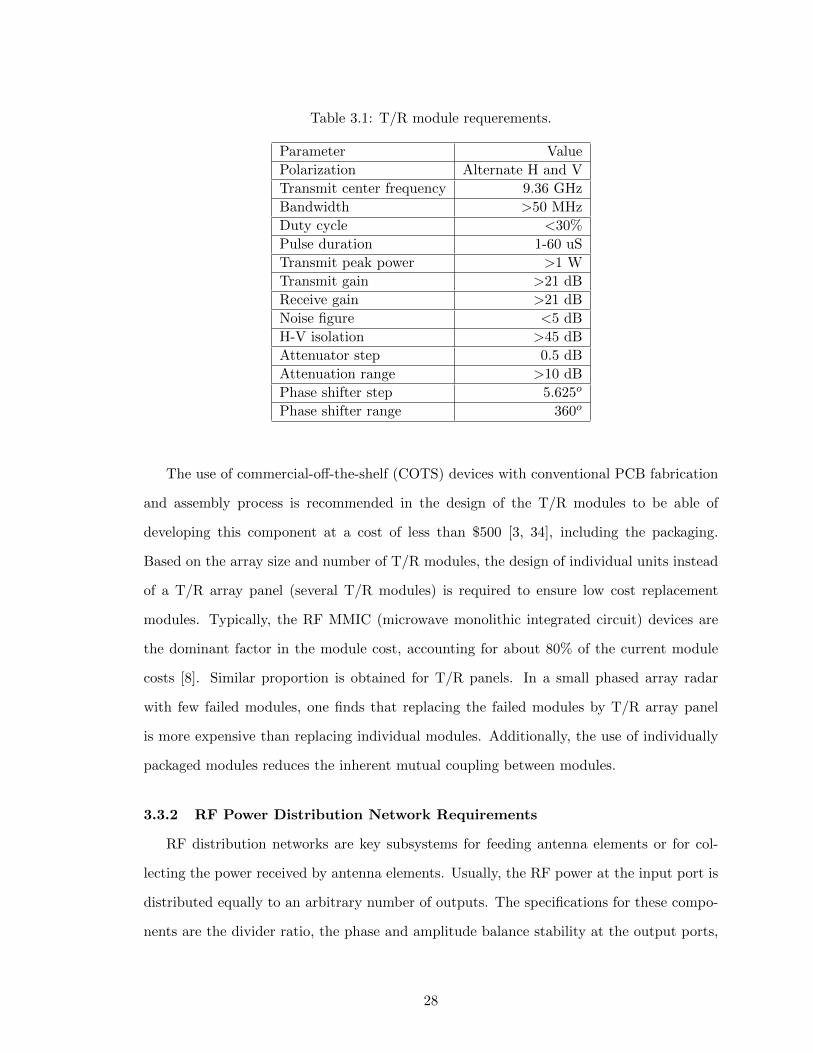
Table 3.1: T/R module requerements.
Parameter Value
Polarization Alternate H and V
Transmit center frequency 9.36 GHz
Bandwidth >50 MHz
Duty cycle <30%
Pulse duration 1-60 uS
Transmit peak power >1 W
Transmit gain >21 dB
Receive gain >21 dB
Noise figure <5 dB
H-V isolation >45 dB
Attenuator step 0.5 dB
Attenuation range >10 dB
Phase shifter step 5.625o
Phase shifter range 360o
The use of commercial-off-the-shelf (COTS) devices with conventional PCB fabrication
and assembly process is recommended in the design of the T/R modules to be able of
developing this component at a cost of less than $500 [3, 34], including the packaging.
Based on the array size and number of T/R modules, the design of individual units instead
of a T/R array panel (several T/R modules) is required to ensure low cost replacement
modules. Typically, the RF MMIC (microwave monolithic integrated circuit) devices are
the dominant factor in the module cost, accounting for about 80% of the current module
costs [8]. Similar proportion is obtained for T/R panels. In a small phased array radar
with few failed modules, one finds that replacing the failed modules by T/R array panel
is more expensive than replacing individual modules. Additionally, the use of individually
packaged modules reduces the inherent mutual coupling between modules.
3.3.2 RF Power Distribution Network Requirements
RF distribution networks are key subsystems for feeding antenna elements or for col-
lecting the power received by antenna elements. Usually, the RF power at the input port is
distributed equally to an arbitrary number of outputs. The specifications for these compo-
nents are the divider ratio, the phase and amplitude balance stability at the output ports,
28

the isolation between different output port and the return loss of each port. The divider
ratio is specified typically as 1 : N , where N is the number of output ports.
Various methods of feeding the array elements are discussed in [35]. The most common
method is the parallel-feed network (also known as corporate feed network), which the
array elements are combined into a network with transmission paths of equal electrical
length. Equal transmission paths leads to equal amplitude and phase signals in the output.
Corporate feed networks are generally preferred in phased arrays because they provide wide
instantaneous bandwidth and good impedance match [36]. Based on these characteristics,
this feeding method was chosen for this work.
The requirements that the corporate feed should meet for this applications are: A
division ratio of 1:16, low insertion loss (<-10 dB), high isolation (<-30 dB), and low-cost.
3.3.3 Array Pattern Design
Weather radars require well designed antenna with very low sidelobes to reduce the error
that may be introduced when the main beam point to a weak reflectivity and the sidelobes
are illuminated by a strong reflectivity. The power received in the main beam is affected
by the power received by the sidelobes, causing errors in the measurements. To reduce the
errors, radars use antennas with sidelobes that are at least 25 dB below the main beam
peak (the two-way sidelobes must be at least 50 dB or better below the main lobe peak).
In a phase array antenna, a 50 dB sidelobe level is obtained when the transmit and receive
aperture use the same tapered amplitude distribution, i.e. a 25 dB Taylor distribution.
The problem of using a tapered amplitude distribution in the transmit aperture is that the
radar cannot transmit at maximum power. The taper distribution limits power of the T/R
modules, reducing the modules efficiency and the radar sensitivity. For instance, a 25 dB
Taylor distribution generates a directivity loss of 0.43 dB and transmit power loss of 2.7 dB
compared to an uniform distribution. Both terms cause a reduction in the radar sensitivity
of 3.1 dB in one-way. In a phased array radar, the use of an uniform distribution in both
transmit and receive apertures can maximize the radar sensitivity. The disadvantage is that
it produces a two-way sidelobes of -26 dB.
29

The most simple and efficient solution for the problem of radar sensitivity and sidelobes
is to use a uniform distribution in the transmit aperture and taper distribution in the receive
array. This criteria allows the transmit array to transmit at maximum power and efficiency
while the receive array can be used to reduce the two-way sidelobes. The question that
arises is what is the best taper function for the receive array?. The question naturally
occurs since the pattern multiplication from a uniform distribution and a highly tapered
distribution for low sidelobe does not provide always the best two-way sidelobe level. Figure
3.2 shows the two-way sidelobes obtained by multiplying the radiation patterns of a uniform
distribution with different Taylor distribution functions in a 64 element array. It shows peak
and average values for different n. The minimum sidelobe peak is -38.8 dB, which is obtained
using a 24 dB Taylor distribution. An average SLL better than 50 dB is obtained when the
designed SLL is specified in the range 20 dB and 34 dB. There is not an improvement in the
two-way sidelobe peak for high values of the designed SLL. Figure 3.3 shows the pattern
multiplication between a uniform distribution and a 24 dB n = 4 Taylor distribution. Note
the beamwidth is wider in the Taylor distribution. This beamwidth gets wider as the
designed SLL is reduced, due to the energy removed from sidelobes is focused in the main
beam. A designed SLL greater than 24 dB produces a radiation patterns whose a main
beams are as wide as the location of the first sidelobe peak of the uniform distribution.
The overlap between the main beam and first sidelobe peak in the pattern of a uniform
distribution results in an increment in the two-way sidelobes, as is show in Figure 3.2.
3.3.4 Excitation Errors
The effect of the random excitation errors and failures on the antenna performance is
to reduce the directivity gain and effective radiate power, and to raise the average sidelobe
level and of some individual sidelobes. Theoretically, one can design the radiation pattern
of an array with any sidelobe level as one desire. However, the random excitation errors
limit the actual sidelobe level that one desires to achieve. The lower and closer the actual
sidelobe level is to the designed sidelobe level, the smaller is the array error required. In
practice, one can deteriorate the designed sidelobe level to achieve the desired sidelobe level
with an acceptable error tolerance [37]. However, reducing the designed sidelobe level much
30

−40 −35 −30 −25 −20−55
−50
−45
−40
−35
−30
−25
SLL for Taylor distribution (dB)
Tw
o−w
ay S
LL (
dB)
SLLpk(n=2)
SLLpk(n=4)
SLLpk(n=6)
SLLav(n=4)
Figure 3.2: Two-way sidelobe level resulting from pattern multiplication of an uniformdistribution and different Taylor distributions.
−30 −20 −10 0 10 20 30−60
−50
−40
−30
−20
−10
0
azimut angle (degree)
Rel
ativ
e M
agni
tude
(dB
)
Tx, uniform distRx, 24dB Taylor distTwo way pattern
Figure 3.3: Optimal radiation patterns for a 64 element phased array antenna in transmitand receive to achieve low peak sidelobes.
31

in excess would increase dramatically the two-way sidelobe level of the radar. To keep low
the two-way sidelobe level, the excitation errors must be low and the designed sidelobe level
not so far from the desired value. For example, to implement a radiation pattern with a
sidelobe peak of 24 dB the array may require a designed sidelobe or 25 dB. However, there
is a probability that designed sidelobe level will exceed the desired value. This probability
can be found from probability density function of the ensemble pattern, which is a Ricean
distribution. The probability of individual sidelobes equal to or less than designed sidelobe
level is given by [37, 15]
P (SLL < SLL0) =
∫ SLL0
0
2.SLL
∆2e
(−SLL2+SLL2
0
∆2
)I0
(2.SLL.SLL0
∆2
).dSLL (3.1)
where SLL0 is the designed sidelobe at some given angle, I0 the modified Bessel function
of the first kind, and ∆2 is the variance of the ensemble pattern sidelobe (also called the
average sidelobe level). The variance for a linear array is given as
∆2 =∆2a + ∆2
p
D0(3.2)
where ∆2a is the amplitude ratio variance normalized to unity, ∆2
p is the phase error variance
in radians squared, and D0 is the array directivity without error is given in (2.7) as
D0 =|∑N
n=1An|2∑Nn=1A
2n
(3.3)
where An is the excitation coefficient for the nth element. For a linear phased array antenna
of 64 element having a 25 dB Taylor distribution, a directivity of 17.7 dB is obtained. The
increase in the peak sidelobe level as a function of the array errors is shown in Figure 3.4.
The curves are obtained from the cumulative probability function (3.1). For example, when
the array error variance is ∆2a = 0.001 (the case when an attenuator of 0.5 dB resolution and
6 bit phase shifter are used) the peak sidelobe level is raised in less than 0.05 dB 50% of the
time, less than 0.6 dB 90% of the time, less than 1.05 dB 99% of the time, and less than 1.5
dB 99.99% of the time. For higher error variances, the increase in the peak sidelobe level is
32
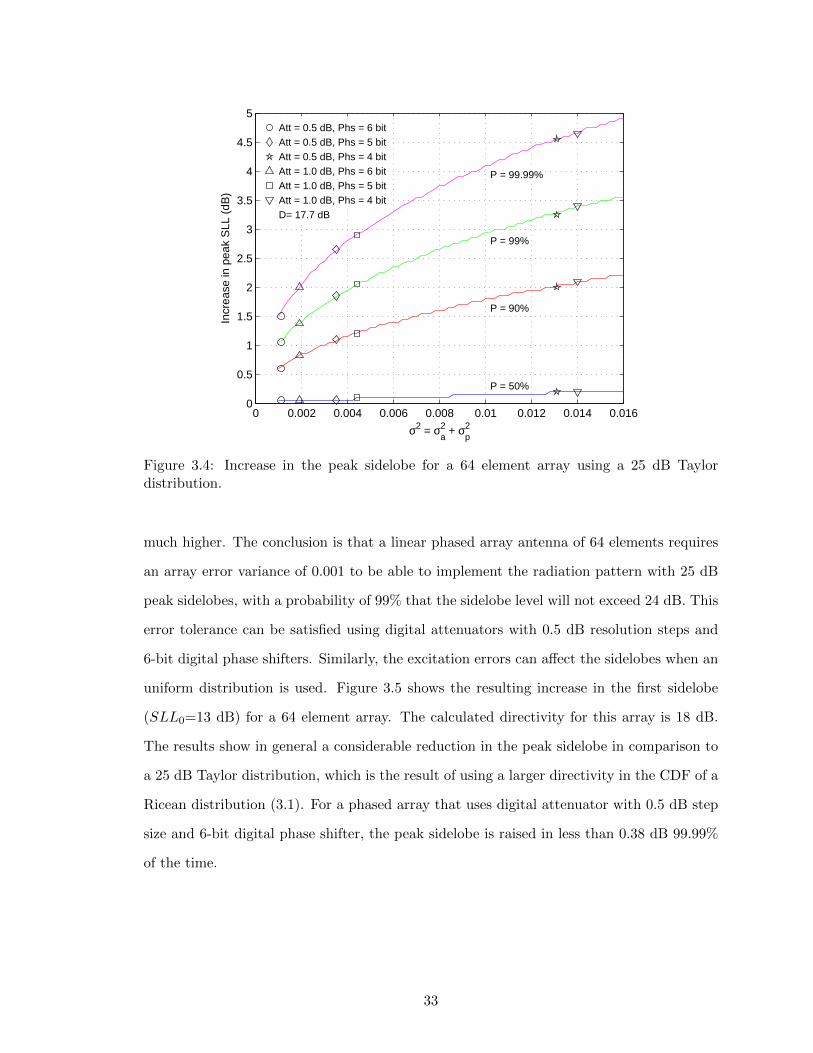
0 0.002 0.004 0.006 0.008 0.01 0.012 0.014 0.0160
0.5
1
1.5
2
2.5
3
3.5
4
4.5
5
σ2 = σa2 + σ
p2
Incr
ease
in p
eak
SLL
(dB
)
P = 99.99%
P = 99%
P = 90%
P = 50%
Att = 0.5 dB, Phs = 6 bitAtt = 0.5 dB, Phs = 5 bitAtt = 0.5 dB, Phs = 4 bitAtt = 1.0 dB, Phs = 6 bitAtt = 1.0 dB, Phs = 5 bitAtt = 1.0 dB, Phs = 4 bitD= 17.7 dB
Figure 3.4: Increase in the peak sidelobe for a 64 element array using a 25 dB Taylordistribution.
much higher. The conclusion is that a linear phased array antenna of 64 elements requires
an array error variance of 0.001 to be able to implement the radiation pattern with 25 dB
peak sidelobes, with a probability of 99% that the sidelobe level will not exceed 24 dB. This
error tolerance can be satisfied using digital attenuators with 0.5 dB resolution steps and
6-bit digital phase shifters. Similarly, the excitation errors can affect the sidelobes when an
uniform distribution is used. Figure 3.5 shows the resulting increase in the first sidelobe
(SLL0=13 dB) for a 64 element array. The calculated directivity for this array is 18 dB.
The results show in general a considerable reduction in the peak sidelobe in comparison to
a 25 dB Taylor distribution, which is the result of using a larger directivity in the CDF of a
Ricean distribution (3.1). For a phased array that uses digital attenuator with 0.5 dB step
size and 6-bit digital phase shifter, the peak sidelobe is raised in less than 0.38 dB 99.99%
of the time.
33

0 0.002 0.004 0.006 0.008 0.01 0.012 0.014 0.0160
0.2
0.4
0.6
0.8
1
1.2
1.4
σ2 = σa2 + σ
p2
Incr
ease
in p
eak
SLL
(dB
) P = 99.99%
P = 99%
P = 90%
P = 50%
Att = 0.5 dB, Phs = 6 bit
Att = 0.5 dB, Phs = 5 bit
Att = 0.5 dB, Phs = 4 bit
Att = 1.0 dB, Phs = 6 bit
Att = 1.0 dB, Phs = 5 bit
Att = 1.0 dB, Phs = 4 bit
D= 18 dB
Figure 3.5: Increase in the peak sidelobe for a 64 element array using an uniform distribu-tion.
3.3.5 Array Built in Test
In general, phased arrays are provided with Built-In-Test (BIT) functions, which contin-
ually monitor the integrity of all of the array elements in the operational environment. BITs
are important components for diagnostic and calibration of arrays. Basically, a built-in-test
measures the element characteristics using a test signal that is generated by an internal
reference sources. Measurements are used to detect failures or hardware drift. To carry out
the measurements, phased arrays must meet three requirements [38]: 1) the ability to turn
on only one T/R module at a time, in either transmit or receive, with other elements are
terminated in match loads, 2) separate transmit and receive beamforming networks, and 3)
a method for injecting the test signal into or out of each module.
Three methods used to inject the test signals into or out all T/R modules are [39, 38]: RF
coupler networks connected to test ports in the T/R modules, near-field antennas mounted
around the periphery of the array, and inherent mutual coupling between elements. In
the two first methods, the array requires additional hardware to implement the built-in-
test, increasing the complexity and cost of the array. In contrast, in the mutual coupling
34

techniques the arrays use their owns elements to couple the test signals. Because of the
minimum hardware requirements and cost, the mutual coupling as a built-in test signal
injection technique is the recommended technique in this work.
3.3.6 Beam Steering Control System
Solid-state phased array radars with adaptive capabilities require flexible control fea-
tures that allow changing the radar parameters during scanning operation, such as antenna
scan patterns, pulse repetition frequency (PRF), pulse width, data collection rates, etc.
Particularly, in short-range adaptive radar system, it is desired to have a PRF and pulse
width that change depending on the situation and needs. A PRF of 1 to 5 KHz (to achieve
an unambiguous range of 30 km) and pulse width of 1 µsec to 60 µsec are typical values
for solid-states radars. To provide these values, the beam steering control system must be
designed with high-speed microprocessors and high-speed communication interfaces that
allow the T/R modules to update rapidly the calibration settings for the next beam. For
example, a polarimetric weather radar operating in alternate mode and using 1 µsec pulse
width (or beam switching) requests beam updates in less than 1 µsec. This implies that
T/R module control signals must be updated in less than 1 µsec (beam update rates higher
than 1 MHz) to switch from transmit beam (i.e. uniform illumination) to receive beam
(i.e.taper illumination). The beam update time must include the beam processing time and
command distribution time to all T/R modules. Beam steering control systems with this
characteristic are not common. In fact, past work has demonstrated that response time of
a beam steering system can be in the range of 5 µsec to 1 msec [40, 10, 41]
The main requirement is to design a low-cost beam steering control system for a dual-
polarimetric radar that can support beam update rates of 1 MHz with minimum ”dead time”
(i.e. the finite time it take to update the T/R module controls for a new beam direction
during which the radar is not transmitting or receiving). The system must also allow pulse-
to-pulse beam switching, a characteristics that radars need to implement scanning strategies
based on beam multiplexing techniques [14]. This technique requires that the beam location
changes every single pulse; which implies that T/R modules settings must be updated every
pulse.
35

The design of the beam steering control system must also include capabilities to control
the element during the calibration. Most calibration techniques require that array has the
ability to turn on only one module at a time, in either the transmit mode or the receive
mode. This feature allows the measurements can be made in a single element while all other
elements are off. During the calibration, the beam steering control system must be able to
control all RF components of a T/R module, for example phase shifter, attenuator, T/R
switch, and V/H switch. The control system must also include digital components such as
memories and registers for storing calibrated data. It must also have the ability to control
the write and read operation of memories and register.
To reduce the cost and wiring complexity in the system, a shared bus topology must
be used to interconnect the digital sections of all T/R modules with the array controller.
Typically this can be done by using communication interfaces the RS-485 standard and
twisted pair cables (CAT5), which allow multidrop communications for up to 32 devices
using speeds lower than 1 Mbps. Other alternative includes the use of LVDS standard and
backplane buses. The advantage of using LVDS is that this standard is used in FPGA
input/output pins, and it does not require external interfaces as the RS-485. Additionally,
it works at speed much higher (up 200 Mbps) than RS-485. While backplane buses are low
cost interfaces, designed typically with microstrip lines, that allow various LVDS devices
can be interconnected in parallel. Based on these characterizes, it is recommended that the
beam steering control system can be implemented over a LVDS backplane bus.
Two communications modes must be supported by the system: unicast and broadcasts.
In unicast, the beam steering control system sends or receives commands to or from a
single T/R module, for example during calibration mode, or when memory is written or
temperature register is read. In broadcast, the beam steering control system sends the same
commands to all T/R modules. This mode can be only used to update the beam commands
stored in T/R modules.
36

3.4 T/R Modules
3.4.1 T/R Module Architecture and Design
Different T/R modules architectures can be found in the literature. However, the archi-
tecture selection should be closely related to the functionality required in the active aperture
of the array in which it is used. An excellent overview of the performance and tradeoff anal-
ysis for different T/R modules architectures is given by [42]. In it, it is concluded that the
common-leg architecture provides the best third-order-intercept (TOI) performance com-
pared to other architectures, it also allows high-levels of integration at a lower cost. The
third-order intercept point affects the ability of the radar to reject clutter. In a radar sys-
tem, it is desired to provide a receiver with a high dynamic range [43]. This implies to
have a high third-order intercept points at the same time have a low noise figure. Based
on the conclusion in [42], the common-leg architecture was selected. However, some mod-
ifications were introduced in the architecture to satisfy some system requirements such as
dual polarization and independent transmit and receive ports. The block diagram of the
T/R module is given in Figure 3.6 (see full schematic and part list in Appendix A). A
common 6-bit phase shifter and 6-bit attenuator with a gain block are used for receive and
transmit channel. Two separated T/R switches connect the shared control circuitry to the
transmitter and receiver blocks. These blocks in turn are connected to a PIN diode based
high power diversity switch that provides transmit/receive and polarization diversity to the
radiating elements. All RF circuits use GaAs MMICs from Hittite.
The Transmit channel consists of a 2 W power amplifier (PA HMC591LP5), a medium
power amplifier (MPA HMC441LP3), a diversity switch, and the common control circuit.
The bias-current of the amplifiers is controlled by MOSFET switches, which are controlled
by the signal T (transmit). The amplifiers are turned off during the receive mode to reduce
the temperature dissipation and eliminate any feedback loop. The details of the transmit
channel analysis are given in Table 3.2. The table shows the gain, power in, power out,
and 1 dB compression of each element of the transmitter. The input and output power are
computed assuming that the power amplifier is operating at compression. It is projected
an overall gain of 29 dB and 1 W of output power. Additionally, modules require 1 dBm
input power to operate the power amplifier in compression.
37

Figure 3.6: T/R module block diagram.
Table 3.2: Transmit channel performance
Comp. performance Cumulate module performance
Component Gain (dB) P1dB (dBm) Gain (dB) Pin (dBm) Pout (dBm) Pout (W)
Switch -2 22 -2 1 -1 0.0008
Attenuator -4 22 -6 -1 -5 0.0003
Gain block 15 18 9 -5 10 0.01
Phase shifter -7 28 2 10 3 0.002
Switch -2 22 0 3 1 0.0013
Medium power amp 15 18 15 1 16 0.0398
Power Amplifier 17 32 32 16 33 1.9953
Diversity switch -3 40 29 33 30 1
The Rx block consists of a diversity switch, a low noise amplifier (LNA HMC564LC4),
a gain block (GB1 HMC441LP3), and the common control circuit. The low-noise amplifier
offers a high dynamic range with a gain of 17 dB and noise figure of 1.5 dB. The 45 dB
isolation of the diversity switch provides receive protection during the 1-Watt transmit
pulse. Additionally, the MOSFET switches controlling the bias-current of the amplifiers
provide additional protection during transmit mode. The details of the receive channel
analysis are given in Table 3.3. The table shows the gain, noise figure, and the input third
order of intercept of each element used in the receiver. The total receiver channel has gain of
38
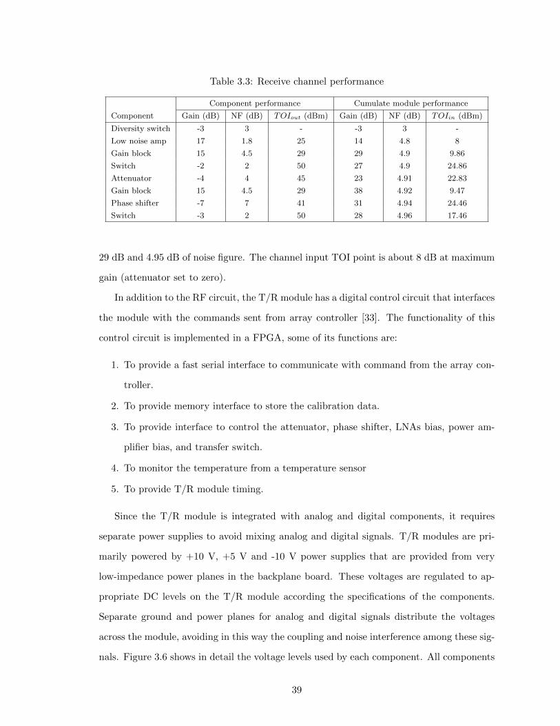
Table 3.3: Receive channel performance
Component performance Cumulate module performance
Component Gain (dB) NF (dB) TOIout (dBm) Gain (dB) NF (dB) TOIin (dBm)
Diversity switch -3 3 - -3 3 -
Low noise amp 17 1.8 25 14 4.8 8
Gain block 15 4.5 29 29 4.9 9.86
Switch -2 2 50 27 4.9 24.86
Attenuator -4 4 45 23 4.91 22.83
Gain block 15 4.5 29 38 4.92 9.47
Phase shifter -7 7 41 31 4.94 24.46
Switch -3 2 50 28 4.96 17.46
29 dB and 4.95 dB of noise figure. The channel input TOI point is about 8 dB at maximum
gain (attenuator set to zero).
In addition to the RF circuit, the T/R module has a digital control circuit that interfaces
the module with the commands sent from array controller [33]. The functionality of this
control circuit is implemented in a FPGA, some of its functions are:
1. To provide a fast serial interface to communicate with command from the array con-
troller.
2. To provide memory interface to store the calibration data.
3. To provide interface to control the attenuator, phase shifter, LNAs bias, power am-
plifier bias, and transfer switch.
4. To monitor the temperature from a temperature sensor
5. To provide T/R module timing.
Since the T/R module is integrated with analog and digital components, it requires
separate power supplies to avoid mixing analog and digital signals. T/R modules are pri-
marily powered by +10 V, +5 V and -10 V power supplies that are provided from very
low-impedance power planes in the backplane board. These voltages are regulated to ap-
propriate DC levels on the T/R module according the specifications of the components.
Separate ground and power planes for analog and digital signals distribute the voltages
across the module, avoiding in this way the coupling and noise interference among these sig-
nals. Figure 3.6 shows in detail the voltage levels used by each component. All components
39

are directly connected to the power planes, except the amplifiers used in the transmitter
and receiver blocks. The drain bias voltages for these amplifiers are driven by load switches,
which in turns are controlled by the T/R signal generated by a digital controller.
3.4.2 Diversity Switch Design
Early on in the design of the T/R module, it became apparent that PIN diodes were the
most appropriated switching element available. GaAs (Gallium Arsenide) MMIC switches
that could drive 2 W were not commercially available. For that reason, a large signal GaAs
Pin diode diversity switch is proposed. The switch uses a star configuration of 4 Single-Pole
Single-Throw (SPST) switches [44]. A characteristic of microwave SPST switches is that
diodes are spaced by quarter-wavelength transmissions, which help to increase the isolation
when multiplex diodes are used.
Each pole is independently controlled by a bipolar control signal, as illustrated in Figure
3.7a. The entire switch incorporates a total of 10 GaAs PIN diodes: two diodes at each arm
to increase the isolation between ports, and an additional diode in the polarization switches
to terminate the ports in a load of 50 Ω when they are switched off. Matched loads are
needed in the ports to terminate the radiating array element at its characteristic impedance
during the antenna calibration. The bias networks were designed with two radial microstrip
radial stub and high impedance microstrip lines, see Figure 3.7b.
An important aspect of the switch design is that its implementation differs from the
conventional approaches because the diode cathodes are not directly connected to grounded
vias. When diodes are directly grounded with vias, the insertion loss of the switch tends to
increase by the impedance of the vias, especially at high frequencies. To avoid this problem,
the diode cathodes are directly connected to microstrip lines that are previously grounded
to zero potential. To keep a low insertion loss, the reactance of equivalent impedance seen
from diode anodes is cancelled out by using microstrip radial stubs, which are also part of
the bias networks. Designing these networks is the most critical part of the switch.
The switch was designed, optimized and simulated in a 2D electromagnetic simulator.
The optimization focused in the tuning of the microstrip radial stubs that cancel out the
diode reactance. An empirical model of the PIN diode in the simulator was used. To reduce
40
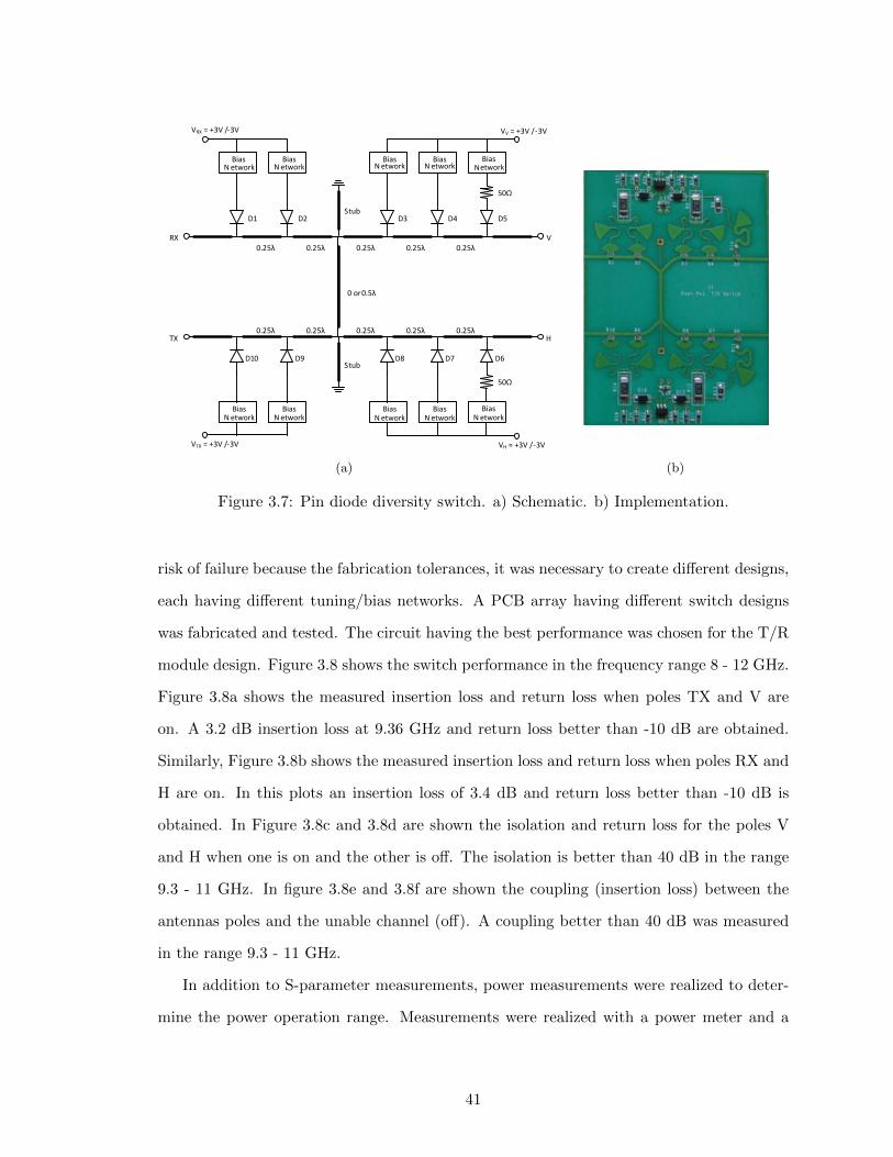
VH = +3V / -3V
Bias N etwork
Bias N etwork
Bias N etwork
Bias N etwork
Bias N etwork
Bias N etwork
Bias N etwork
Bias N etwork
Bias Network
Bias N etwork
D1 D2 D3 D4 D5
D10 D9 D8 D7 D6
50Ω
50Ω
RX
V
H
TX
0.25λ 0.25λ 0.25λ 0.25λ 0.25λ
0.25λ 0.25λ 0.25λ 0.25λ 0.25λ
0 or 0.5λ
Stub
Stub
VTX = +3V / -3V
VV = +3V / -3V VRX = +3V / -3V
(a) (b)
Figure 3.7: Pin diode diversity switch. a) Schematic. b) Implementation.
risk of failure because the fabrication tolerances, it was necessary to create different designs,
each having different tuning/bias networks. A PCB array having different switch designs
was fabricated and tested. The circuit having the best performance was chosen for the T/R
module design. Figure 3.8 shows the switch performance in the frequency range 8 - 12 GHz.
Figure 3.8a shows the measured insertion loss and return loss when poles TX and V are
on. A 3.2 dB insertion loss at 9.36 GHz and return loss better than -10 dB are obtained.
Similarly, Figure 3.8b shows the measured insertion loss and return loss when poles RX and
H are on. In this plots an insertion loss of 3.4 dB and return loss better than -10 dB is
obtained. In Figure 3.8c and 3.8d are shown the isolation and return loss for the poles V
and H when one is on and the other is off. The isolation is better than 40 dB in the range
9.3 - 11 GHz. In figure 3.8e and 3.8f are shown the coupling (insertion loss) between the
antennas poles and the unable channel (off). A coupling better than 40 dB was measured
in the range 9.3 - 11 GHz.
In addition to S-parameter measurements, power measurements were realized to deter-
mine the power operation range. Measurements were realized with a power meter and a
41
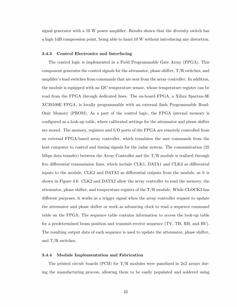
signal generator with a 10 W power amplifier. Results shown that the diversity switch has
a high 1dB compression point, being able to hand 10 W without introducing any distortion.
3.4.3 Control Electronics and Interfacing
The control logic is implemented in a Field Programmable Gate Array (FPGA). This
component generates the control signals for the attenuator, phase shifter, T/R switches, and
amplifier’s load switches from commands that are sent from the array controller. In addition,
the module is equipped with an I2C temperature sensor, whose temperature register can be
read from the FPGA through dedicated lines. The on-board FPGA, a Xilinx Spartan-3E
XC3S100E FPGA, is locally programmable with an external flash Programmable Read-
Only Memory (PROM). As a part of the control logic, the FPGA internal memory is
configured as a look-up table, where calibrated settings for the attenuator and phase shifter
are stored. The memory, registers and I/O ports of the FPGA are remotely controlled from
an external FPGA-based array controller, which translates the user commands from the
host computer to control and timing signals for the radar system. The communication (25
Mbps data transfer) between the Array Controller and the T/R module is realized through
five differential transmission lines, which include CLK1, DATA1 and CLK3 as differential
inputs to the module, CLK2 and DATA2 as differential outputs from the module, as it is
shown in Figure 3.6. CLK2 and DATA2 allow the array controller to read the memory, the
attenuator, phase shifter, and temperature register of the T/R module. While CLOCK3 has
different purposes, it works as a trigger signal when the array controller request to update
the attenuator and phase shifter or work as advancing clock to read a sequence command
table on the FPGA. The sequence table contains information to access the look-up table
for a predetermined beam position and transmit-receive sequence (TV, TH, RH, and RV).
The resulting output data of each sequence is used to update the attenuator, phase shifter,
and T/R switches.
3.4.4 Module Implementation and Fabrication
The printed circuit boards (PCB) for T/R modules were panelized in 2x2 arrays dur-
ing the manufacturing process, allowing them to be easily populated and soldered using
42

8 8.5 9 9.5 10 10.5 11 11.5 12−30
−25
−20
−15
−10
−5
0TX(ON), V(ON)
frequency (GHz)
Am
plitu
de (
dB)
RL(TX)IL(TX,V)RL(V)
(a)
8 8.5 9 9.5 10 10.5 11 11.5 12−30
−25
−20
−15
−10
−5
0RX(ON), H(ON)
frequency (GHz)
Am
plitu
de (
dB)
RL(RX)IL(RX,V)RL(H)
(b)
8 8.5 9 9.5 10 10.5 11 11.5 12−60
−50
−40
−30
−20
−10
0V(ON), H(OFF)
frequency (GHz)
Am
plitu
de (
dB)
RL(V)IS(V,H)RL(H)
(c)
8 8.5 9 9.5 10 10.5 11 11.5 12−60
−50
−40
−30
−20
−10
0V(OFF), H(ON)
frequency (GHz)
Am
plitu
de (
dB)
RL(V)IS(V,H)RL(H)
(d)
8 8.5 9 9.5 10 10.5 11 11.5 12−60
−50
−40
−30
−20
−10
0RX(OFF), V(ON)
frequency (GHz)
Am
plitu
de (
dB)
RL(RX)IL(RX,V)RL(V)
(e)
8 8.5 9 9.5 10 10.5 11 11.5 12−60
−50
−40
−30
−20
−10
0TX(OFF), H(ON)
frequency (GHz)
Am
plitu
de (
dB)
RL(TX)IL(TX,V)RL(H)
(f)
Figure 3.8: Diversity switch performance as a function of frequency.
43

standard processes. In addition, arrayed PCBs can help to reduce cost because they fewer
fabrication steps which speeds the assembly. A picture of a fully populated T/R module
is shown in Figure 3.9. The PCB comprises six circuit layers fabricated on a hybrid con-
struction of Rogers 4350 and FR4, see Figure 3.10 . A laminate of 10 mil Rogers 4350 in
the TOP layer is used to implement the RF and digital sections. The remaining layers,
four FR4 laminates including the bonding adhesives, are used to implement the analog and
digital ground/power planes, and to distribute the control signals. The PCB is designed to
have low thermal impedance from the power amplifier footprint through the board mount-
ing plate, which works as a heat spreader. A thermal patch isolates the PCB from the
baseplate avoiding that vias and transmission lines be short-circuited.
In Figure 3.9, the RF components are COTS plastic-packaged GaAs microwave mono-
lithic integrated circuits (MMICs). The large square containing microstrip lines and radial
stubs to the right of the module is the high power diversity switch. The area inside the
gold square to the left of the module corresponds to the digital components and interfacing
section. The two ports at the right side of the module are SMP sub-miniature connectors
that connect to the radiating element via short coaxial cables. The two ports at the left
side are SMA connectors that connect the TR module to two separate RF manifolds. All
components except the connectors were placed on the board using pick and place machine.
The module with enclosure weights 140 g and has a dimension of 6.6 cm x 11.2 cm.
3.4.5 Measurements
One of the challenges of producing phased-array antennas is the large number of T/R
modules that must be tested during the development phase or prototype production. In
addition, the testing of a single module is a labor intensive that generally involves hundreds
or thousands of measurements under different conditions. The use of automated equipment
is a requirement to reduce cost and time while keeping a standardized process. Based on
this need, an automated test station was specifically designed for this project. The test
station is based on a PNA series Network Analyzer from Agilent that is remotely controlled
via LAN (local area network) from a host computer. Figure 3.11 shows the schematic
diagram of the measurement equipment setup for the T/R module evaluation. The entire
44

Figure 3.9: Photograph of the implemented T/R Module.
½ oz. Cu
Roger 4350, 0010"
½ oz. Cu
FR4 Prepreg 7628 0.014"± 0.002”
½ oz. Cu
FR4 0.010"± 0.002”
½ oz. Cu
FR4 Prepreg 7628 0.014"± 0.002”
½ oz. Cu
FR4 0.010"± 0.002”
½ oz. Cu
Layer 1, TOP
Layer 2, AGND
Layer 3, APWR
Layer 4, DPWR
La yer 5, DGD
Layer 6, BOTTOM
0.062”±0.004”
Figure 3.10: PCB cross section.
45
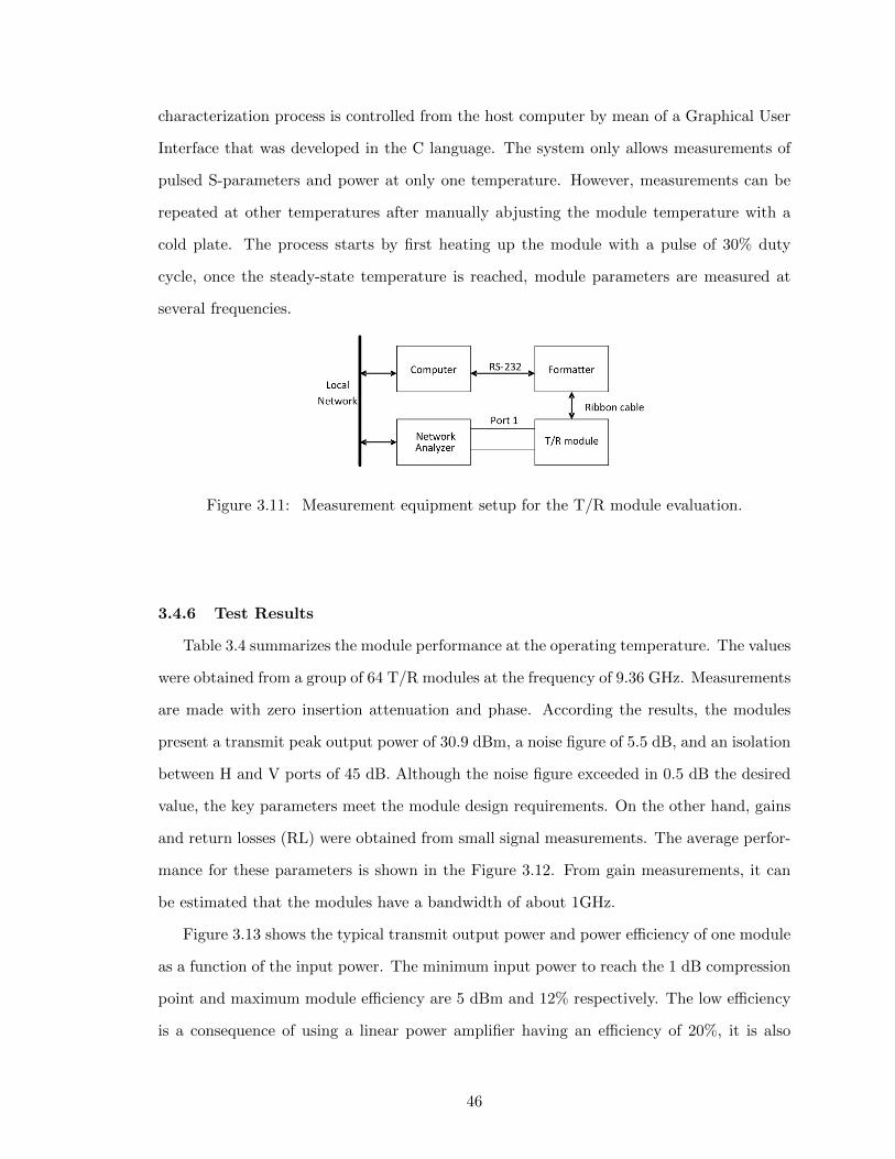
characterization process is controlled from the host computer by mean of a Graphical User
Interface that was developed in the C language. The system only allows measurements of
pulsed S-parameters and power at only one temperature. However, measurements can be
repeated at other temperatures after manually abjusting the module temperature with a
cold plate. The process starts by first heating up the module with a pulse of 30% duty
cycle, once the steady-state temperature is reached, module parameters are measured at
several frequencies.
Figure 3.11: Measurement equipment setup for the T/R module evaluation.
3.4.6 Test Results
Table 3.4 summarizes the module performance at the operating temperature. The values
were obtained from a group of 64 T/R modules at the frequency of 9.36 GHz. Measurements
are made with zero insertion attenuation and phase. According the results, the modules
present a transmit peak output power of 30.9 dBm, a noise figure of 5.5 dB, and an isolation
between H and V ports of 45 dB. Although the noise figure exceeded in 0.5 dB the desired
value, the key parameters meet the module design requirements. On the other hand, gains
and return losses (RL) were obtained from small signal measurements. The average perfor-
mance for these parameters is shown in the Figure 3.12. From gain measurements, it can
be estimated that the modules have a bandwidth of about 1GHz.
Figure 3.13 shows the typical transmit output power and power efficiency of one module
as a function of the input power. The minimum input power to reach the 1 dB compression
point and maximum module efficiency are 5 dBm and 12% respectively. The low efficiency
is a consequence of using a linear power amplifier having an efficiency of 20%, it is also
46

Table 3.4: T/R module performance summary at 9.36GHz.
Parameter H-Pol V-Pol
Transmit gain (dB) 24.5 24.7
Transmit peak power (dBm) 30.9 30.8
Transmit input 1 dB compression (dBm) 5 5
Transmit input return loss (dB) -15.5 -15.6
Tx small signal gain variation over temperature (dB/oC) 0.09 0.09
Receive gain (dB) 27.3 27.1
Receive input 1dB compression -15.7 -15.2
Minimum noise Floor (dB) 5.4 5.6
Receive input return loss (dB) -12.7 -11.8
Receive output return loss (dB) -12.9 -13
Rx gain variation over temperature (dB/oC) 0.016 0.016
Isolation between RFin and RFout ports (dB) 78 78
Isolation between V and H port (dB) 47.4 46
Phase shifter step (degrees) 5.531 5.531
RMS phase error (degrees) 1.49 1.49
Attenuator step (dB) 0.476 0.476
RMS attenuation error (dB) 0.161 0.161
Transmit and receive settling time (µsec) <2 <2
Overall module efficiency 12% 12%
8 8.2 8.4 8.6 8.8 9 9.2 9.4 9.6 9.8 10-30
-20
-10
0
10
20
30
Frequency (Ghz)
Magnitude (
dB
)
Rx-V GainRx-H GainTx-V GainTx-H GainRx RLTx RLH RLV RL
Figure 3.12: Average gain and return losses for 64 modules.
47
−20 −15 −10 −5 0 5 100
5
10
15
20
25
30
35
Input Power (dBm)
Out
put P
ower
(dB
m)
−20 −15 −10 −5 0 5 100
10
20
TX
Effi
cien
cy (
%)
Figure 3.13: Transmit peak output power and module efficiency versus input power.
because insertion loss produced by the diversity switch and low efficiency of DC linear
voltage regulators.
The small signal gain/phase and Tx saturation power performance are shown in Figure
3.14 as a function of temperature. Measurements are normalized to the operating temper-
ature of 32 oC. The gain and phase in the Rx channel decay at a rate of 0.016 dB/oC and
0.6 deg/oC respectively. The results show that these variations can be compensated with
one attenuation step and 3 phase shifting steps in the temperature range. In contracts, the
gain in the Tx channel decay a faster rate, 0.09 dB/oC, with a similar phase variation, 0.6
deg/oC. For large signal excitation, the relative saturation power (loss) increases at a rate
of 0.018 dB/oC.
The typical gain and phase performance versus the attenuator and phase shifter states
of one receive module at 9.36 GHz are shown in Figure 4.4 (Chapter 4). The plots comprise
of a set of 64 curves, each representing the response at a specific attenuation state. The
results show that the gain is affected by the insertion loss of each phase shifter state. Similar
effect is observed in the phase, but its value is only affected by the insertion phase of the
attenuator. For example, at zero phase state, the module phase varies from 0o to -50o when
48

30 35 40 45 50 55 60 65−4
−3
−2
−1
0
Module Temperature (°C)
Rel
ativ
e M
agni
tude
30 35 40 45 50 55 60 65−20
−15
−10
−5
0
RX
Pha
se (
deg)
Rx small signal Gain (dB)Tx small signal Gain (dB)Tx sat. Power Loss(dBm)
Rx small signal PhaseTx small signal Phase
Figure 3.14: Relative gain/phase performance and saturation power loss versus moduletemperature.
the attenuator is adjusted from zero to maximum attenuation. This effect can be corrected
by using calibration techniques and by storing the corrected settings in the module memory.
Ultimatly the calibration should be done for different temperatures. Results could be used,
for instance, to compensate the gain/phase deviation due to the temperature, as it is shown
in Figure 3.14. On the other hand, the step size (resolution) for the attenuator and phase
shifter as a function of component state for a typical T/R module is shown in Figure 3.15.
The attenuator presents a non-uniform attenuation step versus states; the mean step and
standard deviation are 0.457 dB and 0.161 dB, respectively. Similar behavior is obtained
with the phase shifter, which has a mean phase step of 5.54o and standard deviation of
1.49o.
Measurements were also performed in the time domain to determine the settling time
of T/R modules. Settling time is the time required for the output to reach the steady-
state within a given error bound following some input stimulus. For this test, a signal
generator connected to module input and a microwave Schottky diode detector connected
to the module output were used. The diode voltage was measured with a high-speed digital
oscilloscope. Figure 3.16a shows the typical switching characteristic of a T/R module for a
49

0 20 40 600
0.1
0.2
0.3
0.4
0.5
0.6
0.7
0.8
0.9
1
Atte
nuat
ion
step
(n)
= S
21dB
(n,0
) −
S21
dB(n
−1,
0) (
dB)
Attenuation index, n
mean = 0.457 dB, std = 0.161 dB
0 20 40 600
1
2
3
4
5
6
7
8
9
10
Pha
se s
tep(
n) =
pha
se(S
21(n
,0))
− p
hase
(S21
dB(n
−1,
0))
(deg
)
phase index, n
mean = 5.54 deg, std = 1.49 deg
Figure 3.15: Resolution step as a function of component states. Left: Attenuator. Right:Phase shifter
pulse of 100 µsec. The green signal represents the control signal applied to either transmit
channel or receive channels and yellow signal is the IF signal measured at the channel
output. The voltage demodulated by the diode detector during rise time for both transmit
and receive channel are shows in figure 3.16b and 3.16c, respectively. The settling time in
both cases is about 2 µsec. This values is important because it can indicate the maximum
PRF that can be implemented by the radar. For example, assuming the minimum pulse
width of the radar is τpw= 1 µsec and maximum duty cycle is limited at DC= 30% to protect
the T/R module power amplifier of excessive heating. It is obvious that the waveform must
be transmitted until the settling time has elapsed to avoid the amplitude modulation that
could created by the variable gain. Therefore, the transmit channel will be enable by the
time τst+ τpw= 2µsec+1 µsec= 3 µsec. The minimum pulse repetition interval is obtained
as
PRI =τst + τpwDC
=2µS + 1µS
0.3= 10µS
using this value one can find the maximum PRF is 1/PRI = 100 kHz. The wide PRF-range
enable the system to work in a widely range of radar applications including weather and
50

(a)
(b) (c)
Figure 3.16: Typical switching characteristics of a T/R module.a) RF and DC bias pulse.b) RF pulse at the transmitter output. c) RF pulse at the receiver output.
airborne surveillance. On the other hand, Figure 3.16c suggests the radar gain in receive
must be calibrated during the settling time to observe targets close to the radar.
3.5 Backplane Board
3.5.1 Description
The backplane is the interface between TR modules and other radar subsystems. All RF
signal distribution lines, DC bias signal, and digital bus that connect the T/R modules with
the transceiver, power supplies, and array Controller are located in this board. The array
system uses four backplanes to interface the 64 T/R modules with other radar subsystems.
Figure 3.17 depicts how the radar subsystems are interconnected through the backplane and
what sections are integrated in it. The RF, digital and DC bias sections are implemented in
51

RF power distribution
network
Dc power
distribution network
Backplane bus
Array Controller
DC to DC converters
Transceiver
T/R module Array element
Backplane
Figure 3.17: Backplane subsystem.
FR4 Prepreg 7628
0.010"± 0.002”
½ oz. Cu
Roger 4350, 0. 010"
½ oz. Cu
0.010"± 0.002”
2 oz. Cu
0.010"± 0.002” 2 oz. Cu FR4 Prepreg 7628
0.010"± 0.002”
0.010"± 0.002”
1 oz. Cu FR4
0.010"± 0.002”
0.010"± 0.002” 1 oz. Cu
Layer 1, RF signal, DC signal
Layer 2, A nalog ground
Layer 3, Digital ground
Layer 4, DC signal (+10 Va, - 10Va)
Layer 5, DC signal (+7Vd)
Layer 6, A nalog ground
0.062 ”±0.006” FR4
0.010"± 0.002”
Figure 3.18: Backplane PCB cross section.
a multilayer hybrid PCB fabricated on FR4 and Roger 4350 material. Figure 3.18 shows the
board layout structure and the layers assigned to each subsystem. Each section is complete
isolated each other by ground planes. The RF and DC power distribution networks partially
share the top layer because both the RF connectors and DC bias connectors are assembled
on it. The cost model for the backplane is described in Appendix B.
Figure 3.19 shows the front and rear view of the backplane and how the beamformer
structure is assembled. In Figure 3.19a, the from view shows the backplane’s top layer
where the RF manifold are designed. The rear view shows the header connector array that
forms the backplane bus. In Figure 3.19b, the T/R module header connector is plugged to
backplane bus, while the RF connectors are connected to RF manifold with RF semi-rigid
cables. Note that the corporate feeds are enclosed in a metallic lid in order to eliminate any
radiation or coupling with other subsystems. The whole RF power distribution network is
52

shown in Figure 3.20. Two 1:4 power dividers are needed to connect the outputs from the
4 power combiners and inputs of the 4 power dividers, respectively.
3.5.2 Corporate Feed Network
3.5.2.1 Design and Implementation
Typical components used in the design of corporate feeds are the microstrip T-junction,
Wilkinson power divider, and rat-race coupler [18]. T-junctions and Wilkinson power di-
vider are three-port networks that can split the power equally. T-junctions are passive
components of simple design that are characterized by a poor performance. Wilkinson
power dividers are also simple components which solve the matching and poor isolation
problem of T-junctions. The drawback of these two components is that both are lossy
components. On the other hand, rat-race couplers (also known as hybrid ring coupler) are
lossless four-port networks that provide ports with very good return loss and high isolation.
Compared with thee-port networks, the rat-race couplers are larger structures, but they
provide a better performance. Based on the system requirements, such as low insertion loss
and high isolation, the rat-race coupler was chosen for this design.
A rat-race coupler consists a 3λ0/2 ring of microstrip line with line impedance of 70.71
Ω an 4 microstrip lines of 50 Ω spaced at intervals of λ0/4 as shown in Figure 3.21a. The
input power at port 1 splits and travels both ways round the ring. At ports 2 and 3 the
signal arrives in phase and adds whereas at port 4 it is out of phase and cancel. Ports 2
and 3 are in phase with each other, while port 4 is terminated in a resistive load of 50 Ω. A
1:16 corporate feed is designed by connecting several rat-race couplers in cascade at ports
2 and 3 as is shown in Figure 3.21b. Fifteen couplers are needed in total. Note that 50
Ohms terminations at port 4 of each coupler are grounded by radial stubs and that half of
the corporate feed is symmetrically opposite to the other half. Theoretically, the insertion
loss in a 1:16 power divider is 10log10(1/16)=-12 dB.
The corporate feed is implemented in a 10 mil Roger 4350 material, its design was
simulated in 2D electromagnetic simulator. Simulated results indicated a good amplitude
and phase balance among output ports. A photography of the fabricated 1:16 corporate
feed network is shown in Figure 3.22. The ports are connected to surface mount SMA
53

(a)
(b)
Figure 3.19: Backplane board and Beamformer structure. a) Front and rear view of back-plane board. b) Beamformer assembly
54

Figure 3.20: RF power distribution network.
λ/4
λ/4
λ/4
3λ/4
Zo
Zo Zo
Zo
√2Zo
P1
P2
P3
P4
(a)
(b)
Figure 3.21: Component and schematic circuit of the RF power distribution network. a)Rat-race coupler. b) 1:16 corporate feed.
55

Figure 3.22: Corporate feed layout.
connectors, and the peripheral is surrounded by a gold-color ground plane that allows the
attachment of a conducting lid that can be placed over the PCB to provide isolation.
3.5.2.2 Results
Measurements were made using a two port vector network analyzer in the frequency
range from 9.06 GHz to 9.66 GHz. Each output port was measured while the other ports
were terminated in 50 Ohms loads. The return loss for each of the 17 ports is depicted in
Figure 3.23. In average, the return loss is lower than -10 dB. The amplitude and phase
insertion loss for each of the 16 branches is depicted in Figure 3.24. In Figure 3.24a, the
insertion loss is -16.6 dB at 9.36 Ghz and there is approximately 0.3 dB spread in insertion
loss among output ports. A increment of 4.6 dB with respect to theoretical insertion loss was
obtained. This value is attributed to losses in the transmission lines and SMA connectors.
In figure 3.24b, there is approximately a 7o spread in the insertion phase.
3.5.3 Backplane Bus
3.5.3.1 Design
Backplanes have been widely used in high-speed communication and computer system
because they are low cost and reliable system. However, their use in phased array antennas
has been unknown or it has not been reported. A backplane is an interconnect system that
allows the parallel connection of various digital cards (PCBs) to a shared bus. They should
be designed properly to guarantee signal integrity and high-speed performance. To meet
these high performance standards, the buses use differential signaling over a pair of mi-
56
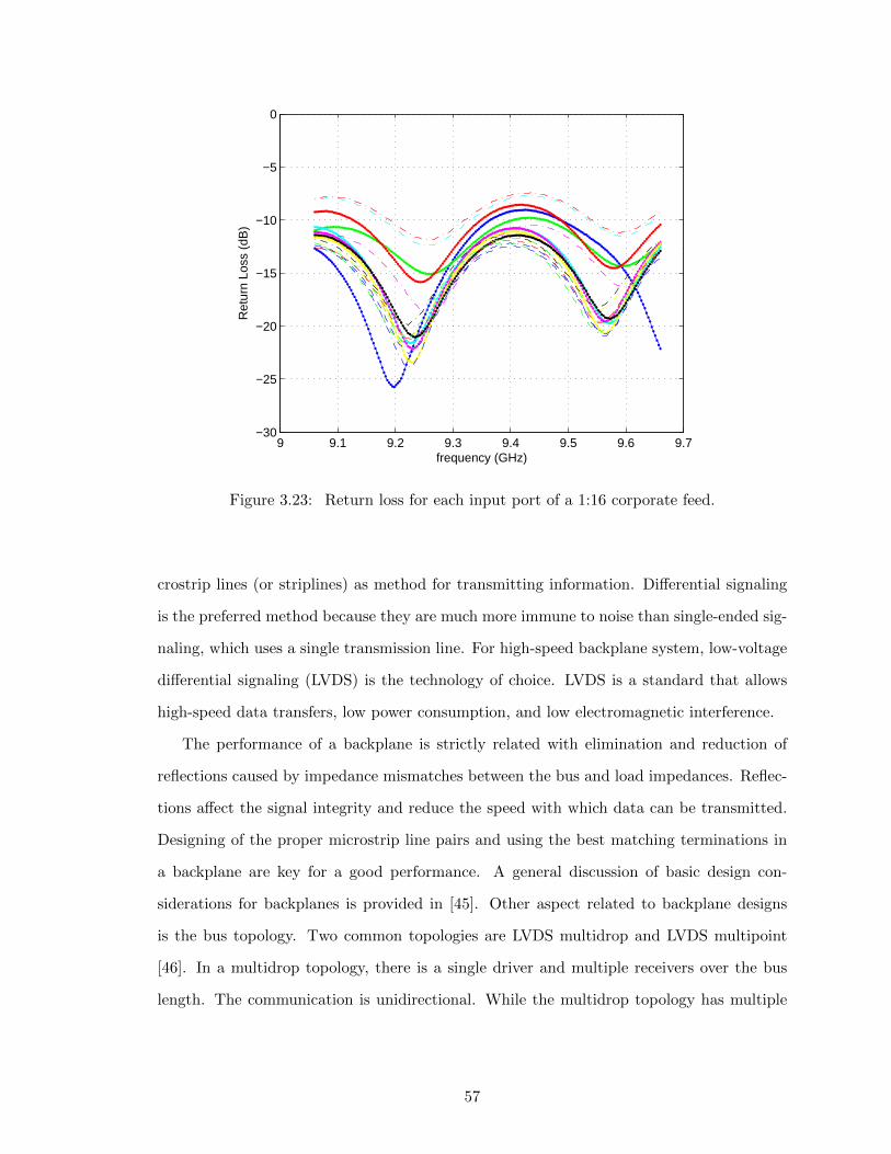
9 9.1 9.2 9.3 9.4 9.5 9.6 9.7−30
−25
−20
−15
−10
−5
0
frequency (GHz)
Ret
urn
Loss
(dB
)
Figure 3.23: Return loss for each input port of a 1:16 corporate feed.
crostrip lines (or striplines) as method for transmitting information. Differential signaling
is the preferred method because they are much more immune to noise than single-ended sig-
naling, which uses a single transmission line. For high-speed backplane system, low-voltage
differential signaling (LVDS) is the technology of choice. LVDS is a standard that allows
high-speed data transfers, low power consumption, and low electromagnetic interference.
The performance of a backplane is strictly related with elimination and reduction of
reflections caused by impedance mismatches between the bus and load impedances. Reflec-
tions affect the signal integrity and reduce the speed with which data can be transmitted.
Designing of the proper microstrip line pairs and using the best matching terminations in
a backplane are key for a good performance. A general discussion of basic design con-
siderations for backplanes is provided in [45]. Other aspect related to backplane designs
is the bus topology. Two common topologies are LVDS multidrop and LVDS multipoint
[46]. In a multidrop topology, there is a single driver and multiple receivers over the bus
length. The communication is unidirectional. While the multidrop topology has multiple
57

9 9.1 9.2 9.3 9.4 9.5 9.6 9.7−20
−19
−18
−17
−16
−15
−14
−13
−12
−11
−10
frequency (GHz)
Inse
rtio
n Lo
ss (
dB)
(a)
9 9.1 9.2 9.3 9.4 9.5 9.6 9.7−200
−150
−100
−50
0
50
100
150
200
frequency (GHz)
Inse
rtio
n P
hase
(de
g)
(b)
Figure 3.24: Insertion loss and insertion phase measured at each branch of a 1:16 corporatefeed. a) Insertion loss. b) Insertion phase.
58

signal drivers and receivers, all sharing a single bus. This configuration allows bidirectional
communications.
For simplicity, in this project, a multi-drop topology for the communication and beam-
steering control system was chosen. The backplane bus that connects the array controller
with T/R modules uses five transmission line pairs (buses). Three buses are used to transmit
data (ones bus) and clocks (two buses) from the array controller to T/R modules; each of
these buses can be represented as shown in the top in Figure 3.25. There also two buses to
transmit data and clock from the T/R modules to array controller. In this case, each bus can
be represented as shown in the lower part in Figure 3.25; where each driver is a tree-states
transmitter. Normally all driver outputs are set to high impedance and only the driver that
responds to array controller commands can transmit over the bus. A general diagram of
the bus topology used in the array system is depicted in Figure 3.26. The configuration
used two arms, each having two backplanes in cascade with 32 T/R modules connected in
parallel. Two repeater/buffer boards connected at the end of each arm are used to extend
the connection between the beamformer structure and the array controller. Ultimately, the
three buses transfering data and clock toward T/R modules are connected in parallel in
the array controller. While the two buses coming from T/R modules are multiplexed into
a single data line. The advantage of this topology is that all T/R modules are connected
in parallel at the Array controller using a simple, high speed, and low cost communication
bus.
D
R RRRRRR
R
D DDDDDD
RL
RL
Figure 3.25: Multidrop topology.
59
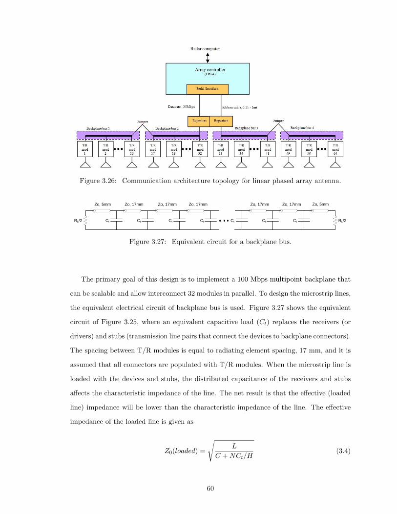
Figure 3.26: Communication architecture topology for linear phased array antenna.
Zo, 17mm Zo, 17mm Zo, 17mm Zo, 17mm Zo, 5mmZo, 17mmZo, 5mm
Ct Ct Ct Ct Ct CtCtRL/2 RL/2
Figure 3.27: Equivalent circuit for a backplane bus.
The primary goal of this design is to implement a 100 Mbps multipoint backplane that
can be scalable and allow interconnect 32 modules in parallel. To design the microstrip lines,
the equivalent electrical circuit of backplane bus is used. Figure 3.27 shows the equivalent
circuit of Figure 3.25, where an equivalent capacitive load (Ct) replaces the receivers (or
drivers) and stubs (transmission line pairs that connect the devices to backplane connectors).
The spacing between T/R modules is equal to radiating element spacing, 17 mm, and it is
assumed that all connectors are populated with T/R modules. When the microstrip line is
loaded with the devices and stubs, the distributed capacitance of the receivers and stubs
affects the characteristic impedance of the line. The net result is that the effective (loaded
line) impedance will be lower than the characteristic impedance of the line. The effective
impedance of the loaded line is given as
Z0(loaded) =
√L
C +NCt/H(3.4)
60
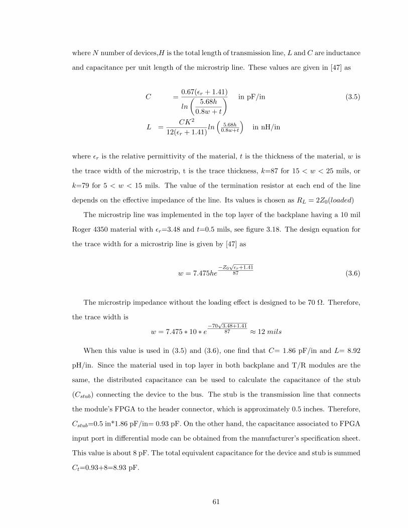
whereN number of devices,H is the total length of transmission line, L and C are inductance
and capacitance per unit length of the microstrip line. These values are given in [47] as
C =0.67(εr + 1.41)
ln
(5.68h
0.8w + t
) in pF/in (3.5)
L =CK2
12(εr + 1.41)ln(
5.68h0.8w+t
)in nH/in
where εr is the relative permittivity of the material, t is the thickness of the material, w is
the trace width of the microstrip, t is the trace thickness, k=87 for 15 < w < 25 mils, or
k=79 for 5 < w < 15 mils. The value of the termination resistor at each end of the line
depends on the effective impedance of the line. Its values is chosen as RL = 2Z0(loaded)
The microstrip line was implemented in the top layer of the backplane having a 10 mil
Roger 4350 material with εr=3.48 and t=0.5 mils, see figure 3.18. The design equation for
the trace width for a microstrip line is given by [47] as
w = 7.475he−Z0√εr+1.4187 (3.6)
The microstrip impedance without the loading effect is designed to be 70 Ω. Therefore,
the trace width is
w = 7.475 ∗ 10 ∗ e−70√3.48+1.4187 ≈ 12 mils
When this value is used in (3.5) and (3.6), one find that C= 1.86 pF/in and L= 8.92
pH/in. Since the material used in top layer in both backplane and T/R modules are the
same, the distributed capacitance can be used to calculate the capacitance of the stub
(Cstub) connecting the device to the bus. The stub is the transmission line that connects
the module’s FPGA to the header connector, which is approximately 0.5 inches. Therefore,
Cstub=0.5 in*1.86 pF/in= 0.93 pF. On the other hand, the capacitance associated to FPGA
input port in differential mode can be obtained from the manufacturer’s specification sheet.
This value is about 8 pF. The total equivalent capacitance for the device and stub is summed
Ct=0.93+8=8.93 pF.
61

With all the connector filled (32 connector), the total length of the backplane is approx-
imately 32*1.7 cm/2.54 = 21.41 inches. The effective impedance of the loaded microstrip
line is obtained from (3.7) as
Z0(loaded) =
√8.92
1.86 + 32 ∗ 8.93/21.41= 24.22 Ω (3.7)
To reduce the reflections at the ends, the termination resistor should be close to the
effective differential impedance of backplane. That is RL = 2Z0(loaded) = 2 ∗ 24.22 =
48.44Ω. Finally, this values was rounded to 50 Ω. Also, as part of the design, PSPICE
simulations using the equivalent circuit of the backplane were performed. The purpose of
the simulation was to verify signal integrity at different speeds. Simulations indicated that
the backplane bus can work perfectly up 100 Mbps.
3.5.3.2 Implementation
Figure 3.28 shows a photograph of the front view of the backplane, the board face where
the buses are implemented. There are five microstrip line pairs with termination pads at
the ends. The two black connectors at the ends are used to connect either repeater boards
or jumper cables. While the connector for the T/R modules are installed in the rear side
plane. A photograph of a partially assembled beamformer structure is shown in Figure 3.29.
Figure 3.28: Backplane bus layout.
62

Figure 3.29: Assembled beamformer structure.
3.5.3.3 Measurements
Testing consisted of measuring waveforms on the buses of two fully loaded backplanes
connected in cascade with a short ribbon cable. The data were clocked over the backplane
at a frequency of 25 Mbps. Single and differential waveforms for the input receiver are
shown in Figure 3.30. Measurements were made at the termination resistor. The differen-
tial waveform (V ) was calculated by the oscilloscope from the non-inverting receiver input
waveform (V p) and inverting receiver input waveform (V n). The three waveform show a
little undershoot or overshoot and small load reflections. The differential waveform have
substantial noise margins with respect to the receiver thresholds of ±10 mV. An eye dia-
gram for the differential waveform is shown in Figure 3.31. The jitter is about 1 nsec while
the eye rise time and eye fall time are about 5 nsec.
63

Figure 3.30: Serial data transmission in a backplane at 25 Mbps.
3.6 Beam Steering Control System
3.6.1 Architecture
A phased array with 64 elements, each having a T/R module with 16 control signals (6
bit phase shifter, 6 bit digital attenuator, transmit signal, receive signal, H polarization, and
V polarization), require of 16x64= 1024 control signals to switch the beam. Because of the
large amount of wiring that must be supplied to all T/R modules, the only practical solution
to reduce cost and wiring complexity is to use serial communication. The serial transmission
of this amount of data in a short time would require a large bandwidth and the use of well
designed high-speed serial interfaces that might increase the system costs. Fortunately, the
bandwidth problem can be avoided if a distributed beam steering control system is used. In
this type of system, the beam steering computer broadcasts phase gradients (for azimuth
and elevation) to all T/R module digital controllers, which generate phase and amplitude
settings that are needed to implement the beam [40, 48, 30, 49, 31]. The phase setting is
computed from the phase gradient, the element position in the array, and phase correction
constant of that particular element. While the amplitude, it is obtained typically from a
look up table. An example of phase calculation from phase gradients in the T/R modules is
given in [49]. The calculation of a 6-bit phase setting is carried out using a FPGA. The time
taken to broadcast a 36 bit phase gradient over 10 Mbps network (3.6 µsec) and to compute
64

Figure 3.31: Eye diagram for bus LVDS backplane at 25 Mbps.
the phase (2.12 µsec) was about 5.7 µsec. The problems with this implementation are that
the phase calculation is performed every transmit and receive pulse, and the computational
cost in time to generate each beam might be too large for adaptive short range radars (using
alternate polarization and beam multiplexing technique), which require short pulses (i.e. 1
µsec)
Rather than attempting to compute the phase with a digital controller, the BSCS devel-
oped in this work uses calibrated look-up tables to translate beam commands into calibrated
phase and amplitude settings. The look-up tables are unique for each T/R modules. They
store the phase shifter and attenuator states for each scan angle at all operation modes.
The advantages of this technique are: 1) The time taken to translate the command into
calibrated settings is much lower than the time taken to compute the calibrated setting with
a processor, 2) Digital controllers are simpler to design. Figure 3.32 shows a block diagram
of the key logic modules developed for the BSCS. The system consists of a network of cus-
tom state machines (digital controllers) implemented in the T/R module FPGAs, instead
of microprocessor core. State machines have the advantage of responding immediately and
in parallel to a large number of timing signals. The system is totally synchronous because
a global clock controls all operations. T/R modules are controlled by means of 16-bits
65

Digital controller 2
Serial to
parallel
interface
Look up table
(beam list)
Port
register
(current beam)H,VT,R
PS[5:0]AT[5:0]Sequence table
(next beam)
Digital controller 1
Digital controller 64
Digital controller 63
Digital controller 3
Serial to
parallel
interface
Sequence table
(next beam)
Look up table
(beam list)
Port
register
(current beam)H,VT,R
PS[5:0]AT[5:0]
Array controller
Data
Clock
Serial to
parallel
interface
Sequence table
(next beam)
Look up table
(beam list)
Port
register
(current beam)H,VT,R
PS[5:0]AT[5:0]
Serial to
parallel
interface
Sequence table
(next beam)
Look up table
(beam list)
Port
register
(current beam)H,VT,R
PS[5:0]AT[5:0]
Serial to
parallel
interface
Sequence table
(next beam)
Look up table
(beam list)
Port
register
(current beam)H,VT,R
PS[5:0]AT[5:0]
TR
Figure 3.32: Block diagram of the key logic modules used in beam steering control system.
commands and by a TR signal (called “CLK3” signal in the T/R module). The digital
controller includes a serial to parallel interface that passes the received commands to a 16
line parallel bus in the FPGA. A programmable sequence table stores the next sequence of
beams that must be implemented by the array. A look-up table then translates the beam
commands to calibrated settings. A port register stores the settings for the current beam
and generates control signals to RF components (attenuator, phase shifter, T/R switches,
V/H switch, amplifiers). The beam switching and timing are controlled at the rising edge
(transition for low to high level) of the TR signal. This signal also serves as “advance
signal”, which allows the next beam command can be read from the sequence table.
66

In order to understand the concept of operation behind the BSCS, let’s consider a specific
example. Suppose that the radar system is performing dual polarization measurements
with the sequence TH, RH, TV, RV, TH, RV, TV, and RH. A timing diagram illustrating
this operation mode is shown in Figure 3.33. For the nth scan angle, the array controller
generates a serial stream by concatenating 8 beam commands. The beam command includes
a bit for array channel (TR), a bit for polarization (HV), and several bits to represent the
scan angle as an integer binary number (beamID). The relationship between beamID
and scan angle is explained in chapter 4 (see equation 4.19). The sequence table for this
operation mode is defined in Table 3.5. Four different beams or radiation patterns must
be implemented by the beamforming network: two transmit beams (TH and TV) and two
receive beams (RH and RV). The serial stream having the sequence table is broadcasted
from the array controller to all T/R modules during the dead time between two dwell
periods. Each digital controller accepts the commands and stores them in a 8 words (16-
bits) memory (sequence table). Once this operation is completed, the read pointer points to
the first location of the sequence table, reading the first beam command. The command bits
are supplied in parallel to the corresponding input terminals of the look-up table, which
translates the beam commands to calibrated settings. The output data returned by the
look-up table contains the setting for the next beam including the bits T, R, H, V, PS[5:0],
and AT[5:0]. These bits are described in Table 3.6. The data will be hold by the look-up
table until the rising edge on the TR signal, at which point the data is latched in the output
port. Simultaneously, the read pointer of the sequence table advances one position for each
rising edge on the TR signal, reading the next beam command. Therefore, the first pulse
on the TR signal allows the transmit beam b0 to be implemented, and the same time, it
allows the next calibration setting (receive beam b1) to be read from the lookup table, as
shown in Figure 3.33. When the second pulse on the TR signal arrives, the receive beam b1
is implemented and the next calibration settings is read. This procedure is repeated until
the last command in the sequence table is read (receive beam b1), at this point the read
pointer of the sequence table is returned to point to the first location on the sequence table,
starting a new loop. The loop will run indefinitely until the sequence table is updated with
a new beam sequence.
67

clock
data
TR
b0 b1 b2 b3 b0 b3 b2 b1
TH RH TV RV TH RV TV RH
b0 b1 b2 b3 b0 b3 b2 b1
TH RH TV RV TH RV TV RH
b0 b1 b2 b3 b3 b2 b1
TH RH TV RV RV TV RH
b0 b1 b2 b3 b0 b3 b2 b1
TH RH TV RV TH RV TV RH
Dwell
period
Scan angle n+1
T
R
H
V
phs[5:0]
att[5:0]
beam
mode
Scan angle n
Dead
time
Transmitted
waveform
H V
Figure 3.33: Timing diagram of representative command/response sequence.
The communication and control architecture of the beam steering control system has
been designed to operate with clock signals up to 100 MHz. However, the clock was fixed to
25 MHz to get a low bit error rate (BER) in the serial communication. At this clock speed,
the sequence table is transmitted in the order of 6 µsec. A short-range radar operating
in alternate polarization and using 3 kHz PRF with 30 pulses of integration per channel,
has a dwell time of 4x30/3000= 40 msec. For this radar, the dead time to update the
Table 3.5: Data structure of sequence table
Beam command
sequence TR HV Scan angle beam index
TH 1 1 beamID b0
RH 0 1 beamID b1
TV 1 0 beamID b2
RV 0 0 beamID b3
TH 1 1 beamID b0
RV 0 0 beamID b3
TV 1 0 beamID b2
RH 0 1 beamID b1
68

Table 3.6: Digital controller interface signals.
Port Width Type Signal Description
DATA1 2 input differential Serial data line input
CLK1 2 input differential Serial clock line input
DATA2 2 output differential Serial data line output
CLK2 2 output differential Serial clock line output
CLK3 2 input differential Serial TR line input (TR signal)
RST 1 input single Reset line input
T 1 output single Transmit channel enable
R 1 output single Receive channel enable
H 1 output single Horizontal polarization enable
V 1 output single Vertical polarization enable
PS 6 output single Phase shifter control bits
AT 6 output single Attenuator control bits
SDA 1 bidirectional single I2C serial data line
SCL 1 output single I2C serial clock line
sequence table is about 6/40x103*100= 0.015% of the dwell period, which denotes a very
small fraction of time.
3.6.2 Interfacing Signals
The input and output signals used by the digital controller are defined in table 3.6. The
signals DATA1, CLK1, DATA2, CLK2, CLK3, and RST are supplied by the backplane bus
(see Figure 3.6). DATA1 and CLK1 are signals generated by the array controller. DATA2
and CLK2 are signals generated by the T/R modules when the array controller request
status information. The CLK3 signal (or TR signal) controls the beam switching in the
array and controls the signals generated by the output port. The RST signal is generated
by the array controlled, when it is set to 1, the state-machines and registers in all T/R
module are restarted.
The controller has an output port that generates the signals: T, R, H, V, PS, and AT .
These signals control the RF devices in the T/R module (see Figure 3.6)
3.6.3 Serial Communication
The communication system uses a serial data bus and a serial clock bus to transfers
data between the digital transmitters and receivers. The transmitter has a parallel-to-serial
interface that accepts 16-bit parallel data and then shifts it out bit by bit in an especial
69

d0 d1 d2 d3 d4 d5 d6 d7 d8 d9 d10 d11 d12 d13 d14 d15
start bitidle stop bit
Data
Clock
Figure 3.34: Transmission of a 16-bit word.
protocol. The data is transmitted with the least significant bit first. The receiver has a
serial-to-parallel interface that accepts serial data and then converts it to 16-bit parallel
data. There is one clock pulse for each data bit that is transmitted, see Figure 3.34. The
serial data bus is logically high when it is idle. The transmission starts with a start bit,
which is 0, followed serially by a 16-bit word, and ends with a stop bit, which is 1. At the
receiver, each bit is sampled on the middle of each bit period using the falling edge of the
clock signal. A transition on the serial data bus from idle to a low level is interpreted as
the beginning of communication.
3.6.4 Digital Command
T/R modules are controlled by means of commands that are based on 16-bit words.
There are two types of commands: broadcast and unicast. The broadcast commands con-
trol simultaneously all T/R modules using a common command, for example when a new
sequence table is loaded. On the contrary, the unicast commands are used to establish a di-
rect point-to-point communication between the array controller and a specific T/R module,
allowing the attributes of a particular module can be set or read. The digital controllers
accept four unicast commands: write port, write address register, write memory, and read
temperature register. The T/R module controller requires a 7-bit address to enable a read
or write operation. The first word in unicast, is the addressing commands, which comprises
a mandatory one in the most significant bit (this bit in 1 means a uncast communication),
followed by 6 reserved bits ( all bits are set in 1), a 6-bits module address (AD5-AD0),
a 2-bits register address (M1 and M0), and ends with a write/read select bit in the least
significant bit (refer to Table 3.7). The reserved bits can be used to extend the number
of T/R module addresses, allowing up to 4096 possible modules. The register address is
70
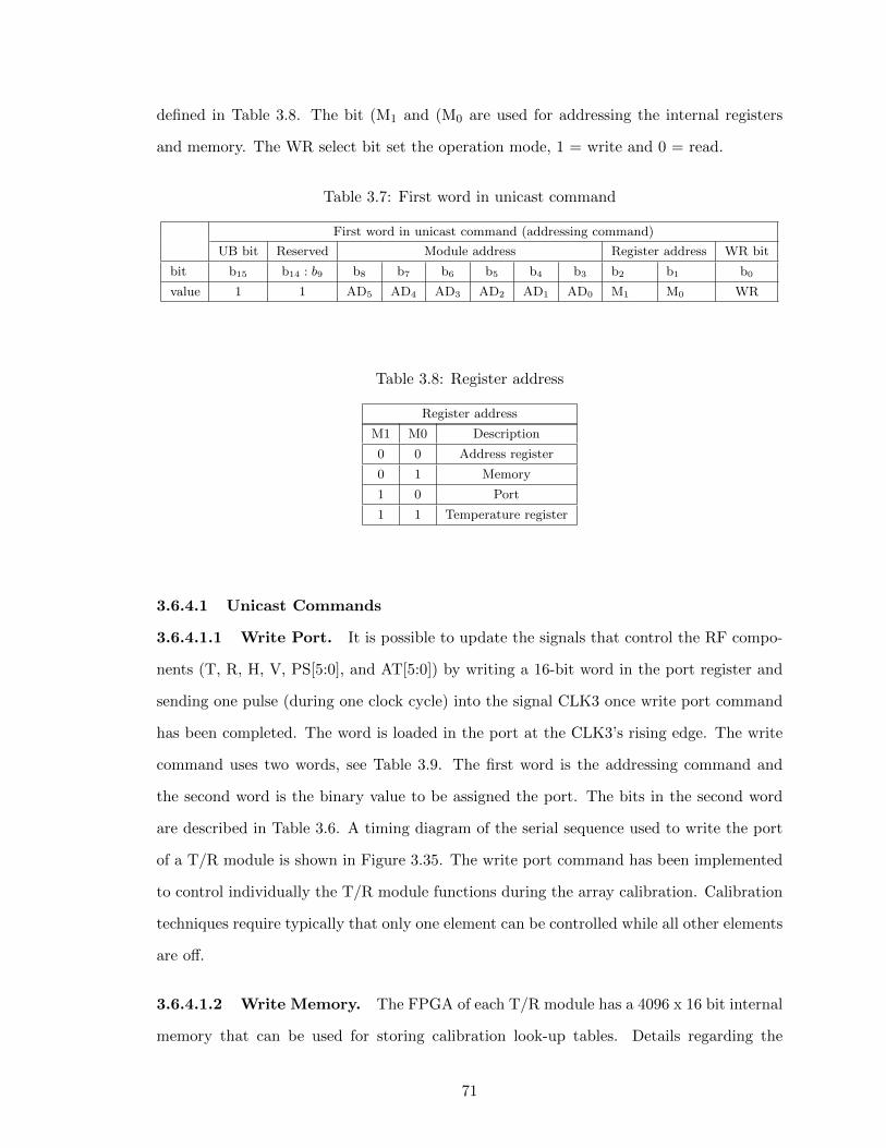
defined in Table 3.8. The bit (M1 and (M0 are used for addressing the internal registers
and memory. The WR select bit set the operation mode, 1 = write and 0 = read.
Table 3.7: First word in unicast command
First word in unicast command (addressing command)
UB bit Reserved Module address Register address WR bit
bit b15 b14 : b9 b8 b7 b6 b5 b4 b3 b2 b1 b0
value 1 1 AD5 AD4 AD3 AD2 AD1 AD0 M1 M0 WR
Table 3.8: Register address
Register address
M1 M0 Description
0 0 Address register
0 1 Memory
1 0 Port
1 1 Temperature register
3.6.4.1 Unicast Commands
3.6.4.1.1 Write Port. It is possible to update the signals that control the RF compo-
nents (T, R, H, V, PS[5:0], and AT[5:0]) by writing a 16-bit word in the port register and
sending one pulse (during one clock cycle) into the signal CLK3 once write port command
has been completed. The word is loaded in the port at the CLK3’s rising edge. The write
command uses two words, see Table 3.9. The first word is the addressing command and
the second word is the binary value to be assigned the port. The bits in the second word
are described in Table 3.6. A timing diagram of the serial sequence used to write the port
of a T/R module is shown in Figure 3.35. The write port command has been implemented
to control individually the T/R module functions during the array calibration. Calibration
techniques require typically that only one element can be controlled while all other elements
are off.
3.6.4.1.2 Write Memory. The FPGA of each T/R module has a 4096 x 16 bit internal
memory that can be used for storing calibration look-up tables. Details regarding the
71

Table 3.9: Write Port Command.
bit b15 b14 b13 b12 b11 b10 b9 b8 b7 b6 b5 b4 b3 b2 b1 b0
1stword
1 1 1 1 1 1 1 A5 A4 A3 A2 A1 A0 1 0 1
2ndword
H V T R PS5 PS4 PS3 PS2 PS1 PS0 AT5 AT4 AT3 AT2 AT1 AT0
1 1 1 1 1 1 1 1 1Data1
CLK1
AD5 AD4 AD3 AD2 AD1 AD0
H V T R PS2 PS1 PS0 AT5 AT4 AT3PS5 PS4 PS3 AT2 AT1 AT0Data1
CLK1
CLK3
CLK3
First word sequence
Second word sequence
Figure 3.35: Transmission of write port command.
look-up table organization are given in chapter 4. The memory write operation requires
an addressing command, followed by a 16-bit word that contains the number of words
(N<=4096) to be written in the memory, and a serial stream having the data (N words)
to be stored in the memory. The write memory command is defined in Table 3.10. The
number of words is represented by a 10-bits command, allowing for 4096 possible values.
The data to be stored in the memory contains control bits for the T/R module at different
scan angles and operation modes. Once the write operation is complete, the T/R module
returns the same data to the array controller. The returned data can be used to detect
communication errors. A timing diagram of the serial sequence used to write the controller
memory is shown in Figure 3.36 .
3.6.4.1.3 Write Address Register. The internal memory is accessed by commands
that are stored in the sequence table or by commands that are stored in an address register.
The write address register command allows the memory of each individual T/R module
72

Table 3.10: Write memory command.
bit b15 b14 b13 b12 b11 b10 b9 b8 b7 b6 b5 b4 b3 b2 b1 b0
1st word 1 1 1 1 1 1 1 A5 A4 A3 A2 A1 A0 0 1 1
2ndword
0 0 0 0 0 0 L9 L8 L7 L6 L5 L4 L3 L2 L1 L0
3rdword
H0 V0 T0 R0 PS0[5 : 0] AT0[5 : 0]
(n+3)thword
Hn Vn Tn Rn PSn[5 : 0] ATn[5 : 0]
(N+3)thword
HN−1 VN−1 TN−1 RN−1 PSN−1[5 : 0] ATN−1[5 : 0]
1 1 1 1 1 1 1 1 1Data1 AD5 AD4 AD3 AD2 AD1 AD0
L8 L7 L6 L5 L4 L3L9 L2 L1 L0Data1
1st word sequence
2nd word sequence
H V T R PS2 PS1 PS0 AT5 AT4 AT3PS5 PS4 PS3 AT2 AT1 AT0Data1
3rd word sequence
Data1
nth word sequence
Data1
Nth word sequence
Figure 3.36: Transmission of write memory command.
can be accessed without affecting the status of other T/R modules. To set a calibration
setting that is stored in the memory, the write address register command must be sent to
T/R module followed by one pulse of the signal CLK3. This pulse is necessary to load the
data read from the memory into the output port. The command comprises two words, the
first word is the addressing command, and the second word is the memory address to be
accessed, see details in Table 3.11. Because the number of memory locations is 4096, the
memory address bits (MA11-MA0) has been limited to 12 bits. Figure 3.37 shows the timing
diagram of write operation in the memory address register of a T/R module. Once the write
operation is complete, the T/R module returns the same data to the array controller.
73

Table 3.11: Write address register command.
bit b15 b14 b13 b12 b11 b10 b9 b8 b7 b6 b5 b4 b3 b2 b1 b0
1stword
1 1 1 1 1 1 1 A5 A4 A3 A2 A1 A0 0 0 1
2ndword
0 0 0 0 MA11 MA10 MA9 MA8 MA7 MA6 MA5 MA4 MA3 MA2 MA1 MA0
1 1 1 1 1 1 1 1Data1
CLK1
AD5 AD4 AD3 AD2 AD1 AD0
MA8 MA7 MA6 MA5 MA4 MA3MA11 MA10 MA9 MA2 MA1 MA0Data1
CLK1
CLK3
CLK3
First word sequence
Second word sequence
Figure 3.37: Transmission of write address register command.
3.6.4.1.4 Read Temperature Register. T/R modules have a temperature register
that continuously is updated with real-time information from a temperature sensor installed
in the T/R module. This register can be read by means of the read temperature command.
The read operation starts with a 16-bit command word that is sent from the array controller
throughout the serial lines DATA1 and CLK1. Once this operation is completed, the T/R
module returns back two command words throughout the serial DATA2 and CLK2. The
serial stream includes the addressing command sent originally by the array controller and
a word having the 8-bits temperature data. The read temperature command is defined in
Table 3.12. A timing diagram of the serial sequence used to read the temperature register
from a T/R module is shown in Figure 3.38. Note that the serial lines DATA1 and CLK1
transmit a single word and thatthe serial lines DATA2 and CLK2 transmits two words.
74

Table 3.12: Read temperature register.
bit b15 b14 b13 b12 b11 b10 b9 b8 b7 b6 b5 b4 b3 b2 b1 b0
1stword
1 1 1 1 1 1 1 A5 A4 A3 A2 A1 A0 1 1 0
2ndword
0 0 0 0 0 0 0 0 T7 T6 T5 T4 T3 T2 T1 T0
1 1 1 1 1 1 1 1 1Data2
CLK2
AD5 AD4 AD3 AD2 AD1 AD0
T7 T6 T5 T4 T3 T2 T1 T0Data2
CLK2
First word sequence
Second word sequence
1 1 1 1 1 1 1 1 1Data1
CLK1
AD5 AD4 AD3 AD2 AD1 AD0
First word sequence
T7 T6 T5 T4 T3 T2 T1 T0Data2
CLK2
Second word sequence
Figure 3.38: Transmission of read temperature command.
3.6.4.2 Broadcast Command
3.6.4.2.1 Write Sequence Table. The sequence table stores the list of beams that
the array must implement for a time interval. The beam sequence comprises 8 states: 4
transmit states and 4 receive states. Two consecutive states, including a transmit state
and a receive state, is called a cycle. The write sequence table command comprise 9 words,
see Table 3.13. Note the most significant bit of each word starts in 0; this indicates that
a broadcast command has been sent from the array controller. The first 8 words contain
the beam commands to be implemented by the array, and the last word defines the number
of pulses per cycles (L) in a sequence. The beam commands are formatted as memory
75

Table 3.13: Write sequence table.
bit b15 b14 b13 b12 b11 b10 b9 b8 b7 b6 b5 b4 b3 b2 b1 b0
1st word 0 0 0 0 MA0[11 : 0]
2nd word 0 0 0 0 MA1[11 : 0]
3rd word 0 0 0 0 MA2[11 : 0]
nth word 0 0 0 0 MAn−1[11 : 0]
8th word 0 0 0 0 MA7[11 : 0]
9th word 0 0 0 0 0 0 0 0 L7 L6 L5 L4 L3 L2 L1 L0
address bits (MA11-MA0), which indicate the physical location of a calibration setting in
the look-up table. The number of pulses per cycle is 8-bits wide allowing for 256 possible
pulses. Depending on how the sequence table and number of pulses per cycle is defined,
different pulsing schemes can obtained. Some examples of pulsing schemes are indicated in
Tables 3.14 - 3.19. The phased array can be configured to operate using single polarization
(HH or VV or HV or VH), dual polarization (HH and VV, or HH and HV, or VV and
VH), and quad-polarization (HH, VV, HV, and VH). Where HH is the horizontally po-
larized transmitted energy and horizontally polarized received energy, VV is the vertically
polarized transmitted energy and vertically polarized received energy, HV is the horizon-
tally polarized transmitted energy and vertically polarized received energy, and VH is the
vertically polarized transmitted energy and horizontally polarized received energy.
Figure 3.39 shows the timing diagram of write operation for the sequence table. Once
the sequence table is written, the CLK3 rising-edge must sent to set the new calibration
settings for the next beam in the output ports (see also Figure 3.33 ). CLK3 signal causes
the modules to toggles between transmit and receive states.
Table 3.14: Sequence table for Single polarization.
State T/R H/V Beam pulses/cycle
1 T H beamID1
2 R H beamID
3 T H beamID1
4 R H beamID
5 T H beamID1
6 R H beamID
7 T H beamID1
8 R H beamID
76

Table 3.15: Sequence table for dual pol - dual PRT.
State T/R H/V Beam pulses/cycle
1 T H beamID1
2 R H beamID
3 T H beamID1
4 R H beamID
5 T V beamID1
6 R V beamID
7 T V beamID1
8 R V beamID
Table 3.16: Sequence table for dual pol - dual PRF
State T/R H/V Beam pulses/cycle
1 T H beamIDnf12 R H beamID
3 T H beamIDnf24 R H beamID
5 T V beamIDnf16 R V beamID
7 T V beamIDnf28 R V beamID
Table 3.17: Sequence table for fully polarimetric- single PRT (alternate pulse)
State T/R H/V Beam pulses/cycle
1 T H beamID1
2 R H beamID
3 T H beamID1
4 R V beamID
5 T V beamID1
6 R H beamID
7 T V beamID1
8 R V beamID
Table 3.18: Sequence table for fully polarimetric -alternate dwell
State T/R H/V Beam pulses/cycle
1 T H beamIDn
2 R H beamID
3 T H beamIDn
4 R V beamID
5 T V beamIDn
6 R H beamID
7 T V beamIDn
8 R V beamID
77

Table 3.19: Sequence table for single polarization - beam multiplexing
State T/R H/V Beam pulses/cycle
1 T H beamID0n
2 R H beamID0
3 T H beamID1n
4 R H beamID1
5 T H beamID2n
6 R H beamID2
7 T H beamID3n
8 R H beamID3
Data1
CLK3
Data1
CLK3
1st word seq
9th word seq
2nd word seq 3rd word seq 4th word seq 8th word seq
PRT
Figure 3.39: Transmission of sequence table.
3.6.4.3 T/R Module Digital Controller
The conceptual block diagram of the T/R module digital controller is shown in Figure
3.40. It consists of six major components: serial interface, command controller, sequence
table, sequence counter, lookup table, and I2C interface. All other blocks are used for storing
temporary values or for interfacing. The controller is implemented in a Xilinx Spartan-3E
XC3S100E FPGA using the Verilog language.
3.6.4.3.1 Serial Interface. The serial interface comprises of a receiver and a transmit-
ter. The receiver receives serial data (DATA1) and serial clock (CLK1) from two LVDS
input buffers, which convert from differential to single end signaling. A serial-to-parallel
shift register is used to convert the serial data to 16-bit parallel data. The receiver stores
the recovered word in a 16-bit buffer and generate a flag signal that indicates when a word
has been received. The transmitter is implemented with a parallel-serial shift register. The
serial output data is sent to a LVDS output buffer, which converts the signal from single-
78

8
Serial Interface
CLK3
DATA1
CLK1
DATA2
CLK2
CLK3 (TR)
RST
6 6
16
12
sel2
sel1
CLK3
wrst_en
wrmem_en
wrst_en wrmem_en sel1 sel2
preg_clk
preg_clk
Port
T R H V
Data Reg
4 Kb Beam table
(Look-up table Memory)
Mux2
Sequence Table
3
Sequence counter
Counter
3
sel2
12
AT [5:0] PS[5:0]
command controller Temperature Reg
Receiver
Transmitter
16
16 16
CLK1
CLK1
CLK1
Address Reg Repetition Reg
rx_done
rx_done
tx_done
tx_start
tx_start
tx_done
Mux3
Mux1
rst_st
M
u
x
4
CLK1
I2C interface
SDA SCL
sel
RST
RST
RST
RST
Figure 3.40: Internal structure of the digital controller core.
ended to differential signaling. The flow charts for the serial receiver and serial transmitter
interface are shown in Figure 3.41.
3.6.4.3.2 Command Controller. The command controller handles the data traffic
between the array controller and various registers and memory tables in the T/R module
controller. It reads the data from the serial interface, and based upon clocking and received
commands, the command controller generates control signals for controlling the operation
of the lookup table, sequence table, port register, memory address register, and tempera-
ture register. The flow chart for the command controller is shown in Figure 3.42. When
the controller receives unicast commands, it decodes the T/R module address from the
79

Idle state
CLK1's falling edge
== 1
Start bit==0
CLK1's falling edge
== 1
nbit=0
nbit==15
T
F
F
T
T
T
F
F
Receive word
Wordß Word[14:0],Data1
nbit=nbit+1
CLK1's falling edge
== 1
T
F
Stop bit
Receive_done=1
Receive_done=0
Idle state
Transmit_start== 1
CLK1's rising edge
==1
CLK1's rising edge
==1
Data2=0
nbit=0
nbit==15
T
F
F
T
T
T
F
F
Transmit word
Data2=Word[0]
Wordß Word[14:0],Data1
nbit=nbit+1
CLK1's rising edge
==1
T
F
Stop bit
Data2=1
Transmit_done=1
Start bit
Figure 3.41: Serial receiver and transmit interface flow chart.
addressing command and compare it to the one saved in a local register. If addresses are
different, the next command words are omitted. Otherwise, the local controller accepts the
next command words, addressing the data to a register or a memory table according the
decoded register address bits (M1 and M0, see table 4). Depending on these bits, different
operations can be realized:
• If a command of write port is accepted, the command controller generates the preg clk
signal to stores the 2nd word in a temporal register (Data register), see Figure 3.40.
It also sets the selection signal (sel1) of the multiplexer MUX1, allowing the output
port to route the values from the temporal register. The data is passed to the port
80

register when the CLK3’s rising edge arrives. Once the write operation in the output
port is completed, the controller sends the addressing command and port data to the
serial transmitter, which transmits them back to the array controller.
• If a command of write memory is accepted, the command controller sets the selection
signal (sel2) of the multiplexer MUX2 controlling the memory address bus to route
the values from the address register. It also sets the selection signal (sel1) of the
multiplexer MUX1 controlling the output port to route the values from the memory
output lines. For the first memory word, the address register is set to point to 0.
Then, for each received word, the command controller generates the wrmem en signal
(write memory enable) to write the words in the memory; subsequently, it increases
the address register by 1. Once the write operation in the memory is completed,
the controller sends sequentially the addressing command, memory data length, and
memory data to the serial transmitter, which transmits them to the array controller.
• If a command of write address register is accepted, the command controller stores the
2nd word in the address register. It also generates the sel1 signal and sel2 signal to
read the memory from the address register and route the memory output data to the
input of the port register. Then, it sends the address command and address register
data to the serial transmitter to transmit them back to the array controller.
• If a command of read temperature is accepted, the command controller reads the tem-
perature register from the I2C controller, which periodically updates the temperature
value from a external sensor using the SDA line and SCL line. The temperature reg-
isters is 8-bit wide. Once the temperature read operation is completed, the controller
sends the addressing command and temperature value (formatted in a 16-bit word)
to the serial transmitter to respond to the request from the array controller.
On the other hand, when the command controller receives a broadcast commands, which is
write sequence table, it sets the address register to zero and sets the selection signal (sel2)
of the multiplexer MUX3 that controls the addresses bus of the sequence table memory
to route the values from the address register. Then, for each beam command word that is
received, the command controller generates a pulse of the wrst en signal (write sequence
81

Idle state
Receive_done==1
address_com[15]==1
address_com[8:3]==
TRM address
address_com[2:0]==
Write mem address
Read 2nd
word
Receive_done==1
TRM_address_st==1
address_com[2:0]==
Write memory
address_com[2:0]==
Write port
address_com[2:0]==
Read temperature
Read next word
Receive_done==1
TRM_address_st==1
2nd
word?
address_com=
1st word
TRM_address_st=1 TRM_address_st=0
address_reg=
2st word
Length = 2st word
address_reg= 0
Memory[address_reg]= nth word
address_reg=address_reg+1
address_reg==
Length-1
Transmit command to
array controller
Transmit command to
array controller
Read 2nd
word
Receive_done==1
TRM_address_st==1
port_reg=2st word
Transmit command to
array controller
TRM_address_st==1
Temperature_reg=
Temperature
Read Temperature
Transmit command to
array controller
Send address_com
Transmitter flag==1
Sent address_reg
Transmitter flag==1
Send address_com
Transmitter flag==1
Transmitter flag==1
Send address_com
Transmitter flag==1
Sent port_reg
Transmitter flag==1
Send address_com
Transmitter flag==1
Sent Temperature_reg
Transmitter flag==1
Sent Length
address_reg=0
Send
Memory[address_reg]
Transmitter flag==1
address_reg=
address_reg+1
address_reg==
Length-1
address_reg=0
Memory[address_reg]=
1st word
Read next word
address_reg=
address_reg+1
Memory[address_reg]=
nth word
Receive_done==1
address_reg==7
Read 9th word
Receive_done==1
Repetition_reg=9th word
R
R
T
F
T
F
FT
T
F
T
F
T T
F
T
F
T
F
T
F
T
F
T
F
T
F
T
F
T
F
T
F
T
F
T
F
T
F
T
F
T
F
TF
T
F
T
F
T
F
T
F
T
F
T
F
T
F
F
Figure 3.42: Command controller flow chart.
82

table enable) to write the words in the sequence table memory while the address register is
incremented by 1. The 9th command word (last command word) is stored in the repetition
register. Once the write operation is completed, the controller resets the sequence counter
to zero, subsequently it generates the sel2 signals to switch the control of the sequence table
to a sequence counter, and generates the sel1 signal to pass the data from the look-up table
to the port.
3.6.4.3.3 Sequence Table and Sequence Counter. The sequence table is imple-
mented in a 8 x 16 bit memory which is used to store beam commands. Its output lines
control the addressing of the calibration look-up table. The sequence table address bus
is controlled initially by the address register during writing operation, but each time this
operation is completed, the control is passed to the sequence counter. A repetition register
determines how the sequence counter is operated, using single or double loop. When the
repetition registers is 1, the counter operates as a single loop, the count start at 0 and
increases monotonically to 7 and wraps around, each increments is controlled by the CL3’s
rising edge. When the repetition register is set to the binary number n (for n10<256), the
counter operates as a double loop, it counts from 0 to 1 and wrap around n times, each
increment is controlled by the CL3’s rising edge. Then, the counter passes to counts from 2
to 3 and wrap around n times. Same procedure is repeated by numbers 4-5 and 6-7. Once
the cycle has been completed, the counter is returned to zero and the process is repeated
indefinitely.
3.6.4.3.4 Look-up Table. The look-up table is based on a 4096 x 16 bit random ac-
cess memory (RAM). The memory stores calibration settings as a function of the memory
address, which in turn, is also a function of scan angle (beamID), channel bit (TH), and
polarization bit (VH), see chapter 4 for more details. Tables are pre-calculated and stored
in the radar computer after the array calibration. Then they are stored in the memory
during the radar initialization phase. The data read from memory is controlled by means of
beam commands that are supplied by the address register (when an memory address com-
mand is used) or by the sequence table (when the write sequence table command is used).
83

The resulting output data is sent for storing to the port register throughout of multiplexer
Mux1.
3.6.4.3.5 I2C Interface. The T/R module has a low cost digital temperature sensor
(TC74) that can provide temperature measurements in the range of -40oC to +125 oC using
8-bit digital words. The sensor is a two-wire serial output devices that is compatible with
I2C interface. In order to communicate with this sensor, the T/R module controller has
implemented an open core I2C interface [50]. Communication between devices is realized
at 100 Kbps using the serial data line (SDA) and serial clock line (SCL). All transfers take
place under the control of the T/R module controller, acting as the Master, while the TC74
always operates as a slave. The interface also includes and I2C controller, which generates
the commands to access and to read the digital sensor. The controller is programmed to
read the sensor’s temperature each second. Measurements are stored in a 16-bit temperature
register, which outputs are connected to command controller.
3.6.5 System Integration and Test.
After measuring each individual component of the array, the four LRUs were assembled
and tested individually to check out electrical operation and communication. The commu-
nication test was performed with the LRU connected to the array controller. A computer
was used to generate random unicast commands that were sent to T/R modules. The re-
turned commands from T/R modules were then compared with the original commands to
check out the bit error rate and to verify the bus backplane operation. After passing the
communication test, the electrical performance of each LRU was measured to verify inter-
connection between corporate feeds and T/R modules. Then the array was built to check
out the design concepts and calibration. Figure 3.43 shows a photograph of the beamformer
network assembled in the array.
84

Figure 3.43: Photo of the beamformer network mounted in the antenna frame.
85

CHAPTER 4
ARRAY CALIBRATION
4.1 Introduction
Active phased array antennas are usually complex systems that are composed of a large
number of electronically controlled radiating elements. Beams are formed by adjusting the
amplitude and phase of the signal emitted (or received) from each radiating element, and
by coherently adding the corresponding signals of each element in the desired direction. To
achieve the desired shape and direction of the beam, the electrical differences in the paths
of RF signals that feed the radiating elements must be calibrated before applying the am-
plitude and phase settings. Electrical differences are originated by natural variances in the
T/R modules, cables, RF manifold, etc. The procedure used to compensate these differences
is known as array alignment or calibration. While the details of this procedure vary from
system to system, the main goal is the same, to find the proper element calibration settings
that both compensate the hardware differences and implement the desired excitation func-
tion. There are different techniques to find what the element calibration settings should be,
depending on the application and the characteristic of the array. The most common and
simple technique is the one based on measurements of the radiation pattern at broadside
of each radiating element [10, 51, 52, 53]. Measurements are made by placing a near-field
probe in front of each element while other elements terminated in matched load. Resulting
data is used to determine the radiated offset vector, which represents the inherent disparity
in the amplitude and phase between elements. These offset vectors are then used to equalize
the amplitude and phase of element patterns without altering the element patterns shape.
There are also techniques to compensate the element pattern differences at all angular
positions from variations caused by mutual coupling and edge diffraction effects [54, 55].
These techniques require full measurement of radiation patterns from all elements. Patterns
are then used to extract calibration coefficients that cancel out the mutual coupling and
86

edge diffraction effect. The advantage of this method is that theoretical patterns with
ultra low sidelobes and deep nulls can be achieved. Drawbacks are that high resolution
attenuators and phased shifters are needed; it is difficult to implement in a large array
because of the number of measurements; and it requires large far field range facilities with
special algorithms to extract the calibration coefficients.
All of above techniques are restricted to arrays whose elements can be examined indi-
vidually, in other words, arrays that have the ability to individually turn on and off each
element. This property increases the isolation between the element under test and inactive
elements, minimizing the errors due to radiation effects from other elements. In contrast,
arrays whose elements are simultaneously turned on and off, need special techniques to mea-
sure each individual element. The most relevant technique in this category is the rotation
element field vector (REV) method [56]. In this method, the relative amplitude and phase
of each element are obtained from absolute power measurements. To obtain these values,
the phase shifter in the element under test is stepped through all its states, while phase
shifters in the inactive elements are held in the same state. In this fashion, the measured
power as a function of the phase shifter states describes a sinusoidal behavior. The complex
gain is obtained from three parameters of this sinusoidal function: the maximum power,
the minimum power, and the phase shift corresponding to the maximum power. The main
disadvantage of this method is that it is time consuming; many measurements must be
made to obtain the amplitude and phase of a single element.
Another aspect related with the calibration of phased arrays is the element characteri-
zation, which is a procedure that consists in measuring the amplitudes and phases of each
element as a function of attenuator and phase shifter states. Characterization is important
because attenuators and phase shifters are nonlinear components, and measurements allows
to know the existing relationship between the commanded states and implemented ampli-
tude and phase of an radiating element. For analog devices, this relationship is found by
fitting the data in curves. Models are used to create calibrated states that are later stored
in memory look-up tables at the T/R modules [53, 54]. Because the characterization and
modeling of analog components are consuming processes for large arrays, digital attenuator
and phased shifter are preferred component to build phased arrays. Digital devices present
87

a better response between the commanded state and implemented state, making them easy
to use. However, they are not perfect components and need some level of calibration to
achieve low excitation errors. For example, attenuators and phase shifters have an insertion
phase and insertion loss, respectively, that changes with the commanded state. For that
reason, characterization is still need for correcting these shifts.
Typically, element characterization is performed in planar near-field antenna test facility.
During this process, a sampling probe is positioned in front of each radiating element,
with only that element enabled in either transmit or receive. The amplitude and phase
is measured through all attenuator and phase shifter states that can be controlled from a
T/R module [38]. After characterization, the data is calibrated to correct for component
variances, insertion loss and insertion phase shift that are naturally created by phase shifters
and attenuators, respectively. The calibrated data is then stored into memory-based look-
up tables in the T/R modules [25, 57, 58]. Look-up tables translate the ideal commands
sent from the beam steering computer into corrected commands. Disadvantages of this
procedure are: the unacceptable time that is needed to measure the whole array, and
calibrated settings do not provide the most optimal weights for implementing excitation
functions with low RMS errors. It is known that excitation errors are theoretically limited
by the quantization errors. It will be shown in this chapter that the quantization errors
due to the attenuator and phase shifter are increased by the variance of the insertion loss
and insertion phase of these components, limiting the possibility of reaching RMS errors
close to the theoretical minimum value and getting a best array performance. Calibration
is necessary because it reduces the array errors, which in turn, leads to the implementation
of radiation patterns with very low sidelobes. The smaller the array errors, closer the
implemented radiation pattern to the theoretical pattern will be.
This chapter develops mathematically and demonstrates experimentally a calibration
method that takes advantage of the variance in the amplitude and phase characteristics of
T/R modules to implement the desired excitation coefficients with low RMS errors. The
goal is to reach quantization errors close or better than the theoretical minimum value.
These low errors are important in small and medium size phased array radar to achieve
very low sidelobe levels. The proposed method is used in the calibration of a linear phased
88

array testbed. The procedures to calibrate the transmit array operating in compression and
receive array using a taper illumination are described. It is shown that after calibrating,
it is possible to predict the radiation pattern and scanning performance. Additionally,
the method is modified to make it more robust and allow the calibration of phased array
antennas at different temperatures. In particular, it is described how the two-way antenna
gain drift due to the temperature variation can be corrected. This method overcomes the
difficulties of correcting the gain drift in transmit arrays operating in compression. The
evaluation of the relevant features of the phased array testbed such as beam pointing error,
beamwidth, peak sidelobes, scanned gain, active element pattern is presented.
4.2 Theory
4.2.1 Array Alignment
It is known from array theory, that the radiation pattern characteristics of an uniformly
spaced antenna array can directly be synthesized by selecting properly the excitation of its
radiating elements. Sidelobe level, null position, or beamwidth are some input parameters
used to design the array excitation. Theoretically, the far-field radiation pattern is expressed
as the product of a common element pattern multiplied by an array factor. While in an
ideal array, the element patterns are considered to be the same, in real arrays, the element
patterns differ from each other because its environment. Effects as mutual coupling, edge
diffraction, mismatch, and variations in elements themselves, affect the embedded element
radiation patterns from their original patterns (i.e. isolated pattern). An embedded element
pattern is the radiation pattern obtained when a single element is driven and the surrounding
elements are terminated in the generator impedance. For a N-elements linear array, the
exact computation of its radiation pattern can be expressed as [59]
fa(θ, φ) =N∑n=1
fn(θ, φ)vnejkr.rn (4.1)
where fn(θ, φ) is the far-field embedded element pattern, vn is the complex excitation coef-
ficient (or illumination) for the nth element, k is the free-space propagation constant, r is
the unit radial vector from the coordinate origin in the observation direction, and rn, is a
89

position vector from the origin to the center of the nth element. For a large uniform array,
where the number of inner elements is much greater than the number of edge elements, it is
reasonable to assume that element radiation patterns are alike because they see an identical
environment. This assumption allows the definition of an array element factor that accounts
for the all varying effects in the array, which is called average embedded element pattern
or average active element pattern, fav(θ, φ). Using this term, the overall array radiation
pattern (4.1) can be written as [59]
fa(θ, φ) = fav(θ, φ)N∑n=1
vnejkr.rn (4.2)
This expression corresponds with concept of principle of pattern multiplication used in
array theory [60]. All calibration needs to do is to compensate for hardware imperfections
in the elements and permit the desired excitation coefficients vn to be implemented.
In order to carry out the array calibration, a set of vector offsets or calibration coefficients
that describe the disparity of amplitudes and phases among elements need to be determined
from measurements of the system. The introduction outlined the conventional technique to
perform this calibration, which consists in measuring the transfer function of each element
separately by using an external near-field antenna (NF probe) placed in front of the element
under test. This can be seen in the example of a linear array depicted in Figure 4.1. It
is assumed here that the probe is linearly polarized and that both array and probe are
connected to a vector network analyzer, having their input impedances perfectly matched
to the characteristic impedance of the system. The gain or insertion loss of each element is
measured using the scattering parameter S21 (forward transmission), which is the voltage
transfer function between the array and reference NF probe. Depending on the array
configuration, separate transmit and receive parameters may have to be determined.
Let’s consider that the nth element is driven by the excitation and other elements
are terminated in matched load. The measured transfer function can be considered to be
made up of a T/R module normalized complex gain, Wn(att, phs), which depends on the
attenuator and phase shifter states, att and phs respectively; the combined effects of RF
manifold, RF cables, connectors, radiating element, and the T/R module gain when the
90

Σ
WN-1W1 W2 W3 Wn WN
Va(x,z0)
Vp(x,z0)
Weigths
d
(x1,z0) (xN,z0)
z0
Figure 4.1: Array calibration performed with a near field probe measurement system.
attenuator and phase shifter are set to its digital reference, or the state zero, denoted by
the complex quantities un; and the free space coupling between the radiating element and
sensing probe, denoted by Cn. Thus, the measured transfer function can be expressed as
Sq21(n, att, phs) = CnuqnW
qn(att, phs) (4.3)
where the superscript q denotes the operation mode on the driven element. For single
polarization, q = R (receive) or T (transmit). If the array elements are designed with
horizontal (H) and vertical polarization(V), then q denotes any four modes: RH, RV, TH
and TH. For a large array, it can be assumed that the free space coupling between the
radiating elements and probe is identical and that it does not vary with the probe position,
that is, C1 = C3 = C3 = ... = Cn = C. In addition, it is defined that the normalized
gain, with the attenuator and phase shifter in the state zero, is Wn(0, 0) = 1. Hardware
differences between array elements can be observed when all modules are set to state zero,
on this case (4.3) reduces to
Sq21(n, 0, 0) = Cuqn (4.4)
It is immediately noticed that the measured transfer functions will not be similar if
there are hardware differences in the RF path of each radiating element, that is, uq1 6= uq2 6=
91

uq2... 6= ...uqN . These random variations must be compensated with the attenuators and
phase shifters such that the desired excitation can be implemented. Since the calibration
is simply a matter of making S21 the same for all radiating elements, it is desirable to
adjust the amplitudes and phases of all array elements with respect to the element that
presents the lowest transfer function in the array in state zero, which is denoted by the index
nref . This assumption theoretically allows the implementation of excitation coefficients with
zero random errors. Subsequently, the relative errors between the elements n and nref is
computed as follow
Kq(nref , n) =Sq21(nref , 0, 0)
Sq21(n, 0, 0)=uqnref
uqn(4.5)
The quantity Kq(nref , n) is the vector offset between the elements n and nref . This
vector, when used as complex multiplier, make the complex gain of the element n looks
like the complex gain in the element nref . Consequently, consider the vector offset has
been determined by the above method, and desired array excitation for the nth element is
given by the complex coefficient vn. To implement the excitation function and correct for
hardware differences between elements, the attenuator and phase shifter have to be set to
some state att and phs such that
W qn(att, phs) = Kq(nref , n)vqn (4.6)
Note that magnitude and phase of W qn(att, phs) corresponds to the insertion loss and
insertion phase that need to be set by the attenuator and phase shifter to achieve the
desired excitation. To carry out the calibration in conventional arrays, both amplitude and
phase offsets are stored in tables for use by the array control computer. Details about the
implementation of this calibration can vary from system to system, but the concept is the
same in all of them, the array control computer computes the phase steering commands
for each element and adds the phase offsets stored in the calibration table to the phase
commands that are sent to T/R modules. Analogically, attenuator commands are generated
from the amplitude offsets and excitation coefficients that are stored in look-up tables. One
92

example of computation of required states for the attenuators and phase shifters is given in
[22]. In it, the phase shifter states for the nth element is computed as follow
phs(n) = mod(∆P (n) + round(nΨ)
LSBp, 2p)
(4.7)
where ∆P (n) is the phase offset in degrees, LSBp is the phase shifter Least Significant Bit
in degrees, p is the number of bits of the phase shifter,
Ψ =180
λ0d.sin(θ0) (4.8)
is the phase increment in degrees between elements, d is the spacing between elements, θ0
is the desired beam steering angle, and λ0 is the wavelength. While the attenuator states
for the nth element is computed as follow
att(n) = −round∆A(n) +A(n)
LSBa
att(n) = att(n)−min(att(n)) (4.9)
where ∆A(n) = 20log10(|W qn(att, phs)|), is the amplitude offset in dB,A(n) = 20log10(|vqn|),
is the excitation coefficient in dB , and LSBa is the attenuator Least Significant Bit in dB.
4.2.2 Element Calibration
Unfortunately, conventional attenuators and phase shifters have electrical characteristics
that deviate from those of the ideal components. Unless these deviations are compensated,
the implemented excitation function will not be optimal because of the random errors, de-
creasing the ability to create patterns with very low sidelobes. In fact, the states obtained
from (4.7) and (4.9) are raw states that should not be directly applied to phase shifters and
attenuators to avoid high quantization errors. In practice, active elements are characterized
through all attenuator and phase shifter states, then the data is processed to remove the
deviations between ideal and measured states [38, 51]. In active arrays using analog atten-
uators and phase shifters, the characterization is important because these components are
93
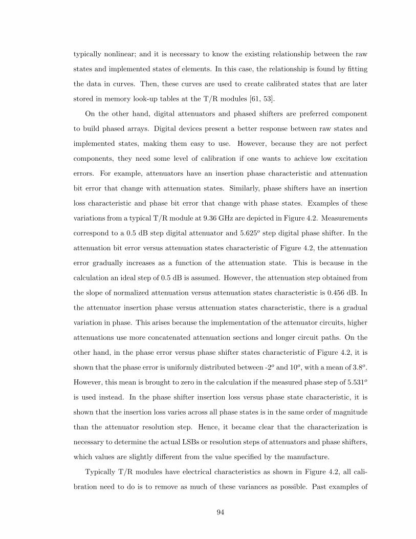
typically nonlinear; and it is necessary to know the existing relationship between the raw
states and implemented states of elements. In this case, the relationship is found by fitting
the data in curves. Then, these curves are used to create calibrated states that are later
stored in memory look-up tables at the T/R modules [61, 53].
On the other hand, digital attenuators and phased shifters are preferred component
to build phased arrays. Digital devices present a better response between raw states and
implemented states, making them easy to use. However, because they are not perfect
components, they need some level of calibration if one wants to achieve low excitation
errors. For example, attenuators have an insertion phase characteristic and attenuation
bit error that change with attenuation states. Similarly, phase shifters have an insertion
loss characteristic and phase bit error that change with phase states. Examples of these
variations from a typical T/R module at 9.36 GHz are depicted in Figure 4.2. Measurements
correspond to a 0.5 dB step digital attenuator and 5.625o step digital phase shifter. In the
attenuation bit error versus attenuation states characteristic of Figure 4.2, the attenuation
error gradually increases as a function of the attenuation state. This is because in the
calculation an ideal step of 0.5 dB is assumed. However, the attenuation step obtained from
the slope of normalized attenuation versus attenuation states characteristic is 0.456 dB. In
the attenuator insertion phase versus attenuation states characteristic, there is a gradual
variation in phase. This arises because the implementation of the attenuator circuits, higher
attenuations use more concatenated attenuation sections and longer circuit paths. On the
other hand, in the phase error versus phase shifter states characteristic of Figure 4.2, it is
shown that the phase error is uniformly distributed between -2o and 10o, with a mean of 3.8o.
However, this mean is brought to zero in the calculation if the measured phase step of 5.531o
is used instead. In the phase shifter insertion loss versus phase state characteristic, it is
shown that the insertion loss varies across all phase states is in the same order of magnitude
than the attenuator resolution step. Hence, it became clear that the characterization is
necessary to determine the actual LSBs or resolution steps of attenuators and phase shifters,
which values are slightly different from the value specified by the manufacture.
Typically T/R modules have electrical characteristics as shown in Figure 4.2, all cali-
bration need to do is to remove as much of these variances as possible. Past examples of
94

0 10 20 30 40−1
0
1
2
3
Attenuation state (dB)
Atte
nuat
ion
bit e
rror
(dB
)
0 10 20 30 40−20
0
20
40
60
Attenuation state (dB)
Atte
nuat
or in
s. p
hase
(deg
)
0 100 200 300 400−5
0
5
10
15
Phase shifter state (deg)
Pha
se e
rror
(dB
)
0 100 200 300 400−3
−2
−1
0
1
Phase shifter state (deg)
Pha
se s
hifte
r in
s. lo
ss (
dB)
0 10 20 30 40−40
−30
−20
−10
0
Attenuation state (dB)
Nor
m. a
ttenu
atio
n (d
B)
MeasuredTheoretical
0 20 40 60 80−400
−300
−200
−100
0
Phase shifter state (deg)
Nor
m. i
ns. p
hase
(dB
)
MeasuredTheoretical
Figure 4.2: Attenuator and phase shifter performance in a X-band T/R module.
how to perform this calibration are given in [57, 62, 58]. In [57], the attenuator and phase
shifter states are calibrated separately by adjusting the measured data to linear models
that represent the theoretical states of each component. In this work, two separate algo-
rithms for amplitude and phase corrections are presented. Unfortunately, this approach
cannot correct the effects of phase and insertion loss shift created by attenuators and phase
shifters, respectively. In [62], a nearest state algorithm is used to correct simultaneously
both attenuator and phase shifter performances. The algorithm is mentioned but not cov-
ered in this work. Nevertheless, it can be assumed that the algorithm works similarly as
the nearest neighbor algorithm, which can find the closest points to a desired point in the
95

measured data. This process is represented algorithmically in Figure 4.3. The attenua-
tor and phase shifter states of a T/R module are adjusted such as the norm between the
measured complex gain, Sq21(n, att, phs), and theoretical complex gain is minimized. The
optimization problem can be written as
xmin = minatt,phs
‖ Sq21(n, att, phs)− 10−LBSa.attraweLSBp.phsraw ‖ (4.10)
This expession provides a set of values for att and phs that allows the implementation
of desired complex gain given by attraw and phsraw. In practice, the translation from raw
states to calibrated states is performed using a two-dimensional look-up table stored in the
internal memory of each T/R module.
The comparison between uncorrected and corrected gain/phase maps of a typical X-
band T/R module based on a 6-bit 32 dB digital attenuator with attenuation steps of 0.5
dB, and a 6-bit digital phase shifter that provides 360o phase coverage with phase shift
steps of 5.625o are shown in Figure 4.4 and Figure 4.5. After characterization, it is found
that LSBa and LSBp are 0.456 dB and 5.531o, respectively. These values are then used
in (4.10) to find the calibrated states that correct the gain and phase variations. Finally,
the lower attenuator states in the calibrated data are discarded in order to have a uniform
gain characteristic and implement states with low calibration errors. In Figure 4.5, the
corrected gain map has a very uniformly distributed pattern through all attenuator and
phase shifter states. It should be noted the attenuation range was reduced from 64 to 60
states in order to improve the gain characteristic at the lower attenuation states, where it’s
almost impossible to achieve calibrated states with low errors. While in the corrected phase
characteristic, the spreading caused by the attenuator and phase bit error have been nearly
reduced in all the range. For this particular example, a RMS amplitude error of 0.24 dB
and RMS phase error of 1.73o are achieved. Theoretically, due to quantization errors, it is
expected an amplitude error of 0.13 dB RMS and phase error of 1.6o RMS. The amplitude
errors differences arise because the variance caused by the phase shifter on the gain.
On the other hand, the corrected gain and phase maps (see Figure 4.5) are obtained
by the combination of 60 attenuation states and 64 phase states, together, each map is
96

For each module n
For each attenuator state att
For each phase shifter state phs
attmin =0; phsmin =0; xmin=1
x < xmin
attmin=att; phsmin=phs; xmin=x
F
T
phs< 2bphs
T
F
att<2batt
T
F
rawprawaphsjLSBattLSBq
ephsattnSx.
21 10),,(
Figure 4.3: Amplitude and phase calibration algorithm for T/R modules.
comprised by 3840 states. After a comparative analysis between calibrated data and un-
calibrated data, it was found that only 2944 of the original 4096 states were used in the
creation of these maps. As result, there is a significant data reduction when elements are
calibrated.
4.2.3 Element Characterization
In principle, it is desirable to measure all possible combinations of amplitude and phase
states realized by the active elements in order to minimize the errors produced by the
calibration process. However, full calibration of an active array is measurement intensive.
It is common for array elements to have at least 6 bits at each digital attenuators and
phase shifters, when are used together, they can provide 4096 combinations of amplitude
97

0 10 20 30 40 50 60 70−5
0
5
10
15
20
25
30
Phase shifter state
Gai
n (d
B)
Uncorrected gain
0 10 20 30 40 50 60 70−200
−150
−100
−50
0
50
100
150
200
Phase shifter state
Pha
se (
degr
ee)
Uncorrected phase
Figure 4.4: Raw gain and phase map for a X-band T/R module at 9.36 GHz.
0 10 20 30 40 50 60 70−5
0
5
10
15
20
25
30
Phase shifter state
Gai
n (d
B)
Corrected gain
0 10 20 30 40 50 60 70−200
−150
−100
−50
0
50
100
150
200
Phase shifter state
Pha
se (
degr
ee)
Corrected phase
Figure 4.5: Calibrated gain and phase map for a X-band T/R module at 9.36 GHz.
98
and phase states per channel. In addition, measurements are realized at different frequency
and temperature. As a result, thousands of measurements are required to fully characterize
the performance of each element [63]. However, in practice, this procedure is avoided
if the array is large, because it will result in a large number of measurements and an
unacceptable long test time, affecting consequently the array test cost. To save time, the
number of measurements are reduced and the omitted states are then recovered from the
measurements.
In theory, the characterization could be done during the T/R modules production test,
when they are isolated, allowing measurements at different temperatures [62]. But it can
be also performed when modules are integrated on the system, connected to radiating
elements and RF feed networks. In this case, measurements are taken with a near-field
probe measurement system. A sampling probe is positioned in front of each element to be
measured and amplitude and phase data are taken for that element, while other elements
are terminated in match loads. For large arrays, the number of states to be measured from
attenuators and phase shifters will depend on a trade-off between calibration error budget
and test time [51]. While in moderate-size arrays, the measurements can be realized at
cardinal states (states contained in the set 0,1,2,4,..2Nbits ) or through all states of each
component [22, 57].
4.3 Calibration approach based on nearest state algorithm
Standard methods for array calibration assume that amplitude and phase characteristics
of active elements have been calibrated in advance. Thus, array control computers only
need to compute the amplitude and phase commands (attenuator and phase shifter raw
states) for each module. Then, correction look-up tables in T/R modules translate the
raw states into calibrated states. The data stored in the look-up tables is determined from
measurements of the amplitude and phase behavior of each individual module; only data
points that best approximate to ideal curves representing the ideal T/R module performance
are selected. One disadvantage of this approach is that many amplitude and phase states
are discarded during the creation of correction tables, reducing the ability to implement the
desired excitation function with better amplitude and phase settings.
99

The problem of interest is to calibrate a phased array antenna in the presence of a RF
beam former network with digital attenuators and phase shifters, focusing on the imple-
mentation of excitation functions with the lowest possible random errors. This goal can
be accomplished if all the amplitude and phase settings measured from each element are
available for the calibration. Optimum excitation settings are obtained if the calibration
is performed using a nearest state algorithm. The algorithm searches across all amplitude
and phase settings of each element for the values that best match the desired excitation
coefficients for a particular beam. Settings for different beams are computed and then for-
matted into binary tables (beamtable) that are unique for each T/R module. To implement
the array excitation, beamtables are stored in memory based look-up tables in the T/R
modules, where the appropriated amplitude and phase settings for each desired beam are
stored.
The proposed method assumes that gain and phase characteristics of radiating elements
have been characterized through all attenuation and phase shifter states using a NF probe.
Subsequently, these data can be used to compute the relative errors between elements (Eqn.
4.5) and ideal weighting (Eqn. 4.6) that is requered to implement the excitation function
and correct the amplitude and phase differences among elements. Let’s assume that the
array has been calibrated by the above method. When (4.5) and (4.6) are used in (4.3),
yields
Sq21(n, att, phs) = vqnCuqnref
(4.11)
This quantity represents the implemented complex gain. Now, from (4.4), Sq21(nref , 0, 0) =
Cuqnref . Hence, it follows that
Sq21(n, att, phs) = vqnSq21(nref , 0, 0) (4.12)
Note that excitation coefficient is scaled by the gain of the element that has less gain
in state zero. This condition allows the gain realized by the elements fall within the oper-
ation range of attenuators and phase shifters, or within the gain and phase range of each
element. The values att and phs in the above formula are the states that must be found at
each element to satisfy the equally (4.12). However, due to quantization effects the array
100

excitation will not be perfectly implemented. The goal of calibration is to find the proper
settings that minimize the error between the implemented complex gain Sq21(n, att, phs) and
the theoretical complex gain Sq21,theo(n), which depends on the desired aperture amplitude
distribution function (an) and the scan angle (θ0). Formally, this is expressed as
[attq(n, θ0), phsq(n, θ0)] = argmin
att,phs‖ Sq21(n, att, phs)− S
q21,theo(n, θ0) ‖ (4.13)
Sq21,theo(n, θ0) = anejnkdsin(θ0)Sq21,ref
|Sq21,ref | ≤ |Sq21(nref , 0, 0)|
In fact, the expression (4.13) works for any scaling factor less than or equal to refer-
ence gain Sq21(nref , 0, 0), its value has been replaced by S21,ref . The criteria to choose the
reference gain depends on the operation mode. For receive mode, the criteria should be
|S21,ref | ≤ min(|Sq21(n, 0, 0)|) to reduce the random excitation error and obtained better
sidelobes levels. While in transmit mode, if the amplifiers need to operates in compression,
the criteria should be S21,ref = max(Sq21(n, 0, 0)) .
To find the array calibration settings, a nearest states algorithm is used. The algorithm
searches in the measured data of each element, the best approximation for the attenuator
and phase shifter states that minimizes the norm between the measured gain Sq21(n, att, phs)
and theoretical gain S21,theo for that particular element. This process is represented algorith-
mically in Figure 4.6. This procedure gives two set of vectors attq(n, θ0) and phsq(n, θ0),
which are quantized and formatted into a binary table ( beamtable) that is unique to a
particular T/R module.
RMS amplitude and phase errors between implemented excitation and theoretical exci-
tation for each beam are computed as follow
σa(θ0) =
√√√√ 1
N
N∑n=1
(|Sq21(n, attq(n, θ0), phsq(n, θ0))| − |S21,theo(n, θ0)|
|S21,theo(n, θ0)|
)2
(4.14)
σa(θ0) =
√√√√ 1
N
N∑n=1
( 6 Sq21(n, attq(n, θ0), phsq(n, θ0))− 6 S21,theo(n, θ0))2 (4.15)
101

For each module n
For each attenuator state att
For each phase shifter state phs
q
ref
jnkd
n
q SeaphsattnSx ,21
)sin(
210),,(
attmin=0; phsmin=0; xmin=1
x<xmin
attq(n,θ)=att; phs
q(n,θ)=phs; xmin=x
F
T
T
F
T
F
phs<2bphs
att<2batt
For each scan angle θ0
T
F
θ<#beams
Figure 4.6: Amplitude and phase calibration algorithm for phase array system.
102

Theoretically, the amplitude and phase errors will depend on quantization errors created
by the attenuators and phase shifters, respectively. Those values are given by following
equations
σa,theo =
√LSB2
a
12+ std(LSBa)2 (4.16)
σa,theo =LSBp√
12(4.17)
4.3.1 Pattern Prediction
Let it be assumed that the array has been calibrated by the above method, and the
implemented array excitation for the nth element is proportional to the complex parameter
Sq21(n, att, phs). If an average embedded element pattern, fav(θ, φ), can be determined, for
example by far-field measurements, then the array radiation pattern can be computed from
(4.2) as
fa(θ, φ) = fav(θ, φ)N∑n=1
Sq21(n, attq(n, θ0), phs
q(n, θ0))ejnkdsin(θ0) (4.18)
4.3.2 Beamtable Format
The control electronic unit of each T/R module has 4K bytes (4096 x 16 bits) of RAM
that is used for storing the beamtables of that particular element, as discussed in chapter
[1]. The beamtables are arranged in memory blocks where calibration settings for different
beams and operation modes are stored. To access the calibration settings, the memory
blocks are configured in form of look-up tables, which looks up what the output should
be for any given combination of input states. The number and size of beamtables that
can be allocated in the memory depends on the number of beams, operation modes and
temperatures tables. Table 4.1 summarizes the number of beamtables that are available
for single and dual polarization when the array is calibrated for 128 and 256 beams. For
example, a dual-polarized array with 256 beams, operating in both polarization used as
minimum 4 different beamtables (one for each channel: RH, RV, TV and TH) for a single
temperature. However, the memory size can allow the implementation of a maximum of
4096/(256)=16 beamtables, which can be used to calibrate the array at other temperatures.
103

Table 4.1: Number of beamtables available in a 4K Memory look up table
Mode Numberof beams
Number ofchannels
Max. numberof beamtable
Max. number of beamtable perchannel
single 128 2 32 1(T)+31(R)
dual 128 4 32 1(TH)+1(TV)+15(RV)+15(RH)
single 256 2 16 1(T)+15(R)
dual 256 4 16 1(TH)+1(TV)+7(RV)+7(RH)
For the particular case when the element memory is configured with 4 beamtables and
256 beams, the memory configuration and memory map are depicted in Figure 4.7 . The
4*256=1024 memory locations are addressed with only 10-bits of the 12-bits wide beam
commands. The addressing command is concatenated as follows: two unused bits, one bit
for T/R signal (operation mode), one bit for H/V signal (polarization), and 8-bits for the
beamID (beam index), where, the bit T/R=0 for receive, 1 for transmit and bit H/V=0
for horizontal, 1 for vertical select the beamtable, while the beamID = 0, 1, 2, ..., 255
selects the desired beamsteering angle θ0. Assuming the normal azimuth scanning range
for the antenna is ±45o and that the beam sampling is uniformly distributed with angular
increment ∆θ = 90o/(256− 1) = 0.3529o. With these values, beamID and θ0 are related as
beamID = round
(θ0 − θinitial
∆θ
)θ0(beamID) = θinitial + ∆θ0beamID = −45 + 0.3529beamID (4.19)
The above formula generates the sequence θ0(0 : 255) = -45o, -44.6471o ,..., -0.1765o ,
0.1765o,..., 44.6471o, 45o.
For the above example, the beamtable data is comprised of 1024 16-bit wide words.
Each 16-bit words is the binary concatenation of 6 bits that specify the attenuator state, 6
bits that specify the phase shifter state, and bits H,V, T, and R, as it is indicated in Table
3.10. Based on memory configuration depicted in Figure 4.7, and the states obtained from
(4.13), the beamtable data for the nth element is computed as follows:
104

Beam Command
4096 x 16bit
RAM
A9
A7A6A5A4A3A2A1A0
A8D9D8D7D6D5D4D3D2D1D0
D10D11D12D13D14D15 H
Attenuator control
(6 bits)
Phase shifter control
(6 bits)
VTR
BeamID
(8 bits)
A10A11
T/RH/V
0 000h
0 0
255 0FFh
0 100h
0 1
255 1FFh
0 200h
1 0
255 2FFh
0 300h
1 1
255 3FFh
Beamtable for
channel RV
Beamtable for
channel RH
T/H H/V BeamID Address
Beamtable for
channel TV
Beamtable for
channel TH
Memory Map
H/VT/H BeamID[7:0]Unused[1:0]
Beam
-45
45
-45
45
-45
45
-45
45
Figure 4.7: Look up table configuration: Left: memory configuration. Right: memorymap.
beamtable(n, address) = conc2bit(H/V ), H/V , bit(T/R), T/R, phs2[5 : 0], att2[5 : 0]
address = beamID + 256bit(T/H) + 512bit(H/V )
phs2[5 : 0] = dec2bin(phsq(n, beamID), 6)
att2[5 : 0] = dec2bin(attq(n, beamID), 6)
where conc2 is the concatenate function, dec2bit is the function that converts decimal to
binary numbers and q is the channel (TH, TV, RH and RV). Finally, the beamtable is
transferred from the array controller to T/R module memories using the write memory
command (see Table 3.10 in section 3.6.4.1).
Table 4.2: Beamtable data format
TRM command beamtable length beamtable(n)16 bits 16 bits 1024x16 bit
105

4.3.3 Internal Temperature Compensation
The phased array system described in Chapter 3 is equipped with an inexpensive forced
air cooling system to prevent the T/R modules from excessive heat. A voltage-controllable
fan array that forces ambient air to circulate from the antenna base to the top, passing
through the T/R modules is used. Although the cooling system seems adequate to regulate
the heat of the active components, it has the disadvantage that system temperature varies
with the ambient temperature (or weather condition). The problem with this is that changes
in ambient temperature can causes drifts in the gain and phase of T/R modules [34]. As
a result, the overall gain in both transmit and receive array is varied from their operating
points, causing important changes in the radar parameters.
To ensure the gain and phase stability over ambient temperature, both transmit array
and receive array should be calibrated at different temperatures. However, in many solid-
state radars, the transmitters are calibrated to extract the maximum available power from
power amplifiers. The problem that arises is when transmit modules operate in saturation;
the gain drift cannot be compensated by adjusting the element gain. A solution to this
problem is to make the assumption that transmit array gain is stable with temperature and
attempt to compensate the two-way gain variation (Tx gain drift + Rx gain drift) with
the receive array gain. In fact, for this approach to be valid, it must be assumed that the
temperature drift is uniform all over the array.
In a phased array, the gain variations over temperature are caused generally by the
RF solid-states devices used in the T/R modules. Both DC and RF characteristics (cur-
rent, voltages, gain etc) of RF linear devices vary exponentially with temperature [64].
While gain in decibels and phase may vary quadratically [22] or linearly with temperature.
Particularly in the phased array testbed described in Chapter 3, it was found in the RF
component datasheets that the gain (in decibels dB) and phase variation over temperature
vary linearly with temperature. Same behavior was observed experimentally during the test
as well [65]. To model the gain, the measured gain in dB is converted to linear scale using
exponential transformation. After transformation, one finds that gain varies exponentially
with temperature.
106

Consider an active element that has been measured with a NF probe at different temper-
atures, the gain in linear scale as a function of temperature, t, can be described empirically
by the equation
Sq21(n, att, phs, t) = Sq21(n, att, phs, t0)e−(αq+jβq)(t−t0) (4.20)
where Sq21(n, att, phs, t0) is the gain in the reference temperature t0, αq represents the
gain variation coefficient (Neper/oC), βq represents the phase variation over temperature
(radians/oC). When measured gain (4.13) is expressed in dB, that is
|Sq21(n, att, phs, t)| = 20 ∗ log1010(|Sq21(n, att, phs, t0)|)−A(t− t0) (4.21)
where A = 20log10(e)αq is the gain variation over temperature in dB/oC . Note that the
phase in (4.20) and gain in dB (4.21) vary linearly with temperature, as it is shown in
Figure 4.13.
Now, let’s consider that transmit gain variation is attributed to the receive channel and
the gain drift can be compensated with the receive array. Then the modified receive array
gain for the nth element is expressed as follow
SR21(n, att, phs, t)e−(αT+jβT )(t−t0) = SR21(n, att, phs, t0)e
−(αR+αT+jβR+βT )(t−t0) (4.22)
Using (4.22) and (4.13) , we can define an expression for estimating the attenuator and
phase shifter states as a function of temperature for receive elements
[attR(n, θ0, t), phsR(n, θ0, t)] = argmin
att,phs||SR21(n, att, phs, t0)e−(α
R+αT+jβR+βT )(t−t0)
− SR21,theo(n, θ0, t0)|| (4.23)
the quantity SR21,theo(n, θ, t0) is defined as (4.13). The fact of keeping SR21,theo(n, θ, t0) con-
stant at any temperature in (4.23) obliges the adjustment of att and phs to compensate the
gain drift produced by the factor e−(αR+αT+jβR+βT )(t−t0) .
107

4.4 Experimental Evaluation
4.4.1 Test Equipment Description
The phased array calibration and antenna pattern measurements were carried out using
the near-field range system shown in Figure 4.8. The system consists of a linear scanner that
carries an open-ended waveguide as a NF probe, and a Agilent E8362B network analyzer
to measure the S-parameters. The lineal scanner is a product of Velmex inc having a travel
range of 1.5 meters. The setup of the measurement equipment is shown in Figure 4.9. The
array, network analyzer, and scanner controller are interfaced to a central computer, that
in turn, controls them. The computer also provides timing and communication, processes
the data, and records the measurements. The entire system is controlled by the user using
a GUI developed in C language.
The linear scanner is controlled from the host computer via a RS232 interface. The NF
probe position is controlled by commands that are generated by the computer and that are
sent to the scanner controller. When the probe is placed in the desired location, the system
can perform either single element measurements (i.e element characterization) or radiation
pattern measurements. To do so, the host computer first enables the array elements and
then sends trigger commands to E8362B network analyzer to perform standard S-parameter
measurements. All measurements are realized in pulsing mode. Data is transferred to the
computer via a 100 Mbps local area connection (LAN).
4.4.2 Scanner Alignment and Antenna Position Error Estimation
In order to minimize calibration errors, the linear positioner is parallel attached to the
antenna support structure, with the near-field probe aligned to the center of the subarrays.
The mechanical alignment is realized by hand using a webcam and image processing GUI
developed in Matlab [66], see figure 4.10. The alignment procedure consists in positioning
the webcam in front of each array elements and computing their positions in the array from
snapshots that are taken at those particular positions. The location errors and offsets that
are obtained from this procedure are used to correct any misalignment can exist between
the array and scanner.
108

Figure 4.8: Near field probe test system.
Data/Measurement trigger
RF port 2
RF port 1
Digital T/R module data
RS-232 serial
9.6 kbps
RS-232 serial
115 kbps
100 Mbps Ethernet
NF
probe
Linear
scanner
Computer
Near Field
Measurement
Control
Interface
(NFMCI)
Array
Control
Interface
(ACI)
ACI set:
- Operation mode:
TV,TH,RH,RV
- Attenuator/Phase shifter
states
- Beam shape
- Beam scan angle
NFMCI set:
- Probe scan range
- NF probe position
- Frequency
- Output power
Network
Analyzer
Agilent
Technology
E8362B
AUT
Linear
scanner
controller
Figure 4.9: Measurement equipment setup for phased array calibration.
To measure the element position errors, first, the linear scanner automatically aligns
the webcam with the first element of the array (i.e. the first element on the right hand
side). This point is set as the antenna origin. Then, the webcam is moved in steps equal
to the element spacing (d=17 mm), taking at each position a snapshot of each element,
untill the last element is reached. Subsequently, the GUI processes the snapshots with a
shape recognition algorithm, which recognizes the shape of microstrip patch antennas and
computes the coordinates of their centroids from the image’s center. The element location is
determined when coordinates of the centroid are added to the theoretical element position.
109

Figure 4.10: Webcam-based alignment control system
Figure 4.11 shows the example of misalignment between the array and scanner system that is
obtained with the aforementioned GUI. In this particular case, the last element in the array
(element 64) is 1.2 mm off in x direction (red curve) from the theoretical center; while in
the y direction (blue curve) one panel is 0.8 mm off in height from the other antenna panels,
this misalignment arises from fabrication defects in one of the antenna panels. Figure 4.11
also shows the discontinuities in the x direction that are produced by gaps between antenna
panels. Based on this approach, a horizontal error of 0.20 mm RMS and vertical error of
0.33 mm RMS were found. The horizontal error produces in the system a phase error of
2.32o RMS.
4.4.3 Temperature Characterization
The purpose of this test is to characterize the performance of the array elements as
a function of ambient temperatures. Since the array is not equipped with a temperature
control system that can hold a constant temperature in the array, it is necessary to esti-
mate how the gain and phase of elements changes with temperature. Although ideally it
is desirable to perform the array characterization in an environmental test chamber that
110

Figure 4.11: GUI that determine the element position errors and alignment errors
can emulate different ambient temperatures, such facility was not available for this test.
However, it can be realized if the T/R module temperature can be varied externally, and
if it is assumed that temperature dependence of manifold networks, cables, and passive
array are negligible over the temperature range. In fact, passive components usually have
low coefficients of thermal expansion that results in small changes in insertion phase with
temperature compared to the insertion phase created by solid-state devices at the same
temperature range. In this work, the T/R module temperature is controlled by adjusting
the fan speed of a fan array system, which in turn controls the temperature of the airflow
that passes through T/R modules.
The temperature characterization consists in measuring the S-parameter S21 from a cal-
ibrated array at different temperatures. To do this, first the array is calibrated at lower
temperature, when the fan array operates at maximum speed; then temperature of T/R
modules is varied in steps until it reaches the maximum temperature, that is when the fan
array is off. At each temperature step, the parameter S21 of each active element is mea-
sured when module temperature reaches steady state. Figure 4.12 shows the temperature,
gain and phase characteristics at different fan voltages as a function of time for a receive
element, right after being turned on. The time to reach steady state depends on the initial
111

0 100 200 300 400 500 60030
35
40
45
time (sec)T
empe
ratu
re (
C)
0 100 200 300 400 500 600−21.5
−21
−20.5
−20
time (sec)
|S21
| (dB
)
0 100 200 300 400 500 600172
174
176
178
time (sec)
S21
Pha
se(d
egre
e)
24V18V12V8V0V
24V18V12V8V0V
24V18V12V8V0V
Figure 4.12: Measured temperature and Transmission coefficient S21 as a function of timeand different fan voltages. Top: Temperature. Middle: S21 Magnitude. Bottom: S21 phase.
temperature, temperature constant, and pulse duty cycle. In this test, the time is between
60 sec to 500 sec.
The procedure to characterize the elements is described below:
1. Calibrate the array at low temperature, that is when fan speed is maximum.
2. Reduce the fan speeds to increase the temperature.
3. Place the NF probe in front the first element.
112

4. Pulse with a duty cycle of 30% the T/R module under test and read internal temper-
ature. Repeat this step till steady-state temperature is reached. Then, measure the
parameter S21(att, phs, t) with the network analyzer.
5. Move the NF probe to the next element and repeat steps 4 and 5 until last module is
reached.
6. Repeat steps 2 to 5 until the fan speed is zero, point where the temperature is maxi-
mum.
It should be noted that, while in receive the temperature characterization is realized in
the linear region, in transmit the characterization is realized using the power amplifiers in
the saturation region. Figure 4.13 shows the average gain, phase and Tx saturation power
characteristics versus module temperature for both Tx and Rx elements, at central frequency
of 9.36 Ghz. Measurements are normalized to the temperature of 34 oC. According to the
results, the receive gain and phase variation over temperature are 0.061 dB/oC and 0.43
deg/oC, respectively. The total gain loss is about 1.1 dB in the range. The gain variation
over temperature is dominated specially by the thermal characteristics of three amplifiers
(HMC441LP3 and HMC564LC4) used in the receive channel, the manufacturer specifies
a typical gain variation of 0.2 dB/oC for each component. In contrast, the Tx saturation
power and Tx phase vary in at rate of 0.009 dB/oC and 0.45 degree/oC respectively, being
the total power variation 0.14 dB in the range of interest. The small variation in the
transmit saturation power is because the power amplifier is heavily compressed.
Based on above results, the gain for transmit and receive elements can be modeled using
(4.20) or (4.21). For receive mode, α = A/(20 ∗ log10(e)) = 0.061/8.68 = 0.0079 Neper/oC
and β = 0.43 ∗ π/180 = 0.0075 radians/oC, thus the gain can be written as
SR21(n, att, phs, t) = SR21(n, att, phs, t0)e−(0.0070+j0.0075)(t−t0) (4.24)
|SR21(n, att, phs, t)|(dB) = 20log10(|SR21(n, att, phs, t0)|)− 0.061(t− t0)
the reference gain SR21(n, att, phs, t0) is selected at temperature to. While for transmit mode,
α = 0.001 Neper/oC and β = 0.0079 radians/oC. Hence, using (4.20) or (4.21), it follows
that
113

32 34 36 38 40 42 44 46 48 50 52−2
−1.8
−1.6
−1.4
−1.2
−1
−0.8
−0.6
−0.4
−0.2
0
Module Temperature (°C)
Rel
ativ
e M
agni
tude
32 34 36 38 40 42 44 46 48 50 52−10
−9
−8
−7
−6
−5
−4
−3
−2
−1
0
Pha
se (
deg)
Rx Gain (dB)Tx Sat. Power (dBm)
Rx PhaseTx Phase
Figure 4.13: Relative gain, phase and saturation power performance versus module tem-perature.
ST21(n, att, phs, t) = ST21(n, att, phs, t0)e−(0.001+j0.0079)(t−t0) (4.25)
|ST21(n, att, phs, t)| = 20log10(|ST21(n, att, phs, t0)|)− 0.009(t− t0)
Finally, although the gain was only modeled for the temperature range 34 oC - 52 oC,
it is not clear if the linear characteristic of the gain in decibels can be extended to 0 oC .
But assuming that the linear model is still valid for a temperature range from 0 oC to 54
oC, we will expect a Rx gain variation of 3.0 dB and Tx saturation power variation of 0.45
dBm into the range. These values suggest that the array will need an internal calibration
system to correct the gain drift due to temperature changes.
4.4.4 Receive Array Calibration
In principle, it is desirable to measure all possible combinations of amplitude and phase
states realized by the active elements in order to minimize the errors produced by the cali-
bration process. But, the time to reach the steady-state temperature and time to measure
the 4096 states (64x64) at difference frequencies of each element will result in unaccept-
114
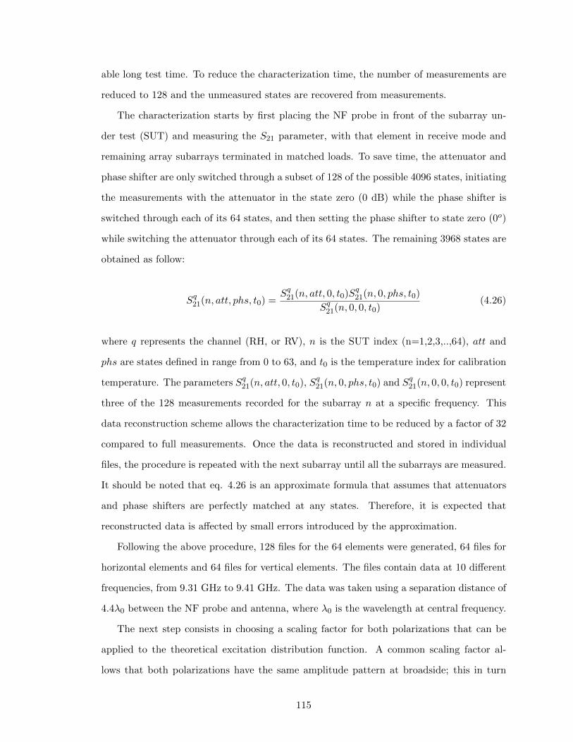
able long test time. To reduce the characterization time, the number of measurements are
reduced to 128 and the unmeasured states are recovered from measurements.
The characterization starts by first placing the NF probe in front of the subarray un-
der test (SUT) and measuring the S21 parameter, with that element in receive mode and
remaining array subarrays terminated in matched loads. To save time, the attenuator and
phase shifter are only switched through a subset of 128 of the possible 4096 states, initiating
the measurements with the attenuator in the state zero (0 dB) while the phase shifter is
switched through each of its 64 states, and then setting the phase shifter to state zero (0o)
while switching the attenuator through each of its 64 states. The remaining 3968 states are
obtained as follow:
Sq21(n, att, phs, t0) =Sq21(n, att, 0, t0)S
q21(n, 0, phs, t0)
Sq21(n, 0, 0, t0)(4.26)
where q represents the channel (RH, or RV), n is the SUT index (n=1,2,3,..,64), att and
phs are states defined in range from 0 to 63, and t0 is the temperature index for calibration
temperature. The parameters Sq21(n, att, 0, t0), Sq21(n, 0, phs, t0) and Sq21(n, 0, 0, t0) represent
three of the 128 measurements recorded for the subarray n at a specific frequency. This
data reconstruction scheme allows the characterization time to be reduced by a factor of 32
compared to full measurements. Once the data is reconstructed and stored in individual
files, the procedure is repeated with the next subarray until all the subarrays are measured.
It should be noted that eq. 4.26 is an approximate formula that assumes that attenuators
and phase shifters are perfectly matched at any states. Therefore, it is expected that
reconstructed data is affected by small errors introduced by the approximation.
Following the above procedure, 128 files for the 64 elements were generated, 64 files for
horizontal elements and 64 files for vertical elements. The files contain data at 10 different
frequencies, from 9.31 GHz to 9.41 GHz. The data was taken using a separation distance of
4.4λ0 between the NF probe and antenna, where λ0 is the wavelength at central frequency.
The next step consists in choosing a scaling factor for both polarizations that can be
applied to the theoretical excitation distribution function. A common scaling factor al-
lows that both polarizations have the same amplitude pattern at broadside; this in turn
115

0 10 20 30 40 50 60 70−40
−35
−30
−25
Rel
ativ
e am
plitu
de (
dB)
Element index
← −37.3 H polV pol
0 10 20 30 40 50 60 70−200
−100
0
100
200
Rel
ativ
e ph
ase
(deg
rees
)
Element index
H polV pol
Figure 4.14: Measured transmission coefficient S21 for receive array at state zero. Top:Relative amplitude. Bottom: Relative phase
will allow the polarimetric calibration of vertical and horizontal channels. To choose this
factor, it is necessary first to determine the lowest S21 among elements when attenuators
and phase shifters are set to state zero. Figure 4.14 shows the measured amplitude and
phase distribution for the transmission coefficient S21 at state zero across the array. It is
important note that amplitude and phase disparities for a given polarization are caused
by hardware differences among elements. While gain differences between polarization in
a particular element is due to losses between T/R modules and radiators, which can be
caused by some imperfection in T/R module connectors, antenna connectors, and loose
interconnection cable. For the uncalibrated test array, the amplitude and phase variations
at both polarizations are less than 1.3 dB RMS and 100.3o RMS, respectively. In addition,
the lowest amplitude value is -37.3 dB, which is found at the element 30. To minimize the
RMS excitation error after calibration, it is necessary that the scaling factor should be less
than or equal to lowest S21; for this test, the chosen value is -39 dB.
The calibration is performed to implement a -25 dB n=2 Taylor taper. Normalized
amplitude coefficients are scaled by the scaling factor, and results are then used by the
116

0 10 20 30 40 50 60 70−48
−46
−44
−42
−40
−38
Element number
Rel
ativ
e am
plitu
de (
dB)
TheoreticalStandard calibrationNear state algorithm
0 10 20 30 40 50 60 70−8
−6
−4
−2
0
2
4
6
8
Element number
Rel
ativ
e ph
ase
(deg
ree)
TheoreticalStandard calibrationNear state algorithm
Figure 4.15: Comparison of calibrated transmition coefficiente S21 in receive mode . Top:Amplitude distribution. Bottom: Phase distribution
calibration algorithm to compute the element setting that implements the desired taper.
For the purpose of demonstrating the improvement of RMS errors, the standard calibration
is also implemented. Both calibrations are carried out at central frequency of 9.36 GHz. The
amplitude and phase as determined by standard calibration and by the proposed approach
are shown in figure 4.15 . The RMS errors, which are the main indicators of the performance,
are shown in Table 4.3. The theoretical error were calculated from ( 4.16) and (4.17), using
the measured values LSBa=0.46 dB, std(LSBa)=0.1671 dB, LSBp= 5.51o; while RMS
errors for the other two methods were calculated using (4.14)-(4.17). Table 4.3 shows that
RMS errors obtained from calibration based on nearest state algorithm are close to the
theoretical values and better than the values obtained from standard calibration.
In order to evaluate the array calibration, the calibrated settings are loaded in the T/R
modules to measure the far-field radiation patterns. In this case, the figure of merit is
117

−40 −30 −20 −10 0 10 20 30 40−40−35−30−25−20−15−10
−50
Azimuth (deg)
Nor
mal
ized
Am
plitu
de (
dB)
−40 −30 −20 −10 0 10 20 30 40−40−35−30−25−20−15−10
−50
Azimuth (deg)
Nor
mal
ized
Am
plitu
de (
dB)
H polarizationTheoretical
V polarizationTheoretical
Figure 4.16: Theoretical and measured azimuth far field patterns at 9.36GHz, derived fromNear-Field measurement. Top: H polarization. Bottom: V polarization.
how well the calibrated pattern approaches the theoretical pattern. In the experiment, the
fields are measured in the near-field range. But they are transformed to far-field applying a
Fourier transform. Additionally, an idealized probe correction is applied to data to remove
the probe effects. The resulting normalized azimuth patterns and theoretical pattern in
receive, for V and H polarization at 0o scan angle are depicted in figure 4.16. The results
are excellent based on the null locations and because there is not a large deviation in the
peak sidelobes between measured and theoretical patterns. At 4.13o, the increment in the
larger sidelobes peak is 0.32 dB in the horizontal polarization and 0.76 dB in the vertical
polarization.
Table 4.3: Comparison of RMS excitation errors for calibrated array in receive
Method RMS amplitude error (dB) RMS phase error (degrees) Total error (σ)
Theoretical 0.21 1.59 0.037
Standard calibration 0.30 2.14 0.051
Nearest state algorithm 0.23 1.61 0.038
118

4.4.5 Transmit Array Calibration
The calibration goal for the transmit array is slightly different from the receive array.
While in receive, the goal is to implement a Taylor-weighted amplitude taper that provides
a radiation pattern with low sidelobes, in transmit the goal is to implement a uniform
illumination using the maximum power available in the T/R modules. In order to use the
maximum available output power, all transmit modules are operated in compression. This
leads the array to lose the ability to control the gain. Having no gain control, the phase is
the only parameter that needs to be characterized. To calibrate the transmit array with its
modules in compression, an extra test is performed before the element characterization. The
test consists in measuring the output power variations of each element versus the antenna
input power with the NF probe. Test is done after setting the attenuator and phase shifter
in the state zero. Measurements allow the determination of the minimum power (Pin1dB)
that should be applied in the antenna input to operate the T/R modules under saturation.
Once this boundary is found, an input power level greater than Pin1dB is applied to the
antenna and the elements are characterized.
Figure 4.17 shows the average output power from 64 elements in both polarizations
sensed with the NF probe versus the antenna input power. The standard deviation of the
sensed output power was 0.92 dBm and 0.74 dBm for V and H polarization, respectively.
The variance of these parameters is due in part to the interconnection losses between the
T/R modules and the array elements, which is realized with push-on SMP connectors. The
average (Pin1dB) is around 30 dBm. Above this point, any power level will be enough to
saturate the modules.
For this experiment, the element characterization is performed using an input power
of 35 dBm. The procedure used to measure the parameter S21 is similar to the receive
elements. Although only the phase shifter should be characterized, the attenuator is also
characterized to improve the phase resolution. The improvement in the phase steps is
because the element insertion phase also changes as a function of the attenuation states,
being its phase slope less than phase slope produced by phase shifter. As a result, the total
phase can be controlled by adjusting both the attenuator and phase shifter. In contrast, in
the standard calibration, the phase is only controlled by the phase shifters.
119

5 10 15 20 25 30 35−20
−15
−10
−5
0
5
10
Input Power (dBm)
Sen
sed
Out
put P
ower
(dB
m)
V polarizationH polarization
Figure 4.17: Average output power and error bars versus input power
In order to operate the array in compression, the scaling factor is chosen equal to the
maximum S21 across the array. Figure 4.18 shows the corresponding amplitude (compressed
gain) and phase distribution for the transmission coefficient S21 in both polarizations when
measured in state zero. The amplitude errors are less than 0.89 dB RMS and the phase
errors are less than 31.6o RMS, while the maximum S21 is 1.3 dB.
After choosing the scaling factor, the nearest state algorithm is used to determinate
the calibration settings that provide the uniform illumination to array. In addition, array
calibration is performed using the standard calibration to compare the results obtained
from both methods. The amplitude and phase settings for the vertical polarization obtained
from the two calibration methods are depicted in Figure 4.19. The top graph shows that the
amplitude distribution is not affected by the calibration as expected. While the lower graph
shows that phase distribution obtained from the nearest state algorithm is better than the
one obtained with the standard calibration. Table 4.4 shows that the RMS phase error
obtained with nearest state algorithm is even better than the theoretical error (Calculated
from phase shifter characteristic). The improvement is due to the extra phase shift created
by the attenuator.
120

0 10 20 30 40 50 60 70−4
−2
0
2
Element numberR
elat
ive
ampl
itude
(dB
)
1.3 →
V polarizationH polarization
0 10 20 30 40 50 60 70−100
−50
0
50
100
Element number
Rel
ativ
e ph
ase
(deg
)
V polarizationH polarization
Figure 4.18: Measured transmition coefficiente S21 for transmit array at state zero. Top:Amplitude distribution. Bottom: Phase distribution
Table 4.4: Comparison of RMS excitation errors for calibrated array in transmit
Method RMS amplitude error (dB) RMS phase error (degrees) Total error (σ)
Theoretical - 1.59 0.102
Standard calibration 0.82 2.02 0.105
Nearest state algorithm 0.82 1.01 0.100
Unfortunately, due to laboratory safety issues, the radiation patterns from transmit
array could not be measured in the near-field range. Rather, the patterns are predicted
using (4.13). Figure 4.20 shows the predicted far-field radiation patterns at the central
frequency 9.36 GHz. The patterns achieved peak sidelobe levels of -12.4 dB and -13.3 dB
in the vertical and horizontal polarization respectively. The peak sidelobe level for the
vertical polarization exceeds in 0.9 dB the expected value for a uniform distribution. This
degradation is due to RMS amplitude errors of the implemented amplitude, which can not
be calibrated.
121

0 10 20 30 40 50 60 70−4
−3
−2
−1
0
1
2
Element number
Rel
ativ
e am
plitu
de (
dB)
TheoreticalStandard calibrationNear state algorithm
0 10 20 30 40 50 60 70−8
−6
−4
−2
0
2
4
6
8
Element number
Rel
ativ
e ph
ase
(deg
ree)
TheoreticalStandard calibrationNear state algorithm
Figure 4.19: Comparison of calibrated transmission coefficient S21 in transmite mode. Top:Relative amplitude distribution. Bottom: Relative phase distribution.
4.5 Scanning performance
The purpose of this test is two-fold: first, to evaluate the array calibration at different
scan angles. Second, to measure the array characteristic as a function of the scan angle.
Part of this information will be useful to define the radar system equation. During the test,
the array was calibrated such that it could generate 255 beams (using 25dB Taylor taper) at
each polarization, ranging from -45o to 45o with uniform increment of 0.354o. Calibration
data is stored in the T/R module’s beamtables in order to measure all beams in a single
pass of the near-field scanner. Measurements in receive mode are only performed.
The procedure to measure the radiation pattern in a polarization is described below:
1. Calibrate the array for 255 beams and load the setting in the module’s beamtables.
122

−40 −30 −20 −10 0 10 20 30 40−40
−30
−20
−10
0
Azimuth (deg)
Rel
ativ
e A
mpl
itude
(dB
)
−−−SLL= −12.4 dB
V polarizationTheoretical
−40 −30 −20 −10 0 10 20 30 40−40
−30
−20
−10
0
Azimuth (deg)
Rel
ativ
e A
mpl
itude
(dB
)
−−−SLL= −13.3 dB
H polarizationTheoretical
Figure 4.20: Theoretical and predicted azimuth far field patterns at 9.36 GHz. Top: Vpolarization. Bottom: H polarization.
2. Load sequence table for the first 8 beams (4 beams for receive and 4 beams for trans-
mit). Transmit commands are loaded with settings that unable the transmit function.
3. Place the NF probe in front the first sampling position.
4. Pulse the array with a duty cycle of 30% until steady-state temperature is reached.
5. Measure the parameter S21 for each beam given by the sequence table
6. Load a sequence table for the next 4 beams repeat step 5 and 6 until the last table
with the last beam is measured.
7. Move the NF probe to the next sampling position and repeat steps 5 to 7 until the
last sampling position is reached.
8. Rotate 90o the NF probe to measure the cross-polar component and return to step 2.
9. Transform near-field patterns to far-field pattern. Then, apply the theoretical probe
correction.
10. Determine beamwidth, sidelobe level, and beam pointing accuracy for each beam.
123
Figure 4.21: Overlay of 255 far field radiation pattern measurements, derived from Near-field measurements. Top: Horizontal polarization. Bottom: Vertical polarization
Figure 4.21 shows the measured far-field patterns (for 255 beams) at the azimuth plane
for the main components of each polarization. Patterns have been normalized to the max-
imum gain at broadside. The density plot looks a little crowded, but one can clearly see
how the scanned gain changes with scan angle. The scanned gain rolls off at larger scan
angles because the element pattern rolls off.
Figure 4.22 and 4.23 show the co-polar and cross-polar patterns at azimuth plane for
both H and V polarization, only 47 beams have been plotted to simplify the data visual-
ization. It is important to note in both figures that calibration only works for the main
components, and that the cross-polar patterns are always 30 dB lower than the co-polar
patterns. These results corroborate the results of previous measurements that were ob-
tained using element pattern measurements [67]. Additionally, Figure 4.22 and 4.23 also
show the beamwidth broadening effect that occurs when the beam is steered off broadside.
124

−60 −40 −20 0 20 40 60−50
−40
−30
−20
−10
0
φ (deg)
Eh(
φ,θ=
90)
Copolar
−60 −40 −20 0 20 40 60−50
−40
−30
−20
−10
0
φ (deg)
Ev(
φ,θ=
90)
Cross−pol
Figure 4.22: Overlay of 47 far field radiation patterns for receive mode, horizontal polar-ization. Top: Copolar pattern. Bottom: Cross polar pattern
−60 −40 −20 0 20 40 60−50
−40
−30
−20
−10
0
φ (deg)
Eh(
φ,θ=
90)
Cross−pol
−60 −40 −20 0 20 40 60−50
−40
−30
−20
−10
0
φ (deg)
Ev(
φ,θ=
90)
Copolar
Figure 4.23: Overlay of 47 far field radiation patterns for receive mode, vertical polarization.Top: Cross polar pattern. Bottom: Copolar pattern
125

−50 −40 −30 −20 −10 0 10 20 30 40 50−2.5
−2
−1.5
−1
−0.5
0
0.5
Scan angle (deg)
Nor
mal
ized
Am
plitu
de (
dB)
H polV pol
Figure 4.24: Measured gain envelope for receive horizontal and vertical polarization.
The scanning performance is verified by estimating the amplitude and phase of the main
beam at the beam scan angle. The gain envelope (also called scanned gain or average active
element pattern) for H and V polarization as a function of scan angle is depicted in Figure
4.24. The asymmetry in the plot about 45o occurs due to the active element pattern roll-off,
which depends on the mutual coupling and array tolerances (i.e. variations in the radiating
elements or panel misalignment). The gain loss is less than 2.5 dB when the beam is steered
to ± 45o. The ripple present in the gain envelope is caused by the variance of the main beam
peak due to excitation errors. The variance of the main beam peak is directly proportional
to the amplitude mean error caused by attenuator quantization errors.
Figure 4.25 shows the main beam phase as function of the azimuth scan angle. The
phase for H polarization is almost identical to the phase in V polarization.
4.5.1 Sidelobes
As mentioned above, the calibration goal in receive is to implement a -25 dB Taylor
amplitude distribution with low random errors. This illumination creates theoretically a
126

−50 0 50−200
−150
−100
−50
0
50
100
150
200
Scan angle (deg)
Mai
n be
am p
hase
(de
g)
H polV pol
Figure 4.25: Measured phase for main beam peak in receive horizontal and vertical polar-ization.
radiation pattern having sidelobes that are always below -25 dB level. However, in practice
when the beam is steered, some sidelobes can exceed the sidelobe level because of the
element pattern roll off. The evaluation of maximum and first normalized sidelobe peaks
at both polarizations as a function of scan angle for the calibrated array is shown in Figure
4.26. The sidelobes vary randomly with scan angle because the excitation errors change
with the implementation of each beam. While the level for the first sidelobes is better that
-24 dB in all the range, the maximum sidelobe increases up to -22 dB when the beam is
steered to ±45o. The increase is because the gain loss falls off about 2.5 dB at 45o.
4.5.2 Beamwidth
The half power beamwidth at broadside of a phased array that uses a 25 dB n = 2
Taylor taper is θ3dB(θ = 0) = 1.76o. When the beam is steered to scan angle θ0, the scanned
beamwidth is increased from the broadside beamwidth to θ3dB(θ0) = θ3dB(θ = 0)/cos(θ).
The measured and theoretical scanned beamwitdh as a function of the azimuth scan angle
127

−50 −40 −30 −20 −10 0 10 20 30 40 50−30
−29
−28
−27
−26
−25
−24
−23
−22
−21
−20
Azimuth scan angle (deg)
Nor
mal
ized
pea
k si
delo
bes
(dB
)
H pol (max SLL)V pol (max SLL)H pol (first SLL)V pol (first SLL)
Figure 4.26: Measured sidelobe peaks versus azimuth scan angles.
are shown in Figure 4.27. The results are very good; the beamwidth performance with
scanning is virtually identical. The maximum beamwidth is about 2.45o at ±45o, resulting
in a 42.4% beam broadening.
4.5.3 Beam Pointing Error
Typically, beam-pointing errors are small in medium and large phased arrays, and when
it is given as a fraction of beamwidth, its value increases proportionally with the variance
of random errors. For the calibrated array using 255 beams and 0.354o beam increments,
the beam pointing error as a function of the azimuth scanning angle is shown in Figure
4.28. The variance of beam point error with scan angle is originated by excitation errors.
In addition, it is noted an anti-symmetric behavior of pointing error, which does not have
an explanation. The beam pointing error has a maximum value of 0.06o and RMS error
across the range of 0.0125o, both values are small compared to beamwidth. The theoretical
standard deviations are evaluated using the theoretical values given in Table 4.3 in the
128

−50 −40 −30 −20 −10 0 10 20 30 40 501.5
1.6
1.7
1.8
1.9
2
2.1
2.2
2.3
2.4
2.5
Azimuth scan angle (deg)
Bea
mw
idth
(de
g)
H polV pol
θ3dB
(θ0=0)/cos(θ
0)
Figure 4.27: Comparison between theoretical and measured beamwith as a function of scanangle.
following equation [68]
∆θRMS =2√
3(σ2δ + σ2φ)
kdN3/2=
2√
3(0.02452 + 0.00952)
196.03 ∗ 17x10−3 ∗ 643/2= 5x10⁻⁵rad = 0.0029o
this value is very small compared to the measured value.
In order to demonstrate the minimum scan angle increment that can implemented by
the system, the array is calibrated in the scanning range of ±1o using 255 beams with
0.025o increments (2*RMS beam point error = 2*0.0125). The resulting error for the V
polarization pattern is depicted in Figure 4.29. The plot shows that the beam pointing
error does not excess the scan angle increment of 0.025o. The result is interesting because
the array can provide excellent pointing accuracy using 6 bit phased shifters with 5.625o
resolution steps.
129
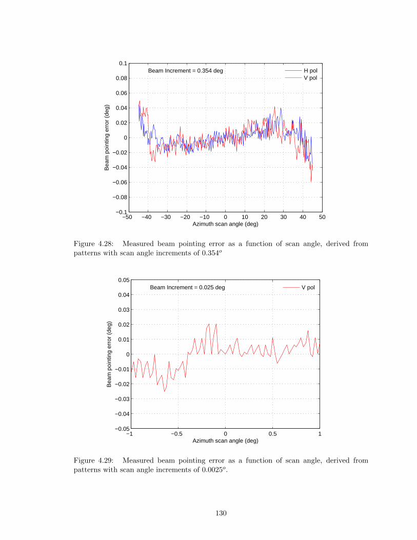
−50 −40 −30 −20 −10 0 10 20 30 40 50−0.1
−0.08
−0.06
−0.04
−0.02
0
0.02
0.04
0.06
0.08
0.1
Azimuth scan angle (deg)
Bea
m p
oint
ing
erro
r (d
eg)
Beam Increment = 0.354 deg H pol
V pol
Figure 4.28: Measured beam pointing error as a function of scan angle, derived frompatterns with scan angle increments of 0.354o
−1 −0.5 0 0.5 1−0.05
−0.04
−0.03
−0.02
−0.01
0
0.01
0.02
0.03
0.04
0.05
Azimuth scan angle (deg)
Bea
m p
oint
ing
erro
r (d
eg)
Beam Increment = 0.025 deg V pol
Figure 4.29: Measured beam pointing error as a function of scan angle, derived frompatterns with scan angle increments of 0.0025o.
130

4.5.4 Active Element Pattern and Pattern Prediction
The measurement of the average active element pattern is important because it can
help to answers some questions that arise from the system, for example: are the transmit
and receive average element patterns the same?, are the average active element pattern and
scanned gain the same?, can the scanning performance predicted from measurements of the
element pattern?. Answering the first question can help to demonstrate that all tests and
results obtained from the receive array can be also applied to transmit array. Thus, one can
avoid measuring the radiation patterns from the transmit array if one has no antenna range
facilities to perform such measurements. The second and third question are investigated for
the purpose of predicting the array performance.
In this test, the radiation patterns for 64 elements in both transmit and receive mode,
and in H and V polarization were measured. At each mode, the near-field data for 64 ele-
ments is collected in a single pass of the near-field scanner. Then, the data was processed
to obtain the far-field radiation patterns. The embedded element patterns for a set of 64
elements on each mode (RH, RV, TH, TV) are shown in Figure 4.30. The measurement
frequency is 9.36 GHz and the azimuth range is ±80o. Note that gain variations among pat-
terns are due to hardware differences. Additionally, each element has a different embedded
element pattern, which depends on the mutual coupling effect and element positions.
To calculate the average embedded element pattern, it was necessary to align the pat-
terns at broadside so that the broadside response from all elements were the same. Then,
at each angular position, the average was calculated. Figure 4.31 and 4.32 show the average
embedded element pattern for transmit and receive, in V and H polarizations. The results
demonstrate that patterns in transmit and receive are identical in both polarizations. In
H polarization, the patterns have a null at around ±62o, where a blind spot occurs. The
blidness is created by the effecf of surfaces waves close to the position of the grating lobe
[67]. While in V polarization, the patterns exhibit a smooth roll off that end at ±90o.
The element pattern and mutual coupling effects are subsumed into the average em-
bedded element pattern; which is an important design factor because it describes how the
array performs with scan and whether blind angles exist. The overall radiated power is
the product of average embedded element pattern and the isotropic array factor scanned to
131

−50 0 50−40
−30
−20
−10
Azimuth (deg)
ER
H (
dB)
Receive, H pol
−50 0 50−10
0
10
20
Azimuth (deg)
ET
H (
dB)
Transmit, H pol
−50 0 50−40
−30
−20
−10
Azimuth (deg)
ER
V (
dB)
Receive, V pol
−50 0 50−10
0
10
20
Azimuth (deg)E
TV (
dB)
Transmit, V pol
Figure 4.30: Overlay of 64 elements pattern measurements, derived from near-field mea-surements.
the proper angle (this is represented mathematically in 4.2). Since the average embedded
element pattern is an envelope of array gain versus scan angles, its effect is similar to the
term “scanned array gain” that has been obtained from a set of scanned radiation patterns
when all elements are excited (see figure 4.24). Ideally, the terms “average embedded ele-
ment pattern” and “scanned array gain” are the same. But in practice, they can differ if
the scanned array gain is affected by random excitation errors.
The top graph of Figure 4.33 shows the comparison between the average embedded
element pattern and scanned gain for the array in receive and H polarization, in the scanning
range ±45o (data is also used in Figures 4.24 and 4.32). It is clear that both curves have the
same behavior with scan angles, but the scanned gain is affected by ripples. The amplitude
and angular position of each ripple depend on array size and quantization errors that are
produced by attenuator and phase shifter settings. While the lower graph of Figure 4.33
shows the comparison between the average embedded element pattern and scanned gain in
transmit and H polarization. Note that ripples in transmit are much lower than in receive in
132

−80 −60 −40 −20 0 20 40 60 80−25
−20
−15
−10
−5
0
Azimuth (deg)
Nor
mal
ized
Am
plitu
de (
dB)
Receive V−polTransmit V−pol
Figure 4.31: Average embedded element pattern for V polarization.
−80 −60 −40 −20 0 20 40 60 80−30
−25
−20
−15
−10
−5
0
Azimuth (deg)
Nor
mal
ized
Am
plitu
de (
dB)
Receive H−polTransmit H−pol
Figure 4.32: Average embedded element pattern for H polarization.
133

spite of having a larger RMS errors. The ripples are caused by variations in the amplitudes
of the main beam with scan angle; the fractional error of the scanned gain at a specific
scan angle with respect to the average gain is proportional to the mean amplitude error of
elements, which depends on the attenuator quantization error. It should be pointed out
that for large arrays this effect is negligible, but in small and medium-size phased array, the
ripple effects can be notable. In transmit mode, on the other hand, the amplitude errors
are large because the amplitude cannot be calibrated, but their variance with scan angle is
almost negligible because modules operate in compression. As a result, the scanned gain
presents low ripples with respect to receive mode.
The data shown in Figure 4.33 is important because it describes how the radar antenna
gain (one-way gain) performs with scan angle. Ultimately, this data should be stored in
a look-up table or should be fit to a curve in order to calibrate the radar system. Figure
4.34 shows how the radiation pattern is affected by the average embedded element pattern
roll-off.
The average embedded element pattern can also be used to predict the radiation pattern
and scanned gain of a phased array using (4.18). Typically, the radiation patterns of a
phased array are measured in an antenna test facility before fielding the radar (or during
radar calibration in the field). Once the radar is deployed, the patterns must be predicted
routinely to verify that the array is operating within the specifications. This can be done
during array maintenance. There are two scenarios where the pattern prediction can results
necessary: first when the array is recalibrated, and second when the built-in-test system
detects the presence of failed modules.
For the purpose of demonstrating the utility of pattern prediction, two examples are
shown in Figure 4.35 and 4.36. In Figure 4.35, the comparison between measured and
predicted radiation patterns at V polarization for a 0o scan angle is shown. Measurements
are made when there are not failed modules. The results are good based on the sidelobe
level and null locations. In Figure 4.36, the comparison between measured and predicted
scanned array gain is shown. The predicted curve is obtained after predicting 255 different
beams (using eqn. (4.18)). Clearly, the agreement between measurement and prediction is
134

−50 −40 −30 −20 −10 0 10 20 30 40 50−2.5
−2
−1.5
−1
−0.5
0
0.5
Azimuth scan angle (deg)
Nor
mal
ized
Am
plitu
de (
dB)
Receive H polarization
AEPscanned gain
−50 −40 −30 −20 −10 0 10 20 30 40 50−2.5
−2
−1.5
−1
−0.5
0
0.5
Azimuth scan angle (deg)
Nor
mal
ized
Am
plitu
de (
dB)
Transmit H polarization
AEPTx scanned gain
Figure 4.33: Comparison between average embedded element pattern and scanned gain inH polarization.
good in terms of roll off and ripples locations. An error of 0.042 dB RMS was calculated
between the two data sets.
4.6 Temperature Compensation
In the temperature test described in section 4.3.3, the element characteristics were mea-
sured as a function of T/R module temperature, as it is shown in Figure 4.13. Results
revealed that the gain in decibels (dB) and phase in both transmit and receive mode vary
linearly with temperature. For the temperature range from 34oC to 52oC, the gain drift
was 1.1 dB in receive and 0.16 dB in transmit. It is important to note that a radar system
135

−80 −60 −40 −20 0 20 40 60 80−40
−35
−30
−25
−20
−15
−10
−5
0
5
10
Azimuth (deg)
Nor
mal
ized
Am
plitu
de (
dB)
Measured Patterns (64 beams), H polAEP, H pol
Figure 4.34: Overlay of average embedded element pattern (AEP) and 64 radiation patternmeasurements.
using this array, in the same temperature range, will have a two-way antenna gain drift of
1.26 dB. However, the drift can even result in a larger value if the temperature range is
extended. For example, a two-way gain variation of 3.64 dB can be obtained if the temper-
ature is varied from 0oC to 52oC. Evidently this can cause problems of bias in the radar
reflectivity measurements. To avoid the bias errors, the array gain must be calibrated for
different temperatures.
To demonstrate the temperature compensation technique in the system, the receive
array was calibrated for providing a constant gain in the range from 34oC to 54oC. We
assumed that reference temperature is 34oC and that 14 beamtables are enough to calibrate
the array at 14 different temperatures. The two-way gain drift in dB of each module is given
by
|∆S21| = (AR +AT )(tH − tL) = (0.061 + 0.009)(54− 34) = 1.4dB
where AR and AT are the gain variations over temperature in receive and transmit, re-
spectably; which values have been characterized in section (4.4.3). For a look-up table with
136

−60 −40 −20 0 20 40 60−50
−45
−40
−35
−30
−25
−20
−15
−10
−5
0
Azimuth (deg)
Nor
mal
ized
Am
plitu
de (
dB)
MeasuredPredicted
Figure 4.35: Comparison between measured and predicted radiation patterns at broadside.
14 beamtables, the gain increment between tables is ∆G = 1.4dB/14 = 0.1dB; which im-
plies that array gain is incremented in intervals of 0.1 dB. Similarly, the temperature step
(temperature least significant bit) between beamtables is LSBtemp = ∆G/(AR + AT ) =
0.1/(0.061 + 0.009) = 1.4286oC; which implies the array gain must be adjusted in tempera-
ture intervals of 1.4286 oC. Therefore, the beamtables are calculated for temperature values
t= 34, 35.43, 36.86, 38.29, 39.71, 41.14, 42.57, 44, 45.43, 46.86, 48.29, 49.71, 51.14, 52.57. To
select the beamtable, the average temperature of T/R modules must be computed. Then,
the temperature index (tn=0,1,2,...13) that address the beamtable is computed as
tn = round
(t− t0
LSBtemp
)= round
(t− 34
1.4286
)
where t is the average temperature in the T/R modules. The index tn is calculated and
formatted with other settings into binary commands by the array controller. Ultimately,
these commands are broadcasted to T/R modules to control the beamtables.
137

−50 −40 −30 −20 −10 0 10 20 30 40 50−3
−2.5
−2
−1.5
−1
−0.5
0
0.5
Azimuth scan angle (deg)
Nor
mal
ized
Am
plitu
de (
dB)
Measured, H polPredicted, H pol
Figure 4.36: Comparison between measured and predicted scanned gain in receive H po-larization.
To calibrate the array, one must choose a scaling factor at least 1.4 dB less than the
lowest S21 at state zero (see Figure 4.14) As demonstrated in the section 4.4.4, an initial
scaling factor of -39 dB was used to calibrate the receive array. However, to perform the
temperature compensation here, the scaling factor is chosen to be -41 dB. Thus, any gain
degradation due to temperature can be compensated by increasing element gains from -41
dB to -39 dB. Now, using the values computed in section 4.4.3, αR = 0.007 and αT = 0.001,
in (4.23) and substituting, t − t0 = 1.4286tn, the calibration algorithm for this problem is
defined as
138

[attR(n, θ0, tn), phsR(n, θ0, tn)] = argminatt,phs
||SR21(n, att, phs, t0)e−0.008(1.4286tn)
− SR21,theo(n, θ0, t0)||
SR21,theo(n, θ0, t0) = vnSq21,ref = 10−41/20ane
jnkdsin(θ0)
for tn = 0, 1, 2, ..13
For this test, the receive array at vertical polarization was used. Beamtables were created
to implement 47 beams in the scanning range±46oC, using uniform beam increments of 2oC.
Here, the number of beams has been reduced to save time during the pattern measurements.
A simulation was carried out to predicted the scanned gain and gain increment for each of
the beamtables as shown in Figures 4.37 and 4.38, respectively. In Figure 4.37, each gain
curve has been normalized by the broadside gain corresponding to beamtable t0, which has
been computed for the reference temperature 34oC. Note that as the temperature index
increases the scanned gain also increases, as expected. Therefore, the gain loss due to an
increase of temperature can be compensated with an increase in the array gain. Figure
4.38, on the other hand, shows the relative gain increment of each beam with respect to the
scanned gain at 34oC (BTt0). The predicted increment between curves, after averaging the
47 beams, was found close to the theoretical gain increment of 0.1 dB. The results indicate
that despite the gain resolution steps of 0.5 dB (attenuator LSB) in the T/R modules, the
array gain can be controlled in steps of 0.1 dB.
During the test, the temperature of T/R modules was adjusted arbitrary with the speed
of the fan array. At each temperature (in steady-state), the radiation patterns were mea-
sured to evaluate the gain stability. The beamtables were selected by the computer after
averaging the temperature in the T/R modules. Figure 4.39 shows the relative scanned gain
obtained from radiation pattern measurements at 5 different temperatures ( t = 34.1oC,
36.9oC, 38.5oC, 46.0oC, 51.0oC) for the central frequency of 9.36 GHz. The calibration set-
tings corresponding to the gain curves shown in the plot correspond with the data stored in
beamtables t0, t2, t3, t8, and t12. The fact that all the curves remain relatively at the same
level at the testing temperatures demonstrates the temperature compensation technique
139

−50 −40 −30 −20 −10 0 10 20 30 40 50−3
−2.5
−2
−1.5
−1
−0.5
0
0.5
1
1.5
Azimuth scanned gain (deg)
Sca
nned
gai
n (d
B)
Vertical polarization
BT t0
BT t1
BT t2
BT t3
BT t4
BT t5
BT t6
BT t7
BT t8
BT t9
BT t10
BT t11
BT t12
BT t13
Figure 4.37: Predicted scanned gain for different beamtables as a function of scan angle.
−50 −40 −30 −20 −10 0 10 20 30 40 50−0.2
0
0.2
0.4
0.6
0.8
1
1.2
Azimuth scanned gain (deg)
Gai
n in
crem
ent (
dB)
Vertical polarization
BT t0
BT t1
BT t2
BT t3
BT t4
BT t5
BT t6
BT t7
BT t8
BT t9
BT t10
BT t11
BT t12
BT t13
Figure 4.38: Predicted gain increment between beamtables tn and t0.
140

−50 −40 −30 −20 −10 0 10 20 30 40 507
7.5
8
8.5
9
9.5
10
Azimuth scan angle (deg)
Rel
ativ
e sc
anne
d ga
in (
dB)
34.1oC
36.9oC
38.5oC
46.0oC
51.0oC
Figure 4.39: Scanned gain measuremenst at different temperatures. Derived from 47patterns
works. To estimate the resulting gain drift, each gain curve is subtracted from the refer-
ence gain curve at 34.1oC. Then, the resulting points are averaged to get the average gain
drift over scan angle. The comparison of the average gain drift with and without tempera-
ture compensation is made Figure 4.40. The gain drift is quite low when the temperature
compensation system is used, being 0.03 dB the maximum value obtained from the testing
temperatures.
141

34 36 38 40 42 44 46 48 50 52−1.2
−1
−0.8
−0.6
−0.4
−0.2
0
0.2
Temperature (oC)
Ave
rage
gai
n dr
ift (
dB)
With compensation (measured)Without compensation (theoretical)
Figure 4.40: Gain drift with and without temperature compensation.
142

CHAPTER 5
INTERNAL CALIBRATION
5.1 Introduction
Weather radar systems require some level of calibration in order to estimate accurately
the precipitation. There are basically two different approaches: the ground truth method
and the engineering calibration [69]. The ground truth method tries to correlate the mea-
surement obtained by the weather radar with the measurement obtained by an accurate
ground sensor placed right below the volume observed by the radar. The engineering cal-
ibration is based on the use of the weather radar equation, which relates the features of
radar subsystems to the reflectivity of the precipitation. This last approach is the most
used method to calibrate weather radars.
In general, the engineering calibration requires the entire knowledge of the radar pa-
rameters to be able to perform the calibration. The parameter list include the transmit
power, antenna gain, receiver gain, and system losses. Most of the time these parameters
or their combined effect in a radar is not precisely known. The purpose of calibration is to
determine directly or indirectly these parameters or their combined effect such that they can
be included in the radar equation. A classic method for calibrating the radar parameters
is to calibrate the receive power using a reference target of known radar cross section [70].
Usually, this external calibration method can only be realized one of few times during the
radar deployment.
The other type of calibration, “internal calibration”, deals with variation over time of
radar parameters. This may include, for example, the transmit power and receiver gain.
Internal calibration can be performed using a ”calibration loop”, a special circuit that
samples radar internal signals and measure gain variations. A calibration loop can be easily
implemented in radars with single transceivers and single antennas, but its implementation
in active phased array radar is more complex and costly because of the number of elements.
143

An example of this type of calibration is discussed in [11]. In this work, the calibration loop
comprises several couplers and an N-way power divider connected to the test port of each
T/R module.The system measures the characteristics of each individual element and uses
the data for antenna gain monitoring, which is obtained by processing all measurements.
Unfortunately, future low cost phased array radars may not be designed this feature as a
way to reduce cost. For these systems, other techniques must be employed to monitor and
calibrate the array gain.
Some of the problems that might affect the gain of a phase array are: external tempera-
ture, T/R module failures, and array excitation errors. The temperature and failures affect
the radiated power and receive beamformer gain. Failures and excitation error reduce the
antenna directivity gain in both transmit and receive. When all these effects are combined,
the net effect can be so significant that it might lead to a degradation of the radar per-
formance. Such degradation can cause a reduction in the transmitted and received power
or create gain imbalance between polarization channels. Unless these effects are compen-
sated, the precipitation measurements will be affected by a bias error. When this occurs,
we should pay attention to the accuracy of the measurements. For precipitation estimation,
it is desirable that weather radars provide an accuracy of 1 dB in reflectivity, 0.1 dB in
differential reflectivity and low depolarization ratio.
Some of the problems affecting the stability of phased arrays can be compensated by
hardware, for example, the gain variation due to temperature changes can be compensated
by adjusting the element gain or by using a thermal control system. There are also some
cases where neither of these solutions is appropriate for an array, either because the cost of
thermal control or because elements operate at maximum gain to get the highest possible
sensitivity, without leaving a gain margin to compensate the temperature. On the other
hand, there also exist other problems that affect the radar stability and that cannot be
compensated such as the failed modules. Systems like that, where temperature changes
and failures can be not be compensated by hardware, the only possible solution to reduce
the errors in radar measurements is to calibrate the radar system constant over time. For
a phased array system, the radar constant (2.36) is given as
144

CR =
(1024ln(2)λ2
cτπ3|K|2θ3,brφ3,br
)(l
PtGa,txGa,rx
)(5.1)
The first factor on the right side of (5.1) contains physical constants and system constants
that are known and not necessary vary with system variations. The second factor con-
tains parameters which vary over time, for example Pt might change because of component
degradation in the up-converter, a way to track its degradation over time is by means a
calibration loop in the transmit array input. Additionally, the second term includes the
parameters Ga,rx and Ga,tx, both with characteristics that depend on temperature and fail-
ures. The problem with the calibration of Ga,rx and Ga,tx is that both includes the effect of
directivity gain, and it is clear that their values cannot be measured directly with an internal
calibration network. The motivation of this work is to use the definition of Ga,rx and Ga,tx
(equation 2.27) to estimate their degradation over time, for this purpose the performance
of each array element must be measured with a low-cost calibration technique.
Usually, array elements are monitored and maintained by means of calibration signals
that are injected into each element. The calibration signal can be injected through couplers
and calibration networks [11, 71], or by coupling with external reference antennas [13], or
even by mutual coupling between radiating elements [12]. The comparison of a previously
measured (measurement in the field) and stored (factory measurement) data leads to the
detection of failed modules or element gain variations. For low cost phase array systems, the
signal injection technique most suitable, is the one based on mutual coupling because of the
minimum hardware requirements. To obtain accurate measurements with this technique,
the antenna environment in the field should be similar to the one found in the factory,
without external interference that could affect the measurements. Unfortunately, in some
systems, for example air cooled X-band phase array radars with flat radome covering the
aperture, this condition is sometime difficult to meet because of the variant ambient tem-
perature and precipitation. In fact, if the array calibration is performed at a temperature
different from the calibration temperature, the comparison between data taken in the field
and factory data will be affected by a bias. Unless this bias is removed, the calibration of
elements with gain and phase drift will be affected by quantization errors. The precipita-
145

tion can also affect the array environment, for example the water accumulation over the
array aperture can change the transmission and reflection properties of the radome [72],
inducing error in the measurements. Based on the above limitations and array needs, the
use of mutual coupling measurements as calibration technique for both array and radar are
investigated.
This chapter describes and demonstrates experimentally several calibration techniques
for both phased array antennas and phased array radars that take advantage of the inherent
mutual coupling in an array. The technique is based on mutual coupling measurements that
are made between the dummy elements and active elements of an array. Measurements are
used to detect failed modules and gain variations due to temperature or aging components.
Results from array diagnostic are used to calibrate both the array elements and radar system
constant. Two internal calibration methods for radar are presented. The first method is
based on the measurement of the antenna gain by mutual coupling measurements. The
second method is based on a mathematical model that includes correction terms that are
expressed as a function of T/R module temperature and the number of failed modules.
The advantage of this model is that mutual coupling measurements are not needed to
detect the gain drift during radar operations; therefore, the radar will not be distracted
in performing calibration measurements. Phased array performance degradation due to
temperature changes and failures is predicted and experimentally validated by means of
measurements made to the scanned gain of an experimental phase array. It is shown that
results obtained by correction constants are in good agreement with far-field measurements.
5.2 Theory
5.2.1 Monitoring and Calibration Technique
Before entering in service, all active phased array antennas should be calibrated in a
test facility. The purpose of this calibration is to align the array elements and ensure the
desired radiation pattern can be implemented. Once this process is completed, and after
the array with other radar subsystems have been deployed in the field, the quality of this
calibration must be monitored continuously over of the life of the system to ensure that the
performance of each active elements hasn’t change with time. In practice, this procedure
146

is performed by a monitoring and calibration system, sometimes called built-in-test. These
systems have the purpose of ensuring that calibration aspect of the array elements that
may change with time, for example gain and phase, can be monitored and even corrected
when the array is deployed in the field; avoiding thus the use of external instruments and
equipments for array calibration.
In general, a monitoring and calibration system requires a signal injection technique to
monitor the aspects of actives components of an array. For the linear phased array used
in this research, the injection technique is achieved by using the mutual coupling between
active elements and passive elements. The phased array comprises of 64 active columns
of elements and 4 passive columns of elements at each end. The purpose of the passive
elements is to reduce the diffraction effect produced by the array edges. Two of these passive
elements, one on each edge (see Figure 5.1), are used as reference antenna to transmit or
receive the calibration signal. Figure 5.2. depicts the simplified block diagram of monitoring
scheme for both transmit and receive array. For the receive array, the calibration pulse is
transmitted from the passive element and received by one active element with other elements
terminated. The voltage obtained at the array output represents the measurement of mutual
coupling for the receive element, which is proportional to the gain of that particular element.
In the transmit array, the calibration pulse is transmitted from one active element and
received by one passive element. The voltage obtained at the passive element represents
the measurement of mutual coupling for the transmitting element.
The requirements that the system must meet to successfully detect any change in active
elements is that mutual coupling between array elements and passive element characteristics
should not change with time. If this assumption can be made in the system, then any gain
and phase deviation measured after initial calibration can be only attributed to the active
elements.
During the initial calibration, the array elements are characterized by placing a near-
field probe in front of each radiating element and measuring the signal path gain with
a network analyzer, as it is explained in chapter 4. The signal path gain of an element
includes the effect of RF manifold, cables, T/R module gain, radiating element, and free
space mutual coupling. We have assumed that the gain (the transmission coefficient S21
147

Reference
Antena #1
Reference
Antena #2
Figure 5.1: Location of reference passive elements on the array aperture.
measured using a network analyzer) is made up of a T/R module normalized complex
gain, Wn(att, phs), which depends on the attenuator and phase shifter states, att and phs
respectively; the combined effects of RF manifold, RF cables, connectors, radiating element,
and T/R module gain when att = phs = 0, denoted by the complex quantities un; and free
space coupling between the radiating element and the sensing probe, denoted by C. Thus,
the measured transmission coefficient can be expressed as
Sq21(n, att, phs) = CuqnWqn(att, phs) (5.2)
where the superscript q denotes the operation mode on the driven element. For single
polarization, q = R (receive) or T (transmit). If the array elements are linear dual-polarized,
then q denotes any of following modes: RH,RV, TH, and TH. When measurement are
made with the attenuator and phased shifter are set in the zero state, it is assumed that
Wn(0, 0) = 1, meaning that no insertion loss and insertion phase have been introduced by
attenuator and phase shifters. Then, (2) can be reduced to
Sq21(n, 0, 0) = Cuqn (5.3)
The quantity Sq21(n, 0, 0) is a sample of the initial complex gain of the nth element, but
scaled by coupling coefficient C. Next, consider the characteristics of the nth element is
148

TR modules
Column of
elements
Vi
Vo
(a) Receive mode
TR modules
Column of
elements
Vi
Vo
(b) Transmit mode
Figure 5.2: Simplified block diagram of monitoring technique based on mutual couplingmeasurements.
now measured using the mutual coupling from the passive element p. The mutual coupling
transfer function Cqm,p can be expressed as
Cqn,p(n, att, phs) = uqpMqn,pu
qnW
qn(att, phs)
or
Cqn,p(n, 0, 0) = uqpMqn,pu
qn (5.4)
where uqp is insertion loss of the passive element p and Mn,p represents the mutual coupling
between radiating element n and p. This coupling mutual might include effects of coupling
due to surface waves, free space coupling, and reflection. The quantity Cqn,p(n, 0, 0) also
represents a sample of the initial complex gain of the nth element, but scaled by coefficient
Mn,p and uqp.
Denote any subsequent multiplicative change in transmit or receive element by Kqn. Un-
der the assumption that mutual coupling and passive element characteristic do no change
with time, the subsequent mutual coupling transfer function measured by the passive ele-
ment p is
C′qn,p(n, 0, 0) = Kq
nCqn,p(n, 0, 0) (5.5)
Dividing this expression by the initial mutual coupling transfer function, we have
149

Kqn =
C′qn,p(n, 0, 0)
Cqn,p(n, 0, 0)(5.6)
This quantity represents the gain and phase deviation for the nth element. Note that if
Kqn is equal to unity, the element has retained its calibration. On the other hand, if Kq
n = 0,
the element represents a faulty element. Any other value different from 0 and 1 will mean
the element needs to be recalibrated. In general, Kqn can be used to correct the deviation
in the transmitters and receivers.
In an active phase array, it is likely that element characteristics tend to change over time
due to aging or because the T/R module has been replaced. When this occurs, the actual
characteristics of affected elements must be updated to accept the new changes. This can
be done by multiplying the original transmission parameter by Kqn, which gives
S′q21(n, att, phs) = Kq
nSq21(n, att, phs) (5.7)
Because of the new characteristics, drifted elements needs to be calibrated to take into
account the changes in the implementation of the element excitation. The calibration can
be performed using the nearest state algorithm described in (section 4.3, equ. 4.13), that is
[attq(n, θ0), phsq(n, θ0)] = argmin
att,phs‖ S
′q21(n, att, phs)− S
q21,theo(n, θ0) ‖ (5.8)
where n represents the index of the drifted elements and Sq21,theo(n, θ0) is the transmission
parameter that represents the desired excitation function. It should be pointed out that
the use of (5.8) should be limited to those systems which performance is not temperature
dependent. On the contrary, those systems for which performance is temperature depen-
dent, for example in an air-cooled phased array system, it may happen that mutual coupling
measurements will be made in the field at unspecified temperature. In this case, the gain
drift caused by the temperature effect must be removed from the data to avoid quantization
errors. The calibration of drifted elements can be performed using the approached described
in (section 4.3.3, equ.4.23)
[attR(n, θ0, t), phsR(n, θ0, t)] = argmin
att,phs||S′q21(n, att, phs, t)e
−(αq+βq)(t−t0) − Sq21,theo(n, θ0, t0)|| (5.9)
150

where t is the monitoring temperature in the field, t0 is the initial calibration tempera-
ture, αq represents the amplitude variation coefficient (Neper/oC), and βq represents the
phase variation over temperature (radians/oC). Note that when monitoring and calibration
temperature are the same, the expression (5.8) reduces to (5.9).
Once the recalibration is complete, the actual radiation pattern can be predicted to
ensure if sidelobes meet the system requirements. The pattern prediction can be made by
using the procedure described in (section 4.3.1 equ.4.18), that is
fa(θ, φ) = fav(θ, φ)
N∑n=1
Sq21(n, attq, phsq)ejnkdsin(θ0) (5.10)
where fa(θ, φ) is the average embedded element pattern and Sq21(n, attq, phsq) is the imple-
mented excitation, which has been obtained using (5.8) or (5.9).
5.2.2 Radar Internal Calibration
Radars should be calibrated periodically to ensure that aspects of the system that tend to
change over time do not affect the measurement accuracy. The calibration can be performed
one or few times per day, or even every volume scan as the popular WSR-88D Radar [73].
In this process, internal and external methods are used to estimate the radar parameters
that need calibration, results are then used for the radar to adjust the radar constant [74].
The internal method usually calibrates the transmit power and receiver gain by means
a calibration loop at the antenna terminal. The external method typically uses the Sun
as reference source to calibrate the receive antenna gain. This gain will be basically the
same for the transmitting antenna if the radar uses a common antenna for both operations.
Unfortunately, same reciprocity principle cannot be applied in active phased array radars
if two different aperture illuminations and beamformer networks are used. This limitation
leads to the need for developing a new calibration method to correct the gain of active
phased array radars.
The calibration method presented below corrects the radar constant from variations
that affect the beamformer and directive gain of air-cooled phased array radars. Since the
transmit power depends on the beamformer gain, we can also say that the method corrects
the transmit power indirectly. The method assumes the radar constant has been obtained by
151

the engineering approach using a reference target. Let’s consider the initial radar constant
CR0 is give as
CR0 =
(1024ln(2)λ2
cτπ3|K|2θ3,brφ3,br
)(l
PtGa,tx(T0, Frx0)Ga,rx(T0, Frx0)
)(5.11)
where T0 is the average temperature of T/R modules, Ft0 and Fr0 are the number of failed
modules in the array at the calibration time. Consider any subsequent multiplicative change
(produced by temperature and failure) in the transmit gain and receive gain as Ctx and Crx
respectively. The subsequent radar constant after changes occur in the array will then has
a value of
CR =
(1024ln(2)λ2
cτπ3|K|2θ3,brφ3,br
)(l
PtCtxGa,tx(T0, Frx0)CrxGa,rx(T0, Frx0)
)(5.12)
=CR0
CtxCrxwhen this constant is expressed in dB, it can be writen as
CR[dB] = CR0 − Ctx[dB]− Ctx[dB] (5.13)
The purpose of the calibration is to estimate the values of Ctx and Crx such that the
radar constant can take into account the gain deviation that can caused by temperature
changes and failures. Having this correction constants, the equivalent reflectivity can be
estimated directly from the received power without bias errors. The value obtained in (5.13)
can be used in (5.12) to estimate the equivalent radar reflective for a phased array radar
that electronically scan in one dimension.
Z[dBZ] = Pr[dBm] + CR[dB] + 20log(r[km]) + 10log(cosθ0) (5.14)
−10log(g0n,rx(θ0, 0)g0n,tx(θ0, 0))
This equation also corrects for the scan loss produced by the element pattern and beam
broadening effect when the beam has been steered away from broadside.
5.2.2.1 Calibration Based on Mutual Coupling Measurements
Consider an phased array of N elements as the one shown in Figure 2.1b. The array gain
seen from the beamformer input (or output) terminal is proportional to the beamformer
152

gain and directivity gain of the array. If the array uses directive elements arranged in
columns, the maximum gain can be expressed as in (2.27)
Ga = DeDy|∑N
n=1 gn|2
N= DeDy|
N∑n=1
gb,n|2 (5.15)
where De is the element gain (given by equ. (2.10)), Dy is the directivity of a column,
gb,n = gn/√
(N) is the signal gain of nth branch of the array, which includes the effects of
RF manifolds, cables and T/R modules. Because De and Dy are constants, the antenna
gain only depends on the sum of gains of all individual branches. Therefore, any change
in the antenna gain can only be caused by changes in the gain of each branch, mainly in
T/R modules, whose characteristics can be affected by temperature, aging components, and
failures.
Now, denote the antenna gain when the radar is calibrated with the reference target at
temperature T0 as G′a0. This is the antenna gain that will be obtained right after the radar
calibration using mutual coupling measurements, and that will be used always as reference
data. Let’s now assume a multiplicative change in the antenna gain as Ca, the gain obtained
from mutual coupling measurements can be written as
G′a = CaG′a0 (5.16)
Dividing the current gain by the reference gain value, and using (5.15), we obtain the
next ratio
Ca =G′aG′a0
=|∑N
n=1 g′b,n|2
|∑N
n=1 g′b0,n|2
(5.17)
This ratio can be used to estimate the gain deviations in the transmit or receive arrays.
The complex gain of each branch is directly proportional to the values obtained by mutual
coupling in (5.7), therefore they can be defined as
g′b0,n = S′21,0(n, att, phs) = Kn0S21(n, att, phs) (5.18)
g′b,n = S′21(n, att, phs) = KnS21(n, att, phs)
Note that S21(n, att, phs) is measured during the array calibration using a near-field
probe, while Kn0 and Kn are the gain drift of each element obtained from mutual coupling
153

measurements at two different times, one during the radar calibration and the other during
the array monitoring. When this procedure is applied to both transmit and receive arrays,
we can find the gain calibration constant for both arrays, which are defined as
Ca,tx =G′a,txG′a0,tx
=|∑N
n=1 g′btx,n|2
|∑N
n=1 g′btx0,n|2
(5.19)
Ca,rx =G′a,rxG′a0,rx
=|∑N
n=1 g′brx,n|2
|∑N
n=1 g′brx0,n|2
(5.20)
These two values should be used in (5.13) to correct the radar constant.
5.2.2.2 Calibration Based on a Deterministic Model
Next, consider the phased array system of N-element shown in Figure 5.3a. Each radi-
ating element is fed by a T/R module with gain gn = An.gmax, where An is the normalized
excitation coefficient controlling the amplitude and phase of the nth radiating element, and
gmax is the T/R module maximum gain. Figure 5.3b shows the equivalent bock diagram of
Figure 5.3a, one can assume the directive gain is only controlled by excitation coefficients
An and that the beamformer gain is only controlled by the T/R module gain. Particularly,
the directive gain of a linear array is defined in (2.7) as
Dx =|∑N
n=1An|2∑Nn=1A
2n
= εTN (5.21)
where
εT =1
N
|∑N
n=1An|2∑Nn=1A
2n
(5.22)
is the tapering efficiency of the aperture. Its value is always less than or equals to 1. It
should be mentioned that (5.21) gives the maximum directivity of an array for a certain
value of εT , coinciding when there are not failed elements. Subsequently, from (5.21), the
directivity of an array with failed elements can be written as
Dx = εT (N − F ) (5.23)
where F is the number of failures in the array. The above equation shows that array
directivity tends to decrease when the number of failures increases.
154

(a) Original diagram (b) Equivalent diagram
Figure 5.3: Block diagram of an active phased array with tapered amplitude distribution.
In the case of the beamformer network, the maximum gain is defined in 2.19 as
GBF =
∑Nn=1 g
2max
N=g2maxN
N(5.24)
When in the presence of failures, the beamformer gain can be expressed as
GBF =g2max(N − F )
N(5.25)
At this point, it should be clear that T/R module gain is temperature dependent and that
this dependence can be found by characterizing the T/R module at different temperatures.
We have demonstrated experimentally that the gain characteristic can be written as (3.20)
gmax = gmax0e−(α+jβ)(T−T0) (5.26)
where gmax0 is the maximum gain of a T/R module at reference temperature T0, T is the
actual temperature of T/R modules, α represents the gain variation coefficient (Neper/oC),
and β represents the phase variation over temperature (radians/oC). When (5.26) is sub-
stituted in (5.25) and the phase is omitted, we obtained that
GBF =g2max0e
−2α(T−T0)(N − F )
N(5.27)
Having the array directivity and beamformer gain, we can derivate the total gain for a
phased array that scan in one dimension as
155

Ga(T, F ) = DeDyDxGBF = εTDeDyg2max0e
−2α(T−T0) (N − F )2
N(5.28)
The antenna gain depends on the number of failures and actual temperature of T/R
modules. It should be noted that this equation assumes that temperature gradient between
T/R modules is zero, which implies that all T/R modules have almost the same temperature.
Because, in reality, the temperature among T/R modules can be a slightly different, we must
assume that T and T0 are the average temperatures in the T/R modules.
During radar calibration, using the reference target, it is important to read the temper-
ature of each T/R module and compute its average value. Denote this temperature value
as T0. Additionally, mutual coupling measurements should be taken and data compared
with the factory measurements to quantify the number of failures at the calibration time.
Denote this value as F0. Consequently, from 5.28,the initial antenna gain when the radar
is calibrated at temperature T = T0 will yield
Ga0(T0, F0) = εTDeDyg2max0
(N − F0)2
N(5.29)
The ratio between the actual gain (5.28) and the initial gain (5.29) gives the gain devi-
ation in the array, that is
Ca =Ga(T, F )
Ga0(T0, F0)(5.30)
For the transmit and receive array, the above ratio yields the values
Crx = e−2αrx(T−T0) (N − Frx)2
(N − Frx0)2(5.31)
Ctx = e−2αtx(T−T0) (N − Ftx)2
(N − Ftx0)2(5.32)
These are the two calibration constant that we need to calibrate the radar constant in
(5.12), or in (5.13) if they are expressed in decibels (dB)
Crx[dB] = −20αrxlog(e)(T − T0) + 20log(N − Frx)− 20 ∗ log(N − Frx0) (5.33)
Ctx[dB] = −20αtxlog(e)(T − T0) + 20log(N − Ftx)− 20 ∗ log(N − Ftx0) (5.34)
The first term on right side of (5.33) and (5.34) represents the gain deviation caused
by temperature changes in T/R modules. The other two terms represents the gain loss
caused by increase of the number of failures in the array. The advantaged of using these
156

expressions is that each effect can be calibrated independently, and at different times. We
should expect that because the failure rate in a phased array is typically small, the gain
correction due to this effect shouldn’t be updated so often. On the contrary, due to the
T/R module temperature depends on outdoor ambient temperature and this varies in a
wide range of values during the day and year, the calibration due to this effect should be
performed continuously, for example every volume scan according to the temperature read
from T/R modules sensors.
5.3 Experimental Results
5.3.1 Phased Array Calibration by Mutual Coupling Measurements
The experimental phased array used in this test is the one described in the Chapter 3.
The calibration was performed in an improvised anechoic chamber that was built to reduce
the reflections from walls and other objects within the test facility. The initial calibration
is performed using the technique described in Chapter 4, the purpose of this calibration is
to align elements and implement the desired excitation function. Once this procedure is
complete, the mutual coupling between actives and reference passive elements is recorded
using a network analyzer. Measurements are made by enabling each module, one at a time,
with the attenuator and phased shifter set at zero states, and measuring the complex gain
(transmission parameter S21) between the array input/output terminal and passive elements
at the selected frequency of 9.36 GHz. The T/R modules, instrument, and measurements
are controlled by a GUI-based program running in windows computer, where the measured
data is stored.
To demonstrate the calibration technique in the experimental array, the mutual coupling
was measured in the receive array under two different scenarios, one right after the array
calibration to record the factory data, and another when some elements in the array have
suffered of intentional gain and phase drifts. To simulate the performance monitoring in
the field, measurements in the two scenarios were performed at different temperatures,
being 29 oC at first test and 37 oC at the second test. These temperature values are the
average temperatures measured in the T/R modules. Figure 5.4 shows the insertion loss and
insertion phase obtained in the two tests from mutual coupling measurements made from
157

one passive element. The passive element is located next to the first active element in the
array. Figure 5.4a shows how the magnitude of mutual coupling decreases with the increase
of separation distance between the passive and active elements in both curves. Ideally, one
should expect a smooth exponential curve, but because the electrical misalignment between
active elements at the state zero, the mutual coupling exhibits the behavior shown in the
plot. Additionally, the temperature drift creates a small bias between the two data. While
in Figure 5.4a the element suffering of gain drift cannot be distinguished, the phase shown
in Figure 5.4b reveals those elements that need to be recalibrated.
The gain and phase deviation in the elements are obtained from the ratio of the two
mutual coupling measurements, calculating the parameter Kn with (5.6). The amplitude
and phase of Kn as a function of the element number are shown in Figure 5.5. The results
show that elements 2, 4, 8, 16, 32, 48, and 64 exhibit a large gain and phase deviation with
respect to others elements. In Figure 5.5a, there is a bias of 0.86 dB in all data, which is
caused by the temperature change. The large error between the gain deviation and bias
level in the last 24 elements (from element 40 to 64 ) is due to the low mutual coupling
and low signal to noise ratio in this region. This problem could have been avoided if the
mutual coupling measurements for elements 32 to 64 had been made from the closer passive
element (element next to element 64). Similar effect can be observed in Figure 5.5b, the
data has a bias of approximately 4.2o, and errors between phase deviation and bias level
increase for the last 24 elements.
The elements 2, 4, 8, 16, 32, 48, and 64 are calibrated using the equation (5.9), with
α=0.007 Neper/oC and β=0.38o/oC (both constants were determined experimentally in
Chapter 4). Additionally, the actual characteristics of aforementioned elements were com-
puted using (5.7) and results then used in (5.9). The calibration’s goal was to implement
the array excitation using a -25 dB Taylor distribution. The amplitude and phase distri-
bution determined by the initial excitation, monitored excitation with errors (after using
(5.7)), and recalibrated excitation (after error correction) are shows in Figure 5.6. Values
are determined at frequency of 9.36 GHz. The gain and phase drift is strongly corrected
in most of the elements, except for element 64, which still has a large difference between
the initial and calibrated excitation, being the error of 3.1 dB in gain and 11.9o in phase.
158

0 10 20 30 40 50 60 70−80
−70
−60
−50
−40
−30
−20
Element number
| Cn,
r | (d
B)
Initial data, T= 29 °CField data, T= 37 °C
(a)
0 10 20 30 40 50 60 70−200
−150
−100
−50
0
50
100
150
200
Element number
angl
e (C
n,r)
(deg
rees
)
Initial data, T= 29 °CField data, T= 37 °C
(b)
Figure 5.4: Comparison of mutual coupling measurements, at two different temperatures,obtained before and after calibration errors. a) Insertion loss. b) Insertion phase.
159

0 10 20 30 40 50 60 70
−6
−4
−2
0
2
4
6
Element number
Gai
n de
viat
ion
(dB
)Drifted elements =2,4,8,16,32,48,64
(a)
0 10 20 30 40 50 60 70
−150
−100
−50
0
50
100
150
Element number
Pha
se d
evia
tion
(deg
rees
)
Drifted element =2,4,8,16,32,48,64
(b)
Figure 5.5: Gain and phase deviation detected by using mutual coupling technique. a) Gaindeviation. b) Phase deviation.
160

These differences are because the mutual coupling in the last element is quite low and its
measurement could be affected by the noise floor.
Other way to evaluate the calibration technique is to measure the far-field radiation
patterns created by the array. For this test, the array is calibrated to implement 47 beams
in receive, from -45o to +45o using 1o increment step. Figure 5.7 shows the resulting
radiation patterns when the beam is steered to broadside for the three excitations shown
in Figure 5.6. The results show why the calibration in a phased array must maintained,
it is clear that elements with calibration errors tend to increase the random errors in the
excitation, and this in turn also increase the sidelobes. Once the array is recalibrated, the
sidelobes return to their initial state, below 25 dB. The performance of normalized sidelobe
and beamwidth as a function of scan angle are show in Figure 5.8 and 5.9, respectively. The
sidelobe and beamwidth degradation in an array with random errors was improved after
element recalibration for all scan angles.
Radiation pattern measurements are useful in the verification of antenna parameters
such as sidelobes and beamwidth. For fielded phased array radars, it is important to
measure the radiation patterns after failures occur or after element calibration, to ensure
that antenna parameters meet the radar specifications. In practice, the measurements are
carried out at the radar site using external antennas and instrumentation. However, they
are sometimes impractical or difficult to implement in the field because ground multipath.
This limitation motivates the use of other alternate methods to perform this task. To attend
this need, we use the results from calibration test based on mutual coupling measurements
to predict the far-field radiation pattern. Figure 5.10 shows the radiation pattern for a
re-calibrated array as determined by far-field measurements and by prediction using (5.10).
A very good match is obtained for the main lobe and the first sidelobes. There are some
differences in the far sidelobes at the -35 dB level, which can be attributed to excitation
errors created by mutual coupling.
5.3.2 Gain Calibration Due to T/R Module Failures
T/R module failures can be caused due to damaged components in either transmit
or receive channel. Amplifiers are one of the most common causes of failures, leading
161

0 10 20 30 40 50 60 70−14
−12
−10
−8
−6
−4
−2
0
2
Element index
Nor
mal
ized
am
plitu
de (
dB)
InitialMonitoredRecalibrated
(a)
0 10 20 30 40 50 60 70
−150
−100
−50
0
50
100
150
Element index
Pha
se (
degr
ee)
InitialMonitoredRecalibrated
(b)
Figure 5.6: Amplitude and phase distributions in the array, obtained after initial calibration,errors occur, and recalibration. a) Amplitude distribution. b) Phase distribution.
162

−60 −40 −20 0 20 40 60−50
−45
−40
−35
−30
−25
−20
−15
−10
−5
0
Azimuth (deg)
Nor
mal
ized
am
plitu
de (
dB)
InitialAfter errorsRecalibrated
Figure 5.7: Comparison of radiation patterns measured at the initial calibration, after erroroccurs, and after element calibration.
−50 −40 −30 −20 −10 0 10 20 30 40 50−30
−28
−26
−24
−22
−20
−18
Azimuth (deg)
peak
SLL
(dB
)
InitialAfter errorsRecalibrated
Figure 5.8: Measurements of sidelobes at the initial calibration, after error occurs, and afterelement calibration, obtained from measured radiation patterns.
163

−50 −40 −30 −20 −10 0 10 20 30 40 501.7
1.8
1.9
2
2.1
2.2
2.3
2.4
2.5
2.6
Azimuth (deg)
band
wid
th
InitialAfter errorsRecalibrated
Figure 5.9: Measurements of beamwidth at the initial calibration, after error occurs, andafter element calibration, obtained from measured radiation patterns.
−60 −40 −20 0 20 40 60−50
−45
−40
−35
−30
−25
−20
−15
−10
−5
0
Azimuth (deg)
Nor
mal
ized
am
plitu
de (
dB)
MeasuredPredicted
Figure 5.10: Comparision of far-field radiation pattern obtained from near-field measure-ments and after prediction with mutual coupling measurements.
164

to extinction of the signal and cease of operation in an radiating element. The effect
of failures is to reduce the antenna gain and effective transmit power, and to raise the
sidelobes. To retain the benefit of graceful degradation, arrays are usually operated with
acceptable number of failed elements. Element with failed modules will be replaced when
only a significant amount of modules have failed. In the particular case of a weather radar,
the system will need to estimate the gain degradation caused by the antenna and to use the
results to maintain the radar calibration.
The failure rate for T/R modules in the experimental phased array was estimated
through a statistical analysis, giving as result a rate of 2.5 million per hours for both
transmit and receive functions [6]. Assuming the radar can operates 24 hours per day and
365 day per year, and assuming that duty cycle is 30% (30% of the time the array is trans-
mitting and other 70% is receiving), we can find that after 5 years, the failure percentage
can be 8% in receive and 3% in transmit. For a 64 element array, these percentages corre-
sponds to 5 and 3 failures in receive and transmit, respectively. The low number of failures
suggests that gain calibration due to failure effects does not need to be performed so often.
Since the number of failures increases gradually over time, we have decided to demon-
strate experimentally how the antenna gain will change with the increase of failures. The
tests were only performed in receive mode because the methodology is the same for transmit
mode. Failures are simulated by turning off the amplifiers in the ”failed module” during
mutual coupling measurements. Failed modules were chosen randomly, corresponding to
the numbers: 4, 7, 11, 20, 32, 51, and 59.
Figure 5.11 shows the amplitude of the mutual coupling measurements made from one
passive element before and after the failure occurs. Measurements were obtained at a fixed
temperature, after calibrating the receive modules with a uniform amplitude distribution.
Note the large difference in gain in the locations of failed elements. Theoretically, the gain
differences should be larger than -50 dB, but because of the noise floor in the system, mutual
coupling measurements lower than -75 dB are not possible. Therefore, the failed elements
that are closer to the reference passive element present a larger gain difference than those
that are farther away. This effect can be observed after computing the ratio Kn between
the two set of data, as shown in Figure 5.12. Since the noise tends to introduce errors in the
165

0 10 20 30 40 50 60 70−80
−70
−60
−50
−40
−30
−20
Element number
| Cn,
p | (d
B)
Minimum detectable mutual coupling level
Initial data, 0 failed modulesActual data, 7 failed modules
Figure 5.11: Mutual coupling measurements before and after T/R module failures.
measurements of farther elements, the actual gain of faulty elements cannot be estimated
with accuracy. However, the measurement errors can be avoided if a threshold is applied to
the data and only data below this reference is replaced by zeros.
Once the threshold operation is complete, the resulting data is used in (5.7) to compute
gain of each element. Figure 5.13 shows the resulting normalized gain distribution for a
-25 dB Taylor function. The threshold operation also allows the actual number of failures
can be determined, for example, by counting the number of elements having a zero gain.
Subsequently, both results were used by the two proposed methods to compute the gain
deviation. Furthermore, in order to verify the results, the radiation patterns from the
experimental array were measured with and without failed elements. Initially, the array
was calibrated with zero failures, then 47 radiation patterns at different scan angles were
measured and used to determine the scanned gain. This procedure was repeated 4 times for
different sets of failed modules. In the end, the computed gain deviation (from proposed
methods) and initial scanned gain (with zero failures) were used to predict the scanned gain
for the cases when the array has failed modules. As described in (5.33), the actual gain can
be obtained as
166

0 10 20 30 40 50 60 70−30
−25
−20
−15
−10
−5
0
5
Element number
| Kn
| (dB
)
Figure 5.12: Gain deviation in an array with 7 failed elements.
0 10 20 30 40 50 60 700
0.1
0.2
0.3
0.4
0.5
0.6
0.7
0.8
0.9
1
Element number
g n
InitialActual
Figure 5.13: Gain distribution before and after failures.
167
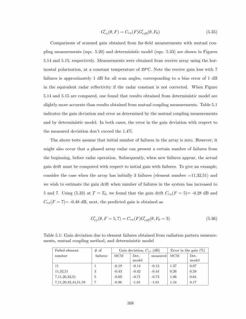
G′rx(θ, F ) = Crx(F )G′rx0(θ, F0) (5.35)
Comparisons of scanned gain obtained from far-field measurements with mutual cou-
pling measurements (equ. 5.20) and deterministic model (equ. 5.33) are shown in Figures
5.14 and 5.15, respectively. Measurements were obtained from receive array using the hor-
izontal polarization, at a constant temperature of 29oC. Note the receive gain loss with 7
failures is approximately 1 dB for all scan angles, corresponding to a bias error of 1 dB
in the equivalent radar reflectivity if the radar constant is not corrected. When Figure
5.14 and 5.15 are compared, one found that results obtained from deterministic model are
slightly more accurate than results obtained from mutual coupling measurements. Table 5.1
indicates the gain deviation and error as determined by the mutual coupling measurements
and by deterministic model. In both cases, the error in the gain deviation with respect to
the measured deviation don’t exceed the 1.4%.
The above tests assume that initial number of failures in the array is zero. However, it
might also occur that a phased array radar can present a certain number of failures from
the beginning, before radar operation. Subsequently, when new failures appear, the actual
gain drift must be computed with respect to initial gain with failures. To give an example,
consider the case when the array has initially 3 failures (element number =11,32,51) and
we wish to estimate the gain drift when number of failures in the system has increased to
5 and 7. Using (5.33) at T = T0, we found that the gain drift Crx(F = 5)= -0.28 dB and
Crx(F = 7)= -0.48 dB, next, the predicted gain is obtained as
G′rx(θ, F = 5, 7) = Crx(F )G′rx0(θ, F0 = 3) (5.36)
Table 5.1: Gain deviation due to element failures obtained from radiation pattern measure-ments, mutual coupling method, and deterministic model
Failed element # of Gain deviation, Crx (dB) Error in the gain (%)
number failures MCM Det.model
measured MCM Det.model
11 1 -0.19 -0.14 -0.13 1.37 0.07
11,32,51 3 -0.43 -0.42 -0.44 0.26 0.59
7,11,20,32,51 5 -0.69 -0.71 -0.73 1.06 0.64
7,11,20,32,44,51,59 7 -0.96 -1.01 -1.01 1.16 0.17
168

−50 −40 −30 −20 −10 0 10 20 30 40 50−4
−3.5
−3
−2.5
−2
−1.5
−1
−0.5
0
Scan angle (deg)
Nor
mal
ized
am
plitu
de (
dB)
Measured, F=0Measured, F=1Measured, F=3Measured, F=5Measured, F=7MCM, F=1MCM, F=3MCM, F=5MCM, F=7
Figure 5.14: Comparison of scanned gain under different failure condition, obtained byradiation pattern measurements and by prediction using mutual coupling measurements.
−50 −40 −30 −20 −10 0 10 20 30 40 50−4
−3.5
−3
−2.5
−2
−1.5
−1
−0.5
0
Scan angle (deg)
Nor
mal
ized
am
plitu
de (
dB)
Measured, F=0Measured, F=1Measured, F=3Measured, F=5Measured, F=7Det. Model, F=1Det. Model, F=3Det. Model, F=5Det. Model, F=7
Figure 5.15: Comparison of scanned gain under different failure condition, obtained byradiation pattern measurements and by prediction using deterministic model.
169

−50 −40 −30 −20 −10 0 10 20 30 40 50−3.5
−3
−2.5
−2
−1.5
−1
−0.5
0
Scan angle (deg)
Nor
mal
ized
am
plitu
de (
dB)
Measured, F=3Measured, F=5Measured, F=7Det. Model, F=5Det. Model, F=7
Figure 5.16: Comparison of scanned gain for the case of an array with initial failures,obtained by far-field radiation pattern and by prediction using deterministic model.
Figure 5.16 shows the scanned gain as determined by far-field measurements and by
prediction based on the deterministic model when the initial array has 3 failures and actual
array has 5 and 7 failures. We found again a very good match between the measured and
predicted gain. The result demonstrates that gain estimation must be based on the initial
number of failures, the number than can be found using mutual coupling measurements
after radar calibration.
Failures not only affect the gain of an array, it also increases the sidelobe in a radiation
pattern. Figure 5.17 shows how sidelobes are affected by the failed elements given in Table
5.1. The data corresponds to the maximum sidelobe, which can occur at any azimuth angle.
Note that a small number of failures produce a large change in the sidelobes. For example,
when the beam is at broadside, the sidelobe is raised from -24 dB to -19 dB, point where
the array has 3 failed elements. Because of the small number of elements in the array (64
elements), the sidelobes tends to increase rapidly after a few failures, something that does
not occur on a large phased array with thousand of elements.
170
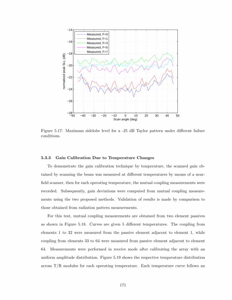
−50 −40 −30 −20 −10 0 10 20 30 40 50−28
−26
−24
−22
−20
−18
−16
−14
Scan angle (deg)
norm
aliz
ed p
eak
SLL
(dB
)
Measured, F=0Measured, F=1Measured, F=3Measured, F=5Measured, F=7
Figure 5.17: Maximum sidelobe level for a -25 dB Taylor pattern under different failureconditions.
5.3.3 Gain Calibration Due to Temperature Changes
To demonstrate the gain calibration technique by temperature, the scanned gain ob-
tained by scanning the beam was measured at different temperatures by means of a near-
field scanner, then for each operating temperature, the mutual coupling measurements were
recorded. Subsequently, gain deviations were computed from mutual coupling measure-
ments using the two proposed methods. Validation of results is made by comparison to
those obtained from radiation pattern measurements.
For this test, mutual coupling measurements are obtained from two element passives
as shown in Figure 5.18. Curves are given 5 different temperatures. The coupling from
elements 1 to 32 were measured from the passive element adjacent to element 1, while
coupling from elements 33 to 64 were measured from passive element adjacent to element
64. Measurements were performed in receive mode after calibrating the array with an
uniform amplitude distribution. Figure 5.19 shows the respective temperature distribution
across T/R modules for each operating temperature. Each temperature curve follows an
171

0 10 20 30 40 50 60 70−45
−40
−35
−30
−25
−20
−15
−10
−5
0
Element number
| Cn,
p | (d
B)
T
0 = 30.1° C
T1 = 32.9° C
T2 = 34.5° C
T3 = 42° C
T4 = 47° C
Figure 5.18: Mutual coupling measurements obtained at different operating temperaturesusing two passive elements.
uniform distribution with means T0=30.1 oC, T1=32.9 oC, T2=34.5 oC ,T3=42 oC, and
T4=47 oC, and mean standard deviation of 0.86 oC.
As described in section 5.2.2.1, the calibration uses the comparison of a previously
measured data with a reference data for detecting gain variations. In this test, we have
considered as the reference data, the measurements taken at temperature 30.1 oC. The
mutual coupling ratio Kn between the actual data (data at temperatures T1, T2, T3, and
T4) and reference data (data at temperature T0) as a function of element number is shown
in Figure 5.20. As expected, an increase in the T/R module temperature causes a decrease
in the gain of each element, reducing the intensity of mutual coupling between the active
and passive elements. The coupling reduction produces a negative shift in the parameter
Kn that is equal to the gain drift in each element.
Having obtained the parameter Kn, the subsequent gain drift at each temperature is
computed using (5.18) and (5.20). Additionally, the gain drift is computed by using the
deterministic model (5.33), after considering no failures in the array, and using αrx=0.007.
172

0 10 20 30 40 50 60 7026
28
30
32
34
36
38
40
42
44
46
Element number
Tem
pera
ture
(°
C)
T0
T1
T2
T3
T4
Figure 5.19: Temperature distribution along the T/R modules for different operating tem-peratures.
0 10 20 30 40 50 60 70−2.5
−2
−1.5
−1
−0.5
0
0.5
Element number
| K
n | (d
B)
−0.17−0.29
−0.70
−1.03
T1 = 32.9 °C
T2 = 34.5 °C
T3 = 42 °C
T4 = 47 °C
Figure 5.20: Gain deviation obtained at different operating temperatures using mutualcoupling technique.
173

The calibration constant for the receive array is given as
Crx[dB] = −0.0608(T − 30.1)
Results obtained from both methods were used to predict the array scanned gain at
each operating temperature. Comparisons of scanned gains obtained by mutual coupling
measurements and deterministic model with obtained by far-field radiation pattern mea-
surements are shown in Figure 5.21 and 5.22. In most cases, the predicted results are in
good agreement with measurements. While at temperature 47 oC there are some differences
at certain scan angles. These differences are caused by two reasons: the increase of random
errors in the excitation and by failures that occurs in some T/R modules. Failures in T/R
modules are caused by the thermal protection circuits in the voltage linear regulators that
feed the amplifiers. It has been observed specifically in 3 T/R modules that voltage reg-
ulator tends to cut-off the output current when temperatures reach values higher than 50
oC. Since the scanned gain measurement with the near-field scanner take about 40 minutes,
it is possible that affected modules can be switching between“on” and “off” states. Table
5.2 summaries the gain drift measured and computed by the two proposed methods, as
well as the errors obtained by each methods. The estimated errors are quite low, providing
evidence that both methods work very well to monitor the gain drift caused by temperature
changes.
Table 5.2: Gain deviation due to temperature changes
Initial Actual Gain deviation, Crx (dB) Error in the gain (%)
temperatureoC
temperatureoC
MCM Det.model
measured MCM Det.model
30.1 32.9 -0.17 -0.170 -0.15 0.20 0.21
30.1 34.5 -0.29 -0.27 -0.23 0.66 0.39
30.1 42 -0.72 -0.73 -0.67 0.60 0.68
30.1 47 -1.04 -1.03 -1.07 0.30 0.40
5.3.4 Gain Calibration Due to Temperature Changes and T/R Module Failures
The gain deviation due to temperature changes and failures was also investigated. The
test was realized at a temperature 41oC simulating 5 faulty elements (module numbers =
174

−50 −40 −30 −20 −10 0 10 20 30 40 50−4
−3.5
−3
−2.5
−2
−1.5
−1
−0.5
0
Scan angle (deg)
Nor
mal
ized
am
plitu
de (
dB)
T=30.1C (meas)T=32.9C (meas)T=34.5C (meas)T=42C (meas)T=47C (meas)T=32.9C (MCM)T=34.5C (MCM)T=42C (MCM)T=47C (MCM)
Figure 5.21: Scanned gain at different operating temperatures, obtained by radiation pat-tern measurements and by prediction using mutual coupling measurements.
−50 −40 −30 −20 −10 0 10 20 30 40 50−4
−3.5
−3
−2.5
−2
−1.5
−1
−0.5
0
Scan angle (deg)
Nor
mal
ized
am
plitu
de (
dB)
scanned gain variation versus temperature drift
T=30.1C (meas)T=32.9C (meas)T=34.5C (meas)T=42C (meas)T=47C (meas)T=32.9C (Det. model)T=34.5C Det. model)T=42C (Det. model)T=47C (Det. model)
Figure 5.22: Scanned gain at different operating temperatures, obtained by radiation pat-tern measurements and by prediction using deterministic model.
175

7, 11, 20, 32 and 51) in the array. It has been assumed as reference data, the data obtained
from an array operating with zero failures at temperature of 30.1 oC. For each temperature,
receive pattern measurements were made at 47 different scan angles in the range ±45o,
results were then used to estimate scanned gain in the scanning range. Subsequently, mutual
coupling measurements were made to estimate the gain drift and number of failures. Figure
5.23 shows the comparison of the initial scanned gain with actual scanned gain affected by
failure and temperature changes, as determined by measures and by prediction using the
two proposed methods. Results from this comparison are shown in Table 5.3. The measured
and predicted gain are matched fairly well over most of the scan range, the error obtained
from prediction using mutual coupling method and deterministic model are 0.2% and 0.6%,
respectively.
−50 −40 −30 −20 −10 0 10 20 30 40 50−4
−3.5
−3
−2.5
−2
−1.5
−1
−0.5
0
Scan angle (deg)
Sca
nned
gai
n
Measured (T0= 30.1 °C, F
0= 0)
Measured (T= 41 °C, F= 5)Det. model (T= 41 °C, F= 5)MCM (T= 41 °C, F= 5)
Figure 5.23: Effects of temperature and failures on the scanned gain. Curves obtainedby radiation pattern measurements, by prediction using mutual coupling method, and bydeterministic model.
176

Table 5.3: Gain deviation due to temperature changes and failed elements
Actual # of Gain deviation, Crx (dB) Error in the gain (%)temperatureoC
failures MCM Det.model
measured MCM Det.model
41 5 -1.40 -1.37 -1.35 0.2 0.6
177
CHAPTER 6
SUMMARY AND CONCLUSION
Benefits of dense networks of short-range X-band weather radars using mechanically
steered dishes has been recognized in the past 10 years. The need to improve radar capa-
bilities in order to provide early warning of hazardous weather phenomena, and the need
to provide more reliable and cost-effect radar systems have led to the consideration of us-
ing the phased array as an alternative technology to mechanically steered antennas. A
drawback of phased array systems are their high cost, making them too expensive for civil
application. For the concept of dense networks of phased array radar to be an economically
feasible alternative, the radar must be built at dramatically lower cost than current phased
array systems. A feasible solution is to use the phase-tilt array architecture, which performs
electronic scanning in azimuth direction and mechanical scanning in elevation direction.
The first part of this dissertation describes the design and implementation of a beam-
forming network and beam steering control system that enable the development of low-cost
low-power phase-tilt radars. A detailed, system-oriented description of the electrical re-
quirements, design, test, and performance of different subsystems were given.
A summary of the most important results and findings in this part of the dissertation
are as follows:
• The phase-tilt array architecture reduces cost because it uses a reduced number of
low-cost T/R modules in the array aperture. T/R modules make up about 50% of
overall system cost. Additionally, a significant cost reduction have been achieved in
the fabrication of other array subsystems by integrating in a single printed circuit
board (called backplane) the design of RF power distribution networks, DC power
network, control network. The cost has been reduced over other architectures through
increased integration of subsystems and reduced wiring, accounting for about 6% of
total array cost.
178

• T/R module design approach is based on radar system specifications and calibration
requirements. Modules are designed in individual boards to reduce maintenance cost
and provide low cost replacement parts. They also use their own housing to reduce
coupling between adjacent modules, which allows the investigation of mutual coupling
as calibration technique. The fabrication and assembly is realized in arrayed panels
to ensure low-cost manufacturing. The cost of each module is approximate $ 350
dollars (in year 2010) at high volume production. Within the module cost, the digital
phased shifter is the dominant factor, accounting for about 25% of current module
cost. Module test was very intense and time consuming. Measurements were realized
at an automated test station that was specifically designed for this project. The key
parameters, the transmit peak power, noise figure and the isolation between antenna
polarization ports met the design requirements. Additionally, the modules presented
a low settling time. Switch characteristics allows the phased array to theoretically
achieve pulse repetition frequencies up to 100 KHz, making it suitable for a wide
range of radar applications.
• Considerable simplification in the integration of various subsystems with T/R mod-
ules have been obtained by means of a hybrid backplane architecture, an interconnect
interface widely used in computer systems to make reliable and high speed connec-
tions between several daughter cards. The backplanes are composed of two RF power
distribution networks, a DC power network, and a control and communication bus.
These subsystems have been incorporated into a low-cost multilayer printed circuit
board. The board allows the interconnection of 16 T/R modules to a common com-
munication bus and power distribution system without using cables. T/R modules
are plugged into the backplane in their appropriate slots, according T/R module ad-
dress. The connection between T/R modules and RF manifold is realized through RF
coaxial cables. The advantages of using a backplane architecture is that it reduces
cost (i.e. reduce material and manufacturing process steps), reduce wiring complexity
and space, simplifies array integration, and allows the implementation of high-speed
communication buses.
179

• One of the most important results coming from the beam steering control design
was the implementation of a high-speed bus based on a LVDS multidrop backplane
architecture. The bus is capable of driving up to 32 T/R modules in parallel when
two backplanes are cascaded. It also allows data transmission speeds up to 100 Mbps.
The communication speed is 10 times higher than the communication speed obtained
in most phased arrays using RS485 and RS422 standards. Buses are designed with
a pair of microstrip lines and with terminations at the ends to eliminate reflections
caused by the mismatch between the transmission lines and loads. Tests made in a
heavily load backplane with 32 modules using a 25 Mbps serial transmission resulted
in a zero-error communication.
• A new control architecture for the beam steering system of a phased array radar was
designed and implemented. The control is based on a distributed system, which has a
central controller and several element controllers at the level of each T/R module. The
central controller generates beam commands and element controllers translate them
into calibrated settings allowing the implementation of the desired excitation. The
control differs from others architectures in that all element controllers are controlled in
parallel and synchronously by the central controller, and that non computing units are
used. In addition, element controllers can be controlled individually or simultaneously
by means of unicast or broadcast commands. Advantages of this architecture include
real time rapid update, high steering throughput, decreased complexity, and reduced
hardware cost. Some of these features enable the implementation of adaptive scan
and beam multiplexing scan strategy with a widely range of PRF and pulse width.
Another feature is that sequence table enables the implementation of a variety of
different pulse schemes.
• Element controllers are implemented in a low-cost small FPGA incorporated in the
T/R modules. The design is based on a state-machine with a programmable sequence
table and pre-stored calibration look-up table. The sequence table stores the beam
commands (scan angle + pulse scheme) to be used for the radar at a specific beam.
Look-up table translates the command indicated by the sequence table into control
180

signals for phase shifter, attenuator, T/R switches, polarizations switches and ampli-
fier bias. Each T/R module has a unique look-up table, which contains calibrated data
for different operation modes, temperature or even frequencies. Control of sequence
table, memory and registers is realized through commands. A list of commands with
their description have been presented.
The second study has addressed a method to perform the initial calibration of phased
arrays. The conventional method of setting the phase and amplitude in a phased array
system is through calibration look-up tables that are stored locally at each T/R module.
These tables store calibration offsets or calibrated settings that correct the errors created
by attenuators and phased shifters. This method does not always provide the best avail-
able setting for a given element excitation. The third chapter has addressed a calibration
algorithm that provides better calibration settings than the standard calibration. The algo-
rithm searches in the raw data of each element the best amplitude and phase settings that
minimize the random errors in the excitation. The settings are obtained as a function of
module, scan angle, and temperature. These data are organized and stored into calibration
tables, called ”beamtables”, in the array control computer, which transfers them to T/R
modules each time the radar is turned on or is in idle mode. Additionally, array radiation
patterns can be calculated from the calibration settings, the known array element positions,
and a known embedded element pattern.
A summary of the most important results and findings in this part of the dissertation
are as follows:
• The power of the calibration technique has been demonstrated by calibrating success-
fully a phased array system in both receive and transmit mode. The criteria used to
choose the gain scaling factor for the calibration algorithm at each mode depends on
the antenna operation mode. In receive, the gain scaling factor should be chosen less
than or equal to the minimum gain found across elements (having the attenuators and
phase shifters are loaded with all zeros) in order to implement the desired excitation
function with low random errors. This condition allows achievement of errors that
are approximately close to theoretical errors. On the other hand, in transmit, the
181

gain scaling factor should be chosen equal to the maximum gain found across the
elements. This condition ensures that elements will operate in compression. Results
have shown that when attenuator’s insertion phase is considered into the calibration,
a RMS phase error better than the theoretical error is obtained.
• Radiation pattern measurements obtained from calibrated array are in good agreement
with both theoretical and predicted patterns. Results indicate that radiation patterns
can be calculated directly from calibration settings if the embedded element pattern is
known. This method may be applicable to predict the radiation patterns of a fielded
phased array after internal calibration.
• Both measured and predicted patterns have been used to determine the array scanning
performance. Comparisons of scanned gains obtained by measurements, by prediction,
and by average embedded element pattern are made. It has been observed the presence
of ripples on the scanned gain in both receive and transmit array, being most noticeable
in receive than in transmit, although the latter had higher excitation errors. These
ripples are caused by the variation of amplitude errors with scan angles. Particularly,
in transmit there are not variations in the amplitude errors with scanning because the
elements operates in compression. For that reason, the ripples are quite small in the
scanned gain.
• Array characteristics as beamwidth, sidelobes, and beam pointing errors have been
measured are different scan angles in order to evaluate the quality of the calibration
process. The beamwidth performance is in good agreement with the theory. Sidelobe
level for beams close to broadside corresponds with the designed value, however its
value increases when the beam is scanned away from broadside because of the scanning
loss, being the maximum value equal to -21 dB at 45o. Beam pointing errors less than
0.06o has been obtained.
• An open loop calibration technique that compensates for the two-way antenna gain
drift caused by temperature changes is also presented. The technique is applicable
to phased arrays that have transmit modules operating in compression. Because the
gain cannot be adjusted in the transmit array, the compensation is realized in the
182

receive array. Gain compensation has been demonstrated experimentally at several
temperatures. Results show that the gain drift obtained after compensation is less
than 0.05 dB.
The third study has addressed a technique that uses mutual coupling measurements for
both monitoring and calibration of phase array systems. The technique takes advantage
of the inherent mutual coupling between the active elements and passive elements of an
array to measure the characteristics of active elements. The only two requirements of the
technique is that characteristics of passive elements and mutual coupling between radiating
elements must not change over time. It has been demonstrated successfully that mutual
coupling measurements can be used to monitor and maintain the calibration of an array.
In general, experiments has been conduced to estimate gain variations in the elements that
may be caused by temperature changes, aging, or even replaced modules. Results have been
used to calibrate the array elements when they suffers of excitation errors, and to calibrate
the radar constant when the array suffers of temperature and failures effects. The approach
has the advantage of low cost and easy implementation. The added circuit complexity is
also minimal.
A summary of the most important results and findings in this part of the dissertation
are as follows:
• The theory associated with monitoring and calibration of phased arrays that are sus-
ceptible to temperature changes has been discussed and demonstrated experimentally.
The calibration concept uses the comparison of two mutual coupling measurements,
one obtained during the monitoring task, the other one obtained during initial ar-
ray calibration, to determine calibration errors that occur in the elements over time.
It has been demonstrated that when two measurements are made at different tem-
peratures, the calibration constant is affected by a bias error that is exponentially
proportional to the temperature drift. The proposed calibration algorithm removes
the bias caused by the temperature and corrects the characteristics of uncalibrated
elements according to the calibration constant. Test results indicate that both gain
and phase drift can be calibrated with good accuracy if the signal-to-noise ratio is
183

the appropriated. Radiation pattern measurements confirmed that sidelobe level and
beamwidth are within the expected values after calibration procedure.
• The accuracy of the mutual coupling measurements are affected by the signal-to-noise
ratio resulting from the coupling between the active elements and passive elements,
as the separation distance increases, the signal-to-noise ratio decreases and accuracy
decreases. In a small linear phased array, the accuracy of calibration can be improved
by using two passive elements, one on each edge of the array, and measuring each half
of the antenna with the closer passive element.
• Results obtained by mutual coupling measurements can be used with the initial array
excitation function, and a known embedded element pattern to predict the array
radiation pattern. It has been shown that prediction results are in good agreement
with conventional far-field measurements. This method may prove to be very useful in
the maintenance of future low cost phased array radars where the radiation patterns
must be monitored routinely to insure that they meet the radar specifications. In
particular, small phased arrays are more susceptible to failures than large phased
array, the effect of failures is to reduce the antenna directivity and rise the sidelobes.
The antenna degradation can only be determined by measuring the antenna radiation
pattern. The pattern prediction by mutual coupling measurements can be a viable
alternative for performing this task.
• An experimental investigation of temperature and failures effects in an air-cooled,
phased array antenna has been made. It was shown that losses in receive gain can
be approximately 1 dB when the array has 7 failed modules. Similarly, the gain
deviation is 1 dB when the antenna is affected by a temperature change of 17 oC.
Combining both effects, the net gain deviation in receive can be equal to 2 dB. Unless
this deviation and transmit gain deviation is compensated, the equivalent reflectivity
measured by the radar will be affected by a bias error larger than 2 dB.
• The potential for radar calibration based on mutual coupling measurements has been
demonstrated. Two methods that effectively estimate the antenna gain deviation due
to temperature changes and failures are presented. The first method is based on the
184
comparison of the actual antenna gain with the initial antenna gain measured during
the external calibration of the radar. Each gain depends on the individual gains of
each array branch, which are obtained by mutual coupling measurements. The second
method is based on a mathematical model that takes into account the temperature
characteristic of T/R modules and the number of failures presents in the array. The
number of failures is estimated by mutual coupling measurements. The calibration
constants obtained from these methods correct the combined losses that occur in
the beamformer networks and antenna directivity. Two calibration constants, one
for transmit array and one for receive array, are defined to correct the radar system
constant. It was also shown that calibration constants can be used with the embedded
element pattern to predict the scanned gain of an array.
• Various calibration tests made under different operating temperatures and failures
conditions were shown. Results indicate that gain deviation can be accurately esti-
mated using any of the two proposed methods. Predicted scanned gains are in good
agreement with far-field measurements. Residual errors are less than 1.4 % in the
mutual coupling method and less than 0.7% in the mathematical model. Besides
accuracy, the mathematical model has the advantage that non mutual coupling mea-
surements are needed to calibrate the gain during radar operations. It is assumed that
calibration term due to failures is updated only after the array maintenance, when
there is not precipitation, while calibration term due to temperature should be up-
dated more often, for example, every scan sector after reading the temperature from
T/R modules.
• The calibration techniques based on mutual coupling measurements prove to be a vi-
able alternative to conventional techniques. Their accuracy, reduced cost and reduced
complexity makes them a good candidate for use in low-cost X-band phased array
radars.
185

APPENDIX A
T/R MODULE SCHEMATIC
This appendix provides the following circuit board schematics:
• RF circuit diagram
• Voltage regulators diagram
• Digital circuit and 30 pin header diagram
This appendix also includes the bill of material for T/R module
186

55
44
33
22
11
DD
CC
BB
AA
+5Va
-5Va
-5Va
-5Va
+3.3Va
+7Va
+5Va
-5Va
-5Va
-5Va-5Va
+5Va
+5Va
+5Va
-5Va
AGND
+5Va
+5Va
-5Va
+5Va
+5Va
AGND
AGND
AGND
AGND
AGND
AGND
AGND
AGND
AGND
AGND
AGND
AGND
AGND
AGND
AGND
AGND
AGND
AGND
AGND
AGND
AGND
AGND
AGND
AGND
AGND
AGND
AGND
AGND
AGND
AGND
AGND
AGND
AGND
AGND
AGND
AGND
AGND
AGND
AGND
AGND
AGND
AGND
AGND
AGND
AGND
AGND
AGND
AGND
AGND
AGND
AGND
AGND
AGND
AGND
AGND
AGND
AGND
AGND
AGND
AGND
AGND
AGND
AGND
AGND
AGND
AGND
AGND
AGND
AGND
AGND
AGND
AGND
AGND
AGND
AGND
AGND
AGND
AGND
AGND
AGND
AGND
AGND
AGND
AGND
AGND
AGND
AGND
AGND
AGND
AGND
AGND
AGND
AGND
AGND
AGND
AGND
AGND
AGND
AGND
AGND AGND
AGND
AGND
AGND
AGND
AGND
AGND
AGND
AGND
AGND
AGND
AGND
AGND
AGND
AGND
AGND
AGND +Vdd_GB
S1
+Vdd_MPA
+Vdd_PA
+Vdd_PA
Rx
Vdd_LNA
S1
Vdd_LNA
Rx
Vdd_LNA
+Vdd_PA
+Vdd_PA
+Vdd_MPA
+Vdd_GB
S2
S2
S1
Tx
Tx
+Vdd_PA
S2
+Vdd_PA
Rx
VCT
Tx
HCT
A1
A2
A3
A4
A5
A6
P2
P1
P6
P5
P4
P3
Title
Size
Document N
umber
Rev
Date:
Sheet
of
RF subsystem
v2
CASA T/R module
Custom
13
Tuesday, A
ugust 2
4, 2010
Title
Size
Document N
umber
Rev
Date:
Sheet
of
RF subsystem
v2
CASA T/R module
Custom
13
Tuesday, A
ugust 2
4, 2010
Title
Size
Document N
umber
Rev
Date:
Sheet
of
RF subsystem
v2
CASA T/R module
Custom
13
Tuesday, A
ugust 2
4, 2010
R14
127 Ohm
R14
127 Ohm
HMC441LP3
U5
HMC441LP3
U5
NC11
RFIN2
NC33
NC44
NC1212
RFOUT11
NC1010
NC99
NC16
16
VDD
15
NC14
14
NC13
13
NC5
5
VGG1
6
VGG2
7
NC8
8LOADSWT2
LOADSWT2
R2
1
VOUT1
2
VOUT2
3
VIN
4
CTL
5
R1
6
HMC425LP3
U6
HMC425LP3
U6
GND11
RFIN2
GND33
B64
GND1212
RFOUT11
GND1010
B19
NC16
16
VDD
15
NC14
14
NC13
13
B5
5
B4
6
B3
7
B2
8
R10
50 Ohm
R10
50 Ohm
D3
MPP4203
D3
MPP4203 SN74LVC2G14DCKR
U10A
SN74LVC2G14DCKR
U10A
5
1
2
6
R12
127 Ohm
R12
127 Ohm
C58
100pF
C58
100pF
R21
240
R21
240
C21
100pF
C21
100pF
HMC232LP4
U7
HMC232LP4
U7
NC11
NC22
GND33
RFC4
GND55
NC66
NC1818
NC1717
A16
B15
NC1414
NC1313
NC24
24
GND23
23
RF2
22
GND21
21
NC20
20
NC19
19
NC7
7GND8
8RF1
9GND10
10
NC11
11
NC12
12
SN74LVC2G14DCKR
U10B
SN74LVC2G14DCKR
U10B
34
5 2
R16
4.7K
R16
4.7K
C4
100pF
C4
100pF
C35
100pF
C35
100pF
R60
210
R60
210
R59
210
R59
210
C34
100pF
C34
100pF
C19
2.2uF
C19
2.2uF
C6
100pF
C6
100pF
C16
100pF
C16
100pF
C27
100pF
C27
100pF
R30
100 Ohm
R30
100 Ohm
R22
210
R22
210
J4J4
1
3
2
R9
240
R9
240
C14
100pF
C14
100pF
R19
240
R19
240
R20
210
R20
210
R11
50 Ohm
R11
50 Ohm
C26
100pF
C26
100pF
R17
4.7K
R17
4.7K
D12
CZRU52C5V1
D12
CZRU52C5V1
C1
100pF
C1
100pF
C5
100pF
C5
100pF
C38
100pF
C38
100pF
LOADSWT3
LOADSWT3
R2
1
VOUT1
2
VOUT2
3
VIN
4
CTL
5
R1
6
J3J3
1
3
2
C37
100pF
C37
100pF
R7
127 Ohm
R7
127 Ohm
HMC441LP3
U2
HMC441LP3
U2
NC1
1
RFIN
2
NC3
3
NC4
4
NC12
12
RFOUT
11
NC10
10
NC9
9
NC1616
VDD15
NC1414
NC1313
NC55
VGG16
VGG27
NC88
C7
100pF
C7
100pF
R31
2.4 Kohms
R31
2.4 Kohms
R27
1.5K
R27
1.5K
C25
100pF
C25
100pF
C15
100pF
C15
100pF
HMC564LC4
U9
HMC564LC4
U9
NC1
1GND2
2RFIN
3GND4
4NC5
5NC6
6
NC18
18
GND17
17
RFOUT
16
GND15
15
NC14
14
NC13
13
NC2424
VDD123
NC2222
NC2121
NC2020
VDD219
NC77
NC88
NC99
NC1010
NC1111
NC1212
C10
100pF
C10
100pF
HMC441LP3
U8
HMC441LP3
U8
NC1
1RFIN
2NC3
3NC4
4
NC12
12
RFOUT
11
NC10
10
NC9
9
NC1616
VDD15
NC1414
NC1313
NC55
VGG16
VGG27
NC88
D7
MPP4203
D7
MPP4203
D15
CZRU52C2
D15
CZRU52C2
D5
MPP4203
D5
MPP4203
C23
100pF
C23
100pF
C8
100pF
C8
100pF
C11
100pF
C11
100pF HMC591LP5
U3
HMC591LP5
U3
NC1
1
NC2
2
GND3
3
RFIN
4
GND5
5
NC6
6
NC7
7
NC8
8
NC24
24
NC23
23
GND22
22
RFOUT
21
GND20
20
NC19
19
NC18
18
NC17
17
VDD532
NC3131
NC3030
NC2929
VDD428
NC2727
NC2626
VDD325
VGG9
NC1010
NC1111
NC1212
VDD113
NC1414
NC1515
VDD216
EXB-E10P472J
RN2
EXB-E10P472J
RN2
R12
R23
R34
R45
R810
R79
R68
R57
VCC1
1VCC2
6
SN74LVC2G14DCKR
U11B
SN74LVC2G14DCKR
U11B
34
52
C24
100pF
C24
100pF
D11
CZRU52C5V1
D11
CZRU52C5V1
D9
MPP4203
D9
MPP4203
SN74LVC2G14DCKR
U12A
SN74LVC2G14DCKR
U12A
5
1
2
6
C22
0.01uF
C22
0.01uF
R15
4.7K
R15
4.7K
C9
100pF
C9
100pF
D13
CZRU52C2
D13
CZRU52C2
C18
100pF
C18
100pF
C57
100pF
C57
100pF
C2
100pF
C2
100pF
LOADSWT1
LOADSWT1
R2
1
VOUT1
2
VOUT2
3
VIN
4
CTL
5
R1
6
R23
240
R23
240
HMC642LC5
U4
HMC642LC5
U4
NC11
NC22
NC33
NC44
GND55
RFIN6
GND77
NC88
NC2424
NC2323
NC2222
NC2121
GND2020
RFOUT19
GND1818
NC1717
NC32
32
NC31
31
NC30
30
NC29
29
NC28
28
NC27
27
NC26
26
NC25
25
B6
9
B5
10
B4
11
VSS
12
B3
13
B2
14
B1
15
VDD
16
C28
100pF
C28
100pF
DPDT
S1
DPDT
S1
RX
1
TX
4V
2
H3
C16
A15
R119
A27
C28
R1210
C312
A311
R2119
A413
C414
R2220
R3122
R3221
R4117
R4218
A515
C516
C1036
A1035
R8139
A937
C938
R8240
C824
A823
R7131
A725
C726
R7232
R6134
R6233
R5130
R5229
A627
C628
D4
MPP4203
D4
MPP4203
C29
100pF
C29
100pF
R18
4.7K
R18
4.7K
SN74LVC2G14DCKR
U12B
SN74LVC2G14DCKR
U12B
3 4
52
D2
MPP4203
D2
MPP4203
J2J21
3
2
C20
100pF
C20
100pF
D8
MPP4203
D8
MPP4203
C17
100pF
C17
100pF
J1J11
3
2
C56
100pF
C56
100pF
C33
100pF
C33
100pF
R28
1.5K
R28
1.5KR8
127 Ohm
R8
127 Ohm
R13
240
R13
240
LOADSWT4
LOADSWT4
R2
1
VOUT1
2
VOUT2
3
VIN
4
CTL
5
R1
6
R25
240
R25
240
C3
100pF
C3
100pF
EXB-E10C472J
RN1
EXB-E10C472J
RN1
R12
R23
R34
R45
R810
R79
R68
R57
VCC1
1VCC2
6
SN74LVC2G14DCKR
U11A
SN74LVC2G14DCKR
U11A
5
1
2
6
D14
CZRU52C2
D14
CZRU52C2
D6
MPP4203
D6
MPP4203
C59
100pF
C59
100pF
HMC232LP4
U1
HMC232LP4
U1
NC11
NC22
GND33
RFC4
GND55
NC66
NC1818
NC1717
A16
B15
NC1414
NC1313
NC24
24
GND23
23
RF2
22
GND21
21
NC20
20
NC19
19
NC7
7
GND8
8
RF1
9
GND10
10
NC11
11
NC12
12
D16
CZRU52C2
D16
CZRU52C2
C36100pF
C36100pF
C32
100pF
C32
100pF
D10
MPP4203
D10
MPP4203
D1
MPP4203
D1
MPP4203
187

5 5
4 4
3 3
2 2
1 1
DD
CC
BB
AA
+5Va
+3
.3V
a
+1
0V
a+
7V
a+
3.3
Vd
+2
.5V
d
+1
.2V
d
+5
Vd
-10
Va
-5V
a
AG
ND
AG
ND
AG
ND
AG
ND
AG
ND
AG
ND
AG
ND
AG
ND
AG
ND
AG
ND
Titl
e
Siz
eD
ocu
men
t N
um
be
rR
ev
Da
te:
Sh
ee
to
f
Vo
ltag
e R
eg
ula
tors
- P
ow
er
Su
bsy
ste
mv2
CA
SA
T/R
Mod
ule
C
23
Th
urs
da
y, J
uly
29
, 2
01
0
Titl
e
Siz
eD
ocu
men
t N
um
be
rR
ev
Da
te:
Sh
ee
to
f
Vo
ltag
e R
eg
ula
tors
- P
ow
er
Su
bsy
ste
mv2
CA
SA
T/R
Mod
ule
C
23
Th
urs
da
y, J
uly
29
, 2
01
0
Titl
e
Siz
eD
ocu
men
t N
um
be
rR
ev
Da
te:
Sh
ee
to
f
Vo
ltag
e R
eg
ula
tors
- P
ow
er
Su
bsy
ste
mv2
CA
SA
T/R
Mod
ule
C
23
Th
urs
da
y, J
uly
29
, 2
01
0
AP
11
17
Y2
5L
U1
8AP
11
17
Y2
5L
U1
8
VIN
3V
OU
T2
ADJ1
R5
6
30
0 O
hm
R5
6
30
0 O
hm
C3
0
10
uF
C3
0
10
uF
C5
5
0.1
uF
C5
5
0.1
uF
R5
83
00
Oh
mR
58
30
0 O
hm
R5
5
10
0 O
hm
R5
5
10
0 O
hm
C4
1
10
uF
C4
1
10
uF
LM
33
7
U2
4
LM
33
7
U2
4
VIN
12
VIN
24
VO
UT
3
ADJ1
C3
9
10
uF
C3
9
10
uF
R3
3
48
7 O
hm
R3
3
48
7 O
hm
C5
4
10
uF
C5
4
10
uF
C4
0
10
uF
C4
0
10
uF
AP
11
17
Y3
3L
U1
7AP
11
17
Y3
3L
U1
7
VIN
3V
OU
T2
ADJ1
C1
3
1u
F
C1
3
1u
F
R3
21
00
Oh
mR
32
10
0 O
hm
C1
2
1u
F
C1
2
1u
F
LD
11
17
S1
2T
RU
19
LD
11
17
S1
2T
RU
19
VO
UT
24
ADJ1
VO
UT
12
VIN
3
C6
1
0.1
uF
C6
1
0.1
uF
AP
11
17
Y3
3L
U1
6AP
11
17
Y3
3L
U1
6
VIN
3V
OU
T2
ADJ1
LM
31
7D
CY
U1
4L
M31
7D
CY
U1
4
VO
UT
24
ADJ1
VO
UT
12
VIN
3
R5
71
00
Oh
mR
57
10
0 O
hm
C3
1
1u
F
C3
1
1u
F
LM
31
7D
CY
U1
5L
M31
7D
CY
U1
5
VO
UT
24
ADJ1
VO
UT
12
VIN
3
188

55
44
33
22
11
DD
CC
BB
AA
SPI-C
LK
SPI-C
LK
SPI-M
ISO
SPI-M
ISO
SPI-M
OSI
SPI-M
OSI
PROG_CT
SPI-C
S
SPI-C
S
XTAL_CLK
CLK_OE
XTAL_CLK
CLK0_p
CLK0_n
DGND
DTA1_p
DTA1_n
DGND
CLK1_p
CLK1_n
DGND
DGND
CLK2_p
CLK2_n
SPI-M
OSI
SPI-M
ISO
SPI-C
LK
SPI-C
S
PROG_CT
AGND
RST
DGND
AGND
AGND
LVDS1_p
LVDS1_n
LVDS2_p
LVDS2_n
LVDS3_p
LVDS3_n
LVDS4_p
LVDS4_n
LVDS0_n
LVDS0_p
CLK_OE
DTA1_n
DTA1_p
CLK1_n
CLK1_p
DTA2_n
DTA2_p
CLK2_n
CLK2_p
LVDS1_p
LVDS1_n
LVDS2_p
LVDS2_n
LVDS3_p
LVDS3_n
LVDS4_p
LVDS4_n
LVDS0_p
LVDS0_n
RST
DTA2_p
DTA2_n
CLK0_n
CLK0_p
SDA
SCL
DGND
DGND
SDA
SCL
+3.3Vd
+2.5Vd
+1.2Vd
+3.3Vd
+2.5Vd
+3.3Vd
+3.3Vd
+3.3Vd
+3.3Vd
+3.3Vd
+5Vd
-10Va
+10Va
+3.3Vd
+3.3Vd
+3.3Vd
AGND
Rx
Tx
HCT
VCT
P1
P2
P3
P4
P5
P6
A1
A2
A3
A4
A5
A6
Title
Size
Document N
umber
Rev
Date:
Sheet
of
FPGA and Digital S
ubsyste
mv2
CASA T/R Module
C
33
Thursd
ay, Ju
ly 29, 2
010
Title
Size
Document N
umber
Rev
Date:
Sheet
of
FPGA and Digital S
ubsyste
mv2
CASA T/R Module
C
33
Thursd
ay, Ju
ly 29, 2
010
Title
Size
Document N
umber
Rev
Date:
Sheet
of
FPGA and Digital S
ubsyste
mv2
CASA T/R Module
C
33
Thursd
ay, Ju
ly 29, 2
010
CLK0 (Latch signal), T/R
(CLKINn)
(CLKINp)
(DTAINn)
(DATINp)
(CLK2n)
(CLK2p)
(DTAOUTp)
(DTAOUTn)
(CLKOUTn)
(CLKOUTp)
(CLKINn)
(CLKINp)
(DTAINn)
(DATINp)
(CLK2n)
(CLK2p)
(DTAOUTp)
(DTAOUTn)
(CLKOUTn)
(CLKOUTp)
R39
49.9
R39
49.9
R52
100 Ohm (1
40)
R52
100 Ohm (1
40)
C60
0.01uF
C60
0.01uF
C42
100nF
C42
100nF
ASE-25.000MHZ-LC-T
U22
ASE-25.000MHZ-LC-T
U22
OE
1
GND
2OUT
3
VDD
4
C63
100nF
C63
100nF
R24
4.7K
R24
4.7K
R5
4.7K
R5
4.7K
R49
100 Ohm (1
40)
R49
100 Ohm (1
40)
R3
4.7K
R3
4.7K
C64
100nF
C64
100nF
XC3S100E-4VQG100C
U20
XC3S100E-4VQG100C
U20
PROG_B
1
IO_L01P_2/CSO_B
24
IO_L01N_2/IN
IT_B
25
IO_L02P_2/DOUT/BUSY
26
IO_L02N_2/MOSI/C
SI_B
27
IO/D5
34
IO/M1
42
IO_L07P_2/M0
43
IO_L07N_2/DIN/D0
44
IO_L08P_2/VS2
47
IO_L08N_2/VS1
48
IO_L09P_2/VS0
49
IO_L09N_2/CCLK
50
DONE
51
TMS
75
TDO
76
TCK
77
IO_L07N_0/HSWAP
99
TDI
100
IO_L01P_3
2
IO_L01N_3
3
IO_L02P_3
4
IO_L02N_3/VREF_3
5
IO_L03P_3/LHCLK0
9
IO_L03N_3/LHCLK1
10
IO_L04P_3/LHCLK2
11
IO_L04N_3/LHCLK3/IR
DY2
12
IP13
IO_L05P_3/LHCLK4/TRDY2
15
IO_L05N_3/LHCLK5
16
IO_L06P_3/LHCLK6
17
IO_L06N_3/LHCLK7
18
IO_L07P_3
22
IO_L07N_3
23
IP/VREF_2
30
IO_L03P_2/D7/GCLK12
32
IO_L03N_2/D6/GCLK13
33
IO_L04P_2/D4/GCLK14
35
IO_L04N_2/D3/GCLK15
36
IP_L05P_2/RDWR_B/GCLK0
38
IP_L05N_2/M2/GCLK1
39
IO_L06P_2/D2/GCLK2
40
IO_L06N_2/D1/GCLK3
41
IO_L01P_1
53
IO_L01N_1
54
IO_L02P_1
57
IO_L02N_1
58
IO_L03P_1/RHCLK0
60
IO_L03N_1/RHCLK1
61
IO_L04P_1/RHCLK2
62
IO_L04N_1/RHCLK3/TRDY1
63
IO_L05P_1/RHCLK4/IR
DY1
65
IO_L05N_1/RHCLK5
66
IO_L06P_1/RHCLK6
67
IO_L06N_1/RHCLK7
68
IP/VREF_1
69
IO_L07P_1
70
IO_L07N_1
71
IO_L01P_0
78
IO_L01N_0
79
IO_L02P_0/GCLK4
83
IO_L02N_0/GCLK5
84
IO_L03P_0/GCLK6
85
IO_L03N_0/GCLK7
86
IP_L04P_0/GCLK8
88
IP_L04N_0/GCLK9
89
IO_L05P_0/GCLK10
90
IO_L05N_0/GCLK11
91
IO92
IO_L06P_0
94
IO_L06N_0/VREF_0
95
IO_L07P_0
98
VCCINT6
VCCO_38
VCCO_320
VCCAUX21
VCCINT28
VCCO_231
VCCO_245
VCCAUX46
VCCO_155
VCCINT56
VCCO_173
VCCAUX74
VCCINT80
VCCO_082
VCCAUX96
VCCO_097
GND7
GND14
GND19
GND29
GND37
GND52
GND59
GND64
GND72
GND81
GND87
GND93
R42
100 Ohm (1
40)
R42
100 Ohm (1
40)
R6
4.7K
R6
4.7K
R46
100 Ohm (1
40)
R46
100 Ohm (1
40)
R40
49.9 (1
65)
R40
49.9 (1
65)
C65
100nF
C65
100nF
R43100 Ohm (1
40)
R43100 Ohm (1
40)
R50
49.9 (1
65)
R50
49.9 (1
65)
C44
100nF
C44
100nF
C45
100nF
C45
100nF
C46
100nF
C46
100nF
C47
100nF
C47
100nF
C48
100nF
C48
100nF
C49
100nF
C49
100nF
R35
4.7K
R35
4.7K
C50
100nF
C50
100nF
SHORT
U25
SHORT
U25
T1
1T2
2
C51
100nF
C51
100nF
C52
100nF
C52
100nF
C53
100nF
C53
100nF
R47
49.9 (1
65)
R47
49.9 (1
65)
R29
4.7K
R29
4.7K
R51
49.9 (1
65)
R51
49.9 (1
65)
R44
49.9 (1
65)
R44
49.9 (1
65)
R2
4.7K
R2
4.7K
R37
4.7K
R37
4.7K
R48
49.9 (1
65)
R48
49.9 (1
65)
R53
2.4 Kohms
R53
2.4 Kohms
R34
4.7K
R34
4.7K
R26
4.7K
R26
4.7K
R54
2.4 Kohms
R54
2.4 Kohms
J5
HEADER 15X2
J5
HEADER 15X2
24681012141618202224262830
1357911131517192123252729
R45
49.9 (1
65)
R45
49.9 (1
65)
TC74
U23
TC74
U23
NC
1
GND
2
VDD
3
SDA
5
SCL
4
R4
4.7K
R4
4.7K
M25PE10
U21
M25PE10
U21
nS
1
Q2
nW
3
GND
4D
5C
6nR
7VCC
8
R36
4.7K
R36
4.7K
R38
49.9
R38
49.9
R41
49.9 (1
65)
R41
49.9 (1
65)
C43
100nF
C43
100nF
C62
100nF
C62
100nF
R1
4.7K
R1
4.7K
189

R
evis
ed: W
ednesday, M
arc
h 2
5, 2009
R
evis
ion:
v2
Bill
Of M
ate
rials
M
arc
h 2
5,2
009 14:0
5:2
0P
age1
Item
Quantity
Refe
rence
Valu
eP
art
Num
ber
Description
Dis
trib
uto
rD
ist P
art
Num
ber
______________________________________________
136
C1,C
2,C
3,C
4,C
5,C
6,C
7,C
8,C
9,C
10,C
11,C
14,C
15,C
16,C
17,C
18,C
20,C
21,C
23,
100pF
EC
J-0
EB
1E
682K
CA
P 1
00P
F 2
5V
CE
RA
MIC
X7R
0402
Dig
i-K
ey
PC
C1702C
T-N
D
C24,C
25,C
26,C
27,C
28,C
29,C
32,C
33,C
34,C
35,C
36,C
37,C
38,C
56,C
57,C
58,C
59
22
C12,C
31
1uF
TC
A1C
105M
8R
CA
P T
AN
T 1
UF
16V
20%
SM
DD
igi-K
ey
511-1
466-1
-ND
31
C13
1uF
TC
A1C
106M
8R
CA
P T
AN
T 1
0U
F 1
6V
20%
SM
DD
igi-K
ey
511-1
473-1
-ND
41
C19
2.2
uF
TC
A1C
225M
8R
CA
P T
AN
TA
LU
M 2
.2U
F 1
6V
20%
, 1206 S
MD
Dig
i-K
ey
511-1
469-1
-ND
52
C22,C
60
0.0
1uF
EC
J-1
VB
1E
103K
CA
P 1
0000P
F 2
5V
CE
RM
X7R
0603
Dig
i-K
ey
PC
C1763C
T-N
D
65
C30,C
39,C
40,C
41,C
54
10uF
TC
A1C
106M
8R
CA
P T
AN
T 1
0U
F 1
6V
20%
SM
DD
igi-K
ey
511-1
473-1
-ND
716
C42,C
43,C
44,C
45,C
46,C
47,C
48,C
49,C
50,C
51,C
52,C
53,C
62,C
63,C
64,C
65
100nF
EC
J-0
EB
1A
104K
CA
P .1U
F 1
0V
CE
RA
MIC
X5R
0402
Dig
i-K
ey
PC
C2146C
T-N
D
82
C55,C
61
0.1
uF
F971V
104M
AA
CA
P T
AN
TA
LU
M 0
.1U
F 3
5V
20%
SM
DD
igi-K
ey
493-2
431-1
-ND
92
D11,D
12
CZ
RU
52C
5V
1C
ZR
U52C
5V
1D
IOD
E Z
EN
ER
150M
W 5
.1V
0603
Dig
i-K
ey
641-1
029-1
-ND
10
4D
13,D
14,D
15,D
16
CZ
RU
52C
2C
ZR
U52C
2D
IOD
E Z
EN
ER
150M
W 2
V 0
603
Dig
i-K
ey
641-1
019-1
-ND
11
2J1,J
2S
MA
142-0
761-8
51
CO
NN
JA
CK
SM
A 5
0 O
HM
S P
C M
OU
NT
Dig
i-K
ey
J800-N
D
12
1J5
HE
AD
ER
15X
2T
FM
L-1
15-0
1-S
-D-R
AC
ON
N H
EA
DR
.05"
30P
OS
DL T
/H R
/AD
igi-K
ey
SA
M8263-N
D
13
1R
N1
EX
B-E
10C
472J
EX
B-E
10C
472J
RE
S N
ET
WR
K 4
.7K
OH
M 8
RE
S10P
N S
MD
Dig
i-K
ey
U8472C
T-N
D
14
1R
N2
EX
B-E
10P
472J
EX
B-E
10P
472J
RE
S N
ET
WR
K 4
.7K
OH
M 8
RE
S10P
N S
MD
Dig
i-K
ey
U8472C
T-N
D
15
13
R1,R
2,R
3,R
4,R
5,R
6,R
24,R
26,R
29,R
34,R
35,R
36,R
37
4.7
KE
RJ-2
GE
J472X
RE
S 4
.7K
OH
M 1
/10W
5%
0402 S
MD
Dig
i-K
ey
P4.7
KJC
T-N
D
16
4R
7,R
8,R
12,R
14
127 O
hm
RC
1206F
R-0
7127R
LR
ES
127 O
HM
1/4
W 1
% 1
206 S
MD
Dig
i-K
ey
311-1
27F
RC
T-N
D
17
5R
9,R
13,R
19,R
21,R
25
200
ES
R03E
ZP
J241
RE
S 2
00 O
HM
1/5
W 5
% 0
603 S
MD
Dig
i-K
ey
RH
M240D
CT
-ND
18
4R
15,R
16,R
17,R
18
4.7
KE
RJ-2
GE
J472X
RE
S 4
.7K
OH
M 1
/10W
5%
0603 S
MD
Dig
i-K
ey
P4.7
KJC
T-N
D
19
4R
20,R
22,R
59,R
60
210
ER
J-2
RK
F2100X
RE
S 2
10 O
HM
1/1
6W
1%
0402 S
MD
Dig
i-K
ey
P210LC
T-N
D
20
1R
23
200
ER
J-P
06J201V
RE
S 2
00 O
HM
1/4
W 5
% 0
805 S
MD
Dig
i-K
ey
P200A
DC
T-N
D
21
2R
27,R
28
1.5
KE
RJ-2
GE
J152X
RE
S 1
.5K
OH
M 1
/10W
5%
0603 S
MD
Dig
i-K
ey
P1.5
KJC
T-N
D
22
1R
30
100 O
hm
MC
R01M
ZP
J101
RE
S 1
00 O
HM
1/1
6W
5%
0402 S
MD
Dig
i-K
ey
RH
M100JC
T-N
D
23
3R
31,R
53,R
54
2.4
Kohm
sE
RJ-3
GE
YJ242V
RE
S 2
.4K
OH
M 1
/10W
5%
0603 S
MD
Dig
i-K
ey
P2.4
KG
CT
-ND
24
3R
32,R
55,R
57
100 O
hm
ER
J-3
GE
YJ101V
RE
S 1
00 O
HM
1/1
0W
5%
0603 S
MD
Dig
i-K
ey
P100G
CT
-ND
25
1R
33
487 O
hm
ER
J-3
EK
F4870V
RE
S 4
64 O
HM
1/1
0W
5%
0603 S
MD
Dig
i-K
ey
P487H
CT
-ND
26
2R
38,R
39
49.9
Ohm
ER
J-2
RK
F49R
9X
RE
S 4
9.9
OH
M 1
/16W
1%
0402 S
MD
Dig
i-K
ey
P49.9
LC
T-N
D
27
8R
40,R
41,R
44,R
45,R
47,R
48,R
50,R
51
49.9
Ohm
ER
J-2
RK
F49R
9X
RE
S 4
9.9
OH
M 1
/16W
1%
0402 S
MD
Dig
i-K
ey
P49.9
LC
T-N
D
28
5R
42,R
43,R
46,R
49,R
52
100 O
hm
MC
R01M
ZP
J101
RE
S 1
00 O
HM
1/1
6W
5%
0402 S
MD
Dig
i-K
ey
RH
M100JC
T-N
DN
o c
onnect
29
2R
56,R
58
300 O
hm
ER
J-3
GE
YJ301V
RE
S 3
00 O
HM
1/1
0W
5%
0603 S
MD
Dig
i-K
ey
P300G
CT
-ND
30
4T
1,T
2,T
3,T
4LO
AD
SW
FD
C6331L
Inte
gra
ted L
oad S
witch
Dig
i-K
ey
FD
C6331LC
T-N
D
31
3U
10,U
11,U
12
SN
74LV
C2G
14D
CK
RS
N74LV
C2G
14D
CK
RIC
IN
VE
RT
ER
DU
AL
Dig
i-K
ey
296-1
3011-1
-ND
32
2U
14,U
15
LM
317D
CY
LM
317D
CY
RIC
VO
LT
RE
G P
OS
AD
J S
OT
-223-4
Dig
i-K
ey
296-1
2602-1
-ND
33
2U
16,U
17
AP
1117Y
33L
AP
1117Y
33L
IC R
EG
LD
O 1
.0A
3.3
V S
OT
89-3
LD
igi-K
ey
AP
1117Y
33LD
ICT
-ND
34
1U
18
AP
1117Y
25L
AP
1117Y
25L
IC R
EG
LD
O 1
.0A
2.5
V S
OT
89-3
LD
igi-K
ey
AP
1117Y
25LD
ICT
-ND
35
1U
19
LD
1117S
12T
RLD
1117S
12T
RIC
RE
G L
DO
PO
S 8
00M
A 1
.2V
SO
T223
Dig
i-K
ey
497-4
240-2
-ND
36
1U
20
XC
3S
100E
-4V
QG
100C
XC
3S
100E
-4V
QG
100C
IC S
PA
RT
AN
-3E
FP
GA
100K
100V
TQ
FP
Dig
i-K
ey
122-1
479-N
D
37
1U
21
M25P
E10
M25P
E10-V
MN
6P
IC S
ER
IAL F
LA
SH
1M
BIT
LV
SO
-8N
Dig
i-K
ey
M25P
E10-V
MN
6P
-ND
38
1U
22
AS
E-2
5.0
00M
HZ
-LC
-TA
SE
-25.0
00M
HZ
-LC
-TO
SC
ILLA
TO
R 2
5.0
00 M
HZ
3.3
V S
MD
Dig
i-K
ey
535-9
568-1
-ND
39
1U
23
TC
74
TC
74A
0-5
.0V
CT
TR
IC D
GT
L T
HE
RM
SE
NS
OR
Dig
i-K
ey
TC
74A
0-5
.0V
CT
CT
-ND
40
1U
24
LM
337
LM
337IM
P/N
OP
BIC
VR
EG
NE
GA
TIV
E A
DJ 1
A S
OT
223
Dig
i-K
ey
LM
337IM
PC
T-N
D
910
D1,D
2,D
3,D
4,D
5,D
6,D
7,D
8,D
9,D
10
MP
P4203
MP
P4203
SM
PIN
dio
de
Mic
rosem
iM
PP
4203
13
2J3,J
4S
MP
P606-6
CC
CO
NN
JA
CK
SM
A 5
0 O
HM
S P
C M
OU
NT
Tensolit
eP
606-6
CC
20
2R
10,R
11
50 O
hm
RC
3-0
402P
W50R
0J
RE
S 5
0 O
HM
1/1
6W
1%
0402 S
MD
IMS
-Resis
tor
RC
3-0
402P
W50R
0J
35
2U
1,U
7H
MC
232LP
4H
MC
232LP
4G
aA
s M
MIC
SP
DT
Non-R
eflective S
witch
Hittite
HM
C232LP
4
36
3U
2,U
5,U
8H
MC
441LP
3H
MC
441LP
3G
aA
s M
MIC
Mediu
m p
ow
er
Am
plif
ier
Hittite
HM
C441LP
3
37
1U
3H
MC
591LP
5H
MC
591LP
5G
aA
s M
MIC
Pow
er
Am
plif
ier
Hittite
HM
C591LP
5
38
1U
4H
MC
642LC
5H
MC
642LC
5G
aA
s M
MIC
6-B
it D
igital P
hase S
hifte
rH
ittite
HM
C642LC
5
39
1U
6H
MC
425LP
3H
MC
425LP
3G
aA
s M
MIC
6-B
it D
igital A
ttenuato
rH
ittite
HM
C425LP
3
40
1U
9H
MC
564LC
4H
MC
564LC
4G
aA
S M
MIC
Low
Nois
e A
mplif
ier
Hittite
HM
C564LC
4
190
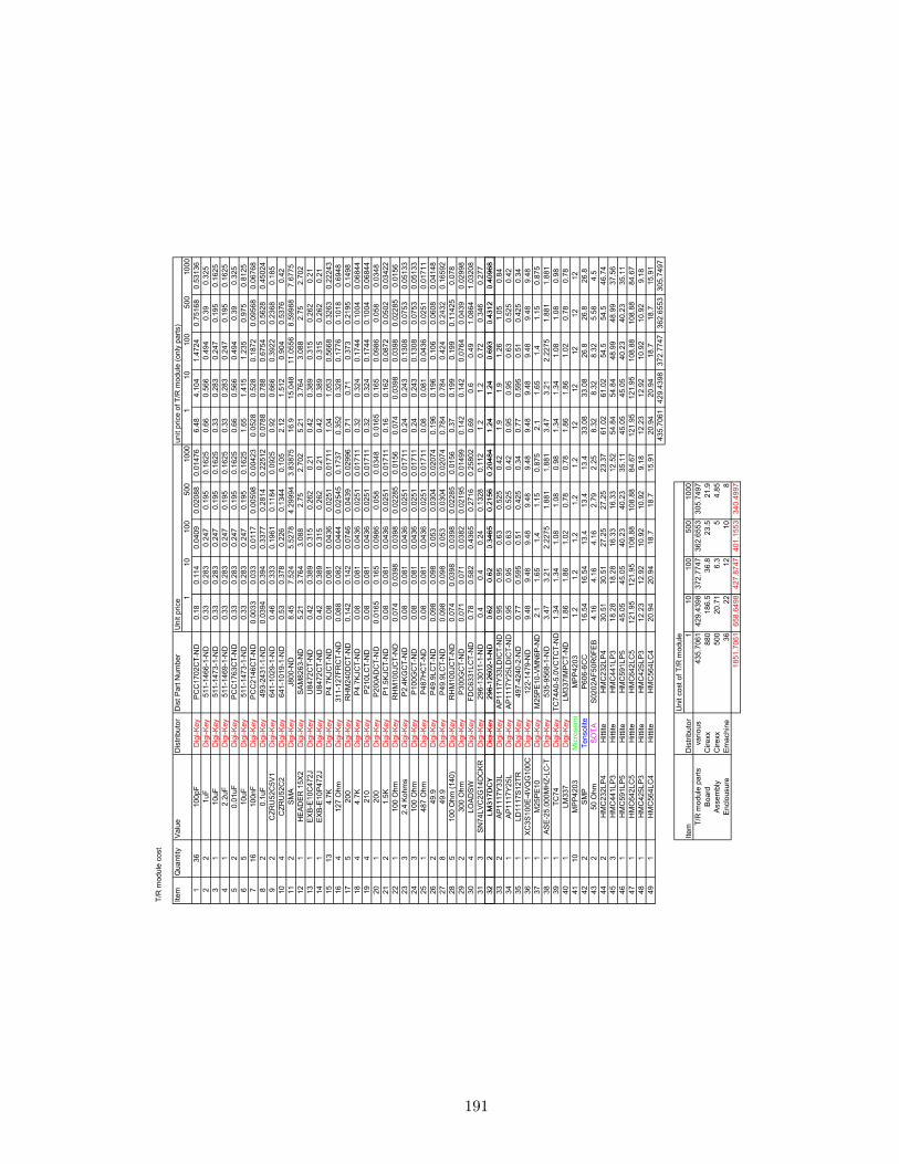
T/R module cost
Item
Quantity
Value
Distributor
Dist Part Number
Unit price
unit price of T/R module (only parts)
110
100
500
1000
110
100
500
1000
136
100pF
Digi-Key
PCC1702CT-ND
0.18
0.114
0.0409
0.02088
0.01476
6.48
4.104
1.4724
0.75168
0.53136
22
1uF
Digi-Key
511-1466-1-ND
0.33
0.283
0.247
0.195
0.1625
0.66
0.566
0.494
0.39
0.325
31
10uF
Digi-Key
511-1473-1-ND
0.33
0.283
0.247
0.195
0.1625
0.33
0.283
0.247
0.195
0.1625
41
2.2uF
Digi-Key
511-1469-1-ND
0.33
0.283
0.247
0.195
0.1625
0.33
0.283
0.247
0.195
0.1625
52
0.01uF
Digi-Key
PCC1763CT-ND
0.33
0.283
0.247
0.195
0.1625
0.66
0.566
0.494
0.39
0.325
65
10uF
Digi-Key
511-1473-1-ND
0.33
0.283
0.247
0.195
0.1625
1.65
1.415
1.235
0.975
0.8125
716
100nF
Digi-Key
PCC2146CT-ND
0.0033
0.033
0.0117
0.00598
0.00423
0.0528
0.528
0.1872
0.09568
0.06768
82
0.1uF
Digi-Key
493-2431-1-ND
0.0394
0.394
0.3377
0.2814
0.22512
0.0788
0.788
0.6754
0.5628
0.45024
92
CZRU52C5V1
Digi-Key
641-1029-1-ND
0.46
0.333
0.1961
0.1184
0.0925
0.92
0.666
0.3922
0.2368
0.185
10
4CZRU52C2
Digi-Key
641-1019-1-ND
0.53
0.378
0.226
0.1344
0.105
2.12
1.512
0.904
0.5376
0.42
11
2SMA
Digi-Key
J800-ND
8.45
7.524
5.5278
4.29994
3.83875
16.9
15.048
11.0556
8.59988
7.6775
12
1HEADER 15X2
Digi-Key
SAM8263-ND
5.21
3.764
3.088
2.75
2.702
5.21
3.764
3.088
2.75
2.702
13
1EXB-E10C472J
Digi-Key
U8472CT-ND
0.42
0.389
0.315
0.262
0.21
0.42
0.389
0.315
0.262
0.21
14
1EXB-E10P472J
Digi-Key
U8472CT-ND
0.42
0.389
0.315
0.262
0.21
0.42
0.389
0.315
0.262
0.21
15
13
4.7K
Digi-Key
P4.7KJCT-ND
0.08
0.081
0.0436
0.0251
0.01711
1.04
1.053
0.5668
0.3263
0.22243
16
4127 Ohm
Digi-Key
311-127FRCT-ND
0.088
0.082
0.0444
0.02545
0.1737
0.352
0.328
0.1776
0.1018
0.6948
17
5200
Digi-Key
RHM240DCT-ND
0.142
0.142
0.0746
0.0439
0.02996
0.71
0.71
0.373
0.2195
0.1498
18
44.7K
Digi-Key
P4.7KJCT-ND
0.08
0.081
0.0436
0.0251
0.01711
0.32
0.324
0.1744
0.1004
0.06844
19
4210
Digi-Key
P210LCT-ND
0.08
0.081
0.0436
0.0251
0.01711
0.32
0.324
0.1744
0.1004
0.06844
20
1200
Digi-Key
P200ADCT-ND
0.0165
0.165
0.0986
0.058
0.0348
0.0165
0.165
0.0986
0.058
0.0348
21
21.5K
Digi-Key
P1.5KJCT-ND
0.08
0.081
0.0436
0.0251
0.01711
0.16
0.162
0.0872
0.0502
0.03422
22
1100 Ohm
Digi-Key
RHM100JCT-ND
0.074
0.0398
0.0398
0.02285
0.0156
0.074
0.0398
0.0398
0.02285
0.0156
23
32.4 Kohms
Digi-Key
P2.4KGCT-ND
0.08
0.081
0.0436
0.0251
0.01711
0.24
0.243
0.1308
0.0753
0.05133
24
3100 Ohm
Digi-Key
P100GCT-ND
0.08
0.081
0.0436
0.0251
0.01711
0.24
0.243
0.1308
0.0753
0.05133
25
1487 Ohm
Digi-Key
P487HCT-ND
0.08
0.081
0.0436
0.0251
0.01711
0.08
0.081
0.0436
0.0251
0.01711
26
249.9
Digi-Key
P49.9LCT-ND
0.098
0.098
0.053
0.0304
0.02074
0.196
0.196
0.106
0.0608
0.04148
27
849.9
Digi-Key
P49.9LCT-ND
0.098
0.098
0.053
0.0304
0.02074
0.784
0.784
0.424
0.2432
0.16592
28
5100 Ohm (140)
Digi-Key
RHM100JCT-ND
0.074
0.0398
0.0398
0.02285
0.0156
0.37
0.199
0.199
0.11425
0.078
29
2300 Ohm
Digi-Key
P300GCT-ND
0.071
0.071
0.0382
0.02195
0.01499
0.142
0.142
0.0764
0.0439
0.02998
30
4LOADSW
Digi-Key
FDC6331LCT-ND
0.78
0.582
0.4365
0.2716
0.25802
0.69
0.6
0.49
1.0864
1.03208
31
3SN74LVC2G14DCKR
Digi-Key
296-13011-1-ND
0.4
0.4
0.24
0.1328
0.112
1.2
1.2
0.72
0.346
0.277
32
2LM317DCY
Digi-Key
296-12602-1-ND
0.62
0.62
0.3465
0.2156
0.20484
1.24
1.24
0.693
0.4312
0.40968
32
2LM317DCY
Digi-Key
296-12602-1-ND
0.62
0.62
0.3465
0.2156
0.20484
1.24
1.24
0.693
0.4312
0.40968
33
2AP1117Y33L
Digi-Key
AP1117Y33LDICT-ND
0.95
0.95
0.63
0.525
0.42
1.9
1.9
1.26
1.05
0.84
34
1AP1117Y25L
Digi-Key
AP1117Y25LDICT-ND
0.95
0.95
0.63
0.525
0.42
0.95
0.95
0.63
0.525
0.42
35
1LD1117S12TR
Digi-Key
497-4240-2-ND
0.77
0.595
0.51
0.425
0.34
0.77
0.595
0.51
0.425
0.34
36
1XC3S100E-4VQG100C
Digi-Key
122-1479-ND
9.48
9.48
9.48
9.48
9.48
9.48
9.48
9.48
9.48
9.48
37
1M25PE10
Digi-Key
M25PE10-VMN6P-ND
2.1
1.65
1.4
1.15
0.875
2.1
1.65
1.4
1.15
0.875
38
1ASE-25.000MHZ-LC-T
Digi-Key
535-9568-1-ND
3.47
3.21
2.2275
1.881
1.881
3.47
3.21
2.2275
1.881
1.881
39
1TC74
Digi-Key
TC74A0-5.0VCTCT-ND
1.34
1.34
1.08
1.08
0.98
1.34
1.34
1.08
1.08
0.98
40
1LM337
Digi-Key
LM337IMPCT-ND
1.86
1.86
1.02
0.78
0.78
1.86
1.86
1.02
0.78
0.78
41
10
MPP4203
Microsemi
MPP4203
1.2
1.2
1.2
1.2
1.2
12
12
12
12
12
42
2SMP
Tensolite
P606-6CC
16.54
16.54
13.4
13.4
13.4
33.08
33.08
26.8
26.8
26.8
43
250 Ohm
SOTA
S0202AF50R0FEB
4.16
4.16
4.16
2.79
2.25
8.32
8.32
8.32
5.58
4.5
44
2HMC232LP4
Hittite
HMC232LP4
30.51
30.51
27.25
27.25
23.37
61.02
61.02
54.5
54.5
46.74
45
3HMC441LP3
Hittite
HMC441LP3
18.28
18.28
16.33
16.33
12.52
54.84
54.84
48.99
48.99
37.56
46
1HMC591LP5
Hittite
HMC591LP5
45.05
45.05
40.23
40.23
35.11
45.05
45.05
40.23
40.23
35.11
47
1HMC642LC5
Hittite
HMC642LC5
121.95
121.95
108.88
108.88
84.67
121.95
121.95
108.88
108.88
84.67
48
1HMC425LP3
Hittite
HMC425LP3
12.23
12.92
10.92
10.92
9.18
12.23
12.92
10.92
10.92
9.18
49
1HMC564LC4
Hittite
HMC564LC4
20.94
20.94
18.7
18.7
15.91
20.94
20.94
18.7
18.7
15.91
435.7061
429.4398
372.7747
362.6553
305.7497
Unit cost of T/R module
Item
Distributor
110
100
500
1000
T/R module parts
various
435.7061
429.4398
372.7747
362.6553
305.7497
Board
Cirexx
880
186.5
36.8
23.5
21.9
Assembly
Cirexx
500
20.71
6.3
54.85
Enclousure
Emachine
36
22
12
10
8
1851.7061
658.6498
427.8747
401.1553
340.4997
191

APPENDIX B
BACKPLANE
This appendix provides the bill of material and cost model for the backplane board.
B.1 Bill of material
Item Quantity Part Part Number Description Distributor Dist Part Number Package Type
1 8 10A01-T 10A01-T RECTIFIER 50V 10A R-6 Digi-Key 10A01CT-ND R-6 Through-holes
2 18 SOCKET 15X2 SFML-115-T1-S-D CONN HEADR .05" 30POS DL T/H R/A Digi-Key SAM8243-ND CONN30SCK Through-holes
3 34 SMA 142-0711-201 CONN JACK SMA 50 OHMS PC MOUNT Digi-Key J819-ND SMA conn Surface Mount
4 1 HEADER 12POS 10-84-4120 MALE CONN HEADER 12POS .084 VERT TIN Digi-Key WM1261-ND CONN12 Through-holes
5 1 HEADER 6POS 10-84-4060 MALE CONN HEADER 6POS .084 VERT TIN Digikey WM1259-ND CONN2 Through-holes
6 1 HEADER 2POS 10-84-4020 MALE CONN HEADER 2POS .084 VERT TIN Digi-Key WM1256-ND CONN2 Through-holes
7 10 43 Ohms CRCW040243R0FKED RES 43.0 OHM 1/16W 1% 0402 SMD Digi-key 541-43.0LCT-ND SMD_402 Surface Mount
8 30 50 Ohms RC3-0402PW50R0J RES 50 OHM 1/16W 1% 0402 SMD IMS-Resistor RC3-0402PW50R0J SMD_402 Surface Mount
B.2 Component costs
Unit price Unit price of backplane (only parts)
Item Quantity Part Distributor Dist Part Number 1 10 100 500 1000 1 10 100 500 1000
1 8 10A01-T Digi-Key 10A01CT-ND 0.74 0.578 0.495 0.462 0.462 5.92 4.624 3.696 3.696 3.696
2 18 SOCKET 15X2 Digi-Key SAM8243-ND 4.95 3.51 2.88 2.565 2.52 63.18 51.84 45.36 45.36 45.36
3 34 SMA Digi-Key J819-ND 4.55 4.052 2.9772 2.3156 2.0675 137.768 101.2248 70.295 70.295 70.295
4 1 HEADER 12POS Digi-Key WM1261-ND 2.19 1.931 1.2873 1.0298 0.85473 2.19 1.931 1.2873 1.0298 0.85473
5 1 HEADER 6POS Digikey WM1259-ND 1.35 1.195 0.7968 0.6374 0.52904 1.35 1.195 0.7968 0.6374 0.52904
6 1 HEADER 2POS Digi-Key WM1256-ND 0.6 0.53 0.3533 0.2826 0.23456 0.6 0.53 0.3533 0.2826 0.23456
8 10 43 Ohms Digi-key 541-43.0LCT-ND 0.0083 0.083 0.0444 0.0255 0.0174 0.83 0.444 0.174 0.174 0.174
7 30 50 Ohms IMS-Resistor RC3-0402PW50R0J 0.79 0.69 0.59 0.5 0.35 20.7 17.7 10.5 10.5 10.5
232.538 179.4888 132.4624 131.9748 131.6433
B.3 Cost model
Item Distributor 1 10 100 500 1000
Backplane parts Various 232.538 179.4888 132.4624 131.9748 131.6433
Fabrication Cirexx 1000 580 296 274 270
Assembly Cirexx 1058 180.7 62.6 61 60
Total 2290.538 940.1888 491.0624 466.9748 461.6433
192

BIBLIOGRAPHY
[1] N. R. C. (NRC), Weather Technology Beyond NEXRAD. Washington, DC: NationalAcademy Press., 2002.
[2] R. A. Maddox, J. Zhang, J. Gourley, and K. W. Howard, “Weather radar coverage overthe contiguous united states,” Weather and Forecasting, vol. 4, pp. 927 – 934, Aug.2002.
[3] D. McLaughlin, D. P. adn V. Chandrasekar, B. Philips, and e. a. J. Kurose, “Short-wavelength technology and the potential for distributed networks of small radar sys-tems,” Bulletin American Meteorological Society, vol. 90, pp. 1797 – 1817, Dec. 2009.
[4] N. R. C. (NRC), Evaluation of the Multifunction Phased Array Radar Planning Process.Washington, DC: National Academy Press., 2008.
[5] M. E. Weber, J. Y. N. Cho, J. S. Herd, and J. M. Flavin, “The next-generation mul-timission u.s. surveillance radar network,” Bulletin American Meteorological Society,vol. 88, pp. 1739 – 1751, Nov. 2007.
[6] J. Salazar, The feasibility of low-cost, dual-polarized, Phase-Tilt Antenna Arrays fordense radar networks. PhD thesis, University of Massachusetts, Amherst, 2012. Doc-toral Dissertations.
[7] D. McLaughlin, E. Knapp, Y. Wang, and V. Chandrasekar, “Distributed weather radarusing x-band active arrays,” in IEEE Aerospace and Electronic Systems Magazine,pp. 21 – 26, July 2009.
[8] E. D. Cohen, “Active electronically scanned arrays,” in IEEE MTT-S InternationalMicrowave Symposium Diges, (San Diego, CA), pp. 1323–1326, May 1994.
[9] A. Agrawal and E. Holzman, “Active phased array design for high reliability,” IEEETransactions on Aerospace and Electronic Systems, vol. 35, pp. 1204 –1211, Oct. 1999.
[10] R. C. Kley, W. P. Hull, and F. D. Lamb, “Solid state phased array SSPA performance,”in IEEE International Radar Conference, (Arlington, VA), pp. 298–303, May 1990.
[11] J. Closa, “Internal calibration processing and processor normalization.” https://
earth.esa.int/calval/proceedings/asar/asar_10.pdf. Earth Observation De-partment, ESA-ESRIN. Italy.
[12] H. M. Aumann, A. J. Fenn, and F. G. Willwerth, “Phased array antenna calibrationand pattern prediction using mutual coupling measurements,” IEEE Trans. AntennasPropagation, vol. 37, pp. 844–850, July 1989.
193

[13] M. Sarcione and et al, “The design, development and testing of the thaad (theaterhigh altitude area defense) solid state phased array (formerly ground based radar,”in IEEE International Symposium on Phased Array Systems and Technology, (Boston,MA), pp. 260–265, Oct. 1996.
[14] T. Y. Yu, M. B. Orescain, C. D. Curtis, D. S. Zrnic, and D. E. Forsyth, “Beammultiplexing using the phased-array weather radar,” Journal of atmosferic and oceanictechnology, vol. 24, pp. 616 – 626, Apr. 2007.
[15] R. J. Mailloux, Phased Array Antenna Handbook. Norwood, MA: Artech House, 2005.
[16] R. S. Elliott, Antenna Theory and Design. Hoboken, NJ: John Wiley and Sons. Inc,2003.
[17] J. Allen and B. Diamond, “Mutual coupling in array antennas.” http://www.dtic.
mil/dtic/tr/fulltext/u2/648153.pdf, 10 1966. MIT Lincoln Laboratoy. TechnicalReport.
[18] D. Pozar, “The active element pattern,” IEEE Transactions on Antennas and Propa-gation, vol. 4, pp. 1176 – 1178, Aug. 1994.
[19] M. Skolnik, Introduction to Radar Systems. New York, NY: McGraw Hill, 2002.
[20] G. Zhang, R. J. Doviak, D. S. Zrnic, J. Crain, D. Staiman, and Y. Al-Rashid, “Phasedarray radar polarimetry for weather sensing: A theoretical formulation for bias correc-tions,” IEEE Transactions on Geoscience and Remote Sensing, vol. 47, pp. 3679–3689,Nov. 2009.
[21] L. Lei, G. Zhang, and R. Doviak, “Bias correction for polarimetric phased-array radarwith idealized aperture and patch antenna elements,” IEEE Transactions on Geo-science and Remote Sensing, vol. 51, pp. 473–486, June 2012.
[22] N. Chamberlain and G., “The UAVSAR Transmit / Receive module,” in IEEEAerospace Conference, (Big Sky, MT), pp. 1–15, 2008.
[23] Y.-L. Desnos, C. Buck, J. Guijarro, J.-L. Suchail, R. Torres, and E. Attema, “Asar en-visats advanced synthetic aperture radar.” http://www.esa.int/esapub/bulletin/
bullet102/Desnos102.pdf/, May 2000. ESA bulletin.
[24] B. Grafmuller, A. Herschlein, and C.Fischer, “The terrasar-x antenna system,” in IEEEInternational Radar Conference, (Munich), pp. 202 – 205, May 2005.
[25] P. Snoeij, R. Torres, D. Geudtner, M. Brown, P. Deghaye, and et al., “Sentinel-1 instrument overview.” https://earth.esa.int/documents/10174/233696/
2-Sentinel-1_Instrument_Overview.pdf/, June 2012. The 4th internationalworkshop on adc=vances in SAR oceanography.
[26] H. Wilden, O.Saalmann, B. Poppelreuter, and O. Peters, “A radar frontend with timesteered array antenna for pamir,” in EuRAD Radar Conference, (Munich), pp. 202 –205, Oct. 2007.
[27] A. Puzella and R. Alm, “Air-cooled, active transmit/receive panel array,” in IEEERadar conference, (Rome), pp. 1 – 6, May 2008.
194

[28] G. Sadowy, C. Andricos, and S. Durden, “A dual-polarized mm-wave active array feedfor the second generation rain.” http://esto.nasa.gov/conferences/estc-2002/
Papers/B2P3(Sadowy).pdf/, June 2002. Earth Science Technology Conference.
[29] W. Hull, “Aesa diagnostics in operational environments,” in Proceedings of the IEEENational Radar Conference, (Dallas, TX), pp. 107 – 112, June 1989.
[30] A. DeLuca, J. E. Gentry, D. L. Thomas, N. R. Landry, and A. K. Agrawal, “Phasedarray antenna with distributed beam steering.” Patent US 5339086, June 1994. US5339086.
[31] T. Waldron, S. Chin, and R. Naster, “Distributed beamsteering control of phased arrayradars,” Microwave Journal, vol. 29, pp. 133–136, 09 1986.
[32] J. Salazar, R. Medina, E. Knap, and D. McLaughlin, “Phase-tilt array antenna designfor dense distributed radar networks for weather sensing,” in 2008 IEEE Internation-alGeoscience and Remote Sensing Symposium, (Boston, MA), pp. 318– 321, July 2008.
[33] A. Krishnamurthy, “Design of an fpga-based array formatter for casa phase-tilt radarsystem,” Master’s thesis, University of Massachusetts - Amherst, 2011.
[34] R. Medina, E. Knap, J. Salazar, and D. McLaughlin, “T/R module for CASA phase-tiltradar antenna array”,” in 42nd European Microwave Conference (EuRad), (Amster-dam, Netherland), pp. 1293 – 1296, Oct. 2012.
[35] T. C. Cheston, “Phased arrays for radars,” IEEE Spectrum, vol. 5, pp. 102 – 111, Nov.1968.
[36] A. K. Agrawal and E. L. Holzman, “Beamformer architectures for active phased-arrayradar antennas,” in IEEE International Radar Conference, vol. 47, pp. 1888 – 1899,May 1999.
[37] J. K. Hsiao, “Array sidelobes, error tolerance, gain, and beamwidth.” http://www.
dtic.mil/dtic/tr/fulltext/u2/a147004.pdf, 09 1984. Naval Research Laboratory,Washington, DC.
[38] D. N. McQuiddy and et al, “Transmit/receive module technology for x-band activearray radar,” Proceedings of IEEE, vol. 79, no. 3, pp. 308–341, 1991.
[39] J. Frank and J. D. Richards, Phased Array Radar Antennas, in Radar Handbook,Skolnik M. I. New York: McGraw-Hill, 2008.
[40] C. Aixin and W. Peng, “Design of beam steering system in phased array based ondsp,” in 3rd IEEE International Symposium on Microwave, Antenna, Propagation andEMC Technologies for Wireless Communications, (Beijing), pp. 608–611, Oct. 2009.
[41] Z. Chen, J. Liu, and L. Li, “Design of scalable beam steering system of phased arrayradar,” in IEEE CIE International Conference on radar, (Chengdu), pp. 1153 – 1156,Oct. 2011.
[42] A. Agrawa, R. Clark, and J. Komiak, “T/R module architecture tradeoffs for phasedarray antennas,” in IEEE MTT-S International Microwave Symposium Diges, (SanFransisco, CA), pp. 995 – 998, June 1996.
195

[43] J. D. Harrop, “Solid-state, active-phased arrays - some aspects of receiver design.”http://www.dtic.mil/dtic/tr/fulltext/u2/a275893.pdf, 02 1994. Naval surfacewarfare center Dahlgren Div Va.
[44] W. Doherty and R. Joos, “PIN diode circuit designers handbook,” 1999. MicrosemiCorporation.
[45] Texas Instruments , “Basic design considerations for backplanes.” http://www.ti.
com/lit/an/szza016b/szza016b.pdf, 06 2001. Application Report.
[46] T. Instruments, “LVDS owners manual.” http://www.ti.com/lit/ml/snla187/
snla187.pdf, 2008. Manual.
[47] K. Mitzner, Complete PCB Design Using OrCAD Capture and PCB Editor. Burling-ton, MA: Newnes, 06 2009.
[48] J. J. Alter, J. P. Letellier, and J. M. Willey, “Programmable beam transform and beamsteering control system for a phased array radar antenna.” Patent US 5008680, Apr.1991.
[49] R. Sundararaman, “Implementation of optimized 6-bit phase angle calculation fromphase gradients for T/R modules in active phased array radars using FPGA,” in In-ternational Conference on Control, Automation, Communication and Energy Conser-vation, (Perundurai, Tamilnadu), pp. 1–8, June 2009.
[50] R. Herveille, “TLatticeMico32 i2c (Master).” http://www.http://opencores.org/
project,i2c, July 2003. Application note.
[51] J. K. Mulcahey and M. G. Sarcione, “Calibration and diagnostics of the thaad solidstate phased array in a planar nearfield facility,” in IEEE International Symposium onPhased Array Systems and Technology, pp. 322 – 326, Oct. 1996.
[52] A. J. Fenn, F. G. Willwerth, and H. M. A. , “Displaced phase center antenna nearfield measurements for space based radar applications,” in Phased Arrays SymposiumProcedure, (Bedford, MA), pp. 303–318, Aug. 1985.
[53] J. Patel, C. F. du Toit, and V. G. Karasack, “Nearfield calibration method used forphased array antennas containing tunable phase shifters.” Patent US 6771216, Ago2004.
[54] H. M. Aumann and F. G. Willwerth, “Phased array calibration by adaptive nulling.”http://www.dtic.mil/cgi-bin/GetTRDoc?AD=ADA238562, 05 1991. MIT LincolnLaboratoy. Technical Report.
[55] H. M. Aumann and F. G. Willwerth, “Phased array calibration using measured elementpatterns,”
[56] T. Takahashi, Y. Konishi, S. Makino, H. Ohmine, and H. Nakagur, “Fast measurementtechnique for phased array calibration,” IEEE Trans. Antennas Propagation, vol. 56,no. 07, pp. 1888 – 1899, 2008.
[57] N. Chamberlain, C. Andricos, A. Berkun, K. Kumley, V. Krimskiy, R. Hodges, andS. Spitz, “Transmit / Receive module development for large aperture L-band phasedarray,” in IEEE Aerospace Conference, (Big Sky, MT), pp. 1093–1103, 2005.
196

[58] U. Hackenberg, M. Adolph, H. Dreher, H. Ott, R. Reber, R. Rieger, and B. Schweizer,“Polarisation agile, highly accurate T/R module for synthetic aperture radar,” in 33rdEuropean Microwave Conference, (Munich, Germany), pp. 875–878, Oct. 2003.
[59] D. Kelley and W. Stutzman, “Array antenna pattern modeling methods that includemutual coupling effects,” IEEE Trans. Antennas Propagation, vol. 41, no. 12, pp. 1625–1632, 1993.
[60] C. A. Balanis, Antenna Theory: Analysis and Design. New York: John Wiley andSons, 1997.
[61] H. M. Aumann and F. G. Willwerth, “Intermediate frequency transmit/receive modulesfor low sidelobe phased array application,” in IEEE National Radar Conference, (AnnArbor, Michigan), pp. 33–37, Oct. 1988.
[62] M. Lorcher and H. Brugger, “Advanced RF sensors for SAR earth observation usinghigh precision T/R-modules,” in 3rd International APSAR Conference, (Seoul), pp. 1–6, Sep 2011.
[63] Agilent Technologies, “Optimizing throughput in transmit/receive module test.” http:
//cp.literature.agilent.com/litweb/pdf/5990-7526EN.pdf, 04 2011. Applica-tion Note.
[64] R. Anholt and S. Swirhun, “Experimental investigation of the temperature dependenceof GaAs FET equivalent circuits,” in IEEE Transactions on electron device, pp. 2029– 2036, 1992.
[65] J. Salazar, R. Medina, E. Knap, and D. McLaughlin, “Calibration and validation ofthe CASA phased array antenna’,” in 9th European Microwave Conference (EuMic),(Amsterdam, Netherland), pp. 614 – 617, Oct. 2012.
[66] M. Mathworks, “Matlab – the language of technical computing.” http://www.
mathworks.com/products/matlab/, 1994.
[67] J. Salazar, R. Medina, E. Knap, and D. McLaughlin, “Low cost x-band dual polar-ization phased array antenna: Scanning performance’,” in 42nd European MicrowaveConference (EuRad), (Amsterdam, Netherland), pp. 425 – 428, Oct. 2012.
[68] K. Carver, W. Cooper, and W. Stutzman
[69] F. Gekat, M. Hille, H. Niese, and M. Pool, “Accuracy of the engineering calibration ofweather radars,” in IEEE International Geoscience and Remote Sensing Symposium(IGARSS), (Honolulu, HI), pp. 1096 – 1099, July 2010.
[70] D. Atlas, “Radar calibration: some simple approaches,” Bulletin American Meteoro-logical Society, vol. 83, pp. 1313– 1316, Sept. 2002.
[71] K. M. Lee, R. S. Chu, and S. C. Liu, “A performance monitoring/fault isolation andcorrection system of a phased array antenna using transmission-line signal injectionwith phase toggling method,” in Antennas and Propagation Society International Sym-posium, (Chicago, IL), pp. 429 – 432, July 1992.
197

[72] J. L. Salazar, P. Siqueira, J. Trabal, and E. Knap, “Performance of the wet radomesfor phased-array weather radars: Evaluation and applications,” in Radar Confer-ence(EuRAD), (Amsterdam), pp. 341 – 344, Oct. 2012.
[73] S. Hunter, “Wsr-88d radar rainfall estimation: Capabilities,limitations and poten-tial improvements.” http://www.srh.noaa.gov/mrx/research/precip/precip.php,1996. NWA Digest, 20 (4), 2636.
[74] J. C. Hubbert, V. N. Bringi, and D. Brunkow, “Studies of the polarimetric covari-ance matrix. part i: Calibration methodology,” Journal of Atmospheric and OceanicTechnology, vol. 20, pp. 696–706, May 2003.
198