Embed Size (px)
Citation preview
〇Product structure : Silicon monolithic integrated circuit 〇This product has no designed protection against radioactive rays
.
1/37
TSZ02201-0F2F0AK00120-1-2 © 2015 ROHM Co., Ltd. All rights reserved. 6.Feb.2017 Rev.006 TSZ22111 • 14 • 001
www.rohm.com
Qi packet Controller
Transmitter(TX) Receiver(RX)
MCU
Voltage&
CurrentSensing
Power
Demodulator
Data
NNFull Bridge
Voltage&
CurrentSensing
MOSFETDriver
LoadRectificationMod
BD57021MWVBD57011GWL
LDO
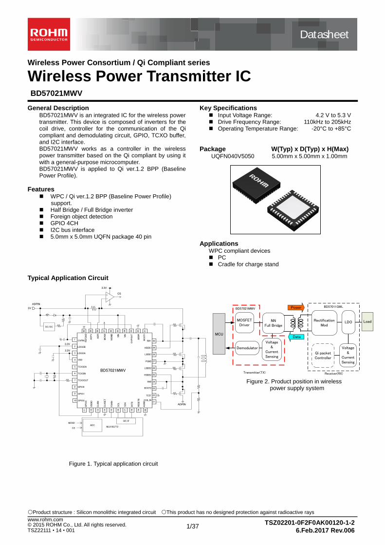
Wireless Power Consortium / Qi Compliant series
Wireless Power Transmitter IC BD57021MWV
General Description BD57021MWV is an integrated IC for the wireless power transmitter. This device is composed of inverters for the coil drive, controller for the communication of the Qi compliant and demodulating circuit, GPIO, TCXO buffer, and I2C interface. BD57021MWV works as a controller in the wireless power transmitter based on the Qi compliant by using it with a general-purpose microcomputer. BD57021MWV is applied to Qi ver.1.2 BPP (Baseline Power Profile).
Features WPC / Qi ver.1.2 BPP (Baseline Power Profile)
support. Half Bridge / Full Bridge inverter Foreign object detection GPIO 4CH I2C bus interface 5.0mm x 5.0mm UQFN package 40 pin
Key Specifications Input Voltage Range: 4.2 V to 5.3 V Drive Frequency Range: 110kHz to 205kHz Operating Temperature Range: -20°C to +85°C
Package W(Typ) x D(Typ) x H(Max) UQFN040V5050 5.00mm x 5.00mm x 1.00mm
Applications WPC compliant devices PC Cradle for charge stand
Typical Application Circuit
Figure 2. Product position in wireless power supply system
Figure 1. Typical application circuit
5V
ML610Q772ADC
I2C IF
CS
MONI1
ADPIN
40 39 38 37 36 35 34 33 32 31
1
2
3
4
5
6
7
8
9
10
11 12 13 14 15 16 17 18 19 20
30
29
28
27
26
25
24
23
22
21
TCXOOUT
LDO33A
LDO33B
GPIO0
GPIO1
GPIO2
TCXOIN
OVPIN
TCXOEN
VDD
CLKSET
AG
ND
INTB
GP
IO3
SD
A
CLKIN
SC
L
RESETB
FSKIN
VD
DIO
COIL_IN
TEST
LSIDE1
SW1
BOOT2
HSIDE2
LSIDE2
SW2
HSIDE1
PGND
MO
NI0
OV
PO
UT
REFG
ND
VIN
BO
OT1
AD
PV
MO
NI1
AD
PI
AD
DR
VIN
BD57021MWV
DC/DC
+
-
3.3V
CS
3.3V
3.3V
ADPIN
Datasheet

2/37
TSZ02201-0F2F0AK00120-1-2 © 2015 ROHM Co., Ltd. All rights reserved. 6.Feb.2017 Rev.006
www.rohm.com
TSZ22111 • 15 • 001
BD57021MWV
Absolute Maximum Ratings
Parameter Symbol Rating Unit
VIN, ADPV, ADPI, SW1, SW2 voltage VIN_H1 -0.3 to 7.0 V
BOOT1, BOOT2 voltage VIN_H2 -0.3 to 15.5 V
HSIDE1, HSIDE2 voltage VOUT_H -0.3 to 15.5 V
OVPIN, VDDIO, SCL, CLKIN, CLKSET, FSKIN, ADDR, TEST, RESETB voltage
VIN_L1 -0.3 to 7.0 V
VDD, TCXOIN voltage VIN_L2 -0.3 to 4.5 V
COIL_IN voltage VIN_L3 -4.5 to 7.0 V
LSIDE1, LSIDE2, LDO33A, LDO33B, OVPOUT, INTB, MONI0, MONI1 voltage
VOUT_L1 -0.3 to 7.0 V
TCXOEN, TCXOOUT voltage VOUT_L2 -0.3 to 4.5 V
SDA voltage VINOUT_L1 -0.3 to7.0 V
GPIO0, GPIO1, GPIO2, GPIO3 voltage VINOUT_L2 -0.3 to 4.5 V
Power dissipation Pd 3.26 (Note 1
) W
Operating ambient temperature range Ta -20 to +85 °C
Storage temperature range Tstg -55 to +150 °C
(Note 1) Derate by 26 mW/°C when operating above Ta=25°C (Mount on 4-layer 74.2mm x 74.2mm x 1.6mm board with front and back layer heat radiation
copper foil 4.5 mm x 4.5 mm, second and third layer heat radiation copper foil 74.2 mm x 74.2 mm). Caution: Operating the IC over the absolute maximum ratings may damage the IC. The damage can either be a short circuit between pins or an open circuit between pins and the internal circuitry. Therefore, it is important to consider circuit protection measures, such as adding a fuse, in case the IC is operated over the absolute maximum ratings.
Recommended Operating Conditions (Ta= -20°C to +85°C)
Parameter Symbol Min Typ Max Unit
VIN terminal input voltage range VIN 4.2 5.0 5.3 V
VDD terminal input voltage range VDD 3.1 3.3 3.5 V
VDDIO terminal voltage range VDDIO 3.1 3.3 3.5 V
Adapter input voltage range VADPV 4.2 5.0 5.3 V
TCXO terminal input frequency range FTCXO 32 - 45 MHz

3/37
TSZ02201-0F2F0AK00120-1-2 © 2015 ROHM Co., Ltd. All rights reserved. 6.Feb.2017 Rev.006
www.rohm.com
TSZ22111 • 15 • 001
BD57021MWV
Electrical Characteristics (Unless otherwise specified VIN=5V VDD=3.3V Ta=25°C)
Parameter Symbol Limit
Unit Conditions Min Typ Max
Whole Chip
Operating circuit current 1 ICC1 - 2.0 3.0 mA TCXOIN=0kHz
Operating circuit current 2 ICC2 - 15.0 23.0 mA TCXOIN=32MHz
Protection block (the IC outside)
External OCP operating voltage VOCP 125 160 195 mV RS=100mΩ
Protective circuit (the IC inside)
VIN Over voltage lockout VOVLO_VIN 6.1 6.4 6.7 V VIN: 5.0 → 8.0V
Hysteresis on OVLO VOVLO_HYS 140 200 260 mV VIN: 8.0 → 5.0V
VIN Under voltage lockout VUVLO_VIN 3.3 3.6 3.9 V VIN: 5.0 → 0V
Hysteresis on UVLO VUVLO_HYS 140 200 260 mV VIN: 0 → 5.0V
VDD UVLO detection voltage VUVLOD_VDD 2.25 2.50 2.75 V VDD: 3.3 → 0V
VDD UVLO release voltage VUVLOR_VDD 2.55 2.80 3.05 V VDD: 0 → 3.3V
VDDIO UVLO detection voltage VUVLOD_VDDIO 2.25 2.50 2.75 V VDDIO: 3.3 → 0V
VDDIO UVLO release voltage VUVLOD_VDDIO 2.55 2.80 3.05 V VDDIO: 0 → 3.3V
Internal OCP operating current IOCP - 0.48 0.65 A
LDO33A block
LDO33A output voltage VLDO33A 3.2 3.3 3.4 V Isource=10mA
LDO33A maximum output current ILDO33A - - 30 mA
LDO33B block
LDO33B output voltage VLDO33B 3.2 3.3 3.4 mV Isource=10mA
LDO33B maximum output current ILDO33B - - 30 mA
Demodulating circuit block
COIL_IN leak current 1 ILEAKCOILIN1 - - 50 µA VCOIL_IN=3.3V
COIL_IN leak current 2 ILEAKCOILIN2 -150 - - µA VCOIL_IN=-3.3V
TCXO_BUFF block
TCXOIN input current ITCXOIN - 0 1.0 µA VDD=VTCXOIN=4.5V
Input frequency range FTCXOIN - - 52 MHz
TCXOEN L level output voltage VOHTXCOEN - - VDD x 0.2
V Isink=1.0mA
TCXOEN H level output voltage VOLTXCOEN VDD x 0.8
- - V Isource=1.0mA
TCXOOUT output impedance ZOTCXOOUT - 1.0 - kΩ
Inverter block
Drive frequency FDRIVE 110 - 205 kHz
Minimum Duty Ratio Dutymin - 25 - %
Dead Time TDead - 200 - ns TCXOIN=32MHz
Source resistance RSOURCE - 1.0 - Ω
Sink resistance RSINK - 0.8 - Ω
GPIO block
GPIO L level input voltage VOLGPIO - - VDD x 0.3
V
GPIO H level input voltage VOHGPIO VDD x 0.7
- - V
GPIO pull-down resistor RPDGPIO - 100 kΩ
GPIO pull-up resister RPUGPIO - 100 - kΩ
GPIO L level output voltage VILGPIO - - VDD x 0.2
V Isink=1.0mA
GPIO H level output voltage VIHGPIO VDD x 0.8
- - V Isource=1.0mA
4/37
TSZ02201-0F2F0AK00120-1-2 © 2015 ROHM Co., Ltd. All rights reserved. 6.Feb.2017 Rev.006
www.rohm.com
TSZ22111 • 15 • 001
BD57021MWV
Parameter Symbol Limit
Unit Conditions Min Typ Max
FSKIN terminal
FSKIN L level input voltage VILFSKIN - - VDDIO x 0.3
V
FSKIN H level input voltage VIHFSKIN VDDIO x 0.7
- - V
CLKIN terminal
CLKIN L level input voltage VILCLKIN - - VDDIO x 0.3
V
CLKIN H level input voltage VIHCLKIN VDDIO x 0.7
- - V
ADDR terminal
ADDR L level input voltage VILADDR - - VDDIO x 0.3
V
ADDR H level input voltage VIHADDR VDDIO x 0.7
- - V
INTB terminal
Open Drain ability on INTB VLINTB - 380 500 mV Isink=5.0mA
INTB leak current ILEAKINTB - - 2.0 µA VINTB=7.0V
RESETB terminal
RESETB L level input voltage VILRSTB - - VDD
x 0.3 V
RESETB H level input voltage VIHRSTB VDD x 0.7
- - V
RESETB pull-up resister RPDRSTB - 100 - kΩ
I2C interface
SCL, SDA L level input voltage VILI2C - - 0.50 V
SCL, SDA H level input voltage VIHI2C 1.50 - - V
SCL, SDA L level input current IILI2C -1.0 - - µA
SCL, SDA H level input current IIHI2C - - 1.0 µA
SDA L level output voltage VOLI2C - - 400 mV Isink=3.0mA
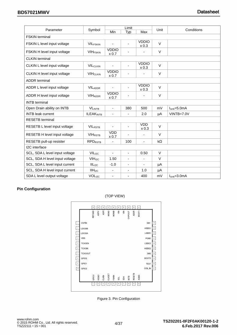
Pin Configuration
Figure 3. Pin Configuration
1
2
3
4
5
6
7
8
9
10
11 12 13 14 15 16 17 18 19 20
30
29
28
27
26
25
24
23
22
21
40 39 38 37 36 35 34 33 32 31
CLKSET
TCXOOUT
AG
ND
LDO33A
LDO33B
MO
NI0
INTB
GPIO0
GPIO1
GPIO2
GP
IO3
OV
PO
UT
COIL_IN
SD
A
REFG
ND
TEST
VIN
LSIDE1
BO
OT1
SW1
BOOT2
HSIDE2
LSIDE2
SW2
HSIDE1
AD
PV
CLKIN
SC
L
MO
NI1
RESETB
PGND
AD
PI
TCXOIN
FSKIN
AD
DR
OVPIN
TCXOEN
VDD
VD
DIO
VIN
(TOP VIEW)
5/37
TSZ02201-0F2F0AK00120-1-2 © 2015 ROHM Co., Ltd. All rights reserved. 6.Feb.2017 Rev.006
www.rohm.com
TSZ22111 • 15 • 001
BD57021MWV
Pin Description
Pin No. Pin Name Function I/O
1 OVPIN 5.0V input, connected to OVPOUT. I
2 LDO33B 3.3V LDO output. O
3 LDO33A 3.3V LDO output. O
4 VDD 3.3V supply. I
5 TCXOEN Connected to External oscillator. Control signal output. O
6 TCXOIN Connected to External oscillator. I
7 TCXOOUT Connected to External oscillator. O
8 GPIO0 General-purpose input and output terminal. I/O
9 GPIO1 General-purpose input and output terminal. I/O
10 GPIO2 General-purpose input and output terminal. I/O
11 GPIO3 General-purpose input and output terminal. I/O
12 VDDIO 3.3V supply. I
13 CLKIN Clock input terminal, leave this pin open. I
14 CLKSET Test terminal, leave this pin open. I
15 FSKIN FSK control signal input. I
16 SCL I2C clock input I
17 SDA I2C Data input and output. I/O
18 INTB Interrupt detection output. O
19 RESETB Control logic reset I/O
20 AGND Analog ground. I
21 COIL_IN Coil current / voltage input. I
22 TEST Test terminal, connected to GND. I
23 BOOT2 Connected to Boot strap capacitor. I
24 SW2 Connected to the source of high side FET and the drain of low side FET. I
25 HSIDE2 Connected to the gate of high side FET. O
26 LSIDE2 Connected to the gate of low side FET. O
27 PGND Power ground. I
28 LSIDE1 Connected to the gate of low side FET. O
29 HSIDE1 Connected to the gate of high side FET. O
30 SW1 Connected to the source of high side FET and the drain of low side FET. I
31 BOOT1 Connected to Boot strap capacitor. I
32 ADDR Slave Address change. I
33 OVPOUT 5.0V output, connected to OVPIN. O
34 VIN 5.0V Input power supply I
35 VIN 5.0V Input power supply I
36 MONI0 Coil current value output. O
37 MONI1 Input voltage value and input current value output. O
38 ADPI Sense transmitter Input current. I
39 ADPV Sense transmitter Input voltage. I
40 REFGND Reference ground. I

6/37
TSZ02201-0F2F0AK00120-1-2 © 2015 ROHM Co., Ltd. All rights reserved. 6.Feb.2017 Rev.006
www.rohm.com
TSZ22111 • 15 • 001
BD57021MWV
DRIVERLDO
LDOLDO33A
DEMOD
VDD
TCXO Buff
UVLO
TSD
OVP
OSC
DRIVER
LDO33B
TCXOEN
TCXOIN
VIN
AD
PV
HSIDE2
HSIDE1
LSIDE2
BOOT2
SW2
BOOT1
SW1
LSIDE1
COIL_IN
INTB
RESETB
AD
DR
SD
APGND
AG
ND
REFG
ND
AD
PI
FSKIN
TCXOOUT
CLKSET
SC
L
VD
DIO
VDD
POWER_SENSEOVPIN
OV
PO
UT
MO
NI1
VDD
VDD
CONTROLLogic
CLKIN
IO
VDD
GPIO
GPIO3
GPIO2
GPIO1
GPIO0MONI0
Block Diagram
Figure 4. Block diagram

7/37
TSZ02201-0F2F0AK00120-1-2 © 2015 ROHM Co., Ltd. All rights reserved. 6.Feb.2017 Rev.006
www.rohm.com
TSZ22111 • 15 • 001
BD57021MWV
Description of Blocks
1. Pre-driver block
Transmitter (Tx) includes inverter circuits to input AC electricity into both ends of the primary coil and to produce the electromotive force on the secondary side by electromagnetic induction. BD57021MWV includes two pre-driver blocks to support Half Bridge inverter and Full Bridge inverter configurations. For the Half Bridge inverter configuration, it is necessary to set the pre-driver 1 (PWM0 signal). For the Full Bridge inverter configuration, it is necessary to set the pre-driver 1 and pre-driver 2 (PWM1 signal). The output power control modes are the frequency control, the duty control and the phase control. The pre-driver block prevents a through current by monitoring the on/off timing of low side FET and high side FET. For high efficiency, the bootstrap drive system which sets the H side-L side to Nch FET is adopted. It is necessary to put a capacitor (0.1 – 0.47 µF) between the BOOT1 (BOOT2) terminal and the SW1 (SW2) terminal to maintain the voltage potential between these pins. Install a ceramic capacitor as close to these pins as possible.
2. Digital Ping
Tx inputs AC electricity into the primary coil and by electromagnetic induction develops an electromotive force on the secondary coil which starts the Receiver (Rx). This phase is called Digital Ping. Tx keeps transmitting power as long as it receives Digital Ping from the Rx. Tx controls the transmission power based on a packet including the power incoming information from Rx. The following registers are used to configure Digital Ping.
(1) PWM0PRD: Setting register for the period of PWM0 signal
This register is used to set the period of PWM0 signal. The PWM0 signal sets the period of the pulse to be output from pre-driver 1 with a count level. The relation between the period of PWM0 signal and source clock is determined by the following formula:
10
kTargetCloc
kSourceClocroundPRDPWM
Where “round” means rounding off to the nearest whole number, and the source clock is from the TCXO. For example, if source clock=32MHz and target clock=100kHz, PWM0PRD register is set to the following value:
0x013F3191100
320000
roundPRDPWM
Name Address b7 b6 b5 b4 b3 b2 b1 b0 Initial Value
R/W
PWM0 PRDL
0x20 PWM0 PRD7
PWM0 PRD6
PWM0 PRD5
PWM0 PRD4
PWM0 PRD3
PWM0 PRD2
PWM0 PRD1
PWM0 PRD0
0x00 R/W
PWM0 PRDH
0x21 PWM0 PRD15
PWM0 PRD14
PWM0 PRD13
PWM0 PRD12
PWM0 PRD11
PWM0 PRD10
PWM0 PRD9
PWM0 PRD8
0x00 R/W
After PWM0DTYH (0x23) is written, this register is updated with the new data.
(2) PWM0DTY: Setting register for the duty of PWM0 signal
This register is used to set the duty of PWM0 signal. PWM0 signal is the output signal at pre-driver 1. The duty of PWM0 signal is set with the count number of the source clock. After this register has been written, when the counter number of PWM0 signal becomes 0, the data of PWM0PRD register and PWM0DTY register are updated with the new data. The relation between the duty of PWM0 signal and source clock is determined by the following formula:
100100
DutyPRDPWMintDTYPWM
Where “int” means rounding down to the nearest whole number and the source clock is from TCXO. For example, if source clock= 32MHz and target clock=100kHz with duty=50%, PWM0DTY register is set to the following value:
0x00A0160100
5013200
intDTYPWM

8/37
TSZ02201-0F2F0AK00120-1-2 © 2015 ROHM Co., Ltd. All rights reserved. 6.Feb.2017 Rev.006
www.rohm.com
TSZ22111 • 15 • 001
BD57021MWV
Duty is defines as the ratio between the amount of time when the output is high in one period to the whole period of PWM0 signal. The enable range of PWM0DTY register is from 0x0001 to (PWM0PRD-1). PWM0 will not be generated if the PWM0DTY register is set to a value greater than or equal to the value in PWM0PRD register.
Name Address b7 b6 b5 b4 b3 b2 b1 b0 Initial Value
R/W
PWM0 DTYL
0x22 PWM0 DTY7
PWM0 DTY6
PWM0 DTY5
PWM0 DTY4
PWM0 DTY3
PWM0 DTY2
PWM0 DTY1
PWM0 DTY0
0x00 R/W
PWM0 DTYH
0x23 PWM0 DTY15
PWM0 DTY14
PWM0 DTY13
PWM0 DTY12
PWM0 DTY11
PWM0 DTY10
PWM0 DTY9
PWM0 DTY8
0x00 R/W
(3) PWM1PHS: Setting register for the phase difference between PWM1 signal and PWM0 signal
This register is used to set the phase difference between PWM1 signal and PWM0 signal with the count number of the source clock. PWM1 signal is a signal with the same period and duty as PWM0 signal. After PWM0DTYH register (0x23) is written and the counter number of PWM0PRD register becomes 0, the data of this register is updated with the new data. The enable range of this register is from 0x0001 to (PWM0PRD). PWM1 signal will not be generated if the PWM1PHS register is set to a value greater than or equal to the value in PWM0PRD register. It is also necessary to write 0x23 in PWM0DTYH register after this register has been written.
Name Address b7 b6 b5 b4 b3 b2 b1 b0 Initial Value
R/W
PWM1 PHSL
0x24 PWM1 PHS7
PWM1 PHS6
PWM1 PHS5
PWM1 PHS4
PWM1 PHS3
PWM1 PHS2
PWM1 PHS1
PWM1 PHS0
0x00 R/W
PWM1 PHSH
0x25 PWM1 PHS15
PWM1 PHS14
PWM1 PHS13
PWM1 PHS12
PWM1 PHS11
PWM1 PHS10
PWM1 PHS9
PWM1 PHS8
0x00 R/W
(4) PWM0GEN: Setting register for the dead time of PWM0 signal
This register is used to set the dead time of PWM0 signal. The relation between the dead time and the source clock is defined by the following formula:
kSourceCloc
DeadTime2
For example, if source clock=32MHz, Dead Time is the smallest value and it is 62.5nsec. Additionally, please set this register to the following value. Full Bridge inverter: PWMGEN0= 0x49 Half Bridge inverter: PWMGEN0= 0x10
Name Address b7 b6 b5 b4 b3 b2 b1 b0 Initial Value
R/W
PWMGEN0 0x30 P0DLY
D1 P0DLY
D0 P0DLY
C2 P0DLY
C1 P0DLY
C0 P0DLY
B2 P0DLY
B1 P0DLY
B0 0x92 R/W
(5) PWM1GEN: Setting register for the dead time of PWM1 signal
This register is used to set the dead time of PWM1 signal. The relation between the dead time and source clock is determined by the following formula:
kSourceCloc
DeadTime2
For example, if source clock=32MHz, Dead Time is the smallest value and it is 62.5nsec. Additionally, please set this register to the following value. Full Bridge inverter: PWMGEN1= 0x49 Half Bridge inverter: PWMGEN1= 0x10
Name Address b7 b6 b5 b4 b3 b2 b1 b0 Initial Value
R/W
PWMGEN1 0x31 P1DLY
D1 P1DLY
D0 P1DLY
C2 P1DLY
C1 P1DLY
C0 P1DLY
B2 P1DLY
B1 P1DLY
B0 0x92 R/W
(6) PWRCTRL: Setting register for the operation mode
This register is used to set the operation mode and the base clock for the internal movement. By setting the power mode bit (PWMD0, PWMD1), the operation mode is changed. The operation mode is Digital Ping when PWMD=0x0. Meanwhile, the operation mode is Analog Ping, which is also the low power consumption mode, when PWMD=0x1. On the other hand, the operation is Stop Mode when PWMD=0x3. During Stop Mode, all blocks are stopped. BD57021MWV uses the input clock signal from TCXOIN terminal for source clock of the internal movement. Please set this register with TCXSEL = 1, and connect TCXO with frequency between 32 to 52MHz to TCXOIN terminal. When TCXSEL = 1 and TCXEN = 1, TCXOEN terminal becomes high output but when TCXSEL = 1 and TCXEN = 0,

9/37
TSZ02201-0F2F0AK00120-1-2 © 2015 ROHM Co., Ltd. All rights reserved. 6.Feb.2017 Rev.006
www.rohm.com
TSZ22111 • 15 • 001
BD57021MWV
TCXOEN terminal becomes low output. Please set this register with OSCSEL= 1 to use an internal oscillator clock for measuring Analog Ping internal period.
・[7:6] Reserved
・[5:4] PWMD0, PWMD1: Setting bit for operation mode
(0x0: Digital Ping mode 0x1: Analog Ping mode 0x2: Reserved 0x3: Stop mode)
・[3] Reserved
・[2] OSCSEL: Control bit for using internal oscillator
(0x1: Enable 0x0: Disable)
・[1] TCXEN: Control bit for using external TCXO
(0x1: Enable (High output) 0x0: Disable (Low output))
・[0] TCXSEL: Selection bit for using external TCXO
(0x1: Enable 0x0: Disable)
Name Address b7 b6 b5 b4 b3 b2 b1 b0 Initial Value
R/W
PWRCTRL 0x0F -* 1 -
* 1 PWMD1 PWMD0 -* 1
OSCSEL TCXEN TCXSEL 0x07 R/W *1 prohibited
(7) PDCTRL: Control register for the pre-driver output
This register is used to enable pre-driver 1 and pre-driver 2. Pre-driver 1 drives HSIDE1 terminal and LSIDE1 terminal while pre-driver 2 drives HSIDE2 terminal and LSIDE2 terminal. When PDEN=1, the pulse is produced at HSIDE1 terminal and LSIDE1 terminal. When PDEN=0, the pulse is stopped. When PWM1EN=1, the pulse is produced at HSIDE2 terminal and LSIDE2 terminal. When PWM1EN=0, the pulse is stopped. Refer to 3. FSK (Frequency Shift Keying) for the explanation of PSWEN and PS256.
・[7:5] Reserved
・[4] PWM1EN: Control bit for pre-driver 2
(0x1: Enable 0x0: Disable)
・[3] Reserved
・[2] PS256: Change the PWM output to every 256 cycles
・[1] PSWEN: Control of the PWM change function
・[0] PDEN: Control bit for pre-driver 1
(0x1: Enable 0x0: Disable)
Name Address b7 b6 b5 b4 b3 b2 b1 b0 Initial Value
R/W
PDCTRL0 0x12 -* 1 -
* 1 -* 1
PWM1 EN
-* 1
PS256 PSWEN PDEN 0x00 R/W
*1 prohibited
3. FSK (Frequency Shift Keying)
BD57021MWV transmits a packet to Rx using Frequency Shift Keying (FSK) to establish communication with Rx. When Tx transmits a packet using FSK, Tx changes the frequency of the PWM0 signal by pre-driver 1 into the drive frequency (fd) and the modulation frequency (fmod) every 256 periods. That drive frequency is the frequency of the PWM0 signal which set in 2.(1).That FSK modulation frequency is the frequency of the PWM0 signal which set in 3. The setting of FSK sets the following registers. (1) PWMXPRD: Setting register for the period of the PWM0 signal at FSK
This register is used to set the period of PWM0 signal when PSWEN=1 (PDCTRL0: 0x12) and FSKIN terminal = high. The relation between the period of PWM0 signal and source clock is determined by the formula below, and it is expressed in the same formula as PWM0PRD.
1
kTargetCloc
kSourceClocroundPWMXPRD
Where “round” means rounding off to the nearest whole number.
Name Address b7 b6 b5 b4 b3 b2 b1 b0 Initial Value
R/W
PWMX PRDL
0x26 PWMX PRD7
PWMX PRD6
PWMX PRD5
PWMX PRD4
PWMX PRD3
PWMX PRD2
PWMX PRD1
PWMX PRD0
0x00 R/W
PWMX PRDH
0x27 PWMX PRD15
PWMX PRD14
PWMX PRD13
PWMX PRD12
PWMX PRD11
PWMX PRD10
PWMX PRD9
PWMX PRD8
0x00 R/W
(2) PWMXDTY: Setting register for the duty of the PWM0 signal at FSK
This register is used to set the duty of PWM0 signal when PSWEN=1 (PDCTRL0: 0x12) and FSKIN terminal = high. The
10/37
TSZ02201-0F2F0AK00120-1-2 © 2015 ROHM Co., Ltd. All rights reserved. 6.Feb.2017 Rev.006
www.rohm.com
TSZ22111 • 15 • 001
BD57021MWV
relation between the duty of PWM0 signal and source clock is determined by the formula below, and it is expressed in a same formula as PWM0DTY.
1001
DutyPWMXPRDintPWMXDTY
Where “int” means rounding down to the nearest whole number.
Name Address b7 b6 b5 b4 b3 b2 b1 b0 Initial Value
R/W
PWMX DTYL
0x28 PWMX DTY7
PWMX DTY6
PWMX DTY5
PWMX DTY4
PWMX DTY3
PWMX DTY2
PWMX DTY1
PWMX DTY0
0x00 R/W
PWMX DTYH
0x29 PWMX DTY15
PWMX DTY14
PWMX DTY13
PWMX DTY12
PWMX DTY11
PWMX DTY10
PWMX DTY9
PWMX DTY8
0x00 R/W
(3) PDCTRL: Control register for pre-driver output
This register is used to change the frequency of PWM0 signal by setting PSWEN and PS256. When PSWEN=1, the frequency and duty of PWM0 signal are changed by input signal of FSKIN terminal.
・When PSWEN = 0, the data of PWM0 signal is updated to the data of PWM0PRD and PWM0DTY.
・When of PSWEN = 1 and FSKIN terminal = Low, the data of PWM0 signal is updated to the data of PWM0PRD
register and PWM0DTY register.
・When of PSWEN = 1 and FSKIN terminal = High, the data of PWM0 signal is updated to the data of PWMXPRD
register and PWMXDTY register. When PS256 is 1, the period and the duty of PWM0 are changed by input signal of FSKIN terminal every 256 cycles. After having taken in a change of external terminal FSKIN, during 256 cycles of the output frequency, the next change isn’t taken. Furthermore, an interrupt occurs every 256 cycles of the output frequency when PXIEN bit of register INTENB (0x04) is 1. Whenever an interrupt occurs, the output frequency from a pre-driver is changed by changing input of external terminal FSKIN every 256 cycles. Refer to 2.Digital Ping (7) PDCTRL for the explanation of bits.
Name Address b7 b6 b5 b4 b3 b2 b1 b0 Initial Value
R/W
PDCTRL0 0x12 -* 1 -
* 1 -* 1
PWM1 EN
-* 1
PS256 PSWEN PDEN 0x00 R/W
*1 prohibited
4. Analog Ping
BD57021MWV outputs pulse signal from primary coil to detect if Rx was put on the interface of the Tx. The presence of Rx is confirmed if BD57021MWV detects a change in the coil current or voltage. When the change of the coil current or voltage reaches the threshold value of the Analog Ping detection, the state shifts to Digital Ping. Additionally, BD57021MWV will generate an interrupt after Analog Ping executes a set number of times. In Analog Ping, it is necessary to drive a primary coil near the resonant frequency. The setting of the frequency is performed right before an output of Analog Ping, like Digital Ping. Set the following registers to configure Analog Ping. (1) APGCTRL: Control register for Analog Ping
This register is used to set the start and stop of Analog Ping and the expected value of Rx detection by Analog Ping. BD57021MWV starts Analog Ping when APEN=1 is set. The period and duty of PWM0 should be set before APEN is set to 1. BD57021MWV stops Analog Ping when APEN=0 is set. When the state of the COIL_IN terminal is matched with the expected value of this register, BD57021MWV detects Rx. When APEN is 1, BD57021MWV becomes the stand-by state, the circuit electric current decreases.BD57021MWV will execute Analog ping until any of the two conditions is met: 1.) Analog Ping finishes the set number of repeated execution without detecting any Rx. 2.) Rx is detected wherein it generates an interrupt and stops Analog Ping. The expected value of Analog Ping is configured as follows:
・[7] APEN: Control bit for Analog Ping
(0x1: Enable 0x0:Disable)
・[6:2] Reserved
・[1:0] APEX0, APEX1: Expected value of Analog ping
(0x1: Detect the Rx 0x0: Not detect the Rx 0x2, 0x3: Reserved)
Name Address b7 b6 b5 b4 b3 b2 b1 b0 Initial Value
R/W
APGCTRL 0x16 APEN -* 1 -
* 1 -* 1 -
* 1 -* 1 APEX1 APEX0 0x00 R/W
*1 prohibited

11/37
TSZ02201-0F2F0AK00120-1-2 © 2015 ROHM Co., Ltd. All rights reserved. 6.Feb.2017 Rev.006
www.rohm.com
TSZ22111 • 15 • 001
BD57021MWV
(2) APGSTT: Analog Ping status register This register shows status of Analog Ping.
・[7] Reserved
・[6:4] APSTA2, APSTA1, APSTA0: Analog Ping status
0x0: Stop 0x1: Under the standby set in APGIVT 0x3: Under the power output set in APGIDUR 0x5: Under the measurement set in APGMSR 0x6: A state of the input accorded with a value of the APEX. BD57021MWV generates an interrupt and stop.
0x7: The number of Analog Ping cycles reaches the set number. BD57021MWV generates an interrupt and stop.
Others: Reserved ・[3:0] Reserved
Name Address b7 b6 b5 b4 b3 b2 b1 b0 Initial Value
R/W
APGSTT 0x17 -* 1
APSTA2 APSTA1 APSTA0 -* 1 -
* 1 -* 1 -
* 1 0x00 R/W *1 prohibited
(3) APGITVL: Setting register for the interval time of Analog Ping
This register is used to set the interval time of Analog Ping. If The Analog Ping detection interval is set short, time from Rx establishment on Tx to Tx starting power feeding is short. However, the power consumption of Tx increases The Analog Ping detection interval is set by interval with internal oscillation clock (typ.100kHz). The relation between the interval time and input clock is determined by the following formula:
1 InputClockmeIntervalTiAPGITV
For example, if Input Clock=100kHz and time of Interval Time=500msec, the value of APGITV register is set to the following value:
0xC34F499991100500 APGITV
Name Address b7 b6 b5 b4 b3 b2 b1 b0 Initial Value
R/W
APGITVL 0x18 APG ITV7
APG ITV6
APG ITV5
APG ITV4
APG ITV3
APG ITV2
APG ITV1
APG ITV0
0x00 R/W
APGITVH 0x19 APG ITV15
APG ITV14
APG ITV13
APG ITV12
APG ITV11
APG ITV10
APG ITV9
APG ITV8
0x00 R/W
(4) APGDUR: Setting register for the duration time of Analog Ping
This register is used to set the duration time of Analog Ping. Duration time is defined as the time frame wherein BD57021MWV produces the pulse output and drives the primary coil. The input clock from TCXOIN terminal is a source clock. The relation between the duration time and source clock is determined by the following formula:
11000
1
kSourceClocmeDurationTiintAPGDUR
Where “int” means rounding down to the nearest whole number. For example, if the time of duration is 100µsec and Source Clock is 32MHz, the value of APGDUR register is set to the following value:
0x0C7F319911000
132000100
intAPGDUR
Name Address b7 b6 b5 b4 b3 b2 b1 b0 Initial Value
R/W
APGDURL 0x1A APG
DUR7 APG
DUR6 APG
DUR5 APG
DUR4 APG
DUR3 APG
DUR2 APG
DUR1 APG
DUR0 0x00 R/W
APGDURH 0x1B -* 1 -
* 1 -* 1 -
* 1 APG
DUR11 APG
DUR9 APG
DUR8 APG
DUR7 0x00 R/W
*1 prohibited

12/37
TSZ02201-0F2F0AK00120-1-2 © 2015 ROHM Co., Ltd. All rights reserved. 6.Feb.2017 Rev.006
www.rohm.com
TSZ22111 • 15 • 001
BD57021MWV
(5) APGMSR: Setting register for the measurement time of Analog Ping This register is used to set the measurement time of Analog Ping. Measurement time is defined as the time frame after the duration time wherein BD57021MWV monitors the state of COIL_IN to confirm the presence of Rx. The input clock from TCXOIN terminal is a source clock. The relation between the measurement time and source clock is determined by the following formula:
11000
1
kSourceCloctTimeMeasuremenintAPGMSR
Where “int” means rounding down to the nearest whole number. For example, if Measurement Time=10µsec and Source Clock is 32MHz, APGMSR register is set to the following value:
0x013F31911000
13200010
intAPGMSR
Name Address b7 b6 b5 b4 b3 b2 b1 b0 Initial Value
R/W
APGMSRL 0x1C APG
MSR7 APG
MSR6 APG
MSR5 APG
MSR4 APG
MSR3 APG
MSR2 APG
MSR1 APG
MSR0 0x00 R/W
APGMSRH 0x1D -* 1
-* 1
-* 1
-* 1
APGMS
R11 APGMS
R10 APGMS
R9 APGMS
R8 0x00 R/W
*1 prohibited
(6) APGCNT: Setting register for the execution number of times of Analog Ping
This register is used to set the number of times Analog Ping carries out automatically. If APGCNT= 0, Analog Ping is carried out until APEN bit of APGCTRL register is 0. If APIEN=1 in the INTENB register, when the number of Analog Ping execution times reaches the set number, BD57021MWV generates an interrupt signal. BD57021MWV keeps generating an interrupt signal until APEN bit of APGCTRL register is 0.
Name Address b7 b6 b5 b4 b3 b2 b1 b0 Initial Value
R/W
APGCNT 0x1E APG CNT7
APG CNT6
APG CNT5
APG CNT4
APG CNT3
APG CNT2
APG CNT1
APG CNT0
0x00 R/W
5. Interrupt control
BD57021MWV generates various interrupt signals. These are configured by the following registers.
(1) INTSTT: Interrupt status register This register shows an interrupt status when an interrupt factor occurred. When any bit of this register is set, BD57021MWV generates an interrupt signal on INTB terminal. When the bit is set to 1, the interrupt signal is cleared.
・[7] Reserved
・[6] APINT: An interrupt signal of Analog Ping occurs.
・[5] Reserved
・[4] AGINT: An interrupt signal by the protection movement occurs.
・[3] EINT: An interrupt signal due to parity error or the framing error of the received packet.
・[2] CINT: An interrupt signal due to the check sum error occurs of the received packet.
・[1] RINT2: An interrupt signal due to the normal completion of reception by demodulator 2.
・[0] RINT1: An interrupt signal due to the normal completion of reception by demodulator circuit 1.
Name Address b7 b6 b5 b4 b3 b2 b1 b0 Initial Value
R/W
INTSTT 0x03 -* 1
APINT -* 1
AGINT EINT CINT RINT2 RINT1 0x00 R/W *1 prohibited
(2) INTENB: Control register for an interrupt
This register is used to control an interrupt signal. When the interrupt factor that is set to 1 by this register occurred, a bit to support of the interrupt status register is set. But there is no bit of the interrupt status register (INTSTT) corresponding to PXIEN of the interrupt enable register (INTENB). Because the admitted interrupt occurs in 1 pulse by PXIEN, the status at the time of the outbreak of interrupt is not maintained.
・[7] PXIEN: Control bit for an interrupt signal every 256 cycles by PWM change function
・[6] APINT: Control bit for an interrupt signal in Analog Ping
・[5] Reserved
・[4] AGINT: Control bit for an interrupt signal by protection movement
・[3] EINT: Control bit for an interrupt signal by the parity error or the framing error during the packet reception

13/37
TSZ02201-0F2F0AK00120-1-2 © 2015 ROHM Co., Ltd. All rights reserved. 6.Feb.2017 Rev.006
www.rohm.com
TSZ22111 • 15 • 001
BD57021MWV
・[2] CINT: Control bit for an interrupt signal by the check sum error during the packet reception
・[1] RINT2: Control bit for an interrupt signal by normal completion at demodulator 2 during the packet
reception
・[0] RINT1: Control bit for an interrupt signal by normal completion at demodulator 1 during the packet
reception
Name Address b7 b6 b5 b4 b3 b2 b1 b0 Initial Value
R/W
INTENB 0x04 PXIEN APIEN -* 1
AGIEN EIEN CIEN RIEN2 RIEN1 0x00 R/W *1 prohibited
6. AM demodulator block
BD57021MWV has the two AM demodulator blocks for communication with Rx. The characteristics of demodulator blocks are different to improve communication stability. The following registers are used for the configuration of the demodulator blocks.
(1) RXCTRL: Control register for Packet reception This register is used to control the demodulating blocks. If PRE1 bit=1, the demodulator 1 is enabled to receive the packets. If PRE2 bit=1, the demodulator 2 is enabled to receive the packets. It is possible to set both PRE1 bit and PRE2 bit to 1 at the same time, then demodulator 1 and demodulator 2 works independently. The digital filters of the demodulators are enabled if FTE1 bit and FTE2 bit are set to 1 in this register. In order to raise communication stability, please be sure that the digital filters are enabled. If other demodulator is receiving a packet even if reception error (frame error, parity error or check sum error) occurs in demodulator 1 or demodulator 2 while CTRL is 0, it does not generate an interrupt. If CTRL bit = 1 and a reception error occurs on demodulator 1 or demodulator 2, BD57021MWV generates an interrupt signal immediately.
・[7] CTRL: Setting bit of exclusive control function
(0x1: Enable 0x0: Disable)
・[6] Reserved
・[5] FTE2: Setting bit for the digital filter of the demodulator 2
(0x1: Enable 0x0: Disable)
・[4] FTE1: Setting bit for the digital filter of the demodulator 1
(0x1: Enable 0x0: Disable)
・[3:2] Reserved
・[1] PRE2: Setting bit for the demodulator 2
(0x1: Enable 0x0: Disable)
・[0] PRE1: Setting bit for the demodulator 1
(0x1: Enable 0x0: Disable)
Name Address b7 b6 b5 b4 b3 b2 b1 b0 Initial Value
R/W
RXCTRL 0x01 CTRL -* 1
FTE2 FTE1 -* 1
-* 1
PRE2 PRE1 0x00 R/W *1 prohibited
(2) RXSTT: Packet reception status register
This register holds the status of the packet reception of the demodulator. If packet reception with demodulator 1 is completed normally, RCV1 becomes 1. If packet reception with demodulator 2 is completed normally, RCV2 becomes 1. If check sum error occurs during the packet reception with demodulator 1 or demodulator 2, CERR becomes 1. If parity error or framing error occurs during the packet reception with demodulator 1 or demodulator 2, PERR becomes 1. The factors of the framing error during packet reception are as follows:
・Stop bit is not found.
・Reception was completed in the middle of a byte.
・The packet size that is calculated from the value of the header byte is different from the one that is received.
In addition, RCV1, RCV2, CERR and RERR, latch when packet reception is completed. These are cleared if RINT1, RINT2, CINT and RINT (INTSTT: 0x03) are written 1.These are overwritten when the next packet is received. When demodulator 1 is receiving packet, BSY1 becomes 1. When demodulator 2 is receiving packet, BSY2 becomes 1.
・[7] BSY2: Demodulator2 is busy receiving a packet
・[6] BSY1: Demodulator1 is busy receiving a packet
・[5:4] Reserved
・[3] PERR: Parity error or framing error occurred during the packet reception with either demodulator.
・[2] CERR: Check sum error occurred during the packet reception with either demodulator.
・[1] RCV2: Packet reception is completed normally with demodulator 2.
・[0] RCV1: Packet reception is completed normally with demodulator 1.
14/37
TSZ02201-0F2F0AK00120-1-2 © 2015 ROHM Co., Ltd. All rights reserved. 6.Feb.2017 Rev.006
www.rohm.com
TSZ22111 • 15 • 001
BD57021MWV
Name Address b7 b6 b5 b4 b3 b2 b1 b0 Initial Value
R/W
RXSTT 0x02 BSY2 BSY1 -* 1 -
* 1 RERR CERR RCV2 RCV1 0x00 R *1 prohibited
(3) CLKDIV: Register for setting Clock frequency division
This register sets the fundamental period of the demodulator. This set the fundamental period (CLKDIV) with a count level. The value of CLKDIV must be set so that Target Clock becomes 16kHz (62.5µsec). CLKDIV is determined by the following formula:
12
kTargetCloc
kSourceClocintCLKDIV
Where “int” means rounding down to the nearest whole number. For example, if Source Clock is 32MHz, CLKDIV set to the following value:
0x03E79991216
32000
intCLKDIV
Name Address b7 b6 b5 b4 b3 b2 b1 b0 Initial Value
R/W
CLKDIV1L 0x0C CLK DIV7
CLK DIV6
CLK DIV5
CLK DIV4
CLK DIV3
CLK DIV2
CLK DIV1
CLK DIV0
0xE7 R/W
CLKDIV1H 0x0D CLK
DIV15 CLK
DIV14 CLK
DIV13 CLK
DIV12 CLK
DIV11 CLK
DIV10 CLK DIV9
CLK DIV8
0x03 R/W
(4) FLTPRD: Register for setting filter fundamental period
This register appoints the fundamental period of the digital filter. This set the fundamental period (FLTPRD) with a count level. The value of CLKDIV must be set so that Target Clock becomes 2kHz (500µsec). FLTPRD is determined by the
following formula:
1
kTargetCloc
kSourceClocroundFLTPRD
Where “round” means rounding off to the nearest whole number. For example, when Source Clock is 32MHz, CLKDIV is set to the following value:
0x3E7F1599912
32000
roundFLTPRD
Name Address b7 b6 b5 b4 b3 b2 b1 b0 Initial Value
R/W
FLTPRDL 0xA0 FLT
PRD7 FLT
PRD6 FLT
PRD5 FLT
PRD4 FLT
PRD3 FLT
PRD2 FLT
PRD1 FLT
PRD0 0x00 R/W
FLTPRDH 0xA1 FLT
PRD15 FLT
PRD14 FLT
PRD13 FLT
PRD12 FLT
PRD11 FLT
PRD10 FLT
PRD9 FLT
PRD8 0x00 R/W
(5) RXSTT_1: Packet reception status register 1 This register shows the packet reception status of demodulator 1.
・[7] PRE1: In searching the preamble of the packet with demodulator 1
・[6] BSY1: In receiving a packet with demodulator 1
・[5] RDN1:Packet reception is completed with demodulator 1
・[4] ERF1:Framing error occurs during the packet reception with demodulator 1
・[3] ERP1:Parity error occurs during the packet reception with demodulator 1
・[2] ERC1:Check sum error occurs during the packet reception with demodulator 1
・[1] RCV2:Packet reception is completed with demodulator 2 normally
・[0] RCV1:Packet reception is completed with demodulator 1 normally
Name Address b7 b6 b5 b4 b3 b2 b1 b0 Initial Value
R/W
RXSTT_1 0x52 PRE1 BSY1 RDN1 ERF1 ERP1 ERC1 RCV2 RCV1 0x00 R

15/37
TSZ02201-0F2F0AK00120-1-2 © 2015 ROHM Co., Ltd. All rights reserved. 6.Feb.2017 Rev.006
www.rohm.com
TSZ22111 • 15 • 001
BD57021MWV
(6) RXSTT_2: Packet reception status register 2 This register shows the packet reception status of demodulator 2.
・[7] PRE2: In searching the preamble of the packet with demodulator 2
・[6] BSY2: In receiving a packet with demodulator 2
・[5] RDN2:Packet reception is completed with demodulator 2
・[4] ERF2:Framing error occurs during the packet reception with demodulator 2
・[3] ERP2:Parity error occurs during the packet reception with demodulator 2
・[2] ERC2:Check sum error occurs during the packet reception with demodulator 2
・[1] RCV1:Packet reception is completed with demodulator 1 normally
・[0] RCV2:Packet reception is completed with demodulator 2 normally
Name Address b7 b6 b5 b4 b3 b2 b1 b0 Initial Value
R/W
RXSTT_2 0x53 PRE2 BSY2 RDN2 ERF2 ERP2 ERC2 RCV1 RCV2 0x00 R
(7) RXCNT_X: Reports the Rx byte counter This register reports the total number of bytes received from demodulator 1 or 2.
・[7:5] Reserved
・[4] RXxCNT4 (x: 0, 1)
・[3] RXxCNT3 (x: 0, 1)
・[2] RXxCNT2 (x: 0, 1)
・[1] RXxCNT1 (x: 0, 1)
・[0] RXxCNT0 (x: 0, 1)
Name Address b7 b6 b5 b4 b3 b2 b1 b0 Initial Value
R/W
RXCNT_1 0x50 -*1
-*1
-*1
RX1
CNT4 RX1
CNT3 RX1
CNT2 RX1
CNT1 RX1
CNT0 0x00 R
RXCNT_2 0x51 -*1
-*1
-*1
RX2
CNT4 RX2
CNT3 RX2
CNT2 RX2
CNT1 RX2
CNT0 0x00 R
*1 prohibited
(8) RXDAT_1: Packet data register 1 This enables to show the data of the packet that is received with demodulator 1. Size of the buffers receiving Qi packet is 32 bytes. The longest packet prescribed in Qi is 29 bytes (including a header and the check sum byte). So BD57021MWV receive the packet of all kinds. The buffer to receive Qi packet is one to be 32 bytes, and the packet that is received is stored by the top of the buffer memory and is overwritten when BD57021MWV receive the next packet.
Name Address b7 b6 b5 b4 b3 b2 b1 b0 Initial Value
R/W
RXDAT_1 0x60
: 0x7F
Last 32 Bytes received by Demodulator 1 0x00 R
(9) RXDAT_2: Packet data register 2 This enables to show the data of the packet that is received with demodulator 2. Size of the buffers receiving Qi packet is 32 bytes. The buffer to receive Qi packet is one to be 32 bytes, and the packet that is received is stored by the top of the buffer memory and is overwritten when BD57021MWV receive the next packet.
Name Address b7 b6 b5 b4 b3 b2 b1 b0 Initial Value
R/W
RXDAT_2 0x80
: 0x9F
Last 32 Bytes received by Demodulator 2 0x00 R
7. About the input power detection
During wireless power transmission, when a foreign object such as a piece of metal exists on the charge interface between Tx and Rx, it generates heat, which poses a risk to cause burns and may even damage the Rx. BD57021MWV monitors the input power to the Tx and finds transmission electricity and detects the existence of the foreign object by comparing the transmission electricity with the received power electricity information (Received Power Packet) from Rx. BD57021MWV calculates the input power by monitoring the input voltage and the input current of the Tx.
About the input voltage detection, BD57021MWV can output the voltage of ADPV terminal voltage ×0.1 from MONI1
terminal by the following register setting. About the input current detection, BD57021MWV can output the voltage of
(ADPV terminal voltage - ADPI terminal voltage) ×10 from MONI1 terminal by the following register setting.
(1) AINSEL: Analog input choice register
By this register, MONI1 terminal outputs the voltage of ADPV terminal voltage ×0.1.

16/37
TSZ02201-0F2F0AK00120-1-2 © 2015 ROHM Co., Ltd. All rights reserved. 6.Feb.2017 Rev.006
www.rohm.com
TSZ22111 • 15 • 001
BD57021MWV
・[7:2] Reserved
・[1:0] AIN1SEL1, AIN1SEL0
(0x3:input current value 0x2:input voltage value)
Name Address b7 b6 b5 b4 b3 b2 b1 b0 Initial Value
R/W
AINSEL 0x08 -* 1 -
* 1 -* 1 -
* 1 -* 1 -
* 1 AIN1 SEL1
AIN1 SEL0
0x00 R/W
*1 prohibited
8. Low Drop OUT (LDO) block
BD57021MWV is equipped with two LDO blocks. On LDO33A terminal, it is assumed that the power supply of the microcomputer is connected. Capacitors (0.47 ~ 2.0uF) are necessary between the LDO terminals (LDO33A and LDO33B) and GND. Please place the capacitors as close to LDO33A and LDO33B terminals as possible.
9. About a general-purpose terminal (GPIO)
BD57021MWV has four GPIO terminals as a general-purpose terminal. The following registers are used to configure the GPIO terminals.
(1) GPDIR: Input and output direction setting register of the GPIO port This register sets each GPIO port as an input terminal or output terminal. If set to 1, the port becomes an output terminal. On the other hand, if set to 0, the port becomes an input terminal.
・[7:4] Reserved
・[3:0] PDX (X: 0- 3)
(0x1: Enable output on GPIOX 0x0:Enable input on GPIOX)
Name Address b7 b6 b5 b4 b3 b2 b1 b0 Initial Value
R/W
GPDIR 0x42 -* 1 -
* 1 -* 1 -
* 1 PD3 PD2 PD1 PD0 0x00 R/W *1 prohibited
(2) GPIN: Input state confirmation register of the GPIO terminal This register defines the state of the GPIO port. Only the bit set as an input port in the input and output direction setting registers of the GPIO port is enabled. When H is input into the port, the corresponded register becomes 1. When L was input into the port, the corresponded register becomes 0.
・[7:4] Reserved
・[3:0] PIX (X: 0- 3)
(0x1: High input on GPIOX 0x0:Low input on GPIOX)
Name Address b7 b6 b5 b4 b3 b2 b1 b0 Initial Value
R/W
GPIN 0x40 -* 1 -
* 1 -* 1 -
* 1 PI3 PI2 PI1 PI0 - R *1 prohibited
(3) GPOUT: Output setting register of the GPIO terminal This register sets an output level to the GPIO port. Only the bit set as an output port in the input and output direction setting registers of the GPIO port is enabled. When the register is 1, the corresponded port outputs H. When the register is 0, the corresponded port outputs L.
・[7:4] Reserved
・[3:0] POX (X: 0- 3)
(0x1: High output on GPIOX 0x0:Low output on GPIOX)
Name Address b7 b6 b5 b4 b3 b2 b1 b0 Initial Value
R/W
GPOUT 0x41 -* 1 -
* 1 -* 1 -
* 1 PO3 PO2 PO1 PO0 0x00 R/W *1 prohibited

17/37
TSZ02201-0F2F0AK00120-1-2 © 2015 ROHM Co., Ltd. All rights reserved. 6.Feb.2017 Rev.006
www.rohm.com
TSZ22111 • 15 • 001
BD57021MWV
(4) GPPU: The pull-up resistance of GPIO port setting register This register sets the pull-up resistance of each GPIO port. If set to 1, the resistance connected to VDD power supply is enabled. If set to 0, it is disabled.
・[7:4] Reserved
・[3:0] PPUX (X: 0- 3)
(0x1: Enable pull-up resistor on GPIOX 0x0:Disable)
Name Address b7 b6 b5 b4 b3 b2 b1 b0 Initial Value
R/W
GPPU 0x43 -* 1 -
* 1 -* 1 -
* 1 PPU3 PPU2 PPU1 PPU0 0x00 R/W *1 prohibited
(5) GPPD: The pull-down resistance of GPIO port setting register This register sets the pull-down resistance of each GPIO port. If set to 1, the resistance connected to GND is enabled. If set to 0, it is disabled. The initial value of this register is 0x0F, and the pull-down resistance is enabled.
・[7:4] Reserved
・[3:0] PPDX (X: 0- 3)
(0x1: Enable pull-down resistor on GPIOX 0x0:Disable)
Name Address b7 b6 b5 b4 b3 b2 b1 b0 Initial Value
R/W
GPPD 0x44 -* 1 -
* 1 -* 1 -
* 1 PPD3 PPD2 PPD1 PPD0 0x0F R/W *1 prohibited
10. Reporting the identify
BD57021MWV has a register to report its identify and version. These are read only.
Name Address b7 b6 b5 b4 b3 b2 b1 b0 Initial Value
R/W
IDENT 0x00 DID7 DID6 DID5 DID4 DID3 DID2 DID1 DID0 0x15 R

18/37
TSZ02201-0F2F0AK00120-1-2 © 2015 ROHM Co., Ltd. All rights reserved. 6.Feb.2017 Rev.006
www.rohm.com
TSZ22111 • 15 • 001
BD57021MWV
11. Protective circuit
BD57021MWV has the following functions as a protection feature.
Protection name
Detection terminal
Detection condition Release condition Protection type
OVLO_VIN VIN VIN > 6.4V VIN <6.2V System disabled
UVLO_VIN VIN VIN <3.4V VIN > 3.6V System disabled
Internal OCP VIN ICC > IOCP = 0.48A ICC <IOCP =
0.48A System disabled
External OCP ADPV ADPI
ADPV - ADPI > VOCP = 160mV
ADPV - ADPI <160mV
And Register (
Note 1)
0xB1 = 0x08 *
Pre-driver block stop The LSIDE = HSIDE = L output
UVLO_ADPV ADPV VIN <4.3V VIN > 4.5V Pre-driver block stop (
Note 2)
LSIDE = H, HSIDE = L
UVLO_VDD VDD VDD <2.5V VDD > 2.8V Power-on reset cancellation RESETB = L
UVLO_VDDIO VDDIO VDDIO <2.5V VDDIO > 2.8V IO block Disable
(Note1) It is necessary to reset it from a register to cancel external overcurrent protection. It can reset external overcurrent protection by writing in 0x08 at address 0xB1. However, please set 0 by all means because this register does not automatically return to 0 after setting it to 0x08.
(Note2) BD57021MWV can mask the pre-driver block stop even if it detects UVLO_ADPV depending on the register setting.
(1) ANA_STAT: Status register for internal blocks This register reports the status for internal blocks.
・[7:5] Reserved
・[4] TCX_READY
(0x1: Fault detected 0x0:No fault)
・[3] OCP
(0x1: Fault detected 0x0:No fault)
・[2] TSD
(0x1: Fault detected 0x0:No fault)
・[1] UVLO42
(0x1: Fault detected 0x0:No fault)
・[0] OVLO_VIN
(0x1: Fault detected 0x0:No fault)
Name Address b7 b6 b5 b4 b3 b2 b1 b0 Initial Value
R/W
ANA_STAT 0xB0 -*1 -
*1 -*1
TCX_READY
OCP TSD UVLO OVLO 0x00 R
*1 prohibited (2) ANA_ERR_CRL: OCP error configure register
This register configures the reset for OCP. If OCP_ERCL is set to 1, the OCP error is cleared. However, please set 0 by all means because this bit does not automatically return to 0 after setting it to 1.
Name Address b7 b6 b5 b4 b3 b2 b1 b0 Initial Value
R/W
ANN_ERR_ CRL
0xB1 -*1 -
*1 -*1 -
*1 OCP ERCL
-*1 -
*1 -
*1 0x00 R/W
*1 prohibited
(3) ERR_MODE: Error mode setting register in UVLO_ADPV This register configures the error mode in UVLO_ADPV. If ERR_SEL = 1, the pre-driver block works regardless of UVLO_ADPV. If ERR_SEL = 0, the pre-driver block stops if it detects UVLO_ADPV.
Name Address b7 b6 b5 b4 b3 b2 b1 b0 Initial Value
R/W
ERR_MODE 0xC4 -* 1 -
* 1 -* 1 -
* 1 -* 1 -
* 1 ERR_ SEL
-* 1
0x00 R/W
*prohibited
19/37
TSZ02201-0F2F0AK00120-1-2 © 2015 ROHM Co., Ltd. All rights reserved. 6.Feb.2017 Rev.006
www.rohm.com
TSZ22111 • 15 • 001
BD57021MWV
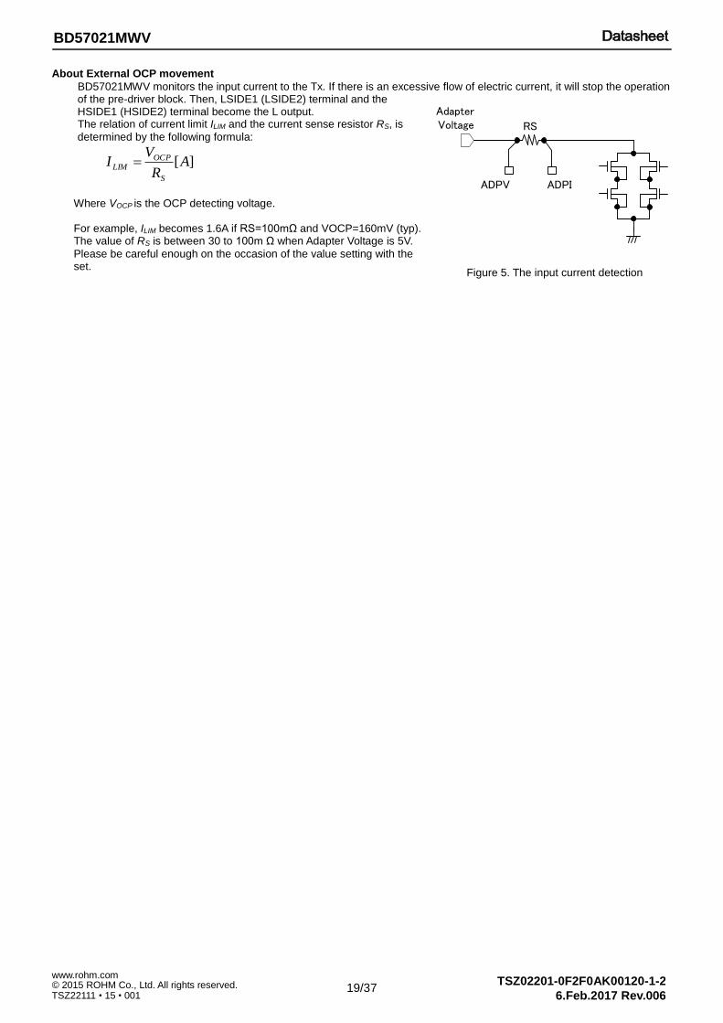
AdapterVoltage
ADPV ADPI
RS
About External OCP movement
BD57021MWV monitors the input current to the Tx. If there is an excessive flow of electric current, it will stop the operation of the pre-driver block. Then, LSIDE1 (LSIDE2) terminal and the HSIDE1 (HSIDE2) terminal become the L output. The relation of current limit ILIM and the current sense resistor RS, is
determined by the following formula:
][AR
VI
S
OCPLIM
Where VOCP is the OCP detecting voltage. For example, ILIM becomes 1.6A if RS=100mΩ and VOCP=160mV (typ). The value of RS is between 30 to 100m Ω when Adapter Voltage is 5V.
Please be careful enough on the occasion of the value setting with the set.
Figure 5. The input current detection

20/37
TSZ02201-0F2F0AK00120-1-2 © 2015 ROHM Co., Ltd. All rights reserved. 6.Feb.2017 Rev.006
www.rohm.com
TSZ22111 • 15 • 001
BD57021MWV
12. Command interface
12-1.Command Interface
I2C bus method is used in command interface with host CPU on BD57021MWV. In BD57021MWV, not only writing but read-out is possible except for some registers. Besides the slave address in BD57021MWV, one byte select address can be Specified, written and readout. The format of I2C bus slave mode is shown below. The slave address of BD57021MWV is 0x44 (7Bit) while ADDR terminal input is L. It is 0x45 (7Bit) while ADDR terminal input is H. MSB LSB MSB LSB MSB LSB
S Slave Address A Select Address A Data A P
S: Start condition Slave Address: Putting up the bit of read mode (H") or write mode (L") after slave address (7bit) set with ADDR, the data
of eight bits in total will be sent. (MSB first) A: The acknowledge bit in each byte adds into the data when acknowledge is sent and received. When data
is correctly sent and received, "L" will be sent and received. There was no acknowledging for "H". Select Address: 1 byte select address is used in BD57021MWV. (MSB first) Data: Data byte, data (the MSB first) sent and received P: Stop Condition
SDA
SCLS
Start Condition
Sr
Repeated Start Condition
Figure 6. Command Interface
Figure 7. Repeated Start Condition
SDA
SCL
MSB 6 5 LSB
Start Condition
When SDA↓, SCL=”H”
Stop Condition
When SDA↑, SCL=”H”

21/37
TSZ02201-0F2F0AK00120-1-2 © 2015 ROHM Co., Ltd. All rights reserved. 6.Feb.2017 Rev.006
www.rohm.com
TSZ22111 • 15 • 001
BD57021MWV
12-2.Data Format
Write format
b7 b6 b5 b4 b3 b2 b1 b0
R
/W
Slave Address
(7bit)
S
A
C
K
b7 b6 b5 b4 b3 b2 b1 b0
Select Address
(8bit)
A
C
K
b7 b6 b5 b4 b3 b2 b1 b0
Write Data
(8bit)
A
C
K
P
Start Condition '0' Write Acknowledge from
slave deviceStop Condition
Acknowledge from
slave device
Acknowledge from
slave device
Figure 8. Write Data Format
Read format
b7 b6 b5 b4 b3 b2 b1 b0
R
/W
Slave Address
(7bit)
S
A
C
K
b7 b6 b5 b4 b3 b2 b1 b0
Read Data
(8bit)
A
C
K
b7 b6 b5 b4 b3 b2 b1 b0
Read Data
(8bit)
N
A
K
P
Start Condition '1' Read Acknowledge from
slave deviceStop Condition
Acknowledge from
master device
Non acknowledge
from master device
Figure 9. Read Data Format
Read Data from specified Select Address
b7 b6 b5 b4 b3 b2 b1 b0
R
/W
Slave Address
(7bit)
S
A
C
K
b7 b6 b5 b4 b3 b2 b1 b0
Select Address
(8bit)
A
C
K
'0' Write
b7 b6 b5 b4 b3 b2 b1 b0
R
/W
Slave Address
(7bit)
Sr
A
C
K
b7 b6 b5 b4 b3 b2 b1 b0
Read Data
N
A
C
'1' Read
P
Read Data from Select Address
Repeated Start Condition
Figure 10. Read Data from specified Select Address (1)
b7 b6 b5 b4 b3 b2 b1 b0
R
/W
Slave Address
(7bit)
S
A
C
K
b7 b6 b5 b4 b3 b2 b1 b0
Select Address
(8bit)
A
C
K
'0' Read
b7 b6 b5 b4 b3 b2 b1 b0
R
/W
Slave Address
(7bit)
S
A
C
K
b7 b6 b5 b4 b3 b2 b1 b0
Read Data
N
A
C
'1' Read
PP
Read Data from Select Address
Figure 11. Read Data from specified Select Address (2)

22/37
TSZ02201-0F2F0AK00120-1-2 © 2015 ROHM Co., Ltd. All rights reserved. 6.Feb.2017 Rev.006
www.rohm.com
TSZ22111 • 15 • 001
BD57021MWV
12-3. Control signal specifications ○Bus line, I/O stage electrical specification and timing
Figure 12. Timing chart Table 12-1. SDAI and SCLI bus-line characteristic (Unless specified, Ta = 25 degrees Celsius, VDD=3.3V)
Parameter Sign Draft mode
Unit Min. Max.
1 SCL clock frequency fSCL 0 400 kHz
2 Bus free time between a "stop" condition and "start"
conditions tBUF 1.3 - μs
3
It is a "start" condition (retransmission) in hold time.
After this period,
The first clock pulse is generated.
tHDSTA 0.6 - μs
4 LOW state hold time of the SCL clock tLOW 1.3 - μs
5 HIGH state hold time of the SCL clock tHIGH 0.6 - μs
6 Setup time of the retransmission "start" condition tSUSTA 0.6 - μs
7 Data hold time tHDDAT 0 Note1)
- μs
8 Data setup time tSUDAT 100 - ns
9 Rise time of SDA and the SCL traffic light tR 20+0.1Cb 300 ns
10 Fall time for SDA and SCL signaling tF 20+0.1Cb 300 ns
11 Setup time of the "stop" condition tSUSTO 0.6 - μs
12 Capacitive load of each bus line Cb - 400 pF The above-mentioned numerical values are all the values corresponding to VIH min and VIL max level. Note1) To exceed an undefined area on falling edged of SCLI, transmission device should internally offer the hold-time of 300ns or more for SDAI signal
(VIH min of SCLI signal).
The above-mentioned characteristic is a theory value in IC design and it doesn't be guaranteed by shipment inspection. When problem occurs by any chance, we talk in good faith and correspond.
tB U F
tL O W
tR
tH D S T A
SP
tH D D A T
tF
tH IG H t
S U D A TtS U S T A
S r
tH D S T A
tS U S T O
P
S D A
S C L

23/37
TSZ02201-0F2F0AK00120-1-2 © 2015 ROHM Co., Ltd. All rights reserved. 6.Feb.2017 Rev.006
www.rohm.com
TSZ22111 • 15 • 001
BD57021MWV
12-4. List of registers
Name Address b7 b6 b5 b4 b3 b2 b1 b0 Initial Value
R/W
IDENT 0x00 DID7 DID6 DID5 DID4 DID3 DID2 DID1 DID0 0x15 R
RXCTRL 0x01 CTRL -* 1
FTE2 FTE1 -* 1
-* 1
PRE2 PRE1 0x00 R/W
RXSTT 0x02 BSY2 BSY1 -* 1
-* 1
RERR CERR RCV2 RCV1 0x00 R
INTSTT 0x03 -* 1
APINT -* 1
AGINT RINT CINT RINT2 RINT1 0x00 R/W
INTENB 0x04 PXIEN APIEN -* 1
AGIEN RIEN CIEN RIEN2 RIEN1 0x00 R/W
Reserved 0x05
: 0x07
-* 1
-* 1
-* 1
-* 1
-* 1
-* 1
-* 1
-* 1
- -* 1
AINSEL 0x08 -* 1
-* 1
-* 1
-* 1
-* 1
-* 1
AIN1 SEL1
AIN1 SEL0
0x00 R/W
Reserved 0x09
: 0x0B
-* 1
-* 1
-* 1
-* 1
-* 1
-* 1
-* 1
-* 1
- -* 1
CLKDIV1L 0x0C CLK DIV7
CLK DIV6
CLK DIV5
CLK DIV4
CLK DIV3
CLK DIV2
CLK DIV1
CLK DIV0
0xE7 R/W
CLKDIV1H 0x0D CLK
DIV15 CLK
DIV14 CLK
DIV13 CLK
DIV12 CLK
DIV11 CLK
DIV10 CLK DIV9
CLK DIV8
0x03 R/W
Reserved 0x0E -* 1
-* 1
-* 1
-* 1
-* 1
-* 1
-* 1
-* 1
- -* 1
PWRCTRL 0x0F -* 1
-* 1
PWMD1 PWMD0 -* 1
OSCSEL TCXEN TCXSEL 0x07 R/W
Reserved 0x10
: 0x11
-* 1
-* 1
-* 1
-* 1
-* 1
-* 1
-* 1
-* 1
- -* 1
PDCTRL0 0x12 -* 1
-* 1
-* 1
PWM1
EN -* 1
PS256 PSWEN PDEN 0x00 R/W
Reserved 0x13
: 0x15
-* 1
-* 1
-* 1
-* 1
-* 1
-* 1
-* 1
-* 1
- -* 1
APGCTRL 0x16 APEN -* 1
-* 1
-* 1
-* 1
-* 1
APEX1 APEX0 0x00 R/W
APGSTT 0x17 -* 1
APSTA2 APSTA1 APSTA0 -* 1
-* 1
-* 1
-* 1
0x00 R/W
APGITVL 0x18 APG ITV7
APG ITV6
APG ITV5
APG ITV4
APG ITV3
APG ITV2
APG ITV1
APG ITV0
0x00 R/W
APGITVH 0x19 APG ITV15
APG ITV14
APG ITV13
APG ITV12
APG ITV11
APG ITV10
APG ITV9
APG ITV8
0x00 R/W
APGDURL 0x1A APG
DUR7 APG
DUR6 APG
DUR5 APG
DUR4 APG
DUR3 APG
DUR2 APG
DUR1 APG
DUR0 0x00 R/W
APGDURH 0x1B -* 1
-* 1
-* 1
-* 1
APG
DUR11 APG
DUR9 APG
DUR8 APG
DUR7 0x00 R/W
APGMSRL 0x1C APG
MSR7 APG
MSR6 APG
MSR5 APG
MSR4 APG
MSR3 APG
MSR2 APG
MSR1 APG
MSR0 0x00 R/W
APGMSRH 0x1D APGMS
R15 APGMS
R14 APGMS
R13 APGMS
R12 APGMS
R11 APGMS
R10 APGMS
R9 APGMS
R8 0x00 R/W
APGCNT 0x1E APG CNT7
APG CNT6
APG CNT5
APG CNT4
APG CNT3
APG CNT2
APG CNT1
APG CNT0
0x00 R/W
Reserved 0x1F -* 1
-* 1
-* 1
-* 1
-* 1
-* 1
-* 1
-* 1
- -* 1
PWM0PRDL 0x20 PWM0 PRD7
PWM0 PRD6
PWM0 PRD5
PWM0 PRD4
PWM0 PRD3
PWM0 PRD2
PWM0 PRD1
PWM0 PRD0
0x00 R/W
PWM0PRDH 0x21 PWM0 PRD15
PWM0 PRD14
PWM0 PRD13
PWM0 PRD12
PWM0 PRD11
PWM0 PRD10
PWM0 PRD9
PWM0 PRD8
0x00 R/W
PWM0DTYL 0x22 PWM0 DTY7
PWM0 DTY6
PWM0 DTY5
PWM0 DTY4
PWM0 DTY3
PWM0 DTY2
PWM0 DTY1
PWM0 DTY0
0x00 R/W
PWM0DTYH 0x23 PWM0 DTY15
PWM0 DTY14
PWM0 DTY13
PWM0 DTY12
PWM0 DTY11
PWM0 DTY10
PWM0 DTY9
PWM0 DTY8
0x00 R/W
PWM1PHSL 0x24 PWM1 PHS7
PWM1 PHS6
PWM1 PHS5
PWM1 PHS4
PWM1 PHS3
PWM1 PHS2
PWM1 PHS1
PWM1 PHS0
0x00 R/W
PWM1PHSH 0x25 PWM1 PHS15
PWM1 PHS14
PWM1 PHS13
PWM1 PHS12
PWM1 PHS11
PWM1 PHS10
PWM1 PHS9
PWM1 PHS8
0x00 R/W
PWMXPRDL 0x26 PWMX PRD7
PWMX PRD6
PWMX PRD5
PWMX PRD4
PWMX PRD3
PWMX PRD2
PWMX PRD1
PWMX PRD0
0x00 R/W
PWMXPRDH 0x27 PWMX PRD15
PWMX PRD14
PWMX PRD13
PWMX PRD12
PWMX PRD11
PWMX PRD10
PWMX PRD9
PWMX PRD8
0x00 R/W
PWMXDTYL 0x28 PWMX DTY7
PWMX DTY6
PWMX DTY5
PWMX DTY4
PWMX DTY3
PWMX DTY2
PWMX DTY1
PWMX DTY0
0x00 R/W
PWMXDTYH 0x29 PWMX DTY15
PWMX DTY14
PWMX DTY13
PWMX DTY12
PWMX DTY11
PWMX DTY10
PWMX DTY9
PWMX DTY8
0x00 R/W
Reserved 0x2A
: 0x2F
-* 1
-* 1
-* 1
-* 1
-* 1
-* 1
-* 1
-* 1
- -* 1
PWMGEN0 0x30 P0DLY
D1 P0DLY
D0 P0DLY
C2 P0DLY
C1 P0DLY
C0 P0DLY
B2 P0DLY
B1 P0DLY
B0 0x92 R/W
*1 prohibited *0x in the head of for each character means a hex digit. If there is nothing, it means decimal numeral

24/37
TSZ02201-0F2F0AK00120-1-2 © 2015 ROHM Co., Ltd. All rights reserved. 6.Feb.2017 Rev.006
www.rohm.com
TSZ22111 • 15 • 001
BD57021MWV
Name Address b7 b6 b5 b4 b3 b2 b1 b0 Initial Value
R/W
PWMGEN1 0x31 P1DLY
D1 P1DLY
D0 P1DLY
C2 P1DLY
C1 P1DLY
C0 P1DLY
B2 P1DLY
B1 P1DLY
B0 0x92 R/W
Reserved 0x32
: 0x3F
-* 1
-* 1
-* 1
-* 1
-* 1
-* 1
-* 1
-* 1
- -* 1
GPIN 0x40 -* 1
-* 1
-* 1
-* 1
PI3 PI2 PI1 PI0 - R
GPOUT 0x41 -* 1
-* 1
-* 1
-* 1
PO3 PO2 PO1 PO0 0x00 R/W
GPDIR 0x42 -* 1
-* 1
-* 1
-* 1
PD3 PD2 PD1 PD0 0x00 R/W
GPPU 0x43 -* 1
-* 1
-* 1
-* 1
PPU3 PPU2 PPU1 PPU0 0x00 R/W
GPPD 0x44 -* 1
-* 1
-* 1
-* 1
PPD3 PPD2 PPD1 PPD0 0xFF R/W
Reserved 0x45
: 0x4F
-* 1
-* 1
-* 1
-* 1
-* 1
-* 1
-* 1
-* 1
- -* 1
RXCNT_1 0x50 -* 1
-* 1
-* 1
RX1 CNT4
RX1 CNT3
RX1 CNT2
RX1 CNT1
RX1 CNT0
0x00 R/W
RXCNT_2 0x51 -* 1
-* 1
-* 1
RX2 CNT4
RX2 CNT3
RX2 CNT2
RX2 CNT1
RX2 CNT0
0x00 R/W
RXSTT_1 0x52 PRE1 BSY1 RDN1 ERF1 ERP1 ERC1 RCV2 RCV1 0x00 R
RXSTT_2 0x53 PRE2 BSY2 RDN2 ERF2 ERP2 ERC2 RCV2 RCV1 0x00 R
Reserved 0x54
: 0x5F
-* 1
-* 1
-* 1
-* 1
-* 1
-* 1
-* 1
-* 1
- -* 1
RXDAT_1 0x60
: 0x7F
Last 32 Bytes received by Demodulator 1 0x00 R
RXDAT_2 0x80
: 0x9F
Last 32 Bytes received by Demodulator 2 0x00 R
FLTPRDL 0xA0 FLT
PRD7 FLT
PRD6 FLT
PRD5 FLT
PRD4 FLT
PRD3 FLT
PRD2 FLT
PRD1 FLT
PRD0 0x00 R/W
FLTPRDH 0xA1 FLT
PRD15 FLT
PRD14 FLT
PRD13 FLT
PRD12 FLT
PRD11 FLT
PRD10 FLT
PRD9 FLT
PRD8 0x00 R/W
Reserved 0xA2
: 0xAF
-* 1
-* 1
-* 1
-* 1
-* 1
-* 1
-* 1
-* 1
- -* 1
ANA_STAT 0xB0 -* 1
-* 1
-* 1
TCX_RE
ADY OCP TSD UVLO OVLO 0x02 R
ANA_ERR_ CLR
0xB1 -* 1
-* 1
-* 1
-* 1
OCP ERCL
-* 1
-* 1
-* 1
0x00 R/W
Reserved 0xB2
: 0xC3
-* 1
-* 1
-* 1 -
* 1 -
* 1 -
* 1 -
* 1 -
* 1 - -
* 1
ERR_MODE 0xC4 -* 1
-* 1
-* 1
-* 1
-* 1
-* 1
ERR_ SEL
-* 1
0x00 R/W
Reserved 0xC5
: 0xFF
-* 1
-* 1
-* 1
-* 1
-* 1
-* 1
-* 1
-* 1
- -* 1
*1 prohibited *0x in the head of for each character means a hex digit. If there is nothing, it means decimal numeral

25/37
TSZ02201-0F2F0AK00120-1-2 © 2015 ROHM Co., Ltd. All rights reserved. 6.Feb.2017 Rev.006
www.rohm.com
TSZ22111 • 15 • 001
BD57021MWV
Typical Performance Curves
Figure 13. ICC1 [mA] vs Temp. [°C]
(TCXOIN CLK = 0kHz)
Figure 14. ICC2 [mA] vs Temp. [°C]
(TCXOIN CLK = 32MHZ)
Figure 15. Output Voltage VLDO33A [V] vs Temp. [°C]
(Output Current = 0mA)
Figure 16. Output Voltage VLDO33A [V] vs Output current [mA]
(Temp. = 25°C)
3.00
3.10
3.20
3.30
3.40
3.50
3.60
0 10 20 30 40
Output Current [mA]
Ou
tpu
t V
olta
ge
VL
DO
33
A [V
]
3.00
3.10
3.20
3.30
3.40
3.50
3.60
-20 0 20 40 60 80
Temp. [℃]
Ou
tpu
t V
olta
ge
VL
DO
33
A [V
]
1.40
1.60
1.80
2.00
2.20
2.40
-20 0 20 40 60 80
Temp [℃]
Inp
ut C
urr
en
t Ic
c1
[m
A]
12.0
13.0
14.0
15.0
16.0
-20 0 20 40 60 80
Temp [℃]
Inp
ut C
urr
en
t Ic
c2
[m
A]

26/37
TSZ02201-0F2F0AK00120-1-2 © 2015 ROHM Co., Ltd. All rights reserved. 6.Feb.2017 Rev.006
www.rohm.com
TSZ22111 • 15 • 001
BD57021MWV
Typical Performance Curves - continued
Figure 17. System Efficiency [%] vs Rx Output Power [W]
(Rx=BD57011GWL,Vout=5V)
Timing Chart
Figure 18. Start up sequence
0
10
20
30
40
50
60
70
80
0.0 1.0 2.0 3.0 4.0 5.0
Rx Output Power [W]
Syste
m E
ffic
ien
cy [%
]
5V
VIN
LDO33B
TCXOEN
ADPV
5V
3.3V
LDO33A
3.3V
LSIDE1
・・・ ・・・
・・・・・・ ・・・
・・・
Analog Ping100 usec
Digital Ping70msecMin = 1msec
・・・
・・・ ・・・
・・・

27/37
TSZ02201-0F2F0AK00120-1-2 © 2015 ROHM Co., Ltd. All rights reserved. 6.Feb.2017 Rev.006
www.rohm.com
TSZ22111 • 15 • 001
BD57021MWV
Application Example 1) Recommended Circuit Diagram
CV33B
CV33A
3.3V
3.3VB
GND
RTCXOUT
TG_GPIO0
MO
NI1
-P
A1
1
2
3
4
5
6
7
8
9
10
OVPIN
LDO33B
LDO33A
VDD
TCXOEN
TCXOIN
TCXOOUT
GPIO0
GPIO1
GPIO2
GP
IO3
REFG
ND
AD
PV
AD
PI
MO
NI1
MO
NI0
VIN
VIN
OV
PO
UT
AD
D
BO
OT1
40
39
38
37
36
35
34
33
32
31
28
29
27
26
24
25
23
22
21
SW1
HSIDE1
LSIDE1
PGND
LSIDE2
HSIDE2
SW2
BOOT2
TEST
COIL_IN
GNDCBOOT1
LSIDE2
HSIDE2
CBOOT2
GND
VD
DIO
CLKIN
CLKSET
FSKIN
SC
L
SD
A
INTB
RESETB
AG
ND
11
12
13
14 15
16
17
18
19
20
GND
3.3V
RSCL
RSDA
RINTB
GND
CSCL
CSDA
U1BD57021MWV
RH1
RHD1
RL1
RLD1
PGND
LSIDE2
HSIDE2RH2
RHD2
RL2
RLD2
LTX1
MOS2
CS1
CS2
CS3
30
CS4
RS2
RS1
GNDPGND
JP4
JP3
COM-CH
12345
109876
JP2 PGND
D1
GNDCREG
CVCC3
GND
CPC
RPC1RPC2
RINV4 RINV3
LDC
CVCC1
PGND
LX
LX
VR
EG
VC
C
GN
D
PG
ND
PG
ND
STB
INV
SW
OU
T
1
2
3
4
5
6
7
8
TEST
PD1
PB0
NC4
PB1
PB2
PB3
PA2
TESTF
PD
2
PC
3
PD
3
PD
4
PC
2
PD
5
PA
1
9 10
11
12 13
14
15
16
24
23
22
20
21
19
18
17
PB7
PC7
VDD
VSS
NC20
PB6
PB5
PB4
RESET_N
PD
0
PC
0
PC
4
PC
5
PC
1
PC
6
PA
0
32
31
30
29
28
27
26
25
GND
R8
RCOILIN_GPO
GND
C4
MO
NI0
_PA
0
GNDCAIN0
RLED3 LED3
3.3V
3.3V
MONI1-PA1
CAIN1 GNDRLED2
LED2
RLED1
LED1
GND
C8
C2
U3BD8311NUV
RSIN+
RSIN-CSIN
OUTREF
IN-
IN+V+
GND
3.3V
PGND
PGND
CPA2
CSOUTPGND
RSOUTMONI0_PA0
VADPV
GNDADPV
PGNDGND
CADP2CADP1
LTX2
RVDL2
M3
PGND
RCOILIN_CPO
RVDH
RVDL
PGND
3.3V
CCLMP
RCLMP
U4INA199A1
1
2
3 4
5
6
CCOIL_IN
2,3,4,10
1
5,6,7
9
8
MOS12,3,4,10
1
9
8
5,6,7
GND
CVIN1
U2ML610Q772
COUT1 COUT2
ROSCOSC
COSC1 COSC2
GNDGND
RESET_N
TEST
VPP
RX-D
For Debugger
* Thermal Pad is connected to the GND.
Changing the software may cause the changing the circuit diagram.
Figure 19. Typical application circuit diagram
2) Part list
Parts Name Recommended Value Unit Recommended Part Maker Number
Tx Coil
LTX 6.3 µH 760 308 111 Würth 1
IC
U1 - BD57021MWV ROHM 1
U2 - ML610Q772 LAPIS 1
U3 - BD8311NUV ROHM 1
U4 - INA199A1 TI 1
OSC 32 MHz NX3225GA NDK 1
FET/Tr
MOS1, MOS2 11 A HS8K1 ROHM 2
M3 0.2 A RUE002N05 ROHM 1
Diode/LED
LED1, LED2 (Green) VF<2.0V - SML-P11MT ROHM 2
LED3 (Red) VF<2.0V - SML-P11VT ROHM 1
D1 0.5 A RB551VM-30 ROHM 1
Coil/Trans
COM-CH - ohm - - SHORT
LDC 2.2 µH - MURATA 1
Capacitor
CADP1 22 µF - MURATA 1
CADP2 0.1 µF - MURATA 1
CS1 0.1 µF GRM31C5C1H104JA01 MURATA 1
CS2 0.1 µF GRM31C5C1H104JA01 MURATA 1

28/37
TSZ02201-0F2F0AK00120-1-2 © 2015 ROHM Co., Ltd. All rights reserved. 6.Feb.2017 Rev.006
www.rohm.com
TSZ22111 • 15 • 001
BD57021MWV
Parts Name Recommended Value Unit Recommended Part Maker Number
CS3 0.1 µF GRM31C5C1H104JA01 MURATA 1
CS4 0.1 µF GRM31C5C1H104JA01 MURATA 1
CCOIL_IN 680 pF - MURATA 1
CCLMP - F - - -
CBOOT1, CBOOT2 0.22 µF - MURATA 2
CVCC1 10 µF - MURATA 1
CVCC3 1 µF - MURATA 1
CREG 1 µF - MURATA 1
CPC 10 pF - MURATA 1
COUT1 10 µF - MURATA 1
COUT2 - F - - -
CVIN1 0.1 µF - MURATA 1
CV33A 1 µF - MURATA 1
CV33B 1 µF - MURATA 1
COSC1 - F - - -
COSC2 - F - - -
CSCL 10 pF - MURATA 1
CSDA - F - MURATA -
CSIN 0.1 µF - MURATA 1
CSOUT 0.1 µF - MURATA 1
CPA2 0.01 µF - MURATA 1
C2 1 µF - MURATA 1
C4 4700 pF - MURATA 1
C8 2200 pF - MURATA 1
CAIN0 4700 pF - MURATA 1
CAIN1 2200 pF - MURATA 1
Resistor
RS1, RS2 75 mΩ - ROHM 2
RH1, RH2 20 Ω - ROHM 2
RHD1, RHD2 2 MΩ - ROHM 2
RL1, RL2 20 Ω - ROHM 2
RLD1, RLD2 - Ω - - -
RVDH 10 kΩ - ROHM 1
RVDL 6.2 kΩ - ROHM 1
RVDL2 3.6 kΩ - ROHM 1
RCLMP - Ω - - -
RINV3 120 kΩ - ROHM 1
RINV4 30 kΩ - ROHM 1
RPC1 100 kΩ - ROHM 1
RPC2 200 kΩ - ROHM 1
RSCL 1.5 kΩ - ROHM 1
RSDA 3.6 kΩ - ROHM 1
RINTB - Ω - - -
RTCXOUT 1 MΩ - ROHM 1
ROSC - Ω - - SHORT
RSIN- 1 Ω - ROHM 1
RSIN+ 1 Ω - ROHM 1
RSOUT 1 kΩ - ROHM 1
R8 36 kΩ - ROHM 1
RLED1, RLED2, RLDE3 3.6 kΩ - ROHM 3

29/37
TSZ02201-0F2F0AK00120-1-2 © 2015 ROHM Co., Ltd. All rights reserved. 6.Feb.2017 Rev.006
www.rohm.com
TSZ22111 • 15 • 001
BD57021MWV
3) Selection of Components Externally Connected
Component Symbol Limit Unit
BOOT1 (2) terminal strapping capacity
CBOOT1, CBOOT2 0.1 to 0.47 µF
LDO33A (B) terminal strapping capacity
CV33A, CV33B 0.47 to 2.0 µF
L Side FET gate resistance RL1, RL2 1.0 to 30 Ω
H Side FET gate resistance RH1, RH2 1.0 to 30 Ω
Input current sense resistance RS 30 to 100 mΩ
About the above operating condition, it is the value in the IC only. Please be careful enough on the occasion of the value setting with the set.
Power Dissipation
(UQFN040V5050 Package) Use a thermal design that allows for a sufficient margin by taking into account the permissible power dissipation (Pd) in actual operating conditions.
Figure 20. Power Dissipation Curve (Pd-Ta Curve)
0.0
0.5
1.0
1.5
2.0
2.5
3.0
3.5
0 25 50 75 100 125 150
AMBIENT TEMPERATURE : Ta [°C]
PO
WE
R D
ISS
IPA
TIO
N :
Pd [
W]
3.26W
* 74.2mm x 74.2mm x 1.6mm Glass Epoxy Board (front and back layer heat radiation copper foil 4.5 mm x 4.5 mm, second and third layer heat radiation copper foil 74.2 mm x 74.2 mm)

30/37
TSZ02201-0F2F0AK00120-1-2 © 2015 ROHM Co., Ltd. All rights reserved. 6.Feb.2017 Rev.006
www.rohm.com
TSZ22111 • 15 • 001
BD57021MWV
I/O equivalent circuits
VIN, OVPOUT terminal
OVPOUT
VIN
BOOT1, HSIDE1, SW1, LSIDE1, PGND terminal (BOOT2, HSIDE2, SW2, LSIDE2)
OVPOUT
BOOT1 (2)
HSIDE1 (2)
SW1 (2)
LSIDE1 (2)
PGND
OVPIN, LDO33A (LDO33B) terminal
LDO33A(B)
OVPIN
VDD,TCXOIN, TCXOOUT terminal
VDD
TCXOIN
TCXOOUT
VDD
VDD
VDD
TCXOEN terminal
VDD
TCXOEN
VDDIO, FSKIN (CLKSET, CLKIN, ADDR, TEST) terminal
CLKINCLKSET
FSKINADDRTEST
VDDIO
VDDIO

31/37
TSZ02201-0F2F0AK00120-1-2 © 2015 ROHM Co., Ltd. All rights reserved. 6.Feb.2017 Rev.006
www.rohm.com
TSZ22111 • 15 • 001
BD57021MWV
GPIO0 (GPIO1, 2, 3) terminal
GPIO0GPIO1GPIO2GPIO3
VDD
VDD
VDD
VDD
SCL terminal
VDDIO
SCL
SDA terminal
VDDIO
SDA
INTB terminal
INTB
MONI0 terminal
VDD
MONI0
RESETB terminal
RESETB
VDDVDD
COIL_IN terminal
COIL_IN
ADPV, ADPI terminal
ADPI
ADPV
MONI1 terminal
MONI1

32/37
TSZ02201-0F2F0AK00120-1-2 © 2015 ROHM Co., Ltd. All rights reserved. 6.Feb.2017 Rev.006
www.rohm.com
TSZ22111 • 15 • 001
BD57021MWV
Operational Notes
1. Reverse Connection of Power Supply
Connecting the power supply in reverse polarity can damage the IC. Take precautions against reverse polarity when connecting the power supply, such as mounting an external diode between the power supply and the IC’s power supply pins.
2. Power Supply Lines
Design the PCB layout pattern to provide low impedance supply lines. Separate the ground and supply lines of the digital and analog blocks to prevent noise in the ground and supply lines of the digital block from affecting the analog block. Furthermore, connect a capacitor to ground at all power supply pins. Consider the effect of temperature and aging on the capacitance value when using electrolytic capacitors.
3. Ground Voltage
Ensure that no pins are at a voltage below that of the ground pin at any time, even during transient condition.
4. Ground Wiring Pattern
When using both small-signal and large-current ground traces, the two ground traces should be routed separately but connected to a single ground at the reference point of the application board to avoid fluctuations in the small-signal ground caused by large currents. Also ensure that the ground traces of external components do not cause variations on the ground voltage. The ground lines must be as short and thick as possible to reduce line impedance.
5. Thermal Consideration
Should by any chance the power dissipation rating be exceeded the rise in temperature of the chip may result in deterioration of the properties of the chip. In case of exceeding this absolute maximum rating, increase the board size and copper area to prevent exceeding the Pd rating.
6. Recommended Operating Conditions
These conditions represent a range within which the expected characteristics of the IC can be approximately obtained. The electrical characteristics are guaranteed under the conditions of each parameter.
7. Inrush Current
When power is first supplied to the IC, it is possible that the internal logic may be unstable and inrush current may flow instantaneously due to the internal powering sequence and delays, especially if the IC has more than one power supply. Therefore, give special consideration to power coupling capacitance, power wiring, width of ground wiring, and routing of connections.
8. Operation Under Strong Electromagnetic Field
Operating the IC in the presence of a strong electromagnetic field may cause the IC to malfunction.
9. Testing on Application Boards
When testing the IC on an application board, connecting a capacitor directly to a low-impedance output pin may subject the IC to stress. Always discharge capacitors completely after each process or step. The IC’s power supply should always be turned off completely before connecting or removing it from the test setup during the inspection process. To prevent damage from static discharge, ground the IC during assembly and use similar precautions during transport and storage.
10. Inter-pin Short and Mounting Errors
Ensure that the direction and position are correct when mounting the IC on the PCB. Incorrect mounting may result in damaging the IC. Avoid nearby pins being shorted to each other especially to ground, power supply and output pin. Inter-pin shorts could be due to many reasons such as metal particles, water droplets (in very humid environment) and unintentional solder bridge deposited in between pins during assembly to name a few.
11. Unused Input Pins
Input pins of an IC are often connected to the gate of a MOS transistor. The gate has extremely high impedance and extremely low capacitance. If left unconnected, the electric field from the outside can easily charge it. The small charge acquired in this way is enough to produce a significant effect on the conduction through the transistor and cause unexpected operation of the IC. So unless otherwise specified, unused input pins should be connected to the power supply or ground line.

33/37
TSZ02201-0F2F0AK00120-1-2 © 2015 ROHM Co., Ltd. All rights reserved. 6.Feb.2017 Rev.006
www.rohm.com
TSZ22111 • 15 • 001
BD57021MWV
Operational Notes – continued
12. Regarding the Input Pin of the IC
This monolithic IC contains P+ isolation and P substrate layers between adjacent elements in order to keep them isolated. P-N junctions are formed at the intersection of the P layers with the N layers of other elements, creating a parasitic diode or transistor. For example (refer to figure below):
When GND > Pin A and GND > Pin B, the P-N junction operates as a parasitic diode. When GND > Pin B, the P-N junction operates as a parasitic transistor.
Parasitic diodes inevitably occur in the structure of the IC. The operation of parasitic diodes can result in mutual interference among circuits, operational faults, or physical damage. Therefore, conditions that cause these diodes to operate, such as applying a voltage lower than the GND voltage to an input pin (and thus to the P substrate) should be avoided.
Figure 21. Example of monolithic IC structure
13. Ceramic Capacitor
When using a ceramic capacitor, determine the dielectric constant considering the change of capacitance with temperature and the decrease in nominal capacitance due to DC bias and others.
14. Area of Safe Operation (ASO)
Operate the IC such that the output voltage, output current, and power dissipation are all within the Area of Safe Operation (ASO).
15. Thermal Shutdown Circuit(TSD)
This IC has a built-in thermal shutdown circuit that prevents heat damage to the IC. Normal operation should always be within the IC’s power dissipation rating. If however the rating is exceeded for a continued period, the junction temperature (Tj) will rise which will activate the TSD circuit that will turn OFF all output pins. When the Tj falls below the TSD threshold, the circuits are automatically restored to normal operation. Note that the TSD circuit operates in a situation that exceeds the absolute maximum ratings and therefore, under no circumstances, should the TSD circuit be used in a set design or for any purpose other than protecting the IC from heat damage.
16. Over Current Protection Circuit (OCP)
This IC incorporates an integrated overcurrent protection circuit that is activated when the load is shorted. This protection circuit is effective in preventing damage due to sudden and unexpected incidents. However, the IC should not be used in applications characterized by continuous operation or transitioning of the protection circuit.
N NP
+ P
N NP
+
P Substrate
GND
NP
+
N NP
+N P
P Substrate
GND GND
Parasitic
Elements
Pin A
Pin A
Pin B Pin B
B C
E
Parasitic
Elements
GNDParasitic
Elements
CB
E
Transistor (NPN)Resistor
N Region
close-by
Parasitic
Elements
34/37
TSZ02201-0F2F0AK00120-1-2 © 2015 ROHM Co., Ltd. All rights reserved. 6.Feb.2017 Rev.006
www.rohm.com
TSZ22111 • 15 • 001
BD57021MWV
Ordering Information
B D 5 7 0 2 1 M W V - E 2
Part Number
Package MWV: UQFN040V5050
Packaging and forming specification E2: Embossed tape and reel
Marking Diagrams
UQFN040V5050 (TOP VIEW)
D 5 7 0 2 1
Part Number Marking
LOT Number
1PIN MARK

35/37
TSZ02201-0F2F0AK00120-1-2 © 2015 ROHM Co., Ltd. All rights reserved. 6.Feb.2017 Rev.006
www.rohm.com
TSZ22111 • 15 • 001
BD57021MWV
Physical Dimension, Tape and Reel Information
Package Name UQFN040V5050

36/37
TSZ02201-0F2F0AK00120-1-2 © 2015 ROHM Co., Ltd. All rights reserved. 6.Feb.2017 Rev.006
www.rohm.com
TSZ22111 • 15 • 001
BD57021MWV
Revision History
Date Revision Changes
10.Aug.2015 003 New Release
10.Dec.2015 004
P13 Paragraph number correction 6. deletion P24 to P34 Header correction
P27 Input current sense resistance 33 to 100 → 30 to 100
11.Apr.2016 005
P1 Figure 1. Modified the figure.
P3 Electrical Characteristics Corrected the font of unit. P7 1. Pre-driver block Changed the sentence. Corrected the font of unit.
P11 (4) APGDUR Corrected the font of unit. P12 (5) APGMSR Corrected the font of unit. P13 (1) RXCTRL Changed the sentence. P14 (3) CLKDIV Corrected the font of unit.
P14 (4) FLTPRD Corrected the font of unit.
P17 About External OCP movement Changed the sentence.
P25 1) Recommended Circuit Diagram Modified the circuit diagram. P25 to P27 2) Parts list Modified the parts list.
6. Feb. 2017 006
P1 General Description / Features / Package Change the sentence. P7 (1) PWM0PRD, (2) PWM0DTY Change the sentence.
P9 (6) PWRCTRL Added the explanation.
P9 3. FSK Modified the sentence
P9 (1) PWMXPRD Change the sentence. P10 (2) PWMXDTY Change the sentence. P10 (3) PDCTRL Added the explanation. P11 (2) APGSTT Modified the sentence.
P11 (4) APGDUR Change the sentence.
P12 (5) APGMSR Change the sentence.
P12 5. Interrupt control Modified the sentence P12 (1) INTSTT Change the sentence. P13 (2) INTENB Change the sentence. Added the explanation. P13 (1) RXCTRL Change the sentence. P13 (2) RXSTT Change the sentence. P14 (3) CLKDIV, (4) FLTPRD, (5) RXSTT_1 Change the sentence.
P15 (6) RXSTT_2 Change the sentence.
P15 (7) RXCNT_X Added the explanation.

37/37
TSZ02201-0F2F0AK00120-1-2 © 2015 ROHM Co., Ltd. All rights reserved. 6.Feb.2017 Rev.006
www.rohm.com
TSZ22111 • 15 • 001
BD57021MWV
Date Revision Changes
6. Feb. 2017 006
P15 (8) RXDAT_1, (9) RXDAT_2 Change the sentence.
P16, 17 (1) – (5) Added the explanation.
P17 10. Reporting the Identify Added the explanation
P18 (1) ANA_STAT, (2) ANA_ERR_CRL Added the explanation.
P19 About External OCP movement Change the sentence
P24 List of registers Modified

Notice-PGA-E Rev.003
© 2015 ROHM Co., Ltd. All rights reserved.
Notice
Precaution on using ROHM Products 1. Our Products are designed and manufactured for application in ordinary electronic equipments (such as AV equipment,
OA equipment, telecommunication equipment, home electronic appliances, amusement equipment, etc.). If you intend to use our Products in devices requiring extremely high reliability (such as medical equipment
(Note 1), transport
equipment, traffic equipment, aircraft/spacecraft, nuclear power controllers, fuel controllers, car equipment including car accessories, safety devices, etc.) and whose malfunction or failure may cause loss of human life, bodily injury or serious damage to property (“Specific Applications”), please consult with the ROHM sales representative in advance. Unless otherwise agreed in writing by ROHM in advance, ROHM shall not be in any way responsible or liable for any damages, expenses or losses incurred by you or third parties arising from the use of any ROHM’s Products for Specific Applications.
(Note1) Medical Equipment Classification of the Specific Applications
JAPAN USA EU CHINA
CLASSⅢ CLASSⅢ
CLASSⅡb CLASSⅢ
CLASSⅣ CLASSⅢ
2. ROHM designs and manufactures its Products subject to strict quality control system. However, semiconductor
products can fail or malfunction at a certain rate. Please be sure to implement, at your own responsibilities, adequate safety measures including but not limited to fail-safe design against the physical injury, damage to any property, which a failure or malfunction of our Products may cause. The following are examples of safety measures:
[a] Installation of protection circuits or other protective devices to improve system safety [b] Installation of redundant circuits to reduce the impact of single or multiple circuit failure
3. Our Products are designed and manufactured for use under standard conditions and not under any special or extraordinary environments or conditions, as exemplified below. Accordingly, ROHM shall not be in any way responsible or liable for any damages, expenses or losses arising from the use of any ROHM’s Products under any special or extraordinary environments or conditions. If you intend to use our Products under any special or extraordinary environments or conditions (as exemplified below), your independent verification and confirmation of product performance, reliability, etc, prior to use, must be necessary:
[a] Use of our Products in any types of liquid, including water, oils, chemicals, and organic solvents [b] Use of our Products outdoors or in places where the Products are exposed to direct sunlight or dust [c] Use of our Products in places where the Products are exposed to sea wind or corrosive gases, including Cl2,
H2S, NH3, SO2, and NO2
[d] Use of our Products in places where the Products are exposed to static electricity or electromagnetic waves [e] Use of our Products in proximity to heat-producing components, plastic cords, or other flammable items [f] Sealing or coating our Products with resin or other coating materials [g] Use of our Products without cleaning residue of flux (even if you use no-clean type fluxes, cleaning residue of
flux is recommended); or Washing our Products by using water or water-soluble cleaning agents for cleaning residue after soldering
[h] Use of the Products in places subject to dew condensation
4. The Products are not subject to radiation-proof design. 5. Please verify and confirm characteristics of the final or mounted products in using the Products. 6. In particular, if a transient load (a large amount of load applied in a short period of time, such as pulse. is applied,
confirmation of performance characteristics after on-board mounting is strongly recommended. Avoid applying power exceeding normal rated power; exceeding the power rating under steady-state loading condition may negatively affect product performance and reliability.
7. De-rate Power Dissipation depending on ambient temperature. When used in sealed area, confirm that it is the use in
the range that does not exceed the maximum junction temperature. 8. Confirm that operation temperature is within the specified range described in the product specification. 9. ROHM shall not be in any way responsible or liable for failure induced under deviant condition from what is defined in
this document.
Precaution for Mounting / Circuit board design 1. When a highly active halogenous (chlorine, bromine, etc.) flux is used, the residue of flux may negatively affect product
performance and reliability.
2. In principle, the reflow soldering method must be used on a surface-mount products, the flow soldering method must be used on a through hole mount products. If the flow soldering method is preferred on a surface-mount products, please consult with the ROHM representative in advance.
For details, please refer to ROHM Mounting specification

Notice-PGA-E Rev.003
© 2015 ROHM Co., Ltd. All rights reserved.
Precautions Regarding Application Examples and External Circuits 1. If change is made to the constant of an external circuit, please allow a sufficient margin considering variations of the
characteristics of the Products and external components, including transient characteristics, as well as static characteristics.
2. You agree that application notes, reference designs, and associated data and information contained in this document
are presented only as guidance for Products use. Therefore, in case you use such information, you are solely responsible for it and you must exercise your own independent verification and judgment in the use of such information contained in this document. ROHM shall not be in any way responsible or liable for any damages, expenses or losses incurred by you or third parties arising from the use of such information.
Precaution for Electrostatic This Product is electrostatic sensitive product, which may be damaged due to electrostatic discharge. Please take proper caution in your manufacturing process and storage so that voltage exceeding the Products maximum rating will not be applied to Products. Please take special care under dry condition (e.g. Grounding of human body / equipment / solder iron, isolation from charged objects, setting of Ionizer, friction prevention and temperature / humidity control).
Precaution for Storage / Transportation 1. Product performance and soldered connections may deteriorate if the Products are stored in the places where:
[a] the Products are exposed to sea winds or corrosive gases, including Cl2, H2S, NH3, SO2, and NO2 [b] the temperature or humidity exceeds those recommended by ROHM [c] the Products are exposed to direct sunshine or condensation [d] the Products are exposed to high Electrostatic
2. Even under ROHM recommended storage condition, solderability of products out of recommended storage time period may be degraded. It is strongly recommended to confirm solderability before using Products of which storage time is exceeding the recommended storage time period.
3. Store / transport cartons in the correct direction, which is indicated on a carton with a symbol. Otherwise bent leads
may occur due to excessive stress applied when dropping of a carton. 4. Use Products within the specified time after opening a humidity barrier bag. Baking is required before using Products of
which storage time is exceeding the recommended storage time period.
Precaution for Product Label A two-dimensional barcode printed on ROHM Products label is for ROHM’s internal use only.
Precaution for Disposition When disposing Products please dispose them properly using an authorized industry waste company.
Precaution for Foreign Exchange and Foreign Trade act Since concerned goods might be fallen under listed items of export control prescribed by Foreign exchange and Foreign trade act, please consult with ROHM in case of export.
Precaution Regarding Intellectual Property Rights 1. All information and data including but not limited to application example contained in this document is for reference
only. ROHM does not warrant that foregoing information or data will not infringe any intellectual property rights or any other rights of any third party regarding such information or data.
2. ROHM shall not have any obligations where the claims, actions or demands arising from the combination of the Products with other articles such as components, circuits, systems or external equipment (including software).
3. No license, expressly or implied, is granted hereby under any intellectual property rights or other rights of ROHM or any third parties with respect to the Products or the information contained in this document. Provided, however, that ROHM will not assert its intellectual property rights or other rights against you or your customers to the extent necessary to manufacture or sell products containing the Products, subject to the terms and conditions herein.
Other Precaution 1. This document may not be reprinted or reproduced, in whole or in part, without prior written consent of ROHM.
2. The Products may not be disassembled, converted, modified, reproduced or otherwise changed without prior written consent of ROHM.
3. In no event shall you use in any way whatsoever the Products and the related technical information contained in the Products or this document for any military purposes, including but not limited to, the development of mass-destruction weapons.
4. The proper names of companies or products described in this document are trademarks or registered trademarks of ROHM, its affiliated companies or third parties.

DatasheetDatasheet
Notice – WE Rev.001© 2015 ROHM Co., Ltd. All rights reserved.
General Precaution 1. Before you use our Pro ducts, you are requested to care fully read this document and fully understand its contents.
ROHM shall n ot be in an y way responsible or liabl e for fa ilure, malfunction or acci dent arising from the use of a ny ROHM’s Products against warning, caution or note contained in this document.
2. All information contained in this docume nt is current as of the issuing date and subj ect to change without any prior
notice. Before purchasing or using ROHM’s Products, please confirm the la test information with a ROHM sale s representative.
3. The information contained in this doc ument is provi ded on an “as is” basis and ROHM does not warrant that all
information contained in this document is accurate an d/or error-free. ROHM shall not be in an y way responsible or liable for any damages, expenses or losses incurred by you or third parties resulting from inaccuracy or errors of or concerning such information.