Embed Size (px)
Citation preview

Data Sheet
Broadcom 56072-56071N-DS101-PUBSeptember 28, 2020
OverviewThe Broadcom® BCM56072/BCM56071N is a low-power, 16-nm Ethernet switch with a small footprint and a flexible I/O that supports varied port speeds, from 1G through 100G. The BCM56072/BCM56071N can also connect directly to multigigabit (mGig) PHYs. The device supports a maximum of 440G bandwidth at line rate, with capability for up to 16 × 25G ports, 28 × 10G ports, or 48 × 2.5G ports.
The BCM56072/BCM56071N adds new functionalities that are aligned with networking market trends, especially security, reliability, and telemetry. The BCM56072/BCM56071N includes an integrated OAM engine that simplifies fault isolation and performance monitoring, relieving CPU load for some of these functions and improving network reliability.
The low power, 1-ns timestamping accuracy, versatile I/O with high-speed and low-speed ports, and time-sensitive networking (TSN) support makes this device attractive for enterprise, connectivity, and mobile 5G wireless connectivity applications. The BCM56072/BCM56071N is part of the proven StrataXGS® family with the unified SDK, enabling quick time-to-market.
Applications Enterprise Connectivity
Key Features Flexible I/O that supports 1G, 2.5G, 5G, 10G, 25G,
40G, 50G, and 100G port speeds Support for direct connection to mGig PHYs Non-blocking architecture with 440G Gb/s line-rate
performance Support for Time Sensitive Networking (TSN) features
such as Seamless Redundancy Flow, Time Aware Scheduling, Time Aware Stream Filtering and Policing (IEEE802.1Qci), IEEE802.1AS-Rev
Virtual Extensible LAN (VXLAN) support for next-generation wireless LAN and software-defined networking (SDN) support
Support for port extender applications (IEEE802.1BR E-Tag and VN-Tag)
Virtual routing and forwarding (VRF) to support isolated Layer 3 domains in a multi-tenant environment
Full IPv4 and IPv6 routing support IEEE 1588 transparent clock with 1-ns timestamping
accuracy on Falcon cores and synchronous Ethernet (SyncE) support
Hardware support for Operations, Administration, and Maintenance (OAM), (IEEE 802.1ag and ITU-T Y.1731)
Energy Efficient Ethernet (EEE) support Low-power 16-nm CMOS process Cut-through mode support for low-latency applications
BCM56072/BCM56071N Low-Power 440G Switch

Broadcom 56072-56071N-DS101-PUB2
BCM56072/BCM56071N Data Sheet Low-Power 440G Switch
Figure 1: Device Block Diagram
L2/L3 ProcessingVLAN, VRF
ContentAware™ Engine
PacketBuffer
PM 4x10
CoEForwarding
PM 4x25PM 4x10 PM 4x10 PM 4x25 PM 4x25 PM 4x25
16x2.5Gor
4x10G
4x25Gor
1x100G … … …
Time Sensitive NetworkingTimer Aware Scheduling
Time Aware Filtering/Policing
PCIe
GPIO
SeamlessRedundancy
4x25Gor
1x100G
16x2.5Gor
4x10G
OAM

Broadcom 56072-56071N-DS101-PUB3
BCM56072/BCM56071N Data Sheet Low-Power 440G Switch
Table of Contents
Chapter 1: Introduction ...................................................................................................................... 7Chapter 2: Device Description ........................................................................................................... 8
2.1 iProc Subsystem .......................................................................................................................................................82.2 Port Configurations ..................................................................................................................................................9
2.2.1 Flexport Configurations...................................................................................................................................102.3 SerDes Interface Operating Rates .........................................................................................................................122.4 Port Mode Capabilities ...........................................................................................................................................14
2.4.1 PCIe Interface .................................................................................................................................................142.4.2 Merlin Interface ...............................................................................................................................................142.4.3 Falcon Interface ..............................................................................................................................................15
2.5 Feature List ..............................................................................................................................................................162.6 Memory ....................................................................................................................................................................252.7 Target Applications.................................................................................................................................................28
2.7.1 Enterprise Line Card Application ....................................................................................................................28
Chapter 3: System Functional Blocks ............................................................................................ 293.1 HiGig2 Support ........................................................................................................................................................29
3.1.1 HiGig2 Frame Structure ..................................................................................................................................293.2 Energy Efficient Ethernet .......................................................................................................................................29
3.2.1 EEE Control Policy..........................................................................................................................................293.2.2 EEE-Related Register Controls and Statistics ................................................................................................30
3.3 IEEE 1588 .................................................................................................................................................................303.3.1 Hardware Support for Peer-to-Peer Pdelay_Req Messages ..........................................................................31
3.3.1.1 Feature List ...........................................................................................................................................313.3.1.2 Functional Description ..........................................................................................................................31
3.4 Thermal Monitor ......................................................................................................................................................323.4.1 Ports Register Associated with the Thermal Monitor ......................................................................................32
Chapter 4: System Interfaces .......................................................................................................... 334.1 Overview ..................................................................................................................................................................334.2 QSPI..........................................................................................................................................................................344.3 SPI ............................................................................................................................................................................354.4 PCIe ..........................................................................................................................................................................364.5 Broadcom Serial Controller ...................................................................................................................................364.6 UART ........................................................................................................................................................................374.7 GPIO .........................................................................................................................................................................374.8 LED ...........................................................................................................................................................................384.9 Merlin SerDes ..........................................................................................................................................................39
4.9.1 Feature List .....................................................................................................................................................39

Broadcom 56072-56071N-DS101-PUB4
BCM56072/BCM56071N Data Sheet Low-Power 440G Switch
4.9.2 Functional Description ....................................................................................................................................394.10 Falcon SerDes .......................................................................................................................................................40
4.10.1 Feature List ...................................................................................................................................................404.10.2 Functional Description ..................................................................................................................................40
4.11 MIIM ........................................................................................................................................................................414.12 JTAG .......................................................................................................................................................................414.13 BroadSync Interface .............................................................................................................................................42
4.13.1 Master Mode: BroadSync Signals as Inputs .................................................................................................424.13.2 Slave Mode: BroadSync Signals as Outputs ................................................................................................42
4.14 Ethernet Time Synchronization (SyncE) .............................................................................................................434.15 Reset ......................................................................................................................................................................43
Chapter 5: Pin Assignment and Signal Descriptions .................................................................... 445.1 Pin Description: Grouped by Function .................................................................................................................455.2 Pin List .....................................................................................................................................................................575.3 Shared Strap Pins ...................................................................................................................................................575.4 Default IEEE 1588 and SyncE Pin Assignments ..................................................................................................58
Chapter 6: Electrical Specifications ................................................................................................ 596.1 Absolute Maximum Ratings ...................................................................................................................................596.2 DC Characteristics ..................................................................................................................................................59
6.2.1 Operating Conditions ......................................................................................................................................596.2.2 Power-Up and Power-Down Specifications ....................................................................................................60
6.2.2.1 Power-Up Sequence.............................................................................................................................606.2.2.2 Power-Down Sequence ........................................................................................................................61
6.2.3 Sequencing Requirements for Non-Failsafe I/O Signals ................................................................................616.2.4 Power Supply Current and Power...................................................................................................................636.2.5 Standard 3.3V Signals ....................................................................................................................................636.2.6 PCIe Characteristics .......................................................................................................................................646.2.7 I2C Signals ......................................................................................................................................................646.2.8 Reference Clocks............................................................................................................................................65
6.2.8.1 LCPLL0 Reference Clock (LCPLL0_FREF) .........................................................................................656.2.8.2 TimeSync PLL Reference Clock (TS_PLL_FREF) ...............................................................................666.2.8.3 PCIe PLL Reference Clock (PCIe_REFCLK) .......................................................................................666.2.8.4 BroadSync PLL Reference Clocks (BS_PLL0_REFCLK and BS_PLL1_REFCLK) .............................67
6.2.9 Merlin Transceiver Electrical Specifications....................................................................................................676.2.10 Falcon Quad SerDes Signal .........................................................................................................................686.2.11 AC-JTAG.......................................................................................................................................................686.2.12 MIIM (MDIO) Signals ....................................................................................................................................69
6.3 AC Characteristics ..................................................................................................................................................706.3.1 AC Timing for Reset........................................................................................................................................70

Broadcom 56072-56071N-DS101-PUB5
BCM56072/BCM56071N Data Sheet Low-Power 440G Switch
6.3.2 I2C AC Specifications......................................................................................................................................706.3.3 MIIM (MDIO) AC Specifications ......................................................................................................................726.3.4 JTAG AC Specifications..................................................................................................................................736.3.5 BroadSync AC Specifications .........................................................................................................................746.3.6 Synchronous Ethernet Interface Specifications ..............................................................................................756.3.7 iProc QSPI Interface Timing Specifications ....................................................................................................766.3.8 SPI Interface Timing Specification ..................................................................................................................786.3.9 iProc PCIe Interface Timing Specifications.....................................................................................................80
6.3.9.1 PCIE_REFCLK Timing .........................................................................................................................806.3.9.2 PCIe_RX Timing ...................................................................................................................................816.3.9.3 PCIe_TX Timing ...................................................................................................................................81
6.3.10 LED Controller Interface Specifications ........................................................................................................826.3.11 LCPLL0_FREF Clock Requirements ............................................................................................................836.3.12 BSPLL0_FREF Clock Requirements ............................................................................................................856.3.13 BSPLL1_FREF Clock Requirements ............................................................................................................866.3.14 TS_PLL_FREF Clock Requirements ............................................................................................................876.3.15 XTAL Clock Requirements............................................................................................................................886.3.16 BS0_CLK Output Clock ................................................................................................................................896.3.17 BS1_CLK Output Clock ................................................................................................................................906.3.18 Merlin AC Specifications ...............................................................................................................................916.3.19 Merlin SerDes AC Specifications ..................................................................................................................91
6.3.19.1 Merlin SerDes Interface Output Timing ..............................................................................................916.3.19.2 Merlin SerDes Interface Input Timing .................................................................................................91
6.3.20 Merlin XAUI SerDes AC Specifications.........................................................................................................926.3.20.1 Merlin XAUI SerDes Receiver AC Specifications ...............................................................................926.3.20.2 Merlin XAUI SerDes Transmitter AC Specifications ...........................................................................92
6.3.21 Falcon Serial Interface AC Specification.......................................................................................................936.3.22 10GBASE-KR Electrical Characteristics .......................................................................................................94
6.3.22.1 Transmitter..........................................................................................................................................946.3.22.2 Receiver..............................................................................................................................................94
Chapter 7: Thermal Information ...................................................................................................... 957.1 Heat Sink ..................................................................................................................................................................95
7.1.1 Heat Sink Selection.........................................................................................................................................957.1.2 Heat Sink Attachment .....................................................................................................................................95
Chapter 8: Mechanical Information ................................................................................................. 97Chapter 9: Ordering Information ..................................................................................................... 98
9.1 Devices.....................................................................................................................................................................989.2 Lead-Free Packaging ..............................................................................................................................................98
Related Documents .......................................................................................................................... 99

Broadcom 56072-56071N-DS101-PUB6
BCM56072/BCM56071N Data Sheet Low-Power 440G Switch
Glossary .......................................................................................................................................... 100

Broadcom 56072-56071N-DS101-PUB7
BCM56072/BCM56071N Data Sheet Low-Power 440G Switch
Chapter 1: Introduction
This document describes the Broadcom® BCM56072/BCM56071N System-on-a-Chip (SoC).
The Broadcom BCM56072/BCM56071N is a complete L2/L3 SoC solution for rapid development of Ethernet switching applications. This device provides different interface modes.
This flexible I/O device with 440G throughput is ideally suited for low-cost, dual-homed line cards for centralized chassis and provider edge (PE) pizza boxes and embedded connectivity switch applications. This device combines all the functions of a high-speed switch system into a single 16-nm CMOS device.
The following table summarizes the high-level features of devices in the BCM56072/BCM56071N device.
Table 1: BCM56072/BCM56071N Feature List
Feature BCM56072 BCM56071NI/O bandwidth 440G 320GPackage 25 × 25 mm 25 × 25 mmBall pitch 0.8 0.8SDK support
Port configuration See Table 2, Ethernet Port Configuration See Table 2, Ethernet Port ConfigurationSerial LEDs
Parallel flash No NoGPIOs 16 16DDR3/DDR4 No NoSerial flash (QSPI)
SPI master/slave
PCIe Gen3
MDC/MDIO 1
MDC/MDIO 0
Number of UARTs 2 2
BroadSync®
Number of I2Cs 2 2
USB 2.0 No NoLoss of Signal (LoS) pins 7 7TDPLL No No1588-TC
1588-OC
1588-BC
TSN

Broadcom 56072-56071N-DS101-PUB8
BCM56072/BCM56071N Data Sheet Low-Power 440G Switch
Chapter 2: Device Description
The BCM56072/BCM56071N has a modular, high-performance, pipelined packet-switching (BroadScale®) architecture. This architecture provides the following capabilities: Cost reduction Migration to different process technologies without architectural changes Flexible port configurations Scalable throughput Scalable custom features
2.1 iProc SubsystemThis section lists the full feature sets of the iProc system within the switch device. Two R5 for general processing Four Cortex-M0 CPUs Quad Serial Peripheral Interface (QSPI) interface (master or slave) One PCIe Gen3-compliant port with a single-lane SerDes supporting end-point operating mode Low-speed interfaces:
– 1 × Serial Peripheral Interface (SPI) for serial NOR flash support– 2 × UARTs– Supports 16 × GPIOs– 2 × Broadcom Serial Control (BSC). The BSC is NXP I2C-compatible– Two timestamped GPIOs (TS_GPIOs)– 2 × external MDIO rings (CMICx)– JTAG– Primary and backup recovered clock outputs (SyncE)– 2 × BroadSync interfaces– 2 × LED interfaces driven by M0

Broadcom 56072-56071N-DS101-PUB9
BCM56072/BCM56071N Data Sheet Low-Power 440G Switch
2.2 Port ConfigurationsThe BCM56072/BCM56071N device port configuration capabilities are summarized in the following tables. For the available port mode configurations on each Flexport™, see the tables in Section 2.2.1, Flexport Configurations.
Table 2: Ethernet Port Configuration
Part Number
Falcon SerDes Merlin SerDes
CLPort 0 CLPort 1 CLPort 2 CLPort 3 PMQ 0 PMQ 1 PMQ 2
Falcon0 Falcon1 Falcon2 Falcon3 MerlinQ0 MerlinQ1 MerlinQ2BCM56072 — F.CAUI.Gen3 F.CAUI.Gen3 F.2xHG[53].Gen3 F.XLAUI-QXG F.XLAUI-QXG F.XLAUI-QXG
F.CAUI.Gen3 F.CAUI.Gen3 F.CAUI.Gen3 F.CAUI.Gen3 — — —F.HG[42]-UL.Gen3 F.CAUI.Gen3 F.CAUI.Gen3 F.HG[42]-UL.Gen3 F.HG[42].Gen2 F.HG[42].Gen2 F.HG[42].Gen2F.2xHG[53].Gen3 F.2xHG[53].Gen3 F.2xHG[53].Gen3 F.2xHG[53].Gen3 F.HG[42].Gen2 — —F.2xHG[53].Gen3 F.2xHG[53].Gen3 F.2xHG[53].Gen3 F.2xHG[53].Gen3 F.MGL.Gen2 F.MGL.Gen2 F.MGL.Gen2F.MGL.Gen3 F.HG[42]-UL.Gen3 F.HG[42]-UL.Gen3 F.MGL.Gen3 F.MGL.Gen2 F.MGL.Gen2 F.MGL.Gen2
BCM56071Na
a. Falcon0 and Falcon3 are disabled in hardware. Merlin2 does not support QXGMII (4 × 2.5G) mode, but it does support QSGMII (4 × 1G) mode.
— F.CAUI.Gen3 F.CAUI.Gen3 — F.XLAUI-QXG F.XLAUI-QXG F.XLAUI-QSG

Broadcom 56072-56071N-DS101-PUB10
BCM56072/BCM56071N Data Sheet Low-Power 440G Switch
2.2.1 Flexport ConfigurationsNOTE: Flexport configurations are limited to flexible port configurations that can be set up on device boot up. No runtime
changes are possible in this device.
NOTE: The port configuration options are hierarchical definitions. For example, in F.CAUI.Gen3 mode, the macro supports either 100GE mode or F.2xHG[53] mode.
Table 3: F.CAUI.Gen3 Configuration Options
Lane 1 Lane 2 Lane 3 Lane 4100GE
F.2xHG[53].Gen3
Table 4: F.2xHG[53].Gen3 Configuration Options
Lane 1 Lane 2 Lane 3 Lane 4HGd[53]/HGd[50] HGd[53]/HGd[50]
50GE 50GEHGs[27]/HGs[25] HGs[27]/HGs[25] HGs[27]/HGs[25] HGs[27]/HGs[25]
25GE/10GE/2.5GE/1GE 25GE/10GE/2.5GE/1GE 25GE/10GE/2.5GE/1GE 25GE/10GE/2.5GE/1GE
Table 5: F.HG[42]-UL.Gen3 Configuration Options
Lane 1 Lane 2 Lane 3 Lane 4HG[42]/HG[40]/40GE
HGd[21]/HGd[20] HGd[21]/HGd[20]HGs[11]/HGs[10] HGs[11]/HGs[10] HGs[11]/HGs[10] HGs[11]/HGs[10]10GE/2.5GE/1GE 10GE/2.5GE/1GE 10GE/2.5GE/1GE 10GE/2.5GE/1GE
Table 6: F.MGL.Gen3 Configuration Options
Lane 1 Lane 2 Lane 3 Lane 42.5GE 2.5GE 2.5GE 2.5GE1GE 1GE 1GE 1GE
Table 7: F.XLAUI-QXG Configuration Options
Lane 1 Lane 2 Lane 3 Lane 4F.HG[42].Gen2
QXGMIIa
a. Each lane can connect to an external QXGMII PHY that supports the following interfaces: 4 × 2.5GE, 4 × GE, 4 × 100M FD/HD, or 4 × 10M FD/HD.
QXGMIIa QXGMIIa QXGMIIa
QSGMIIb
b. Each lane can connect to an external QSGMII PHY that supports the following interfaces: 4 × GE, 4 × 100M FD/HD, or 4 × 10M FD/HD.
QSGMIIb QSGMIIb QSGMIIb

Broadcom 56072-56071N-DS101-PUB11
BCM56072/BCM56071N Data Sheet Low-Power 440G Switch
Table 8: F.XLAUI-QSG Configuration Options
Lane 1 Lane 2 Lane 3 Lane 4F.HG[42].Gen2
QSGMIIa
a. Each lane can connect to an external QSGMII PHY that supports the following interfaces: 4 × GE, 4 × 100M FD/HD, or 4 × 10M FD/HD.QSGMIIa QSGMIIa QSGMIIa
Table 9: F.HG[42].Gen2 Configuration Options
Lane 1 Lane 2 Lane 3 Lane 4HG[42]/HG[40]
40GEHGd[21]/HGd[20] HGd[21]/HGd[20]
HGs[11]/HGs[10] HGs[11]/HGs[10] HGs[11]/HGs[10] HGs[11]/HGs[10]10GE/5GE/2.5GE/1GE/100M FD 10GE/5GE/2.5GE/1GE/100M FD 10GE/5GE/2.5GE/1GE/100M FD 10GE/5GE/2.5GE/1GE/100M FD
Table 10: F.MGL.Gen2 Configuration Options
Lane 1 Lane 2 Lane 3 Lane 42.5GE/1GE/100M FD 2.5GE/1GE/100M FD 2.5GE/1GE/100M FD 2.5GE/1GE/100M FD
Broadcom 56072-56071N-DS101-PUB12
BCM56072/BCM56071N Data Sheet Low-Power 440G Switch
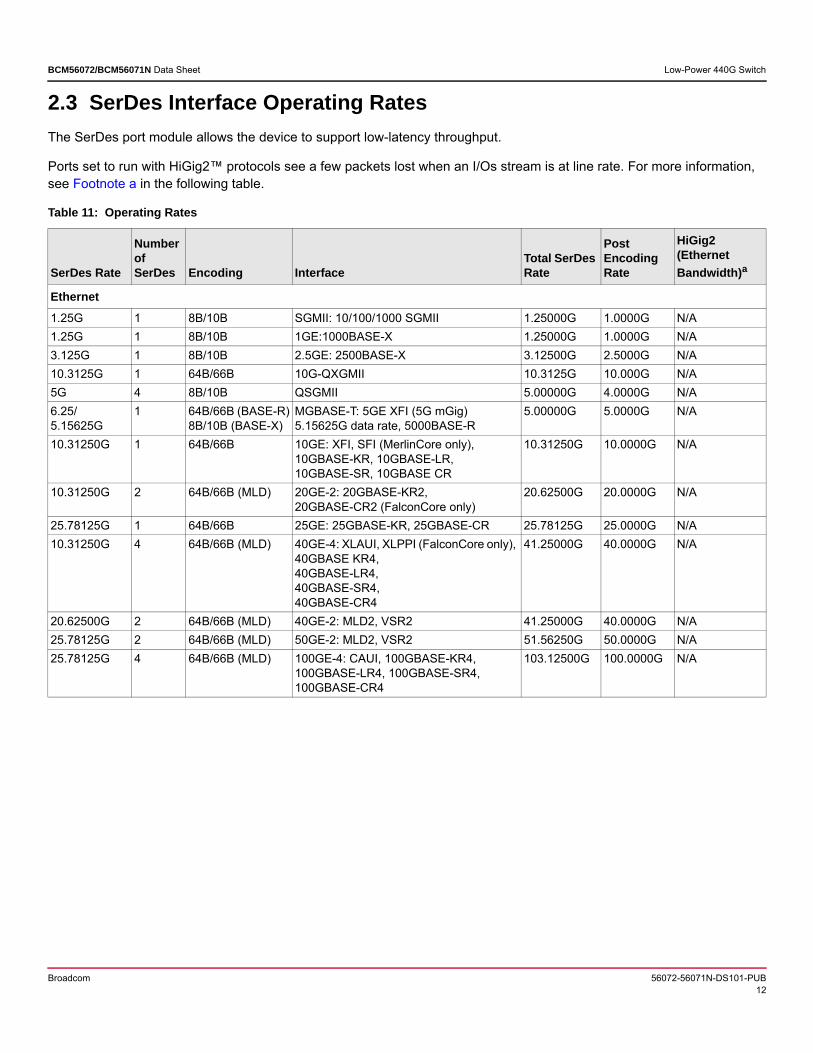
2.3 SerDes Interface Operating RatesThe SerDes port module allows the device to support low-latency throughput.
Ports set to run with HiGig2™ protocols see a few packets lost when an I/Os stream is at line rate. For more information, see Footnote a in the following table.
Table 11: Operating Rates
SerDes Rate
Number of SerDes Encoding Interface
Total SerDes Rate
Post Encoding Rate
HiGig2 (Ethernet Bandwidth)a
Ethernet1.25G 1 8B/10B SGMII: 10/100/1000 SGMII 1.25000G 1.0000G N/A1.25G 1 8B/10B 1GE:1000BASE-X 1.25000G 1.0000G N/A3.125G 1 8B/10B 2.5GE: 2500BASE-X 3.12500G 2.5000G N/A10.3125G 1 64B/66B 10G-QXGMII 10.3125G 10.000G N/A5G 4 8B/10B QSGMII 5.00000G 4.0000G N/A6.25/5.15625G
1 64B/66B (BASE-R)8B/10B (BASE-X)
MGBASE-T: 5GE XFI (5G mGig) 5.15625G data rate, 5000BASE-R
5.00000G 5.0000G N/A
10.31250G 1 64B/66B 10GE: XFI, SFI (MerlinCore only), 10GBASE-KR, 10GBASE-LR, 10GBASE-SR, 10GBASE CR
10.31250G 10.0000G N/A
10.31250G 2 64B/66B (MLD) 20GE-2: 20GBASE-KR2,20GBASE-CR2 (FalconCore only)
20.62500G 20.0000G N/A
25.78125G 1 64B/66B 25GE: 25GBASE-KR, 25GBASE-CR 25.78125G 25.0000G N/A10.31250G 4 64B/66B (MLD) 40GE-4: XLAUI, XLPPI (FalconCore only),
40GBASE KR4, 40GBASE-LR4,40GBASE-SR4, 40GBASE-CR4
41.25000G 40.0000G N/A
20.62500G 2 64B/66B (MLD) 40GE-2: MLD2, VSR2 41.25000G 40.0000G N/A25.78125G 2 64B/66B (MLD) 50GE-2: MLD2, VSR2 51.56250G 50.0000G N/A25.78125G 4 64B/66B (MLD) 100GE-4: CAUI, 100GBASE-KR4,
100GBASE-LR4, 100GBASE-SR4, 100GBASE-CR4
103.12500G 100.0000G N/A

Broadcom 56072-56071N-DS101-PUB13
BCM56072/BCM56071N Data Sheet Low-Power 440G Switch
NOTE: Broadcom-proprietary 64B/66B encoding is not supported in the Falcon (TSC4-F) SerDes core. Other legacy devices that use Eagle (TSC4-E), TSC-4, or Warpcore® support both IEEE and Broadcom-proprietary 64B/66B encoding. Therefore, when Falcon operates in a HiGig™ mode, such as HG[42] and interfacing to a legacy device, the legacy device must enable IEEE 64B/66B encoding rather than Broadcom-proprietary 64B/66B encoding.
HiGig2
10.93750G 1 64B/66B HGs[11]b 10.93750G 10.6061G 10.1234G
10.3125G 2 64B/66Bc HGd[20] 20.6250G 20.0000G 19.0900G
10.93750G 2 64B/66B (MLD) HGd[21]d 21.87500G 21.2121G 20.2469G
27.34375G 1 64B/66B HGs[27]e 27.34375G 26.5151G 25.3087G
10.93750G 4 64B/66B (MLD) HG[42] 43.75000G 42.4242G 40.4939G25.78125G 2 64B/66B (MLD) HGd[50] 51.56250G 50.0000G 47.7250G27.34375G 2 64B/66B (MLD) HGd[53] 54.68750G 53.0303G 50.6174G
a. The HiGig2 (Ethernet Bandwidth) is calculated based on the assumption of having HG_IPG = 8 bytes and a minimum payload size of 64 bytes. For example, a HG[11]-1 port will have an effective Ethernet switching bandwidth of 10.1240G. This is based on the following formula:• HG (Ethernet Bandwidth) = HG[speed] × Ethernet_Efficiency• HG[speed] = N_Lanes × Baud Rate × Encoding• Ethernet_Efficiency = (E_IPG + Preamble + E_Payload) ÷ (HG_IPG + HG_Header + E_Payload) = (12 + 8 + 64) ÷ (8 + 16 + 64) = 95.45%
b. A small amount of packet loss is observed when a port set to HGs[11] runs at line rate because only 10 Gb/s data bandwidth is allocated to the port.
c. This 64B/66B encoding is a Broadcom-proprietary implementation. Falcon supports only IEEE standard 64B/66B encoding.
d. A small amount of packet loss is observed when a port set to HGd[21] runs at line rate because only 20-Gb/s data bandwidth is allocated to the port.
e. A small amount of packet loss is observed when a port set to HGs[27] runs at line rate because only 25-Gb/s data bandwidth is allocated to the port.
Table 12: Port Terminology
Port Terms Standard Port Speed Standard TerminologyMultigigabit (mGig) IEEE802.3bz 5G, 2.5G, 1G MGBASE-T (5.0 Gb/s)Multigigabit-Lite (mGig-Lite) IEEE802.3bz 2.5G, 1G NBASE-T (2.5 Gb/s)
Table 11: Operating Rates (Continued)
SerDes Rate
Number of SerDes Encoding Interface
Total SerDes Rate
Post Encoding Rate
HiGig2 (Ethernet Bandwidth)a

Broadcom 56072-56071N-DS101-PUB14
BCM56072/BCM56071N Data Sheet Low-Power 440G Switch
2.4 Port Mode CapabilitiesThe BCM56072/BCM56071N contains three types of SerDes interfaces: the PCIe Gen3 PHY, the Merlin SerDes interface, and the Falcon SerDes interface. Each of these interfaces has different capabilities depending on the device part number and selected configuration option. This section describes the various capabilities of each SerDes interface.
2.4.1 PCIe InterfaceThe PCIe interface provided by the BCM56072/BCM56071N conforms to PCIe Gen 3.0 specifications. PCIe controller supports a single-lane endpoint configuration Root port configuration is not supported
2.4.2 Merlin InterfaceThe Merlin SerDes interfaces are primarily used for high-speed front-panel ports, up-links, or stacking ports. For operating modes in a given Merlin core, the following features are applied: Quad 10G SerDes with QSGMII/10G-QXGMII support. Supports 1 PLL per quad. 5G XFI (5.15625 Gbaud or 64/66 5 Gb/s), QSGMII, and 10G-QXGMII in multiport mode (4 × 1G and 4 × 2.5G) are
supported. XFI, SFI, XAUI, 1000BASE-X, and 2500BASE-X (8b/10b, no auto-negotiation) is supported. 10GBASE-KR, 10GBASE-LR, 10GBASE-SR, 10GBASE-CR, 40GBASE-KR4, 40GBASE-CR4, 40GBASE-LR4, and
40GBASE-SR4 interface types are supported. 20G HG+ (two lanes), 21G HG2 (two lanes), and 42G HG2 (four lanes) is supported. Single-lane FEC (Clause 74). Supports half-duplex mode for 10/100 Mb/s speed with external GPHY in QSGMII interface mode. 1G/10G (native Ethernet) or HGs[10] mix in the same SerDes supporting HGd[20]. Polarity inversion can be made on both the TD and RD paths with individual lane controls. The lane-swap capability is restricted to RD lanes in the receive path and TD lanes in the transmit path. Lane swapping
across TD and RD lanes is not supported. 1G (native Ethernet)/10G (native Ethernet or HGSolo[10]) mix in the same quad is supported. HiGigSolo[11] (HG+/HG2 packets over 10.9375-GHz lane, in other words, overclocked XFI) is supported. 1G and 10G port mix over the backplane is supported in the same quad.

Broadcom 56072-56071N-DS101-PUB15
BCM56072/BCM56071N Data Sheet Low-Power 440G Switch
2.4.3 Falcon InterfaceThe Falcon (TSC4-F) SerDes core interfaces are primarily used for high-speed up-links or stacking ports. For operating modes in a given Falcon core, the following features are applied: Clause 73 full-duplex is supported where applicable. 1000BASE-X and 2500BASE-X are supported. 100GBASE-KR4, 100GBASE-SR4, 100GBASE-LR4, and 100GBASE-CR4 are supported. 1000BASE-KX and SFI are supported, but the mix of port speeds is limited to a shared VCO. XFI, 10GBASE-KR, 10GBASE-CR, 10GBASE-LR, 10GBASE-SR, and 5000BASE-R are supported. XAUI is not supported. HGd[21], HGs[27], HG[42], and HGd[53] are supported. HGs[11] (HG+/HG2 packets over 10.9375 GHz lane, in other words, overclocked XFI) is supported. 1G/10G (native Ethernet) or HGs[10] mix in the same SerDes supporting HGd[20]. 1G/10G Ethernet mix in the same quad, concurrently. 1G/25G Ethernet mix in the same quad, concurrently. 10G/25G Ethernet mix in the same quad, concurrently. Clause 91 FEC is supported on 25G, 25G HG2, 50G, 53G HG2, 100G, and 106G interfaces. Clause 74 FEC is supported for 10G and 40G interfaces. Half-duplex is not supported. 1G, 2.5G, 10G, 25G, and 50G (MLD) Ethernet mix is supported in the same quad. Polarity inversion can be made on both the TD and RD paths with individual lane controls. The lane swap capability is restricted to RD lanes in the receive path and TD lanes in the transmit path. Lane swapping
across TD and RD lanes is not supported.
NOTE: 5G and 25G cannot operate within the same port macro.

Broadcom 56072-56071N-DS101-PUB16
BCM56072/BCM56071N Data Sheet Low-Power 440G Switch
2.5 Feature ListThe feature list in the following table applies to the BCM56072/BCM56071N.
Table 13: Feature List
Feature DescriptionInterfaces PCIe Gen3 1-lane.
16 GPIOs. UART. JTAG. BroadSync. Serial LED for network ports. MDC/MDIO. QSPI, SPI, and I2C. Sixteen 25G SerDes (four Falcon cores, four lanes per core).
– Flexible SerDes contains four SerDes lanes per Falcon core, configured to operate in any of the following configurations: 10GbE XFI, SFI, KR, CR, SR, and LR (CL74) (1-lane). 20GbE KR2 (CL74) (2-lane). 25GbE KR1 and CR1 (CL74, CL108) (1-lane). 40GbE MLD2 and VSR2 (2-lane). 40GbE XLAUI, XLPPI, KR4, CR4, SR4, ER4, and LR4 (CL74) (4-lane). 50GbE MLD2 and VSR2 (2-lane) CL108. 100GbE KR4, CR4, SR4, ER4, and LR4 (CL91 FEC) (4-lane). MLD HiGig2 HG[42] and HG[53] (CL74) (4-lane)
Twelve 10G SerDes (three Merlin cores, four lanes per core).– Flexible SerDes contains four SerDes lanes per Merlin Core, configured to operate in any of the following
configurations: 10/100 BASE-X. 1000 BASE-X. 2500BASE-X. 10GbE XFI, SFI, KR, CR, SR, ER, and LR (CL74) (1-lane). 20GbE KR2 (CL74) (2-lane). 40GbE MLD2 and VSR2 (2-lane). 40GbE XLAUI, XLPPI, KR4, CR4, SR4, ER4, and LR4 (CL74) (4-lane). MLD-HiGig2 HG[42] (CL74) (4-lane). QSGMII. 10G-QXGMII.
Integrated Processors 4 Cortex M0 and 2 R5 CPU.Flexible Port Configurations
12 × 10GE + 6 × 50GE or 12 × 25GE. 48 × 2.5GE + 6 × 50GE or 12 × 25GE. 20 × 10GE 1 × 100GE + 2 × 100GE. 2 × 100GE + 2 × 100GE (bump-in-the-wire). 28 × 10GE or 7 × 40GE. 40 × 1GE + 8 × 2.5GE + 2 × 25GE + 10 × 10GE. 48 × 1GE + 6 × 50GE or 12 × 25GE.

Broadcom 56072-56071N-DS101-PUB17
BCM56072/BCM56071N Data Sheet Low-Power 440G Switch
MAC Characteristics Supports:– Ethernet/IEEE 802.3 frame sizes (64 bytes to 1522 bytes).– Jumbo frames up to 12,288 bytes.– EEE.
Supports IEEE 802.1AS, pre-standard IEEE 802.1AS-Rev, IEEE 1588, and IEEE 1588v2-2008 network time distribution:– IEEE 1588 and pre-standard 802.1AS-Rev.– Transparent clock (TC), boundary clock (BC), and ordinary clock (OC).– Supports SyncE layer-1 clock recovery.
802.3ad Link Aggregation
128 trunk groups supported with up to eight members per group. No adjacency limitation. Traffic load distribution for L2 switched and L3 routed packets. Trunk port selection based on a hash on source or destination MAC, VLAN, EtherType, source or destination
IP address, and TCP or UDP ports. Trunk port selection for DLF, broadcast, and multicast packets.
HiGig Trunking Eight HiGig trunk groups supported with up to eight members per group. HiGig trunk failover supported. VLANs Supports 4K VLAN assignment for untagged and priority tagged packets based on the following:
64 IP subnet-based VLANs. 16 protocol-based VLANs. 1K MAC-based VLANs. 256 flow-based VLAN. IEEE 802.1p. IEEE 802.1Q ingress port.Additional VLAN features include the following: Independent VLAN learning (IVL) and shared VLAN learning (SVL). Ingress filtering for IEEE 802.1Q VLAN security. VLAN-based packet filtering. VLAN translation on ingress and egress. VLAN Cross-connect. Private VLANs. VLAN counter pool (ingress):
– 256 counters in the shared pool.– Indexed by ingress VLAN translation table action.– Indexed by VFP action.
VLAN counter pool (egress): – 256 counters in the shared pool.– Indexed by egress VLAN translation table action.
VLAN Range-Based Double Tagging (Matching)
Allows a range of CVIDs to be mapped into the same SPVID without consuming multiple entries in the VLAN translation table.
Supports 128 VLAN range profiles. Each VLAN range profile has a set of eight VLAN ranges configurable by software.
VLAN Double Tagging Support for IEEE 802.1ad provider bridging: Unqualified learning and forwarding. Ability to add, remove, and translate (replace) both the service-provider VLAN tag and customer VLAN tag. Support for four, programmable outer TPIDs with non-overlapping VLANs. Support for double tagging requirements of Broadband Forum TR-101. Packet forwarding is supported based on: S-VLAN bridging: L2 switch based on MAC_DA and S-VID. S-VLAN cross-connect: Destination port is based on S-VID only. Double VLAN cross-connect: Destination port is based on (S-VID, C-VID) combination. Support for 2K shared (S-VID, C-VID).
Table 13: Feature List (Continued)
Feature Description

Broadcom 56072-56071N-DS101-PUB18
BCM56072/BCM56071N Data Sheet Low-Power 440G Switch
Spanning Tree Spanning tree support includes the following: 128 counters in the shared pool. IEEE 802.1D spanning tree protocol (single spanning tree per port). IEEE 802.1s for multiple spanning trees. IEEE 802.1w rapid spanning tree protocol – delete and/or replace per port, per VLAN. Spanning tree protocol packets detected and sent to the CPU.
32-bit Custom Header support
32-bit custom header addition after MAC source address in an Ethernet packet (Channelized Flow Control and Forwarding).
32-bit custom header removal after MAC source address in an Ethernet packet. 32-bit custom header replacement after MAC source address in an Ethernet packet. Custom header based forwarding (channelized forwarding). 128 custom headers (1024 with OAM disabled).
L2 Unicast Supports the following: Learning up to 16K MAC addresses. 16K static entries. 64 user entries. Line rate switching for all packet sizes. Shared and independent hardware VLAN learning. VLAN flooding for broadcast and DLF packets. Hardware-based address learning. TCAM to learn up to 64 MAC addresses encountering hash collision. Hardware- and software-based aging. Software insertion, deletion, and lookups of the L2 table. Same port bridging supported. Class based learning (station movement control). Supports MAC learn limits per source port (trunk), per VLAN, and per VFI.
L2 Multicast Supports 1K L2 multicast groups. Line rate switching for all packet sizes. Three port-filtering modes to control multicast packet behavior.
IGMP snooping IPv4 IGMP (v1, v2, v3) snooping without tunnels. IPv6 MLD snooping without tunnels.
Provider Backbone Bridging
MAC-in-MAC Lite with limited support for initiation and termination of, at most, 64 IEEE 802.1ah compliant MAC-in-MAC tunnels: Parsing MAC-in-MAC. Forwarding decision based on outer MAC header B-SA, B-DA, BVID, ISID in IFP. Configurable backbone service instance tag (EtherType) classification based on I-Tag TCI.
Table 13: Feature List (Continued)
Feature Description

Broadcom 56072-56071N-DS101-PUB19
BCM56072/BCM56071N Data Sheet Low-Power 440G Switch
Layer-3 Routing (IPv4, IPv6)
IPv4 or IPv6 hosts line rate routing for all packet sizes and conditions. Supports: Up to 512 directly-attached hosts in the L3 table. Up to 64 longest prefix match (LPM) based routing. 512 next hops 128 Layer-3 interfaces Up to 16 partitions of routing tables (VRF) based on ingress port, VLAN, or flow type. Unicast reverse path forwarding (uRPF) to limit malicious traffic.Software-based aging support. 64 ECMP groups.ECMP hash-selection mechanisms: Legacy hash-selection mechanisms. IP + UDP + BTH header-based hash for Routable RDMA over Converged Ethernet (RRoCE), and also L2
RRoCE. L2 + VXLAN header-based hash for VXLAN-Lite implementation.
IP Multicast Up to 128 IPMC groups. Multicast packet replication support for up to 1K VLANs. Line-rate operation for all packet sizes and conditions. Simultaneous L2 bridging and L3 routing. Optional source port and VLAN checks. Lookup: S, G, V and *, G, V IM-SM, PIM-DM, PIM-SSM, and DVMRP on a per VLAN basis. Reverse path forwarding checks. Ability to fall back to L2 multicast lookup on an IPMC miss. Filter Mode (PFM) per VLAN for L2 multicast, IPv4 multicast, and IPv6 multicast packets. Control trapping of unknown IPMC packets to CPU on a per VLAN per IP type basis. IP multicast address consistency check with destination MAC address.
MAC-IP binding Hardware support for checking source IP and source MAC address combinations (binding) in IPv4 ARP and RARP packets.
Tunnel Encapsulation and Deencapsulation
IP tunnels: VXLAN-Lite. VXLAN-Lite: VTEP – Limited end-point support for, at most, 128 VXLAN tunnels (VFIs). VXLAN transit: parsing of VXLAN header-based limited ACL and QoS support and ECMP-based load
balancing of VXLAN packets passing through the switch. ACL and QoS using IFP. Multiple MAC addresses mapping to one VFI.
Table 13: Feature List (Continued)
Feature Description

Broadcom 56072-56071N-DS101-PUB20
BCM56072/BCM56071N Data Sheet Low-Power 440G Switch
ContentAware™ Processing (Ingress Field Processor)
1K Single-wide rules. Layer 2 through 7 packet classification. Intelligent protocol-aware processor with backward compatible byte-based classification option. Parses up to 128 bytes per packet. Multiple lookups per packet. Supports:
– Multiple matches and actions per packet. – ACL-based policing. – Ingress port-based filtering. – MAC destination address remarking.– Class-based marking for SLAs. – Traffic-class definition based on the filter. – Classification of different packet formats (IPv6, IPv4, double tagged, HTLS, IEEE 802.1Q, Ether II,
IEEE 802.3). Hierarchical min/max programmable meters allows policing of flows. Dual-leaky bucket meters support two-rate three-color marking. srTCM, trTCM, and modified trTCM
(RFC2697, RFC2698, RFC4115). Metering support on ingress ports and CPU queues. Jumbo packet metering. TCP and UDP port number range checking. IPv6 filtering (128 bits). Filtering IP packets with options. Modified srTCM support in ingress field processor (IFP) meters (consume green + yellow tokens for frames
marked yellow). Also known as TSN metering. Minimum 250 b/s service metering granularity.
VLAN Field Processor (VFP)
256 single-wide rules. Flexible VLAN assignment, for untagged and tagged packets, based on L2 through L4 field processing. Q-in-Q feature capability includes modifications to fields within inner or outer tags. Single-wide, or double-wide modes. Field selectors on per-port, per-slice, and per-packet-type basis. Ability to add or replace VLAN tag, change priority, assign classification-ID, or drop.
ContentAware Processing (Egress Field Processor)
256 single-wide rules. Filter on fully modified packets allowing egress ACLs. Filter on modified L3 routed and IPMC replicated packets. Keys based on L2 through L4 fields for IPv4 and IPv6 packets. Actions: drop, change DSCP, change inner or outer priority, change inner or outer VLAN ID, change outer
and TPID. Byte-based and packet-based statistics. Egress metering (policing): Flow mode, srTCM, trTCM, modified trTCM. Modified srTCM support in egress field processor (EFP) meters (consume green + yellow tokens for frames
marked yellow). Also known as TSN metering. Minimum 250 b/s service metering granularity.
Table 13: Feature List (Continued)
Feature Description

Broadcom 56072-56071N-DS101-PUB21
BCM56072/BCM56071N Data Sheet Low-Power 440G Switch
Quality of Service Eight CoS queues per port. 64 CoS queues per port (up to 8 ports). Enhanced eight CoS queues for CPU. Three drop precedence colors. Per port, per CoS drop profiles. Minimum/maximum bandwidth guarantee (shaping) per CoS, per port. Traffic shaping available on CPU queues: bandwidth based and packets- per-second based. Programmable priority to CoS queue mapping. Provides two levels of drop precedence per queue. Explicit Congestion Notification (ECN) for congestion avoidance. Strict Priority (SP), Weighted Round Robin (WRR), and Deficit Round Robin (DRR) mechanism for shaped
queue selection. Programmable bucket size of egress port shaping and CoS shaping. Support for ingress port rate based policing and pause flow control. Mapping of incoming priority, CFI to outgoing priority and drop precedence.
DSCP Per-port DSCP remarking. DSCP remarking based on a FP filter match. DSCP-to-802.1p mapping. Remap incoming DSCP to new outgoing DSCP.
Memory Management Unit (MMU)
Integrated 2 MB of total packet buffer. Cut-through switching for low pin-to-pin latency. Static memory allocation. Programmable transmit queue thresholds. Programmable ingress per-port and queue thresholds. Ingress cell triggers for backpressure. Cell and packet thresholds for triggering head-of-line (HOL) prevention. Error correction on control header and packet buffer. Software TCAM soft error rate (SER) protection.
Queue Structure Network interfaces with single-level unicast (UC) and multicast (MC) queues. Eight network ports, at most, with optional two-level queues for UC and MC packets.
Storm Control Four meters for packet-based or byte-based rate control with the following packet types: Unknown unicast (DLF) packet rate control. Broadcast packet rate control. Known L2MC packets rate control. Unknown L2MC packets rate control. Known IPMC packets rate control. Unknown IPMC packets rate control.
Table 13: Feature List (Continued)
Feature Description

Broadcom 56072-56071N-DS101-PUB22
BCM56072/BCM56071N Data Sheet Low-Power 440G Switch
Scheduling Per-port one-level scheduling.NOTE: 52 logical network ports have one level scheduler. Hierarchical two-level schedulers are on eight logical network ports where the scheduling discipline on both levels is the same. Scheduling discipline support in port-level scheduler. SP WRR DRR DRR + SPScheduling discipline support in leaf-level scheduler in two-level scheduler. SP WRR DRR DRR + SP
Congestion Management
Support for multiple congestion notification formats within the system. PAUSE messaging. Priority-based Flow Control (PFC) in the first (port) level scheduler in a two-stage scheduler. HiGig pause. Service Aware Flow Control (SAFC) messages. Channelized PAUSE/PFC forwarding over Ethernet. Channelized End-to-End Congestion Control (E2ECC) over Ethernet. End-to-End Congestion Control (E2ECC) on HiGig2. End-to-End Flow Control (E2EFC) on HiGig2. ECN.
Denial-of-Service (DoS) Attack Prevention and Protocol Checkers
Built-in illegal address check (IPv4 and IPv6). DoS detection and prevention. Land packets (SIP = DIP). NullScan (TCP sequence number = 0, control bits = 0). Ping flood (of IPMC packets). SYN and SYN-ACK flooding. SYN with sPort < 1024. Smurf attack. Individual control over handling of DoS packet.
Flow Control PAUSE/PFC support. Channelized PAUSE/PFC support. End-to-End congestion control (E2ECC).
IPG Stretching Enables control of the transmitted packet data rate by altering IPG. Supports 2.5G and 5G data rates over 10G XFI links.
Management Information Base
sFlow support, RFC 3176. Remote monitoring (RMON) statistics group, IETF RFC 2819. Simple network management protocol (SNMP) interface group, IETF RFC 1213, 2836. Ethernet-like MIB, IETF RFC 1643. Ethernet MIB, IEEE 802.3u. Bridge MIB, IETF RFC 1493.
Table 13: Feature List (Continued)
Feature Description
Broadcom 56072-56071N-DS101-PUB23
BCM56072/BCM56071N Data Sheet Low-Power 440G Switch
Mirroring One instance of Ingress/egress mirroring support. A separate packet is created for each mirror-to-port (MTP) port. Mirror-to-port receives unmodified packet for ingress mirroring. Mirror-to-port receives modified packet for egress mirroring. Mirroring across stacked modules. Number of MTP supported is one for both ingress and egress mirroring. Mirror-to-port can be a link aggregation group. Remote Switched Port Analyzer (RSPAN) mirroring, VLAN mirroring, and flow mirroring. Encapsulated Remote Switched Port Analyzer (ERSPAN) mirroring.
Port Extender Supports 6-byte VNTAG. Supports 8-byte E-TAG (IEEE 802.1BR).
Virtualization Storage L2VPN for L2 services using MAC in UDP. Storage RRoCE.
RRoCE transit: RRoCE transit – Limited support for IPv4 or IPv6 RRoCE v1 and v2 packets passing through the switch. IPv4 and IPv6 RRoCE. ECMP using RRoCE V2 BTH. LAG using RRoCE V1/V2 headers. ACL and QoS using IFP.
Ethernet OAM Link-Level OAM, IEEE 802.3ah, Clause 57. Supports IEEE 802.1ag connectivity fault management solution, including hardware CCM transmission,
CCM fault monitoring, and loopback reply. ITU-T Y.1731 on-demand/proactive loss measurement and one-way/ two-way delay measurement. DownMEP in hardware. 512 LMEP. 2048 RMEP.
Time Sensitive Networking (TSN) (only supported on industrial-version parts)
Seamless Redundancy supported: – Support for HSR (IEC 62439-3), PRP (IEC 62439-3), and IEEE 802.1CB. – HSR-2-PRP conversion is not supported in the Falcon cores when they are set up in 25G mode. – Proxy support for end node. – Cut-through and seamless redundancy support for HSR and IEEE 802.1CB frames. – Support for protocol-specific modes. – Coupler support. – Configurable sliding and acceptance windows (per flow). – Sequence window aging. – Seamless redundancy control and management packet redirection to CPU. – Hardware learning of flows for HSR and PRP.
Time-aware per-stream filtering and policing: – Support for IEEE 802.1Qci. – 64 gates for time aware per-stream filtering.– 16 waveform transitions per gate. – IFP- and EFP-based ingress and egress flow meters supporting srTCM, trTCM, modified srTCM, and
TSN. – Additional 256 ingress service meters supporting srTCM, trTCM, modified srTCM, and TSN metering.
Time-aware scheduling: – Support for IEEE 802.1Qbv. – Supported on all ports. – Eight priorities per port, which can be time-aware scheduled.– 128 waveform transitions per port.
Table 13: Feature List (Continued)
Feature Description

Broadcom 56072-56071N-DS101-PUB24
BCM56072/BCM56071N Data Sheet Low-Power 440G Switch
TSN (Continued) Timing synchronization: – Support for IEEE 1588, 802.1AS Rev on all ports. – 1-ns timestamp accuracy on Falcon ports. – Dual-zone (global clock and working clock). – Hardware generated pDelay burst. – Equal (similar) latency forwarding SYNC messages to multiple egress port. – Hardware time-of-day (ToD) counter to drive time-aware scheduler. – Hardware-generated 1 PPS output.
General purpose checks and counters: – MTU size check on profile base, per port STU and MTU check, per-TSN stream. – STU/MTU check and per-queue STU/MTU check. – 32-bit width IFP- and EFP-based ingress and egress flow counters. – Additional 32-bit wide 1K ingress and 256 egress flexible flow counters.
Cyclic queuing and forwarding (IEEE 802.1Qch).– Time-aware stream filtering and policing IEEE 802.1Qci.– Time-aware scheduling IEEE 802.1Qbv.
Hash Enhancements RTAG-7 flow-based hashing. VXLAN ECMP Hashing. IP + UDP + VXLAN. RRoCE v1 Lag Hashing. L2 MAC + BTH. RRoCE v2 ECMP Hashing. IP + UDP + BTH header.
Port Security Supports 802.1x. Blocking of egress ports on per ingress port or LAG basis (source port filtering). Blocking of egress ports on per MAC address basis. Blocking of egress ports for broadcast, unknown unicast, and multicast packets.
Stacking Links Supports L2 and L3 across stacked modules. L2MC and IPMC support across stacked modules. VLAN membership supported across stacked modules. Seamless CoS support. Mirroring and remote mirroring support. Supports up to 256 stacked modules. Trunking of stacking ports. ContentAware processing on stacking port.
Table 13: Feature List (Continued)
Feature Description

Broadcom 56072-56071N-DS101-PUB25
BCM56072/BCM56071N Data Sheet Low-Power 440G Switch
2.6 MemoryThe BCM56072/BCM56071N device integrates all table memory necessary to support its functions. The following table indicates the major internal table memory allocations and their functions for switching, routing, and classification.
Table 14: Switch Internal Memory Table
Table Name Size FunctionPort One entry per front-panel,
stacking, channelized, and CPU port
Per-port configuration settings and attributes. For example, L2 learning, port discards, VLAN handling, and priority assignment.
Subnet-Based VLAN 64 Assigns VLAN, based on source IP subnet for untagged, and priority-tagged packets.
MAC-Based VLAN Shared 1024 Assigns VLAN based on source MAC address for untagged and priority-tagged packets (shared).
MAC-IPv4 Shared 1024 Checks the IPv4-MAC binding of IP packets as well as ARP/RARP request/reply messages for sender IPv4-sender MAC address binding (shared).
VLAN Translation (Ingress) Shared 1024 Translates VLAN between customer VLAN and service provider VLAN for provider bridging (shared).
VLAN Translation (Egress) 1024 Translates VLAN between customer VLAN and service provider VLAN for provider bridging.
Protocol-Based VLAN 16 Assigns VLAN based on packet protocol for untagged, and priority-tagged packets.
VLAN Table 4K Indicates port membership and spanning tree group for each VLAN.DSCP Table Ingress: 4224
Egress: 4224Remaps ingress and egress DSCP to new DSCP and priority.
Spanning Tree Group 128 Indicates spanning tree state for each port for each spanning tree group.MAC Address(L2 Stations)
16K Contains learned and programmed MAC addresses: indicates the destination port and additional properties of each MAC address. For example, source/destination discard, priority, blocking, or mirroring.
Reserved MAC Address(L2 User Entries)
128 Contains reserved MAC addresses, programmed by software for special handling. For example, copy to CPU, drop, flood, for control packets, BPDUs.
Layer 2 Multicast 1K Indicates port membership for Layer 2 multicast groups.Link Aggregation Group 128 Indicates port membership of link aggregation groups and hash selection
criteria.Maximum Ports per Trunk Group
8 —
HG Trunk Groups 8 —My Station Table 32 Used for all my station checks, such as routed traffic.Layer 3 Host Route 512 IPv4
256 IPv6 Contains host IPv4 and IPv6 addresses for Layer 3 host routing, used as ARP cache.
Layer 3 LPM Route 64 IPv432 IPv6
Contains IPv4 and IPv6 subnets for longest prefix match routing, including ECMP/WCMP routing.
Layer 3 IP Multicast 256 IPv4128 IPv6
Indicates port membership for Layer 3 IP multicast (S, G) or (*, G) lookups, and controls replication of IPMC packets on egress ports with multiple VLANs.
Layer 3 VRF 16 Number of VPN segmentation of L3 routing tables. Each VPN ID assigned based on ingress port, VLAN, or flow.
ECMP Groups 64 L3 Equal Cost Multipath table.

Broadcom 56072-56071N-DS101-PUB26
BCM56072/BCM56071N Data Sheet Low-Power 440G Switch
ECMP Members per Group 64 —Layer 3 Tunnel 128 IPv4
64 IPv6Contains configuration of VXLAN-Lite tunnels, for example, tunnel type, destination/source IP address.
VLAN ContentAware Processor 256 rules; 4 slices Rules for assignment of VLAN, based on flexible criteria, block packets, bind MAC address with IP address, and assign VPN ID.
Ingress ContentAware Processor
1K rules8 slices232 bits Key Depth
Rules for L2 through L7 packet classification on ingress, ACLs, metering, statistics.
IFP Meters 1K Number of token buckets.IFP Counter 1K Per-slice counters for packet and byte.Egress ContentAware Processor
256 rules4 Slices214 bits Key Depth
Rules for packet classification on egress, ACLs, metering, and statistics.
EFP Meters 256 Number of token buckets.EFP Counter 256 —Service Meters 256 Number of token buckets.
Table 15: Operations, Administration, and Maintenance (OAM) Table
Table Name Size FunctionLMEP 512 For generating hardware CCM packets.LMEP DA 512 For generating hardware CCM packets.L3 Entry IPv4 Unicast 2K MP group lookup table shared with IPv4 unicast route entry table.MA Index 4K Provide session ID for each MEP and the opcode profile pointer.MAID Reduction 512 Compare the reduced MAID from the packet to the configured value in the table.MA State 512 Track the state of the local MEP for CCM packets.RMEP 2K Track the state of the remote MEP for CCM packets.OAM Opcode Control Profile 16 For action control defined for processing each opcode.OAM LM Counter 4K Counters for OAM loss measurement.
Table 16: Device Scalability
Table Name SizeIntegrated Packet Buffer Memory 2 MB Maximum of logical ports with large number of XQs.NOTE: An XQ is a packet pointer data structure with the starting address of the buffer where the packet is stored. Each port has a dedicated XQ memory that contains pointers of all stored packets in all active queues of the port. The size of XQs in a port limits the maximum number of stored packets that are waiting to be transmitted on that port. NOTE: A logical port can be mapped to a physical port through configuration.
8
Number of logical ports with smaller number of XQs. 52XQs for the CPU port. 2048Number of entries in large XQs 6144Number of entries in smaller XQs 2048
Table 14: Switch Internal Memory Table (Continued)
Table Name Size Function

Broadcom 56072-56071N-DS101-PUB27
BCM56072/BCM56071N Data Sheet Low-Power 440G Switch
Table 17: Single-Level Queue Structure
Table Name SizeNumber of network interfaces with single-level UC/MC queues (Merlin, Falcon, and PM4x10Q)One logical port can be mapped to one of the external physical network interfaces (except for two internal ports) through device configuration.
52
Number of queues per CoS 1Number of CoS per network or HiGig port 8TSN Time-Aware Scheduling (TAS) enable YesTSN seamless redundancy Yes
Table 18: Two-Level Hierarchical (HQOS) Structure
Table Name SizeNumber of logical ports with additional two-level UC/MC queues (Merlin and Falcon) 8Number of queues per CoS 8IFP based queue assignment for 64 queues per port with two-level scheduler YesNumber of CoS per network or HiGig port 8TSN Time Aware Scheduling (TAS) enable NoTSN seamless redundancy No
Table 19: Seamless Redundancy Tables
Table Name Note SizeNumber of seamless redundancy flows MAC-SA 256
MAC-DA, VLAN, PRI 256SA + DA + VLAN + SIP + DIP + Protocol + S-Port + D-Port (VFP based)
VFP based: 1 VFP rule per flow
Number of bits in the sequence number HSR (IEC 62439-3)/ PRP (IEC 62439-3)/IEEE 802.1CB
16 bits
Number of L2 Entry (MAC address) support with Seamless Redundancy HSR (IEC 62439-3)/ PRP (IEC 62439-3)/IEEE 802.1CB
16K
Number of MTU profiles — 16Number of sets of ingress port counters per port HSR (IEC 62439-3)/
PRP (IEC 62439-3)/IEEE 802.1CB
Standard based
Number of sets (each set has 1K counters) of ingress flow counters as per HSR/PRP/1CB standards or customer requirements
HSR (IEC 62439-3)/ PRP (IEC 62439-3)/IEEE 802.1CB
8
Number of sets of egress port counters per port HSR (IEC 62439-3)/ PRP (IEC 62439-3)/IEEE 802.1CB
4
Number of sets (each set has 1K counters) of egress flow counters as per HSR, PRP, or 1CB standards or customer requirements
HSR (IEC 62439-3)/ PRP (IEC 62439-3)/IEEE 802.1CB
2
Broadcom 56072-56071N-DS101-PUB28
BCM56072/BCM56071N Data Sheet Low-Power 440G Switch
2.7 Target ApplicationsThe BCM56072/BCM56071N is targeted for enterprise and connectivity applications.
2.7.1 Enterprise Line Card ApplicationBCM56072/BCM56071N can operate as a line card in a Centralized Ethernet Switching (CES) system.
CES systems are typically implemented in a chassis-based solution that have line cards that serve as port fan-out switches and provide subtending ports (sub-ports or channel number) to expand the connectivity of the chassis.
In the following figure, the BCM56072/BCM56071N devices can support four different sub-port configurations: 48 × 1G 12 × 10G 48 × 2.5G
Assuming that the control bridge (CB) is a BCM56470 device, the system can be expanded with eight line cards, resulting in a maximum of 384 sub-ports facing the access domain.
Figure 2: BCM56072/BCM56071N as an Enterprise Line Card
Each line card is connected to a control bridge through a high-bandwidth Ethernet interface called the backplane port.
In port fan-out mode, the BCM56072/BCM56071N adds channelized sub-ports to the control-bridge switch. In a centralized chassis solution, the backplane ports are treated as internal data bus and are transparent to the user. This makes the chassis system behave like a single switch.
Number of service meters indexed by TSN_CIRCUIT_ID or SR_FLOW_ID
HSR (IEC 62439-3)/ PRP (IEC 62439-3)/IEEE 802.1CB
256
Maximum number of express queues/port support in hardware IEEE 802.1Qbv, IEEE 802.1Qbu 8
Table 19: Seamless Redundancy Tables (Continued)
Table Name Note Size
CB
BCM56072(Line Card-0)
Acce
ss P
orts
Net
wor
k Po
rts
Back
plan
e Po
rts
BCM56072(Line Card-1)
BCM56072(Line Card-6)
BCM56072(Line Card-7)

Broadcom 56072-56071N-DS101-PUB29
BCM56072/BCM56071N Data Sheet Low-Power 440G Switch
Chapter 3: System Functional Blocks
3.1 HiGig2 SupportThe BCM56072/BCM56071N supports the Broadcom-proprietary HiGig2 protocol. Depending on the port configuration, this can be up to two HGd[53] ports. These ports connect multiple devices to form one logical device, also known as stacking.
When a port is configured as a HiGig2 port, the configured lanes on the SerDes core are aggregated to form the port, or in some cases only a single lane is used to form the port. When these ports are used for stacking purposes, lane behavior is as follows: The lanes on the SerDes typically connect directly to another device on the same board. The lanes are brought out to a connector on a backplane for chassis applications or brought out to a front-panel port to
be used with copper cables to build the stack.
The SerDes cores used for the HiGig2 interfaces contain the necessary differential transmitter and receiver logic to allow the stack to be built without any external active logic.
3.1.1 HiGig2 Frame StructureThe HiGig2 protocol replaces the HiGig protocol. HiGig2 allows additional stacking information to be carried, such as virtual port-related information. The HiGig port must operate at 13 Gb/s to be able to carry traffic from twelve 1 Gb/s ports using the HiGig2 protocol, due to the additional 4-byte per packet overhead.
Additionally, for packets that ingress with a VLAN tag present, the tag is moved into the HiGig2 header (for certain types of flows) when going between modules. This means that the packet is four bytes shorter when going over a HiGig link. For untagged packets, the default VLAN is carried in the HiGig2 header, and no change is made to the length of the packet. Packets egress from the destination module with all of the stacking-related information removed.
3.2 Energy Efficient EthernetEnergy Efficient Ethernet (EEE) combines the MAC with a family of PHYs that support operation in low-power mode as defined by the IEEE 802.3az EEE Task Force. Low-power mode enables both the send and receive sides of the link to disable some functionality for power savings when lightly loaded, supporting a protocol at the PHY layer to coordinate transition to and from a Lower-Power-Idle (LPI) state. The transition to and from this state is transparent to upper layer protocols and applications. The BCM56072/BCM56071N implements only the MAC layer of the EEE requirements. EEE-compatible external PHYs must be used to support EEE ports.
3.2.1 EEE Control PolicyControl policy is the decision-making policy with regard to when and how long the device is to spend in the LPI state. A set of conditions must be satisfied before the PHY can be placed in a low-power state and is maintained by the EEE policy engine based on the TX and RX control policies. The goal is to optimize power savings while simultaneously minimizing the impact on switch performance.
The MAC exits the low-power state whenever it receives a single packet destined to the interface in the low-power state. The IEEE RX control policy is for the RX interface, and EEE statistics are maintained to provide power-savings metric and enable debug.
Broadcom 56072-56071N-DS101-PUB30
BCM56072/BCM56071N Data Sheet Low-Power 440G Switch
3.2.2 EEE-Related Register Controls and StatisticsThe control policy registers include the following timers: Delay-entry timer. Wake-transition timer. In addition to the aforementioned controls, EEE statistics are provided to enable tuning of the
control policy and provide the end user with the ability to quantify EEE savings.
3.3 IEEE 1588The BCM56072/BCM56071N is a highly integrated device with many hardware hooks for designs that require network time synchronization. The following features make the device ideally suited for time-synchronization applications complying with IEEE 1588: Supported modes:
– 1-step end-to-end (E2E) and peer-to-peer (P2P) transparent clock (TC), and 2-step E2E and P2P TC.– Support for transparent clock unit mode.– Support for ordinary clock (OC) slave with clock recovery1.
One-step clock features:– On-the-fly egress packet modification including UDP checksum updates and CRC updates.– All modifications to Correction Field are handled in hardware with a very short residence time.– All packets time are stamped on ingress. The clock uses switch packet processing engines to identify IEEE 1588
packets. Two-step features:
– The CPU generates the IEEE follow-up messages for the Sync and Delay using the timestamp captured in the per-port egress FIFO.
– All packets are time stamped on ingress. The clock uses switch packet processing engines to identify IEEE 1588 packets and can trap to the CPU.
Synchronizable timestamp counter:– Can be phase-locked to an external source.– BroadSync (timecode + event clock) interface.– Time-stamped GPIOs.
1. A separate SW component is necessary for OC.

Broadcom 56072-56071N-DS101-PUB31
BCM56072/BCM56071N Data Sheet Low-Power 440G Switch
3.3.1 Hardware Support for Peer-to-Peer Pdelay_Req MessagesThe IEEE 1588 architecture for this device adds the ability for the pipeline to respond to IEEE 1588 P2P Pdelay_Req messages.
3.3.1.1 Feature List
The device supports the following P2P Pdelay_Req message features: P2P Pdelay_Req message reply in hardware One-step clocking Ethernet-based Zero, one, or two VLAN tags
The generation of Pdelay_Req frames and the reception of Pdelay_Resp frames remains in software.
3.3.1.2 Functional Description
The following figure shows the steps for sending and receiving a Pdelay_Req message and the corresponding Pdelay_Resp message. The steps are as follows:
1. Clock A stores timestamp t1 when sending Pdelay_Req.
2. Clock B records timestamp t2 when receiving Pdelay_Req.
3. Clock B records timestamp t3 when sending Pdelay_Resp.a. requestReceiptTimestamp = 0.b. correctionField = correctionField + t3 – t2.c. (For one-step clocks) Clock B sends a new correctionField in Pdelay_Resp.
4. Clock A records timestamp t4 when receiving Pdelay_Resp.
5. Clock A calculates meanPathDelay.meanPathDelay = ((t4 – t1) – correctionField) ÷ 2.
Figure 3: Pdelay_Req/Pdelay_Resp Message Flow

Broadcom 56072-56071N-DS101-PUB32
BCM56072/BCM56071N Data Sheet Low-Power 440G Switch
In a functioning system, both switches at either end of a P2P link will act as both Clock A and as Clock B, both sending Pdelay_Req frames and responding to Pdelay_Req frames.
A Pdelay_Req frame is responded to by the first StrataXGS switch it encounters. It is not sent over HiGig ports.
3.4 Thermal MonitorThe BCM56072/BCM56071N device has three onboard temperature monitors. These monitors enable temperature measurements to be obtained at the die.
The thermal monitors are controlled by a common microprocessor-accessible register that resides in the TOP block.
3.4.1 Ports Register Associated with the Thermal MonitorTo access the temperature data, use the TOP_TMON[1:0]_RESULT registers.
Each TOP_TMON_RESULT register returns two fields for each of the thermal monitors: the current temperature data and the valid bit.
The temperature is derived by reading the result register and running through this formula: T = 457.99 – (0.5501 × TEMP_DATA)
The units are in Celsius.
The host processor is not required to read the TOP_TMON_RESULT registers during typical device usage. The BCM56072/BCM56071N device transmits the temperature data to the Merlin SerDes automatically. It is expected that thermal monitors are brought out of power-down and reset before the Merlin SerDes cores are enabled. The initial SerDes software is intended to make use of the temperature data at power-up, so the temperature monitor should be in a stable state before enabling the SerDes.
Table 20: Thermal Monitor Registers
Thermal Register Description Register NamePer-monitor registers Temperature data can be read from each thermal monitor
using a per-monitor register.TOP_TMON[1:0]_RESULT

Broadcom 56072-56071N-DS101-PUB33
BCM56072/BCM56071N Data Sheet Low-Power 440G Switch
Chapter 4: System Interfaces
4.1 OverviewThe major external interfaces are listed in the following table, and the sections that follow provide additional details on certain interfaces.
Table 21: System Interfaces
Interface ImplementationQSPI (iProc) One QSPI used by the iProc CPU subsystem for boot and nonvolatile storage. SPI (iProc) One SPI used by the iProc CPU subsystem for low-speed access.PCIe (iProc) PCIe interface (1 lane) compliant to Gen3 specifications.
Supports end-point mode only.BSC0 (iProc) One BSC interface capable of operating in master mode only. The BSC bus is I2C-compatible.BSC1 (iProc) One BSC interface capable of operating in master mode or slave mode.GPIO (iProc) 16 GPIO pins.LED (iProc) Two integrated LED processors:
Each processor controls up to 255 system LEDs at a 30-Hz refresh rate. Simple microcontrollers with instructions optimized for LED control. Low-cost two-wire interfaces to system LEDs. Direct access to per port speed, duplex state, flow control state, link state, transmit and receive activity, and
collision activity.TS_GPIO (iProc) Three specific GPIO pins dedicated for time synchronization. BroadSync (iProc) Two independent BroadSync interfaces.
Can be used for time synchronization and synthesized clock output.Merlin SerDes Front port I/O mainly for ≤ 10-Gb/s Ethernet connection. QSGMII supported.Falcon SerDes Port I/O mainly for 25-Gb/s Ethernet connection.MIIM (MDC/MDIO) Provides management functionality for external PHYs connected to switch SerDes cores.
12.5-MHz operation.IEEE 802.3 Clause 22/45-compliant.
JTAG JTAG-compliant interface used to support boundary scan operations and ARM debugging using In-Circuit Emulator (ICE).2.5-MHz/12.5-MHz operation.
SyncE Two recovered clock outputs: Recovered clock outputs can be selected from any of the switch-internal SerDes cores.

Broadcom 56072-56071N-DS101-PUB34
BCM56072/BCM56071N Data Sheet Low-Power 440G Switch
4.2 QSPIThe iProc QSPI block contains two different QSPI controllers, the Boot SPI (BSPI) and Master SPI (MSPI) controllers, and BSPI RAF.
The BSPI controller is capable of sequential read operations only. The primary purpose of this QSPI core is to allow code to be downloaded from an external SPI ROM when the system is strapped to use a SPI ROM as the boot device. During boot, the BSPI interface operates at 25 MHz in a single-lane mode. The type of addressing (3 byte or 4 byte) is selected using a strap option. BSPI booting always occurs in single-lane mode. Later, after boot, it can be used in single-lane, dual-lane or quad-lane mode by register configuration. After register access has been established, the BSPI controller can be configured to one of four frequencies (CRU_CONTROL.QSPI_CLK_SEL) and can change between single-lane, dual-lane or quad-lane modes (QSPI_BSPI_REGISTERS_BITS_PER_CYCLE.DATA_BPC_SELECT).
The MSPI controller allows raw bytes to be read from and written to the QSPI bus. This means that it is capable of performing any kind of operation required by the user. Only single-lane mode is supported in MSPI mode. The operating frequency of the MSPI controller is set using a programmable divider (QSPI_MSPI_SPCR0_LSB.SPBR).
The MSPI controller has a lower maximum frequency than the BSPI controller. For this reason, all read operations should be performed using the BSPI controller, and all other operations should be performed using the MSPI controller. The QSPI controller selection is configured through a register (SPI_BSPI_REGISTERS_MAST_N_BOOT_CTRL.MAST_N_BOOT) and can be changed dynamically during runtime while the interface is idle (QSPI_BSPI_REGISTERS_BUSY_STATUS.BUSY).
BSPI mode can support four clock frequencies: 25 MHz, 31.25 MHz, 50 MHz, and 62.5 MHz. The default BSPI boot mode uses 25 MHz. MSPI mode supports up to 12.5 MHz. The frequency is programmable. The BSPI mode input to the BCM56072/BCM56071N device is related to the falling edge QSPI_SCK (one full cycle). The MSPI mode input to the BCM56072/BCM56071N device is related to the rising edge QSPI_SCK (half cycle).
Only the first 64 MB are mapped to CPU address space for code execution and is directly addressable. Storage beyond is through indirect addressing mode.
Table 22: Serial Flash Interface
Feature Value CommentInterface width 1, 2, and 4 Supports single, dual, and quad SPI interfaces.In place execute (boot support) XIP Yes —Maximum number of physical devices 1 —Extended addressing support (4B mode) Yes Used to address greater than 16 MB.Devices size support Max: 4 GB
128 MB to 512 MB verified
Cannot boot from devices that support 4B addressing only. Devices that support either 3B only or mixed 3B/4B addressing are supported as a boot device.
Block size 32 KB, 64 KB —Page sizes 2 KB, 4 KB, 8 KB —Maximum frequency 62.5 MHz For BSPI with single-lane.NOR Flash support Yes Some serial flash in the managed NAND flash that appears as a
NOR.

Broadcom 56072-56071N-DS101-PUB35
BCM56072/BCM56071N Data Sheet Low-Power 440G Switch
4.3 SPISPI is a serial interface that is compatible with a subset of the Motorola Synchronous SPI bus. The SPI interface can be configured to operate in either master or slave mode. The SPI interface consists of the following set of four signals: Serial clock (SPI_SCK) Slave select (SPI_SS_N) Master-in and slave-out (SPI_MISO) Master-out and slave-in (SPI_MOSI)
When the SPI interface operates as an SPI slave device, it never initiates a transfer and allows the external master to read and write to various internal register spaces and memory tables of the chip. This SPI PIO block acts as a SPI slave. During a transaction, data is captured on the rising edge of SCK and propagated at the falling edge of SPI_SCK. This corresponds to the modes 0 (SPO = 0 and SPH = 0) and 3 (SPO = 1 and SPH = 1) of the Motorola SPI format.
A layer of protocol is added to the basic SPI definition to facilitate data transfers from the chip. This protocol establishes the definition of the first 2 bytes issued by the external master to the SPI slave during a transfer.
The first byte issued from the master in any transaction is defined as a command byte, which is always followed by a register address byte and any additional address bytes and data bytes.
The SPI interface supports the fast SPI access mechanisms, determined by the content of the command byte.
The following figure shows the fast SPI command byte.
Figure 4: Fast SPI Command Byte
In a fast command byte, the Mode bit (bit [4]) of the command byte is a 1. Bits [7:5] indicate the byte offset into the register that the access starts from and bits [3:0] indicate the Chip ID to be accessed. Bit 0 of the command byte is the Read/Write signal (0= Read, 1= Write) that determines the data direction for the transaction.
The 4 bytes following the command byte are register address bytes. The register address is 32-bits wide. The lower byte of the address is transmitted first, followed by the higher bytes.
For a write command, 4 data bytes follow the write address. As with the address, the lower byte is transmitted first. When all the address and data bytes have been received, a write transaction is initiated on the AXI master.
All write operations are of the form:<CMD, CHIP_ID, W><REG ADDR0> <REG ADDR1><REG ADDR2><REG ADDR3><DATA0> <DATA1><DATA2> <DATA3>
For a read command, a read transaction is initiated once all the address bytes are received. The data received back from the chip is transmitted as the read response to the master.
All read operations are of the form:<CMD, CHIP_ID, R><REG ADDR0><REG ADDR1>><REG ADDR2><REG ADDR3>
The SPI slave runs in Fast SPI mode. In Fast SPI mode, the SPI slave returns the ACK bit before transmitting the read data. The ACK bit is transferred as the least significant byte (LSB) of each byte. Until the time the read access is in progress, SPI will return 0x00 on the MISO line. When read data is available, SPI returns 0x01 followed by 4 bytes of read data.
Byte Offset(MSB) Byte Offset Byte Offset
(LSB) MODE = 1 CHIP ID 1 CHIP ID 0(LSB)
Read/Write(0/1)

Broadcom 56072-56071N-DS101-PUB36
BCM56072/BCM56071N Data Sheet Low-Power 440G Switch
4.4 PCIeIn high-end systems, with CPUs running the sophisticated routing protocol stacks that are required to support multilayer switching functions, the PCIe interface fulfills the bandwidth and performance demands of real-time packet switching. It is also used to move data to and from the CPU or a PCIe up-link.
The PCIe interface provided by the BCM56072/BCM56071N switch conforms to PCIe Version 3.0 specification (8.0 Gb/s) and is backwards compatible with the PCIe Version 2 (5 Gb/s) and PCIe Version 1.1 specification (2.5 Gb/s). The BCM56072/BCM56071N supports a single PCIe lane. No external glue logic is required to support this interface. The protocols and electrical requirements of the PCIe specifications are strictly implemented. The BCM56072/BCM56071N provides only end-point (EP) functionality. In the EP configuration, the reference clock is derived off-chip, imported by the PCIE_REFCLKP/N pads, and not driven out.
4.5 Broadcom Serial ControllerThe BCM56072/BCM56071N switch provides an a Broadcom Serial Controller (BSC) interface to communicate with other devices that support a similar interface. This interface is an I2C-compatible interface. The signals supported are shown in the following figure.
Figure 5: I2C Interface
I2C0 can operate only as a master, but I2C1 can be configured in either master or slave modes. The power-on default setting for I2C1 is slave mode before the software code changes its mode. For details, refer to the Programmer's Register Reference Guide.
When configured as a slave, the I2C1 interface can be used to access and control the registers of the BCM56072/BCM56071N, similar to PCIe, only much slower. In slave mode, the interface's 7-bit physical address has the five MSBs internally hardwired to 10001, and the two LSBs are power-up configurable through the I2C1_SA[1:0] pins. Master mode allows the host CPU, which operates the device using PCIe, to access I2C devices hooked to the BCM56072/BCM56071N through its interface.
Because the I2C interface is very slow, it does not make a viable alternative to the PCIe interface and the interface which the host CPU controls. The BSC slave interface is mostly for debug and testing purposes, as well as a backup control interface to the device during initial debugging and troubleshooting of the PCIe interface. There is no support from the SDK.
I2C Interface
I2C[1:0]_SCL
I2C[1:0]_SDA
I2C_SA0
I2C_SA1

Broadcom 56072-56071N-DS101-PUB37
BCM56072/BCM56071N Data Sheet Low-Power 440G Switch
The protocol for address and data selection is defined by the CPU Management Interface Controller (CMIC). This definition is in addition to the I2C protocol that dictates START and STOP conditions, and so on. Features for this interface include the following: Every unit of transfer in I2C is a byte, that is, 8 bits. CMIC supports big endian data protocol format on I2C, to be consistent with EPROM vendor protocols. The chip registers themselves are usually little endian.
The CMIC supports the protocols for register write and read as shown in the following table.
NOTE: There is no mechanism to support any interrupt structure or bus mastering in the BSC slave-only mode.
A default BSC slave address of 0b1000100 is used for the slave-only mode. Additionally, the I2C_SA0 and I2C_SA1 inputs can be strapped high or low to change the default slave address, giving a range of 0b1000100 to 0b1000111. Both 7-bit and 10-bit addressing schemes are supported.
Optionally, CPU-controlled master/slave mode is supported. This mode is disabled by default and is useful to connect other BSC devices to the BCM56072/BCM56071N switch, such as a time-of-day chip, temperature sensors, parallel ports, and so on. In master mode, read and write BSC operations are initiated under program control of the host CPU. A block of registers accessible by the CPU controls this function.
4.6 UART The BCM56072/BCM56071N contains two UART interfaces. Functionality is based on the 16550 industry standard. One UART interface has a full set of signals, while the other supports two-wire TX and RX signals.
4.7 GPIO Sixteen 3.3V GPIO pins can be used to connect to various external devices from the iProc block.
Table 23: BSC Slave Command Formats
Operation External Master Supplies CMICx Responds With Write CMIC_Slave_Addr,
Addr_3, Addr_2, Addr_1, Addr_0 Write_Data_3, Write_Data_2 Write_Data_1, Write_Data_0
None
Random read CMIC_Slave_Addr, Addr_3, Addr_2, Addr_1, Addr_0
Read_Data_3, Read_Data_2, Read_Data_1, Read_Data_0
Read at current address CMIC_Slave_Addr Read_Data_3, Read_Data_2, Read_Data_1, Read_Data_0

Broadcom 56072-56071N-DS101-PUB38
BCM56072/BCM56071N Data Sheet Low-Power 440G Switch
4.8 LEDThe CMICx provides two LED processors capable of retrieving status information from the ports in the device. After the status information has been retrieved and stored in the LED processor's memory, a user-created program is run that allows the LED process to build a serial bit-stream based on the LED status information.
The serial LED signals are driven by an LED microprocessor and output on the LEDx_CLK and LEDx_DATA pins. The LED interface can support all Merlin and Falcon SerDes ports because the LED signals are from the port status. The LED interface is flexible and requires software support to create the assembly code for the LED microprocessor. Refer to the SDK and Programmer's Register Reference Guide for LED microprocessor coding.
The LED interface is called the low-cost serial interface. If there are n LED status lights, the interface causes n clocks, shifting data out-of-phase with respect to the LEDx_CLK. After all n bits have been shifted out, the LEDx_CLK and LEDx_DATA lines go idle until the next time the LED status is refreshed. Some external shift register is responsible for holding the state of the LED status between scan (refresh) events. Although a given LED may temporarily hold an inappropriate state during the scan out, scanning represents less than a 0.1% duty cycle and is not an issue.
Although the interface presented here is suitable for a low-cost implementation, one feature can facilitate smarter interfaces as well. Just before a new burst of bits, the LEDx_DATA signal pulses once. A low-cost interface will not notice this pulse because it is not clocked. A smarter interface that accepts some type of framing signal can notice the 010 transition on LEDx_DATA without any transitions on LEDx_CLK and can sync on that.
Both signals are held low during periods of inactivity. A single LED refresh cycle consists of clocking out a programmable number of LED data bits. The LED data signal is pulsed high at the start of each LED refresh cycle (see the following figure).
Figure 6: Single LED Refresh Cycle
On a larger timescale, the following figure shows how the refresh bursts occur. LEDx_CLK and LEDx_DATA are both low during the large gaps between the scan-out events. The refresh period is nominally 33 ms (30 Hz), but since it is slaved to the core frequency, this period may vary in direct relationship.
The LED refresh cycle is repeated periodically (programmable) to refresh the LEDs (see the following figure).
Figure 7: LED Refresh Timing
D0 D1 D2 Dn-1Dn-2
LEDx_CLK
LEDx_DATA
LEDx Clock
LEDx Data
tLEDREF

Broadcom 56072-56071N-DS101-PUB39
BCM56072/BCM56071N Data Sheet Low-Power 440G Switch
The following figure shows an example of how to asynchronously detect the first bit of the LED scan out, if that information is needed. The FirstBit signal is active at the rising edge of LEDx_CLK for the first data bit and inactive at all other rising edges of LEDx_CLK. This is not the only possible implementation. If a higher-frequency clock is available, a small state machine can look at LEDx_CLK and LEDx_DATA and decode this information as well.
Figure 8: LEDx_DATA Sync Bit Decode
4.9 Merlin SerDesThe Merlin SerDes is a multi-speed SerDes, low power, small-size IP core with various PCS functions for Ethernet applications. The intended application is low-speed 1GbE and 2.5GbE Ethernet interfaces.
Merlin has a built-in remote loopback mode, digital loopback mode, and fixed-pattern generator plus PRBS generator and checker to support testing. This module has four channels. These lanes can be configured in four independent channels or aggregated as one channel. The module supports autonegotiation functions and supports management functions through IEEE 802.3 Clause 22 and 45 protocols.
4.9.1 Feature ListMerlin includes the following features: Quad SerDes block supporting four serial links. Line rates of 1G, 2.5G, 5G, 6.56G, and 10G per serial link. 100Ω differential termination with local Vcm. Four independent serializers and deserializers. Encode/decode function: 64b/66b, 8b/10b. Loopback test modes: transmit to receive and receive to transmit. Internal PRBS, packet and sequence generator and checker. Polarity inversion on both the TD and RD paths with individual lane controls. Lane swap capability is restricted to RD lanes in the receive path and TD lanes in the transmit path. Lane swapping
across TD and RD lanes is not supported. AC-JTAG support. Can drive backplane in 10GE mode.
4.9.2 Functional DescriptionThe Merlin SerDes performs different PCS functions and can operate as a multi-speed SerDes. PCS functions are according to IEEE 802.3 specifications.
LEDx_Clk
LEDx_Data
FirstBit1
AR AR
D Q D Q

Broadcom 56072-56071N-DS101-PUB40
BCM56072/BCM56071N Data Sheet Low-Power 440G Switch
4.10 Falcon SerDesThe Falcon SerDes is a multispeed SerDes, using a low-power, small-size IP core with various PCS functions for Ethernet applications. The intended application is high-speed backplanes, 25GbE, 10GbE, XFI, and SFP+ high-speed Ethernet applications.
This module has four lanes and can be configured into either four independent channels, aggregated into two dual channels, or aggregated as one channel. The module supports auto-negotiation functions and supports management functions through IEEE 802.3 Clause 22 and 45 protocols.
4.10.1 Feature ListThe Falcon SerDes includes the following features: Quad 28.125 Gb/s SerDes optimized for backplane and front-panel applications. Supports lane speeds of 1.25 Gb/s to 28.125 Gb/s through over sample mode. Internal PLL with wide tuning range, 20.625 GHz to 28.125 GHz. Integrated AC coupling on RX inputs. 100Ω differential termination with local Vcm. CML driver with 2 × 50Ω internal termination. Transmitter with fully programmable 5-tap FIR. Controlled peak-to-peak amplitude. Programmable two-stage RX peaking filter with 0 dB to 8 dB boost, approximately 0.5 dB/step. Includes a 14-tap DFE with adaptive control and VGA with AGC. Maximum BER of 10–15 without FEC across all operating conditions. PRBS 7, 9, 11, 15, 23, 31, and 58 generator and checker with burst error length measurement. Fixed-pattern generator. Remote and digital loopbacks. Optional Clause 93/72 Deemphasis Training Module. Automatic tuning of the receive peaking filter, slicer offset, VGA, and 5-tap DFE Supports an embedded ARM M0 micro-subsystem. MDIO Management Interface: Clause 22/45 based MDIO. Supports a maximum speed of 25 MHz. Polarity inversion on both the TD and RD paths with individual lane controls. Lane swap capability is restricted to RD lanes in the receive path and TD lanes in the transmit path. Lane swapping
across TD and RD lanes is not supported. Includes AC-JTAG test circuits for both RX and TX. Single transmit phase interpolator control.
4.10.2 Functional DescriptionThe Falcon SerDes performs different PCS functions and can operate as a multispeed SerDes. PCS functions follow IEEE 802.3 specifications.

Broadcom 56072-56071N-DS101-PUB41
BCM56072/BCM56071N Data Sheet Low-Power 440G Switch
4.11 MIIMThe iProc and CMIC support an IEEE 802.3 standard MII Management (MIIM) interface. This is a two-wire serial bus controlled by the CMIC that allows register access to all the PHYs in the system. PHY data can be read or written to using this interface. The two signals for MIIM are MDC (clock) and MDIO (bidirectional data). The CPU programs the PHY registers using this interface. After the initialization sequence, the CPU can read the link-up and link-down register bit to detect any link changes. Alternatively, the CPU can enable a hardware link scan mode.
4.12 JTAGA traditional JTAG provides the capability to test for short and open conditions when the device is mounted in the PCB based on a direct connection. Present technology, where most high-speed differential signals are required to be AC-coupled, can produce false results due to traditional DC tests for short and open conditions. To provide a means of testing high-speed differential signals, the BCM56072/BCM56071N supports the latest JTAG specification IEEE 1149.6 (also known as AC-JTAG). This test can enable the detection of manufacturing faults on high-speed differential lines on the PCB. The device incorporates independent transceivers with low-load capacitance to avoid any adverse effect on the high-speed differential signals. The signals supported are shown in the following figure.
Figure 9: AC-JTAG Test Block
High_Speed Tx High_Speed Rx
JTAG Rx
Broadcom 56072-56071N-DS101-PUB42
BCM56072/BCM56071N Data Sheet Low-Power 440G Switch
4.13 BroadSync InterfaceThe BroadSync interface provides a way to externalize the timing information and clock signals generated by the global timing module, which is an internal clock-adjustment block. When used as an input, the interface can also be used to receive timing from an external source or synchronize timing information within a multichip system. The BroadSync interface is used by ordinary clocks (OCs) in either a master or slave role. When the OC is a master, the BroadSync interface is configured as an input and accepts timing information from external hardware. When the OC is a slave, BroadSync is configured as an output and provides timing information to external hardware.
The BroadSync interface consists of the following three bidirectional signals that can be configured as inputs (master mode) or outputs (slave mode): BS_SYNC: Heartbeat clock. Signals the start of the transmission of the synchronized time value. BS_BIT_CLK: Bit clock. Used for the data transfer of the synchronized time value. BS_TIME_VAL: Time code or synchronized time value.
The following figure shows the BroadSync timing diagram.
Figure 10: BroadSync Timing Diagram
4.13.1 Master Mode: BroadSync Signals as InputsIn this mode, the external hardware provides the bit clock and heartbeat clock signals, as shown in the preceding figure. During each heartbeat period, the external hardware also shifts in the time code values. The time-value shifted in corresponds to the time of the most recent rising edge of the heartbeat signal. The heartbeat and time-code signals are sampled off the negative edge of the bit clock.
4.13.2 Slave Mode: BroadSync Signals as OutputsIn this mode, the device provides the bit clock, heartbeat, and time-code signals and enables the external devices to synchronize their behavior with that of the master.
BS_SYNC
BS_BIT_CLK
BS_TIME_VAL

Broadcom 56072-56071N-DS101-PUB43
BCM56072/BCM56071N Data Sheet Low-Power 440G Switch
4.14 Ethernet Time Synchronization (SyncE)The BCM56072/BCM56071N supports Synchronous Ethernet Layer One Clock Recovery (ITU G.8261). The SyncE interface provides the primary (L1_RCVRD_CLK) and the backup recovered (L1_RCVRD_CLK_BKUP) clocks from any of the SerDes ports in the device to support L1 time synchronization. In addition to the clock signals, two valid signals are also provided to qualify the clock signals (L1_RCVRD_CLK_VLD and L1_RCVRD_CLK_VLD_BKUP). Both primary and backup recovered clock signals can be chosen from any of the ports in the device. The selection is done by register programming.
Layer-one clock recovery allows a clock to be recovered from the incoming data stream on any valid physical port. When implementing a synchronized Ethernet solution, a jitter-attenuation PLL should be used prior to feeding the clock back to the reference clock input signals. A backup recovered clock is provided in addition to a primary recovered clock. Both clock sources provide an external signal indicating the validity of the clock. Because there is considerable delay in generating the external signal indicating the validity of the clock, an AND gate is used internally to the BCM56072/BCM56071N to gate off the clock from available Loss of Signal (LoS) pins.
4.15 ResetA power-on or hard reset, is initiated by an active-low reset pulse on the SYS_RST_N input pin. Internally, a sufficiently long reset pulse is generated and applied to all the internal circuits. During the reset process, when the SYS_RST_N input is active, all of the input clocks and the power supply must be stable. The initialization process loads all the pin-configurable modes, clears all switching tables that are automatically maintained by the device, and places the switch in a disabled and idle state. Before any packet switching can occur following a reset, the internal iProc or an external host CPU must initialize and configure the device.
The PCIE_PERST_L pin is the iProc PCIe fundamental reset (active low) for PCIe core logic internal to iProc. It is recommended to include a 50 ms delay to deassert PCIe_PERST_L after the SYS_RST_L is deasserted.
Figure 11: Reset Timing Diagram
SYS_RST_L
PCIE_PERST_L
50 ms

Broadcom 56072-56071N-DS101-PUB44
BCM56072/BCM56071N Data Sheet Low-Power 440G Switch
Chapter 5: Pin Assignment and Signal Descriptions
The following table lists conventions that are used, followed by signal name description tables.
Table 24: Signal I/O Descriptions
I/O DescriptionsB Bidirectional signalBOD Open-drain bidirectional signal
BPD Bidirectional signal with internal pull-down
BPU Bidirectional signal with internal pull-up
GND Ground planeI Input signalIPD Input with internal pull-down
IPU Input with internal pull-up
NC No connectO Output signalOOD Open-drain output
P Power planeREF Reference voltage inputTST Test pin

Broadcom 56072-56071N-DS101-PUB45
BCM56072/BCM56071N Data Sheet Low-Power 440G Switch
5.1 Pin Description: Grouped by FunctionTable 25: Pin Description: Grouped by Function
Signal/Bus Name Qty.I/O Type Rate Tech Pin Description
General-Purpose I/OGPIO[15:0] 16 BPD < 1 MHz CMOS, 3.3V,
6 mAiProc general-purpose I/O.
LOS[6:0] 7 IPU < 1 MHz CMOS, 3.3V Loss of signal inputs.
Subtotal 23 — — — —
UART Port 0UART0_CTS_N 1 IPD < 1 MHz CMOS, 3.3V UART clear to send.
UART0_RTS_N 1 OPU < 1 MHz CMOS, 3.3V, 6 mA
UART request to send.
UART0_SIN 1 IPD < 1 MHz CMOS, 3.3V UART receive data input.mHost CPU can access this UART for debug purposes.
UART0_SOUT 1 OPU < 1 MHz CMOS, 3.3V, 6 mA
UART transmit data output.mHost CPU can access this UART for debug purposes.
Subtotal 4 — — — —
UART Port 1UART1_SIN 1 IPD < 1 MHz CMOS, 3.3V UART receive data input.
mHost CPU can access this UART for debug purposes.UART1_SOUT 1 OPU < 1 MHz CMOS, 3.3V,
6 mAUART transmit data output.mHost CPU can access this UART for debug purposes.
Subtotal 2 — — — —
SPI Port External Microcontroller Signals (Synchronous SPI)SPI_MISO 1 B 31.25 MHz/
15.625 MHzCMOS, 3.3V, 4 mA
Master-in/slave-out (MISO).This output signal is driven with serial data during a serial port interface read operation.
SPI_MOSI 1 B 31.25 MHz/15.625 MHz
CMOS, 3.3V, 4 mA
Master-out/slave-in (MOSI).This output is driven low during idle in master mode. In slave mode, it is the input signal that receives control and address information for the serial port interface and serial data during write operations.

Broadcom 56072-56071N-DS101-PUB46
BCM56072/BCM56071N Data Sheet Low-Power 440G Switch
SPI_SCK 1 B 31.25 MHz/15.625 MHz
CMOS, 3.3V, 4 mA
Serial port interface clock.This clock output is driven low during idle in master mode. In slave mode, it is the clock input to the serial port interface supplied by the SPI master. Slave SPI: 31.25 MHz Master SPI: 15.625 MHz
SPI_SSN 1 B 31.25 MHz/15.625 MHz
CMOS, 3.3V, 4 mA
Slave select.This output is driven high during idle in master mode. In slave mode, it is an active low signal that enables a serial port interface read or write operation.
Subtotal 4 — — — —
QSPI Flash InterfaceQSPI_CS_N 1 OPU Static CMOS, 3.3V,
6 mAiProc QSPI flash chip select (active low).This chip select is driven high during idle.
QSPI_HOLD_N 1 OPU Static CMOS, 3.3V, 6 mA
iProc QSPI flash hold signal (active low). Single-SPI flash HOLD_L Dual-SPI flash HOLD_L Quad-SPI flash IO3In quad-IO SPI flash, the IO3 is input/output.This output is driven high during idle.
QSPI_MISO 1 IPD 12.5 MHz CMOS, 3.3V, 6 mA
iProc QSPI flash MISO. Single-SPI flash DO Dual-SPI flash IO1 Quad-SPI flash IO1In single-IO SPI flash, the IO1 is input only (input data).In dual-IO SPI flash, the IO1 is input or output.In quad-IO SPI flash, the IO1 is input or output.
Table 25: Pin Description: Grouped by Function (Continued)
Signal/Bus Name Qty.I/O Type Rate Tech Pin Description
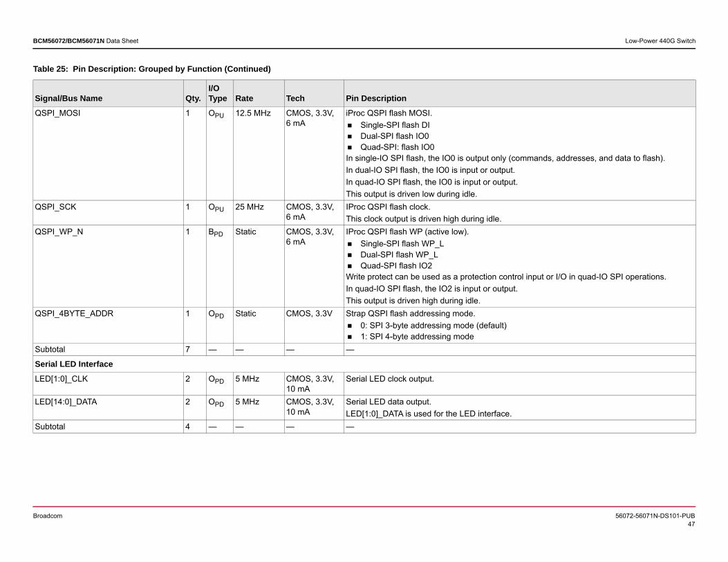
Broadcom 56072-56071N-DS101-PUB47
BCM56072/BCM56071N Data Sheet Low-Power 440G Switch
QSPI_MOSI 1 OPU 12.5 MHz CMOS, 3.3V, 6 mA
iProc QSPI flash MOSI. Single-SPI flash DI Dual-SPI flash IO0 Quad-SPI: flash IO0In single-IO SPI flash, the IO0 is output only (commands, addresses, and data to flash).In dual-IO SPI flash, the IO0 is input or output.In quad-IO SPI flash, the IO0 is input or output.This output is driven low during idle.
QSPI_SCK 1 OPU 25 MHz CMOS, 3.3V, 6 mA
IProc QSPI flash clock.This clock output is driven high during idle.
QSPI_WP_N 1 BPD Static CMOS, 3.3V, 6 mA
IProc QSPI flash WP (active low). Single-SPI flash WP_L Dual-SPI flash WP_L Quad-SPI flash IO2Write protect can be used as a protection control input or I/O in quad-IO SPI operations.In quad-IO SPI flash, the IO2 is input or output.This output is driven high during idle.
QSPI_4BYTE_ADDR 1 OPD Static CMOS, 3.3V Strap QSPI flash addressing mode. 0: SPI 3-byte addressing mode (default) 1: SPI 4-byte addressing mode
Subtotal 7 — — — —
Serial LED InterfaceLED[1:0]_CLK 2 OPD 5 MHz CMOS, 3.3V,
10 mASerial LED clock output.
LED[14:0]_DATA 2 OPD 5 MHz CMOS, 3.3V, 10 mA
Serial LED data output.LED[1:0]_DATA is used for the LED interface.
Subtotal 4 — — — —
Table 25: Pin Description: Grouped by Function (Continued)
Signal/Bus Name Qty.I/O Type Rate Tech Pin Description

Broadcom 56072-56071N-DS101-PUB48
BCM56072/BCM56071N Data Sheet Low-Power 440G Switch
Strap PinsIPROC_MHOST[1:0]_BOOT_DEV 2 IPD Static CMOS, 3.3V Strap MHOST boot device selection [1:0].
0: QSPI flash, starting at 0xF000_0000 (default) 1: Reserved 2: Reserved 3: Host processor (code is expected to be directly fetched and executed from external host
[eHost] memory)BOOT_DEV[2:0] 3 IPD Static CMOS, 3.3V Strap CPU ARM boot device selection [2:0].
0: QSPI flash, starting at 0xF000_0000 (default) 1: Parallel flash using NAND flash, starting at 0xE000_0000 2: Reserved 3: Host processor (code is expected to be directly fetched and executed from external host
[eHost] memory) 4: Reserved
I2C2_SA[1:0] 2 BOD Static CMOS, 3.3V Strap CMICx BSC.I2C2 address when in slave mode. 0: Address is 0x80 (default) 1: Address is 0x81 2: Address is 0x82 3: Address is 0x83
ALL_PLL_BYPASS 1 IPD Static CMOS, 3.3V Strap pin to bypass all PLLs. 0: Use PLL (default) 1: Bypass PLLSet 0 for normal operation.
BURN_IN 1 IPD Static CMOS, 3.3V Strap burn-in. 0: Normal mode (default) 1: Set for burn-inSet 0 for normal operation.
IPROC_DISABLE_MHOST0 1 IPD Static CMOS, 3.3V Strap iProc disable mHost0. 0: Enable (default) 1: Disable
Table 25: Pin Description: Grouped by Function (Continued)
Signal/Bus Name Qty.I/O Type Rate Tech Pin Description
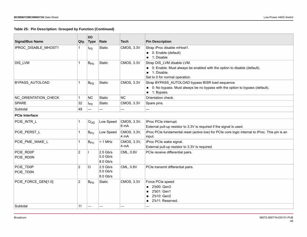
Broadcom 56072-56071N-DS101-PUB49
BCM56072/BCM56071N Data Sheet Low-Power 440G Switch
IPROC_DISABLE_MHOST1 1 IPD Static CMOS, 3.3V Strap iProc disable mHost1. 0: Enable (default) 1: Disable
DIS_LVM 1 BPD Static CMOS, 3.3V Strap DIS_LVM disable LVM. 0: Enable. Must always be enabled with the option to disable (default). 1: Disable.Set to 0 for normal operation.
BYPASS_AUTOLOAD 1 BPD Static CMOS, 3.3V Strap BYPASS_AUTOLOAD bypass BISR load sequence. 0: No bypass. Must always be no bypass with the option to bypass (default). 1: Bypass.
NC_ORIENTATION_CHECK 1 NC Static NC Orientation check.SPARE 32 IPD Static CMOS, 3.3V Spare pins.
Subtotal 49 — — — —
PCIe InterfacePCIE_INTR_L 1 OOD Low Speed CMOS, 3.3V,
6 mAIProc PCIe interrupt.External pull-up resistor to 3.3V is required if the signal is used.
PCIE_PERST_L 1 BPU Low Speed CMOS, 3.3V, 4 mA
iProc PCIe fundamental reset (active low) for PCIe core logic internal to iProc. This pin is an input.
PCIE_PME_WAKE_L 1 BPU < 1 MHz CMOS, 3.3V, 4 mA
IProc PCIe wake signal.External pull-up resistor to 3.3V is required.
PCIE_RD0PPCIE_RD0N
2 I 2.5 Gb/s 5.0 Gb/s8.0 Gb/s
CML, 0.8V PCIe receive differential pairs.
PCIE_TD0PPCIE_TD0N
2 O 2.5 Gb/s 5.0 Gb/s8.0 Gb/s
CML, 0.8V PCIe transmit differential pairs.
PCIE_FORCE_GEN[1:0] 2 BPD Static CMOS, 3.3V Force PCIe speed: 2'b00: Gen3 2'b01: Gen1 2'b10: Gen2 2'b11: Reserved.
Subtotal 11 — — — —
Table 25: Pin Description: Grouped by Function (Continued)
Signal/Bus Name Qty.I/O Type Rate Tech Pin Description

Broadcom 56072-56071N-DS101-PUB50
BCM56072/BCM56071N Data Sheet Low-Power 440G Switch
JTAG InterfaceJTCE[1:0] 2 IPD Static CMOS, 3.3V JTAG test enable [JTCE1, JTCE0].
00: Normal mode (default) 01: ARM debug mode 10: Reserved 11: JTAG modeNOTE: An external pull-down resistor must be added to ground for normal switch operation.
JTCK 1 IPD 12.5 MHz CMOS, 3.3V JTAG test clock.
JTDI 1 IPU 12.5 MHz CMOS, 3.3V JTAG test data input.
JTDO 1 OPU 12.5 MHz CMOS, 3.3V, 8 mA
JTAG test data output.
JTMS 1 IPU 12.5 MHz CMOS, 3.3V JTAG test mode select.
JTRST_L 1 IPU 12.5 MHz CMOS, 3.3V JTAG test controller reset.Must be pulled low during normal switch operation.
Subtotal 7 — — — —
Merlin (TSC4Q) Port SignalsTSCQ[2:0]_RD[3:0]pTSCQ[2:0]_RD[3:0]n
24 I 1.25 Gb/s to 10.9375 Gb/s
CML, 0.8V Merlin receiver differential pairs.
TSCQ[2:0]_TD[3:0]pTSCQ[2:0]_TD[3:0]n
24 O 1.25 Gb/s to 10.9375 Gb/s
CML, 0.8V Merlin transmitter differential pairs.
Subtotal 48 — — — —
Falcon (TSC4F) Port SignalsTSCF[3:0]_RD[3:0]pTSCF[3:0]_RD[3:0]n
32 I 1.25 Gb/s to 27.34375 Gb/s
CML, 0.8V Falcon receiver differential pairs.
TSCF[3:0]_TD[3:0]pTSCF[3:0]_TD[3:0]n
32 O 1.25 Gb/s to 27.34375 Gb/s
CML, 0.8V Falcon transmitter differential pairs.
Subtotal 64 — — — —
Table 25: Pin Description: Grouped by Function (Continued)
Signal/Bus Name Qty.I/O Type Rate Tech Pin Description

Broadcom 56072-56071N-DS101-PUB51
BCM56072/BCM56071N Data Sheet Low-Power 440G Switch
MIIM InterfaceMDC0 1 B 12.5 MHz VDDO_MDIO,
3.3V/1.2V, 14 mA
Serial management clock, used to communicate to external GPHY devices under software control.Clause 22 and 45 compliant.NOTE: Must be pulled up to the same power rail as VDDO_MDIO when set to 1.
MDC1 1 B 12.5 MHz VDDO_MDIO, 3.3V/1.2V, 14 mA
Serial management clock, used to communicate to external GPHY devices under software control.Clause 22 and 45 compliant.NOTE: Must be pulled up to the same power rail as VDDO_MDIO when set to 1.
MDC2 1 B 12.5 MHz VDDO_MDIO, 3.3V/1.2V, 14 mA
Serial management clock, used to communicate to external GPHY devices under software control.Clause 22 and 45 compliant.NOTE: Must be pulled up to the same power rail as VDDO_MDIO when set to 1.
MDIO0 1 B 12.5 MHz VDDO_MDIO, 3.3V/1.2V, 14 mA
Serial management data, used to communicate to external GPHY devices under software control.Clause 22 and 45 compliant.
MDIO1 1 B 12.5 MHz VDDO_MDIO, 3.3V/1.2V, 14 mA
Serial management data, used to communicate to external GPHY devices under software control.Clause 22 and 45 compliant.
MDIO2 1 B 12.5 MHz VDDO_MDIO, 3.3V/1.2V, 14 mA
Serial management data, used to communicate to external GPHY devices under software control.Clause 22 and 45 compliant.
Subtotal 6 — — — —
BSC InterfaceI2C0_SCL 1 BOD 100 kHz/
400 kHzCMOS, 3.3V iProc BSC (I2C).
BSC interface clocks. External pull-up resistor is required. Supports master mode only.I2C0_SDA 1 BOD 100 kHz/
400 kHzCMOS, 3.3V iProc BSC (I2C) – Master mode only.
BSC interface data. External pull-up resistor is required. Supports master mode only.I2C1_SCL 1 BOD 100 kHz/
400 kHzCMOS, 3.3V CMICx BSC (I2C).
BSC interface clocks. External pull-up resistor is required. Supports master mode and slave mode. Default power on at slave mode.
Table 25: Pin Description: Grouped by Function (Continued)
Signal/Bus Name Qty.I/O Type Rate Tech Pin Description

Broadcom 56072-56071N-DS101-PUB52
BCM56072/BCM56071N Data Sheet Low-Power 440G Switch
I2C1_SDA 1 BOD 100 kHz/400 kHz
CMOS, 3.3V CMICx BSC (I2C).BSC interface data. External pull-up resistor is required. Supports master mode and slave mode. Default power on at slave mode.
Subtotal 4 — — — —
BroadSync InterfaceBS[1:0]_CLK 2 BPD 2 MHz/
10 MHzCMOS, 3.3V, 6 mA
BroadSync bit clock.Used for the data transfer of the synchronized time code. When configured as outputs, the BS_HEARTBEAT and BS_TIME_CODE signals are driven off the rising edge of the BS_CLK.When configured as inputs, the BS_HEARTBEAT and BS_TIME_CODE signals are sampled off the negative edge of the BS_CLK.In IEEE 1588 default mode, BS0_CLK is defined as 10-MHz clock output.
BS[1:0]_HB 2 BPD 1 Hz (1 PPS)/4 kHz/2 MHz
CMOS, 3.3V, 6 mA
BroadSync heartbeat clock that signal the start of the transmission of the synchronized time code.This signal can be configured through CMIC register as an output or an input.When it is configured as an output, the BS_HEARTBEAT signal is driven off the rising edge of the BS_CLK.When it is configured as an input, the BS_HEARTBEAT signal is sampled off the negative edge of the BS_CLK.In IEEE 1588 default mode, BS0_HEARTBEAT is defined as 4 kHz clock output (typically connected to PHY's SYNC_IN pin).
BS[1:0]_TC 2 BPD 2 MHz CMOS, 3.3V, 6 mA
BroadSync synchronized time code.Serially shifts the time code, one bit per rising edge of the BS_CLK. This signal can be configured through CMIC register as an output or an input.When it is configured as an output, the BS_TIME_CODE signal is driven off the rising edge of the BS_CLK.When it is configured as an input, BS_TIME_CODE signal is sampled off the negative edge of the BS_CLK.
Table 25: Pin Description: Grouped by Function (Continued)
Signal/Bus Name Qty.I/O Type Rate Tech Pin Description

Broadcom 56072-56071N-DS101-PUB53
BCM56072/BCM56071N Data Sheet Low-Power 440G Switch
TS_GPIO[2:0] 3 B < 1 MHz CMOS, 3.3V, 6 mA
General-purpose I/O signals with the ability to trigger internal timestamp capture in input mode or be automatically controlled by the TimeSync logic in output mode. These signals can also be configured as general-purpose outputs or inputs (with interrupt generation capability). When configured as an input, a weak internal pull-up or pull-down resistor can be enabled. By default, these signals are configured as inputs with an internal pull-up resistor enabled. These signals return to the default state when the SYS_RST_N signal is asserted.
Subtotal 9 — — — —
Synchronous EthernetEXT_RCVRD_CLK[1:0] 2 IPD ≤
156.25 MHzCMOS, 3.3V Recovered clock inputs to DPLL function from external source.
EXT_RCVRD_CLK[1:0]_VLD 2 IPD Low Speed CMOS, 3.3V Recovered clock input to DPLL function valid indicators.
L1_RCVRD_CLK 1 O 25 MHz CMOS, 3.3V, 14 mA
Primary recovered clock.Recovered clock outputs from internal SerDes. Can be selected from any of the switch internal SerDes cores, LCPLL0_FREF or the EXT_RCVRD_CLK[1:0] pin. Recovered clock does not support 10M and 100M speeds. This clock is sent out to support L1 synchronization. Refer to the TOP_MISC_CONTROL_2 and TOP_L1_RCVD_CLK_CONTROL. registers.In IEEE 1588 default mode, this pin is defined as CDR clock 1 output.
L1_RCVRD_CLK_BKP 1 O 25 MHz CMOS, 3.3V, 14 mA
Secondary recovered clock.Backup recovered clock outputs from internal SerDes. Can be selected from any of the switch internal SerDes cores, LCPLL0_FREF or the EXT_RCVRD_CLK[1:0] pin. This clock is used when the primary recovered clock is not reliable. Refer to the TOP_MISC_CONTROL_2 and TOP_L1_RCVD_CLK_CONTROL registers.In IEEE 1588 default mode, this pin is defined as CDR clock 2 output.
L1_RCVRD_CLK_VLD 1 O Low Speed CMOS, 3.3V, 6 mA
Indicates the primary recovered clock has a valid link status needed for the recovered clock. When this signal is set to 1, L1_RCVRD_CLK is generated based on the recovered clock. This pin can be configured to output the inverse of L1_RCVRD_CLK signal.
L1_RCVRD_CLK_VLD_BKP 1 O Low Speed CMOS, 3.3V, 6 mA
Indicates the secondary recovered clock has a valid link status needed for the recovered clock. When this signal is set to 1, L1_RCVRD_CLK_BKUP is generated based on the recovered clock. This pin can be configured to output the inverse of L1_RCVRD_CLK signal.
Subtotal 8 — — — —
Table 25: Pin Description: Grouped by Function (Continued)
Signal/Bus Name Qty.I/O Type Rate Tech Pin Description

Broadcom 56072-56071N-DS101-PUB54
BCM56072/BCM56071N Data Sheet Low-Power 440G Switch
Miscellaneous SignalsAVS[2:0] 3 OPD Static CMOS, 3.3V,
6 mAAdaptive voltage scaling (AVS) is not supported. 3’b000: (default)
SYS_RST_L 1 IPU Low Speed CMOS, 3.3V Reset input for the entire chip (active low). This signal should be connected to the system’s power-on reset logic.
POR_OUT_L 1 OPU Low Speed CMOS, 3.3V, 6 mA
Power-on reset output (active low). This output is asserted on power-on-reset and is also controlled by the DMU_PCU_PCIE_SLAVE_RESET_MODE and DMU_PCU_POR_CONTROL registers based on the dmu_io_por_out_n assertions.
RESCAL[1:0]_REXT 2 B Static 0.8V External resistor. Connect to 4.53-kΩ ± 1% resistor to the respective RESCAL[2:0]_AVSS pins by placing the resistors under the BGA in the via field.
VDD_SENSE 1 O Static 1.0V Core voltage monitor.Used for remote sensing of VDDC rail. This pin connects directly to the die VDDC rail.This pin should be connected to the VRM positive sense pin. If not used, leave pin no connect.
VSS_SENSE 1 O Static 0V Ground monitor.Used for remote sensing of GND rail. This pin connects directly to the die GND rail.This pin should be connected to VRM negative sense pin. If not used, leave pin no connect.
Subtotal 9 — — — —
System Reference ClocksXTALPXTALN
2 I 50 MHz 1.8V Required crystal/oscillator differential input.The clock source can be an oscillator or a crystal as determined by the XTAL_BYPASS pin.The frequency of this input is determined by the state of the strap_xtal_freq_sel strap that is shared with the L1_RCVRD_CLK_VLD pin.By default, this clock input drives all the functions of the device for a solution without the following optional functions: XFI/HiGig, TimeSync, SyncE, and BroadSync applications. By default, timestamping functions are driven from this clock unless the TimeSync clock is used.
Table 25: Pin Description: Grouped by Function (Continued)
Signal/Bus Name Qty.I/O Type Rate Tech Pin Description

Broadcom 56072-56071N-DS101-PUB55
BCM56072/BCM56071N Data Sheet Low-Power 440G Switch
LCPLL0_FREFPLCPLL0_FREFN
2 I 50 MHz/156.25 MHz
CML, 1.8V LCPLL reference clock input.SerDes and 1588 reference clock. The default input reference clock required is 156.25 MHz.For designs that require a common clock source for TS_PLL, BSPLL[1:0] and LCPLL for minimal jitter, a 50-MHz OCXO differential input is required. The strap_lcpll1_refclk_sel strap pin should be set to 1 for this configuration.For designs that do not have such requirements, a 156.25-MHz differential clock input is required. In this configuration, the strap_lcpll1_refclk_sel strap pin should be set to 0.
PCIE_REFCLKPPCIE_REFCLKN
2 I 100 MHz CML, 0.8V PCIe SerDes reference clock. Requires a 100Ω external termination resistor.
TS_PLL_FREFPTS_PLL_FREFN
2 I 50 MHz CML, 1.8V Optional differential reference clock from the external crystal source.
BSPLL[1:0]_FREFPBSPLL[1:0]_FREFN
4 I 50 MHz CML, 1.8V Optional differential reference clock from the external crystal source.
Subtotal 28 — — — —
Factory Use Only (Test) SignalsAVS_VTMON_ADC 1 I — Analog,
VariableTest signal for factory use only. Do not connect to this signal.
AVS_VTMON_DAC 1 O — Analog, Variable
Test signal for factory use only. Do not connect to this signal.
CHIP_TEST_MODE_EN_RESERVED 1 IPD Static 3.3V Test mode enable.NOTE: For internal testing use only. Must add an external pull-down resistor to GND for normal operation.
CHIP_TEST_MODE[4:0]_RESERVED 5 IPD Static 3.3V Test mode selection.NOTE: For internal testing use only. Leave them floating for normal operation.
Subtotal 30 — — — —
Digital PowerVDDO_3P3 21 I PWR 3.3V Digital power.OTPC_VDD1P8 1 I PWR 1.8V OTPC power.VDDO_MDIO 1 I PWR 3.3V/1.2V MDIO power.VDDC (Programmable) 46 I PWR 0.88V Power for core logic (AVS).Subtotal 69 — — — —
Table 25: Pin Description: Grouped by Function (Continued)
Signal/Bus Name Qty.I/O Type Rate Tech Pin Description

Broadcom 56072-56071N-DS101-PUB56
BCM56072/BCM56071N Data Sheet Low-Power 440G Switch
Analog PowerBSPLL0_AVDD1P8 2 I PWR 1.8V BroadSync 0 PLL power.BSPLL1_AVDD1P8 2 I PWR 1.8V BroadSync 1 PLL power.GEN_PLL_VDD1P8 2 I PWR 1.8V 1.8V analog power for general PLL.CORE_PLL_VDD1P8 2 I PWR 1.8V 1.8V analog power for core PLL.LCPLL0_AVDD1P8 2 I PWR 1.8V LCPLL0 power.XTAL_AVDD1P8 1 I PWR 1.8V Power for XTALP/N PLL.TS_PLL_VDD1P8 2 I PWR 1.8V Time stamp PLL power.PCIE_PVDD_0P8 2 I PWR 0.8V PCIe PLL circuit power.PCIE_RTVDD_0P8 2 I PWR 0.8V PCIe transmitter/receiver circuit power.AVS_VTMON_VDDV1P8 1 I PWR 1.8V 1.8V analog power for VTMON block.TSCQ[2:0]_PVDD0P8 3 I PWR 0.8V Merlin PLL power.TSCQ_RTVD_0P8 12 I PWR 0.8V Merlin receiver/transmitter power.TSCF[3:0]_PVDD_0P8 4 I PWR 0.8V Falcon PLL power.TSCF_PVDD1P8 4 I PWR 1.8V Falcon PLL power.TSCF_RTVDD0P8 20 I PWR 0.8V Falcon receiver power.TSCF_TVDD1P2 4 I PWR 1.2V Falcon transmitter power.
These pins are normally connected to filtered 1.20V. 92.RESCAL[1:0]_AVDD0P8 2 I PWR 0.8V RESCAL circuit power.PGW_PLL_AVDD1P8 1 I PWR 1.8V PGW PLL power.AVDD_1P8 2 I PWR 1.8V Analog power supply.Subtotal 70 — — — —
GroundAGND 364 I GND N/A Analog ground.GND 73 I GND N/A Ground.Subtotal 437 — — — —
Table 25: Pin Description: Grouped by Function (Continued)
Signal/Bus Name Qty.I/O Type Rate Tech Pin Description

Broadcom 56072-56071N-DS101-PUB57
BCM56072/BCM56071N Data Sheet Low-Power 440G Switch
5.2 Pin ListThe pin list and ballout diagram for the BCM56072/BCM56071N are provided in a spreadsheet available on the Broadcom Customer Support Portal (docSAFE) collateral distribution site. The spreadsheet serves as the official document containing the device's signal mapping. Refer to the BCM56072 Ballout file (BCM56072_ballout_revxx).
5.3 Shared Strap PinsTable 26: Shared Strap Pins
Strap Pins Function Descriptionstrap_tscq0_pwr_off Indicates TSCQ0 power is off. Used to turn off the TSCQ0 active circuits if this
TSC is unused. This saves dynamic/static power.0: Indicates power is on (default).1: Indicates power is off.Shared with GPIO0.
strap_tscq1_pwr_off Indicates TSCQ1 power is off. Used to turn off the TSCQ1 active circuits if this TSC is unused. This saves dynamic/static power.0: Indicates power is on (default).1: Indicates power is off.Shared with GPIO1.
strap_tscq2_pwr_off Indicates TSCQ2 power is off. Used to turn off the TSCQ2 active circuits if this TSC is unused. This saves dynamic/static power.0: Indicates power is on (default).1: Indicates power is off.Shared with GPIO2.
strap_tscf0_pwr_off Indicates TSCF0 power is off. Used to turn off the TSCF0 active circuits if this TSC is unused. This saves dynamic/static power.0: Indicates power is on (default).1: Indicates power is off.Shared with GPIO8.
strap_tscf1_pwr_off Indicates TSCF1 power is off. Used to turn off the TSCF1 active circuits if this TSC is unused. This saves dynamic/static power.0: Indicates power is on (default).1: Indicates power is off.Shared with GPIO9.
strap_tscf2_pwr_off Indicates TSCF2 power is off. Used to turn off the TSCF2 active circuits if this TSC is unused. This saves dynamic/static power.0: Indicates power is on (default).1: Indicates power is off.Shared with GPIO10.
strap_tscf3_pwr_off Indicates TSCF3 power is off. Used to turn off the TSCF3 active circuits if this TSC is unused. This saves dynamic/static power.0: Indicates power is on (default).1: Indicates power is off.Shared with GPIO11.
strap_lcpll1_refclk_sel LCPLL0 reference clock source selection.0: From LCPLL0_FREFP/N differential pads (default).1: From XTAL P/N PLL.Pin shared with l1_rcvrd_clk_valid_bkup.
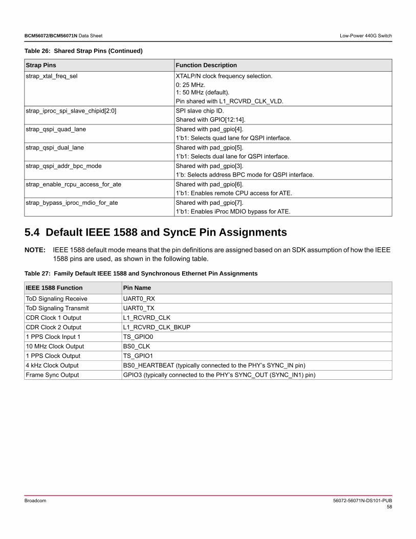
Broadcom 56072-56071N-DS101-PUB58
BCM56072/BCM56071N Data Sheet Low-Power 440G Switch
5.4 Default IEEE 1588 and SyncE Pin AssignmentsNOTE: IEEE 1588 default mode means that the pin definitions are assigned based on an SDK assumption of how the IEEE
1588 pins are used, as shown in the following table.
strap_xtal_freq_sel XTALP/N clock frequency selection.0: 25 MHz.1: 50 MHz (default).Pin shared with L1_RCVRD_CLK_VLD.
strap_iproc_spi_slave_chipid[2:0] SPI slave chip ID.Shared with GPIO[12:14].
strap_qspi_quad_lane Shared with pad_gpio[4].1’b1: Selects quad lane for QSPI interface.
strap_qspi_dual_lane Shared with pad_gpio[5].1’b1: Selects dual lane for QSPI interface.
strap_qspi_addr_bpc_mode Shared with pad_gpio[3].1’b: Selects address BPC mode for QSPI interface.
strap_enable_rcpu_access_for_ate Shared with pad_gpio[6].1’b1: Enables remote CPU access for ATE.
strap_bypass_iproc_mdio_for_ate Shared with pad_gpio[7].1’b1: Enables iProc MDIO bypass for ATE.
Table 27: Family Default IEEE 1588 and Synchronous Ethernet Pin Assignments
IEEE 1588 Function Pin NameToD Signaling Receive UART0_RXToD Signaling Transmit UART0_TXCDR Clock 1 Output L1_RCVRD_CLKCDR Clock 2 Output L1_RCVRD_CLK_BKUP1 PPS Clock Input 1 TS_GPIO010 MHz Clock Output BS0_CLK1 PPS Clock Output TS_GPIO14 kHz Clock Output BS0_HEARTBEAT (typically connected to the PHY’s SYNC_IN pin)Frame Sync Output GPIO3 (typically connected to the PHY’s SYNC_OUT (SYNC_IN1) pin)
Table 26: Shared Strap Pins (Continued)
Strap Pins Function Description
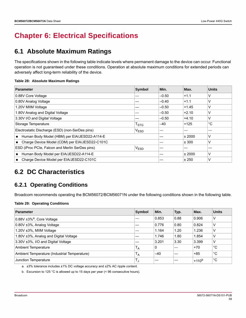
Broadcom 56072-56071N-DS101-PUB59
BCM56072/BCM56071N Data Sheet Low-Power 440G Switch
Chapter 6: Electrical Specifications
6.1 Absolute Maximum RatingsThe specifications shown in the following table indicate levels where permanent damage to the device can occur. Functional operation is not guaranteed under these conditions. Operation at absolute maximum conditions for extended periods can adversely affect long-term reliability of the device.
6.2 DC Characteristics
6.2.1 Operating ConditionsBroadcom recommends operating the BCM56072/BCM56071N under the following conditions shown in the following table.
Table 28: Absolute Maximum Ratings
Parameter Symbol Min. Max. Units0.88V Core Voltage — –0.50 +1.1 V0.80V Analog Voltage — –0.40 +1.1 V1.20V MIIM Voltage — –0.50 +1.45 V1.80V Analog and Digital Voltage — –0.50 +2.10 V3.30V I/O and Digital Voltage — –0.50 +4.10 VStorage Temperature TSTG –40 +125 °C
Electrostatic Discharge (ESD) (non-SerDes pins) VESD — — —
Human Body Model (HBM) per EIA/JESD22-A114-E — ± 2000 V Charge Device Model (CDM) per EIA/JESD22-C101C — ± 300 VESD (iProc PCIe, Falcon and Merlin SerDes pins) VESD — — —
Human Body Model per EIA/JESD22-A114-E — ± 2000 V Charge Device Model per EIA/JESD22-C101C — ± 250 V
Table 29: Operating Conditions
Parameter Symbol Min. Typ. Max. Units
0.88V ±3%a, Core Voltage
a. ±3% tolerance includes ±1% DC voltage accuracy and ±2% AC ripple content.
— 0.853 0.88 0.906 V
0.80V ±3%, Analog Voltage — 0.776 0.80 0.824 V1.20V ±3%, MIIM Voltage — 1.164 1.20 1.236 V1.80V ±3%, Analog and Digital Voltage — 1.746 1.80 1.854 V3.30V ±3%, I/O and Digital Voltage — 3.201 3.30 3.399 VAmbient Temperature TA 0 — +70 °C
Ambient Temperature (Industrial Temperature) TA –40 — +85 °C
Junction Temperature TJ — — +110b
b. Excursion to 125 °C is allowed up to 15 days per year (< 96 consecutive hours).
°C

Broadcom 56072-56071N-DS101-PUB60
BCM56072/BCM56071N Data Sheet Low-Power 440G Switch
6.2.2 Power-Up and Power-Down SpecificationsThe power-up and power-down requirements for the BCM56072/BCM56071N are outlined in the following figure. The sequence to power-up the voltage rails must be done in the order shown in the following figure. The power sequence is required, and the device does not support simultaneous power sequencing.
Figure 12: Power-Up and Power-Down Timing
6.2.2.1 Power-Up Sequence
The following table shows the power-up sequence.
Table 30: Power-Up Sequence
Sequence Power Power Supply Ramp Power Sequence Delay1 VDDO_3P3, VDDO_MDIO T1R <= 5 ms —
2 Core VDDC T2R <= 5 ms T1 = 25 ms
3 Analog core VDD0P8 T3R <= 3 ms T2 = 25 ms
4 All analog VDD1P8, including PVDD1P8 and OTP1P8
T4R <= 3 ms T3 = 25 ms
5 T VDD1P2 T5R <= 5 ms T4 = 25 ms
3.3V
1.8V
1.2V
0.88V
0.8V
VDDO_3P3, VDDO_MDIO
All Analog VDD1P8, include PVDD1P8/OTP1P8
Core
VDDC
Analog core VDD0P8
T VDD1P2
T1 T2 T3 T4
T3R
T4R
T5R
T2R
Power Sequence Delay
T2: 25 ms
T3: 25 ms
T4: 25 ms
Power Supply Ramp
T1R: <= 5 ms
T2R: <= 5 ms
T3R: <= 3 ms
T4R: <= 3 ms
T5R: <= 5 ms
T1: 25 ms
T1R

Broadcom 56072-56071N-DS101-PUB61
BCM56072/BCM56071N Data Sheet Low-Power 440G Switch
6.2.2.2 Power-Down Sequence
The following table shows the power-down sequence.
6.2.3 Sequencing Requirements for Non-Failsafe I/O SignalsThe following list of BCM56072/BCM56071N I/O pins are failsafe I/O: PCIE: PCIE_PERST_L, PCIE_PME_WAKE_L JTAG: JTMS, JTRST_L, JTDI, JTCK IPROC BROADSYNC: BS0_TC, BS1_HB, BS1_CLK, BS0_HB, BS1_TC, BS0_CLK IPROC_I2C: I2C1_SDA, I2C0_SCL, I2C1_SCL, I2C0_SDA IPROC_QSPI: QSPI_MISO, QSPI_MOSI, QSPI_WP_N, QSPI_HOLD_N IPROC_SPI: SPI_MOSI, SPI_MISO, SPI_SCK, SPI_SSN IPROC_TS_GPIO: TS_GPIO0, TS_GPIO1 IPROC_UART: UART1_SIN, UART0_CTS_N, UART0_SIN
NOTE: All I/O pins not included in the preceding list are non-failsafe.
There are two practical design configurations that allow the signals in the preceding list to meet the power sequencing requirements. The two configurations are as follows (and illustrated in the following figure): Connect the VDDA power supply for 3.3V of any other chip (driving the non-failsafe I/O to the BCM56072/BCM56071N
chip) to VDDB directly, which is the I/O power supply used by the BCM56072/BCM56071N device for the non-failsafe I/O.
Connect the VDDA power supply for 3.3V of any other chip (driving the non-failsafe I/O to the BCM56072/BCM56071N chip) to a different supply than the VDDB, which is the I/O power supply used by the BCM56072/BCM56071N device for the non-failsafe I/O. In this case, there is an additional power sequencing requirement (shown in the following figure and table).
Table 31: Power-Down Sequence
Sequence Power 1 T VDD1P22 All analog VDD1P8, including PVDD1P8 and OTP1P83 Analog core VDD0P84 Core VDDC5 VDDO_3P3, VDDO_MDIO

Broadcom 56072-56071N-DS101-PUB62
BCM56072/BCM56071N Data Sheet Low-Power 440G Switch
Figure 13: Non-Failsafe Sequence
Table 32: Non-Failsafe Power Sequencing Requirementsa, b
a. Valid operating conditions are listed in Table 29.
b. All power sequencing conditions must meet all conditions listed in Table 30.
Symbol RequirementstPU1 3.3V VDDB (VDDO3P3) Ramp-up start to 3.3V VDDA (IOVDDO) Ramp-up start time ≥ 0tPU2 3.3V VDDB (VDDO3P3) Valid to 3.3V VDDA (IOVDDO) Valid power-up time ≥ 0tPD1 3.3V VDDA (IOVDDO) Ramp-down start to 3.3V VDDB (VDDO3P3) Ramp-down start time ≥ 0tPD2 3.3V VDDA (IOVDDO) Ramp-down end to 3.3V VDDB (VDDO3P3) Ramp-down end time ≥ 0
IOVDDO
VDDA = 3.3V
# of I/O = N
OtherDevices
BCM56072
VDDB = 3.3V
MDIO SignalsNote: See signal list.
tPD2
tPD1tPU2
tPU1
3.3V IO_0
3.3V IO_N Fiber LOS Signal Inputs
VDDO3P3
VDDB
VDDA
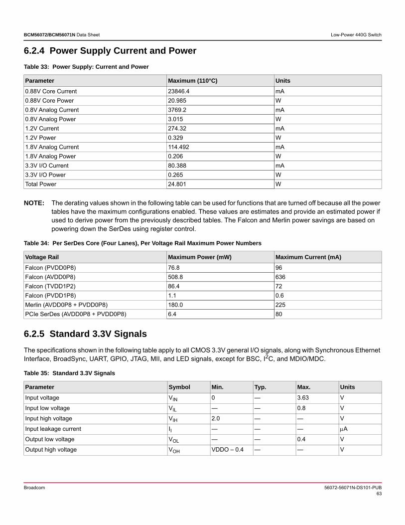
Broadcom 56072-56071N-DS101-PUB63
BCM56072/BCM56071N Data Sheet Low-Power 440G Switch
6.2.4 Power Supply Current and Power
NOTE: The derating values shown in the following table can be used for functions that are turned off because all the power tables have the maximum configurations enabled. These values are estimates and provide an estimated power if used to derive power from the previously described tables. The Falcon and Merlin power savings are based on powering down the SerDes using register control.
6.2.5 Standard 3.3V SignalsThe specifications shown in the following table apply to all CMOS 3.3V general I/O signals, along with Synchronous Ethernet Interface, BroadSync, UART, GPIO, JTAG, MII, and LED signals, except for BSC, I2C, and MDIO/MDC.
Table 33: Power Supply: Current and Power
Parameter Maximum (110°C) Units0.88V Core Current 23846.4 mA0.88V Core Power 20.985 W0.8V Analog Current 3769.2 mA0.8V Analog Power 3.015 W1.2V Current 274.32 mA1.2V Power 0.329 W1.8V Analog Current 114.492 mA1.8V Analog Power 0.206 W3.3V I/O Current 80.388 mA3.3V I/O Power 0.265 WTotal Power 24.801 W
Table 34: Per SerDes Core (Four Lanes), Per Voltage Rail Maximum Power Numbers
Voltage Rail Maximum Power (mW) Maximum Current (mA)Falcon (PVDD0P8) 76.8 96Falcon (AVDD0P8) 508.8 636Falcon (TVDD1P2) 86.4 72Falcon (PVDD1P8) 1.1 0.6Merlin (AVDD0P8 + PVDD0P8) 180.0 225PCIe SerDes (AVDD0P8 + PVDD0P8) 6.4 80
Table 35: Standard 3.3V Signals
Parameter Symbol Min. Typ. Max. UnitsInput voltage VIN 0 — 3.63 V
Input low voltage VIL — — 0.8 V
Input high voltage VIH 2.0 — — V
Input leakage current II — — — A
Output low voltage VOL — — 0.4 V
Output high voltage VOH VDDO – 0.4 — — V

Broadcom 56072-56071N-DS101-PUB64
BCM56072/BCM56071N Data Sheet Low-Power 440G Switch
6.2.6 PCIe Characteristics
6.2.7 I2C SignalsI2C[1:0]_SCL and I2C[1:0]_SDA are bidirectional open-drain signals. An external pull-up to 3.3V should be provided on the board. I2C[1:0]_SA1 and I2C[1:0]_SA0 are standard 3.3V signals.
Table 36: PCIe DC Characteristics
Parameter Symbol Min. Typ. Max. Units
TransmitterOutput impedance (differential) ROUT — 100 — Ω
Output voltage (differential pk-pk) VOD — — 1200 mVppd
ReceiverInput impedance (differential) RIN — 100 — ΩInput voltage (differential pk-pk) VID 175 — 2000 mVppd
Table 37: I2C Signals
Parameter Symbol Condition Min. Typ. Max. UnitsInput voltage VIN — 0 — 3.63 V
Input low voltage VIL — 0 — 0.3 × VDDO3P3 V
Input high voltage VIH — 0.7 × VDDO3P3 — — V
Input leakage current II — — — — A
Output low voltage VOL IOL = 8 mA — — 0.4 V
NOTE: I2C I/Os are true open-drain type and require external pull-up resistors. Overshoot: The maximum limit is: 500 mV above supply for no more than 10% of the duty cycle. Undershoot: The maximum limit is
500 mV below ground for no more than 10% of the duty cycle.

Broadcom 56072-56071N-DS101-PUB65
BCM56072/BCM56071N Data Sheet Low-Power 440G Switch
6.2.8 Reference ClocksThe following two figures apply to all reference clocks in this subsection.
Figure 14: Reference Clock Single-Ended DC Parameters
Figure 15: Reference Clock Differential DC Parameters
6.2.8.1 LCPLL0 Reference Clock (LCPLL0_FREF)
The required default clock is 156.25 MHz. LCPLL0 provides 156.25-MHz reference clocks to SerDes blocks.
Table 38: Core PLL Reference Clock DC Parameters
Parameter Symbol Min. Typ. Max. UnitsCommon mode voltage Vcm — 900 — mVse
a
a. mVse means mV single-ended.
Differential swing Vdiff 500 — 1800 mVppdb
b. mVppd means mV peak-to-peak differential.
Internal AC couplingc
c. External AC coupling is required. The recommended AC-coupling capacitor value is 10 nF.
Cac — — — pF
Internal differential termination Rterm — 100 — Ω
Vihse
Vcm
Vilse
Vdiff

Broadcom 56072-56071N-DS101-PUB66
BCM56072/BCM56071N Data Sheet Low-Power 440G Switch
6.2.8.2 TimeSync PLL Reference Clock (TS_PLL_FREF)
The TimeSync PLL clocks the TimeSync and timestamp logic distributed throughout the device.
6.2.8.3 PCIe PLL Reference Clock (PCIe_REFCLK)
The PCI Express PLL clock handles clocking for the SerDes used for PCI Express connectivity and has the input structure shown in the following figure.
Figure 16: PCI Express PLL Input Structure
Table 39: TimeSync PLL Reference Clock DC Parameters
Parameter Symbol Min. Typ. Max. UnitsCommon mode voltage Vcm — 900 — mVse
Differential swing Vdiff 500 — 1800 mVppd
Internal AC couplinga
a. External AC coupling is required. The recommended AC-coupling capacitor value is 10 nF.
Cac — — — pF
Internal differential termination Rterm — 100 — Ω
Table 40: PCI Express PLL Reference Clock DC Parameters
Parameter Symbol Min. Typ. Max. UnitsCommon mode voltage Vcm — 900 — mVse
Single ended swing Vilse or Vihse 0 — 800 mVse
Differential swing Vdiff 600 — 1200 mVppd
Internal AC coupling Cac — 6 — pF
Internal differential termination Rterm — — — Ω
NOTE: External AC coupling is required. Recommended AC-coupling capacitor value is 10 nF. External 100Ω termination resistor is required.
PLL
PVDD0p8
Cac
REFCLK_P
REFCLK_N
Cac

Broadcom 56072-56071N-DS101-PUB67
BCM56072/BCM56071N Data Sheet Low-Power 440G Switch
6.2.8.4 BroadSync PLL Reference Clocks (BS_PLL0_REFCLK and BS_PLL1_REFCLK)
The BroadSync PLLs clock the associated BroadSync block used to transmit or receive timing information from an external entity. They have the input structure shown in the following figure.
Figure 17: BroadSync PLL Input Structure
6.2.9 Merlin Transceiver Electrical Specifications
Table 41: BroadSync PLL Reference Clock DC Parameters
Parameter Symbol Min. Typ. Max. UnitsCommon mode voltage Vcm — 900 — mVse
Differential swing Vdiff 500 — 2000 mVppd
Internal AC couplinga
a. External AC coupling is required. The recommended AC-coupling capacitor value is 10 nF.
Cac — — — pF
Internal differential termination Rterm — 100 — Ω
Table 42: Merlin Transceiver Electrical Specifications
Parameter Symbol Min. Typ. Max. Units
ReceiverInput voltage (differential pk-pk), AC-coupled VID 85 — 1200 mVppd
Input impedance (differential), integrated on-chip RIN 80 100 120 Ω
Transmitter Output impedance (differential) ROUT 80 100 120 Ω
Transmitter (XFI) driver supply = 0.8VOutput voltage (differential pk-pk), programmable VOD 360 500 770 mVppd
Transmitter (SFI) driver supply = 0.8VOutput voltage (differential pk-pk), programmable VOD 500 600 700 mVppd
Transmitter (KR) driver supply = 0.8VOutput voltage (differential pk-pk), programmable VOD 800 900 1200 mVppd
PVDD1P8
REFCLK_P
REFCLK_N
RtermVcm

Broadcom 56072-56071N-DS101-PUB68
BCM56072/BCM56071N Data Sheet Low-Power 440G Switch
6.2.10 Falcon Quad SerDes Signal
6.2.11 AC-JTAGThe serial interface AC-JTAG for Falcon characteristics are shown in the following table.
The following two tables show the Falcon AC-JTAG settings and the corresponding typical voltages.
Table 43: Falcon Quad SerDes DC Characteristics
Parameter Symbol Min. Typ. Max. Units
ReceiverInput voltage (differential peak-to-peak), AC-coupled VID 85 — 1600 mVp-p
Input impedance (differential), integrated on-chip RIN 80 100 120 Ω
TransmitterOutput voltage (differential peak-to-peak), programmable VODpp 0 1000 1050 mVp-p
Output impedance (differential) ROUT 70 85 110 Ω
Table 44: Serial Interface AC-JTAG Characteristics
Parameter Symbol Description Min. Typ. Max. UnitsFault resistance detect Rsc Short circuit 0 — 5 Ω
Roc Open circuit 20 — — kΩ
Transmit voltage levels VTX Differential p-p 0.68 1.0 1.1 V
Transmit data rate — EXTEST_TRAIN 1 — 30 Mb/sOutput resistance RDRV DP or DM to VDD — 50 — Ω
Supply current IDD Operating mode — 56 — mA
Receiver input capacitance CIN DP or DM to GND — 0.5 0.6 pF
Common-mode voltage VCM — — VDD – 0.25 V
Comparator hysteresis VHYS Peak-to-peak 0 100 300 mV
Supply current IDD Operating mode — 500 — µA
Receive data rate — EXTEST_TRAIN 1 — 30 Mb/s
Table 45: AC-JTAG Transmit Setting (Driver Bias Current)
Cfg. Value Transmit Amplitude (Vpp) Cfg. Value TX Amplitude (Vpp)0111 0.34 1111 0.450110 0.35 1110 0.470101 0.36 1101 0.480100 0.38 1100 0.500011 0.40 1011 0.520010 0.41 1010 0.530001 0.43 1001 0.540000 0.44 1000 0.55

Broadcom 56072-56071N-DS101-PUB69
BCM56072/BCM56071N Data Sheet Low-Power 440G Switch
6.2.12 MIIM (MDIO) Signals
Table 46: AC-JTAG Receive Configuration
Cfg. Value RX Hysteresis (mVpp) Cfg. Value RX Hysteresis (mVpp)111 65 011 0110 58 010 90101 35 001 80100 20 000 75
Table 47: MIIM (Clause 45 Electrical Characteristics)
Parameter Symbol Condition Min. Typ. Max. UnitsInput voltage VIN — — 1.2 V
Input low voltage VIL — — – 0.35 × VDDO V
Input high voltage VIH — 0.65 × VDDO – – V
Input leakage current II — — – – A
Output low voltage VOL — — 0.4 – V
Output high voltage VOH — — VDDO – 0.4 – V
Table 48: MIIM (Clause 22 Electrical Characteristics)
Parameter Symbol Condition Min. Typ. Max. UnitsInput voltage VIN — 3.3 — V
Input low voltage VIL — — — 0.8 V
Input high voltage VIH — 2.0 — — V
Input leakage current II — — — — μA
Output low voltage VOL — — 0.4 — V
Output high voltage VOH — — VDDO – 0.4 — V
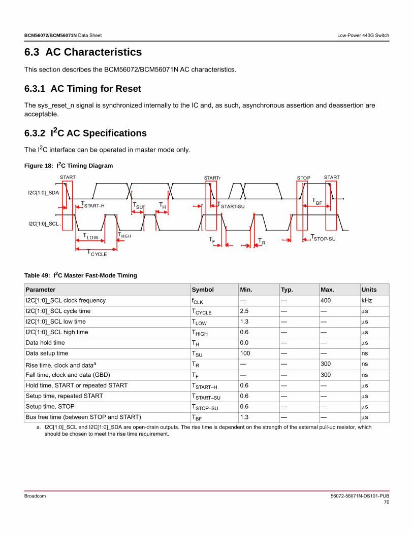
Broadcom 56072-56071N-DS101-PUB70
BCM56072/BCM56071N Data Sheet Low-Power 440G Switch
6.3 AC CharacteristicsThis section describes the BCM56072/BCM56071N AC characteristics.
6.3.1 AC Timing for ResetThe sys_reset_n signal is synchronized internally to the IC and, as such, asynchronous assertion and deassertion are acceptable.
6.3.2 I2C AC SpecificationsThe I2C interface can be operated in master mode only.
Figure 18: I2C Timing Diagram
Table 49: I2C Master Fast-Mode Timing
Parameter Symbol Min. Typ. Max. UnitsI2C[1:0]_SCL clock frequency fCLK — — 400 kHz
I2C[1:0]_SCL cycle time TCYCLE 2.5 — — s
I2C[1:0]_SCL low time TLOW 1.3 — — s
I2C[1:0]_SCL high time THIGH 0.6 — — s
Data hold time TH 0.0 — — s
Data setup time TSU 100 — — ns
Rise time, clock and dataa
a. I2C[1:0]_SCL and I2C[1:0]_SDA are open-drain outputs. The rise time is dependent on the strength of the external pull-up resistor, which should be chosen to meet the rise time requirement.
TR — — 300 ns
Fall time, clock and data (GBD) TF — — 300 ns
Hold time, START or repeated START TSTART–H 0.6 — — s
Setup time, repeated START TSTART–SU 0.6 — — s
Setup time, STOP TSTOP–SU 0.6 — — s
Bus free time (between STOP and START) TBF 1.3 — — s
TLOW
TSTART-H
TR
THIGH TSTOP-SU
TBF
IP_BSC_SCL
TCYCLE
THTSU
TF
START STARTr
TSTART-SU
STOP START
IP_BSC_SDAI2C[1:0]_SDA
I2C[1:0]_SCL

Broadcom 56072-56071N-DS101-PUB71
BCM56072/BCM56071N Data Sheet Low-Power 440G Switch
The BCM56072/BCM56071N device drives the I2C[1:0]_SCL clock, with a programmable speed of 100 kHz or 400 kHz based on the mode bit. The BCM56072/BCM56071N drives I2C[1:0]_SDA during a write operation and samples I2C[1:0]_SDA during a read operation.
Table 50: I2C Master Standard-Mode Timing
Parameter Symbol Min. Typ. Max. UnitsI2C[1:0]_SCL clock frequency fCLK — — 100 kHz
I2C[1:0]_SCL cycle time TCYCLE 10 — — s
I2C[1:0]_SCL low time TLOW 4.7 — — s
I2C[1:0]_SCL high time THIGH 4.0 — — s
Data hold time TH 0.0 — — s
Data setup time TSU 250 — — ns
Rise time, clock and dataa
a. I2C[1:0]_SCL and I2C[1:0]_SDA are open-drain outputs. The rise time is dependent on the strength of the external pull-up resistor, which should be chosen to meet the rise time requirement.
TR — — 1000 ns
Fall time, clock and data (GBD) TF — — 300 ns
Hold time, START or repeated START TSTART–H 4.0 — — s
Setup time, repeated START TSTART–SU 4.7 — — s
Setup time, STOP TSTOP–SU 4.0 — — s
Bus free time (between STOP and START) TBF 4.7 — — s

Broadcom 56072-56071N-DS101-PUB72
BCM56072/BCM56071N Data Sheet Low-Power 440G Switch
6.3.3 MIIM (MDIO) AC SpecificationsFigure 19: MIIM Interface Timing Diagram
Table 51: MDC/MDIO Timinga, b
a. Output load conditions = 25 pF.
b. External device to conform to IEEE specifications.
Parameter Symbol Min. Typ. Max. UnitsMDC clock frequency fCLK — 2.5 12.5 MHz
MDC cycle time TCYCLE 80 400 — ns
MDC duty cycle — 40 — 60 %MDIO setup time TSU 50 — — ns
MDIO hold time TH 0 — — ns
MDIO output delayc
c. MDIO output delay is programmable.
TOD 10 — 60 ns
TOD
50%
MDC
MDIO
TCYCLE TF
TR
TSU TH
VALID WRITE DATA VALID READ DATA

Broadcom 56072-56071N-DS101-PUB73
BCM56072/BCM56071N Data Sheet Low-Power 440G Switch
6.3.4 JTAG AC SpecificationsFigure 20: JTAG Timing
Table 52: AC Characteristics for JTAGa
a. Unless otherwise noted, the specifications are valid across the following operating conditions:
• The threshold value is at 50% of the applicable I/O rail voltage.• The default loading on an output is 5 pF.
Parameter Symbol Min. Typ. Max. UnitsJTAG_TCLK clock frequency fCLK — — 12.5 MHz
JTAG_TCLK duty cycle — 45 — 55 %JTAG_TCLK cycle time tCYCLE 80.0 — — ns
JTAG_TCLK falling edge to output valid.Applicable to JTAG_TDO.
tOD 0 — 25 ns
Data input setup time before JTAG_TCLK.Applicable to JTAG_TDI and JTAG_TMS.
tSU_JT 15 — — ns
Data hold time after JTAG_TCLK riseApplicable to JTAG_TDI and JTAG_TMS.
tH_JT 5 — — ns
Input setup time before JTAG_TCLK rising edge.Applicable to JTAG_TRST_N.
tSU_JTRS 15 — — ns
Input hold time after JTAG_TCLK rising edge.Applicable to JTAG_TRST_N.
tH_JTRS 5 — — ns
50%TCLKTCYCLE
TDI/TMS/TRST
TSU TH
TDO
TOD
VALID
VALID

Broadcom 56072-56071N-DS101-PUB74
BCM56072/BCM56071N Data Sheet Low-Power 440G Switch
6.3.5 BroadSync AC SpecificationsThe following two tables show the parameters for BroadSync timing, and the following two figures show the timing diagrams. See Section 6.3.16, BS0_CLK Output Clock, for the 10-MHz output clock specifications.
Figure 21: BroadSync Input Timing – Master Mode
Figure 22: BroadSync Output Timing – Slave Mode
Table 53: BroadSync Input Timing – Master Mode
Parameters Symbol Min. Typ. Max. UnitsBS*_BIT_CLK cycle time tCYC 100 — — ns
BS*_BIT_CLK duty cycle tHIGH 40 — 60 ns
BS*_TIME_VAL; BS*_SYNC input setup time tISU 30 — — ns
BS*_TIME_VAL; BS*_SYNC input hold time tIH 0 — — ns
Table 54: BroadSync Output Timing – Slave Mode
Parameters Symbol Min. Typ. Max. UnitsBS*_BIT_CLK cycle time tCYC 100 — — ns
BS*_BIT_CLK duty cycle tHIGH 40 — 60 ns
BS*_SYNC output delay tODS 0 — 25 ns
BS*_TIME_VAL output delay tODV 0 — 25 ns
50%BS_BIT_CLK
TCYCLE
BS_TIME_VALBS_SYNC
TISU
VALID INPUT
TIH
50%BS*_BIT_CLK
TCYCLE
BS*_SYNC
TODS
VALID OUTPUT
BS*_TIME_VAL
TODV
VALID OUTPUT

Broadcom 56072-56071N-DS101-PUB75
BCM56072/BCM56071N Data Sheet Low-Power 440G Switch
6.3.6 Synchronous Ethernet Interface Specifications
Figure 23: Synchronous Ethernet Output Timing Diagram
Figure 24: Synchronous Ethernet Interface Timing Diagram
Table 55: RCVRD_CLK[1:0]_OUT Output Timing
Parameter Symbol Min. Typ. Max. UnitsRCVRD_CLK[1:0]_OUT cycle time TCYCLE 6.4 — 40 ns
RCVRD_CLK[1:0]_OUT duty cycle THIGH 40 — 60 %
RCVRD_CLK[1:0]_OUT jitter RMS max. (12 kHz to 20 MHz) — — — 30 psRCVRD_CLK[1:0]_OUT rise time from 20% to 80% TOR — — 2.0 ns
RCVRD_CLK[1:0]_OUT fall time from 20% to 80% TOF — — 2.0 ns
Table 56: RCVRD_CLK[1:0]_VALID_OUT and RCVRD_CLK[1:0]_OUT Output Timing
Parameter Symbol Min. Typ. Max. UnitsRCVRD_CLK0_VALID_OUT to RCVRD_CLK0_OUT on time TCLK_ON0 0.35 — 5.0 ns
RCVRD_CLK0_VALID_OUT to RCVRD_CLK0_OUT off time TCLK_OFF0 0.35 — 2.0 ns
RCVRD_CLK1_VALID_OUT to RCVRD_CLK1_OUT on time TCLK_ON1 0.35 — 5.0 ns
RCVRD_CLK1_VALID_OUT to RCVRD_CLK1_OUT off time TCLK_OFF1 0.35 — 2.0 ns
TCYCLE
RCVRD_CLK[1:0]_OUT 50%20%20%
80% 80%
TOF TOR

Broadcom 56072-56071N-DS101-PUB76
BCM56072/BCM56071N Data Sheet Low-Power 440G Switch
6.3.7 iProc QSPI Interface Timing SpecificationsThe QSPI interface operates as a Master, allowing access to an external SPI Flash from which the microcontroller boot code can be loaded. The IP_QSPI_SCK, IP_QSPI_CS_N, and IP_QSPI_MOSI signals are outputs, while IP_QSPI_MISO is an input.
Figure 25: QSPI BSPI Mode Master Interface Timing
NOTE: The preceding BSPI node shows single-lane operation. IP_QSPI_WP_N and IP_QSPI_HOLD_N signals are used to support dual-lane and quad-lane operation.
Table 57: QSPI BSPI Mode Master Interface Timing Specifications
Parameters Symbol Conditions Min. Typ. Max. Units
QSPI clock frequencya
a. QSPI BSPI mode is used for initial code download when IP_BOOT_DEV = 2'b00 and read operations during runtime. The frequency is set to a reset default value of 25 MHz through CRU_CONTROL.QSPI_CLK_SEL. When register access is established, the same register can be written to change the QSPI interface frequency to a value of 25 MHz, 31.25 MHz, 50 MHz, or 62.5 MHz.
FCLK — 25 25 62.5 MHz
QSPI clock cycle time TCK — — 1/FCLK — ns
IP_QSPI_SCK clock high time TWH — 0.4TCK — 0.6TCK ns
IP_QSPI_SCK clock low time TWL — 0.4TCK — 0.6TCK ns
Chip Select (IP_QSPI_CS_N) output setup time TCES — 16.0 — — ns
Data Out (IP_QSPI_MOSI) valid time TVal — –3.0 — 4.0 ns
Data In (IP_QSPI_MISO) setup time TDS — 9.0 — — ns
Data In (IP_QSPI_MISO) hold time TDH — 1.0 — — ns
Rise Timeb
b. This parameter only applies to the output signals.
TR 20% to 80% — — 1.5 ns
Fall Timeb TF 20% to 80% — — 1.5 ns
QSPI_SCK
TVAL
TDS
VALID INPUT
TDH
VALID OUTPUT
TWH TWL
QSPI_MOSI
QSPI_MISO
50%
QIP_
IP_
IP_
IP_
SPI_CS_ N
TCES

Broadcom 56072-56071N-DS101-PUB77
BCM56072/BCM56071N Data Sheet Low-Power 440G Switch
Figure 26: QSPI MSPI Mode Master Interface Timing
Table 58: QSPI MSPI Mode Master Interface Timing Specifications
Parameters Symbol Conditions Min. Typ. Max. Units
QSPI clock frequencya
a. QSPI MSPI mode is typically used during runtime whenever write or erase operations are required.
FCLK — — 12.5 12.5 MHz
QSPI clock cycle time TCK — — 1/FCLK — ns
IP_QSPI_SCK clock high time TWH — 0.4TCK — 0.6TCK ns
IP_QSPI_SCK clock low time TWL — 0.4TCK — 0.6TCK ns
Chip Select (IP_QSPI_CS_N) output setup time TCSS — 12.0 — — ns
Chip Select (IP_QSPI_CS_N) output hold time TCSH — 1.0 — — ns
Data Out (IP_QSPI_MOSI) valid time TVal — 0 — 16.0 ns
Data In (IP_QSPI_MISO) setup time TDS — 12.0 — — ns
Data In (IP_QSPI_MISO) hold time TDH — 1.0 — — ns
Rise timeb
b. This parameter only applies to the output signals.
TR 20% to 80% — — 1.5 ns
Fall timeb TF 20% to 80% — — 1.5 ns
TCSS
50%
SFLASH_CLK
SFLASH_CS_L
SFLASH_IO1 (MISO)
Valid Output SFLASH_IO0
(MOSI)
TWH TWL TCSH
TCS
TVal
TDS TDH
50%
50% High-Z High-Z
Valid Input
50%

Broadcom 56072-56071N-DS101-PUB78
BCM56072/BCM56071N Data Sheet Low-Power 440G Switch
6.3.8 SPI Interface Timing Specification The SPI interface can be operated in two modes: master mode and slave mode.
Figure 27: SPI Interface Master Mode Timing Diagram
Table 59: SPI Master Mode Timing
Parameter Symbol Min. Typ. Max. UnitsSPI_SCK clock frequency fCLK — — 15.625 MHz
SPI_SCK cycle time TCYCLE 64 — — ns
SPI_SS_N output setup time t_css 10 TCYCLE/2 — ns
SPI_SS_N output hold time t_csh 20 — — nsSPI_MOSI valid time t_valid 10 — 20 nsSPI_MISO setup time t_setup 9 — — nsSPI_MISO hold time t_hold 12 — — ns

Broadcom 56072-56071N-DS101-PUB79
BCM56072/BCM56071N Data Sheet Low-Power 440G Switch
Figure 28: SPI Interface Slave Mode Timing Diagram
Table 60: SPI Slave Fast Mode Timing
Parameter Symbol Min. Typ. Max. UnitsSPI_SCK clock frequency fCLK — — 31.25 MHz
SPI_SCK cycle time TCYCLE 32 — — ns
SPI_SS_N setup time t1_setup 7 — — nsSPI_MOSI setup time t2_setup 7 — — nsSPI_MOSI hold time t_hold 0.5 — — nsSPI_MISO valid time t_valid 5 — 11 ns

Broadcom 56072-56071N-DS101-PUB80
BCM56072/BCM56071N Data Sheet Low-Power 440G Switch
6.3.9 iProc PCIe Interface Timing Specifications
6.3.9.1 PCIE_REFCLK Timing
Figure 29: PCIE_REFCLK Timing
Table 61: PCIe PLL Reference Clock AC Parameters
Parameter Symbol Min. Typ. Max. UnitsFrequency (1 / Tcycle) — — 100 — MHzTolerance — –300 — 300 PPMDuty cycle Tl / Th 40 50 60 %
Rise/fall time (20% to 80%) Tr / Tf — — 0.9 ns
RMS Jitter (10 kHz to 1.5 MHz) (Gen3 – 8 Gb/s) Tj — — 1.0 ps
RMS Jitter (10 kHz to 1.5 MHz) (Gen2 – 5 Gb/s) Tj — — 3.0 ps
RMS jitter (cycle-to-cycle) (Gen1 – 2.5 Gb/s) Tj — — 150 ps
TCYCLE
TF TR
TJ
PCIE_REFCLK

Broadcom 56072-56071N-DS101-PUB81
BCM56072/BCM56071N Data Sheet Low-Power 440G Switch
6.3.9.2 PCIe_RX Timing
Figure 30: PCIe_RX Timing Diagram
6.3.9.3 PCIe_TX Timing
Figure 31: PCIe_TX Timing Diagram
Table 62: PCIe_RX
Parameters Symbol Min. Typ. Max. UnitsBaud rate FREQ — 2.5, 5.0, or 8.0 — GbaudMinimum RX total jitter TJ 0.6 — — UI
NOTE: Includes on-chip AC-coupling capacitors.
Table 63: PCIe_Transmitter Output Timing
Parameters Symbol Condition Min. Typ. Max. UnitsBaud rate FREQ — — 2.5, 5.0, or 8.0 — GbaudOutput rise/fall time (20% to 80%) TR/TF — 30 — 90 ps
Output deemphasisa
a. The output deemphasis values listed in this table are the default settings. TX deemphasis can be software configured in the range of 0 db to 8 dB, overriding the defaults.
VOEQ Gen1 2.5 Gb/sGen1 5.0 Gb/s
–3.0–5.5
–3.5–6.0
–4.0–6.5
dB
Minimum TX total jitter TJ — 0.75 — — UI
PCIE_RXP/N
TR TF
PCIE_TXP/N

Broadcom 56072-56071N-DS101-PUB82
BCM56072/BCM56071N Data Sheet Low-Power 440G Switch
6.3.10 LED Controller Interface SpecificationsLED_CLK and LED_DATA are outputs. LED_CLK output clock period is 200 ns (5.0 MHz).
Figure 32: LED Timing Diagram
Table 64: LED Timinga
a. Timing figures are specified at the 50% crossing thresholds.
Parameter Symbol Min. Typ. Max. UnitsLED_CLK clock frequency fCLK — 5 5 MHz
LED_CLK cycle time TCYCLE — 200 200 ns
LED_CLK high time THIGH 70 100 130 ns
LED_CLK low time TLOW 70 100 130 ns
LED_DATA output hold time TOH 50 90 — ns
LED_DATA output setup time TOSU 50 90 — ns
50%LED_CLK
TCYCLE
LED_DATA
THIGH TLOW
TO SU
VALID OUTPUT
TOH

Broadcom 56072-56071N-DS101-PUB83
BCM56072/BCM56071N Data Sheet Low-Power 440G Switch
6.3.11 LCPLL0_FREF Clock RequirementsThe LCPLL0 takes a differential reference clock input from external crystal source. The default clock required is 156.25 MHz. LCPLL0 provides 156.25-MHz reference clocks to SerDes blocks.
If the use case requires the same clock source for TS_PLL/BSPLL/LCPLL0 inputs for minimal input jitter, such as for Synchronous Ethernet applications, the clock source for this PLL is a 50-MHz XTAL/OSC clock source. The characteristics of the reference clock input when the reference clock is 156.25 MHz is shown in the following figure.
Figure 33: LCPLL0_FREF Input Timing Diagram
Table 65: LCPLL0_FREF Input Requirementsa, b
a. AC-coupled externally.b. Internal 100Ω termination.
Requirement Symbol Min. Typ. Max. UnitsLCPLL0_FREF frequency — — 156.25 — MHzLCPLL0_FREF accuracy — –50 — +50 ppmLCPLL0_FREF duty cycle — 40 — 60 %Input voltage range VIN 500 — 2000 mVpp diff
Minimum input voltage VIN 0 — — VDC
Maximum input voltage VIN — — 1.0 VDC
LCPLL0_FREF Rise/Fall Time (10% to 90%) TR, TF — — 0.8 ns/Vpp diff
LCPLL0_FREF (156.25 MHz) jitter RMS max. (12 kHz to 20 MHz) — — — 0.3 ps
TCYCLE
50%
LCPLL0_FREF TF
TR
THIGH TLOW

Broadcom 56072-56071N-DS101-PUB84
BCM56072/BCM56071N Data Sheet Low-Power 440G Switch
The characteristics of the reference clock input when the reference clock is 50 MHz is shown in the following figure.
Figure 34: LCPLL0_FREF AC Timing
Table 66: LCPLL0_FREF AC Timing
Requirement Symbol Min. Typ. Max. UnitsCycle Time (50 MHz) TCYC — 20 — ns
Frequency — — 50 — MHzFrequency accuracy — –50 — +50 PPMDuty cycle TLOW/THIGH 40 50 60 %
Rise/fall time (20%, 80%) TR/TF — — 1 ns
RMS jitter (integrated from 12 kHz to 12.5 MHz) TJ — — 0.5 ps
Input voltage range VIN 500 — 1800 V
Minimum input voltage VIL 0 — — V
Maximum input voltage VIH — — 1.8 V
NOTE: Requires external AC coupling. Contains internal termination.
THIGH TLOW
TCYC
TFTR TJ
LCPLL0_FREFP/N

Broadcom 56072-56071N-DS101-PUB85
BCM56072/BCM56071N Data Sheet Low-Power 440G Switch
6.3.12 BSPLL0_FREF Clock RequirementsThe BroadSync 0 clock (BSPLL0_FREFP/N) requires a 50-MHz differential source with characteristics shown in the following figure. This reference clock input is optional.
Figure 35: BSPLL0_FREFP/N Input Timing Diagram
Table 67: BSPLL0_FREF Input Requirementsa, b
a. AC-coupled externally.b. Internal 100Ω termination.
Requirement Symbol Min. Typ. Max. UnitsBSPLL0_FREF frequency — — 50 — MHzBSPLL0_FREF accuracy — –50 — +50c
c. The ±50 ppm accuracy is the minimum requirement for the operation of Transparent Clock (TC) functionality only. Input clock accuracy may be application dependent.
ppm
BSPLL0_FREF duty cycle — 40 — 60 %Input voltage range VIN 500 — 1800 mVpp diffMinimum input voltage VIN 0.5 — — VDC
Maximum input voltage VIN — — 1.8 VDC
BSPLL0_FREF rise/fall time (10% to 90%) TR, TF — — 1.0 ns/Vpp diff
BSPLL0_FREF 50 MHz RMS jitter (integrated from 12 kHz to 20 MHz)
TJ — — 10 ps
TCYCLE
50%
BSPLL0_FREF TF
TR
THIGH TLOW

Broadcom 56072-56071N-DS101-PUB86
BCM56072/BCM56071N Data Sheet Low-Power 440G Switch
6.3.13 BSPLL1_FREF Clock Requirements The BroadSync 1 clock (BSPLL1_FREFP/N) requires a 50-MHz differential source with characteristics shown in the following figure. This reference clock input is optional.
Figure 36: BSPLL1_FREFP/N Input Timing Diagram
Table 68: BSPLL1_FREF Input Requirementsa, b
a. AC-coupled externally.b. Internal 100Ω termination.
Requirement Symbol Min. Typ. Max. UnitsBSPLL1_FREF frequency — — 50 — MHzBSPLL1_FREF accuracy — –50 — +50c
c. The ±50 ppm accuracy is the minimum requirement for the operation of Transparent Clock (TC) functionality only. Input clock accuracy may be application dependent.
ppm
BSPLL1_FREF duty cycle — 40 — 60 %Input voltage range VIN 500 — 1800 mVpp diffMinimum input voltage VIN 0.5 — — VDC
Maximum input voltage VIN — — 1.8 VDC
BSPLL1_FREF rise/fall time (10% to 90%) TR, TF — — 1.0 ns/Vpp diff
BSPLL1_FREF 50 MHzjitter RMS max. (12 kHz to 20 MHz)
TJ — — 10 ps
TCYCLE
50%
TF
TR
THIGH TLOWBSPLL1_FREF

Broadcom 56072-56071N-DS101-PUB87
BCM56072/BCM56071N Data Sheet Low-Power 440G Switch
6.3.14 TS_PLL_FREF Clock RequirementsThe TimeSync clock (TS_PLL_FREF) requires a 50-MHz differential source with characteristics shown in the following figure. This reference clock input is optional.
Figure 37: TS_PLL_FREF Input Timing Diagram
Table 69: TS_PLL_FREF Input Requirementsa, b
a. AC-coupled externally.b. Internal 100Ω termination.
Requirement Symbol Min. Typ. Max. UnitsTS_PLL_FREF frequency — — 50 — MHzTS_PLL_FREF accuracy — –50 — +50c
c. The ±50 ppm accuracy is the minimum requirement for the operation of Transparent Clock (TC) functionality only. Input clock accuracy may be application dependent.
ppm
TS_PLL_FREF duty cycle — 45 — 55 %Input voltage range VIN 500 — 2000 mVpp diff
Minimum input voltage VIN 0.5 — — VDC
Maximum input voltage VIN — — 1.8 VDC
TS_PLL_FREF rise/fall time (10% to 90%) TR, TF — — 1.0 ns/Vpp diff
TS_PLL_FREF 50 MHz RMS jitter (integrated from 12 kHz to 20 MHz)
TJ — — 0.5 ps
TCYCLE
50%
TS_PLL_FREF TF
TR
THIGH TLOW

Broadcom 56072-56071N-DS101-PUB88
BCM56072/BCM56071N Data Sheet Low-Power 440G Switch
6.3.15 XTAL Clock RequirementsThe master clock (XTALP, XTALN) when driven by an external oscillator requires a 50-MHz differential source with characteristics shown in the following figure and meets the requirements outlined in the following table. Refer to the Hardware Design Guidelines (56070-DG1xx) for the differential clock and crystal schematics.
Figure 38: XTALP, XTALN Input Timing Diagram
Alternatively, the LCPLL0 may be driven by a 156.25-MHz differential clock input on the LCPLL0_FREFP/LCPLL0_FREFN input pins. When LCPLL0 is driven by a dedicated clock source, the reference clock requirement for the master clock are captured in the following table.
Table 70: XTALP/XTALN Input Requirements
Requirement Symbol Min. Typ. Max. UnitsXTALP/XTALN frequency — — 50 — MHzXTALP/XTALN accuracy — –50 — +50 ppm
XTALP/XTALN duty cyclea
a. Refer to the Hardware Design Guidelines (56070-DG1xx) for the differential clock and crystal schematics.
— 45 — 55 %
Input voltage range (differential clock, XTAL bypass mode)b
b. A crystal of ESR 15Ω and CL ≥ 27 pF is recommended.
VIN 800 — 1800 mVpp diff
XTALP/XTALN rise/fall time (20% to 80%, differential clock, XTAL bypass mode)
TR, TF — — 0.6 ns/Vpp diff
Input high voltage (single-end clock, XTAL bypass mode) VIH 1.6 — — V
Input low voltage (single-end clock, XTAL bypass mode) VIL — — 0.2 V
XTALP/XTALN rise/fall time (20% to 80%, single-end clock, XTAL bypass mode)
TR, TF — — 0.3 ns
Table 71: XTALP/XTALN Input Requirements
Requirement Symbol Min. Typ. Max. UnitsFrequency (1 / Tcycle) — — 50 — MHz
Frequency tolerance — –50 — +50 ppmDuty cycle TL, TH 40 50 60 %
Rise/fall time (20%) to 80%) TR, TF — — 1 ns/Vppd
RMS jitter (12 kHz to 20 MHz) TJ — — 10 ps
RMI jitter (12 kHz to 20 MHz), if used to drive PLLs only — — 10 — psRMI jitter (12 kHz to 20 MHz), if used to drive PLLs including LCPLL0 — — 0.35 — ps
THIGH TLOW
TCYCLE
TF
TR
XTALP/XTALN
50%

Broadcom 56072-56071N-DS101-PUB89
BCM56072/BCM56071N Data Sheet Low-Power 440G Switch
6.3.16 BS0_CLK Output ClockThe BS0_CLK is provided to supply the 10-MHz clock for a 1588 output clock with characteristics shown in the following figure.
Figure 39: BS0_CLK Output Timing Diagram
Table 72: BS0_CLK Output Characteristics
Requirement Symbol Min. Typ. Max. UnitsBS0_CLK frequency — — 10 — MHzBS0_CLK accuracy — –50 — +50 ppmBS0_CLK duty cycle — 40 — 60 %Output low voltage VOL — — 0.4 V
Output high voltage VOH VDDO3P3 – 0.4 — — V
BS0_CLK rise/fall time (20% to 80%) TR, TF — — 1.0 ns
BS0_CLK jitter RMS max (10 kHz to 1.5 MHz) TJ — — 3.25 ps
TCYCLE
50%
BS0_CLK TF
TR
THIGH TLOW

Broadcom 56072-56071N-DS101-PUB90
BCM56072/BCM56071N Data Sheet Low-Power 440G Switch
6.3.17 BS1_CLK Output ClockThe BS1_CLK is provided to supply the 10-MHz clock for a 1588 output clock with characteristics shown in the following figure.
Figure 40: BS1_CLK Output Timing Diagram
Table 73: BS1_CLK Output Characteristics
Requirement Symbol Min. Typ. Max. UnitsBS1_CLK frequency — — 10 — MHzBS1_CLK accuracy — –50 — +50 ppmBS1_CLK duty cycle — 40 — 60 %Output low voltage VOL — — 0.4 V
Output high voltage VOH VDDO3P3 – 0.4 — — V
BS1_CLK rise/fall time (20% to 80%) TR, TF — — 1.0 ns
BS1_CLK jitter RMS max (10 kHz to 1.5 MHz) TJ — — 3.25 ps
TCYCLE
50%
BS1_CLK TF
TR
THIGH TLOW

Broadcom 56072-56071N-DS101-PUB91
BCM56072/BCM56071N Data Sheet Low-Power 440G Switch
6.3.18 Merlin AC SpecificationsThis subsection specifies timing information for the serial interfaces for the Merlin SerDes core.
6.3.19 Merlin SerDes AC SpecificationsThis section specifies timing information for the SerDes interface running at this rate.
6.3.19.1 Merlin SerDes Interface Output Timing
Figure 41: Merlin SerDes Interface Output Timing
6.3.19.2 Merlin SerDes Interface Input Timing
Figure 42: Merlin SerDes Interface Input Timing.
Table 74: Merlin SerDes Interface Output Timings
Description Parameter Min. Typ. Max. UnitsTransmit data signaling speed t801 8.5 10.3125 12.5 GbaudTransmit data rise time (20%–80%) t802 24 — 36 psTransmit data jitter Data dependent — — 50 mUIppTransmit data total jitter TJ — — 180 mUIpp
Table 75: Merlin SerDes Interface Input Timing
Description Parameter Min. Typ. Max. UnitsReceive data signaling speed t806 8.5 10.3125 12.5 GbaudReceive data differential input (pk-pk) V809 85 — 1200 mVppd
t802 t803
TDp
t805
TDn
T806
V809
RDn
RDp

Broadcom 56072-56071N-DS101-PUB92
BCM56072/BCM56071N Data Sheet Low-Power 440G Switch
6.3.20 Merlin XAUI SerDes AC SpecificationsThis section specifies timing information for the XAUI SerDes interface.
6.3.20.1 Merlin XAUI SerDes Receiver AC Specifications
Figure 43: Merlin XAUI SerDes Receiver AC Timing
6.3.20.2 Merlin XAUI SerDes Transmitter AC Specifications
Figure 44: Merlin XAUI SerDes Transmitter AC Timing
Table 76: Serial Interface Receiver Characteristics
Parameter Symbol Description Min. Typ. Max. UnitsJitter tolerance ΔtRXtot Total, peak-to-peak — — 0.65 UI
ΔtRXdet Deterministic, peak-to-peak — — 0.42 UI
Table 77: Serial Interface Transmitter Characteristics
Parameter Symbol Description Min. Typ. Max. UnitsOutput voltage fall time tfall 80% to 20% (based on 10GBASE-KR
waveform, 8–1s, 8–0s)24 — 36 ps
Output voltage rise time trise 20% to 80% (based on 10GBASE-KR waveform, 8–1s, 8–0s)
24 — 36 ps
Output differential skew tskewo 50% rising/falling versus 50% falling/rising edge
— — 5 ps
Transmit output jitter ΔtTXRND Random, wideband, RMS — 0.008 0.130 UI
ΔtTXtot Total, peak-to-peak — — 0.18 UI
ΔtTXdet Deterministic, peak-to-peak — 0.05 — UI
XC*_RD*P/N
TJTSKEW
TFTR
XC*_TD*P/N
TJTSKEW

Broadcom 56072-56071N-DS101-PUB93
BCM56072/BCM56071N Data Sheet Low-Power 440G Switch
6.3.21 Falcon Serial Interface AC SpecificationSerial interface characteristics meet the specifications and compliance parameters for each of the different operating modes. The serial interface receive characteristics are shown in the following table.
The serial interface transmit characteristics are shown in the following table.
Table 78: Serial Interface Receiver Characteristics
Parameter Symbol Description Min. Typ. Max. UnitsJitter tolerance ΔtRXtot Total, peak-to-peak — — 0.65 UI
ΔtRXdet Deterministic, peak-to-peak — — 0.37 UI
Table 79: Serial Interface Transmitter Characteristics
Parameter Symbol Description Min. Typ. Max. UnitsOutput voltage fall time tfall 80% to 20% (based on 10GBASE-KR
waveform, 8–1s, 8–0s)— — 36 ps
Output voltage rise time trise 20% to 80% (based on 10GBASE-KR waveform, 8–1s, 8–0s)
— — 36 ps
Output differential skew tskewo 50% rising/falling versus 50% falling/rising edge
— — 5 ps
Transmit output jitter ΔtTXRND Random, wideband, RMS — 0.008 0.010 UI
ΔtTXtot Total, peak-to-peak — 0.15 0.28 UI
ΔtTXdet Deterministic, peak-to-peak — 0.05 — UI

Broadcom 56072-56071N-DS101-PUB94
BCM56072/BCM56071N Data Sheet Low-Power 440G Switch
6.3.22 10GBASE-KR Electrical Characteristics
6.3.22.1 Transmitter
6.3.22.2 Receiver
Table 80: 10GBASE-KR TX
Parameters Symbol Min. Typ. Max. UnitsOutput speed — –100 ppm +10.3125 +100 ppm GbaudDifferential output voltage (pk-pk) based on 101010... pattern VOD — — 1200 mVppdOutput Voltage (pk-pk) when TX is disabled VOD — — 30 mVppdCommon mode voltage VCM — 0.55 — VDifferential output return loss (min.) Equationa
a. Return Loss (f) ≥ 9 dB for 50 MHz f < 2500 MHzReturn Loss (f) ≥ [9–12log(f/2500 MHz)] dB for 2500 MHz f 7500 MHz, where f is in MHz.
— — — dB
Common-mode output return loss (min.) Equationb
b. Return Loss (f) ≥ 6 dB for 50 MHz f < 2500 MHzReturn Loss (f) ≥ [6–12log(f/2500 MHz)] dB for 2500 MHz f 7500 MHz, where f is in MHz.
— — — dB
Output rise time (20%–80%) Tr 24 — 47 psOutput fall time (20%–80%) Tf 24 — 47 psOutput Jitter @ 1e-12 BERRandomDeterministicDuty Cycle DistortionTotal
srsdtsdcst
————
————
0.150.150.0350.28
UIUIUIUI
Table 81: 10GBASE-KR RX
Parameters Symbol Min. Typ. Max. UnitsReceiver coupling AC 0.05 — 0.1 μFDifferential input voltage (pk-pk) VID — — 1200 mVppdDifferential input return loss (min) Equationa
a. Return Loss (f) ≥ 9 dB for 50 MHz ≤ f < 2500 MHzReturn Loss (f) ≥ [9–12log(f/2500 MHz)] dB for 2500 MHz ≤ f ≤ 7500 MHz, where f is in MHz.
— — — dB
Receiving speed — –100 ppm +10.3125 +100 ppm Gbaud

Broadcom 56072-56071N-DS101-PUB95
BCM56072/BCM56071N Data Sheet Low-Power 440G Switch
Chapter 7: Thermal Information
Customers must perform their own thermal analysis to ensure proper device airflow and cooling. A thermal model is available on docSAFE.
7.1 Heat Sink
7.1.1 Heat Sink SelectionIn most applications, the BCM56072/BCM56071N device package will require a heat sink. The end-use thermal environment combined with the operating mode of the device will dictate the required thermal characteristics (such as the size or thermal resistance) of the heat sink.
7.1.2 Heat Sink AttachmentThe heat sink used with the BCM56072/BCM56071N must be mechanically mounted to the device. An adhesive-based or taped-based attachment scheme is not allowed. In a mechanically-mounted configuration, contact between the heat sink and the package is maintained using an externally applied mechanical force. For best results, make sure the heat sink is held in place by a clamp or fixture to the printed circuit board. The heat sink must not be clamped to the package (the package and heat sink combination must not be free-standing).
Use a nonadhesive thermal interface material (that is, phase change film or thermal grease) between the heat sink and the package top to maintain a low thermal resistance path between them. The applied operating force between the heat sink and the package should be sufficient to meet the thermal interface material manufacturer's recommendations.
The exact configuration of the mounting scheme and clamping mechanism is at the user's discretion, but consider the following: The applied operating force should be evenly distributed across the package top. Select tooling holes and clamp locations to minimize PCB warping. The clamping mechanism must not clamp to the package underside. The clamping structure must withstand the user's mechanical testing requirements, such as shock and vibration. To distribute the force uniformly, place a thermal pad between the external heat sink and bare die. To avoid concentrated force on the exposed die, use a heat sink with a grooved base plate design.
NOTE: When attaching the heat sink, force should be uniformly applied to the device surface. Concentrated force on the device surface can cause die or package damage. For optimized force, perform a heat sink assembly evaluation test and reference the heat sink and thermal interface supplier’s requirement.

Broadcom 56072-56071N-DS101-PUB96
BCM56072/BCM56071N Data Sheet Low-Power 440G Switch
Figure 45: Mechanically Mounted Heat Sink
Figure 46: Free-Standing Heat Sink Glued to Package
Figure 47: Free-Standing Heat Sink Clamped to Package
BGA
PCB
Nonadhesive thermal interface
material
Heat Sink
Clamping Mechanism
Mechanically mounted heat sink with nonadhesivethermal interface material. Clamping mechanism
shown is for illustra on only.
BGA
PCB
Adhesive thermal interface
material
Heat Sink
Free-standing heat sink withadhesive thermal interface material.
NOT RECOMMENDED.
PCB
Heat Sink
Free-standing heat sink with heat sink mechanically clamped to BGA package. NOT RECOMMENDED.
BGA Heat Sink clipped to package

Broadcom 56072-56071N-DS101-PUB97
BCM56072/BCM56071N Data Sheet Low-Power 440G Switch
Chapter 8: Mechanical Information
The BCM56072/BCM56071N is packaged in a 25 mm × 25 mm, 896 pin, 0.8-mm ball pitch, flip-chip ball grid array (FCBGA) with an integrated heat spreader.
Figure 48: 25 mm × 25 mm, 896-Ball Package

Broadcom 56072-56071N-DS101-PUB98
BCM56072/BCM56071N Data Sheet Low-Power 440G Switch
Chapter 9: Ordering Information
9.1 DevicesThe following table lists the product part numbers available for order, their description and selected specifications.
9.2 Lead-Free PackagingBroadcom offers lead-free packaging. The letter G in the top line of the part marking denotes a lead-free part. Refer to Package Reflow Process Guidelines for Surface Mount Assemblies (Packaging-AN10x) for details. Broadcom lead-free parts comply with RoHS and Waster Electrical and Electronic Equipment (WEEE) directives. Broadcom lead-free parts are fully RoHS 6/6 compatible and require no exemption to comply with European limitations on hazardous substances. The following table shows the solder-ball composition and maximum reflow temperature for lead-free parts.
Table 82: Ordering Information
Part Number Description I/O Bandwidth Package Temperature (°C)BCM56072A0KFSBG Centralized chassis line card switch with
channelization support.440G 25 mm × 25 mm 0 to 70
BCM56071NA0KFSBG 25G connectivity switch 320G 25 mm × 25 mm 0 to 70
Table 83: Lead-Free Packaging
Part Number Solder Ball CompositionRecommended Reflow Peak Temperature (°C)
Maximum Allowed Reflow Temperature (°C)
Pb-free RoHS-compliant package 95.5%Sn, 3%Ag, 0.5%Cu 232 to 237 245

Broadcom 56072-56071N-DS101-PUB99
BCM56072/BCM56071N Data Sheet Low-Power 440G Switch
Related Documents
The references in this section may be used with this document.
NOTE: Broadcom provides customer access to technical documentation and software through its Customer Support Portal (CSP) and Downloads and Support site.
For Broadcom documents, replace the “xx” in the document number with the largest number available in the repository to ensure that you have the most current version of the document.
Document (or Item) Name Number SourceHardware Design Guidelines 56070-DG1xx Broadcom CSPTheory of Operation 56070-PG2xx Broadcom CSPPackaging Reflow Process Guidelines for Surface Mount Assemblies PACKAGING-AN1xx Broadcom CSP

Broadcom 56072-56071N-DS101-PUB100
BCM56072/BCM56071N Data Sheet Low-Power 440G Switch
Glossary
Acronym DefinitionACL Access Control ListARP Address Resolution ProtocolBPDU Bridge Protocol Data UnitBTE Broadcom Task EngineCAE ContentAware Engine or Field Processor (FP) CBP Common Buffer PoolCMIC CPU Management Interface ControllerCML CPU Managed LearningCoS Class of ServiceCVID Customer VLAN IDDFC Data Flow ControlDHCP Dynamic Host Configuration ProtocolDiffServ Differentiated ServicesDLF Destination Lookup FailureDMA Direct Memory AccessDoS Denial of ServiceDRD Dual-Role DeviceDRR Deficit Round RobinDSCP DiffServ CodepointDVMRP Distance Vector Multicast Routing ProtocolECMP Equal Cost MultipathECN Explicit Congestion NotificationERSPAN Encapsulated Remote Switched Port AnalyzerFP Field Processor or ContentAware Engine (CAE)GbE Gigabit EthernetGb/s Gigabits per second (formerly Gbps)GPON Gigabit Passive Optical NetworkGRE Generic Routing EncapsulationGVRP Generic VLAN Registration ProtocolHCSL High-Speed Current Steering LogicHOL Head-of-lineHPAE Host Posture Assessment and EnforcementHTLS Hierarchical Transparent LAN ServicesIETF Internet Engineering Task ForceIGMP Internet Group Management ProtocolIP Internet ProtocolIPMC IP MulticastiProc Integrated CPU SubsystemISATAP Intra-Site Automatic Tunnel Addressing ProtocolISID I-Service Instance Identifier

Broadcom 56072-56071N-DS101-PUB101
BCM56072/BCM56071N Data Sheet Low-Power 440G Switch
ISIS Intermediate System to Intermediate SystemIVL Independent VLAN LearningLPM Longest Prefix Match for L3 address lookupLVM Low Voltage Mode of Internal MemoriesMAN Metropolitan Area NetworkMb/s Megabits per secondMGig MultigigabitMIB Management Information BaseMIIM MII ManagementMLD Multicast Listener Discovery
Multi-lane distribution (HiGig context only).MTP Mirror-to-PortOAM Operations, Administration, and MaintenanceOLB Off-Line ProcessorOOB Out Of BandOSPF Open Shortest Path FirstPBB IEEE 802.1ah Provider Backbone BridgingPBB-TE IEEE 802.1Qay Provider Backbone Bridging with Traffic EngineeringPFC Priority Flow ControlPFM Port Filter ModePIM-DM Protocol Independent Multicast Dense ModePIM-SM Protocol Independent Multicast Sparse ModePIM-SSM Protocol Independent Multicast Source-Specific ModePPFC Per-Priority Flow ControlPRP Parallel Redundancy ProtocolPWE Pseudo-wire EmulationQoS Quality of ServiceQSPI Quad Serial Peripheral InterfaceROV Recommended Operating VoltageRPF Reverse Path ForwardingRSPAN Remote Switched Port AnalyzerSAFC Service Aware Flow ControlSAT Service Activation TestingSGMII Serial GMIISP Strict PrioritySPI Serial Peripheral InterfaceSPVID Service Provider VLAN IDSRED Simple Random Early DetectionSST Single Spanning TreeSTG Spanning Tree GroupTGID Trunk Group IdentifierTLS Transparent LAN ServicesToS Type of ServiceTPID Tag Protocol Identifier
Acronym Definition

Broadcom 56072-56071N-DS101-PUB102
BCM56072/BCM56071N Data Sheet Low-Power 440G Switch
TSM Traffic Scheduling ManageruRPF Unicast Reverse Path ForwardingVDL Variable Delay LineVLAN Virtual LANVPLS Virtual Private LAN ServiceVPWS Virtual Private Wire ServiceVRF Virtual Routing and ForwardingWCMP Weighted Cost MultipathWRED Weighted Random Early DiscardWRR Weighted Round RobinXAUI 10-Gb/s Attachment Unit Interface
Acronym Definition

Broadcom, the pulse logo, Connecting everything, Avago Technologies, Avago, the A logo, BroadScale, BroadSync, ContentAware, Flexport, HiGig, HiGig2, StrataXGS, and Warpcore are among the trademarks of Broadcom and/or its affiliates in the United States, certain other countries, and/or the EU.
Copyright © 2020 Broadcom. All Rights Reserved.
The term “Broadcom” refers to Broadcom Inc. and/or its subsidiaries. For more information, please visit www.broadcom.com.
Broadcom reserves the right to make changes without further notice to any products or data herein to improve reliability, function, or design. Information furnished by Broadcom is believed to be accurate and reliable. However, Broadcom does not assume any liability arising out of the application or use of this information, nor the application or use of any product or circuit described herein, neither does it convey any license under its patent rights nor the rights of others.