Embed Size (px)
Citation preview
BCM® Bus Converter Rev 1.2 vicorpower.comPage 1 of 25 07/2015 800 927.9474
BCM® Bus Converter
Fixed Ratio DC-DC Converter
S
NRTLC USC US® S
NRTLC USC US®
BCM380x475y800A3z
Features
• Up to 800 W continuous output power
• 1250 W/in3 power density
• 97.7 % peak efficiency
• 4,242 Vdc isolation
• Parallel operation for multi-kW arrays
• OV, OC, UV, short circuit and thermal protection
• 6123 through-hole ChiP package
n 2.494 ” x 0.898 ” x 0.286 ”
( 63.34 mm x 22.80 mm x 7.26 mm)
Typical Applications
• 380 DC Power Distribution
• High End Computing Systems
• Automated Test Equipment
• Industrial Systems
• High Density Power Supplies
• Communications Systems
• Transportation
Product Description
The VI Chip® Bus Converter (BCM®) is a high efficiencySine Amplitude Converter™ (SAC™), operating from a 260 to 410 VDC primary bus to deliver an isolated, ratiometric outputfrom 32.5 to 51.3 VDC.
The BCM380x475y800A3z offers low noise, fast transientresponse, and industry leading efficiency and power density. Inaddition, it provides an AC impedance beyond the bandwidthof most downstream regulators, allowing input capacitancenormally located at the input of a POL regulator to be located atthe primary side of the BCM module. With a primary tosecondary K factor of 1/8 , that capacitance value can bereduced by a factor of 64 x, resulting in savings of board area,material and total system cost.
Leveraging the thermal and density benefits of Vicor’s ChiPpackaging technology, the BCM module offers flexible thermalmanagement options with very low top and bottom sidethermal impedances. Thermally-adept ChiP-based powercomponents, enable customers to achieve low cost powersystem solutions with previously unattainable system size,weight and efficiency attributes, quickly and predictably.
This product can operate in reverse direction, at full ratedpower, after being previously started in forward direction.
Product Ratings
VPRI = 380 V ( 260 – 410 V) PSEC= up to 800 W
VSEC = 47.5 V ( 32.5 – 51.3 V)(NO LOAD)
K = 1/8
BCM® Bus Converter Rev 1.2 vicorpower.comPage 2 of 25 07/2015 800 927.9474
BCM380x475y800A3z
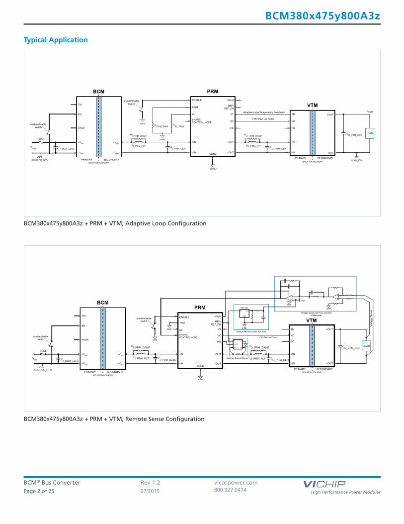
Typical Application
BCM380x475y800A3z + PRM + VTM, Adaptive Loop Configuration
External Current Sense
SGND
SGND
Voltage Reference with Soft Start
Voltage Sense and Error Amplifier(Differential)
VTM Start up Pulse
SGND
IN OUT
GND
V +
VOUT
–IN+IN
V –
PRM
ENABLE
TRIM
SHARE/CONTROL NODE
AL
IFB
VC
VT
VAUX
REF/REF_EN
+IN
–IN
+OUT
–OUT
SGND
SGND
TM
VC
PC
+IN
–IN –OUT
+OUT
ISOLATION BOUNDRY
VTM
PRIMARY SECONDARY
REF 3312 SGND
Volta
ge S
ense
SGND
LOAD
BCM
VAUX
EN
+VPRI
–VPRI
+VSEC
–VSEC
enable/disableswitch
FUSE
ISOLATION BOUNDRYPRIMARY SECONDARY
TM
VPRI CI_BCM_ELEC
SOURCE_RTN
SGND
CI_PRM_ELEC
RI_PRM_DAMP
LI_PRM_FLT
RO_PRM_DAMP
LO_PRM_FLT CO_PRM_CER
CO_VTM_CER
VREF
enable/disableswitch
BCM380x475y800A3z + PRM + VTM, Remote Sense Configuration
PRMENABLE
TRIM
SHARE/CONTROL NODE
AL
IFB
VC
VT
VAUX
REF/REF_EN
+IN
–IN
+OUT
–OUT
TM
VC
PC
+IN
–IN –OUT
+OUTAdaptive Loop Temperature Feedback
VTM Start Up Pulse
SGND
SGND
SGND
ISOLATION BOUNDRY LOAD_RTN
VTM
PRIMARY SECONDARY
BCM
VAUX
EN
+VPRI
–VPRI
+VSEC
–VSEC
enable/disableswitch
FUSE
ISOLATION BOUNDRYPRIMARY SECONDARY
TM
RI_PRM_CER
RTRIM_PRM RAL_PRM
SGND
CI_BCM_ELEC
SOURCE_RTN
VPRI
RI_PRM_DAMP
LI_PRM_FLT
RO_PRM_DAMP
LO_PRM_FLT CO_PRM_CER
LOAD
VOUT
CO_VTM_CER
enable/disableswitch
BCM® Bus Converter Rev 1.2 vicorpower.comPage 3 of 25 07/2015 800 927.9474
BCM380x475y800A3z
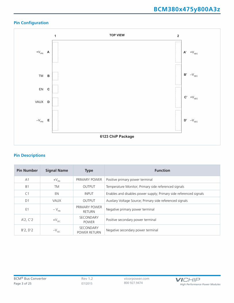
Pin Configuration
1 2
A
B
C
D
E D’
C’
B’
+VPRI +VSEC
TOP VIEW
6123 ChiP Package
A’
VAUX
EN
+VSEC
–VSEC
–VSEC–VPRI
TM
Pin Descriptions
Pin Number Signal Name Type Function
A1 +VPRI
PRIMARY POWER Positive primary power terminal
B1 TM OUTPUT Temperature Monitor; Primary side referenced signals
C1 EN INPUT Enables and disables power supply; Primary side referenced signals
D1 VAUX OUTPUT Auxilary Voltage Source; Primary side referenced signals
E1 – VPRI
PRIMARY POWER RETURN
Negative primary power terminal
A’2, C’2 +VSEC
SECONDARY POWER
Positive secondary power terminal
B’2, D’2 –VSEC
SECONDARY POWER RETURN
Negative secondary power terminal
BCM® Bus Converter Rev 1.2 vicorpower.comPage 4 of 25 07/2015 800 927.9474
BCM380x475y800A3z
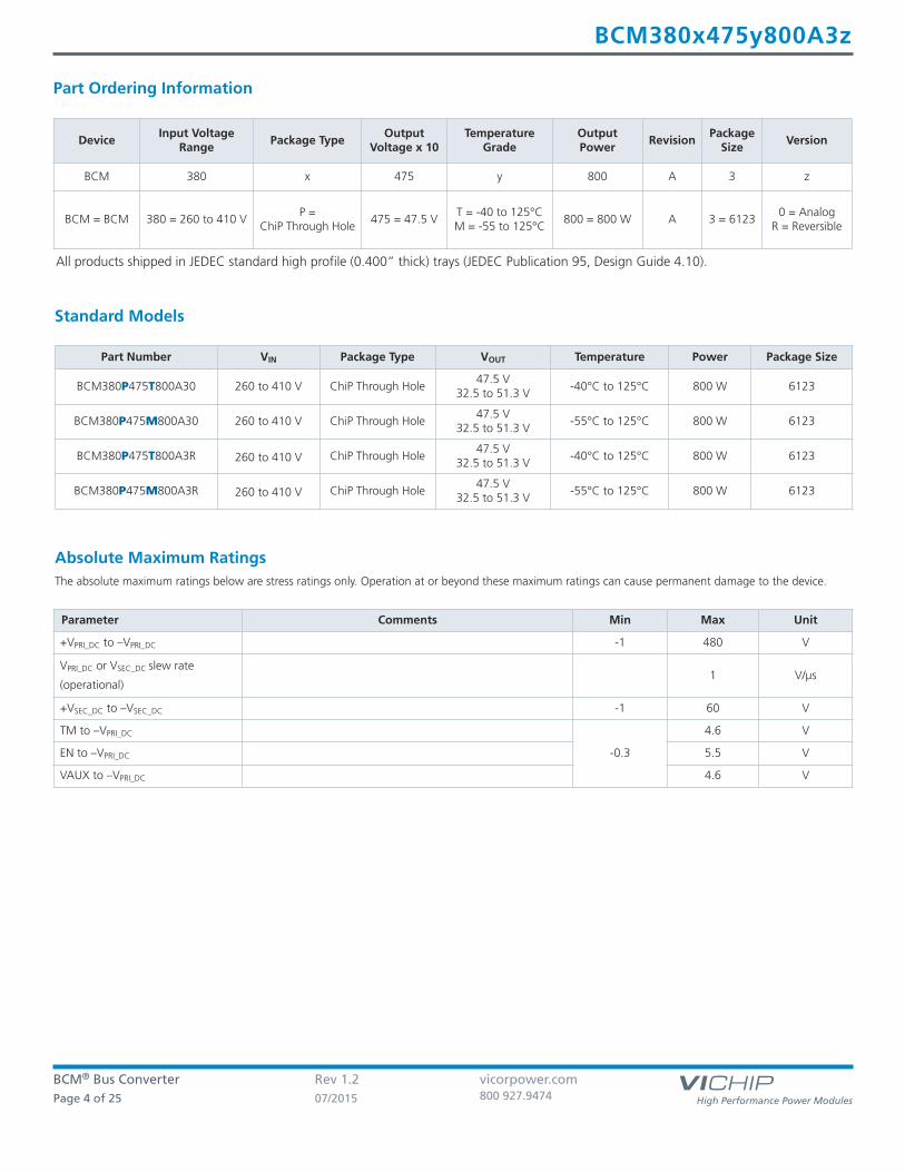
Absolute Maximum RatingsThe absolute maximum ratings below are stress ratings only. Operation at or beyond these maximum ratings can cause permanent damage to the device.
Parameter Comments Min Max Unit
+VPRI_DC to –VPRI_DC -1 480 V
VPRI_DC or VSEC_DC slew rate
(operational) 1 V/µs
+VSEC_DC to –VSEC_DC -1 60 V
TM to –VPRI_DC
-0.3
4.6 V
EN to –VPRI_DC 5.5 V
VAUX to –VPRI_DC 4.6 V
Part Ordering Information
DeviceInput Voltage
RangePackage Type
OutputVoltage x 10
TemperatureGrade
OutputPower
RevisionPackage
SizeVersion
BCM 380 x 475 y 800 A 3 z
BCM = BCM 380 = 260 to 410 V P =
ChiP Through Hole 475 = 47.5 V
T = -40 to 125 °C M = -55 to 125 °C
800 = 800 W A 3 = 6123 0 = Analog
R = Reversible
Standard Models
All products shipped in JEDEC standard high profile (0.400” thick) trays (JEDEC Publication 95, Design Guide 4.10).
Part Number VIN Package Type VOUT Temperature Power Package Size
BCM 380 P 475 T 800 A30 260 to 410 V ChiP Through Hole 47.5 V
32.5 to 51.3 V -40 °C to 125 °C 800 W 6123
BCM 380 P 475 M 800 A30 260 to 410 V ChiP Through Hole 47.5 V
32.5 to 51.3 V -55 °C to 125 °C 800 W 6123
BCM 380 P 475 T 800 A3R 260 to 410 V ChiP Through Hole 47.5 V
32.5 to 51.3 V -40 °C to 125 °C 800 W 6123
BCM 380 P 475 M 800 A3R 260 to 410 V ChiP Through Hole 47.5 V
32.5 to 51.3 V -55 °C to 125 °C 800 W 6123
BCM® Bus Converter Rev 1.2 vicorpower.comPage 5 of 25 07/2015 800 927.9474
BCM380x475y800A3z
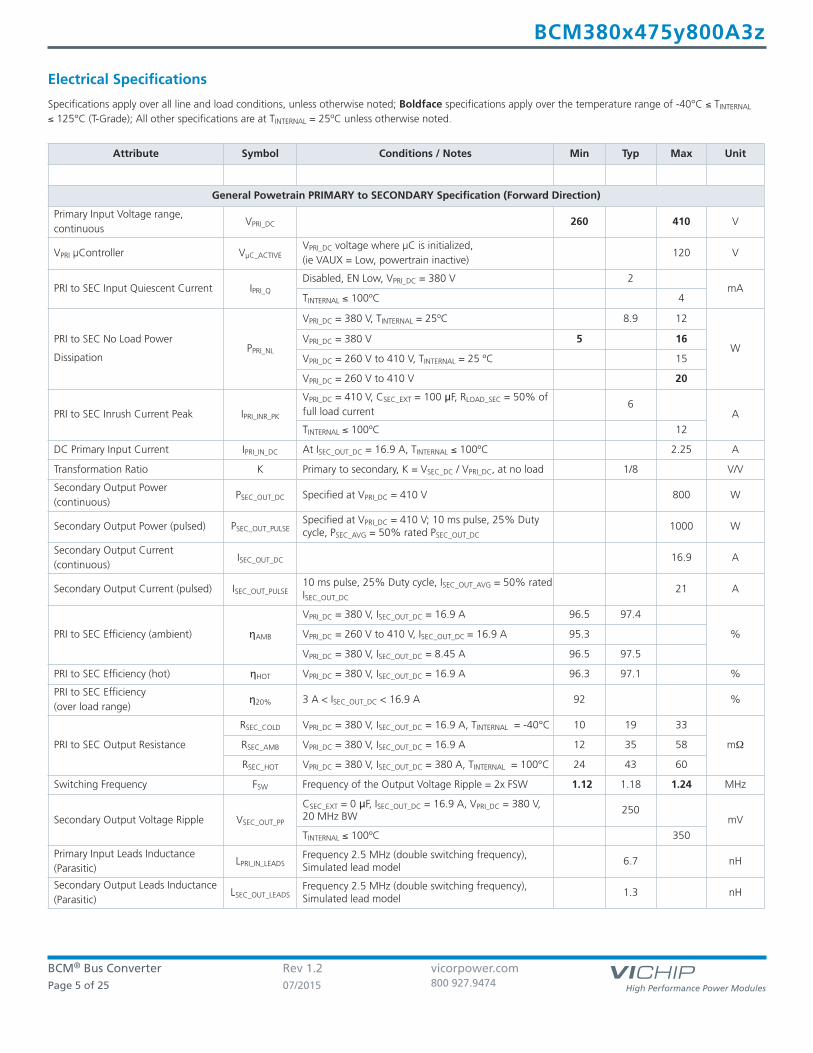
Electrical Specifications
Specifications apply over all line and load conditions, unless otherwise noted; Boldface specifications apply over the temperature range of -40 °C ≤ TINTERNAL
≤ 125 °C (T-Grade); All other specifications are at TINTERNAL = 25 ºC unless otherwise noted.
Attribute Symbol Conditions / Notes Min Typ Max Unit
General Powetrain PRIMARY to SECONDARY Specification (Forward Direction)
Primary Input Voltage range,continuous
VPRI_DC 260 410 V
VPRI µController VµC_ACTIVEVPRI_DC voltage where µC is initialized,(ie VAUX = Low, powertrain inactive)
120 V
PRI to SEC Input Quiescent Current IPRI_Q
Disabled, EN Low, VPRI_DC = 380 V 2 mA
TINTERNAL ≤ 100 ºC 4
PRI to SEC No Load Power
Dissipation PPRI_NL
VPRI_DC = 380 V, TINTERNAL = 25 ºC 8.9 12
WVPRI_DC = 380 V 5 16
VPRI_DC = 260 V to 410 V, TINTERNAL = 25 ºC 15
VPRI_DC = 260 V to 410 V 20
PRI to SEC Inrush Current Peak IPRI_INR_PK
VPRI_DC = 410 V, CSEC_EXT = 100 µF, RLOAD_SEC = 50 % offull load current
6 A
TINTERNAL ≤ 100 ºC 12
DC Primary Input Current IPRI_IN_DC At ISEC_OUT_DC = 16.9 A, TINTERNAL ≤ 100 ºC 2.25 A
Transformation Ratio K Primary to secondary, K = VSEC_DC / VPRI_DC, at no load 1/8 V/V
Secondary Output Power(continuous)
PSEC_OUT_DC Specified at VPRI_DC = 410 V 800 W
Secondary Output Power (pulsed) PSEC_OUT_PULSESpecified at VPRI_DC = 410 V; 10 ms pulse, 25% Dutycycle, PSEC_AVG = 50 % rated PSEC_OUT_DC
1000 W
Secondary Output Current(continuous)
ISEC_OUT_DC 16.9 A
Secondary Output Current (pulsed) ISEC_OUT_PULSE10 ms pulse, 25% Duty cycle, ISEC_OUT_AVG = 50 % ratedISEC_OUT_DC
21 A
PRI to SEC Efficiency (ambient) ηAMB
VPRI_DC = 380 V, ISEC_OUT_DC = 16.9 A 96.5 97.4
%VPRI_DC = 260 V to 410 V, ISEC_OUT_DC = 16.9 A 95.3
VPRI_DC = 380 V, ISEC_OUT_DC = 8.45 A 96.5 97.5
PRI to SEC Efficiency (hot) ηHOT VPRI_DC = 380 V, ISEC_OUT_DC = 16.9 A 96.3 97.1 %
PRI to SEC Efficiency(over load range)
η20% 3 A < ISEC_OUT_DC < 16.9 A 92 %
PRI to SEC Output Resistance
RSEC_COLD VPRI_DC = 380 V, ISEC_OUT_DC = 16.9 A, TINTERNAL = -40 °C 10 19 33
mΩRSEC_AMB VPRI_DC = 380 V, ISEC_OUT_DC = 16.9 A 12 35 58
RSEC_HOT VPRI_DC = 380 V, ISEC_OUT_DC = 380 A, TINTERNAL = 100 °C 24 43 60
Switching Frequency FSW Frequency of the Output Voltage Ripple = 2x FSW 1.12 1.18 1.24 MHz
Secondary Output Voltage Ripple VSEC_OUT_PP
CSEC_EXT = 0 µF, ISEC_OUT_DC = 16.9 A, VPRI_DC = 380 V,20 MHz BW
250 mV
TINTERNAL ≤ 100 ºC 350
Primary Input Leads Inductance(Parasitic)
LPRI_IN_LEADSFrequency 2.5 MHz (double switching frequency),Simulated lead model
6.7 nH
Secondary Output Leads Inductance(Parasitic)
LSEC_OUT_LEADSFrequency 2.5 MHz (double switching frequency),Simulated lead model
1.3 nH
BCM® Bus Converter Rev 1.2 vicorpower.comPage 6 of 25 07/2015 800 927.9474
BCM380x475y800A3z
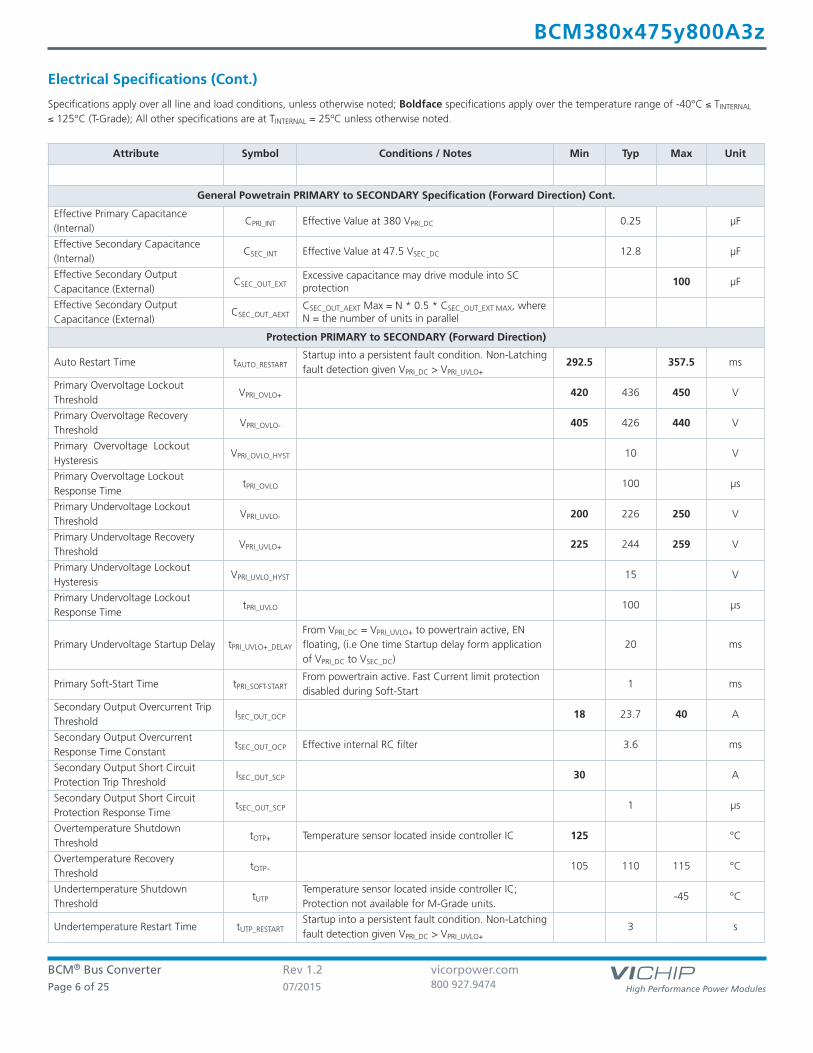
Electrical Specifications (Cont.)
Specifications apply over all line and load conditions, unless otherwise noted; Boldface specifications apply over the temperature range of -40 °C ≤ TINTERNAL
≤ 125 °C (T-Grade); All other specifications are at TINTERNAL = 25 ºC unless otherwise noted.
Attribute Symbol Conditions / Notes Min Typ Max Unit
General Powetrain PRIMARY to SECONDARY Specification (Forward Direction) Cont.
Effective Primary Capacitance(Internal)
CPRI_INT Effective Value at 380 VPRI_DC 0.25 µF
Effective Secondary Capacitance(Internal)
CSEC_INT Effective Value at 47.5 VSEC_DC 12.8 µF
Effective Secondary OutputCapacitance (External)
CSEC_OUT_EXTExcessive capacitance may drive module into SCprotection
100 µF
Effective Secondary OutputCapacitance (External)
CSEC_OUT_AEXTCSEC_OUT_AEXT Max = N * 0.5 * CSEC_OUT_EXT MAX, whereN = the number of units in parallel
Protection PRIMARY to SECONDARY (Forward Direction)
Auto Restart Time tAUTO_RESTARTStartup into a persistent fault condition. Non-Latchingfault detection given VPRI_DC > VPRI_UVLO+
292.5 357.5 ms
Primary Overvoltage LockoutThreshold
VPRI_OVLO+ 420 436 450 V
Primary Overvoltage RecoveryThreshold
VPRI_OVLO- 405 426 440 V
Primary Overvoltage LockoutHysteresis
VPRI_OVLO_HYST 10 V
Primary Overvoltage LockoutResponse Time
tPRI_OVLO 100 µs
Primary Undervoltage LockoutThreshold
VPRI_UVLO- 200 226 250 V
Primary Undervoltage RecoveryThreshold
VPRI_UVLO+ 225 244 259 V
Primary Undervoltage LockoutHysteresis
VPRI_UVLO_HYST 15 V
Primary Undervoltage LockoutResponse Time
tPRI_UVLO 100 µs
Primary Undervoltage Startup Delay tPRI_UVLO+_DELAY
From VPRI_DC = VPRI_UVLO+ to powertrain active, ENfloating, (i.e One time Startup delay form applicationof VPRI_DC to VSEC_DC)
20 ms
Primary Soft-Start Time tPRI_SOFT-STARTFrom powertrain active. Fast Current limit protectiondisabled during Soft-Start
1 ms
Secondary Output Overcurrent TripThreshold
ISEC_OUT_OCP 18 23.7 40 A
Secondary Output OvercurrentResponse Time Constant
tSEC_OUT_OCP Effective internal RC filter 3.6 ms
Secondary Output Short CircuitProtection Trip Threshold
ISEC_OUT_SCP 30 A
Secondary Output Short CircuitProtection Response Time
tSEC_OUT_SCP 1 µs
Overtemperature ShutdownThreshold
tOTP+ Temperature sensor located inside controller IC 125 °C
Overtemperature RecoveryThreshold
tOTP– 105 110 115 °C
Undertemperature ShutdownThreshold
tUTPTemperature sensor located inside controller IC;Protection not available for M-Grade units.
-45 °C
Undertemperature Restart Time tUTP_RESTARTStartup into a persistent fault condition. Non-Latchingfault detection given VPRI_DC > VPRI_UVLO+
3 s
BCM® Bus Converter Rev 1.2 vicorpower.comPage 7 of 25 07/2015 800 927.9474
BCM380x475y800A3z
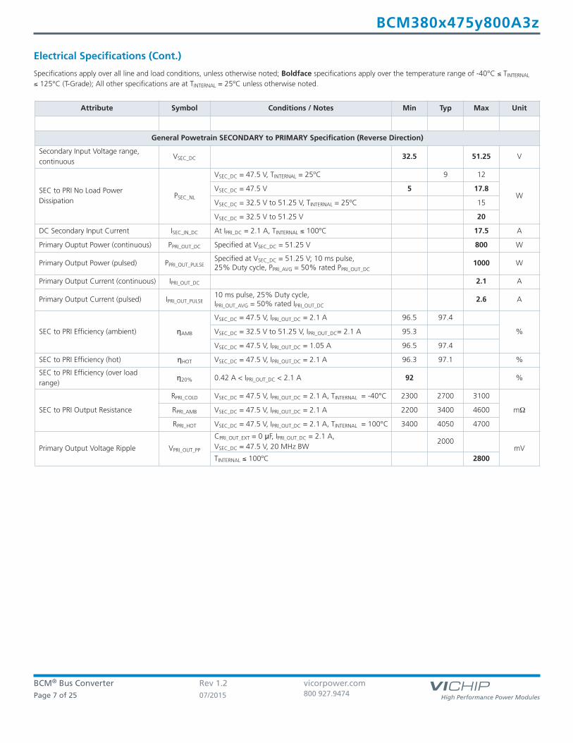
Attribute Symbol Conditions / Notes Min Typ Max Unit
General Powetrain SECONDARY to PRIMARY Specification (Reverse Direction)
Secondary Input Voltage range,continuous
VSEC_DC 32.5 51.25 V
SEC to PRI No Load PowerDissipation
PSEC_NL
VSEC_DC = 47.5 V, TINTERNAL = 25ºC 9 12
WVSEC_DC = 47.5 V 5 17.8
VSEC_DC = 32.5 V to 51.25 V, TINTERNAL = 25ºC 15
VSEC_DC = 32.5 V to 51.25 V 20
DC Secondary Input Current ISEC_IN_DC At IPRI_DC = 2.1 A, TINTERNAL ≤ 100ºC 17.5 A
Primary Ouptut Power (continuous) PPRI_OUT_DC Specified at VSEC_DC = 51.25 V 800 W
Primary Output Power (pulsed) PPRI_OUT_PULSESpecified at VSEC_DC = 51.25 V; 10 ms pulse,25% Duty cycle, PPRI_AVG = 50 % rated PPRI_OUT_DC
1000 W
Primary Output Current (continuous) IPRI_OUT_DC 2.1 A
Primary Output Current (pulsed) IPRI_OUT_PULSE10 ms pulse, 25% Duty cycle,IPRI_OUT_AVG = 50 % rated IPRI_OUT_DC
2.6 A
SEC to PRI Efficiency (ambient) ηAMB
VSEC_DC = 47.5 V, IPRI_OUT_DC = 2.1 A 96.5 97.4
%VSEC_DC = 32.5 V to 51.25 V, IPRI_OUT_DC= 2.1 A 95.3
VSEC_DC = 47.5 V, IPRI_OUT_DC = 1.05 A 96.5 97.4
SEC to PRI Efficiency (hot) ηHOT VSEC_DC = 47.5 V, IPRI_OUT_DC = 2.1 A 96.3 97.1 %
SEC to PRI Efficiency (over loadrange)
η20% 0.42 A < IPRI_OUT_DC < 2.1 A 92 %
SEC to PRI Output Resistance
RPRI_COLD VSEC_DC = 47.5 V, IPRI_OUT_DC = 2.1 A, TINTERNAL = -40°C 2300 2700 3100
mΩRPRI_AMB VSEC_DC = 47.5 V, IPRI_OUT_DC = 2.1 A 2200 3400 4600
RPRI_HOT VSEC_DC = 47.5 V, IPRI_OUT_DC = 2.1 A, TINTERNAL = 100°C 3400 4050 4700
Primary Output Voltage Ripple VPRI_OUT_PP
CPRI_OUT_EXT = 0 µF, IPRI_OUT_DC = 2.1 A,VSEC_DC = 47.5 V, 20 MHz BW
2000 mV
TINTERNAL ≤ 100ºC 2800
Electrical Specifications (Cont.)
Specifications apply over all line and load conditions, unless otherwise noted; Boldface specifications apply over the temperature range of -40 °C ≤ TINTERNAL
≤ 125 °C (T-Grade); All other specifications are at TINTERNAL = 25 ºC unless otherwise noted.
BCM® Bus Converter Rev 1.2 vicorpower.comPage 8 of 25 07/2015 800 927.9474
BCM380x475y800A3z
Attribute Symbol Conditions / Notes Min Typ Max Unit
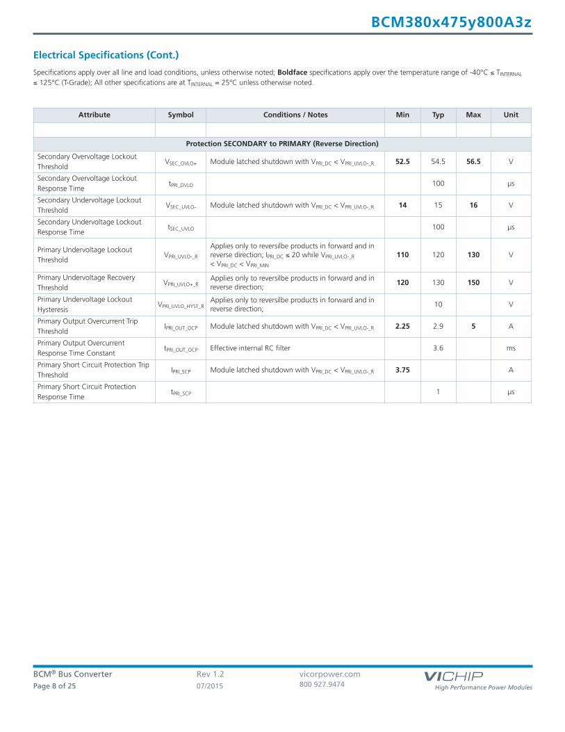
Protection SECONDARY to PRIMARY (Reverse Direction)
Secondary Overvoltage LockoutThreshold
VSEC_OVLO+ Module latched shutdown with VPRI_DC < VPRI_UVLO-_R 52.5 54.5 56.5 V
Secondary Overvoltage LockoutResponse Time
tPRI_OVLO 100 µs
Secondary Undervoltage LockoutThreshold
VSEC_UVLO- Module latched shutdown with VPRI_DC < VPRI_UVLO-_R 14 15 16 V
Secondary Undervoltage LockoutResponse Time
tSEC_UVLO 100 µs
Primary Undervoltage LockoutThreshold
VPRI_UVLO-_R
Applies only to reversilbe products in forward and inreverse direction; IPRI_DC ≤ 20 while VPRI_UVLO-_R
< VPRI_DC < VPRI_MIN
110 120 130 V
Primary Undervoltage RecoveryThreshold
VPRI_UVLO+_RApplies only to reversilbe products in forward and inreverse direction;
120 130 150 V
Primary Undervoltage LockoutHysteresis
VPRI_UVLO_HYST_RApplies only to reversilbe products in forward and inreverse direction;
10 V
Primary Output Overcurrent TripThreshold
IPRI_OUT_OCP Module latched shutdown with VPRI_DC < VPRI_UVLO-_R 2.25 2.9 5 A
Primary Output OvercurrentResponse Time Constant
tPRI_OUT_OCP Effective internal RC filter 3.6 ms
Primary Short Circuit Protection TripThreshold
IPRI_SCP Module latched shutdown with VPRI_DC < VPRI_UVLO-_R 3.75 A
Primary Short Circuit ProtectionResponse Time
tPRI_SCP 1 µs
Electrical Specifications (Cont.)
Specifications apply over all line and load conditions, unless otherwise noted; Boldface specifications apply over the temperature range of -40 °C ≤ TINTERNAL
≤ 125 °C (T-Grade); All other specifications are at TINTERNAL = 25 ºC unless otherwise noted.
BCM® Bus Converter Rev 1.2 vicorpower.comPage 9 of 25 07/2015 800 927.9474
BCM® Bus Converter Rev 1.2 vicorpower.comPage 9 of 25 07/2015 800 927.9474
BCM380x475y800A3z
Seon
dary
Out
put C
urre
nt (A
)
Primary Input Voltage (V) ISEC_OUT_DC ISEC_OUT_PULSE
10
12
14
16
18
20
22
260 275 290 305 320 335 350 365 380 395 410
Seon
dary
Out
put P
ower
(W)
Primary Input Voltage (V) PSEC_OUT_DC PSEC_OUT_PULSE
300
400
500
600
700
800
900
1000
1100
260 275 290 305 320 335 350 365 380 395 410
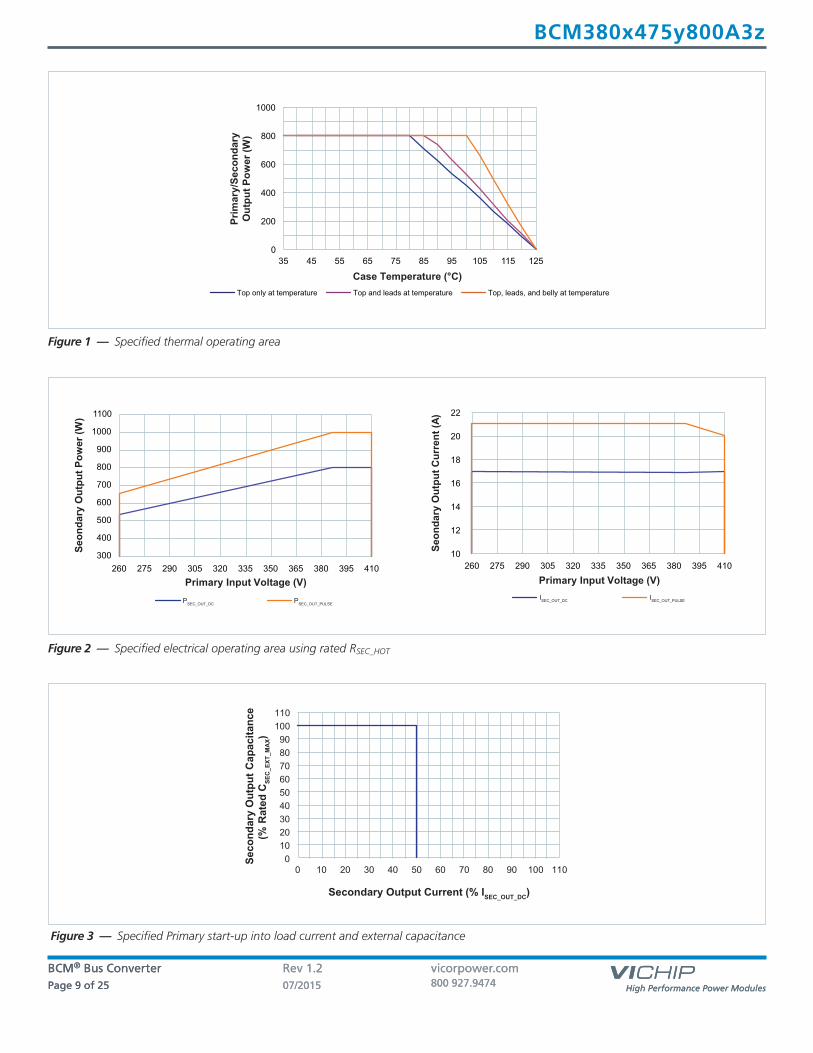
Figure 1 — Specified thermal operating area
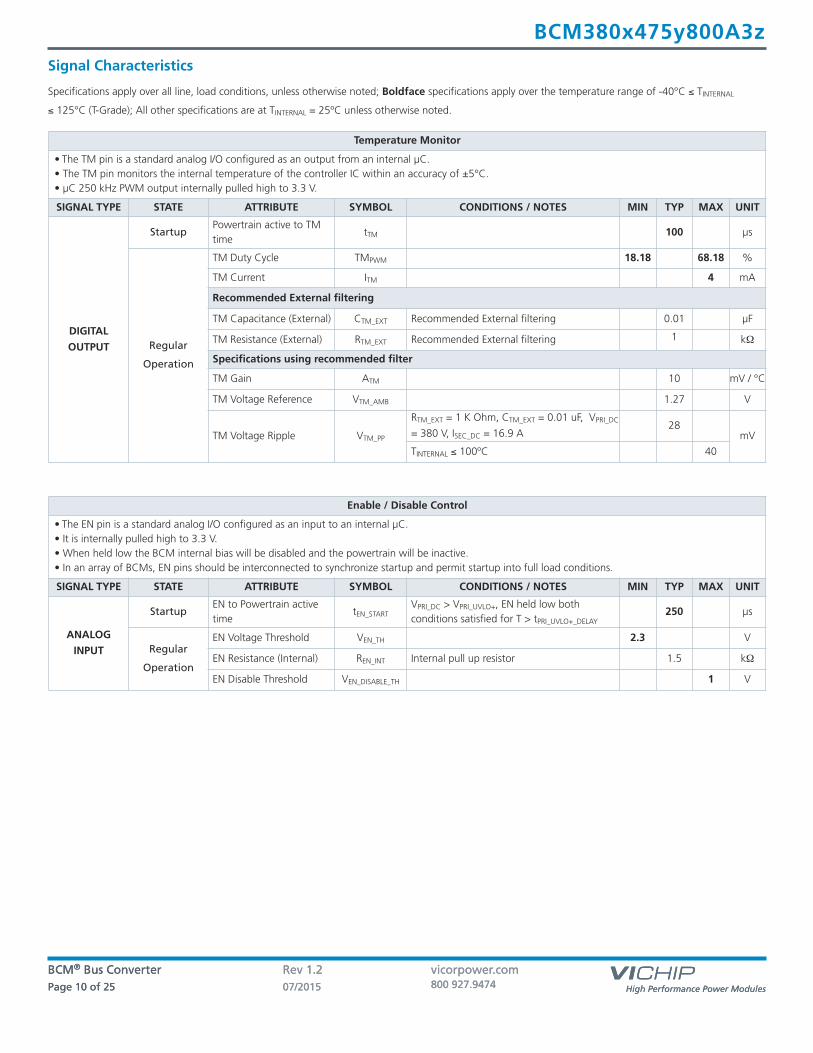
Figure 2 — Specified electrical operating area using rated RSEC_HOT
0102030405060708090
100110
0 10 20 30 40 50 60 70 80 90 100 110
Seco
ndar
y O
utpu
t Cap
acita
nce
(% R
ated
CSE
C_E
XT_M
AX)
Secondary Output Current (% ISEC_OUT_DC)
Prim
ary/
Seco
ndar
yO
utpu
t Pow
er (W
)
Case Temperature (°C)
0
200
400
600
800
1000
35 45 55 65 75 85 95 105 115 125
Top only at temperature Top and leads at temperature Top, leads, and belly at temperature
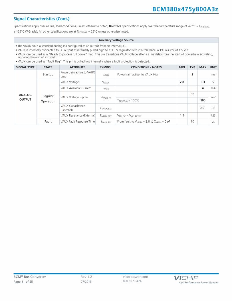
Figure 3 — Specified Primary start-up into load current and external capacitance
BCM® Bus Converter Rev 1.2 vicorpower.comPage 10 of 25 07/2015 800 927.9474
BCM® Bus Converter Rev 1.2 vicorpower.comPage 10 of 25 07/2015 800 927.9474
BCM380x475y800A3z
Signal Characteristics
Specifications apply over all line, load conditions, unless otherwise noted; Boldface specifications apply over the temperature range of -40 °C ≤ TINTERNAL
≤ 125 °C (T-Grade); All other specifications are at TINTERNAL = 25 ºC unless otherwise noted.
Temperature Monitor
• The TM pin is a standard analog I/O configured as an output from an internal µC.• The TM pin monitors the internal temperature of the controller IC within an accuracy of ±5°C.• µC 250 kHz PWM output internally pulled high to 3.3 V.
SIGNAL TYPE STATE ATTRIBUTE SYMBOL CONDITIONS / NOTES MIN TYP MAX UNIT
DIGITAL
OUTPUT
StartupPowertrain active to TMtime
tTM 100 µs
Regular
Operation
TM Duty Cycle TMPWM 18.18 68.18 %
TM Current ITM 4 mA
Recommended External filtering
TM Capacitance (External) CTM_EXT Recommended External filtering 0.01 µF
TM Resistance (External) RTM_EXT Recommended External filtering 1 kΩ
Specifications using recommended filter
TM Gain ATM 10 mV / °C
TM Voltage Reference VTM_AMB 1.27 V
TM Voltage Ripple VTM_PP
RTM_EXT = 1 K Ohm, CTM_EXT = 0.01 uF, VPRI_DC
= 380 V, ISEC_DC = 16.9 A 28
mV
TINTERNAL ≤ 100ºC 40
Enable / Disable Control
• The EN pin is a standard analog I/O configured as an input to an internal µC. • It is internally pulled high to 3.3 V.• When held low the BCM internal bias will be disabled and the powertrain will be inactive. • In an array of BCMs, EN pins should be interconnected to synchronize startup and permit startup into full load conditions.
SIGNAL TYPE STATE ATTRIBUTE SYMBOL CONDITIONS / NOTES MIN TYP MAX UNIT
ANALOG
INPUT
StartupEN to Powertrain activetime
tEN_STARTVPRI_DC > VPRI_UVLO+, EN held low bothconditions satisfied for T > tPRI_UVLO+_DELAY
250 µs
Regular
Operation
EN Voltage Threshold VEN_TH 2.3 V
EN Resistance (Internal) REN_INT Internal pull up resistor 1.5 kΩ
EN Disable Threshold VEN_DISABLE_TH 1 V
BCM® Bus Converter Rev 1.2 vicorpower.comPage 11 of 25 07/2015 800 927.9474
BCM380x475y800A3z
Auxiliary Voltage Source
• The VAUX pin is a standard analog I/O configured as an output from an internal µC.• VAUX is internally connected to µC output as internally pulled high to a 3.3 V regulator with 2% tolerance, a 1% resistor of 1.5 kΩ.• VAUX can be used as a "Ready to process full power" flag. This pin transitions VAUX voltage after a 2 ms delay from the start of powertrain activating,
signaling the end of softstart.• VAUX can be used as "Fault flag". This pin is pulled low internally when a fault protection is detected.
SIGNAL TYPE STATE ATTRIBUTE SYMBOL CONDITIONS / NOTES MIN TYP MAX UNIT
ANALOG
OUTPUT
StartupPowertrain active to VAUXtime
tVAUX Powertrain active to VAUX High 2 ms
Regular
Operation
VAUX Voltage VVAUX 2.8 3.3 V
VAUX Available Current IVAUX 4 mA
VAUX Voltage Ripple VVAUX_PP
50 mV
TINTERNAL ≤ 100ºC 100
VAUX Capacitance(External)
CVAUX_EXT 0.01 µF
VAUX Resistance (External) RVAUX_EXT VPRI_DC < VµC_ACTIVE 1.5 kΩ
Fault VAUX Fault Response Time tVAUX_FR From fault to VVAUX = 2.8 V, CVAUX = 0 pF 10 µs
Signal Characteristics (Cont.)
Specifications apply over all line, load conditions, unless otherwise noted; Boldface specifications apply over the temperature range of -40 °C ≤ TINTERNAL
≤ 125 °C (T-Grade); All other specifications are at TINTERNAL = 25 ºC unless otherwise noted.
BCM® Bus Converter Rev 1.2 vicorpower.comPage 12 of 25 07/2015 800 927.9474
BCM380x475y800A3z
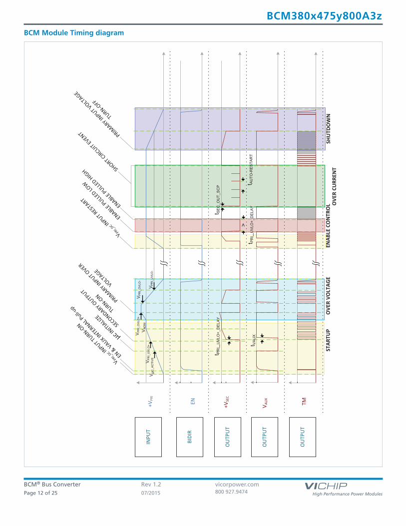
BCM Module Timing diagram
EN TM+VPR
I
BIDI
R
INPU
T
+VSE
C
OU
TPU
T
VPRI_DCINPUT TURN-O
N SECONDARY O
UTPUT
TURN-ON
PRIMARY IN
PUT OVER
VOLTAGE
VPRI_DCINPUT REST
ART
ENABLE PULLE
D LOW
ENABLE PULLE
D HIGH SHORT CIRCUIT EVENT PRIM
ARY INPUT VOLT
AGE
TURN-OFF
OU
TPU
T
OU
TPU
T
V AU
X
EN & VAUX IN
TERNAL Pull-u
p
STAR
TUP
OVE
R VO
LTAG
EEN
ABLE
CO
NTR
OL O
VER
CURR
ENT
SHU
TDO
WN
µcINITIALIZ
E
VPR
I_O
VLO
-V
PRI_
OVL
O+
VPR
I_U
VLO
+V
µC_A
CTI
VE
VN
OM
V PR
I_U
VLO
-
t SE
C_O
UT_
SC
Pt P
RI_
UV
LO+_
DE
LAY
t VA
UX
t AU
TO-R
ESTA
RT
> t P
RI_
UVL
O+_
DE
LAY
BCM® Bus Converter Rev 1.2 vicorpower.comPage 13 of 25 07/2015 800 927.9474
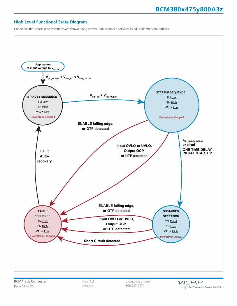
BCM380x475y800A3z
FAULT
SEQUENCE
TM Low
EN High
VAUX Low
Powertrain Stopped
VμC_ACTIVE < VPRI_DC < VPRI_UVLO+
VPRI_DC > VPRI_UVLO+
tPRI_UVLO+_DELAY
expiredONE TIME DELAYINITIAL STARTUPFault
Auto-recovery
ENABLE falling edge,or OTP detected
Input OVLO or UVLO,Output OCP,
or UTP detected
ENABLE falling edge,or OTP detected
Input OVLO or UVLO,Output OCP,
or UTP detected
Short Circuit detected
Applicationof input voltage to VPRI_DC
SUSTAINED
OPERATION
TM PWM
EN High
VAUX High
Powertrain Active
STARTUP SEQUENCE
TM Low
EN High
VAUX Low
Powertrain Stopped
STANDBY SEQUENCE
TM Low
EN High
VAUX Low
Powertrain Stopped
High Level Functional State Diagram
Conditions that cause state transitions are shown along arrows. Sub-sequence activities listed inside the state bubbles.
BCM® Bus Converter Rev 1.2 vicorpower.comPage 14 of 25 07/2015 800 927.9474
BCM380x475y800A3z
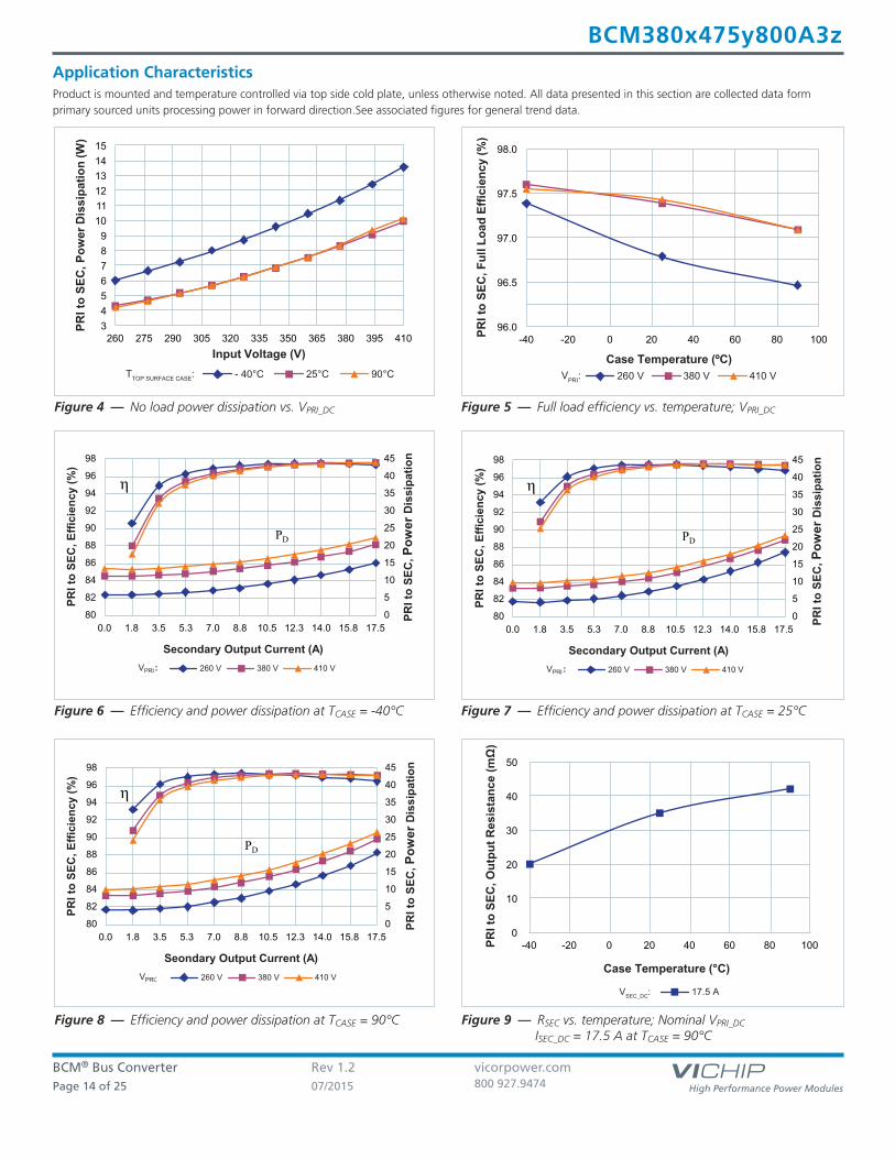
Application CharacteristicsProduct is mounted and temperature controlled via top side cold plate, unless otherwise noted. All data presented in this section are collected data formprimary sourced units processing power in forward direction.See associated figures for general trend data.
PRI t
o SE
C, P
ower
Dis
sipa
tion
(W)
Input Voltage (V) - 40°C 25°C 90°CTTOP SURFACE CASE:
3 4 5 6 7 8 9
10 11 12 13 14 15
260 275 290 305 320 335 350 365 380 395 410
Case Temperature (ºC) 260 V 380 V 410 V
PRI t
o SE
C, F
ull L
oad
Effic
ienc
y (%
)
VPRI:
96.0
96.5
97.0
97.5
98.0
-40 -20 0 20 40 60 80 100
PRI t
o SE
C, E
ffici
ency
(%)
PRI t
o SE
C, P
ower
Dis
sipa
tion
Secondary Output Current (A) 260 V 380 V 410 VVPRI :
0
5
10
15
20
25
30
35
40
45
80
82
84
86
88
90
92
94
96
98
0.0 1.8 3.5 5.3 7.0 8.8 10.5 12.3 14.0 15.8 17.5
PD
Figure 4 — No load power dissipation vs. VPRI_DC Figure 5 — Full load efficiency vs. temperature; VPRI_DC
Figure 6 — Efficiency and power dissipation at TCASE = -40 °C
PRI t
o SE
C, E
ffici
ency
(%)
Secondary Output Current (A) 260 V 380 V 410 VVPRI :
0
5
10
15
20
25
30
35
40
45
80
82
84
86
88
90
92
94
96
98
0.0 1.8 3.5 5.3 7.0 8.8 10.5 12.3 14.0 15.8 17.5
PD
PRI t
o SE
C, P
ower
Dis
sipa
tion
PRI t
o SE
C, P
ower
Dis
sipa
tion
Seondary Output Current (A) 260 V 380 V 410 VVPRI:
0
5
10
15
20
25
30
35
40
45
80
82
84
86
88
90
92
94
96
98
0.0 1.8 3.5 5.3 7.0 8.8 10.5 12.3 14.0 15.8 17.5
PD
PRI t
o SE
C, E
ffici
ency
(%)
Figure 7 — Efficiency and power dissipation at TCASE = 25 °C
Case Temperature (°C)
17.5 AVSEC_DC:
0
10
20
30
40
50
-40 -20 0 20 40 60 80 100 PRI t
o SE
C, O
utpu
t Res
ista
nce
(mΩ
)
Figure 8 — Efficiency and power dissipation at TCASE = 90 °C Figure 9 — RSEC vs. temperature; Nominal VPRI_DC
ISEC_DC = 17.5 A at TCASE = 90 °C
BCM® Bus Converter Rev 1.2 vicorpower.comPage 15 of 25 07/2015 800 927.9474
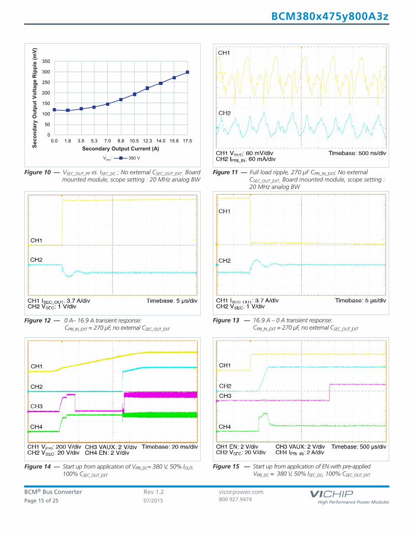
BCM380x475y800A3z
Figure 12 — 0 A– 16.9 A transient response:CPRI_IN_EXT = 270 µF, no external CSEC_OUT_EXT
Figure 11 — Full load ripple, 270 µF CPRI_IN_EXT; No externalCSEC_OUT_EXT. Board mounted module, scope setting : 20 MHz analog BW
Secondary Output Current (A) 380 VVPRI:
0
50
100
150
200
250
300
350
0.0 1.8 3.5 5.3 7.0 8.8 10.5 12.3 14.0 15.8 17.5
Seco
ndar
y O
utpu
t Vol
tage
Rip
ple
(mV)
Figure 10 — VSEC_OUT_PP vs. ISEC_DC ; No external CSEC_OUT_EXT. Boardmounted module, scope setting : 20 MHz analog BW
Figure 13 — 16.9 A – 0 A transient response: CPRI_IN_EXT = 270 µF, no external CSEC_OUT_EXT
Figure 14 — Start up from application of VPRI_DC= 380 V, 50 % IOUT,100% CSEC_OUT_EXT
Figure 15 — Start up from application of EN with pre-applied VPRI_DC = 380 V, 50 % ISEC_DC, 100% CSEC_OUT_EXT
BCM® Bus Converter Rev 1.2 vicorpower.comPage 16 of 25 07/2015 800 927.9474
BCM380x475y800A3z
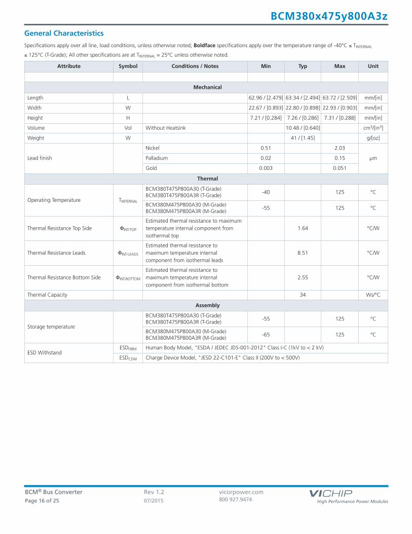
General Characteristics
Specifications apply over all line, load conditions, unless otherwise noted; Boldface specifications apply over the temperature range of -40 °C ≤ TINTERNAL
≤ 125 °C (T-Grade); All other specifications are at TINTERNAL = 25 ºC unless otherwise noted.
Attribute Symbol Conditions / Notes Min Typ Max Unit
Mechanical
Length L 62.96 / [2.479] 63.34 / [2.494] 63.72 / [2.509] mm/[in]
Width W 22.67 / [0.893] 22.80 / [0.898] 22.93 / [0.903] mm/[in]
Height H 7.21 / [0.284] 7.26 / [0.286] 7.31 / [0.288] mm/[in]
Volume Vol Without Heatsink 10.48 / [0.640] cm3/[in3]
Weight W 41 / [1.45] g/[oz]
Lead finish
Nickel 0.51 2.03
µmPalladium 0.02 0.15
Gold 0.003 0.051
Thermal
Operating Temperature TINTERNAL
BCM380T475P800A30 (T-Grade) BCM380T475P800A3R (T-Grade)
-40 125 °C
BCM380M475P800A30 (M-Grade) BCM380M475P800A3R (M-Grade)
-55 125 °C
Thermal Resistance Top Side ΦINT-TOP
Estimated thermal resistance to maximumtemperature internal component fromisothermal top
1.64 °C/W
Thermal Resistance Leads ΦINT-LEADS
Estimated thermal resistance tomaximum temperature internalcomponent from isothermal leads
8.51 °C/W
Thermal Resistance Bottom Side ΦINT-BOTTOM
Estimated thermal resistance tomaximum temperature internalcomponent from isothermal bottom
2.55 °C/W
Thermal Capacity 34 Ws/°C
Assembly
Storage temperature
BCM380T475P800A30 (T-Grade) BCM380T475P800A3R (T-Grade)
-55 125 °C
BCM380M475P800A30 (M-Grade) BCM380M475P800A3R (M-Grade)
-65 125 °C
ESD WithstandESDHBM Human Body Model, "ESDA / JEDEC JDS-001-2012" Class I-C (1kV to < 2 kV)
ESDCDM Charge Device Model, "JESD 22-C101-E" Class II (200V to < 500V)
BCM® Bus Converter Rev 1.2 vicorpower.comPage 17 of 25 07/2015 800 927.9474
BCM380x475y800A3z
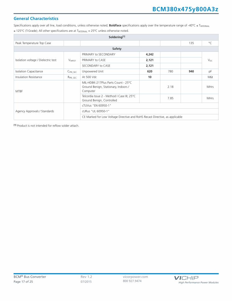
[1] Product is not intended for reflow solder attach.
General Characteristics
Specifications apply over all line, load conditions, unless otherwise noted; Boldface specifications apply over the temperature range of -40 °C ≤ TINTERNAL
≤ 125 °C (T-Grade); All other specifications are at TINTERNAL = 25 ºC unless otherwise noted.
Soldering[1]
Peak Temperature Top Case 135 °C
Safety
Isolation voltage / Dielectric test VHIPOT
PRIMARY to SECONDARY 4,242
VDCPRIMARY to CASE 2,121
SECONDARY to CASE 2,121
Isolation Capacitance CPRI_SEC Unpowered Unit 620 780 940 pF
Insulation Resistance RPRI_SEC At 500 Vdc 10 MΩ
MTBF
MIL-HDBK-217Plus Parts Count - 25°CGround Benign, Stationary, Indoors /Computer
2.18 MHrs
Telcordia Issue 2 - Method I Case III; 25°CGround Benign, Controlled
7.85 MHrs
Agency Approvals / Standards
cTUVus "EN 60950-1"
cURus "UL 60950-1"
CE Marked for Low Voltage Directive and RoHS Recast Directive, as applicable
BCM® Bus Converter Rev 1.2 vicorpower.comPage 18 of 25 07/2015 800 927.9474
BCM380x475y800A3z
C01
C02
Q01
C03
C04
C05
C06
C07
C08
C09
C10
L01
Current Flow detection+ Forward IPRI_DC sense
I PR
I_D
C
Star
tup
Circ
uit
+VPR
I /4
SEPI
C E
N
Cr
CO
UT
+VSE
C
-VSE
C
+VPR
I
-VPR
I
ENTM P
WM
TM
EN
VAU
X
Diff
eren
tial C
urre
nt
Sens
ing
Full-
Brid
ge S
ynch
rono
us
Rec
tific
atio
n
Prim
ary
Stag
e
Fast
Cur
rent
Li
mit
Analog Controller
Digital Controller
SEPI
C
Cnt
rlO
n/O
ff
Q02
Q03
Q04
Q05
Q06
Q07
Q08
Lr
Seco
ndar
y St
age
Q11
Q12
Q09
Q10
+Vcc
-VC
C
3.3v
Li
near
R
egul
ator
+VPR
I /4
( +V P
RI /4
) -X
Slow
Cur
rent
Li
mit
Mod
ulat
or
Prim
ary
and
Seco
ndar
y G
ate
Driv
e Tr
ansf
orm
er
1.5
kΩ
1.5
kΩ
Soft-
Star
t
VAU
X
Ove
r-Te
mp
Und
er-T
emp
Ove
r Vol
tage
U
nder
Volta
ge
Star
tup
/R
e-st
art D
elay
Tem
pera
ture
Se
nsor
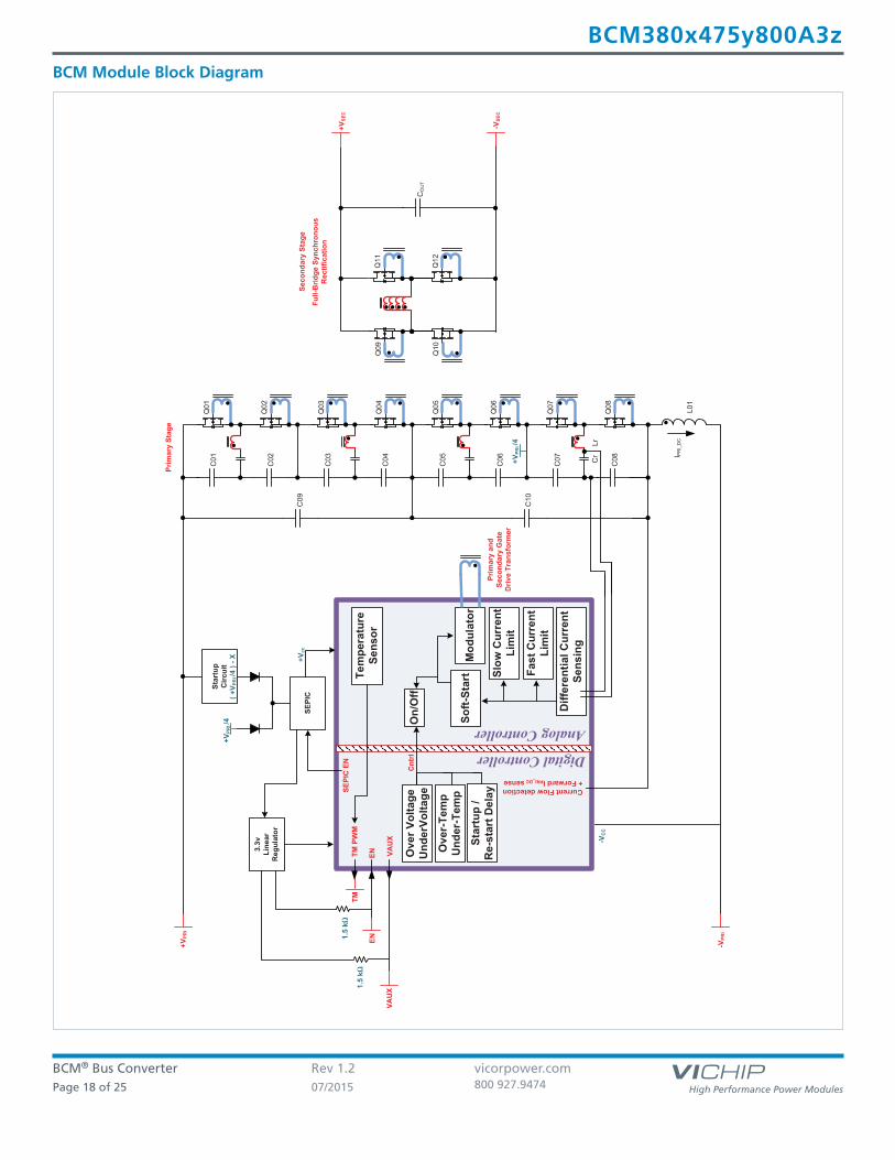
BCM Module Block Diagram
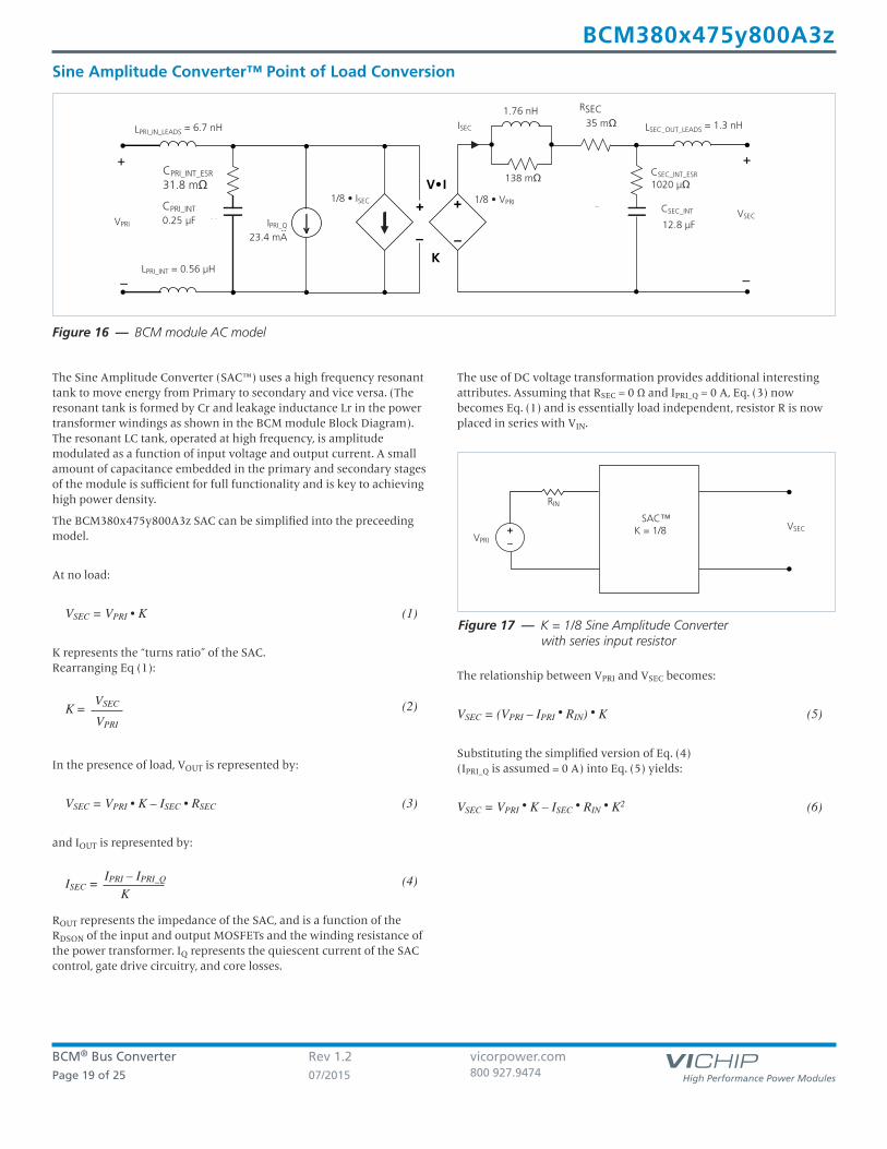
The Sine Amplitude Converter (SAC™) uses a high frequency resonanttank to move energy from Primary to secondary and vice versa. (Theresonant tank is formed by Cr and leakage inductance Lr in the powertransformer windings as shown in the BCM module Block Diagram).The resonant LC tank, operated at high frequency, is amplitudemodulated as a function of input voltage and output current. A smallamount of capacitance embedded in the primary and secondary stagesof the module is sufficient for full functionality and is key to achievinghigh power density.
The BCM380x475y800A3z SAC can be simplified into the preceedingmodel.
At no load:
VSEC = VPRI • K (1)
K represents the “turns ratio” of the SAC. Rearranging Eq (1):
K =VSEC (2)VPRI
In the presence of load, VOUT is represented by:
VSEC = VPRI • K – ISEC • RSEC (3)
and IOUT is represented by:
ISEC = IPRI – IPRI_Q (4)
K
ROUT represents the impedance of the SAC, and is a function of theRDSON of the input and output MOSFETs and the winding resistance ofthe power transformer. IQ represents the quiescent current of the SACcontrol, gate drive circuitry, and core losses.
The use of DC voltage transformation provides additional interestingattributes. Assuming that RSEC = 0 Ω and IPRI_Q = 0 A, Eq. (3) nowbecomes Eq. (1) and is essentially load independent, resistor R is nowplaced in series with VIN.
The relationship between VPRI and VSEC becomes:
VSEC = (VPRI – IPRI • RIN) • K (5)
Substituting the simplified version of Eq. (4) (IPRI_Q is assumed = 0 A) into Eq. (5) yields:
VSEC = VPRI • K – ISEC • RIN • K2 (6)
BCM® Bus Converter Rev 1.2 vicorpower.comPage 19 of 25 07/2015 800 927.9474
BCM380x475y800A3z
+
–
+
–
VOUT
COUTVIN
V•I
K
+
–
+
–
CIN
IOUT
RCOUT
IQ
ROUT
RCIN
23.4 mA
1/8 • ISEC 1/8 • VPRI
CPRI_INT_ESR
31.8 mΩ
1.76 nH
138 mΩ
12.8 µFIPRI_Q
LPRI_IN_LEADS = 6.7 nH ISEC
VPRI
R
SACK = 1/32Vin
Vout+–VPRI
VSEC
RIN
SAC™K = 1/8
Figure 17 — K = 1/8 Sine Amplitude Converter with series input resistor
Figure 16 — BCM module AC model
CSEC_INT
LSEC_OUT_LEADS = 1.3 nH
LPRI_INT = 0.56 µH
CPRI_INT
0.25 µF
35 mΩRSEC
CSEC_INT_ESR
1020 µΩ
VSEC
Sine Amplitude Converter™ Point of Load Conversion
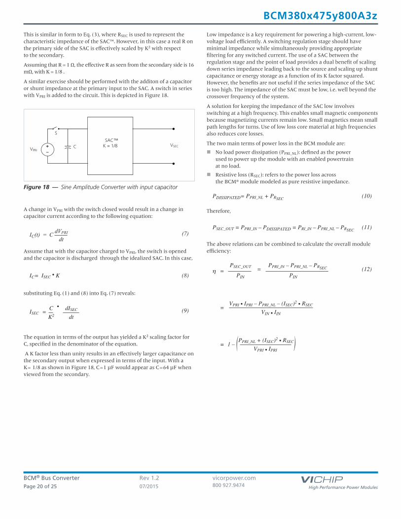
This is similar in form to Eq. (3), where RSEC is used to represent thecharacteristic impedance of the SAC™. However, in this case a real R onthe primary side of the SAC is effectively scaled by K2 with respect to the secondary.
Assuming that R = 1 Ω, the effective R as seen from the secondary side is 16 mΩ, with K = 1/8 .
A similar exercise should be performed with the additon of a capacitoror shunt impedance at the primary input to the SAC. A switch in serieswith VPRI is added to the circuit. This is depicted in Figure 18.
A change in VPRI with the switch closed would result in a change incapacitor current according to the following equation:
IC(t) = CdVPRI (7)dt
Assume that with the capacitor charged to VPRI, the switch is openedand the capacitor is discharged through the idealized SAC. In this case,
IC= ISEC • K (8)
substituting Eq. (1) and (8) into Eq. (7) reveals:
ISEC =C • dISEC (9)K2 dt
The equation in terms of the output has yielded a K2 scaling factor forC, specified in the denominator of the equation.
A K factor less than unity results in an effectively larger capacitance onthe secondary output when expressed in terms of the input. With a K= 1/8 as shown in Figure 18, C=1 μF would appear as C= 64 μF whenviewed from the secondary.
Low impedance is a key requirement for powering a high-current, low-voltage load efficiently. A switching regulation stage should haveminimal impedance while simultaneously providing appropriatefiltering for any switched current. The use of a SAC between theregulation stage and the point of load provides a dual benefit of scalingdown series impedance leading back to the source and scaling up shuntcapacitance or energy storage as a function of its K factor squared.However, the benefits are not useful if the series impedance of the SACis too high. The impedance of the SAC must be low, i.e. well beyond thecrossover frequency of the system.
A solution for keeping the impedance of the SAC low involvesswitching at a high frequency. This enables small magnetic componentsbecause magnetizing currents remain low. Small magnetics mean smallpath lengths for turns. Use of low loss core material at high frequenciesalso reduces core losses.
The two main terms of power loss in the BCM module are:
n No load power dissipation (PPRI_NL): defined as the power used to power up the module with an enabled powertrainat no load.
n Resistive loss (RSEC): refers to the power loss across the BCM® module modeled as pure resistive impedance.
PDISSIPATED= PPRI_NL + PRSEC (10)
Therefore,
PSEC_OUT = PPRI_IN – PDISSIPATED = PRI_IN – PPRI_NL – PRSEC (11)
The above relations can be combined to calculate the overall moduleefficiency:
h =PSEC_OUT =
PPRI_IN – PPRI_NL – PRSEC (12)PIN PIN
=VPRI • IPRI – PPRI_NL – (ISEC)2 • RSEC
VIN • IIN
= 1 – (PPRI_NL + (ISEC)2 • RSEC)VPRI • IPRI
C
S
SACK = 1/32Vin
Vout+–
VPRI
VSECCSAC™
K = 1/8
Figure 18 — Sine Amplitude Converter with input capacitor
S
BCM® Bus Converter Rev 1.2 vicorpower.comPage 20 of 25 07/2015 800 927.9474
BCM380x475y800A3z
BCM® Bus Converter Rev 1.2 vicorpower.comPage 21 of 25 07/2015 800 927.9474
BCM380x475y800A3z
Input and Output Filter Design
A major advantage of SAC™ systems versus conventional PWMconverters is that the transformer based SAC does not require externalfiltering to function properly. The resonant LC tank, operated atextreme high frequency, is amplitude modulated as a function of inputvoltage and output current and efficiently transfers charge through theisolation transformer. A small amount of capacitance embedded in theprimary and secondary stages of the module is sufficient for fullfunctionality and is key to achieving power density.
This paradigm shift requires system design to carefully evaluateexternal filters in order to:
n Guarantee low source impedance:To take full advantage of the BCM module’s dynamic response, the impedance presented to its input terminals must be low from DC to approximately 5 MHz. The connection of the bus converter module to its power source should be implemented with minimal distribution inductance. If the interconnect inductance exceeds 100 nH, the input should be bypassed with a RC damper to retain low source impedance and stable operation. With an interconnect inductance of 200 nH, the RC damper may be as high as 1 μF in series with 0.3 Ω. A single electrolytic or equivalent low-Q capacitor may be used in place of the series RC bypass.
n Further reduce input and/or output voltage ripple without
sacrificing dynamic response:Given the wide bandwidth of the module, the source response is generally the limiting factor in the overall system response. Anomalies in the response of the source will appear at the output of the module multiplied by its K factor.
n Protect the module from overvoltage transients imposed
by the system that would exceed maximum ratings and
induce stresses:The module primary/secondary voltage ranges shall not be exceeded. An internal overvoltage lockout function prevents operation outside of the normal operating input range. Even when disabled, the powertrain is exposed to the applied voltage and power MOSFETs must withstand it.
Total load capacitance at the output of the BCM module shall notexceed the specified maximum. Owing to the wide bandwidth and lowoutput impedance of the module, low-frequency bypass capacitanceand significant energy storage may be more densely and efficientlyprovided by adding capacitance at the input of the module. Atfrequencies <500 kHz the module appears as an impedance of RSEC
between the source and load.
Within this frequency range, capacitance at the input appears aseffective capacitance on the output per the relationship defined in Eq. (13).
CSEC_EXT =CPRI_EXT (13)
K2
This enables a reduction in the size and number of capacitors used in atypical system.
Thermal Considerations
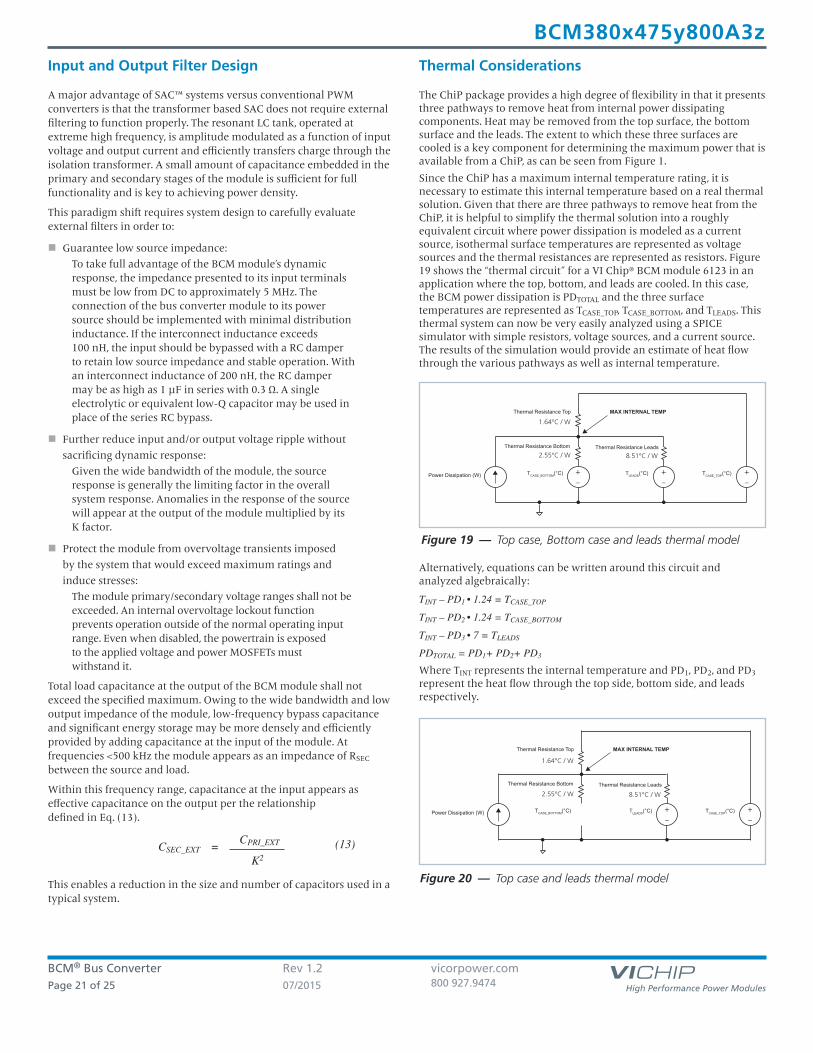
The ChiP package provides a high degree of flexibility in that it presentsthree pathways to remove heat from internal power dissipatingcomponents. Heat may be removed from the top surface, the bottomsurface and the leads. The extent to which these three surfaces arecooled is a key component for determining the maximum power that isavailable from a ChiP, as can be seen from Figure 1.
Since the ChiP has a maximum internal temperature rating, it isnecessary to estimate this internal temperature based on a real thermalsolution. Given that there are three pathways to remove heat from theChiP, it is helpful to simplify the thermal solution into a roughlyequivalent circuit where power dissipation is modeled as a currentsource, isothermal surface temperatures are represented as voltagesources and the thermal resistances are represented as resistors. Figure19 shows the “thermal circuit” for a VI Chip® BCM module 6123 in anapplication where the top, bottom, and leads are cooled. In this case,the BCM power dissipation is PDTOTAL and the three surfacetemperatures are represented as TCASE_TOP, TCASE_BOTTOM, and TLEADS. Thisthermal system can now be very easily analyzed using a SPICEsimulator with simple resistors, voltage sources, and a current source.The results of the simulation would provide an estimate of heat flowthrough the various pathways as well as internal temperature.
Alternatively, equations can be written around this circuit andanalyzed algebraically:
TINT – PD1 • 1.24 = TCASE_TOP
TINT – PD2 • 1.24 = TCASE_BOTTOM
TINT – PD3 • 7 = TLEADS
PDTOTAL = PD1+ PD2+ PD3
Where TINT represents the internal temperature and PD1, PD2, and PD3
represent the heat flow through the top side, bottom side, and leadsrespectively.
+–
+–
+–
MAX INTERNAL TEMP
TCASE_BOTTOM(°C) TLEADS(°C) TCASE_TOP(°C)Power Dissipation (W)
Thermal Resistance Top
Thermal Resistance Bottom Thermal Resistance Leads
+–
+–
MAX INTERNAL TEMP
TCASE_BOTTOM(°C) TLEADS(°C) TCASE_TOP(°C)Power Dissipation (W)
Thermal Resistance Top
Thermal Resistance Bottom Thermal Resistance Leads
Figure 19 — Top case, Bottom case and leads thermal model
Figure 20 — Top case and leads thermal model
1.64 °C / W
2.55 °C / W 8.51 °C / W
1.64 °C / W
2.55 °C / W 8.51 °C / W
BCM® Bus Converter Rev 1.2 vicorpower.comPage 22 of 25 07/2015 800 927.9474
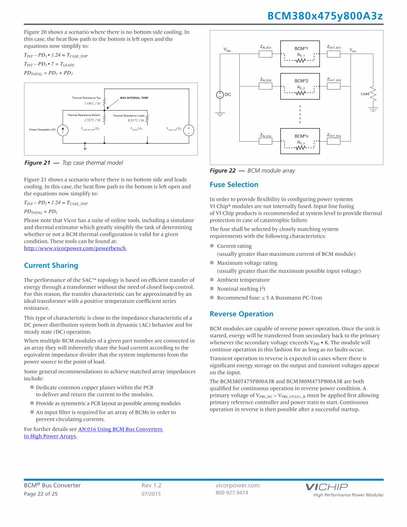
BCM380x475y800A3z Figure 20 shows a scenario where there is no bottom side cooling. Inthis case, the heat flow path to the bottom is left open and theequations now simplify to:
TINT – PD1 • 1.24 = TCASE_TOP
TINT – PD3 • 7 = TLEADS
PDTOTAL = PD1 + PD3
Figure 21 shows a scenario where there is no bottom side and leadscooling. In this case, the heat flow path to the bottom is left open andthe equations now simplify to:
TINT – PD1 • 1.24 = TCASE_TOP
PDTOTAL = PD1
Please note that Vicor has a suite of online tools, including a simulatorand thermal estimator which greatly simplify the task of determiningwhether or not a BCM thermal configuration is valid for a givencondition. These tools can be found at:http://www.vicorpower.com/powerbench.
Current Sharing
The performance of the SAC™ topology is based on efficient transfer ofenergy through a transformer without the need of closed loop control.For this reason, the transfer characteristic can be approximated by anideal transformer with a positive temperature coefficient seriesresistance.
This type of characteristic is close to the impedance characteristic of aDC power distribution system both in dynamic (AC) behavior and forsteady state (DC) operation.
When multiple BCM modules of a given part number are connected inan array they will inherently share the load current according to theequivalent impedance divider that the system implements from thepower source to the point of load.
Some general recommendations to achieve matched array impedancesinclude:
n Dedicate common copper planes within the PCB to deliver and return the current to the modules.
n Provide as symmetric a PCB layout as possible among modules
n An input filter is required for an array of BCMs in order to prevent circulating currents.
For further details see AN:016 Using BCM Bus Converters in High Power Arrays.
Fuse Selection
In order to provide flexibility in configuring power systems VI Chip® modules are not internally fused. Input line fusing of VI Chip products is recommended at system level to provide thermalprotection in case of catastrophic failure.
The fuse shall be selected by closely matching system requirements with the following characteristics:
n Current rating
(usually greater than maximum current of BCM module)
n Maximum voltage rating
(usually greater than the maximum possible input voltage)
n Ambient temperature
n Nominal melting I2t
n Recommend fuse: ≤ 5 A Bussmann PC-Tron
Reverse Operation
BCM modules are capable of reverse power operation. Once the unit isstarted, energy will be transferred from secondary back to the primarywhenever the secondary voltage exceeds VPRI • K. The module willcontinue operation in this fashion for as long as no faults occur.
Transient operation in reverse is expected in cases where there issignificant energy storage on the output and transient voltages appearon the input.
The BCM380T475P800A3R and BCM380M475P800A3R are bothqualified for continuous operation in reverse power condition. Aprimary voltage of VPRI_DC > VPRI_UVLO+_R must be applied first allowingprimary reference controller and power train to start. Continuousoperation in reverse is then possible after a successful startup.
BCM®1R0_1
ZIN_EQ1 ZOUT_EQ1
ZOUT_EQ2
VSEC
ZOUT_EQn
ZIN_EQ2
ZIN_EQn
R0_2
R0_n
BCM®2
BCM®n
LoadDC
VPRI
+
Figure 22 — BCM module array
+–
MAX INTERNAL TEMP
TCASE_BOTTOM(°C) TLEADS(°C) TCASE_TOP(°C)Power Dissipation (W)
Thermal Resistance Top
Thermal Resistance Bottom Thermal Resistance Leads
Figure 21 — Top case thermal model
1.64 °C / W
2.55 °C / W 8.51 °C / W
BCM® Bus Converter Rev 1.2 vicorpower.comPage 23 of 25 07/2015 800 927.9474
BCM380x475y800A3z
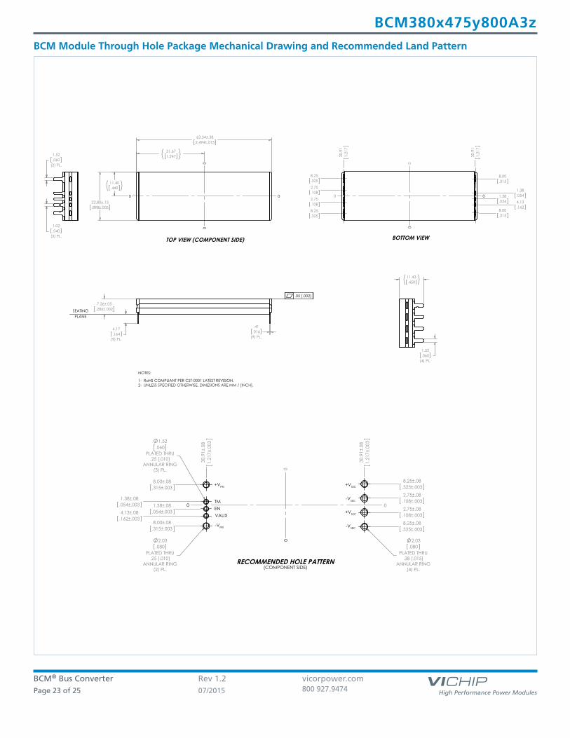
BCM Module Through Hole Package Mechanical Drawing and Recommended Land Pattern
11.40.449
22.80±.13.898±.005
31.671.247
63.34±.382.494±.015
0
0
0
0
TOP VIEW (COMPONENT SIDE)
1.52.060
(2) PL.
1.02.040
(3) PL.
11.43.450
1.52.060
(4) PL.
0
30.9
11.
217
30
.91
1.21
7
0
2.75.108
8.25.325
2.75.108
8.25.325
8.00.315
1.38.054
1.38.054
4.13.162
8.00.315
0
0
BOTTOM VIEW
.41.016
(9) PL.
4.17.164
(9) PL.
7.26±.05.286±.002
SEATING.
PLANE
.05 [.002]
2.03.080
PLATED THRU.25 [.010]
ANNULAR RING(2) PL.
1.52.060
PLATED THRU.25 [.010]
ANNULAR RING(3) PL.
2.03.080
PLATED THRU.38 [.015]
ANNULAR RING(4) PL.
0
2.75±.08.108±.003
8.25±.08.325±.003
2.75±.08.108±.003
8.25±.08.325±.003
8.00±.08.315±.003
4.13±.08.162±.003
1.38±.08.054±.003
1.38±.08.054±.003
8.00±.08.315±.003
0
30.9
1±.0
81.
217±
.003
30
.91±
.08
1.21
7±.0
03
0
0
+VPRI
TM
EN
VAUX
-VPRI
+VSEC
+VSEC
-VSEC
-VSEC
RECOMMENDED HOLE PATTERN(COMPONENT SIDE)
NOTES:
1- RoHS COMPLIANT PER CST-0001 LATEST REVISION.2- UNLESS SPECIFIED OTHERWISE, DIMESIONS ARE MM / [INCH].
BCM® Bus Converter Rev 1.2 vicorpower.comPage 24 of 25 07/2015 800 927.9474
BCM380x475y800A3z
Revision History
Revision Date Description Page Number(s)
1.1 05/15 Previous version of part #BCM380x475y800A30 n/a
1.2 07/21/15 Multiple updates. Additional new products. all Analog HV BCM qualified for continuous reversible operations.

BCM® Bus Converter Rev 1.2 vicorpower.comPage 25 of 25 07/2015 800 927.9474
Vicor’s comprehensive line of power solutions includes high density AC-DC and DC-DC modules andaccessory components, fully configurable AC-DC and DC-DC power supplies, and complete custompower systems.
Information furnished by Vicor is believed to be accurate and reliable. However, no responsibility is assumed by Vicor for its use. Vicor makes norepresentations or warranties with respect to the accuracy or completeness of the contents of this publication. Vicor reserves the right to makechanges to any products, specifications, and product descriptions at any time without notice. Information published by Vicor has been checked andis believed to be accurate at the time it was printed; however, Vicor assumes no responsibility for inaccuracies. Testing and other quality controls areused to the extent Vicor deems necessary to support Vicor’s product warranty. Except where mandated by government requirements, testing of allparameters of each product is not necessarily performed. Specifications are subject to change without notice.
Vicor’s Standard Terms and ConditionsAll sales are subject to Vicor’s Standard Terms and Conditions of Sale, which are available on Vicor’s webpage or upon request.
Product WarrantyIn Vicor’s standard terms and conditions of sale, Vicor warrants that its products are free from non-conformity to its Standard Specifications (the“Express Limited Warranty”). This warranty is extended only to the original Buyer for the period expiring two (2) years after the date of shipmentand is not transferable.UNLESS OTHERWISE EXPRESSLY STATED IN A WRITTEN SALES AGREEMENT SIGNED BY A DULY AUTHORIZED VICOR SIGNATORY, VICOR DISCLAIMSALL REPRESENTATIONS, LIABILITIES, AND WARRANTIES OF ANY KIND (WHETHER ARISING BY IMPLICATION OR BY OPERATION OF LAW) WITHRESPECT TO THE PRODUCTS, INCLUDING, WITHOUT LIMITATION, ANY WARRANTIES OR REPRESENTATIONS AS TO MERCHANTABILITY, FITNESS FORPARTICULAR PURPOSE, INFRINGEMENT OF ANY PATENT, COPYRIGHT, OR OTHER INTELLECTUAL PROPERTY RIGHT, OR ANY OTHER MATTER.
This warranty does not extend to products subjected to misuse, accident, or improper application, maintenance, or storage. Vicor shall not be liablefor collateral or consequential damage. Vicor disclaims any and all liability arising out of the application or use of any product or circuit and assumesno liability for applications assistance or buyer product design. Buyers are responsible for their products and applications using Vicor products andcomponents. Prior to using or distributing any products that include Vicor components, buyers should provide adequate design, testing andoperating safeguards.
Vicor will repair or replace defective products in accordance with its own best judgment. For service under this warranty, the buyer must contactVicor to obtain a Return Material Authorization (RMA) number and shipping instructions. Products returned without prior authorization will bereturned to the buyer. The buyer will pay all charges incurred in returning the product to the factory. Vicor will pay all reshipment charges if theproduct was defective within the terms of this warranty.
Life Support PolicyVICOR’S PRODUCTS ARE NOT AUTHORIZED FOR USE AS CRITICAL COMPONENTS IN LIFE SUPPORT DEVICES OR SYSTEMS WITHOUT THE EXPRESSPRIOR WRITTEN APPROVAL OF THE CHIEF EXECUTIVE OFFICER AND GENERAL COUNSEL OF VICOR CORPORATION. As used herein, life supportdevices or systems are devices which (a) are intended for surgical implant into the body, or (b) support or sustain life and whose failure to performwhen properly used in accordance with instructions for use provided in the labeling can be reasonably expected to result in a significant injury to theuser. A critical component is any component in a life support device or system whose failure to perform can be reasonably expected to cause thefailure of the life support device or system or to affect its safety or effectiveness. Per Vicor Terms and Conditions of Sale, the user of Vicor productsand components in life support applications assumes all risks of such use and indemnifies Vicor against all liability and damages.
Intellectual Property Notice
Vicor and its subsidiaries own Intellectual Property (including issued U.S. and pending patent applications) relating to the products described in thisdata sheet. No license, whether express, implied, or arising by estoppel or otherwise, to any intellectual property rights is granted by this document.Interested parties should contact Vicor's Intellectual Property Department.
The products described on this data sheet are protected by the following U.S. Patents Numbers:6,911,848; 6,930,893; 6,934,166; 7,145,786; 7,782,639; 8,427,269 and for use under 6,975,098 and 6,984,965.
Vicor Corporation25 Frontage Road
Andover, MA, USA 01810Tel: 800-735-6200Fax: 978-475-6715
emailCustomer Service: [email protected]
Technical Support: [email protected]
BCM380x475y800A3z