Embed Size (px)
Citation preview
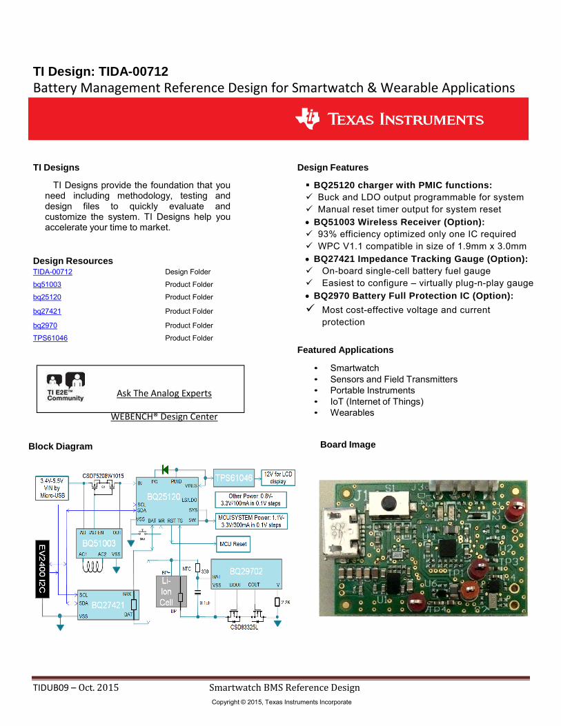
TI Design: TIDA-00712 Battery Management Reference Design for Smartwatch & Wearable Applications
TI Designs
TI Designs provide the foundation that you need including methodology, testing and design files to quickly evaluate and customize the system. TI Designs help you accelerate your time to market.
Design Resources TIDA-00712 Design Folder
bq51003 Product Folder
bq25120 Product Folder
bq27421 Product Folder
bq2970 Product Folder
TPS61046 Product Folder
Ask The Analog Experts
WEBENCH® Design Center Block Diagram
Design Features
BQ25120 charger with PMIC functions: Buck and LDO output programmable for system Manual reset timer output for system reset BQ51003 Wireless Receiver (Option): 93% efficiency optimized only one IC required WPC V1.1 compatible in size of 1.9mm x 3.0mm BQ27421 Impedance Tracking Gauge (Option): On-board single-cell battery fuel gauge Easiest to configure – virtually plug-n-play gauge BQ2970 Battery Full Protection IC (Option):
Most cost-effective voltage and current protection
Featured Applications
• Smartwatch • Sensors and Field Transmitters • Portable Instruments • IoT (Internet of Things) • Wearables
Board Image
TIDUB09 – Oct.2015 SmartwatchBMSReferenceDesign
Copyright © 2015, Texas Instruments Incorporate
www.ti.com
TIDUB09 – Oct.2015 Smartwatch BMS Reference Design2
Copyright © 2015, Texas Instruments Incorporated
1. System Description
The TI design TIDA-00712 is a reference design for Smartwatch BMS (Battery Management Solution); It’s suitable
for low power wearable devices like smartwatch applications. The design includes following devices:
• bq25120, it’s an ultra-low current 1 cell Li-ion linear charger;
• bq51003, it’s a highly integrated Qi-compliant wireless power receiver;
• bq2970, it’s a cost-effective voltage and current protection Integrated Circuit;
• bq27421, it’s a system-side(tm) with integrated sense resistor battery fuel gauge;
• TPS61046, it’s a booster with output up to 28V for LCD kinds of display devices.
The design is implemented in a small size (20mm x 29mm) PCB; its input power can be from a Micro-USB
connector or Qi-compliant wireless power transmitter; the selection of 2 input power sources is automatically, wireless
power will be turned off whenever 5V power supply from Micro-USB connector is detected.
The design gives capability of options for customers’ specified application choice; following functions can be
bypassed by a 0-Ohm resistor: wireless power; gas gauging and protection.
The design can support charging currents from 5 mA to 300 mA; its configurable termination current can be down to
0.5mA. The included schematic is designed for 260mA charge current and 8 mA termination current by external resistor,
but can be overwrote by I2C configuration.
www.ti.com
TIDUB09 – Oct.2015 Smartwatch BMS Reference Design3
Copyright © 2015, Texas Instruments Incorporated
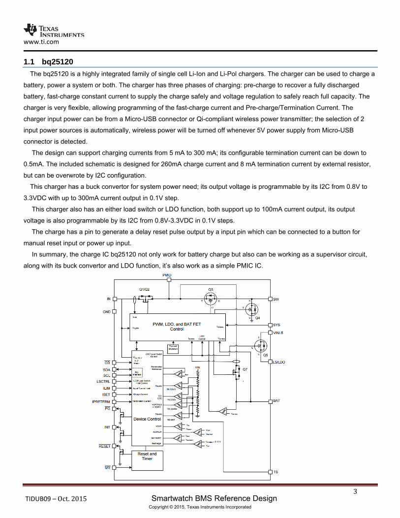
1.1 bq25120
The bq25120 is a highly integrated family of single cell Li-Ion and Li-Pol chargers. The charger can be used to charge a
battery, power a system or both. The charger has three phases of charging: pre-charge to recover a fully discharged
battery, fast-charge constant current to supply the charge safely and voltage regulation to safely reach full capacity. The
charger is very flexible, allowing programming of the fast-charge current and Pre-charge/Termination Current. The
charger input power can be from a Micro-USB connector or Qi-compliant wireless power transmitter; the selection of 2
input power sources is automatically, wireless power will be turned off whenever 5V power supply from Micro-USB
connector is detected.
The design can support charging currents from 5 mA to 300 mA; its configurable termination current can be down to
0.5mA. The included schematic is designed for 260mA charge current and 8 mA termination current by external resistor,
but can be overwrote by I2C configuration.
This charger has a buck convertor for system power need; its output voltage is programmable by its I2C from 0.8V to
3.3VDC with up to 300mA current output in 0.1V step.
This charger also has an either load switch or LDO function, both support up to 100mA current output, its output
voltage is also programmable by its I2C from 0.8V-3.3VDC in 0.1V steps.
The charge has a pin to generate a delay reset pulse output by a input pin which can be connected to a button for
manual reset input or power up input.
In summary, the charge IC bq25120 not only work for battery charge but also can be working as a supervisor circuit,
along with its buck convertor and LDO function, it’s also work as a simple PMIC IC.
www.ti.com
TIDUB09 – Oct.2015 Smartwatch BMS Reference Design4
Copyright © 2015, Texas Instruments Incorporated
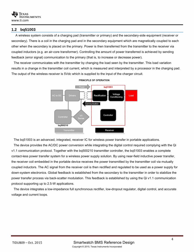
1.2 bq51003
A wireless system consists of a charging pad (transmitter or primary) and the secondary-side equipment (receiver or
secondary). There is a coil in the charging pad and in the secondary equipment which are magnetically coupled to each
other when the secondary is placed on the primary. Power is then transferred from the transmitter to the receiver via
coupled inductors (e.g. an air-core transformer). Controlling the amount of power transferred is achieved by sending
feedback (error signal) communication to the primary (that is, to increase or decrease power).
The receiver communicates with the transmitter by changing the load seen by the transmitter. This load variation
results in a change in the transmitter coil current, which is measured and interpreted by a processor in the charging pad.
The output of the wireless receiver is 5Vdc which is supplied to the input of the charger circuit.
The bq51003 is an advanced, integrated, receiver IC for wireless power transfer in portable applications.
The device provides the AC/DC power conversion while integrating the digital control required complying with the Qi
v1.1 communication protocol. Together with the bq500210 transmitter controller, the bq51003 enables a complete
contact-less power transfer system for a wireless power supply solution. By using near-field inductive power transfer,
the receiver coil embedded in the portable device receives the power transmitted by the transmitter coil via mutually
coupled inductors. The AC signal from the receiver coil is then rectified and regulated to be used as a power supply for
down-system electronics. Global feedback is established from the secondary to the transmitter in order to stabilize the
power transfer process via back-scatter modulation. This feedback is established by using the Qi v1.1 communication
protocol supporting up to 2.5-W applications.
The device integrates a low-impedance full synchronous rectifier, low-dropout regulator, digital control, and accurate
voltage and current loops.
www.ti.com
TIDUB09 – Oct.2015 Smartwatch BMS Reference Design5
Copyright © 2015, Texas Instruments Incorporated
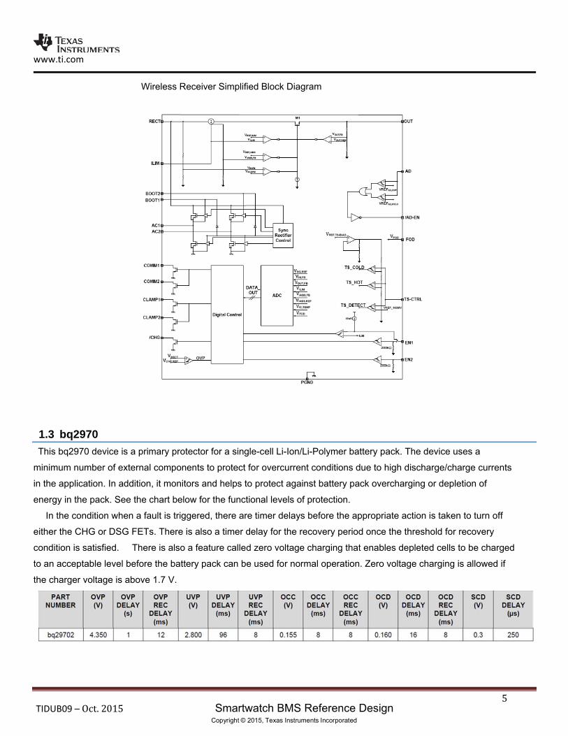
Wireless Receiver Simplified Block Diagram
1.3 bq2970
This bq2970 device is a primary protector for a single-cell Li-Ion/Li-Polymer battery pack. The device uses a
minimum number of external components to protect for overcurrent conditions due to high discharge/charge currents
in the application. In addition, it monitors and helps to protect against battery pack overcharging or depletion of
energy in the pack. See the chart below for the functional levels of protection.
In the condition when a fault is triggered, there are timer delays before the appropriate action is taken to turn off
either the CHG or DSG FETs. There is also a timer delay for the recovery period once the threshold for recovery
condition is satisfied. There is also a feature called zero voltage charging that enables depleted cells to be charged
to an acceptable level before the battery pack can be used for normal operation. Zero voltage charging is allowed if
the charger voltage is above 1.7 V.
www.ti.com
TIDUB09 – Oct.2015 Smartwatch BMS Reference Design6
Copyright © 2015, Texas Instruments Incorporated
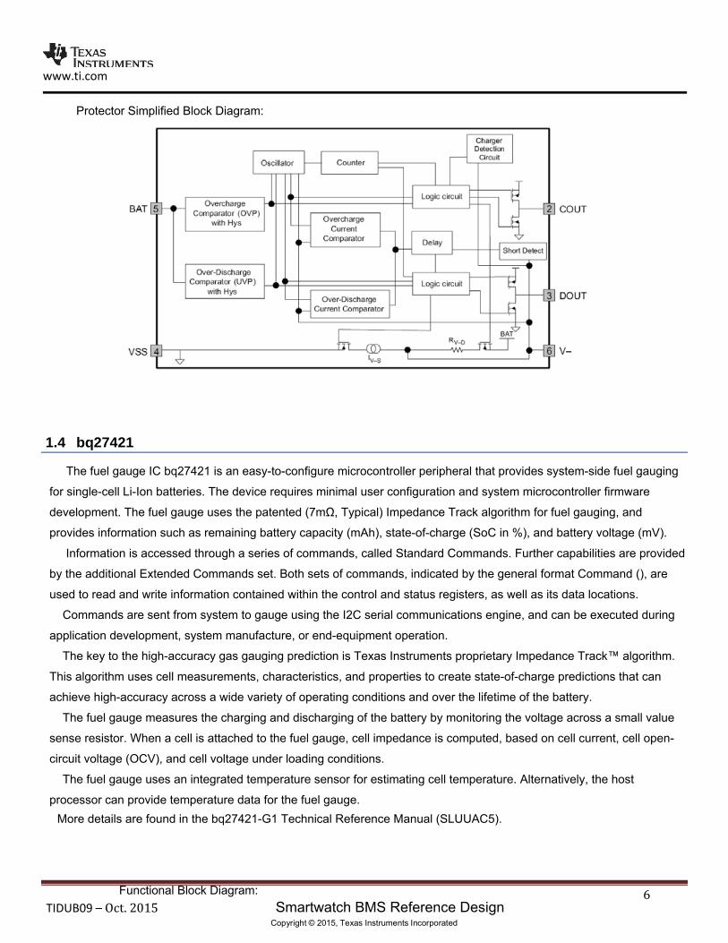
Protector Simplified Block Diagram:
1.4 bq27421
The fuel gauge IC bq27421 is an easy-to-configure microcontroller peripheral that provides system-side fuel gauging
for single-cell Li-Ion batteries. The device requires minimal user configuration and system microcontroller firmware
development. The fuel gauge uses the patented (7mΩ, Typical) Impedance Track algorithm for fuel gauging, and
provides information such as remaining battery capacity (mAh), state-of-charge (SoC in %), and battery voltage (mV).
Information is accessed through a series of commands, called Standard Commands. Further capabilities are provided
by the additional Extended Commands set. Both sets of commands, indicated by the general format Command (), are
used to read and write information contained within the control and status registers, as well as its data locations.
Commands are sent from system to gauge using the I2C serial communications engine, and can be executed during
application development, system manufacture, or end-equipment operation.
The key to the high-accuracy gas gauging prediction is Texas Instruments proprietary Impedance Track™ algorithm.
This algorithm uses cell measurements, characteristics, and properties to create state-of-charge predictions that can
achieve high-accuracy across a wide variety of operating conditions and over the lifetime of the battery.
The fuel gauge measures the charging and discharging of the battery by monitoring the voltage across a small value
sense resistor. When a cell is attached to the fuel gauge, cell impedance is computed, based on cell current, cell open-
circuit voltage (OCV), and cell voltage under loading conditions.
The fuel gauge uses an integrated temperature sensor for estimating cell temperature. Alternatively, the host
processor can provide temperature data for the fuel gauge.
More details are found in the bq27421-G1 Technical Reference Manual (SLUUAC5).
Functional Block Diagram:
www.ti.com
TIDUB09 – Oct.2015 Smartwatch BMS Reference Design7
Copyright © 2015, Texas Instruments Incorporated
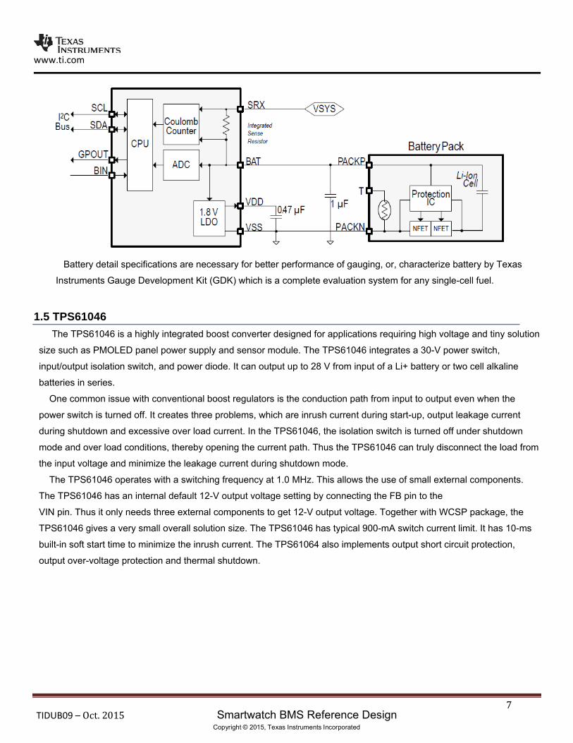
Battery detail specifications are necessary for better performance of gauging, or, characterize battery by Texas
Instruments Gauge Development Kit (GDK) which is a complete evaluation system for any single-cell fuel.
1.5 TPS61046
The TPS61046 is a highly integrated boost converter designed for applications requiring high voltage and tiny solution
size such as PMOLED panel power supply and sensor module. The TPS61046 integrates a 30-V power switch,
input/output isolation switch, and power diode. It can output up to 28 V from input of a Li+ battery or two cell alkaline
batteries in series.
One common issue with conventional boost regulators is the conduction path from input to output even when the
power switch is turned off. It creates three problems, which are inrush current during start-up, output leakage current
during shutdown and excessive over load current. In the TPS61046, the isolation switch is turned off under shutdown
mode and over load conditions, thereby opening the current path. Thus the TPS61046 can truly disconnect the load from
the input voltage and minimize the leakage current during shutdown mode.
The TPS61046 operates with a switching frequency at 1.0 MHz. This allows the use of small external components.
The TPS61046 has an internal default 12-V output voltage setting by connecting the FB pin to the
VIN pin. Thus it only needs three external components to get 12-V output voltage. Together with WCSP package, the
TPS61046 gives a very small overall solution size. The TPS61046 has typical 900-mA switch current limit. It has 10-ms
built-in soft start time to minimize the inrush current. The TPS61064 also implements output short circuit protection,
output over-voltage protection and thermal shutdown.
www.ti.com
TIDUB09 – Oct.2015 Smartwatch BMS Reference Design8
Copyright © 2015, Texas Instruments Incorporated
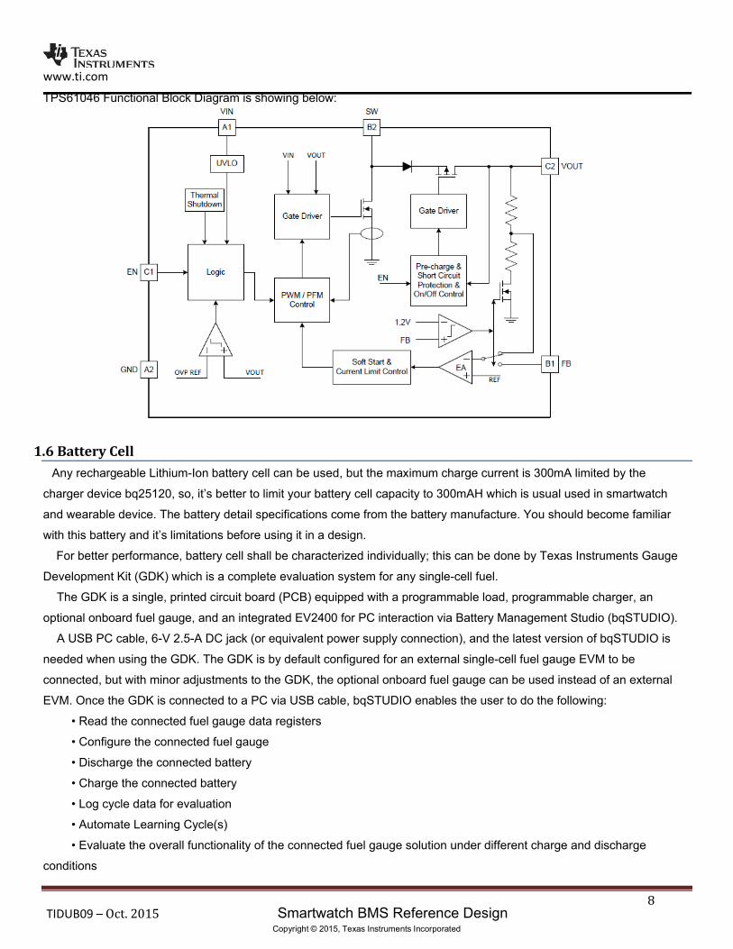
TPS61046 Functional Block Diagram is showing below:
1.6BatteryCell
Any rechargeable Lithium-Ion battery cell can be used, but the maximum charge current is 300mA limited by the
charger device bq25120, so, it’s better to limit your battery cell capacity to 300mAH which is usual used in smartwatch
and wearable device. The battery detail specifications come from the battery manufacture. You should become familiar
with this battery and it’s limitations before using it in a design.
For better performance, battery cell shall be characterized individually; this can be done by Texas Instruments Gauge
Development Kit (GDK) which is a complete evaluation system for any single-cell fuel.
The GDK is a single, printed circuit board (PCB) equipped with a programmable load, programmable charger, an
optional onboard fuel gauge, and an integrated EV2400 for PC interaction via Battery Management Studio (bqSTUDIO).
A USB PC cable, 6-V 2.5-A DC jack (or equivalent power supply connection), and the latest version of bqSTUDIO is
needed when using the GDK. The GDK is by default configured for an external single-cell fuel gauge EVM to be
connected, but with minor adjustments to the GDK, the optional onboard fuel gauge can be used instead of an external
EVM. Once the GDK is connected to a PC via USB cable, bqSTUDIO enables the user to do the following:
• Read the connected fuel gauge data registers
• Configure the connected fuel gauge
• Discharge the connected battery
• Charge the connected battery
• Log cycle data for evaluation
• Automate Learning Cycle(s)
• Evaluate the overall functionality of the connected fuel gauge solution under different charge and discharge
conditions
www.ti.com
TIDUB09 – Oct.2015SmartwatchBMSReferenceDesign
9
Copyright © 2015, Texas Instruments Incorporated
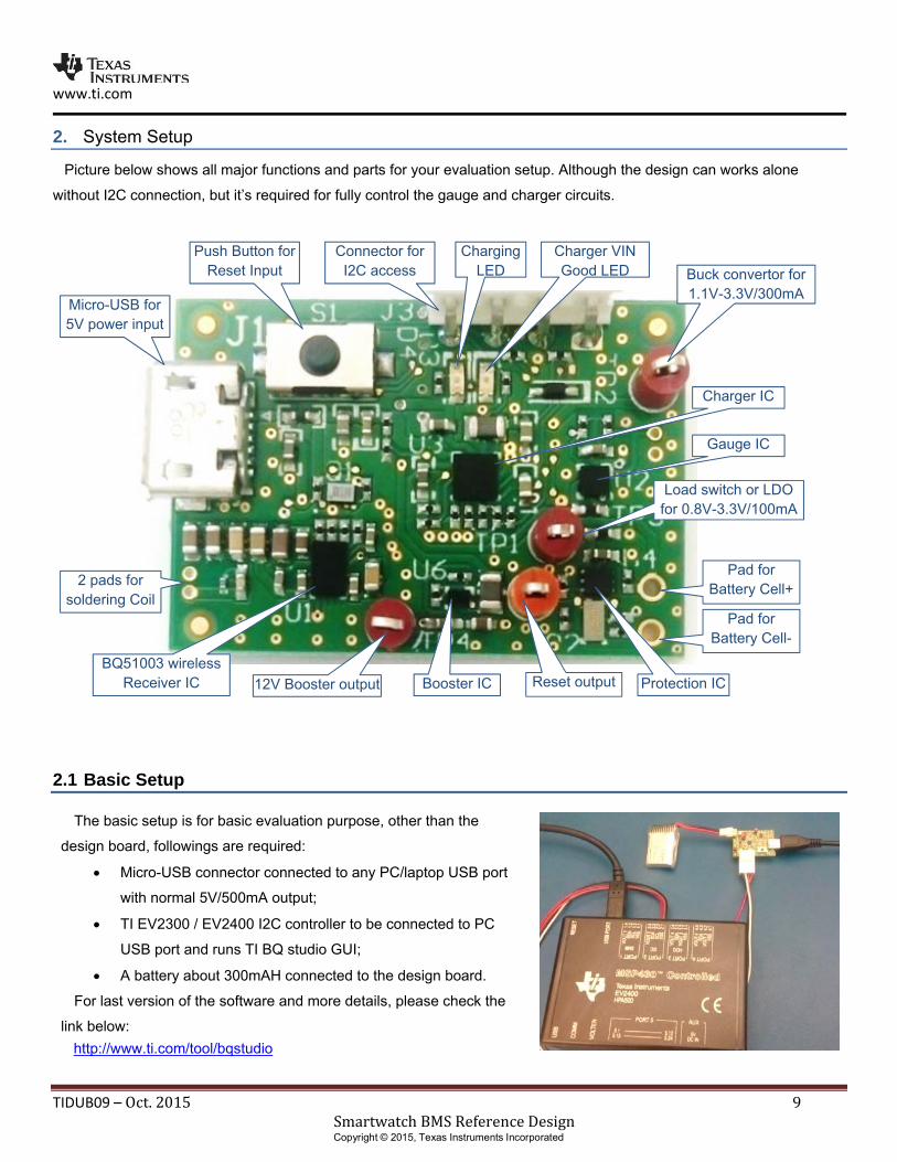
Micro-USB for 5V power input
Push Button for Reset Input
Connector for I2C access Buck convertor for
1.1V-3.3V/300mA
Load switch or LDO for 0.8V-3.3V/100mA
Reset output 12V Booster output
BQ51003 wireless Receiver IC
2 pads for soldering Coil
Pad for Battery Cell+
Booster IC Protection IC
Gauge IC
Charger IC
Charging LED
Charger VIN Good LED
Pad for Battery Cell-
2. System Setup
Picture below shows all major functions and parts for your evaluation setup. Although the design can works alone
without I2C connection, but it’s required for fully control the gauge and charger circuits.
2.1 Basic Setup
The basic setup is for basic evaluation purpose, other than the
design board, followings are required:
Micro-USB connector connected to any PC/laptop USB port
with normal 5V/500mA output;
TI EV2300 / EV2400 I2C controller to be connected to PC
USB port and runs TI BQ studio GUI;
A battery about 300mAH connected to the design board.
For last version of the software and more details, please check the
link below:
http://www.ti.com/tool/bqstudio
www.ti.com
TIDUB09 – Oct.2015SmartwatchBMSReferenceDesign
10
Copyright © 2015, Texas Instruments Incorporated
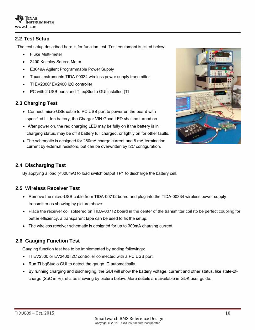
2.2 Test Setup
The test setup described here is for function test. Test equipment is listed below:
Fluke Multi-meter
2400 Keithley Source Meter
E3649A Agilent Programmable Power Supply
Texas Instruments TIDA-00334 wireless power supply transmitter
TI EV2300/ EV2400 I2C controller
PC with 2 USB ports and TI bqStudio GUI installed (TI
2.3 Charging Test
Connect micro-USB cable to PC USB port to power on the board with
specified Li_Ion battery, the Charger VIN Good LED shall be turned on.
After power on, the red charging LED may be fully on if the battery is in
charging status, may be off if battery full charged, or lightly on for other faults.
The schematic is designed for 260mA charge current and 8 mA termination current by external resistors, but can be overwritten by I2C configuration.
2.4 Discharging Test
By applying a load (<300mA) to load switch output TP1 to discharge the battery cell.
2.5 Wireless Receiver Test
Remove the micro-USB cable from TIDA-00712 board and plug into the TIDA-00334 wireless power supply
transmitter as showing by picture above.
Place the receiver coil soldered on TIDA-00712 board in the center of the transmitter coil (to be perfect coupling for
better efficiency, a transparent tape can be used to fix the setup.
The wireless receiver schematic is designed for up to 300mA charging current.
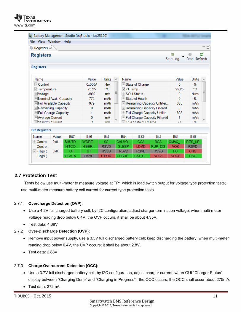
2.6 Gauging Function Test
Gauging function test has to be implemented by adding followings:
TI EV2300 or EV2400 I2C controller connected with a PC USB port.
Run TI bqStudio GUI to detect the gauge IC automatically.
By running charging and discharging, the GUI will show the battery voltage, current and other status, like state-of-
charge (SoC in %), etc. as showing by picture below. More details are available in GDK user guide.
www.ti.com
TIDUB09 – Oct.2015SmartwatchBMSReferenceDesign
11
Copyright © 2015, Texas Instruments Incorporated
2.7 Protection Test
Tests below use multi-meter to measure voltage at TP1 which is load switch output for voltage type protection tests;
use multi-meter measure battery cell current for current type protection tests.
2.7.1 Overcharge Detection (OVP):
Use a 4.2V full charged battery cell, by I2C configuration, adjust charger termination voltage, when multi-meter
voltage reading drop below 0.4V, the OVP occurs, it shall be about 4.35V.
Test data: 4.38V
2.7.2 Over-Discharge Detection (UVP):
Remove input power supply, use a 3.5V full discharged battery cell; keep discharging the battery, when multi-meter
reading drop below 0.4V, the UVP occurs; it shall be about 2.8V.
Test data: 2.88V
2.7.3 Charge Overcurrent Detection (OCC):
Use a 3.7V full discharged battery cell, by I2C configuration, adjust charger current, when GUI “Charger Status”
display between “Charging Done” and “Charging in Progress”, the OCC occurs; the OCC shall occur about 275mA.
Test data: 272mA
www.ti.com
TIDUB09 – Oct.2015SmartwatchBMSReferenceDesign
12
Copyright © 2015, Texas Instruments Incorporated
2.7.4 Discharge Overcurrent Detection (OCD):
Remove input power supply, use a 4.2V battery cell; discharging the battery by 2400 Keithley Source Meter, add
discharge current from 275mA, when multi-meter current reading drop below 1mA, the OCD occurs; the OCD shall
be about 290mA.
Test data: 285mA
2.7.5 Load Short-Circuit Detection (SCP):
Short the load switch output TP1 to ground; the multi-meter current reading shall be less than 1mA which shows
SCP occurs.
Test data: Pass.
2.8 Booster Test
No load voltage output: Use multi-meter measures the booster output at TP4 test loop which shall be 12V
(+/-5%);
Test data: 12.07V.
Loaded voltage output: Apply 25mA load to the booster output at TP4, the output shall be still in the range
of 12V (+/-5%);
Test data: 11.56V
www.ti.com
TIDUB09 – Oct.2015SmartwatchBMSReferenceDesign
13
Copyright © 2015, Texas Instruments Incorporated
3. Charger Test Data in Plots
The test data showing by plots is followings:
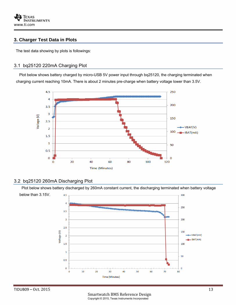
3.1 bq25120 220mA Charging Plot
Plot below shows battery charged by micro-USB 5V power input through bq25120, the charging terminated when
charging current reaching 10mA. There is about 2 minutes pre-charge when battery voltage lower than 3.5V.
3.2 bq25120 260mA Discharging Plot
Plot below shows battery discharged by 260mA constant current, the discharging terminated when battery voltage
below than 3.15V.
www.ti.com
TIDUB09 – Oct.2015SmartwatchBMSReferenceDesign
14
Copyright © 2015, Texas Instruments Incorporated
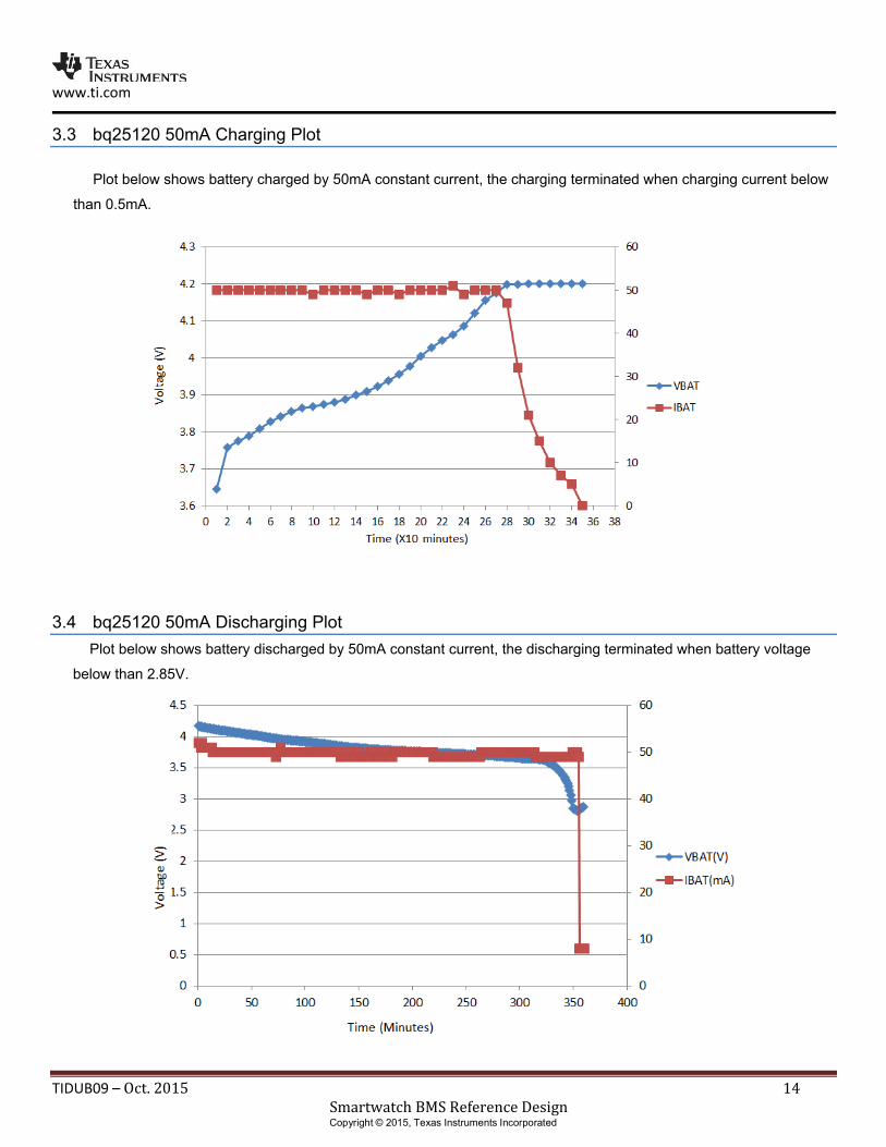
3.3 bq25120 50mA Charging Plot
Plot below shows battery charged by 50mA constant current, the charging terminated when charging current below
than 0.5mA.
3.4 bq25120 50mA Discharging Plot
Plot below shows battery discharged by 50mA constant current, the discharging terminated when battery voltage
below than 2.85V.
www.ti.com
TIDUB09 – Oct.2015SmartwatchBMSReferenceDesign
15
Copyright © 2015, Texas Instruments Incorporated
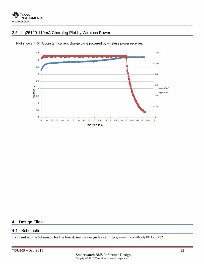
3.5 bq25120 110mA Charging Plot by Wireless Power
Plot shows 110mA constant current charge cycle powered by wireless power receiver.
4 Design Files
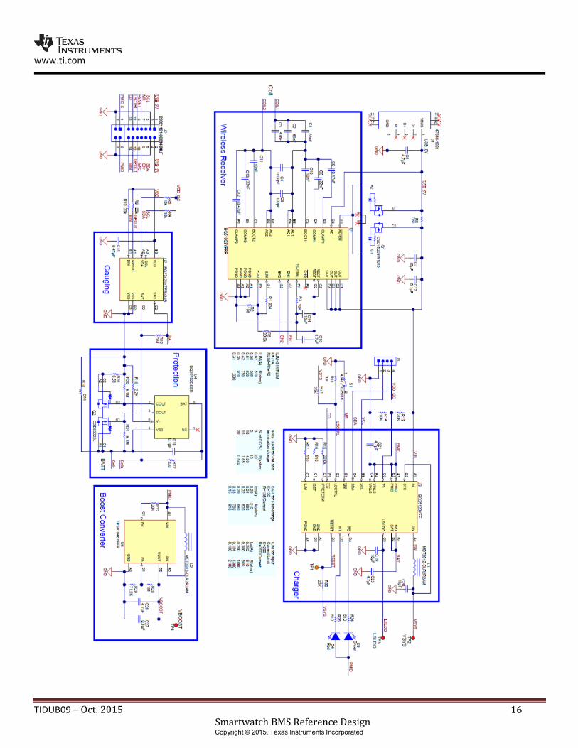
4.1 Schematic
To download the Schematic for the board, see the design files at http://www.ti.com/tool/TIDA‐00712
www.ti.com
TIDUB09 – Oct.2015SmartwatchBMSReferenceDesign
16
Copyright © 2015, Texas Instruments Incorporated
www.ti.com
TIDUB09 – Oct.2015SmartwatchBMSReferenceDesign
17
Copyright © 2015, Texas Instruments Incorporated
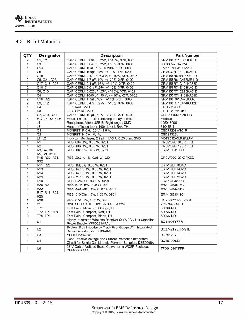
4.2 Bill of Materials
QTY Designator Description Part Number 2 C1, C2 CAP, CERM, 0.068uF, 25V, +/-10%, X7R, 0603 GRM188R71E683KA01D 1 C3 CAP, CERM, 0.047uF, 25V, +/-5%, X7R, 0603 06033C473JAT2A 1 C14 CAP, CERM, 10uF, 16V, +/-20%, X5R, 0603 EMK107BBJ106MA-T 1 C5 CAP, CERM, 100pF, 25V, +/-10%, X7R, 0201 GRM033R71E101KA01D 1 C15 CAP, CERM, 0.47 µF, 6.3 V, +/- 10%, X5R, 0402 GRM155R60J474KE19D 2 C6, C21, C23 CAP, CERM, 4.7 µF, 10V, +/- 20%, X5R, 0402 GRM155R61C475ME11D 1 C17, C18, C27 CAP, CERM, 0.1 µF, 16 V, +/- 10%, X7R, 0402 GRM155R71C104KA88D 2 C10, C11 CAP, CERM, 0.01uF, 25V, +/-10%, X7R, 0402 GRM155R71E103KA01D 2 C8, C13 CAP, CERM, 0.022uF, 25V, +/-10%, X7R, 0402 GRM155R71E223KA61D 1 C4 CAP, CERM, 1800 pF, 50 V, +/- 10%, X7R, 0402 GRM155R71H182KA01D 2 C16, C26 CAP, CERM, 4.7uF, 16V, +/-10%, X5R, 0603 GRM188R61C475KAAJ 2 C9, C12 CAP, CERM, 0.47uF, 25V, +/-10%, X7R, 0603 GRM188R71E474KA12D 1 D4 LED, Red, SMD LTST-C190CKT 1 D3 LED, Green, SMD LTST-C191KGKT 3 C7, C19, C20 CAP, CERM, 10 µF, 10 V, +/- 20%, X5R, 0402 CL05A106MP5NUNC 3 FID1, FID2, FID3 Fiducial mark. There is nothing to buy or mount. Fiducial 1 J1 Receptacle, Micro-USB-B, Right Angle, SMD 1050170001 1 J3 Header (friction lock), 100mil, 4x1, R/A, TH 640457-4 1 Q1 MOSFET, P-CH, -20 V, -1.6 A, CSD75208W1015 1 Q2 MOSFET, N-CH, V, A, CSD83325L 2 L1, L2 Inductor, Multilayer, 2.2 µH, 1.35 A, 0.23 ohm, SMD MDT2012-CLR2R2AM 1 R1 RES, 804, 1%, 0.05 W, 0201 CRCW0201845RFKED 1 R2 RES, 196, 1%, 0.05 W, 0201 CRCW0201196RFKED 1 R3, R4, R6 RES, 10k, 5%, 0.05 W, 0201 ERJ-1GEJ103C
7 R5, R9, R10, R15, R30, R31, R32
RES, 20.0 k, 1%, 0.05 W, 0201 CRCW020120K0FKED
1 R11, R28 RES, 1M, 5%, 0.05 W, 0201 ERJ-1GEF1004C 1 R13 RES, 14.0K, 1%, 0.05 W, 0201 ERJ-1GEF1402C 1 R14 RES, 14.3K, 1%, 0.05 W, 0201 ERJ-1GEF1432C 1 R29 RES, 71.5K, 1%, 0.05 W, 0201 ERJ-1GEF7152C 1 R19 RES, 2.2K, 1%, 0.05 W, 0201 ERJ-1GEJ222C 2 R20, R21 RES, 5.1M, 5%, 0.05 W, 0201 ERJ-1GEJ515C 1 R22 RES, 330 Ohm, 5%, 0.05 W, 0201 ERJ-1GEJ331C
4 R17, R16, R24, R25
RES, 510 Ohm, 5%, 0.05 W, 0201 ERJ-1GEJ511C
1 R26 RES, 0.56, 5%, 0.05 W, 0201 UCR006YVPFLR560 1 S1 SWITCH TACTILE SPST-NO 0.05A 32V 732-7045-1-ND 1 TP1 Test Point, Miniature, Orange, TH 5003K-ND 3 TP2, TP3, TP4 Test Point, Compact, Red, TH 5005K-ND 0 TP5, TP6 Test Point, Compact, Black, TH 5006K-ND
1 U1 Highly Integrated Wireless Receiver Qi (WPC v1.1) Compliant Power Supply, YFP0028APAL
BQ51003YFPR
1 U2 System-Side Impedance Track Fuel Gauge With Integrated Sense Resistor, YZF0009AKAL
BQ27421YZFR-G1B
1 U3 YFF0025AWAW BQ25120YFP
1 U4 Cost-Effective Voltage and Current Protection Integrated Circuit for Single-Cell Li-Ion/Li-Polymer Batteries, DSE0006A
BQ2970DSER
1 U6 28-V Output Voltage Boost Converter in WCSP Package, YFF0006AAAA
TPS61046YFFR
www.ti.com
TIDUB09 – Oct.2015SmartwatchBMSReferenceDesign
18
Copyright © 2015, Texas Instruments Incorporated
4.3 PCB Layout Recommendations
Layout Guidelines As for all switching power supplies, the PCB layout is an important step in the design, especially at high peak
currents and high switching frequencies. If the layout is not carefully done, the boost charger and buck converter
could show stability problems as well as EMI problems. Therefore, use wide and short traces for the main current path
and for the power ground paths. The input and output capacitors as well as the inductors should be placed as close
as possible to the IC. For the boost charger the first priority is the output capacitors, including the 0.1uF bypass
capacitor (CBYP). Next the input capacitor should be placed as close as possible between VIN and VSS. Last in
priority is the boost charger's
inductor, which should be placed close to LBOOST and VIN. For the buck converter, the output capacitor COUT should
be placed as close as possible between VOUT and VSS. The buck converter inductor (L2) should be placed as close
as possible between the switching node LBUCK and VOUT. It is best to use vias and bottom traces for connecting the
inductors to their respective pins instead of the capacitors.
To minimize noise pickup by the high impedance voltage setting nodes the external resistors should be placed so that
the traces connecting the midpoints of each divider to their respective pins are as short as possible. When laying out
the non-power ground return paths (for example, from resistors and CREF), it is recommended to use short traces as
well, separated from the power ground traces and connected to VSS. This avoids ground shift problems, which can
occur due to superimposition of power ground current and control ground current. The PowerPAD should not be used
as a power ground return path.
The remaining pins are either NC pins that should be connected to the PowerPAD as shown below or digital signals
with minimal layout restrictions.
During board assembly, contaminants such as solder flux and even some board cleaning agents can leave residue
that may form parasitic resistors across the physical resistors/capacitors and/or from one end of a resistor/capacitor to
ground, especially in humid, fast airflow environments. This can result in the voltage regulation and threshold levels
changing significantly from those expected per the installed components. Therefore, it is highly recommended that no
ground planes be poured near the voltage setting resistors or the sample and hold capacitor. In addition, the boards
must be carefully cleaned, possibly rotated at least once during cleaning, and then rinsed with de-ionized water until
the ionic contamination of that water is well above 50mOhm. If this is not feasible, then it is recommended that the sum
of the voltage setting resistors be reduced to at least 5X below the measured ionic contamination.
www.ti.com
TIDUB09 – Oct.2015SmartwatchBMSReferenceDesign
19
Copyright © 2015, Texas Instruments Incorporated
Thermal Considerations
Implementation of integrated circuits in low-profile and fine-pitch surface-mount packages typically requires special
attention to power dissipation. Many system-dependent issues such as thermal coupling, airflow, added heat sinks
and convection surfaces, and the presence of other heat-generating components affect the power dissipation limits of
a given component.
Three basic approaches for enhancing thermal performance are listed below.
• Improving the power-dissipation capability of the PCB design
• Improving the thermal coupling of the component to the PCB
• Introducing airflow in the system
For more details on how to use the thermal parameters in the dissipation ratings table please check the Thermal
Characteristics Application Note (SZZA017) and the IC Package Thermal Metrics Application Note (SPRA953).
TIDUB09 – Oct.2015SmartwatchBMSReferenceDesign
24
Copyright © 2015, Texas Instruments Incorporated
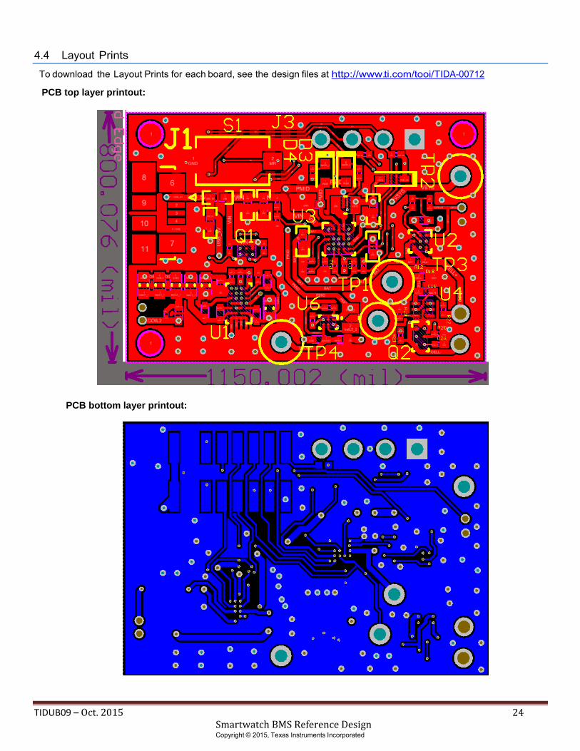
4.4 Layout Prints
To download the Layout Prints for each board, see the design files at http://www.ti.com/tooi/TIDA-00712
PCB top layer printout:
PCB bottom layer printout:
TIDUB09 – Oct.2015SmartwatchBMSReferenceDesign
25
Copyright © 2015, Texas Instruments Incorporated
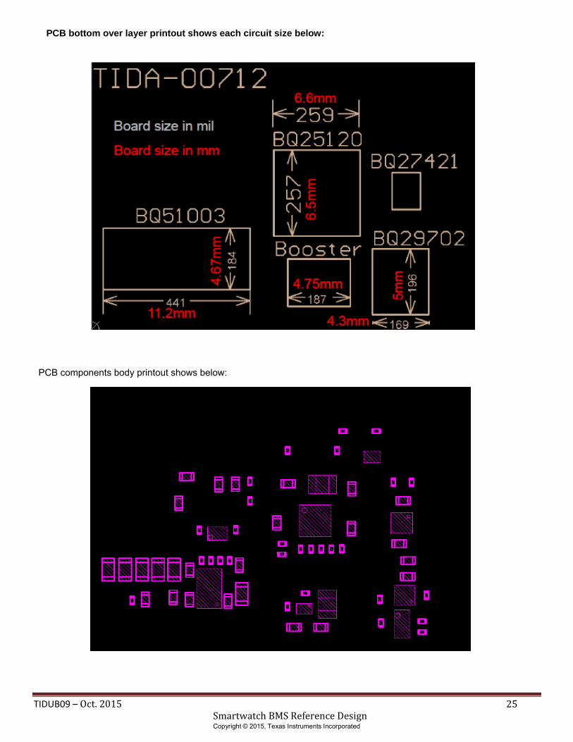
PCB bottom over layer printout shows each circuit size below: PCB components body printout shows below:

IMPORTANT NOTICE FOR TI REFERENCE DESIGNS
Texas Instruments Incorporated ("TI") reference designs are solely intended to assist designers (“Buyers”) who are developing systems thatincorporate TI semiconductor products (also referred to herein as “components”). Buyer understands and agrees that Buyer remainsresponsible for using its independent analysis, evaluation and judgment in designing Buyer’s systems and products.TI reference designs have been created using standard laboratory conditions and engineering practices. TI has not conducted anytesting other than that specifically described in the published documentation for a particular reference design. TI may makecorrections, enhancements, improvements and other changes to its reference designs.Buyers are authorized to use TI reference designs with the TI component(s) identified in each particular reference design and to modify thereference design in the development of their end products. HOWEVER, NO OTHER LICENSE, EXPRESS OR IMPLIED, BY ESTOPPELOR OTHERWISE TO ANY OTHER TI INTELLECTUAL PROPERTY RIGHT, AND NO LICENSE TO ANY THIRD PARTY TECHNOLOGYOR INTELLECTUAL PROPERTY RIGHT, IS GRANTED HEREIN, including but not limited to any patent right, copyright, mask work right,or other intellectual property right relating to any combination, machine, or process in which TI components or services are used.Information published by TI regarding third-party products or services does not constitute a license to use such products or services, or awarranty or endorsement thereof. Use of such information may require a license from a third party under the patents or other intellectualproperty of the third party, or a license from TI under the patents or other intellectual property of TI.TI REFERENCE DESIGNS ARE PROVIDED "AS IS". TI MAKES NO WARRANTIES OR REPRESENTATIONS WITH REGARD TO THEREFERENCE DESIGNS OR USE OF THE REFERENCE DESIGNS, EXPRESS, IMPLIED OR STATUTORY, INCLUDING ACCURACY ORCOMPLETENESS. TI DISCLAIMS ANY WARRANTY OF TITLE AND ANY IMPLIED WARRANTIES OF MERCHANTABILITY, FITNESSFOR A PARTICULAR PURPOSE, QUIET ENJOYMENT, QUIET POSSESSION, AND NON-INFRINGEMENT OF ANY THIRD PARTYINTELLECTUAL PROPERTY RIGHTS WITH REGARD TO TI REFERENCE DESIGNS OR USE THEREOF. TI SHALL NOT BE LIABLEFOR AND SHALL NOT DEFEND OR INDEMNIFY BUYERS AGAINST ANY THIRD PARTY INFRINGEMENT CLAIM THAT RELATES TOOR IS BASED ON A COMBINATION OF COMPONENTS PROVIDED IN A TI REFERENCE DESIGN. IN NO EVENT SHALL TI BELIABLE FOR ANY ACTUAL, SPECIAL, INCIDENTAL, CONSEQUENTIAL OR INDIRECT DAMAGES, HOWEVER CAUSED, ON ANYTHEORY OF LIABILITY AND WHETHER OR NOT TI HAS BEEN ADVISED OF THE POSSIBILITY OF SUCH DAMAGES, ARISING INANY WAY OUT OF TI REFERENCE DESIGNS OR BUYER’S USE OF TI REFERENCE DESIGNS.TI reserves the right to make corrections, enhancements, improvements and other changes to its semiconductor products and services perJESD46, latest issue, and to discontinue any product or service per JESD48, latest issue. Buyers should obtain the latest relevantinformation before placing orders and should verify that such information is current and complete. All semiconductor products are soldsubject to TI’s terms and conditions of sale supplied at the time of order acknowledgment.TI warrants performance of its components to the specifications applicable at the time of sale, in accordance with the warranty in TI’s termsand conditions of sale of semiconductor products. Testing and other quality control techniques for TI components are used to the extent TIdeems necessary to support this warranty. Except where mandated by applicable law, testing of all parameters of each component is notnecessarily performed.TI assumes no liability for applications assistance or the design of Buyers’ products. Buyers are responsible for their products andapplications using TI components. To minimize the risks associated with Buyers’ products and applications, Buyers should provideadequate design and operating safeguards.Reproduction of significant portions of TI information in TI data books, data sheets or reference designs is permissible only if reproduction iswithout alteration and is accompanied by all associated warranties, conditions, limitations, and notices. TI is not responsible or liable forsuch altered documentation. Information of third parties may be subject to additional restrictions.Buyer acknowledges and agrees that it is solely responsible for compliance with all legal, regulatory and safety-related requirementsconcerning its products, and any use of TI components in its applications, notwithstanding any applications-related information or supportthat may be provided by TI. Buyer represents and agrees that it has all the necessary expertise to create and implement safeguards thatanticipate dangerous failures, monitor failures and their consequences, lessen the likelihood of dangerous failures and take appropriateremedial actions. Buyer will fully indemnify TI and its representatives against any damages arising out of the use of any TI components inBuyer’s safety-critical applications.In some cases, TI components may be promoted specifically to facilitate safety-related applications. With such components, TI’s goal is tohelp enable customers to design and create their own end-product solutions that meet applicable functional safety standards andrequirements. Nonetheless, such components are subject to these terms.No TI components are authorized for use in FDA Class III (or similar life-critical medical equipment) unless authorized officers of the partieshave executed an agreement specifically governing such use.Only those TI components that TI has specifically designated as military grade or “enhanced plastic” are designed and intended for use inmilitary/aerospace applications or environments. Buyer acknowledges and agrees that any military or aerospace use of TI components thathave not been so designated is solely at Buyer's risk, and Buyer is solely responsible for compliance with all legal and regulatoryrequirements in connection with such use.TI has specifically designated certain components as meeting ISO/TS16949 requirements, mainly for automotive use. In any case of use ofnon-designated products, TI will not be responsible for any failure to meet ISO/TS16949.IMPORTANT NOTICE
Mailing Address: Texas Instruments, Post Office Box 655303, Dallas, Texas 75265Copyright © 2015, Texas Instruments Incorporated