Embed Size (px)
Citation preview

CS/ECE 250: Computer Architecture
Basics of Logic Design: ALU, Storage, Tristate
Benjamin Lee
Slides based on those from Alvin Lebeck, Daniel Sorin, Andrew Hilton, Amir Roth,
Gershon Kedem

2 © Alvin Lebeck, from Hilton, Sorin
Administrivia
• Homework #3 • Due Mar 7, 11:55pm
• Readings − Pragmatic Logic by William Eccles − Linked on web page, skim for what you need. − Combinational Circuits Ch 4.1-4.2, Ch 5.3 − Sequential Circuits Ch 6
CS/ECE 250

3 © Alvin Lebeck, from Hilton, Sorin CS/ECE 250
Arithmetic and Logical Operations in ISA
• What operations are there? • How do we implement them?
− Consider a 1-bit Adder

4 © Alvin Lebeck, from Hilton, Sorin CS/ECE 250
A 1-bit Full Adder
a b Cin Sum Cout 0 0 0 0 0 0 0 1 1 0 0 1 0 1 0 0 1 1 0 1 1 0 0 1 0 1 0 1 0 1 1 1 0 0 1 1 1 1 1 1
01101100
01101101 +00101100 10011001
a
b
Cin
Cout
Sum

5 © Alvin Lebeck, from Hilton, Sorin CS/ECE 250
a0 a1 a2 a3 b0 b1 b2 b3
Cout
S0 S1 S2 S3
Full AdderFull AdderFull AdderFull Adder
Example: 4-bit Ripple Carry Adder

6 © Alvin Lebeck, from Hilton, Sorin CS/ECE 250
Subtraction
• How do we perform integer subtraction? • What is the HW?
• Remember: Subtraction is just addition X – Y = X + (-Y) = X + (~Y +1)

7 © Alvin Lebeck, from Hilton, Sorin CS/ECE 250
Full AdderFull AdderFull AdderFull Adder
a0 a1 a2 a3 b0 b1 b2 b3
Cout
S0 S1 S2 S3
Add/Sub
Example: Adder/Subtractor

8 © Alvin Lebeck, from Hilton, Sorin CS/ECE 250
Overflow
• How would we detect signed overflow? − See if CI != CO − 1-bit != is implemented with XOR
• If CI = 0 and CO=1 − Sum must produce the carry − CO=1 only if A=1 and B=1 − Adding two negative numbers to produce positive number
• If CI = 1 and CO=0 − Sum must consume the carry − CO=0 only if A=0 and B=0 − Adding two positive numbers to produce a negative number

9 © Alvin Lebeck, from Hilton, Sorin CS/ECE 250
Add/Subtract With Overflow Detection
Full AdderFull AdderFull AdderFull Adder
S0 S1 Sn- 2 Sn- 1
Overflow
a0 a1 b0 b1 an- 2 bn- 2 an- 1 bn- 1
Add/Sub

10 © Alvin Lebeck, from Hilton, Sorin CS/ECE 250
Add/sub
C in
C ou t
Add/sub F
2
0
1
2
3
a
b
Q
A F Q 0 0 a + b 1 0 a - b - 1 NOT b - 2 a OR b - 3 a AND b
ALU Slice

11 © Alvin Lebeck, from Hilton, Sorin CS/ECE 250
The ALU
ALU Slice ALU Slice ALU Slice ALU Slice
ALU control
a 0 b 0 a 1 b 1 a n-2 b n-2 a n-1 b n-1
Q 0 Q 1 Q n-2 Q n-1
Overflow = Zero

12 © Alvin Lebeck, from Hilton, Sorin CS/ECE 250
Abstraction: The ALU
• General structure • Two operand inputs • Control inputs
• We can build circuits for − Multiplication − Division − They are more
complex
Input A
Input B
ALU Operation
Carry Out
Result Overflow
Zero ALU

13 © Alvin Lebeck, from Hilton, Sorin CS/ECE 250
Shifts
• Remember the << and >> operations? − Shift left/shift right? − How would we implement these?
Suppose an 8-bit number
b7b6b5b4b3b2b1b0
Shifted left by a 3 bit number s2s1s0
• Option 1: Truth Table? − 2048 rows? Not appealing

14 © Alvin Lebeck, from Hilton, Sorin
Let’s simplify
• Simpler problem: 8-bit number shifted by 1 bit number (shift amount selects each mux)
CS/ECE 250
b0
b1
b2
b3
b4
b7
b6
b5
0 out0
out1
out2
out3
out4
out5
out6
out7

15 © Alvin Lebeck, from Hilton, Sorin
Let’s simplify
• Simpler problem: 8-bit number shifted by 2 bit number (new muxes selected by 2nd bit)
CS/ECE 250
b0
b1
b2
b3
b4
b7
b6
b5
0 out0
out1
out2
out3
out4
out5
out6
out7

16 © Alvin Lebeck, from Hilton, Sorin
Now shifted by 3-bit number
• Full problem: 8-bit number shifted by 3 bit number (new muxes selected by 3rd bit)
CS/ECE 250
b0
b1
b2
b3
b4
b7
b6
b5
0 out0
out1
out2
out3
out4
out5
out6
out7

17 © Alvin Lebeck, from Hilton, Sorin
Now shifted by 3-bit number
• Shifter in action: shift by 000
CS/ECE 250
b0
b1
b2
b3
b4
b7
b6
b5
0 out0
out1
out2
out3
out4
out5
out6
out7
18 © Alvin Lebeck, from Hilton, Sorin
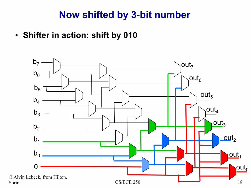
Now shifted by 3-bit number
• Shifter in action: shift by 010
CS/ECE 250
b0
b1
b2
b3
b4
b7
b6
b5
0 out0
out1
out2
out3
out4
out5
out6
out7

19 © Alvin Lebeck, from Hilton, Sorin
Now shifted by 3-bit number
• Shifter in action: shift by 011
CS/ECE 250
b0
b1
b2
b3
b4
b7
b6
b5
0 out0
out1
out2
out3
out4
out5
out6
out7

20 © Alvin Lebeck, from Hilton, Sorin CS/ECE 250
So far…
• We can make logic to compute “math” − Add, subtract,… (we’ll see multiply/divide later) − Bitwise: AND, OR, NOT,… − Shifts − Selection (MUX)
• But processors need state (hold value) − Registers

21 © Alvin Lebeck, from Hilton, Sorin CS/ECE 250
Memory Elements
• All the circuits we looked at so far are combinational circuits: the output is a Boolean function of the inputs.
• We need circuits that can remember values (registers, memory)
• The output of the circuit is a function of the input and a stored value (state)
• Circuits with memory are called sequential circuits
• Key to storage: loops in circuit from outputs to inputs
22 © Alvin Lebeck, from Hilton, Sorin CS/ECE 250
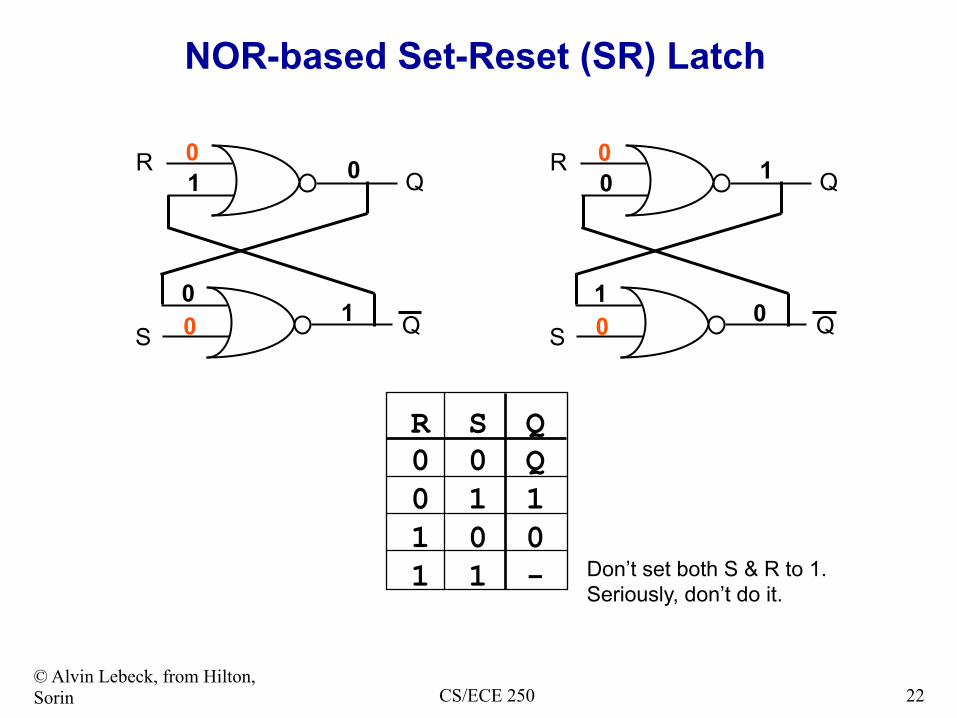
NOR-based Set-Reset (SR) Latch
R
S
Q
Q
0 1 0
1 0 0
R
S
Q
Q
0 0 1
0 1 0
R S Q 0 0 Q 0 1 1 1 0 0 1 1 - Don’t set both S & R to 1.
Seriously, don’t do it.

23 © Alvin Lebeck, from Hilton, Sorin CS/ECE 250
R
S
Q
Q
0 1 0
1 0 0
R
S
Q
Q
0 0 1
0 1 1
Set-Reset Latch (Continued)
Time
S 0 1
R 0 1
Q 0 1

24 © Alvin Lebeck, from Hilton, Sorin CS/ECE 250
R
S
Q
Q
0 1 0
1 0 0
R
S
Q
Q
0 0 1
0 1 1
Set-Reset Latch (Continued)
Time
S 0 1
R 0 1
Q 0 1
Set Signal Goes High
Output Signal Goes High

25 © Alvin Lebeck, from Hilton, Sorin CS/ECE 250
R
S
Q
Q
0 1 0
1 0 0
R
S
Q
Q
0 0 1
0 1 1
Set-Reset Latch (Continued)
Time
S 0 1
R 0 1
Q 0 1
Set Signal Goes Low
Output Signal Stays High

26 © Alvin Lebeck, from Hilton, Sorin CS/ECE 250
R
S
Q
Q
0 1 0
1 0 0
R
S
Q
Q
0 0 1
0 1 1
Set-Reset Latch (Continued)
Time
S 0 1
R 0 1
Q 0 1
Until Reset Signal Goes High
Then Output Signal Goes Low

27 © Alvin Lebeck, from Hilton, Sorin CS/ECE 250
SR Latch
• Downside: S and R at once = chaos
• Downside: Bad interface
• What is a better solution?

28 © Alvin Lebeck, from Hilton, Sorin CS/ECE 250
Data Latch (D Latch)
Q
Q
Starting with SR Latch

29 © Alvin Lebeck, from Hilton, Sorin CS/ECE 250
Data Latch (D Latch)
Data
Enable Q
Q
Starting with SR Latch Change interface to Data + Enable (D + E)
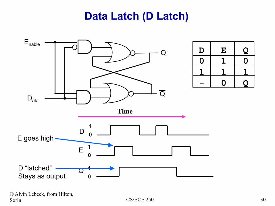
30 © Alvin Lebeck, from Hilton, Sorin CS/ECE 250
Data Latch (D Latch)
Data
Enable Q
Q
D E Q 0 1 0 1 1 1 - 0 Q
Time
D 0 1
E 0 1
Q 0 1
E goes high
D “latched” Stays as output

31 © Alvin Lebeck, from Hilton, Sorin CS/ECE 250
Data Latch (D Latch)
Data
Enable Q
Q
D E Q 0 1 0 1 1 1 - 0 Q
Time
D 0 1
E 0 1
Q 0 1
Does not affect Output
E goes low
Output unchanged By changes to D

32 © Alvin Lebeck, from Hilton, Sorin CS/ECE 250
Data Latch (D Latch)
Data
Enable Q
Q
D E Q 0 1 0 1 1 1 - 0 Q
Time
D 0 1
E 0 1
Q 0 1
E goes high
D “latched” Becomes new output

33 © Alvin Lebeck, from Hilton, Sorin CS/ECE 250
Data Latch (D Latch)
Data
Enable Q
Q
D E Q 0 1 0 1 1 1 - 0 Q
Time
D 0 1
E 0 1
Q 0 1
Slight Delay
(Logic gates take time)
34 © Alvin Lebeck, from Hilton, Sorin CS/ECE 250
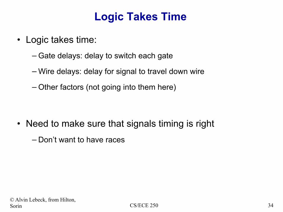
Logic Takes Time
• Logic takes time: − Gate delays: delay to switch each gate
− Wire delays: delay for signal to travel down wire
− Other factors (not going into them here)
• Need to make sure that signals timing is right − Don’t want to have races

35 © Alvin Lebeck, from Hilton, Sorin
Clocks
• Processors have a clock: − Alternates 0 1 0 1 (low high low high) − Latch à logic à latch in one clock cycle
− 3.4 GHz processor = 3.4 Billion clock cycles/sec
CS/ECE 250
One clock cycle

36 © Alvin Lebeck, from Hilton, Sorin
Level Triggered Clock
• First thoughts: Level Triggered − Latch enabled when clock is high − Hold value when clock is low
CS/ECE 250
D latch
D Q
E Q
D latch
D Q
E Q Logic
Clk
3 3

37 © Alvin Lebeck, from Hilton, Sorin
Level Triggered Clock
• How we’d like this to work − Clock is low, all values stable
CS/ECE 250
D latch
D Q
E Q
D latch
D Q
E Q Logic
Clk
3 3
010 111 100 001
0
Clk

38 © Alvin Lebeck, from Hilton, Sorin
Level Triggered Clock
• How we’d like this to work − Clock goes high, latches capture and transmit new value
CS/ECE 250
D latch
D Q
E Q
D latch
D Q
E Q Logic
Clk
3 3
010 010 100 100
0
Clk

39 © Alvin Lebeck, from Hilton, Sorin
Level Triggered Clock
• How we’d like this to work − Signals work their way through logic w/ high clk
CS/ECE 250
D latch
D Q
E Q
D latch
D Q
E Q Logic
Clk
3 3
010 010 100 100
0
Clk

40 © Alvin Lebeck, from Hilton, Sorin
Level Triggered Clock
• How we’d like this to work − Clock goes low before signals reach next latch
CS/ECE 250
D latch
D Q
E Q
D latch
D Q
E Q Logic
Clk
3 3
010 010 100 100
0
Clk
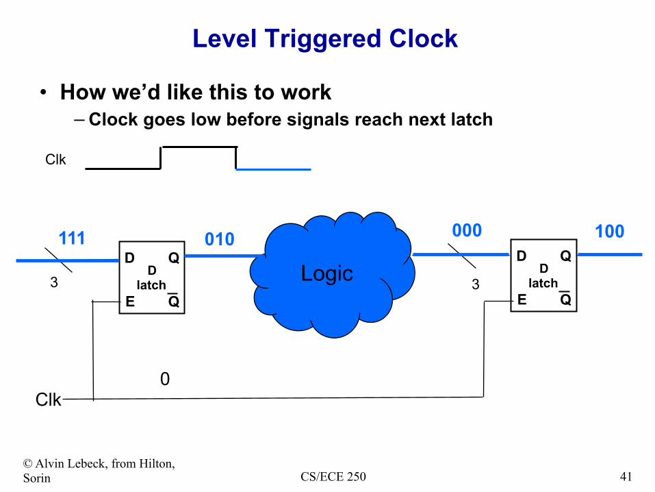
41 © Alvin Lebeck, from Hilton, Sorin
Level Triggered Clock
• How we’d like this to work − Clock goes low before signals reach next latch
CS/ECE 250
D latch
D Q
E Q
D latch
D Q
E Q Logic
Clk
3 3
111 010 000 100
0
Clk

42 © Alvin Lebeck, from Hilton, Sorin
Level Triggered Clock
• How we’d like this to work − Everything stable before clk goes high
CS/ECE 250
D latch
D Q
E Q
D latch
D Q
E Q Logic
Clk
3 3
111 010 000 100
0
Clk

43 © Alvin Lebeck, from Hilton, Sorin
Level Triggered Clock
• How we’d like this to work − Clk goes high again, repeat
CS/ECE 250
D latch
D Q
E Q
D latch
D Q
E Q Logic
Clk
3 3
111 111 000 000
0
Clk

44 © Alvin Lebeck, from Hilton, Sorin
Level Triggered Clock
• Problem: What if signal reaches latch too early? − i.e., while clk is still high
CS/ECE 250
D latch
D Q
E Q
D latch
D Q
E Q Logic
Clk
3 3
111 111 101 000
0
Clk

45 © Alvin Lebeck, from Hilton, Sorin
Level Triggered Clock
• Problem: What if signal reaches latch too early? − Signal goes right through latch, into next stage..
CS/ECE 250
D latch
D Q
E Q
D latch
D Q
E Q Logic
Clk
3 3
111 111 101 101
0
Clk

46 © Alvin Lebeck, from Hilton, Sorin
That would be bad…
• Getting into a stage too early is bad − Something else is going on there à corrupted − Also may be a loop with one latch
• Consider incrementing counter (or PC) − Too fast -- increment twice? Not good.
CS/ECE 250
D latch
D Q
E Q
+1
3
001
010
47 © Alvin Lebeck, from Hilton, Sorin
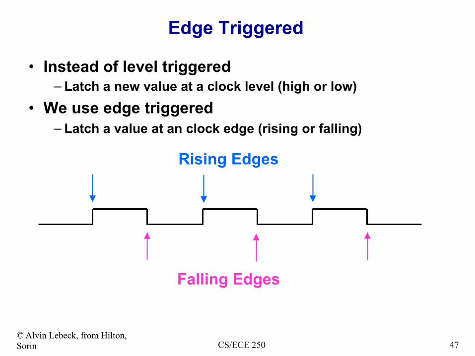
Edge Triggered
• Instead of level triggered − Latch a new value at a clock level (high or low)
• We use edge triggered − Latch a value at an clock edge (rising or falling)
CS/ECE 250
Rising Edges
Falling Edges
48 © Alvin Lebeck, from Hilton, Sorin
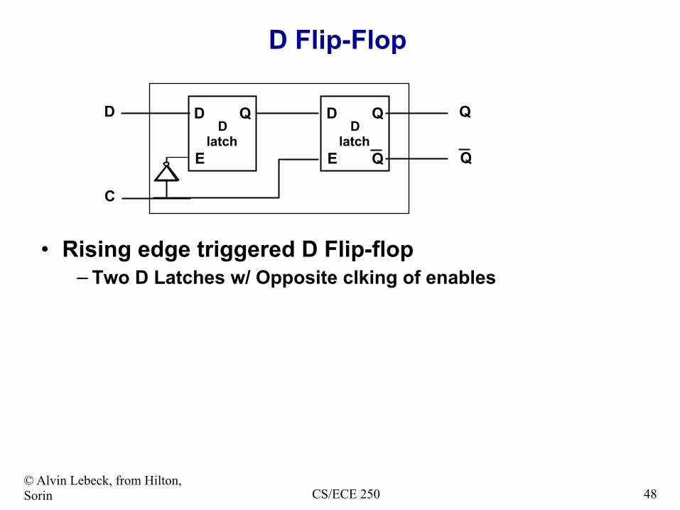
D Flip-Flop
• Rising edge triggered D Flip-flop − Two D Latches w/ Opposite clking of enables
CS/ECE 250
D latch
D Q
E
D latch
D Q
E Q Q
Q D
C

49 © Alvin Lebeck, from Hilton, Sorin
D Flip-Flop
• Rising edge triggered D Flip-flop − Two D Latches w/ opposite clking of enables
− On Low Clk, first latch enabled (propagates value) • Second not enabled, maintains value
CS/ECE 250
D latch
D Q
E
D latch
D Q
E Q Q
Q D
C

50 © Alvin Lebeck, from Hilton, Sorin
D Flip-Flop
• Rising edge triggered D Flip-flop − Two D Latches w/ opposite clking of enables
− On Low Clk, first latch enabled (propagates value) • Second not enabled, maintains value
− On High Clk, second latch enabled • First latch not enabled, maintains value
CS/ECE 250
D latch
D Q
E
D latch
D Q
E Q Q
Q D
C

51 © Alvin Lebeck, from Hilton, Sorin
D Flip-Flop
• No possibility of “races” − Even if I put 2 DFFs back-to-back… − By the time signal gets through 2nd latch of 1st DFF, 1st latch of 2nd DFF is disabled
• Still must ensure signals reach DFF before clk rises − Important concern in logic design is “making timing”
CS/ECE 250
D latch
D Q
E
D latch
D Q
E Q
D
C
D latch
D Q
E
D latch
D Q
E Q
C

52 © Alvin Lebeck, from Hilton, Sorin
D Flip-flops (continued…)
• Could also do falling edge triggered − Switch which latch has NOT on clk
• D Flip-flop is ubiquitous − Typically people just say “latch” and mean DFF − Which edge is used does not matter
• As long as same edge is used consistently • We will use rising edge
CS/ECE 250

53 © Alvin Lebeck, from Hilton, Sorin
D flip flops
• Generally do not draw clk input − Have one global clk, assume it goes there − Often see > as symbol meaning clk
• Maybe have explicit enable − Might not want to write every cycle − If no enable signal shown, implies always enabled
• Get output and NOT(output) for “free”
CS/ECE 250
DFF D Q
E Q
DFF D Q
Q
DFF D Q
> Q

54 © Alvin Lebeck, from Hilton, Sorin CS/ECE 250
Register File
• Can store one value…what about manyvalues ? • E.g., Register File (the physical storage for the regs)
− MIPS, 32 32-bit integer registers
• How do we build a Register File using D Flip-Flops? • What other components do we need?

55 © Alvin Lebeck, from Hilton, Sorin
• Reading the registers − 32 input mux -- slow − Need 32 32-1 MUXes -- big − Other regs not pictured
Register File
CS/ECE 250
32 bit reg D Q
E Q
32 bit reg D Q
E Q
32 bit reg D Q
E Q
32 bit reg D Q
E Q
… …

56 © Alvin Lebeck, from Hilton, Sorin
Register File
• Reading the registers − 32 input mux -- slow − Need 32 32-1 MUXes -- big − Other regs not pictured
• Writing the registers − Need to pick which reg − Have reg num (e.g., 19) − Make En19=1
• En0, En1,… = 0
CS/ECE 250
32 bit reg D Q
E Q
32 bit reg D Q
E Q
32 bit reg D Q
E Q
32 bit reg D Q
E Q
… … WrData
En0
En1
En30
En31

57 © Alvin Lebeck, from Hilton, Sorin
Decoders
• First task: convert binary number to “one hot” − N bits in − 2N bits out − 2N-1 bits are 0, 1 bit (matching the input) is 1
CS/ECE 250
Dec
oder
3
101 0
0 0
0 0
1 0
0

58 © Alvin Lebeck, from Hilton, Sorin
Decoder Logic
• Decoder basically AND gates for each output: − Out0 only True (one) if input 000
CS/ECE 250
In0
In1
In2
Out0
3-input gates are fine. In theory, gates can have any # of inputs In practice >4 converted to multiple gates

59 © Alvin Lebeck, from Hilton, Sorin
Decoder Logic
• Decoder basically AND gates for each output: − Out1 only True (one) if input 001
CS/ECE 250
In0
In1
In2
Out0
Out1
Repeat for all outputs AND together correct sets of bits

60 © Alvin Lebeck, from Hilton, Sorin
Register File
• Decoder supports register addressing: − Use decoder to convert register number into control signal − Send write data to all registers − Use one hot encoding to enable destination register
• Need to fix register read speed − 32 input mux is not realistic − For tractability, expand our world from {1,0} to {1, 0, Z}
CS/ECE 250

61 © Alvin Lebeck, from Hilton, Sorin
Water Analogy
• To understand Z, let’s make an analogy − Think of a wire as a pipe
• Has water = 1 • Has water = 0
− This wire is 0 (it has no water)
CS/ECE 250

62 © Alvin Lebeck, from Hilton, Sorin
Water Analogy
• To understand Z, let’s make an analogy − Think of a wire as a pipe
• Has water = 1 • Has water = 0
− This wire is 1 (its full of water)
CS/ECE 250

63 © Alvin Lebeck, from Hilton, Sorin
Water Analogy
• To understand Z, let’s make an analogy − Think of a wire as a pipe
• Has water = 1 • Has water = 0
− Suppose a gate drives a 0 onto this wire • Drain the water
CS/ECE 250
0

64 © Alvin Lebeck, from Hilton, Sorin
Water Analogy
• To understand Z, let’s make an analogy − Think of a wire as a pipe
• Has water = 1 • Has water = 0
− Suppose a gate drives a 0 onto this wire • Drain the water
CS/ECE 250
0

65 © Alvin Lebeck, from Hilton, Sorin
Water Analogy
• To understand Z, let’s make an analogy − Think of a wire as a pipe
• Has water = 1 • Has water = 0
− Suppose a gate drives a 0 onto this wire • Drain the water
CS/ECE 250
0

66 © Alvin Lebeck, from Hilton, Sorin
Water Analogy
• To understand Z, let’s make an analogy − Think of a wire as a pipe
• Has water = 1 • Has water = 0
− Suppose a gate drives a 0 onto this wire • Drain the water
CS/ECE 250
0

67 © Alvin Lebeck, from Hilton, Sorin
Water Analogy
• To understand Z, let’s make an analogy − Think of a wire as a pipe
• Has water = 1 • Has water = 0
− Suppose the gate now drives a 1 • Pump the water
CS/ECE 250
1

68 © Alvin Lebeck, from Hilton, Sorin
Water Analogy
• To understand Z, let’s make an analogy − Think of a wire as a pipe
• Has water = 1 • Has water = 0
− Suppose the gate now drives a 1 • Pump the water
CS/ECE 250
1

69 © Alvin Lebeck, from Hilton, Sorin
Water Analogy
• To understand Z, let’s make an analogy − Think of a wire as a pipe
• Has water = 1 • Has water = 0
− Suppose the gate now drives a 1 • Pump the water
CS/ECE 250
1

70 © Alvin Lebeck, from Hilton, Sorin
Remember this rule?
• Do not connect two outputs to the same wire
• One gate drives 1. The other drives 0. − One pumps water in. The other drains water out − Except it’s not water, it’s electric charge − “Short circuit” à lots of current à lots of heat
CS/ECE 250
a b
c d
BAD!

71 © Alvin Lebeck, from Hilton, Sorin
A third option: Z
• There is a third possibility: Z (“high impedance”) − Neither pumping or draining charge − Prevents charge from flowing through
• Gate that gives us Z : Tri-state
CS/ECE 250
D E Q 0 1 0 1 1 1 - 0 Z
D Q
E

72 © Alvin Lebeck, from Hilton, Sorin CS/ECE 250
It’s ok to connect multiple outputs together under one circumstance -- all but one must be outputting Z at any time
D0
E0
D1
E1
Dn-2
En-2
Dn-1
En-1
Tri-State Buffers

73 © Alvin Lebeck, from Hilton, Sorin
Mux with Tri-State Buffers
− Much more efficient for large #s of inputs (e.g., 32)
− Decoder ensures only one output
CS/ECE 250
Dec
oder
5
11110 0
0
1 0
32 bit reg D Q
E Q
32 bit reg D Q
E Q
32 bit reg D Q
E Q
32 bit reg D Q
E Q
… …
… …

74 © Alvin Lebeck, from Hilton, Sorin
Ports
• Read Ports − Ability to do one read per clock cycle
− May want more -- read two source registers per instruction • Maybe even more if we do many instrs at once (later…)
− Could add more: need to replicate port • Another decoder • Another set of tri-states • Another output bus (wire connecting the tri-states)
• Write Ports − Ability to do one write/cycle − Could add more: need to multiplex write values
CS/ECE 250

75 © Alvin Lebeck, from Hilton, Sorin
Minor Detail
• This is not how a register file is implemented in today’s processors − (Though it is how other things are implemented) − Actually done with SRAM − We’ll see that later this semester…
CS/ECE 250