Embed Size (px)
Citation preview

1
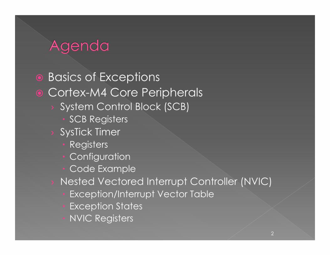
Basics of ExceptionsCortex-M4 Core Peripherals› System Control Block (SCB)
SCB Registers› SysTick Timer
Registers Configuration Code Example
› Nested Vectored Interrupt Controller (NVIC)Exception/Interrupt Vector TableException StatesNVIC Registers
2
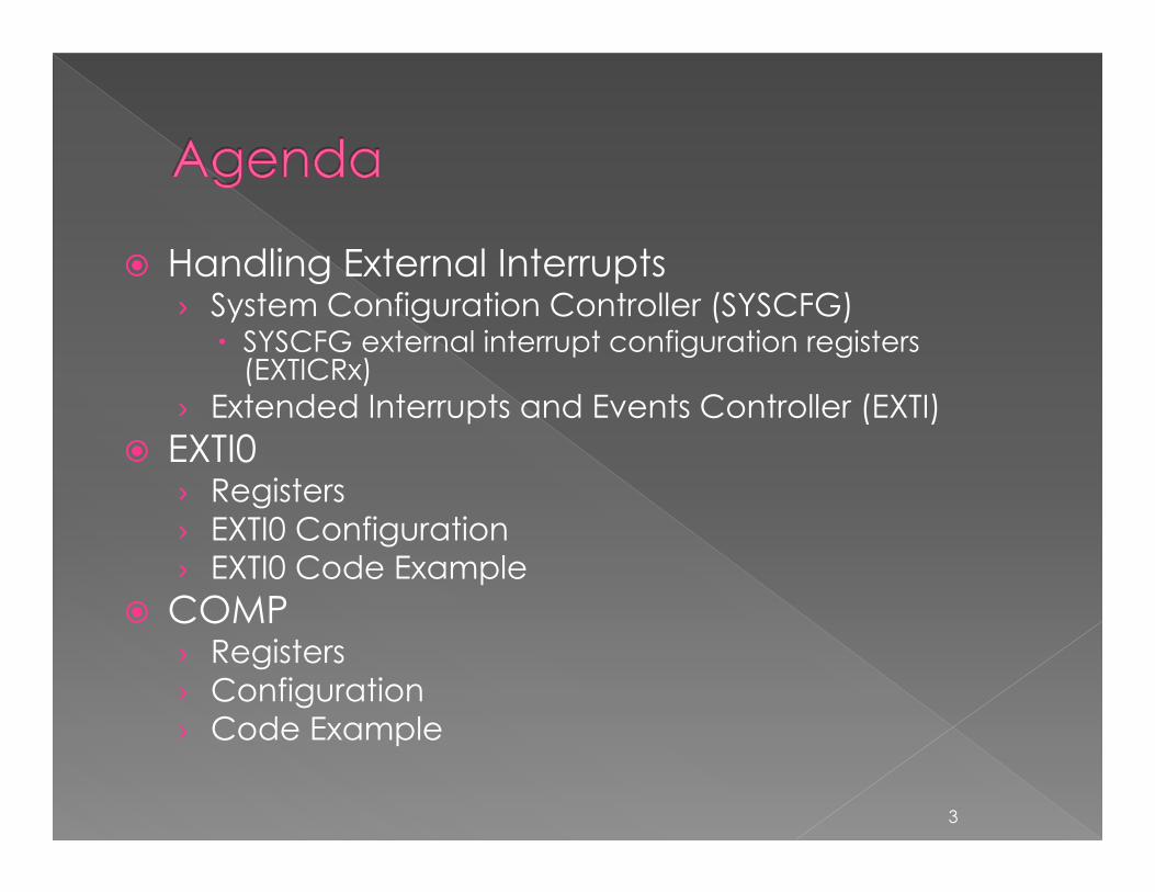
Handling External Interrupts › System Configuration Controller (SYSCFG)
SYSCFG external interrupt configuration registers (EXTICRx)
› Extended Interrupts and Events Controller (EXTI)EXTI0› Registers› EXTI0 Configuration› EXTI0 Code ExampleCOMP› Registers› Configuration› Code Example
3

4
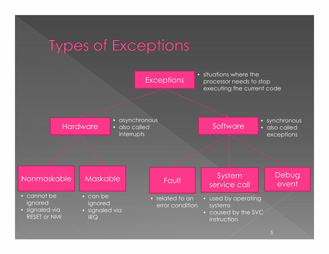
Exceptions
Hardware Software
Nonmaskable Maskable
• cannot be ignored
• signaled via RESET or NMI
Fault System service call
• can be ignored
• signaled via IRQ
• asynchronous• also called
interrupts
• synchronous• also called
exceptions
Debug event
• related to an error condition
• situations where the processor needs to stop executing the current code
• used by operating systems
• caused by the SVC instruction
5
6
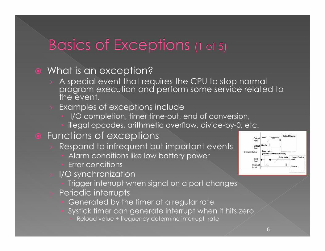
What is an exception?› A special event that requires the CPU to stop normal
program execution and perform some service related to the event.
› Examples of exceptions includeI/O completion, timer time-out, end of conversion, illegal opcodes, arithmetic overflow, divide-by-0, etc.
Functions of exceptions› Respond to infrequent but important events
Alarm conditions like low battery powerError conditions
› I/O synchronizationTrigger interrupt when signal on a port changes
› Periodic interruptsGenerated by the timer at a regular rateSystick timer can generate interrupt when it hits zero
Reload value + frequency determine interrupt rate
7
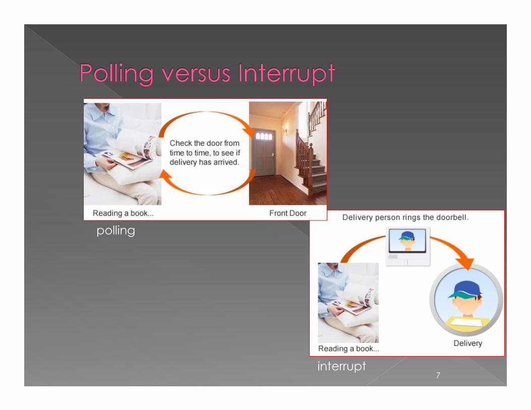
polling
interrupt
8
Interrupt maskability› Interrupts that can be ignored by the CPU are called maskable
interrupts. › A maskable interrupt must be enabled before it can interrupt the
CPU. › An interrupt is enabled by setting an enable bit.› Interrupts that can’t be ignored by the CPU are called
nonmaskable interrupts.Exception priority› Allow multiple pending interrupt requests› Resolve the order of service for multiple pending interrupts
Interrupt service routine› An interrupt handler, also known as an Interrupt Service Routine
(ISR), is a callback subroutine in microcontroller firmware whose execution is triggered by the reception of an interrupt.
› Interrupt handlers have a multitude of functions, which vary based on the reason the interrupt was generated.
9
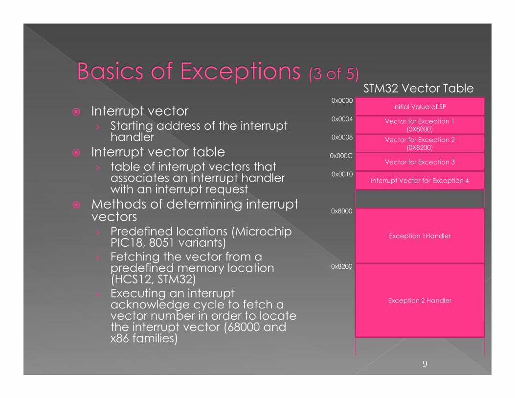
Interrupt vector› Starting address of the interrupt
handlerInterrupt vector table› table of interrupt vectors that
associates an interrupt handler with an interrupt request
Methods of determining interrupt vectors› Predefined locations (Microchip
PIC18, 8051 variants)› Fetching the vector from a
predefined memory location (HCS12, STM32)
› Executing an interrupt acknowledge cycle to fetch a vector number in order to locate the interrupt vector (68000 and x86 families)
Initial Value of SP
Vector for Exception 1(0X8000)
0x0000
0x0004
Vector for Exception 2(0X8200)
0x0008
Vector for Exception 30x000C
Interrupt Vector for Exception 40x0010
Exception 1Handler
Exception 2 Handler
0x8000
0x8200
STM32 Vector Table
10
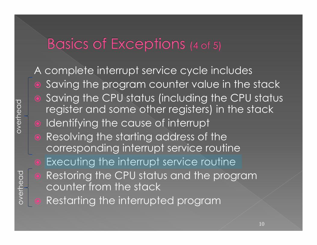
A complete interrupt service cycle includesSaving the program counter value in the stackSaving the CPU status (including the CPU status register and some other registers) in the stackIdentifying the cause of interruptResolving the starting address of the corresponding interrupt service routineExecuting the interrupt service routineRestoring the CPU status and the program counter from the stackRestarting the interrupted program
over
head
over
head

Interrupt is a powerful concept in embedded systems for separating the time-critical events from the others and execute them in a prioritized manner. In a typical embedded system, the embedded processor (microcontroller) is responsible for doing more than one task (but can do only one at a time).
Programmable Room Temperature Control 11
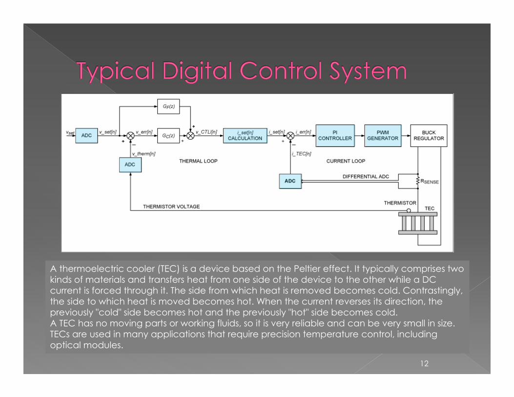
A thermoelectric cooler (TEC) is a device based on the Peltier effect. It typically comprises two kinds of materials and transfers heat from one side of the device to the other while a DC current is forced through it. The side from which heat is removed becomes cold. Contrastingly, the side to which heat is moved becomes hot. When the current reverses its direction, the previously "cold" side becomes hot and the previously "hot" side becomes cold. A TEC has no moving parts or working fluids, so it is very reliable and can be very small in size. TECs are used in many applications that require precision temperature control, including optical modules.
12

13
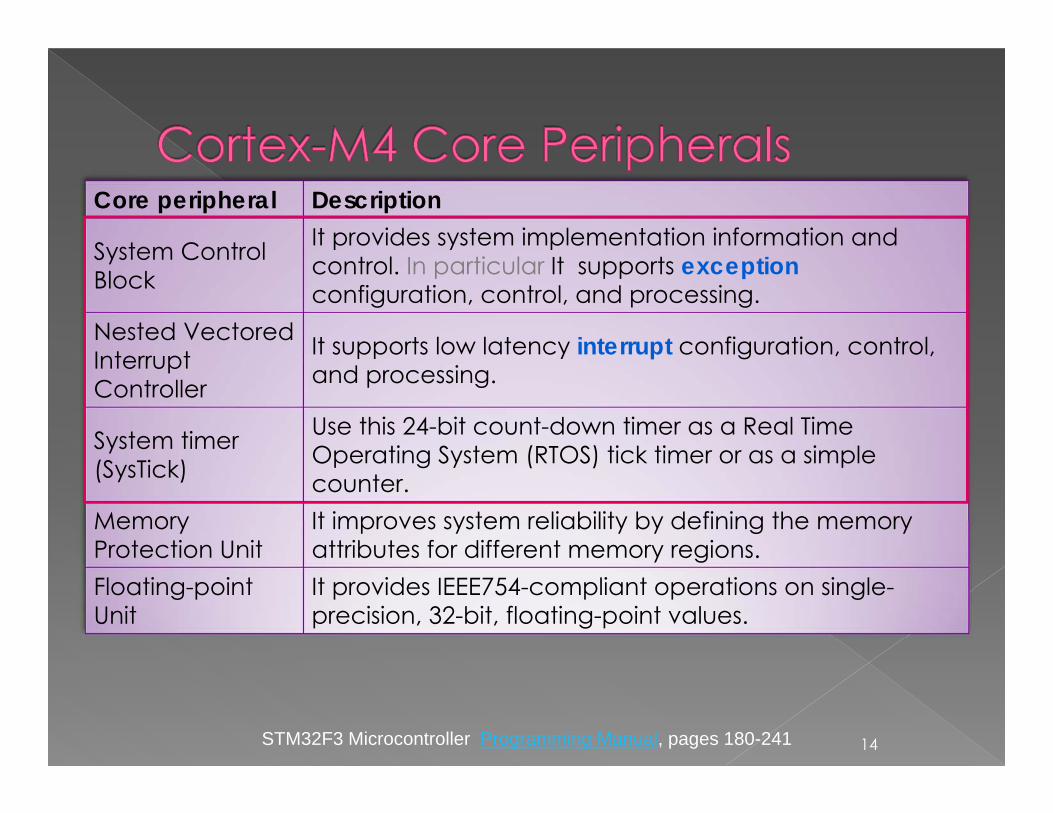
Core peripheral Description
System Control Block
It provides system implementation information and control. In particular It supports exceptionconfiguration, control, and processing.
Nested Vectored Interrupt Controller
It supports low latency interrupt configuration, control,and processing.
System timer(SysTick)
Use this 24-bit count-down timer as a Real Time Operating System (RTOS) tick timer or as a simple counter.
Memory Protection Unit
It improves system reliability by defining the memory attributes for different memory regions.
Floating-point Unit
It provides IEEE754-compliant operations on single-precision, 32-bit, floating-point values.
STM32F3 Microcontroller Programming Manual, pages 180-241 14

15
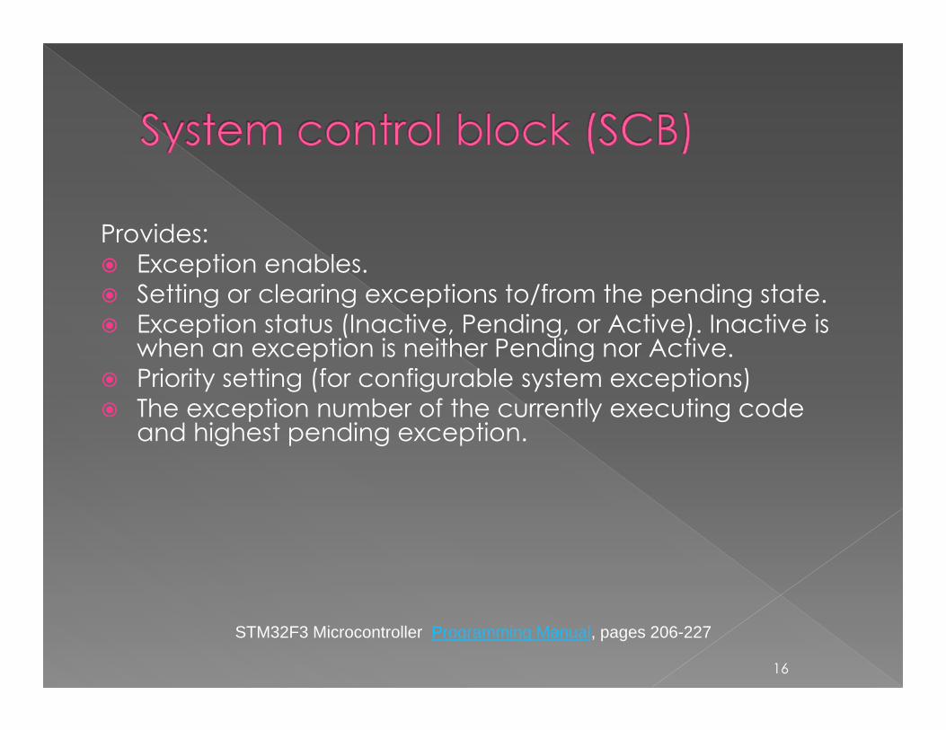
Provides:Exception enables.Setting or clearing exceptions to/from the pending state.Exception status (Inactive, Pending, or Active). Inactive is when an exception is neither Pending nor Active.Priority setting (for configurable system exceptions)The exception number of the currently executing code and highest pending exception.
STM32F3 Microcontroller Programming Manual, pages 206-227
16

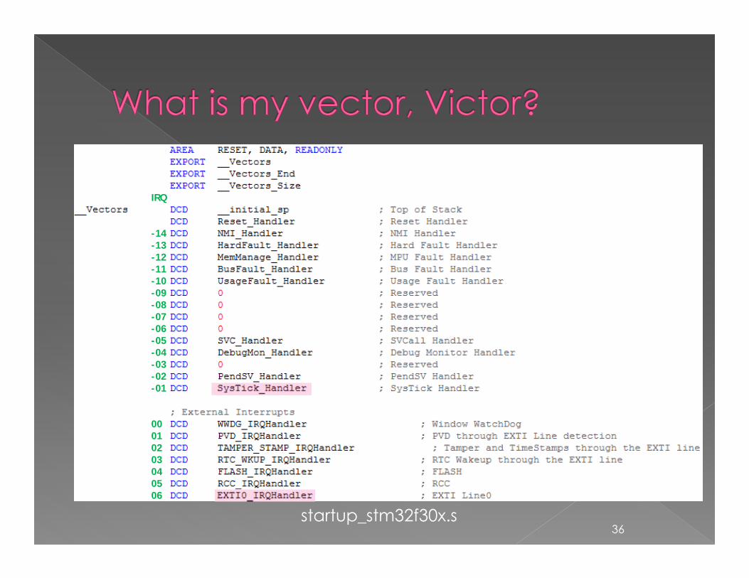
startup_stm32f30x.s
IRQ #
-14-13-12-11-10-09-08-07-06-05-04-03-02-01
00010203040506
17
Exceptions
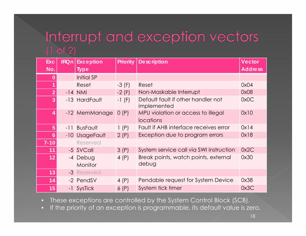
ExcNo.
IRQn Exception Type
Priority Description Vector Address
0 Initial SP1 Reset -3 (F) Reset 0x042 -14 NMI -2 (F) Non-Maskable Interrupt 0x083 -13 HardFault -1 (F) Default fault if other handler not
implemented0x0C
4 -12 MemManage 0 (P) MPU violation or access to illegal locations
0x10
5 -11 BusFault 1 (P) Fault if AHB interface receives error 0x146 -10 UsageFault 2 (P) Exception due to program errors 0x18
7-10 Reserved11 -5 SVCall 3 (P) System service call via SWI instruction 0x2C12 -4 Debug
Monitor4 (P) Break points, watch points, external
debug0x30
13 -3 Reserved14 -2 PendSV 4 (P) Pendable request for System Device 0x3815 -1 SysTick 6 (P) System tick timer 0x3C
• These exceptions are controlled by the System Control Block (SCB).• If the priority of an exception is programmable, its default value is zero.
18
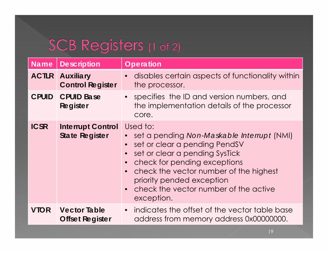
Name Description OperationACTLR Auxiliary
Control Register• disables certain aspects of functionality within
the processor.CPUID CPUID Base
Register• specifies the ID and version numbers, and
the implementation details of the processor core.
ICSR Interrupt ControlState Register
Used to:• set a pending Non-Maskable Interrupt (NMI)• set or clear a pending PendSV• set or clear a pending SysTick• check for pending exceptions• check the vector number of the highest
priority pended exception• check the vector number of the active
exception.VTOR Vector Table
Offset Register• indicates the offset of the vector table base
address from memory address 0x00000000.19
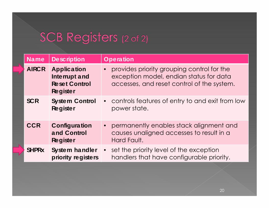
Name Description OperationAIRCR Application
Interrupt and Reset Control Register
• provides priority grouping control for the exception model, endian status for data accesses, and reset control of the system.
SCR System Control Register
• controls features of entry to and exit from low power state.
CCR Configurationand ControlRegister
• permanently enables stack alignment and causes unaligned accesses to result in a Hard Fault.
SHPRx System handler priority registers
• set the priority level of the exception handlers that have configurable priority.
20
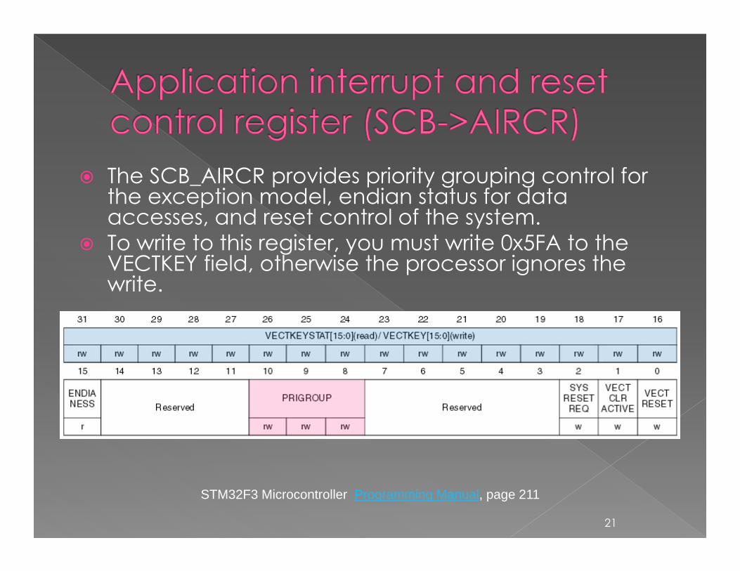
The SCB_AIRCR provides priority grouping control for the exception model, endian status for data accesses, and reset control of the system.To write to this register, you must write 0x5FA to the VECTKEY field, otherwise the processor ignores the write.
21
STM32F3 Microcontroller Programming Manual, page 211
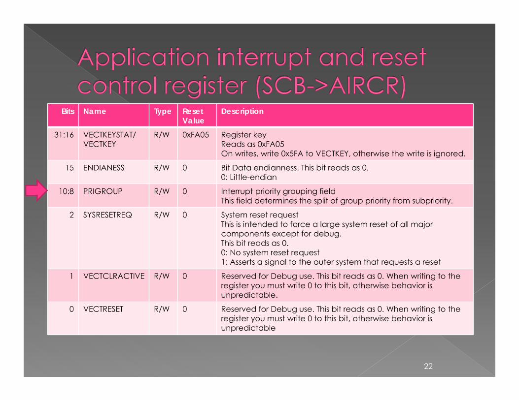
Bits Name Type Reset Value
Description
31:16 VECTKEYSTAT/ VECTKEY
R/W 0xFA05 Register keyReads as 0xFA05On writes, write 0x5FA to VECTKEY, otherwise the write is ignored.
15 ENDIANESS R/W 0 Bit Data endianness. This bit reads as 0.0: Little-endian
10:8 PRIGROUP R/W 0 Interrupt priority grouping fieldThis field determines the split of group priority from subpriority.
2 SYSRESETREQ R/W 0 System reset requestThis is intended to force a large system reset of all major components except for debug.This bit reads as 0.0: No system reset request1: Asserts a signal to the outer system that requests a reset
1 VECTCLRACTIVE R/W 0 Reserved for Debug use. This bit reads as 0. When writing to the register you must write 0 to this bit, otherwise behavior is unpredictable.
0 VECTRESET R/W 0 Reserved for Debug use. This bit reads as 0. When writing to the register you must write 0 to this bit, otherwise behavior is unpredictable
22
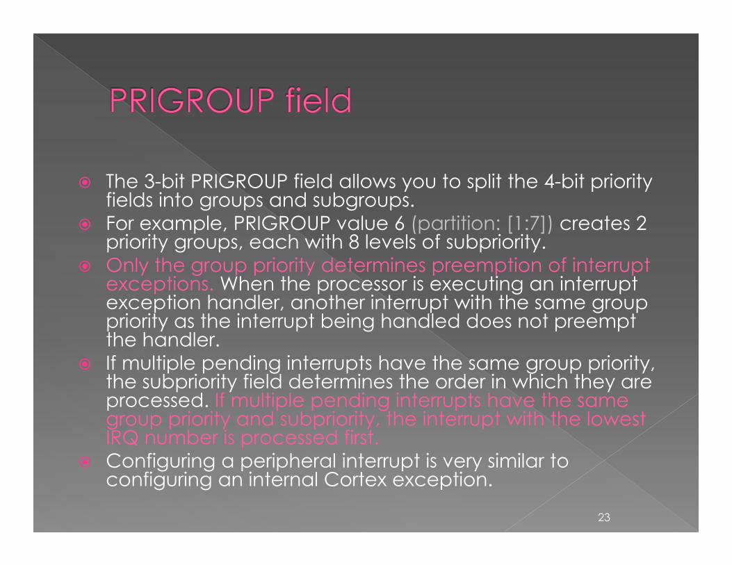
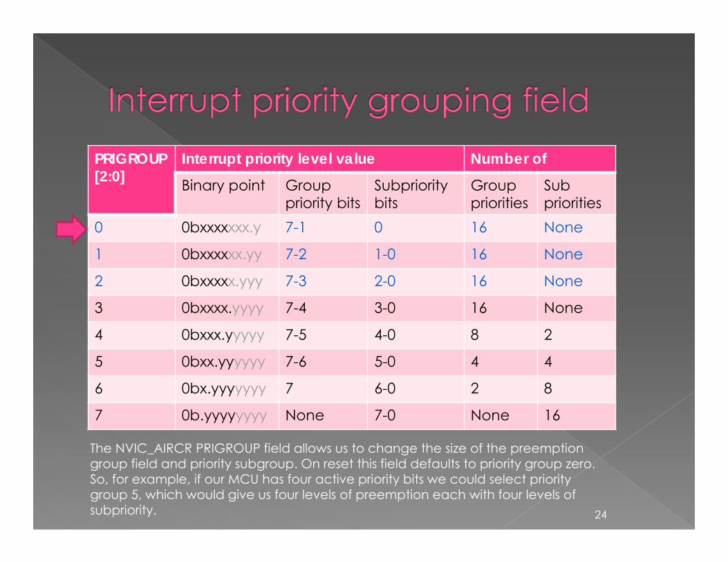
The 3-bit PRIGROUP field allows you to split the 4-bit priority fields into groups and subgroups. For example, PRIGROUP value 6 (partition: [1:7]) creates 2 priority groups, each with 8 levels of subpriority. Only the group priority determines preemption of interrupt exceptions. When the processor is executing an interrupt exception handler, another interrupt with the same group priority as the interrupt being handled does not preempt the handler.If multiple pending interrupts have the same group priority, the subpriority field determines the order in which they are processed. If multiple pending interrupts have the same group priority and subpriority, the interrupt with the lowest IRQ number is processed first.Configuring a peripheral interrupt is very similar to configuring an internal Cortex exception.
23
PRIGROUP [2:0]
Interrupt priority level value Number of
Binary point Group priority bits
Subprioritybits
Group priorities
Sub priorities
0 0bxxxxxxx.y 7-1 0 16 None
1 0bxxxxxx.yy 7-2 1-0 16 None
2 0bxxxxx.yyy 7-3 2-0 16 None
3 0bxxxx.yyyy 7-4 3-0 16 None
4 0bxxx.yyyyy 7-5 4-0 8 2
5 0bxx.yyyyyy 7-6 5-0 4 4
6 0bx.yyyyyyy 7 6-0 2 8
7 0b.yyyyyyyy None 7-0 None 16
The NVIC_AIRCR PRIGROUP field allows us to change the size of the preemption group field and priority subgroup. On reset this field defaults to priority group zero. So, for example, if our MCU has four active priority bits we could select priority group 5, which would give us four levels of preemption each with four levels of subpriority. 24
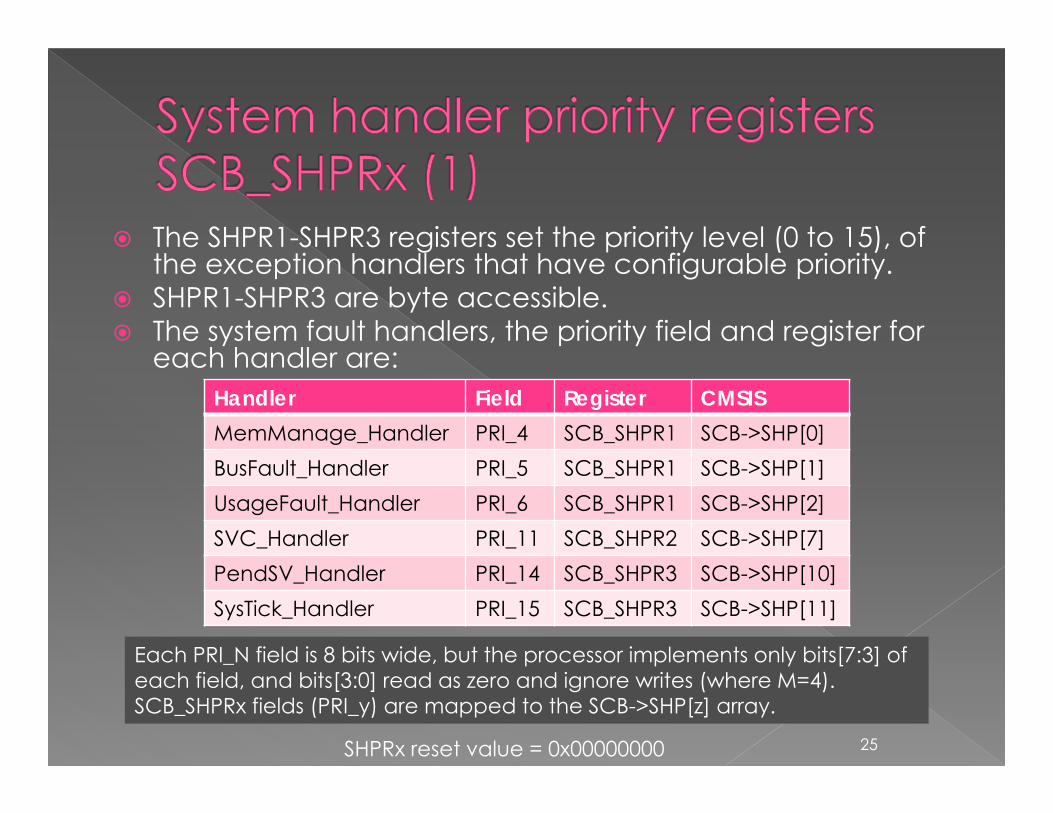
The SHPR1-SHPR3 registers set the priority level (0 to 15), of the exception handlers that have configurable priority.SHPR1-SHPR3 are byte accessible.The system fault handlers, the priority field and register for each handler are:
Each PRI_N field is 8 bits wide, but the processor implements only bits[7:3] of each field, and bits[3:0] read as zero and ignore writes (where M=4). SCB_SHPRx fields (PRI_y) are mapped to the SCB->SHP[z] array.
25
Handler Field Register CMSISMemManage_Handler PRI_4 SCB_SHPR1 SCB->SHP[0]BusFault_Handler PRI_5 SCB_SHPR1 SCB->SHP[1]UsageFault_Handler PRI_6 SCB_SHPR1 SCB->SHP[2]SVC_Handler PRI_11 SCB_SHPR2 SCB->SHP[7]PendSV_Handler PRI_14 SCB_SHPR3 SCB->SHP[10]SysTick_Handler PRI_15 SCB_SHPR3 SCB->SHP[11]
SHPRx reset value = 0x00000000

26
CMSIS name
Programming Manual name
27
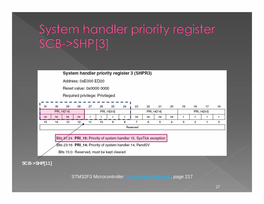
STM32F3 Microcontroller Programming Manual, page 217
SCB->SHP[11]
|
28
STM32F3 Microcontroller Programming Manual, pages 228-233
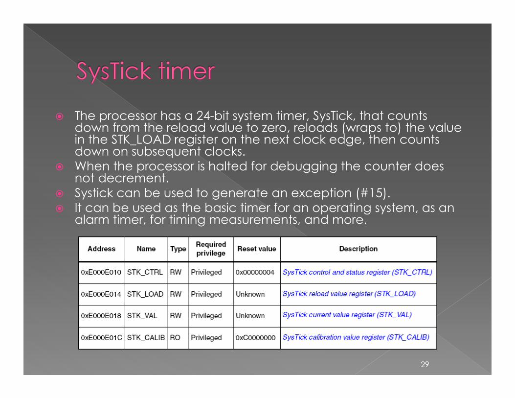
The processor has a 24-bit system timer, SysTick, that counts down from the reload value to zero, reloads (wraps to) the value in the STK_LOAD register on the next clock edge, then counts down on subsequent clocks.When the processor is halted for debugging the counter does not decrement.Systick can be used to generate an exception (#15).It can be used as the basic timer for an operating system, as an alarm timer, for timing measurements, and more.
29
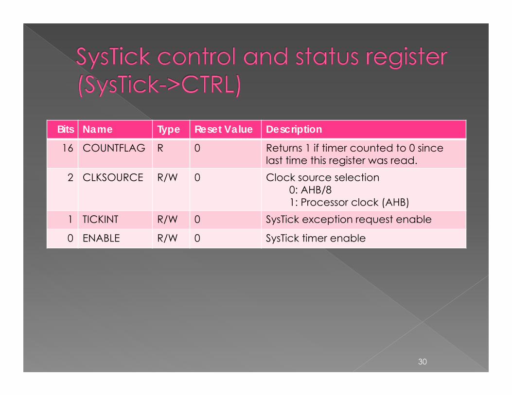
Bits Name Type Reset Value Description
16 COUNTFLAG R 0 Returns 1 if timer counted to 0 since last time this register was read.
2 CLKSOURCE R/W 0 Clock source selection0: AHB/81: Processor clock (AHB)
1 TICKINT R/W 0 SysTick exception request enable
0 ENABLE R/W 0 SysTick timer enable
30
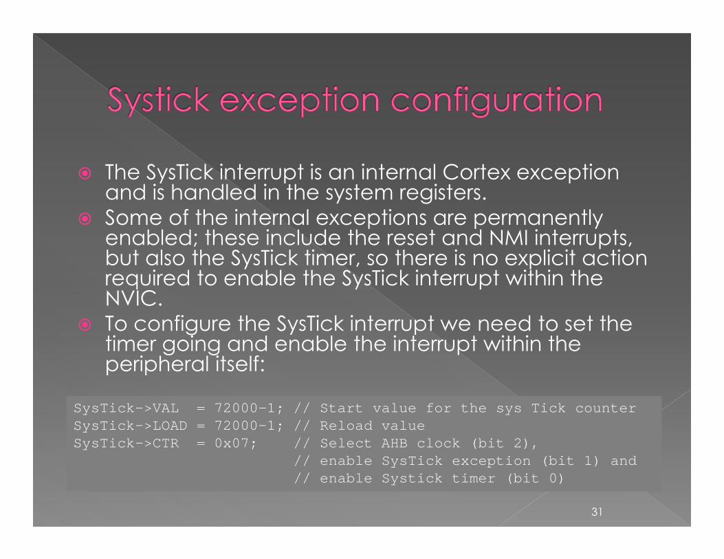
The SysTick interrupt is an internal Cortex exception and is handled in the system registers. Some of the internal exceptions are permanently enabled; these include the reset and NMI interrupts, but also the SysTick timer, so there is no explicit action required to enable the SysTick interrupt within the NVIC. To configure the SysTick interrupt we need to set the timer going and enable the interrupt within the peripheral itself:
SysTick->VAL = 72000-1; // Start value for the sys Tick counterSysTick->LOAD = 72000-1; // Reload valueSysTick->CTR = 0x07; // Select AHB clock (bit 2),
// enable SysTick exception (bit 1) and // enable Systick timer (bit 0)
31
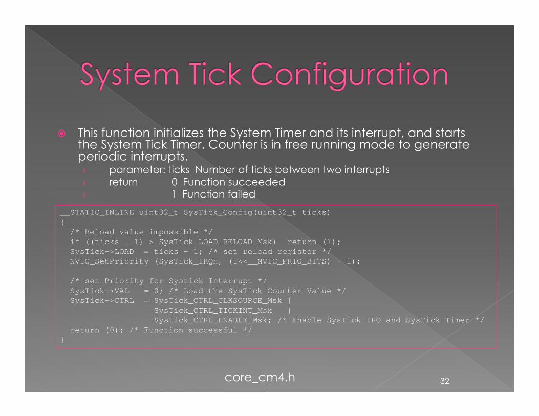
This function initializes the System Timer and its interrupt, and starts the System Tick Timer. Counter is in free running mode to generate periodic interrupts.› parameter: ticks Number of ticks between two interrupts› return 0 Function succeeded› 1 Function failed
__STATIC_INLINE uint32_t SysTick_Config(uint32_t ticks){
/* Reload value impossible */if ((ticks - 1) > SysTick_LOAD_RELOAD_Msk) return (1); SysTick->LOAD = ticks - 1; /* set reload register */NVIC_SetPriority (SysTick_IRQn, (1<<__NVIC_PRIO_BITS) - 1);
/* set Priority for Systick Interrupt */SysTick->VAL = 0; /* Load the SysTick Counter Value */SysTick->CTRL = SysTick_CTRL_CLKSOURCE_Msk |
SysTick_CTRL_TICKINT_Msk |SysTick_CTRL_ENABLE_Msk; /* Enable SysTick IRQ and SysTick Timer */
return (0); /* Function successful */}
core_cm4.h 32
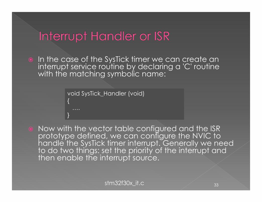
In the case of the SysTick timer we can create an interrupt service routine by declaring a 'C' routine with the matching symbolic name:
Now with the vector table configured and the ISR prototype defined, we can configure the NVIC to handle the SysTick timer interrupt. Generally we need to do two things: set the priority of the interrupt and then enable the interrupt source.
void SysTick_Handler (void){
….}
stm32f30x_it.c 33

34
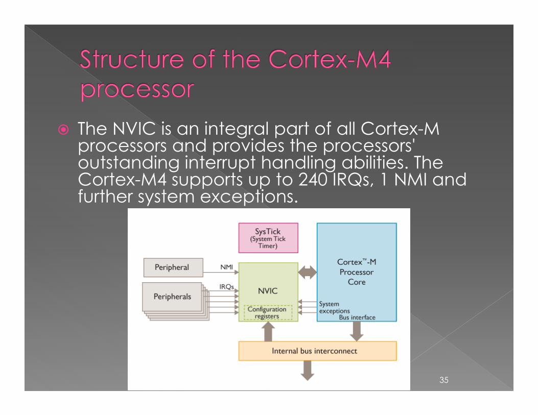
The NVIC is an integral part of all Cortex-M processors and provides the processors' outstanding interrupt handling abilities. The Cortex-M4 supports up to 240 IRQs, 1 NMI and further system exceptions.
35
startup_stm32f30x.s
IRQ
-14-13-12-11-10-09-08-07-06-05-04-03-02-01
00010203040506
36
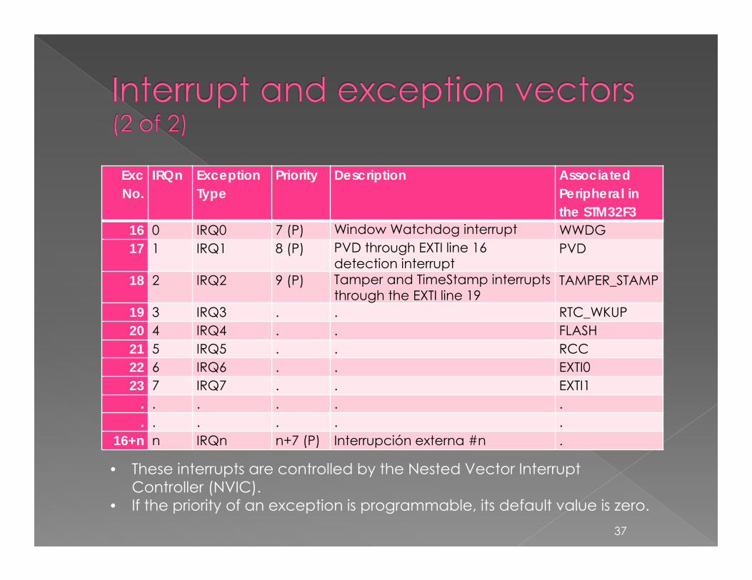
ExcNo.
IRQn ExceptionType
Priority Description AssociatedPeripheral in the STM32F3
16 0 IRQ0 7 (P) Window Watchdog interrupt WWDG17 1 IRQ1 8 (P) PVD through EXTI line 16
detection interruptPVD
18 2 IRQ2 9 (P) Tamper and TimeStamp interruptsthrough the EXTI line 19
TAMPER_STAMP
19 3 IRQ3 . . RTC_WKUP20 4 IRQ4 . . FLASH21 5 IRQ5 . . RCC22 6 IRQ6 . . EXTI023 7 IRQ7 . . EXTI1
. . . . . .
. . . . . .16+n n IRQn n+7 (P) Interrupción externa #n .
• These interrupts are controlled by the Nested Vector Interrupt Controller (NVIC).
• If the priority of an exception is programmable, its default value is zero.37
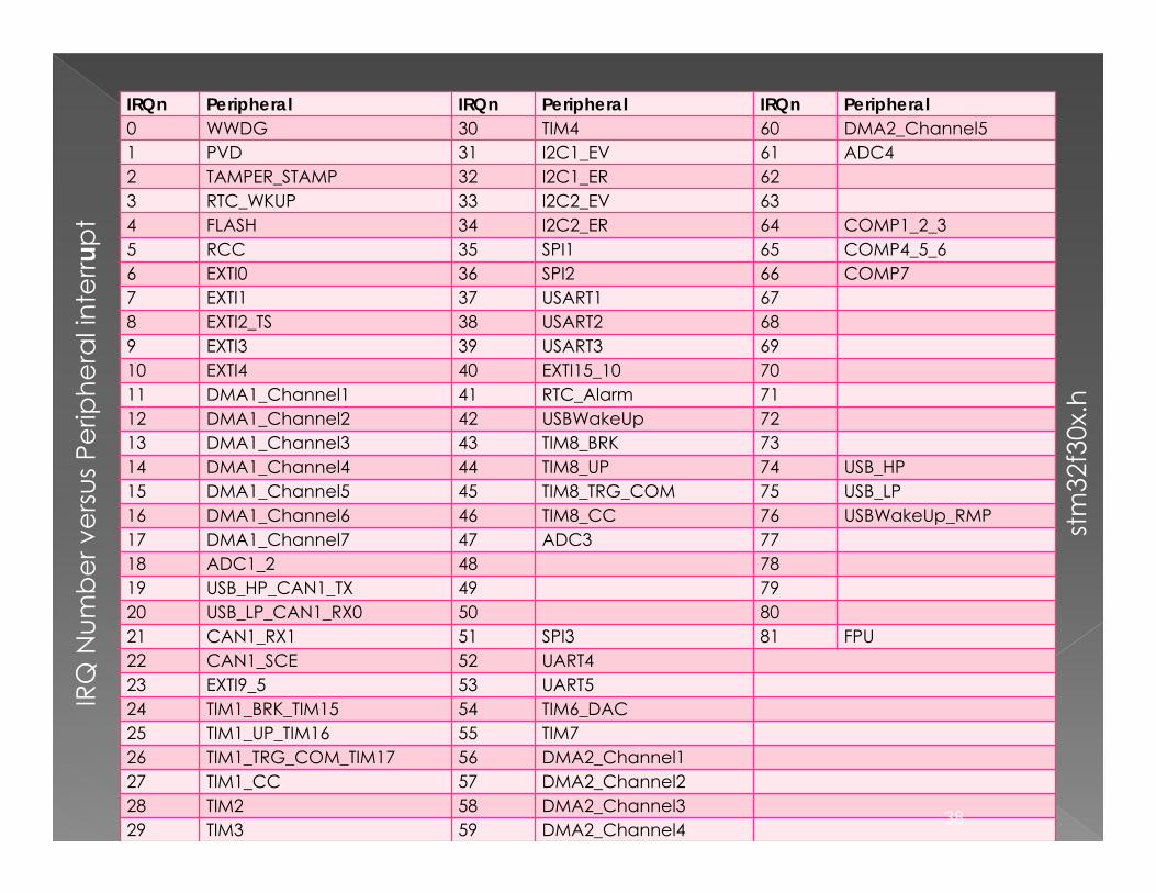
IRQn Peripheral IRQn Peripheral IRQn Peripheral0 WWDG 30 TIM4 60 DMA2_Channel5 1 PVD 31 I2C1_EV 61 ADC4 2 TAMPER_STAMP 32 I2C1_ER 62 3 RTC_WKUP 33 I2C2_EV 63 4 FLASH 34 I2C2_ER 64 COMP1_2_3 5 RCC 35 SPI1 65 COMP4_5_6 6 EXTI0 36 SPI2 66 COMP7 7 EXTI1 37 USART1 678 EXTI2_TS 38 USART2 689 EXTI3 39 USART3 6910 EXTI4 40 EXTI15_10 7011 DMA1_Channel1 41 RTC_Alarm 7112 DMA1_Channel2 42 USBWakeUp 7213 DMA1_Channel3 43 TIM8_BRK 7314 DMA1_Channel4 44 TIM8_UP 74 USB_HP 15 DMA1_Channel5 45 TIM8_TRG_COM 75 USB_LP 16 DMA1_Channel6 46 TIM8_CC 76 USBWakeUp_RMP17 DMA1_Channel7 47 ADC3 7718 ADC1_2 48 7819 USB_HP_CAN1_TX 49 7920 USB_LP_CAN1_RX0 50 8021 CAN1_RX1 51 SPI3 81 FPU22 CAN1_SCE 52 UART4 23 EXTI9_5 53 UART5 24 TIM1_BRK_TIM15 54 TIM6_DAC 25 TIM1_UP_TIM16 55 TIM7 26 TIM1_TRG_COM_TIM17 56 DMA2_Channel1 27 TIM1_CC 57 DMA2_Channel2 28 TIM2 58 DMA2_Channel3 29 TIM3 59 DMA2_Channel4
IRQ
Num
ber v
ersu
s Per
iphe
ral in
terru
pt
38
stm
32f3
0x.h
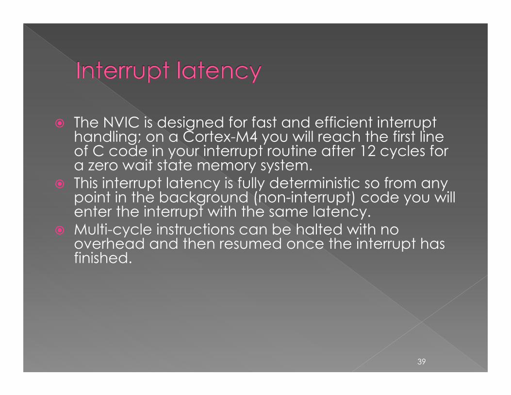
The NVIC is designed for fast and efficient interrupt handling; on a Cortex-M4 you will reach the first line of C code in your interrupt routine after 12 cycles for a zero wait state memory system. This interrupt latency is fully deterministic so from any point in the background (non-interrupt) code you will enter the interrupt with the same latency. Multi-cycle instructions can be halted with no overhead and then resumed once the interrupt has finished.
39
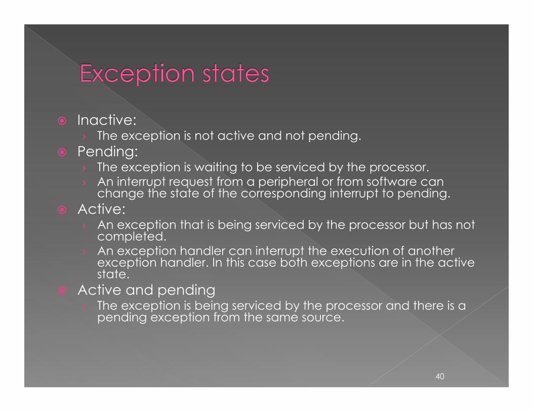
Inactive: › The exception is not active and not pending.
Pending: › The exception is waiting to be serviced by the processor.› An interrupt request from a peripheral or from software can
change the state of the corresponding interrupt to pending.Active: › An exception that is being serviced by the processor but has not
completed.› An exception handler can interrupt the execution of another
exception handler. In this case both exceptions are in the active state.
Active and pending› The exception is being serviced by the processor and there is a
pending exception from the same source.
40

Each of the USER peripherals is controlled by the IRQ register blocks. › Each user peripheral has an Interrupt Enable
bit. These bits are located across two 32-bit IRQ Set Enable registers.
› There are matching IRQ Clear Enable registers that are used to disable an interrupt source.
› The NVIC also includes pending and active registers that allow you to determine the current condition of an interrupt source.
41
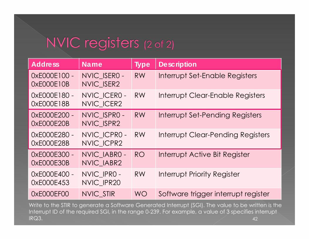
Address Name Type Description0xE000E100 -0xE000E10B
NVIC_ISER0 -NVIC_ISER2
RW Interrupt Set-Enable Registers
0xE000E180 -0xE000E18B
NVIC_ICER0 -NVIC_ICER2
RW Interrupt Clear-Enable Registers
0xE000E200 -0xE000E20B
NVIC_ISPR0 -NVIC_ISPR2
RW Interrupt Set-Pending Registers
0xE000E280 -0xE000E28B
NVIC_ICPR0 -NVIC_ICPR2
RW Interrupt Clear-Pending Registers
0xE000E300 -0xE000E30B
NVIC_IABR0 -NVIC_IABR2
RO Interrupt Active Bit Register
0xE000E400 -0xE000E453
NVIC_IPR0 -NVIC_IPR20
RW Interrupt Priority Register
0xE000EF00 NVIC_STIR WO Software trigger interrupt register
42
Write to the STIR to generate a Software Generated Interrupt (SGI). The value to be written is the Interrupt ID of the required SGI, in the range 0-239. For example, a value of 3 specifies interrupt IRQ3.
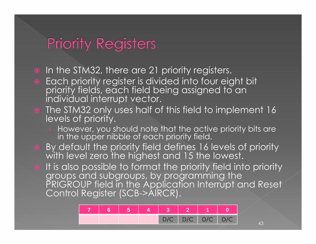
In the STM32, there are 21 priority registers. Each priority register is divided into four eight bit priority fields, each field being assigned to an individual interrupt vector. The STM32 only uses half of this field to implement 16 levels of priority. › However, you should note that the active priority bits are
in the upper nibble of each priority field. By default the priority field defines 16 levels of priority with level zero the highest and 15 the lowest. It is also possible to format the priority field into priority groups and subgroups, by programming the PRIGROUP field in the Application Interrupt and Reset Control Register (SCB->AIRCR).
7 6 5 4 3 2 1 0D/C D/C D/C D/C
43
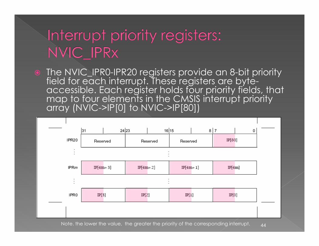
The NVIC_IPR0-IPR20 registers provide an 8-bit priority field for each interrupt. These registers are byte-accessible. Each register holds four priority fields, that map to four elements in the CMSIS interrupt priority array (NVIC->IP[0] to NVIC->IP[80])
44Note. the lower the value, the greater the priority of the corresponding interrupt.
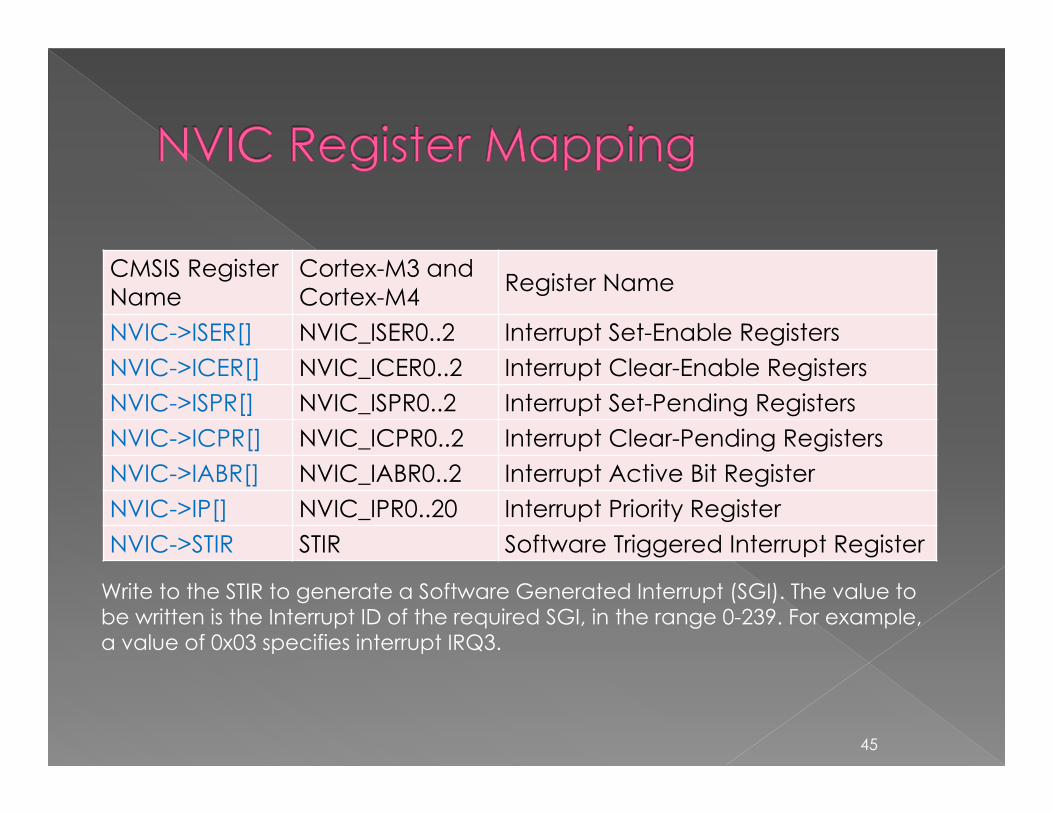
CMSIS Register Name
Cortex-M3 and Cortex-M4 Register Name
NVIC->ISER[] NVIC_ISER0..2 Interrupt Set-Enable Registers NVIC->ICER[] NVIC_ICER0..2 Interrupt Clear-Enable Registers NVIC->ISPR[] NVIC_ISPR0..2 Interrupt Set-Pending Registers NVIC->ICPR[] NVIC_ICPR0..2 Interrupt Clear-Pending Registers NVIC->IABR[] NVIC_IABR0..2 Interrupt Active Bit Register NVIC->IP[] NVIC_IPR0..20 Interrupt Priority Register NVIC->STIR STIR Software Triggered Interrupt Register
45
Write to the STIR to generate a Software Generated Interrupt (SGI). The value to be written is the Interrupt ID of the required SGI, in the range 0-239. For example, a value of 0x03 specifies interrupt IRQ3.

46
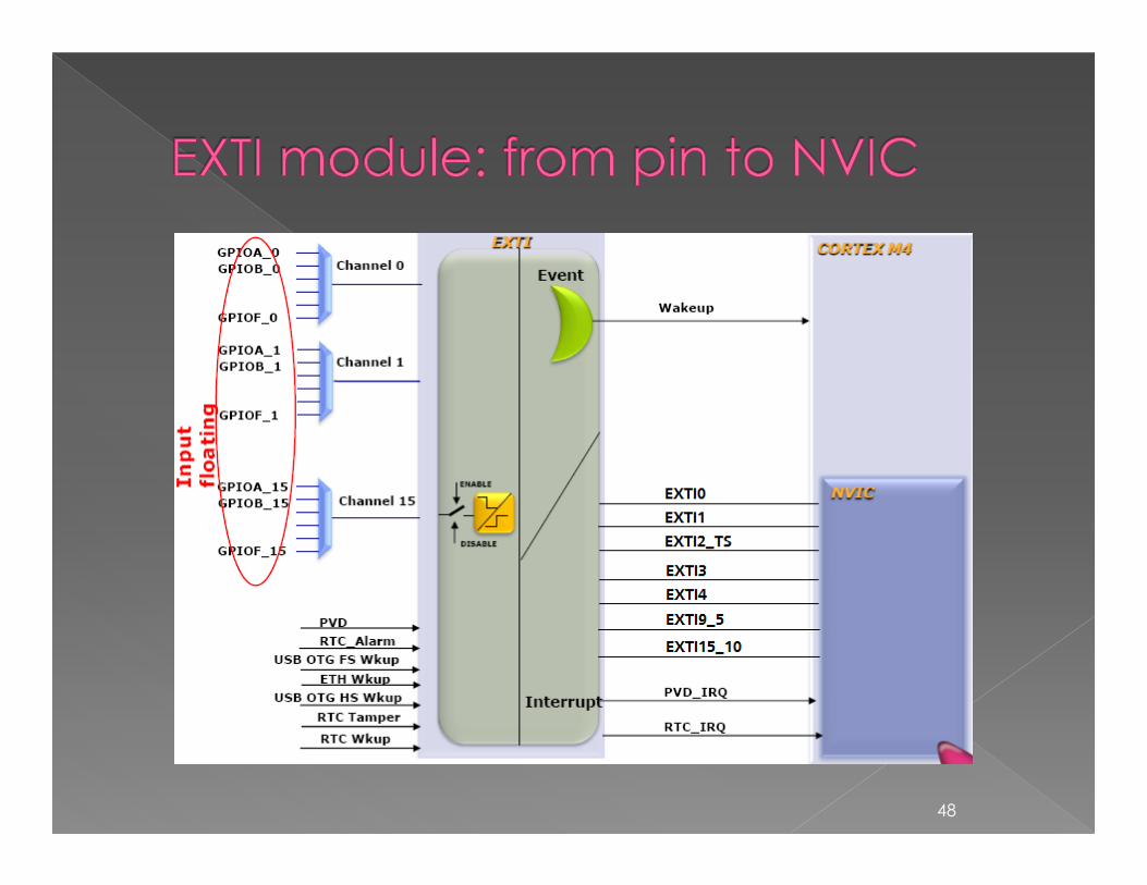
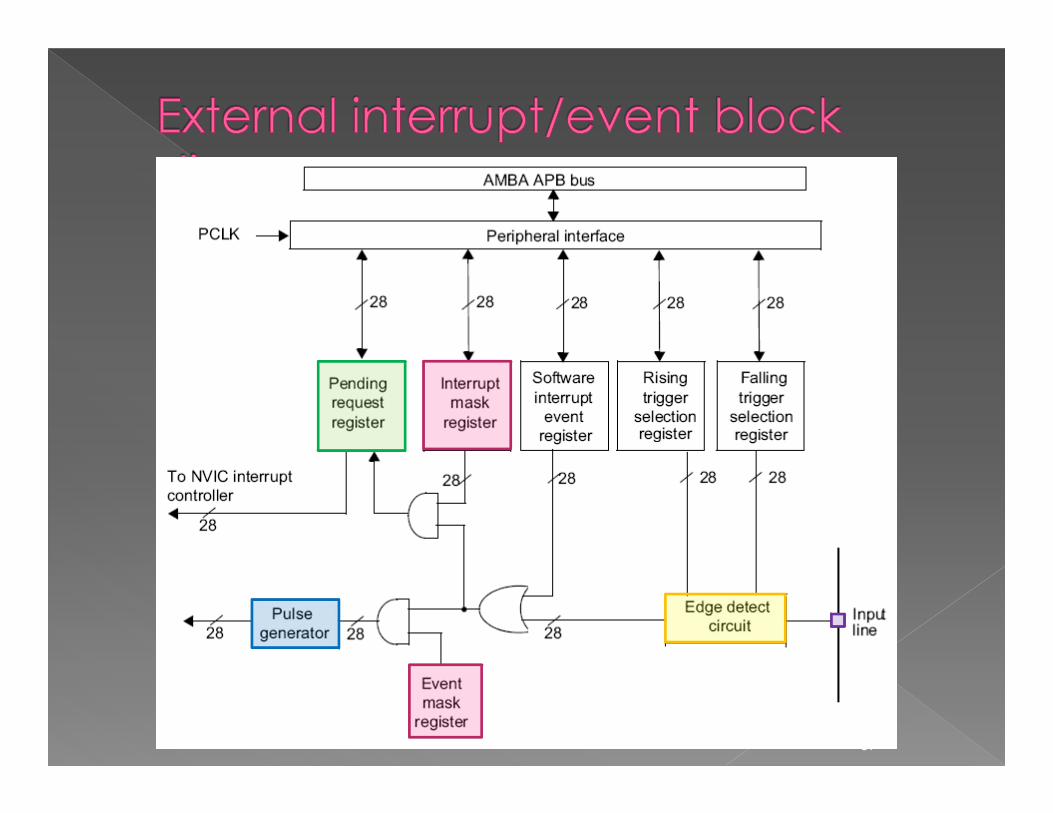
External events/interrupts are connected to NVIC through the Extended Interrupts and Events Controller (EXTI), which main features are:› support generation of up to 36 event/interrupt requests(28
external and 8 internal lines);› mapping of multiple GPIO lines to 16 NVIC external interrupt
inputs › Independent configuration of each line as an external or an
internal event request;› Independent mask on each event/interrupt line› Automatic disable of internal lines when system is not in STOP
mode› Independent trigger for external event/interrupt line› Dedicated status bit for external interrupt line;› Emulation for all the external event requests.
The STM32F30xx is able to handle external or internal events in order to wake up the core (WFE).
STM32F3 Microcontroller Reference Manual, pages 186-198 47
48
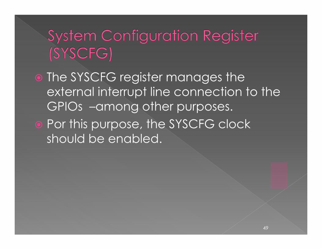
The SYSCFG register manages the external interrupt line connection to the GPIOs –among other purposes.Por this purpose, the SYSCFG clock should be enabled.
49
50
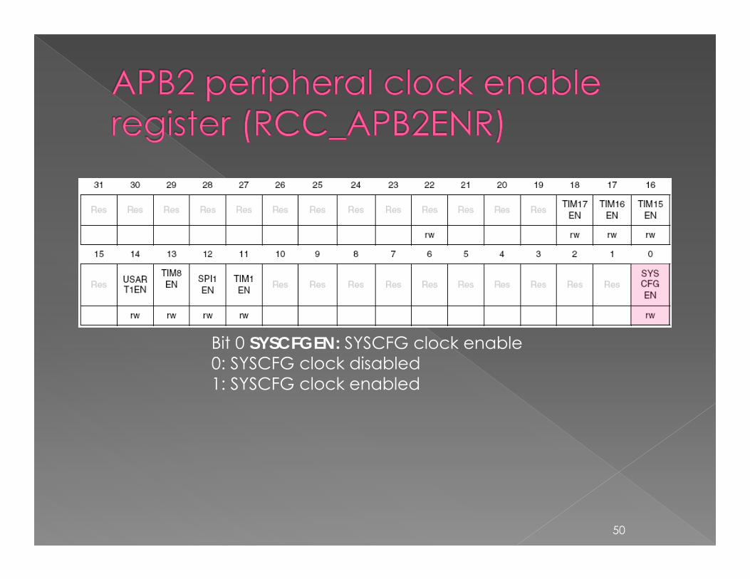
Bit 0 SYSCFGEN: SYSCFG clock enable0: SYSCFG clock disabled1: SYSCFG clock enabled
STM32F3 Microcontroller Reference Manual, pages 156-16151
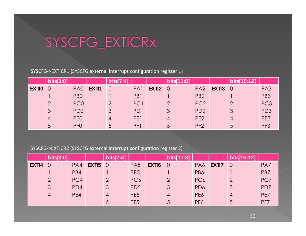
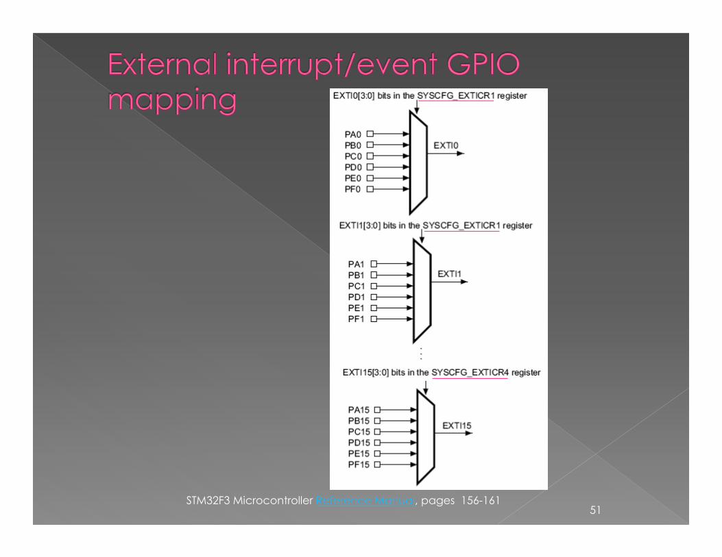
bits[3:0] bits[7:4] bits[11:8] bits[15:12]EXTI0 0
12345
PA0PB0PC0PD0PE0PF0
EXTI1 012345
PA1PB1PC1PD1PE1PF1
EXTI2 012345
PA2PB2PC2PD2PE2PF2
EXTI3 012345
PA3PB3PC3PD3PE3PF3
SYSCFG->EXTICR1 (SYSCFG external interrupt configuration register 1)
bits[3:0] bits[7:4] bits[11:8] bits[15:12]EXTI4 0
1234
PA4PB4PC4PD4PE4
EXTI5 012345
PA5PB5PC5PD5PE5PF5
EXTI6 012345
PA6PB6PC6PD6PE6PF6
EXTI7 012345
PA7PB7PC7PD7PE7PF7
SYSCFG->EXTICR2 (SYSCFG external interrupt configuration register 2)
52
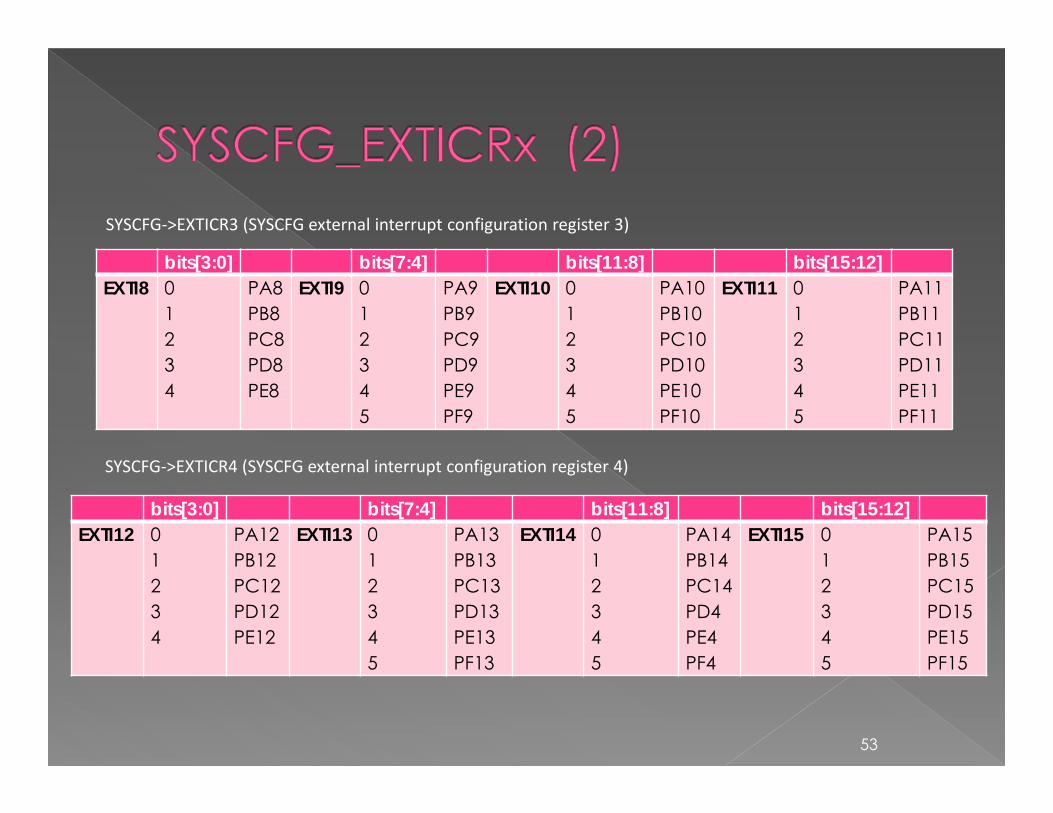
bits[3:0] bits[7:4] bits[11:8] bits[15:12]EXTI8 0
1234
PA8PB8PC8PD8PE8
EXTI9 012345
PA9PB9PC9PD9PE9PF9
EXTI10 012345
PA10PB10PC10PD10PE10PF10
EXTI11 012345
PA11PB11PC11PD11PE11PF11
SYSCFG->EXTICR3 (SYSCFG external interrupt configuration register 3)
bits[3:0] bits[7:4] bits[11:8] bits[15:12]EXTI12 0
1234
PA12PB12PC12PD12PE12
EXTI13 012345
PA13PB13PC13PD13PE13PF13
EXTI14 012345
PA14PB14PC14PD4PE4PF4
EXTI15 012345
PA15PB15PC15PD15PE15PF15
SYSCFG->EXTICR4 (SYSCFG external interrupt configuration register 4)
53

Register CMSISSYSCFG_EXTICR1 SYSCFG->EXTICR[0] SYSCFG_EXTICR2 SYSCFG->EXTICR[1]SYSCFG_EXTICR3 SYSCFG->EXTICR[2]SYSCFG_EXTICR4 SYSCFG->EXTICR[3]
54
55
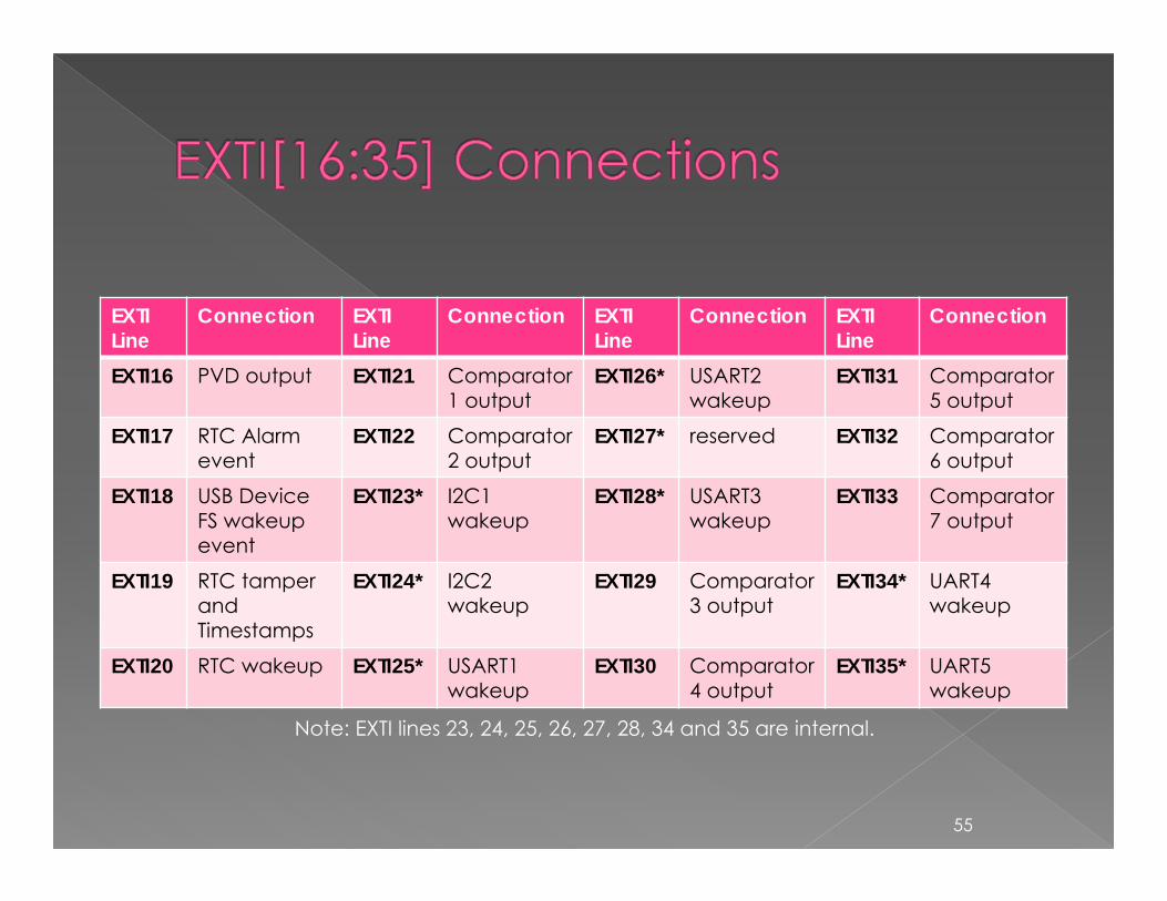
EXTILine
Connection EXTILine
Connection EXTILine
Connection EXTILine
Connection
EXTI16 PVD output EXTI21 Comparator 1 output
EXTI26* USART2 wakeup
EXTI31 Comparator 5 output
EXTI17 RTC Alarm event
EXTI22 Comparator 2 output
EXTI27* reserved EXTI32 Comparator 6 output
EXTI18 USB Device FS wakeup event
EXTI23* I2C1 wakeup
EXTI28* USART3 wakeup
EXTI33 Comparator 7 output
EXTI19 RTC tamper and Timestamps
EXTI24* I2C2 wakeup
EXTI29 Comparator 3 output
EXTI34* UART4 wakeup
EXTI20 RTC wakeup EXTI25* USART1 wakeup
EXTI30 Comparator 4 output
EXTI35* UART5 wakeup
Note: EXTI lines 23, 24, 25, 26, 27, 28, 34 and 35 are internal.
The active edge of each external interrupt line can be chosen independently, whilst for internal interrupt the active edge is always the rising one. An interrupt could be left pending› In case of an external one, a status register is instantiated
and indicates the source of the interrupt; an event is always a simple pulse and it’s used for triggering the core wake-up.
› For internal interrupts, the pending status is assured by the generating peripheral, so no need for a specific flag.
Each input line can be masked independently for interrupt or event generation, in addition the internal lines are sampled only in STOP mode. This controller allows also to emulate the (only) external events by software, multiplexed with the corresponding hardware event line, by writing to a dedicated register.
56
57
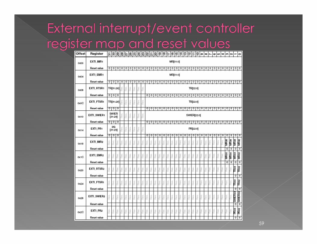
Register CMSIS Operation
Interrupt mask register
EXTI_IMR1EXTI_IMR2
EXTI->IMREXTI->IMR2
0: Interrupt request from Line x is masked1: Interrupt request from Line x is not masked
Event mask register
EXTI_EMR1EXTI_EMR2
EXTI->EMREXTI->EMR2
0: Event request from Line x is masked1: Event request from Line x is not masked
Rising trigger selection register
EXTI_RTSR1EXTI_RTSR2
EXTI->RTSREXTI->RTSR2
0: Rising trigger disabled (for Event and Interrupt) for input line1: Rising trigger enabled (for Event and Interrupt) for input line.
Falling trigger selection register
EXTI_FTSR1EXTI_FTSR2
EXTI->FTSREXTI->FTSR2
0: Falling trigger disabled (for Event and Interrupt) for input line1: Falling trigger enabled (for Event and Interrupt) for input line.
Software interrupt event register
EXTI_SWIER1EXTI_SWIER2
EXTI->SWIEREXTI->SWIER2
Writing a ‘1’ to this bit when it is at ‘0’ sets the corresponding pending bit in the EXTI_PR register. If the interrupt is enabled on this line on the EXTI_IMR and EXTI_EMR registers, an interrupt request is generated. This bit is cleared by writing a ‘1’ into the corresponding bit in the EXTI_PR register .
Pending register EXTI_PR1EXTI_PR2
EXTI->PREXTI->PR2
0: No trigger request occurred1: Selected trigger request occurredThis bit is set when the selected edge event arrives on the external interrupt line. This bit is cleared by writing a ‘1’ to the bit or by changing the sensitivity of the edge detector.
58
Two configuration modes:• Interrupt mode: generate interrupts with external lines edges• Event mode: generate pulse to wake-up system from SLEEP and STOP modes
59
To configure an external interrupt one must configure the external interrupt (EXTI) peripheral as well as the NVIC peripheral. The general procedure is as follows:› Configure the EXTIxx bits in the SYSCFG_EXTICRx
registers to map the GPIO pin(s) of interest to the appropriate external interrupt lines (EXTI0-EXTI15).
› For the external interrupt lines (EXTIxx) of interest, choose a signal change that will trigger the external interrupt. The signal change can be a rising edge, a falling edge or both. These can be set via the EXTI_RTSR (rising) and the EXTI_FTSR (falling) registers.
› Unmask the external interrupt line(s) of interest. by setting the bit corresponding to the EXTI line of interest in the EXTI_IMR register.
60
› Set the priority for the interrupt vector in question in the NVIC either via the CMSIS based “NVIC_SetPriority()” function or through the IPR0-IPR7 registers.
› Enable the interrupt in the NVIC either via the CMSIS based “NVIC_EnableIRQ()” function or via the ISER register.
› Write your interrupt service routine (ISR).› Inside your interrupt service routine, check the source
of the interrupt…either the GPIO pin directly or the external interrupt line. Once you figure out which one triggered the interrupt, perform the interrupt processing scheme associated with it. Make sure that you clear the corresponding pending bit of the external interrupt lines of interest in the EXTI_PR (external interrupt pending register) register by writing a ’1′ to it.
61
# Action Registers to be modified1 Enable GPIOx clock RCC->AHBENR.IOPxEN
2 Configure the GPIOx pin as floating input GPIOx->MODER.MODERyGPIOx->PUPDR.PUPDRy
3 Enable SYSCFG clock RCC->APB2ENR.SYSCFGEN
4 Select the GPIOx pin as input for the interrupt line INTIy
SYSCFG->EXTICR[z]
5 Unmask INTy EXTI_IMRx
5 Select the edge or edges that could trigger the interrupt
EXTI_RTSRxEXTI_FTSRx
6 Enable the interrupt line NVIC->ISER[z]
7 Select the priority and subpriority of the interrupt
SCB->AIRCR.PRIGROUPNVIC->IP[y]
62

63
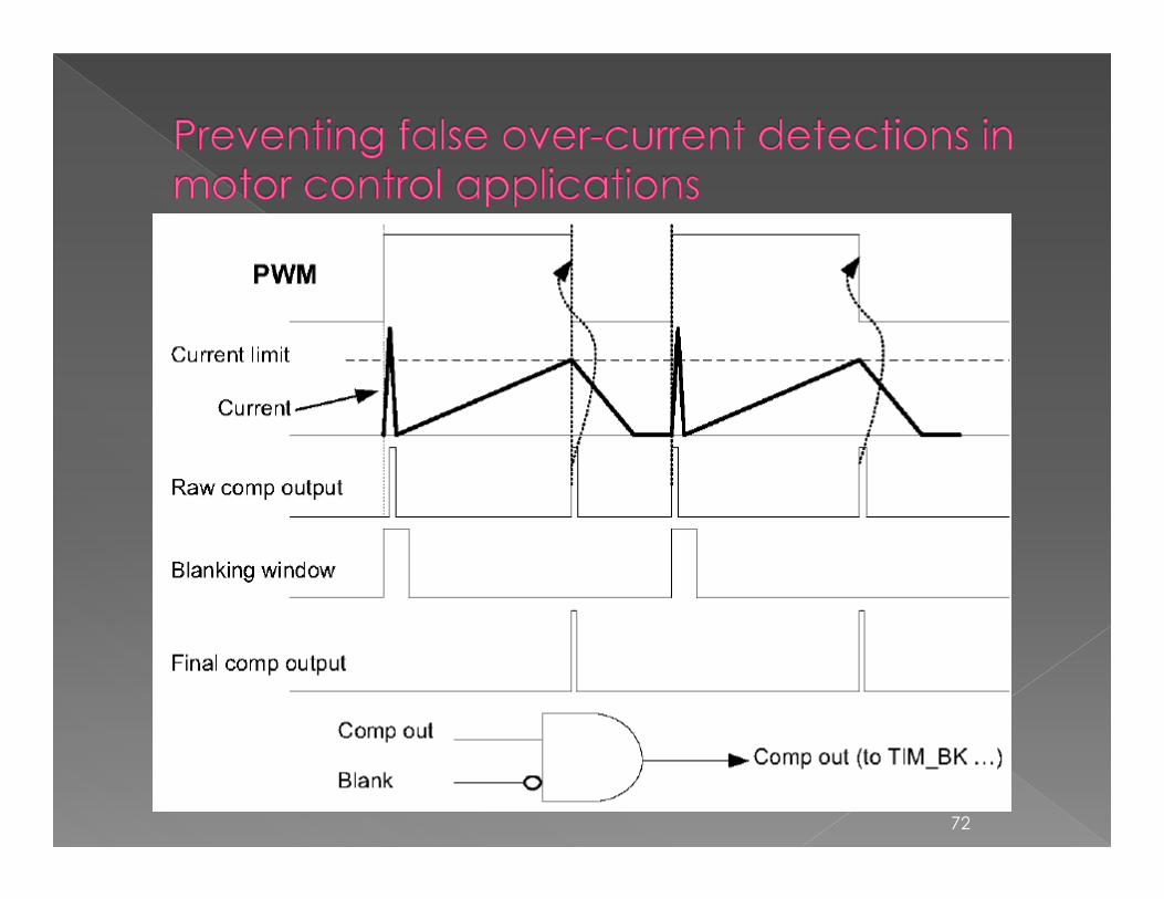
STM32F3 Microcontroller Reference Manual, pages 324-344
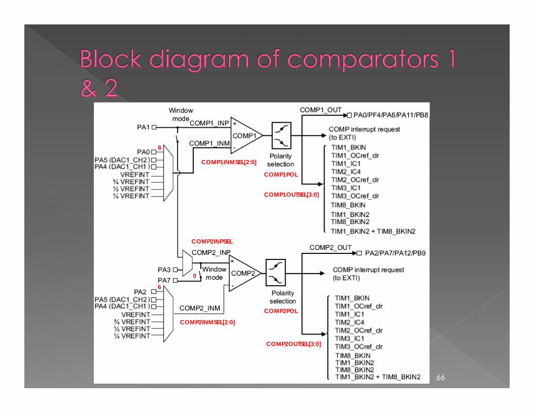
The STM32F30xxx embeds seven general purpose comparators that can be used either as standalone devices (all terminal are available on I/Os) or combined with the timers.They can be used for a variety of functions including:› wake-up from low-power mode triggered by an analog signal;› analog signal conditioning; › cycle-by-cycle current control loop when combined with the
DAC and a PWM output from a timer.) Rail-to-rail comparatorsEach comparator has configurable positive and negative inputs used for flexible voltage selection:› Multiplexed I/O pins› DAC channel 1 or DAC channel 2› Internal reference voltage and three submultiple values (1/4, 1/2,
3/4) provided by scaler (buffered voltage divider).
64

Programmable hysteresisProgrammable speed and consumptionThe outputs can be redirected to an I/O or to multiple timer inputs for triggering:› Capture events› OCref_clr events (for cycle-by-cycle current control)› Break events for fast PWM shutdowns
COMP1 and COMP2, COMP3/COMP4, and COMP5/COMP6 comparators can be combined in a window comparator. COMP7 does not support the window mode.Comparators output with blanking sourceEach comparator has interrupt generation capability with wake-up from Sleep and Stop modes (through the EXTI controller)
65
66
COMP1INMSEL[2:0]
COMP1POL
COMP1OUTSEL[3:0]
COMP2INPSEL
COMP2INMSEL[2:0]
COMP2OUTSEL[3:0]
COMP2POL
6
6
0
The COMP clock provided by the clock controller is synchronous with the PCLK2 (APB2 clock).There is no clock enable control bit provided in the RCC controller. To use a clock source for the comparator, the SYSCFG clock enable control bit must be set in the RCC controller.Note: The polarity selection logic and the output redirection to the port works independently from the PCLK2 clock. This allows the comparator to work even in Stop mode.
67
The I/Os used as comparators inputs must be configured in analog mode in the GPIOs registers.The comparator output can be connected to the I/Os using the alternate function channel given in “Alternate function mapping” table in the datasheet.The output can also be internally redirected to a variety of timer input for the following purposes:› Emergency shut-down of PWM signals, using BKIN and
BKIN2 inputs› Cycle-by-cycle current control, using OCref_clr inputs› Input capture for timing measures
It is possible to have the comparator output simultaneously redirected internally and externally.
68
The comparator outputs are internally connected to the Extended interrupts and events controller (EXTI). Each comparator has its own EXTI line and can generate either interrupts or events. The same mechanism is used to exit from low power modes.
Power modeThe comparator power consumption versus propagation delay can be adjusted to have the optimum trade-off for a given application using the bits COMPxMODE[1:0] in COMPx_CSRregisters
69
70
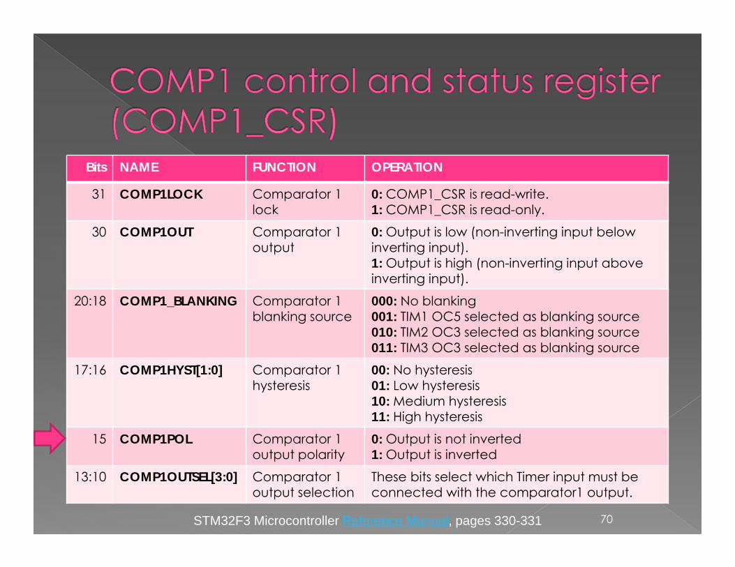
Bits NAME FUNCTION OPERATION
31 COMP1LOCK Comparator 1 lock
0: COMP1_CSR is read-write.1: COMP1_CSR is read-only.
30 COMP1OUT Comparator 1 output
0: Output is low (non-inverting input below inverting input).1: Output is high (non-inverting input above inverting input).
20:18 COMP1_BLANKING Comparator 1 blanking source
000: No blanking001: TIM1 OC5 selected as blanking source010: TIM2 OC3 selected as blanking source011: TIM3 OC3 selected as blanking source
17:16 COMP1HYST[1:0] Comparator 1 hysteresis
00: No hysteresis01: Low hysteresis10: Medium hysteresis11: High hysteresis
15 COMP1POL Comparator 1 output polarity
0: Output is not inverted1: Output is inverted
13:10 COMP1OUTSEL[3:0] Comparator 1 output selection
These bits select which Timer input must be connected with the comparator1 output.
STM32F3 Microcontroller Reference Manual, pages 330-331
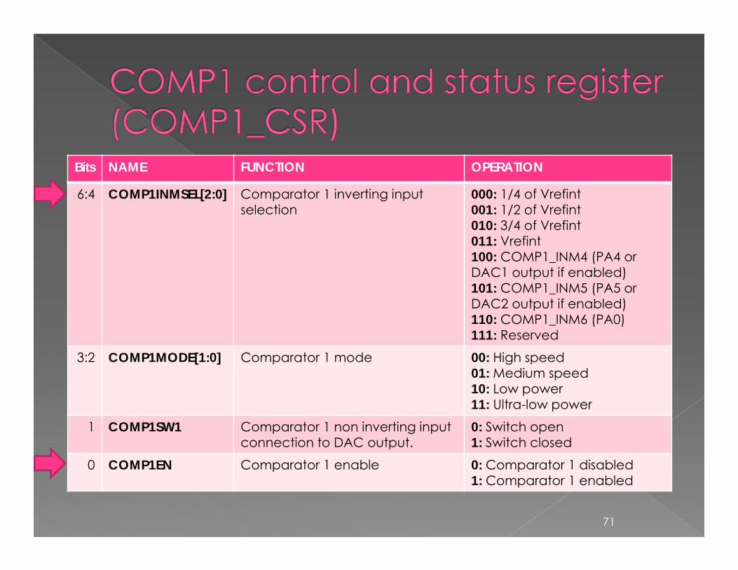
Bits NAME FUNCTION OPERATION
6:4 COMP1INMSEL[2:0] Comparator 1 inverting input selection
000: 1/4 of Vrefint001: 1/2 of Vrefint010: 3/4 of Vrefint011: Vrefint100: COMP1_INM4 (PA4 or DAC1 output if enabled)101: COMP1_INM5 (PA5 or DAC2 output if enabled)110: COMP1_INM6 (PA0)111: Reserved
3:2 COMP1MODE[1:0] Comparator 1 mode 00: High speed01: Medium speed10: Low power11: Ultra-low power
1 COMP1SW1 Comparator 1 non inverting input connection to DAC output.
0: Switch open1: Switch closed
0 COMP1EN Comparator 1 enable 0: Comparator 1 disabled1: Comparator 1 enabled
71
72