Embed Size (px)
Citation preview
9/28/03 Brainerd/photoclass/ECE580/Optics/Optic3_NA_s
1
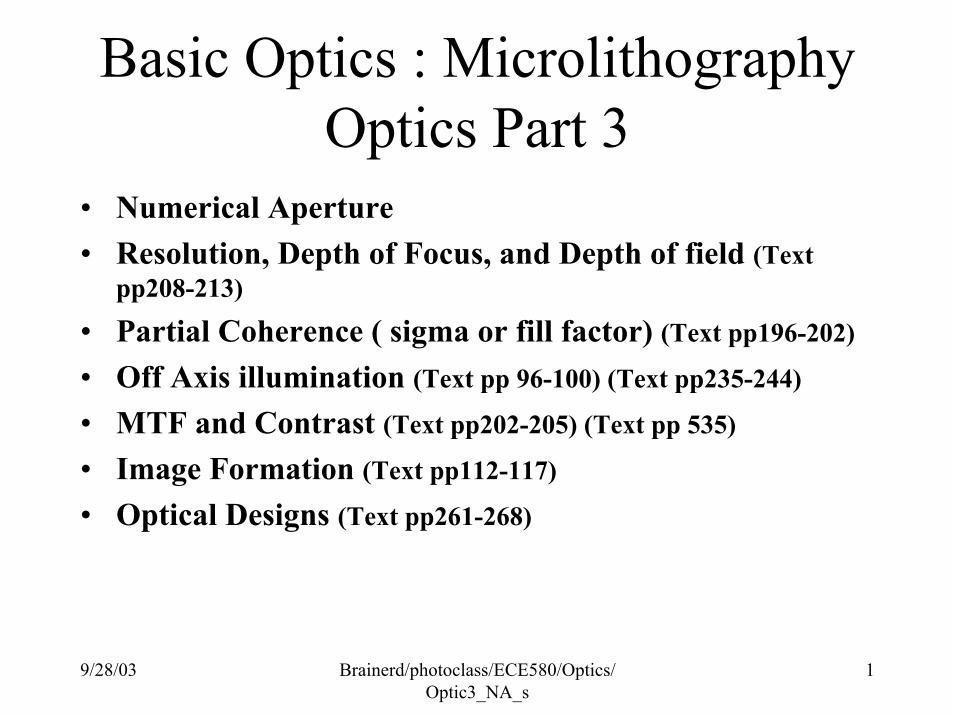
Basic Optics : MicrolithographyOptics Part 3
• Numerical Aperture• Resolution, Depth of Focus, and Depth of field (Text
pp208-213)
• Partial Coherence ( sigma or fill factor) (Text pp196-202)
• Off Axis illumination (Text pp 96-100) (Text pp235-244)
• MTF and Contrast (Text pp202-205) (Text pp 535)
• Image Formation (Text pp112-117)
• Optical Designs (Text pp261-268)
9/28/03 Brainerd/photoclass/ECE580/Optics/Optic3_NA_s
2
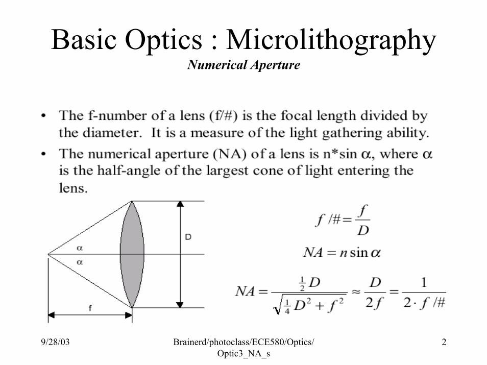
Basic Optics : MicrolithographyNumerical Aperture
9/28/03 Brainerd/photoclass/ECE580/Optics/Optic3_NA_s
3
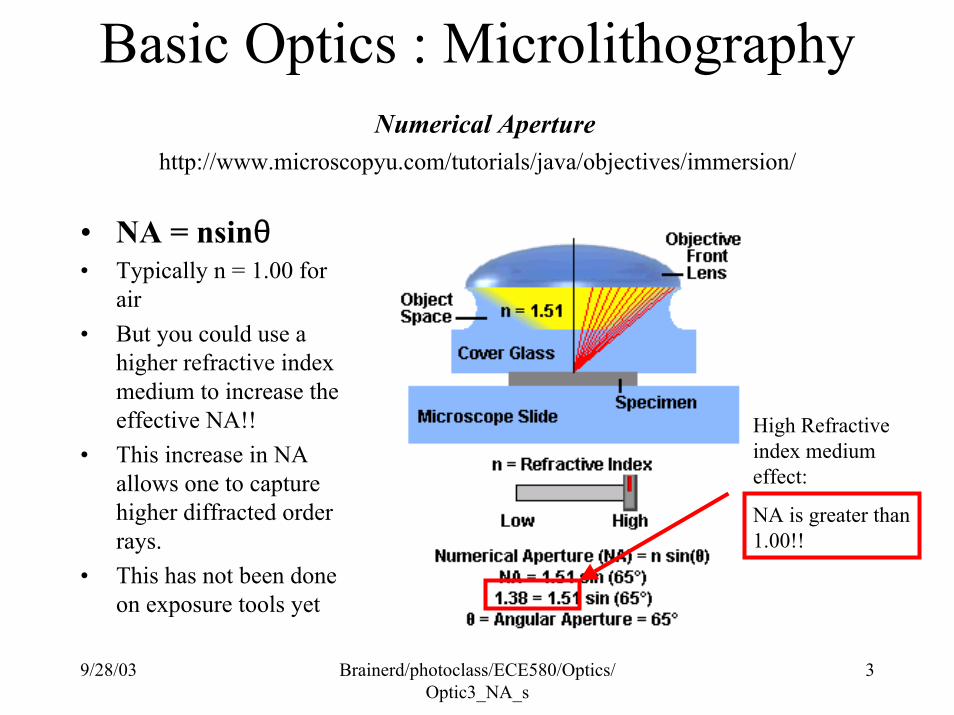
Basic Optics : MicrolithographyNumerical Aperture
http://www.microscopyu.com/tutorials/java/objectives/immersion/
• NA = nsinθ• Typically n = 1.00 for
air• But you could use a
higher refractive index medium to increase the effective NA!!
• This increase in NA allows one to capture higher diffracted order rays.
• This has not been done on exposure tools yet
High Refractive index medium effect:
NA is greater than 1.00!!
9/28/03 Brainerd/photoclass/ECE580/Optics/Optic3_NA_s
4
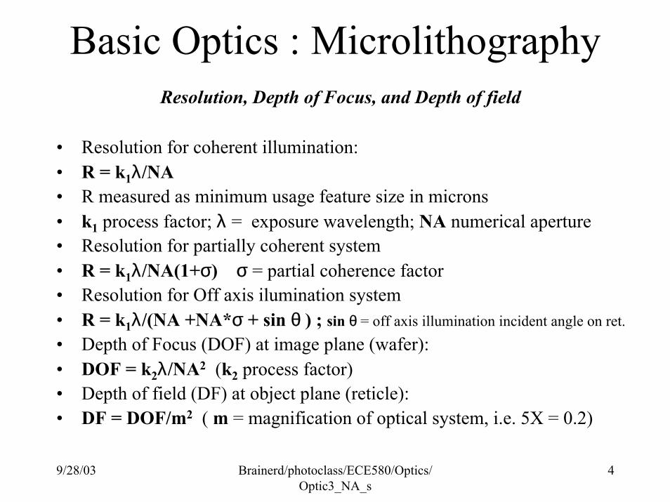
Basic Optics : MicrolithographyResolution, Depth of Focus, and Depth of field
• Resolution for coherent illumination:• R = k1λ/NA• R measured as minimum usage feature size in microns• k1 process factor; λ = exposure wavelength; NA numerical aperture• Resolution for partially coherent system• R = k1λ/NA(1+σ) σ = partial coherence factor• Resolution for Off axis ilumination system• R = k1λ/(NA +NA*σ + sin θ ) ; sin θ = off axis illumination incident angle on ret.• Depth of Focus (DOF) at image plane (wafer):• DOF = k2λ/NA2 (k2 process factor)• Depth of field (DF) at object plane (reticle):• DF = DOF/m2 ( m = magnification of optical system, i.e. 5X = 0.2)
9/28/03 Brainerd/photoclass/ECE580/Optics/Optic3_NA_s
5
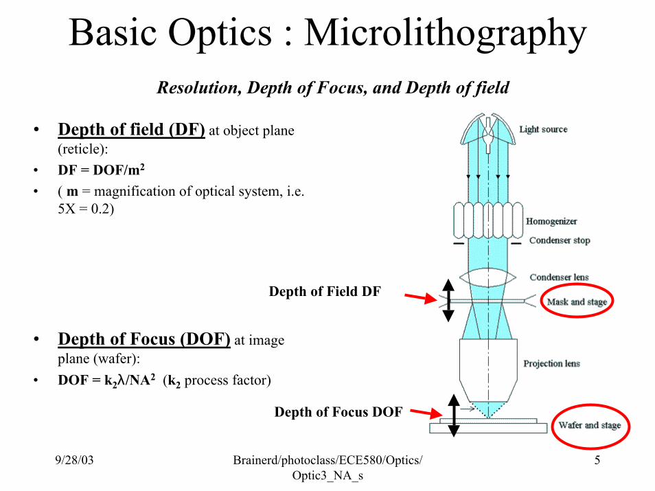
Basic Optics : MicrolithographyResolution, Depth of Focus, and Depth of field
• Depth of field (DF) at object plane (reticle):
• DF = DOF/m2
• ( m = magnification of optical system, i.e. 5X = 0.2)
• Depth of Focus (DOF) at image plane (wafer):
• DOF = k2λ/NA2 (k2 process factor)
Depth of Field DF
Depth of Focus DOF
9/28/03 Brainerd/photoclass/ECE580/Optics/Optic3_NA_s
6
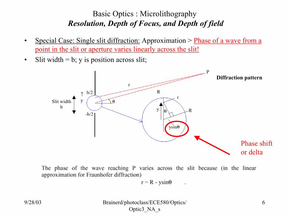
Basic Optics : MicrolithographyResolution, Depth of Focus, and Depth of field
• Special Case: Single slit diffraction: Approximation > Phase of a wave from a point in the slit or aperture varies linearly across the slit!
• Slit width = b; y is position across slit;
Diffraction pattern
Phase shift or delta
9/28/03 Brainerd/photoclass/ECE580/Optics/Optic3_NA_s
7
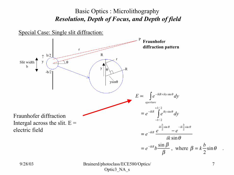
Basic Optics : MicrolithographyResolution, Depth of Focus, and Depth of field
Special Case: Single slit diffraction:Fraunhoferdiffraction pattern
Fraunhofer diffractionIntergal across the slit. E = electric field
9/28/03 Brainerd/photoclass/ECE580/Optics/Optic3_NA_s
8
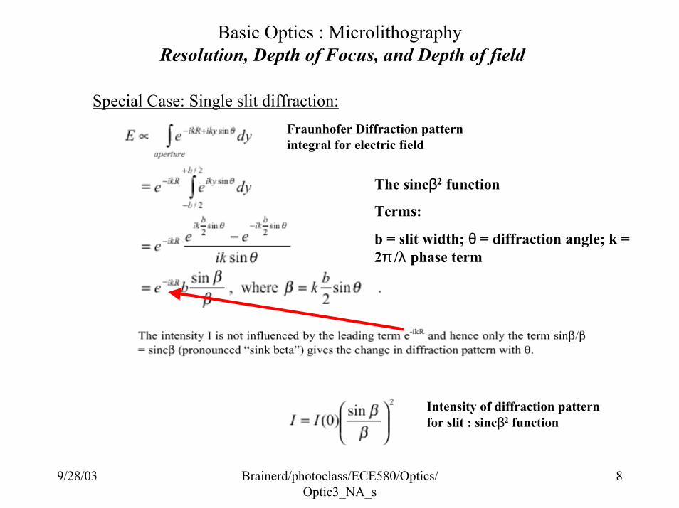
Basic Optics : MicrolithographyResolution, Depth of Focus, and Depth of field
Special Case: Single slit diffraction:
The sincβ2 function
Terms:
b = slit width; θ = diffraction angle; k = 2π /λ phase term
Fraunhofer Diffraction pattern integral for electric field
Intensity of diffraction pattern for slit : sincβ2 function
9/28/03 Brainerd/photoclass/ECE580/Optics/Optic3_NA_s
9
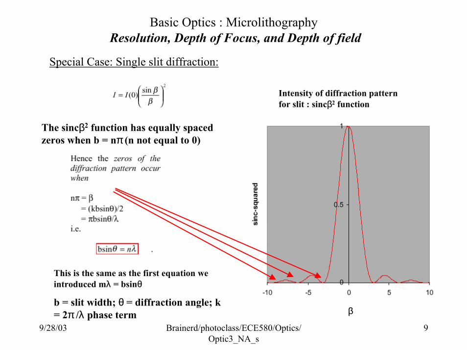
Basic Optics : MicrolithographyResolution, Depth of Focus, and Depth of field
Special Case: Single slit diffraction:
This is the same as the first equation we introduced mλ = bsinθ
b = slit width; θ = diffraction angle; k = 2π /λ phase term
The sincβ2 function has equally spaced zeros when b = nπ (n not equal to 0)
Intensity of diffraction pattern for slit : sincβ2 function
β
9/28/03 Brainerd/photoclass/ECE580/Optics/Optic3_NA_s
10
Basic Optics : MicrolithographyResolution, Depth of Focus, and Depth of field
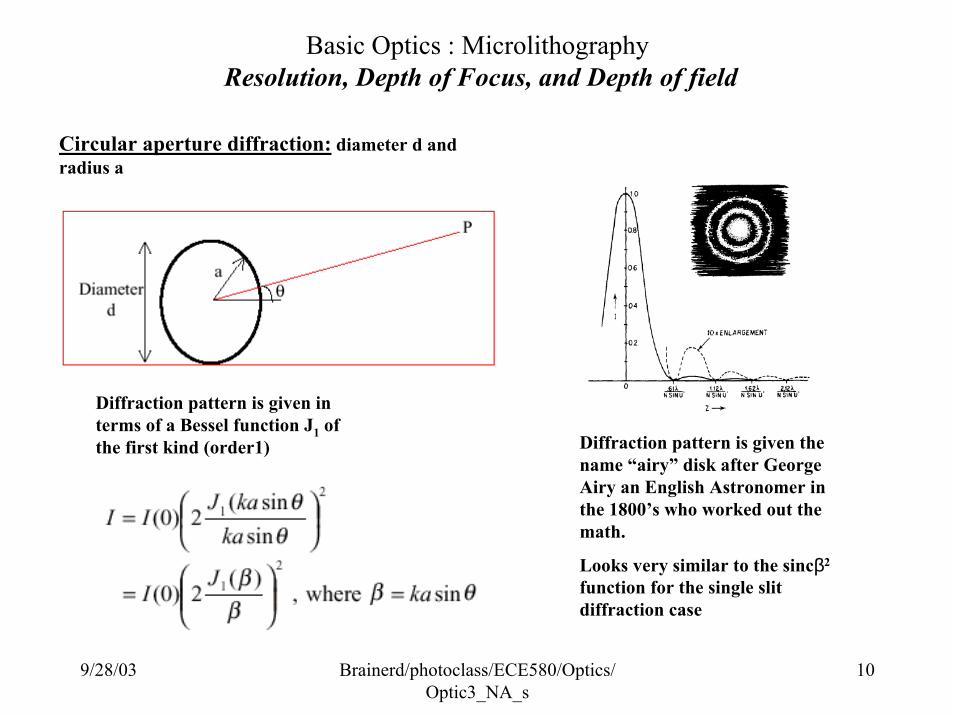
Circular aperture diffraction: diameter d and radius a
Diffraction pattern is given in terms of a Bessel function J1 of the first kind (order1) Diffraction pattern is given the
name “airy” disk after George Airy an English Astronomer in the 1800’s who worked out the math.
Looks very similar to the sincβ2
function for the single slit diffraction case
9/28/03 Brainerd/photoclass/ECE580/Optics/Optic3_NA_s
11
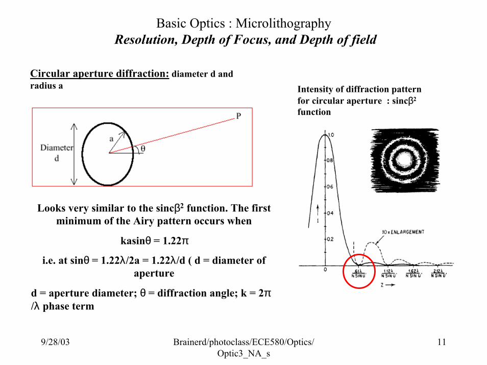
Basic Optics : MicrolithographyResolution, Depth of Focus, and Depth of field
Circular aperture diffraction: diameter d and radius a Intensity of diffraction pattern
for circular aperture : sincβ2
function
Looks very similar to the sincβ2 function. The first minimum of the Airy pattern occurs when
kasinθ = 1.22π
i.e. at sinθ = 1.22λ/2a = 1.22λ/d ( d = diameter of aperture
d = aperture diameter; θ = diffraction angle; k = 2π/λ phase term
9/28/03 Brainerd/photoclass/ECE580/Optics/Optic3_NA_s
12
Basic Optics : MicrolithographyResolution, Depth of Focus, and Depth of field
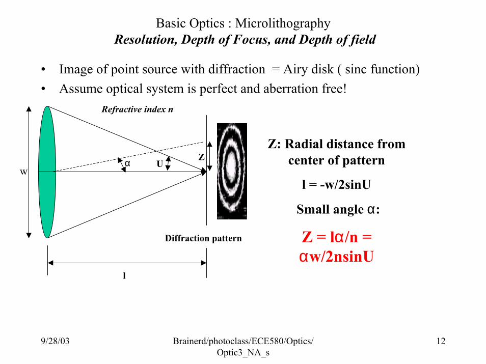
• Image of point source with diffraction = Airy disk ( sinc function)• Assume optical system is perfect and aberration free!
w
Diffraction pattern
l
Z
Refractive index n
Uα
Z: Radial distance from center of pattern
l = -w/2sinU
Small angle α:
Z = lα/n = αw/2nsinU
9/28/03 Brainerd/photoclass/ECE580/Optics/Optic3_NA_s
13
Basic Optics : MicrolithographyResolution, Depth of Focus, and Depth of field
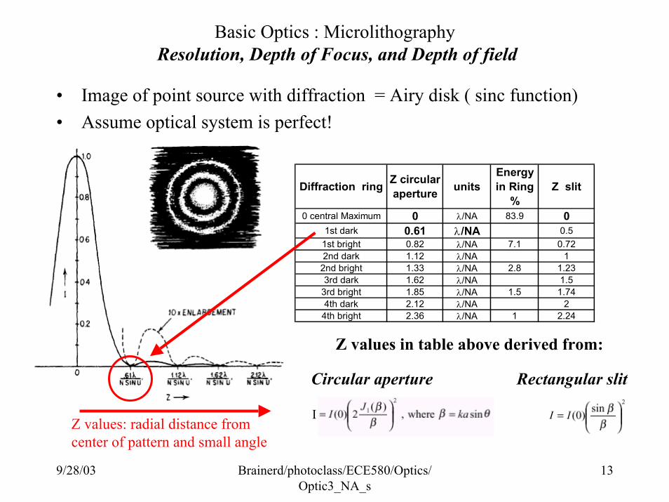
• Image of point source with diffraction = Airy disk ( sinc function)• Assume optical system is perfect!
Z values: radial distance from center of pattern and small angle
Diffraction ring Z circular aperture units
Energy in Ring
%Z slit
0 central Maximum 0 λ/NA 83.9 01st dark 0.61 λ/NA 0.5
1st bright 0.82 λ/NA 7.1 0.722nd dark 1.12 λ/NA 1
2nd bright 1.33 λ/NA 2.8 1.233rd dark 1.62 λ/NA 1.5
3rd bright 1.85 λ/NA 1.5 1.744th dark 2.12 λ/NA 2
4th bright 2.36 λ/NA 1 2.24
I
Circular aperture Rectangular slit
Z values in table above derived from:
9/28/03 Brainerd/photoclass/ECE580/Optics/Optic3_NA_s
14
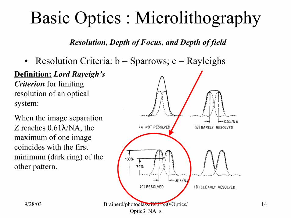
Basic Optics : MicrolithographyResolution, Depth of Focus, and Depth of field
• Resolution Criteria: b = Sparrows; c = RayleighsDefinition: Lord Rayeigh’sCriterion for limiting resolution of an optical system:
When the image separation Z reaches 0.61λ/NA, the maximum of one image coincides with the first minimum (dark ring) of the other pattern.
9/28/03 Brainerd/photoclass/ECE580/Optics/Optic3_NA_s
15
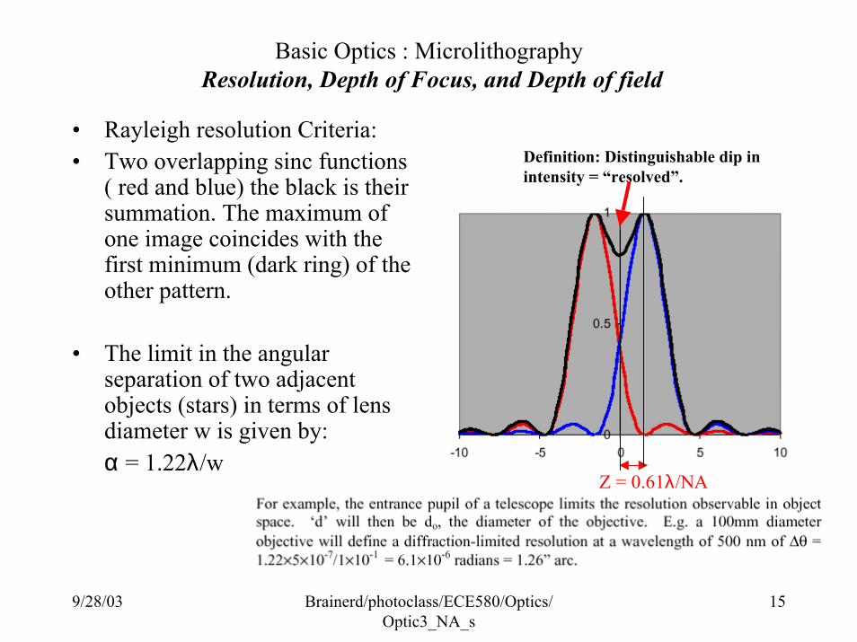
Basic Optics : MicrolithographyResolution, Depth of Focus, and Depth of field
• Rayleigh resolution Criteria:• Two overlapping sinc functions
( red and blue) the black is their summation. The maximum of one image coincides with the first minimum (dark ring) of the other pattern.
• The limit in the angular separation of two adjacent objects (stars) in terms of lens diameter w is given by:α = 1.22λ/w
Definition: Distinguishable dip in intensity = “resolved”.
Z = 0.61λ/NA
9/28/03 Brainerd/photoclass/ECE580/Optics/Optic3_NA_s
16
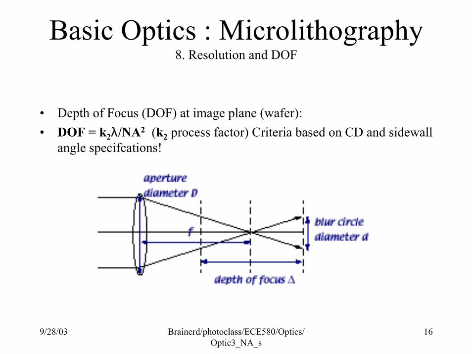
Basic Optics : Microlithography8. Resolution and DOF
• Depth of Focus (DOF) at image plane (wafer):• DOF = k2λ/NA2 (k2 process factor) Criteria based on CD and sidewall
angle specifcations!
9/28/03 Brainerd/photoclass/ECE580/Optics/Optic3_NA_s
17
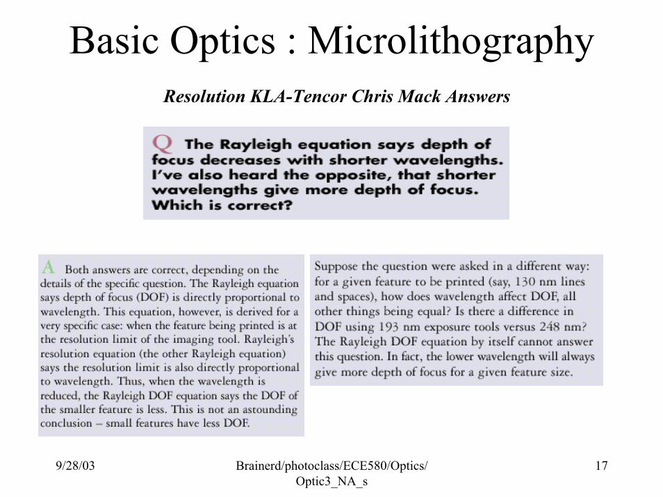
Basic Optics : MicrolithographyResolution KLA-Tencor Chris Mack Answers
9/28/03 Brainerd/photoclass/ECE580/Optics/Optic3_NA_s
18
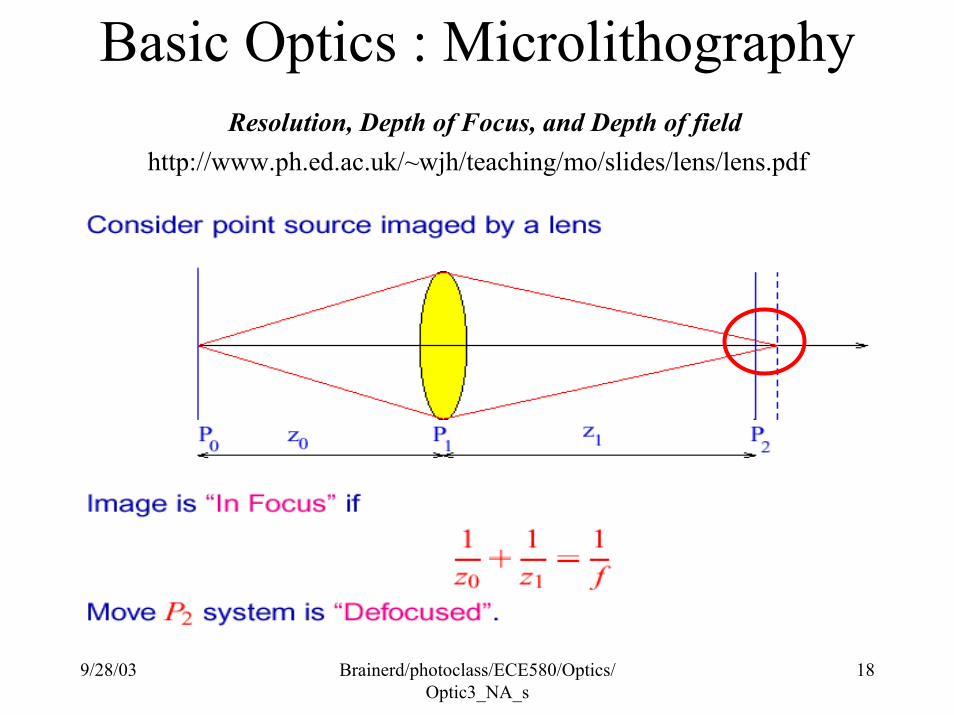
Basic Optics : MicrolithographyResolution, Depth of Focus, and Depth of field
http://www.ph.ed.ac.uk/~wjh/teaching/mo/slides/lens/lens.pdf
9/28/03 Brainerd/photoclass/ECE580/Optics/Optic3_NA_s
19
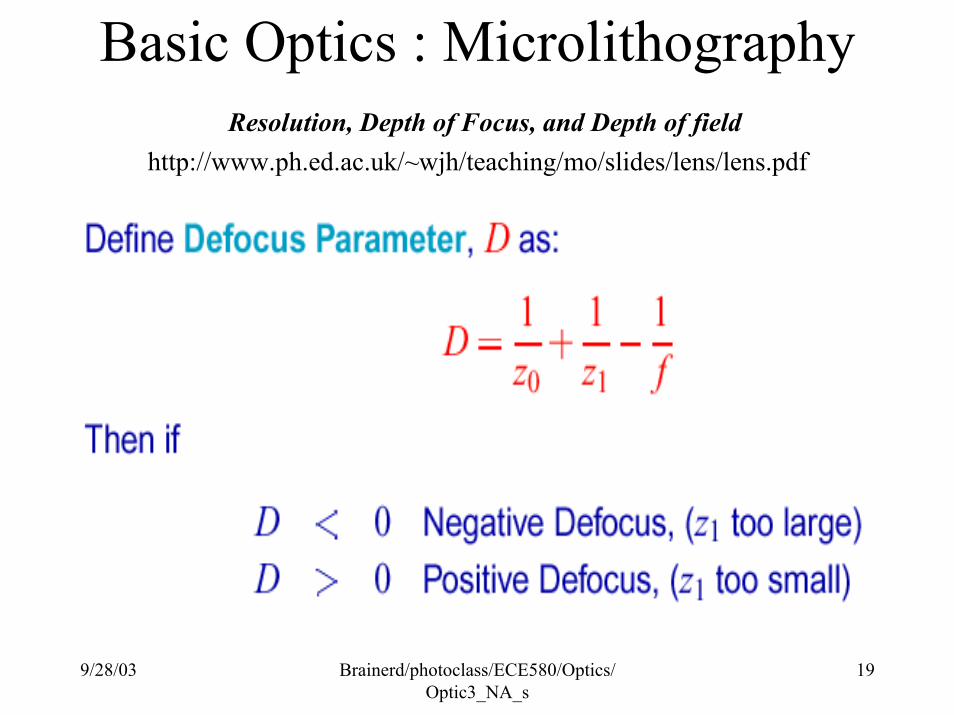
Basic Optics : MicrolithographyResolution, Depth of Focus, and Depth of field
http://www.ph.ed.ac.uk/~wjh/teaching/mo/slides/lens/lens.pdf
9/28/03 Brainerd/photoclass/ECE580/Optics/Optic3_NA_s
20
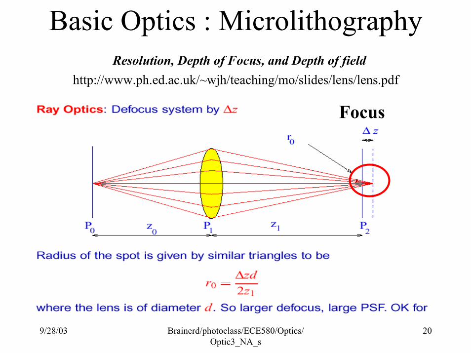
Basic Optics : MicrolithographyResolution, Depth of Focus, and Depth of field
http://www.ph.ed.ac.uk/~wjh/teaching/mo/slides/lens/lens.pdf
Focus
9/28/03 Brainerd/photoclass/ECE580/Optics/Optic3_NA_s
21
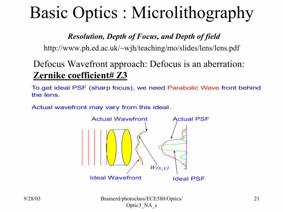
Basic Optics : MicrolithographyResolution, Depth of Focus, and Depth of field
http://www.ph.ed.ac.uk/~wjh/teaching/mo/slides/lens/lens.pdf
Defocus Wavefront approach: Defocus is an aberration:Zernike coefficient# Z3
9/28/03 Brainerd/photoclass/ECE580/Optics/Optic3_NA_s
22
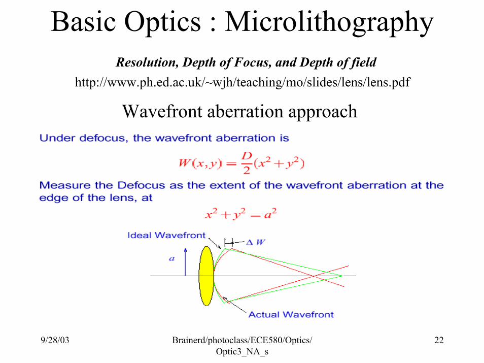
Basic Optics : MicrolithographyResolution, Depth of Focus, and Depth of field
http://www.ph.ed.ac.uk/~wjh/teaching/mo/slides/lens/lens.pdf
Wavefront aberration approach
9/28/03 Brainerd/photoclass/ECE580/Optics/Optic3_NA_s
23
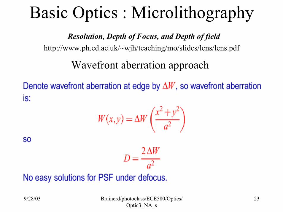
Basic Optics : MicrolithographyResolution, Depth of Focus, and Depth of field
http://www.ph.ed.ac.uk/~wjh/teaching/mo/slides/lens/lens.pdf
Wavefront aberration approach
9/28/03 Brainerd/photoclass/ECE580/Optics/Optic3_NA_s
24
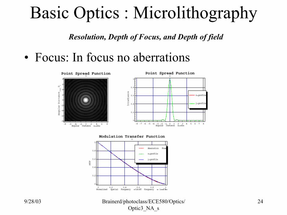
Basic Optics : MicrolithographyResolution, Depth of Focus, and Depth of field
• Focus: In focus no aberrations
9/28/03 Brainerd/photoclass/ECE580/Optics/Optic3_NA_s
25
Basic Optics : MicrolithographyResolution, Depth of Focus, and Depth of field
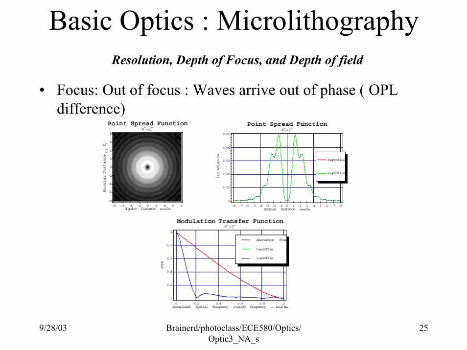
• Focus: Out of focus : Waves arrive out of phase ( OPL difference)
9/28/03 Brainerd/photoclass/ECE580/Optics/Optic3_NA_s
26
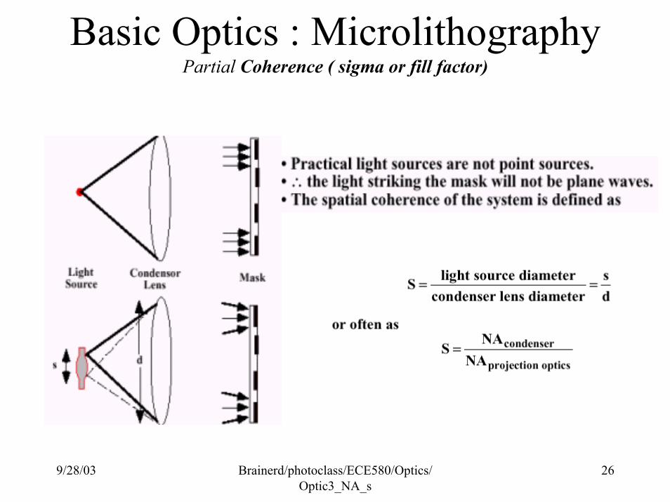
Basic Optics : MicrolithographyPartial Coherence ( sigma or fill factor)
9/28/03 Brainerd/photoclass/ECE580/Optics/Optic3_NA_s
27
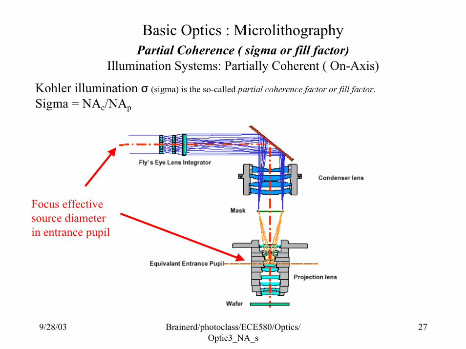
Basic Optics : MicrolithographyPartial Coherence ( sigma or fill factor)
Illumination Systems: Partially Coherent ( On-Axis)
Kohler illumination σ (sigma) is the so-called partial coherence factor or fill factor.
Sigma = NAc/NAp
Focus effective source diameter in entrance pupil
9/28/03 Brainerd/photoclass/ECE580/Optics/Optic3_NA_s
28
Basic Optics : MicrolithographyPartial Coherence ( sigma or fill factor)
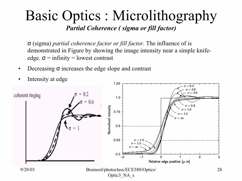
σ (sigma) partial coherence factor or fill factor. The influence of is demonstrated in Figure by showing the image intensity near a simple knife-edge. σ = infinity = lowest contrast
• Decreasing σ increases the edge slope and contrast
• Intensity at edge
9/28/03 Brainerd/photoclass/ECE580/Optics/Optic3_NA_s
29
Basic Optics : MicrolithographyPartial Coherence ( sigma or fill factor)
http://www.mmresearch.com/articles/article4/
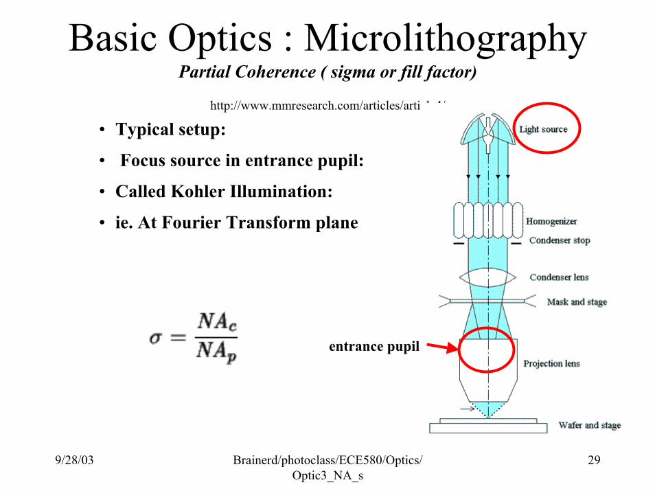
• Typical setup:
• Focus source in entrance pupil:
• Called Kohler Illumination:
• ie. At Fourier Transform plane
entrance pupil
9/28/03 Brainerd/photoclass/ECE580/Optics/Optic3_NA_s
30
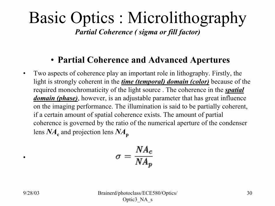
Basic Optics : MicrolithographyPartial Coherence ( sigma or fill factor)
• Partial Coherence and Advanced Apertures • Two aspects of coherence play an important role in lithography. Firstly, the
light is strongly coherent in the time (temporal) domain (color) because of the required monochromaticity of the light source . The coherence in the spatial domain (phase), however, is an adjustable parameter that has great influence on the imaging performance. The illumination is said to be partially coherent, if a certain amount of spatial coherence exists. The amount of partial coherence is governed by the ratio of the numerical aperture of the condenser lens NAc and projection lens NAp
•
9/28/03 Brainerd/photoclass/ECE580/Optics/Optic3_NA_s
31
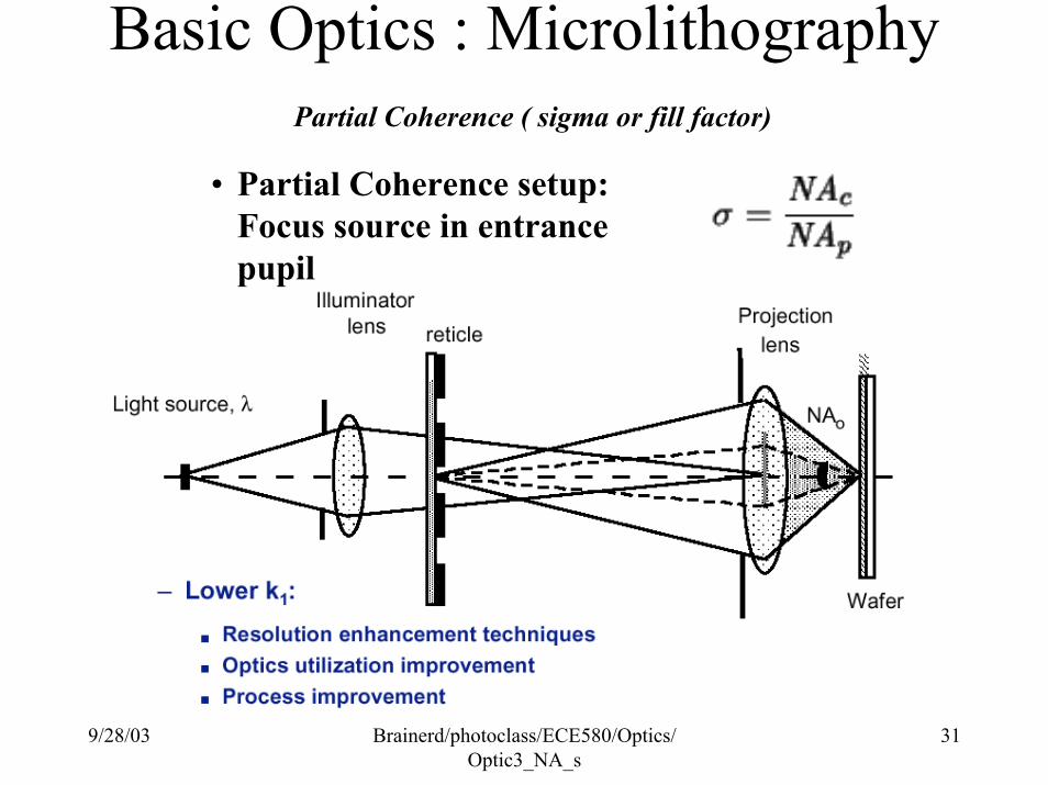
Basic Optics : MicrolithographyPartial Coherence ( sigma or fill factor)
• Partial Coherence setup: Focus source in entrance pupil
•
9/28/03 Brainerd/photoclass/ECE580/Optics/Optic3_NA_s
32
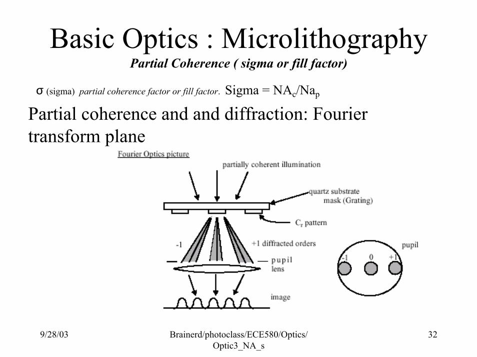
Basic Optics : MicrolithographyPartial Coherence ( sigma or fill factor)
σ (sigma) partial coherence factor or fill factor. Sigma = NAc/Nap
Partial coherence and and diffraction: Fourier transform plane
9/28/03 Brainerd/photoclass/ECE580/Optics/Optic3_NA_s
33
Basic Optics : MicrolithographyMTF and Contrast
9/28/03 Brainerd/photoclass/ECE580/Optics/Optic3_NA_s
34
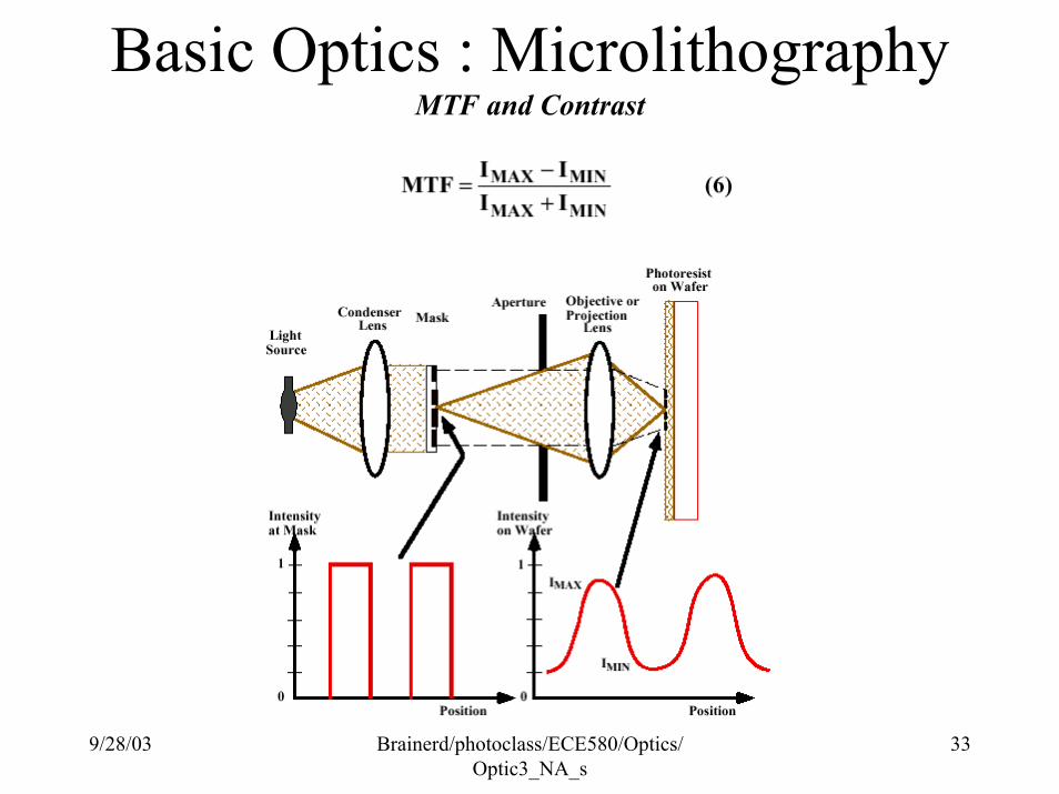
Basic Optics : MicrolithographyMTF and Contrast
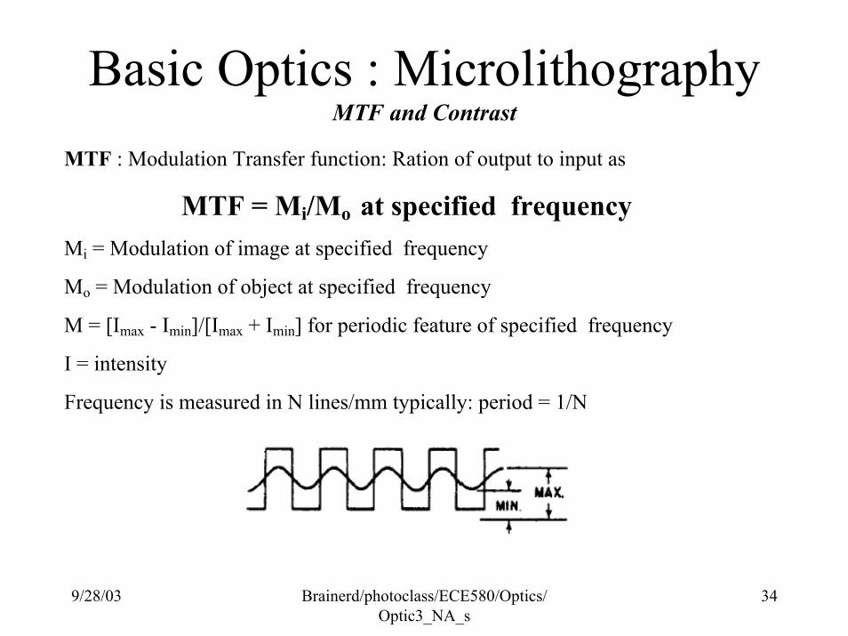
MTF : Modulation Transfer function: Ration of output to input as
MTF = Mi/Mo at specified frequencyMi = Modulation of image at specified frequency
Mo = Modulation of object at specified frequency
M = [Imax - Imin]/[Imax + Imin] for periodic feature of specified frequency
I = intensity
Frequency is measured in N lines/mm typically: period = 1/N
9/28/03 Brainerd/photoclass/ECE580/Optics/Optic3_NA_s
35
Basic Optics : MicrolithographyMTF and Contrast
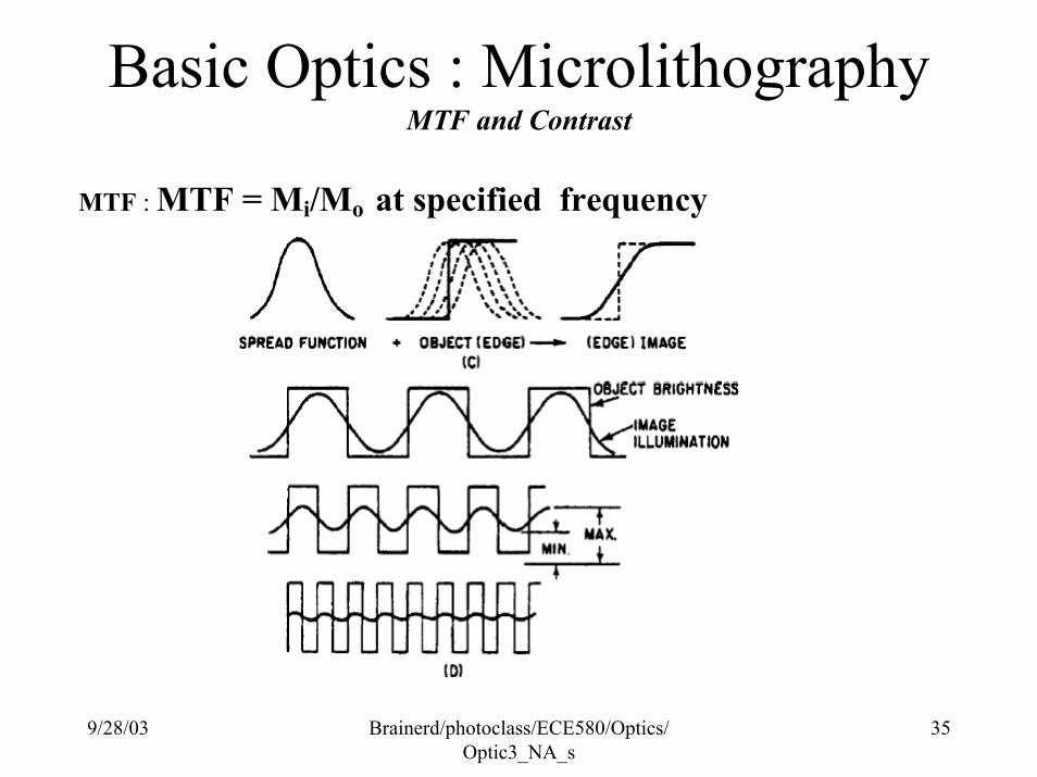
MTF : MTF = Mi/Mo at specified frequency
9/28/03 Brainerd/photoclass/ECE580/Optics/Optic3_NA_s
36
Basic Optics : MicrolithographyMTF and Contrast
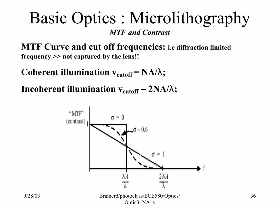
MTF Curve and cut off frequencies: i.e diffraction limited frequency >> not captured by the lens!!
Coherent illumination vcutoff = NA/λ;
Incoherent illumination vcutoff = 2NA/λ;
9/28/03 Brainerd/photoclass/ECE580/Optics/Optic3_NA_s
37
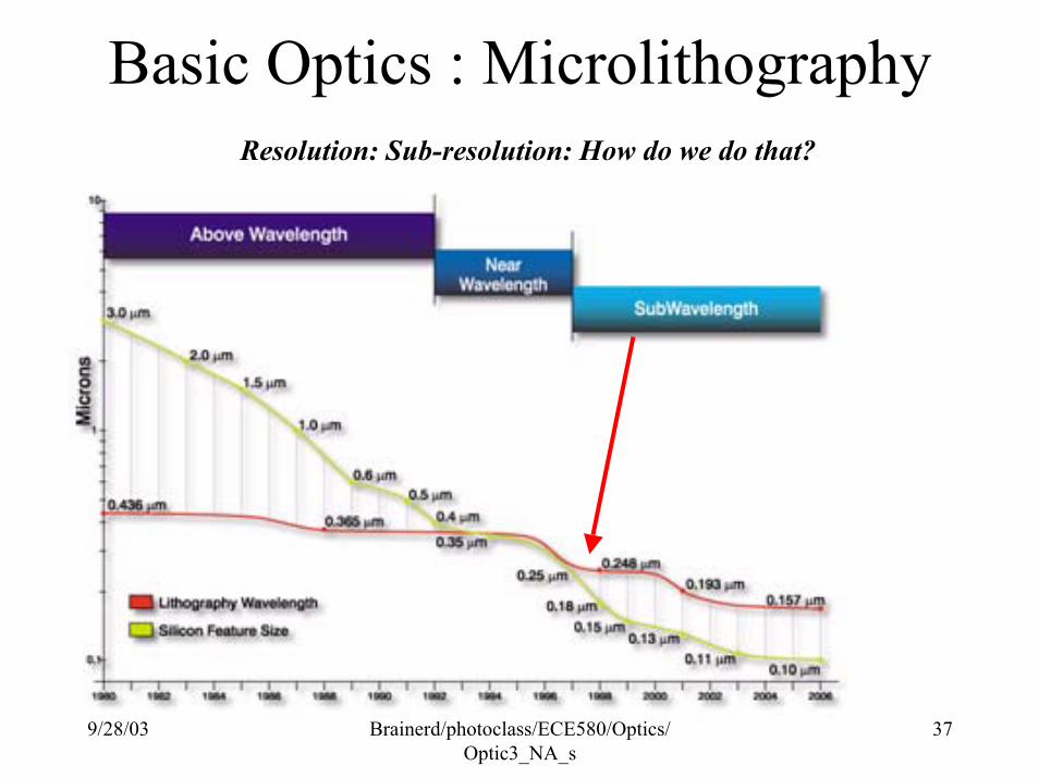
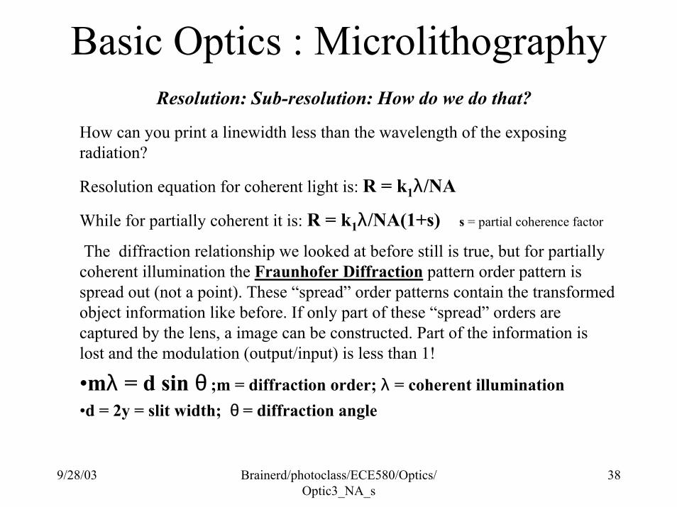
Basic Optics : MicrolithographyResolution: Sub-resolution: How do we do that?
9/28/03 Brainerd/photoclass/ECE580/Optics/Optic3_NA_s
38
Basic Optics : MicrolithographyResolution: Sub-resolution: How do we do that?
How can you print a linewidth less than the wavelength of the exposing radiation?
Resolution equation for coherent light is: R = k1λ/NA
While for partially coherent it is: R = k1λ/NA(1+s) s = partial coherence factor
The diffraction relationship we looked at before still is true, but for partially coherent illumination the Fraunhofer Diffraction pattern order pattern is spread out (not a point). These “spread” order patterns contain the transformed object information like before. If only part of these “spread” orders are captured by the lens, a image can be constructed. Part of the information is lost and the modulation (output/input) is less than 1!
•mλ = d sin θ ;m = diffraction order; λ = coherent illumination•d = 2y = slit width; θ = diffraction angle
9/28/03 Brainerd/photoclass/ECE580/Optics/Optic3_NA_s
39
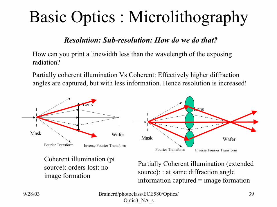
Basic Optics : MicrolithographyResolution: Sub-resolution: How do we do that?
How can you print a linewidth less than the wavelength of the exposing radiation?
Partially coherent illumination Vs Coherent: Effectively higher diffraction angles are captured, but with less information. Hence resolution is increased!
Coherent illumination (pt source): orders lost: no image formation
Partially Coherent illumination (extended source): : at same diffraction angle information captured = image formation
9/28/03 Brainerd/photoclass/ECE580/Optics/Optic3_NA_s
40
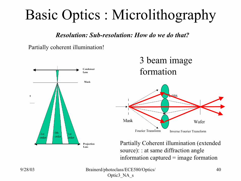
Basic Optics : MicrolithographyResolution: Sub-resolution: How do we do that?
Partially coherent illumination!
3 beam image formation
Partially Coherent illumination (extended source): : at same diffraction angle information captured = image formation
9/28/03 Brainerd/photoclass/ECE580/Optics/Optic3_NA_s
41
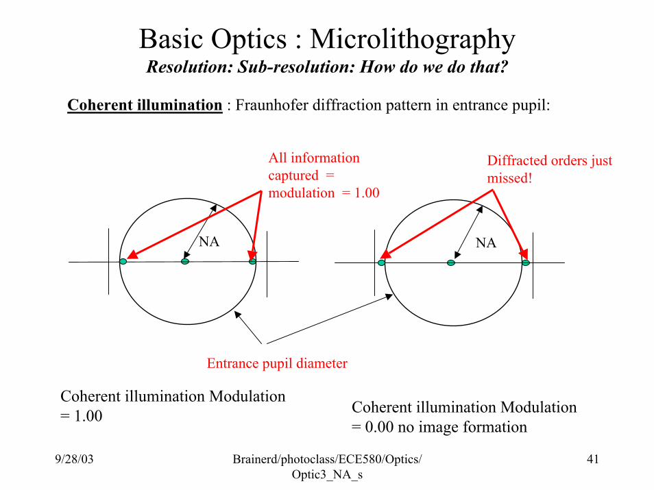
Basic Optics : MicrolithographyResolution: Sub-resolution: How do we do that?
Coherent illumination : Fraunhofer diffraction pattern in entrance pupil:
All information captured = modulation = 1.00
Diffracted orders just missed!
NA NA
Entrance pupil diameter
Coherent illumination Modulation = 1.00 Coherent illumination Modulation
= 0.00 no image formation
9/28/03 Brainerd/photoclass/ECE580/Optics/Optic3_NA_s
42
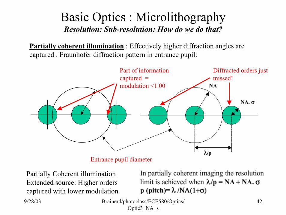
Basic Optics : MicrolithographyResolution: Sub-resolution: How do we do that?
Partially coherent illumination : Effectively higher diffraction angles are captured . Fraunhofer diffraction pattern in entrance pupil:
Part of information captured = modulation <1.00
Entrance pupil diameter
Diffracted orders just missed!
Partially Coherent illumination Extended source: Higher orders captured with lower modulation
9/28/03 Brainerd/photoclass/ECE580/Optics/Optic3_NA_s
43
Basic Optics : MicrolithographyResolution: Sub-resolution: How do we do that?
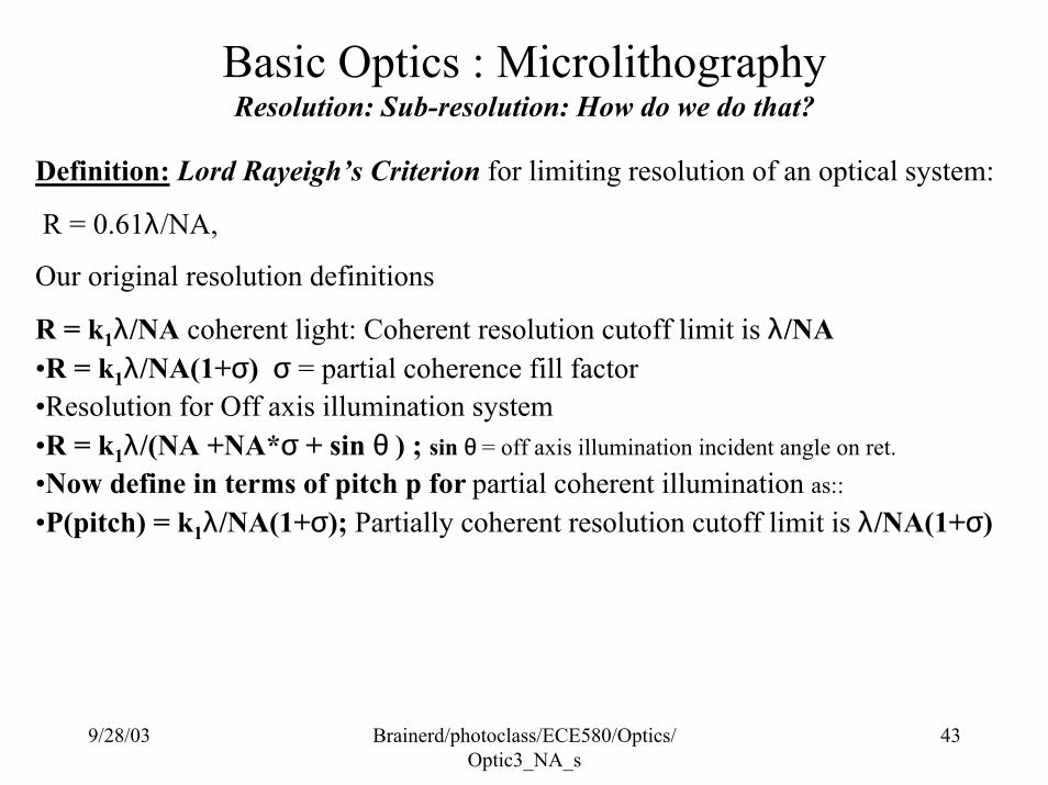
Definition: Lord Rayeigh’s Criterion for limiting resolution of an optical system:
R = 0.61λ/NA,
Our original resolution definitions
R = k1λ/NA coherent light: Coherent resolution cutoff limit is λ/NA•R = k1λ/NA(1+σ) σ = partial coherence fill factor•Resolution for Off axis illumination system•R = k1λ/(NA +NA*σ + sin θ ) ; sin θ = off axis illumination incident angle on ret.•Now define in terms of pitch p for partial coherent illumination as::
•P(pitch) = k1λ/NA(1+σ); Partially coherent resolution cutoff limit is λ/NA(1+σ)
9/28/03 Brainerd/photoclass/ECE580/Optics/Optic3_NA_s
44
Basic Optics : MicrolithographyPartial Coherence ( sigma or fill factor)
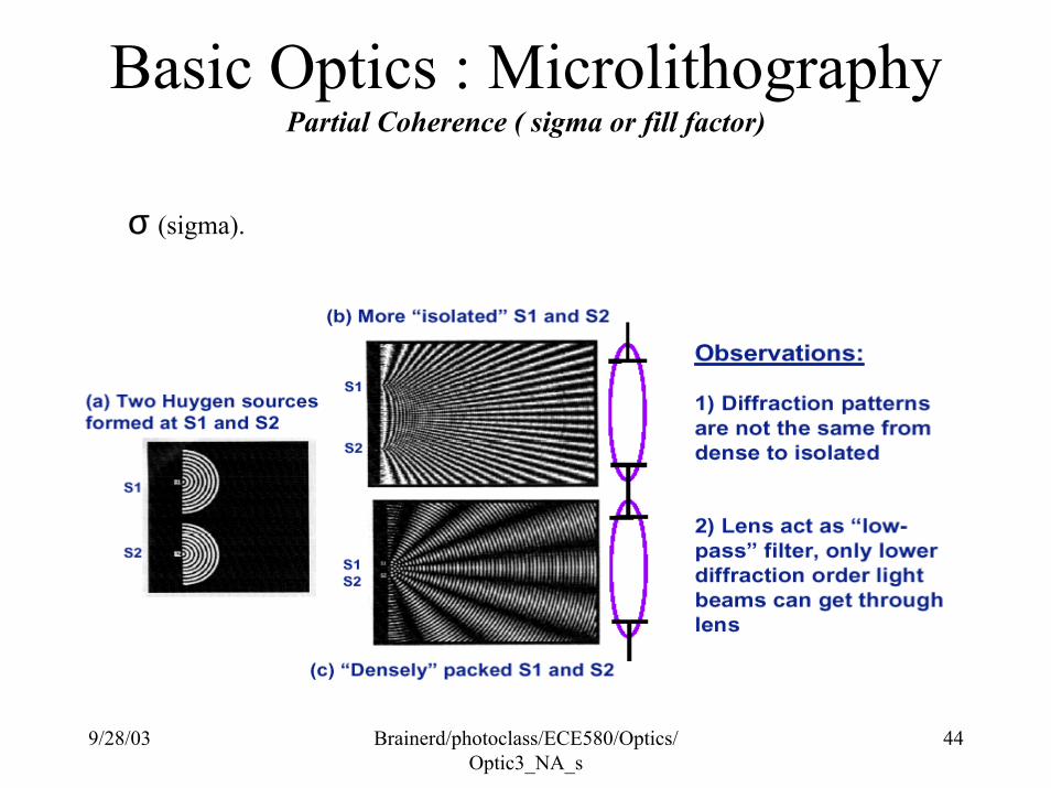
σ (sigma).
9/28/03 Brainerd/photoclass/ECE580/Optics/Optic3_NA_s
45
Basic Optics : MicrolithographyPartial Coherence ( sigma or fill factor)
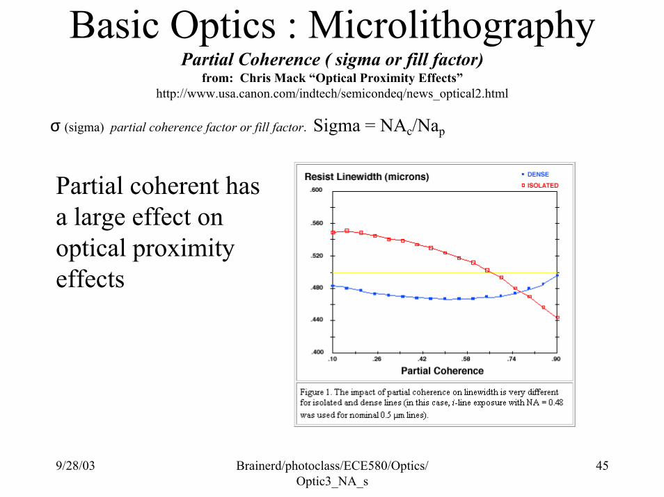
from: Chris Mack “Optical Proximity Effects” http://www.usa.canon.com/indtech/semicondeq/news_optical2.html
σ (sigma) partial coherence factor or fill factor. Sigma = NAc/Nap
Partial coherent has a large effect on optical proximity effects
9/28/03 Brainerd/photoclass/ECE580/Optics/Optic3_NA_s
46
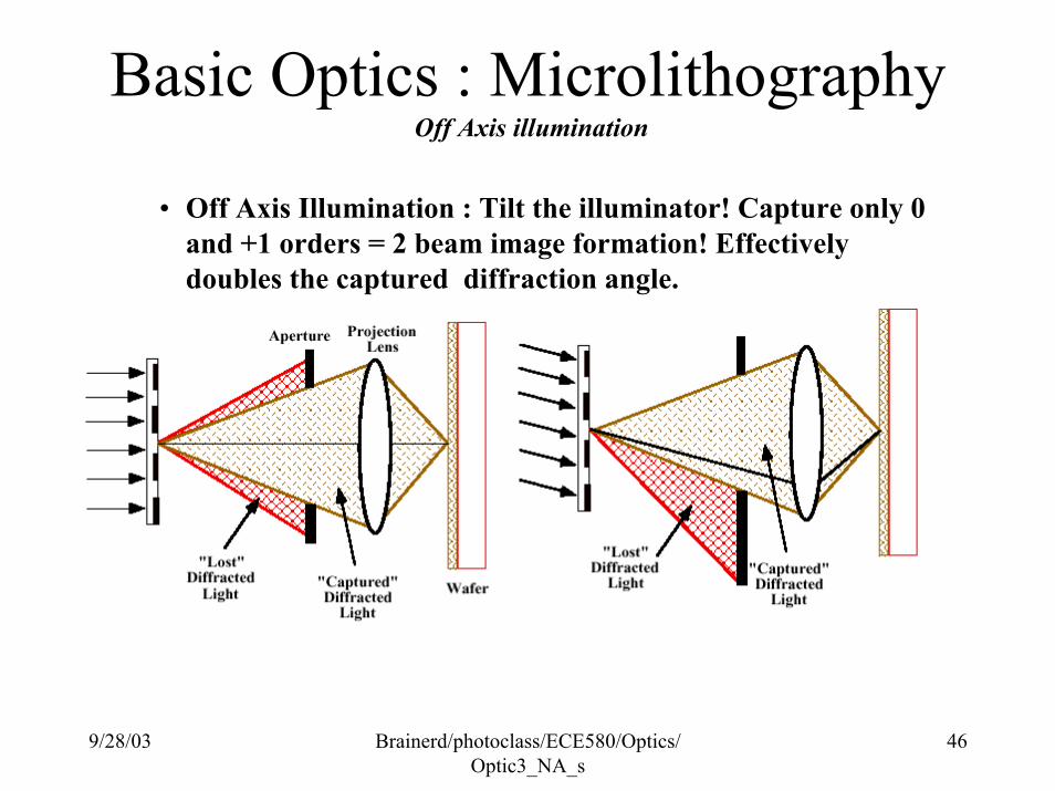
Basic Optics : MicrolithographyOff Axis illumination
• Off Axis Illumination : Tilt the illuminator! Capture only 0 and +1 orders = 2 beam image formation! Effectively doubles the captured diffraction angle.
9/28/03 Brainerd/photoclass/ECE580/Optics/Optic3_NA_s
47
Basic Optics : MicrolithographyOff Axis illumination
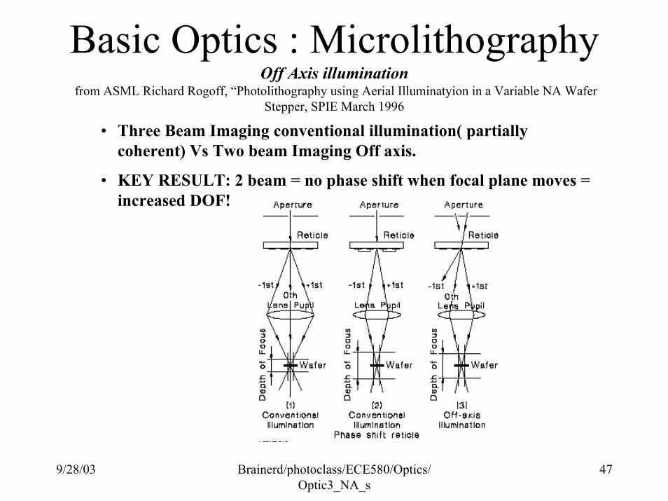
from ASML Richard Rogoff, “Photolithography using Aerial Illuminatyion in a Variable NA Wafer Stepper, SPIE March 1996
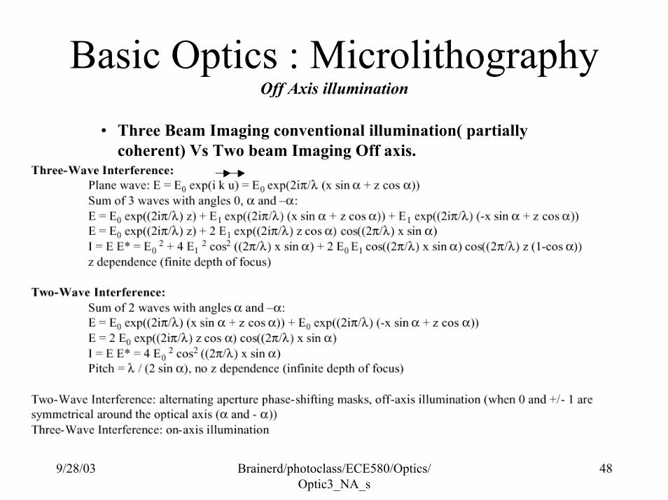
• Three Beam Imaging conventional illumination( partially coherent) Vs Two beam Imaging Off axis.
• KEY RESULT: 2 beam = no phase shift when focal plane moves = increased DOF!
9/28/03 Brainerd/photoclass/ECE580/Optics/Optic3_NA_s
48
Basic Optics : MicrolithographyOff Axis illumination
• Three Beam Imaging conventional illumination( partially coherent) Vs Two beam Imaging Off axis.
9/28/03 Brainerd/photoclass/ECE580/Optics/Optic3_NA_s
49
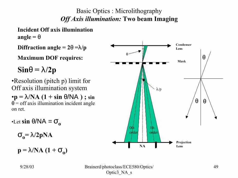
Basic Optics : MicrolithographyOff Axis illumination: Two beam Imaging
Incident Off axis illumination angle = θ
Diffraction angle = 2θ =λ/p
Maximum DOF requires:
Sinθ = λ/2p•Resolution (pitch p) limit for Off axis illumination system•p = λ/NA (1 + sin θ/ΝΑ ) ; sin θ = off axis illumination incident angle on ret.
•Let sin θ/ΝΑ = σo
σo= λ/2pNA
p = λ/NA (1 + σo)
θ
θ θ
9/28/03 Brainerd/photoclass/ECE580/Optics/Optic3_NA_s
50
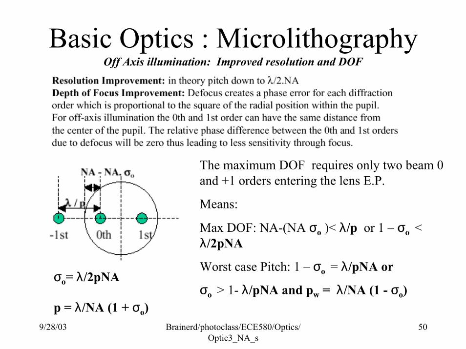
Basic Optics : MicrolithographyOff Axis illumination: Improved resolution and DOF
The maximum DOF requires only two beam 0 and +1 orders entering the lens E.P.
Means:
Max DOF: NA-(NA σo )< λ/p or 1 – σo < λ/2pNA
Worst case Pitch: 1 – σo = λ/pNA or
σo > 1- λ/pNA and pw = λ/NA (1 - σo)σo= λ/2pNA
p = λ/NA (1 + σo)
9/28/03 Brainerd/photoclass/ECE580/Optics/Optic3_NA_s
51
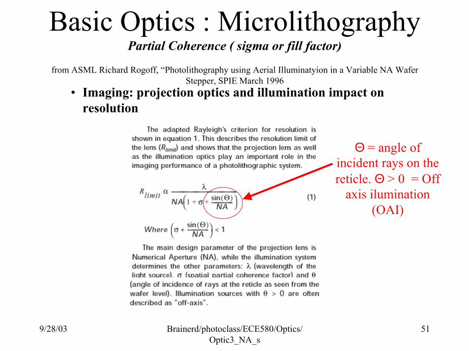
Basic Optics : MicrolithographyPartial Coherence ( sigma or fill factor)
from ASML Richard Rogoff, “Photolithography using Aerial Illuminatyion in a Variable NA Wafer Stepper, SPIE March 1996
• Imaging: projection optics and illumination impact on resolution
Θ = angle of incident rays on thereticle. Θ > 0 = Off
axis ilumination(OAI)
9/28/03 Brainerd/photoclass/ECE580/Optics/Optic3_NA_s
52
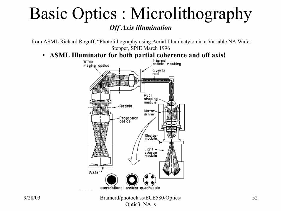
Basic Optics : MicrolithographyOff Axis illumination
from ASML Richard Rogoff, “Photolithography using Aerial Illuminatyion in a Variable NA Wafer Stepper, SPIE March 1996
• ASML Illuminator for both partial coherence and off axis!
9/28/03 Brainerd/photoclass/ECE580/Optics/Optic3_NA_s
53
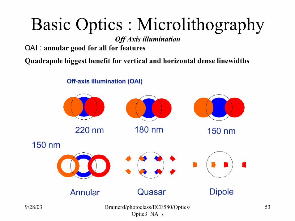
Basic Optics : MicrolithographyOff Axis illumination
ΟΑΙ : annular good for all for features
Quadrapole biggest benefit for vertical and horizontal dense linewidths
9/28/03 Brainerd/photoclass/ECE580/Optics/Optic3_NA_s
54
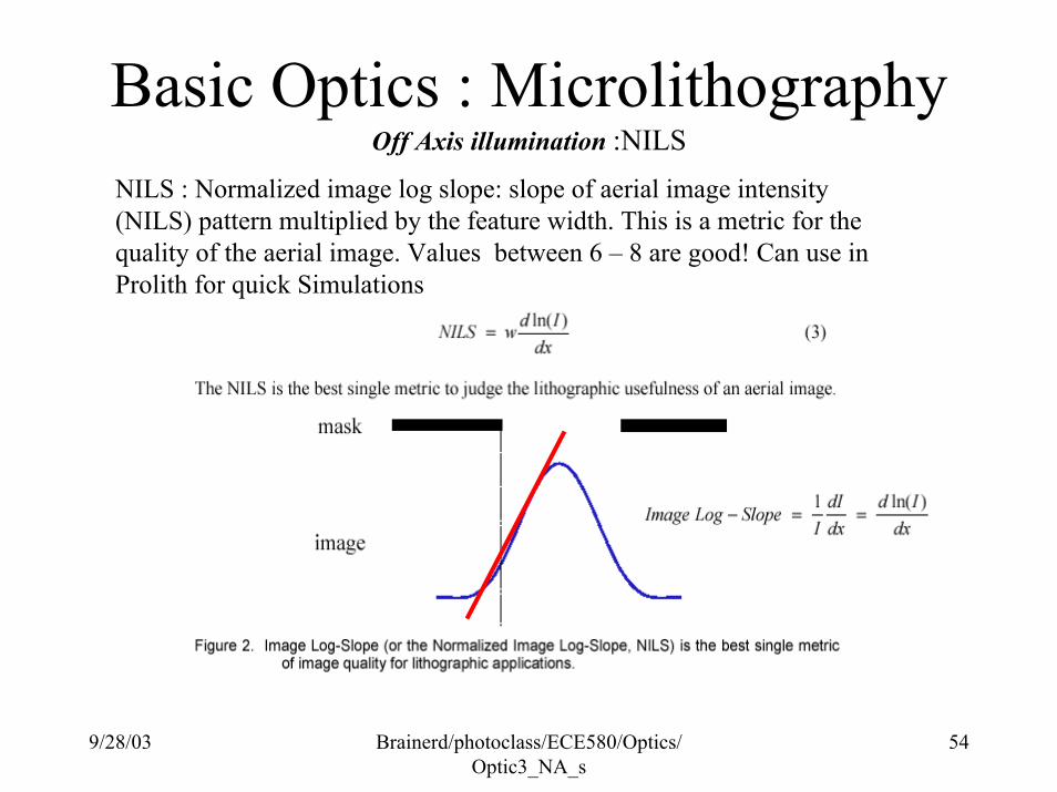
Basic Optics : MicrolithographyOff Axis illumination :NILS
NILS : Normalized image log slope: slope of aerial image intensity (NILS) pattern multiplied by the feature width. This is a metric for the quality of the aerial image. Values between 6 – 8 are good! Can use inProlith for quick Simulations
9/28/03 Brainerd/photoclass/ECE580/Optics/Optic3_NA_s
55
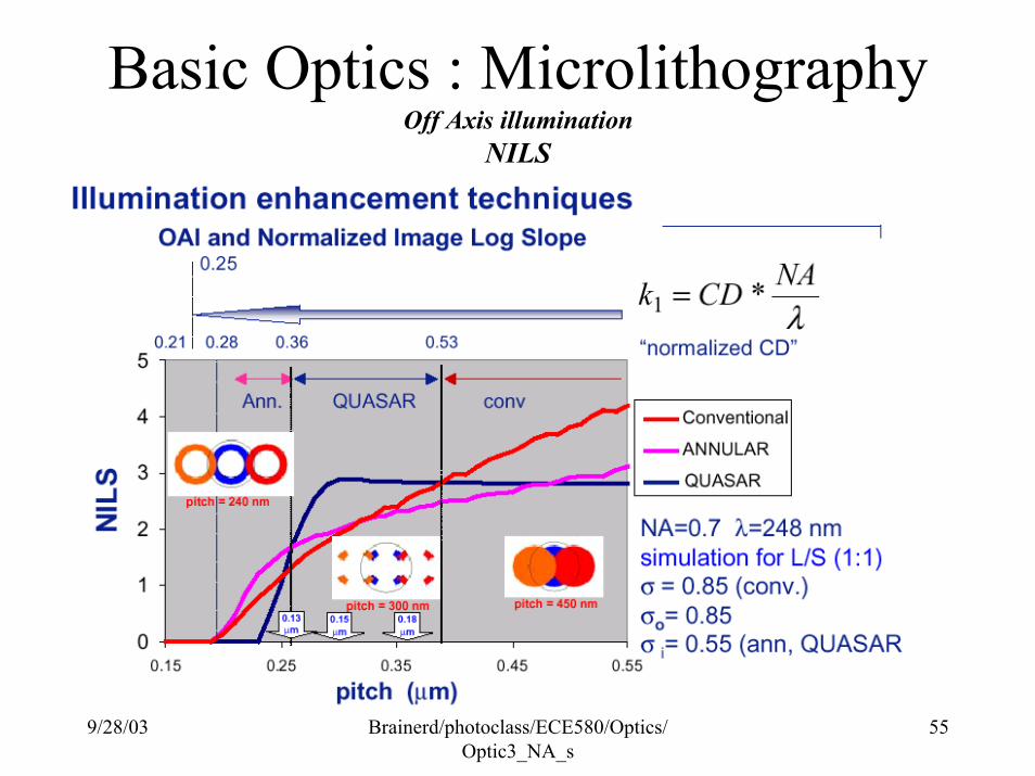
Basic Optics : MicrolithographyOff Axis illumination
NILS
9/28/03 Brainerd/photoclass/ECE580/Optics/Optic3_NA_s
56
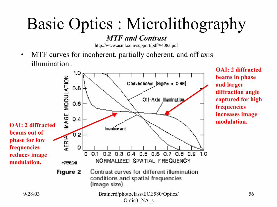
Basic Optics : MicrolithographyMTF and Contrast
http://www.asml.com/support/pdf/94083.pdf
• MTF curves for incoherent, partially coherent, and off axis illumination..
OAI: 2 diffracted beams out of phase for low frequencies reduces image modulation.
OAI: 2 diffracted beams in phase and larger diffraction angle captured for high frequencies increases image modulation.
9/28/03 Brainerd/photoclass/ECE580/Optics/Optic3_NA_s
57
Basic Optics : MicrolithographyResolution, Depth of Focus, and Depth of field
• Forbidden Pitch• Understanding the Forbidden Pitch Phenomenon and Assist Feature Placement
• Xuelong Shi1, Stephen Hsu1, Fung Chen1, Michael Hsu1, Robert J. Socha2, Micea Dusa2
1. ASML MaskTools, Inc. 4800 Great America Parkway, Suite 400, Santa Clara, CA 950542. ASML, TDC Group 4800 Great America Parkway, Suite 400, Santa Clara, CA 95054
Presented at SPIE, 2002 • Abstract
• Optical proximity effect is a well-known phenomenon in photolithography. Such an effect results from the structural interaction between the main feature and the neighboring features. Recent observations have shown that such structural interactions not only affect the critical dimension of the main feature at the image plane, but also the exposure latitude of the main feature. In this paper, it has been shown that the variation of the critical dimension as well as the exposure latitude of the main feature is a direct consequence of light field interference between the main feature and the neighboring features. Depending on the phase of the field produced by the neighboring features, the main feature exposure latitude can be improved by constructive light field interference, or degraded by destructive light field interference.
• The phase of the field produced by the neighboring features can be shown to be dependent on the pitch as well as the illumination angle. For a given illumination, the forbidden pitch lies in the location where the field produced by the neighboring features interferes with the field of the main feature destructively. The theoretical analysis given here offers the tool to map out the forbidden pitch locations for any feature size and illumination conditions. More importantly, it provides the theoretical ground for illumination design in order to suppress the forbidden pitch phenomenon, and for scattering bar placement to achieve optimal performance as well.
9/28/03 Brainerd/photoclass/ECE580/Optics/Optic3_NA_s
58
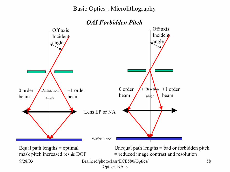
Basic Optics : Microlithography
OAI Forbidden Pitch
Wafer Plane
Lens EP or NA
Off axis Incident angle
0 order beam
Diffraction
angle
Unequal path lengths = bad or forbidden pitch = reduced image contrast and resolution
Off axis Incident angle
0 order beam
Diffraction
angle
+1 order beam
Equal path lengths = optimal mask pitch increased res & DOF
+1 order beam
9/28/03 Brainerd/photoclass/ECE580/Optics/Optic3_NA_s
59
Basic Optics : Microlithography
OAI Forbidden PitchOff axis Incident angle
0 order beam
Diffraction
angle
Unequal path lengths = bad or forbidden pitch = reduced image contrast and resolution
Wafer Plane
Lens EP or NA
+1 order beam
Unequal path lengths result in poor image contrast
9/28/03 Brainerd/photoclass/ECE580/Optics/Optic3_NA_s
60
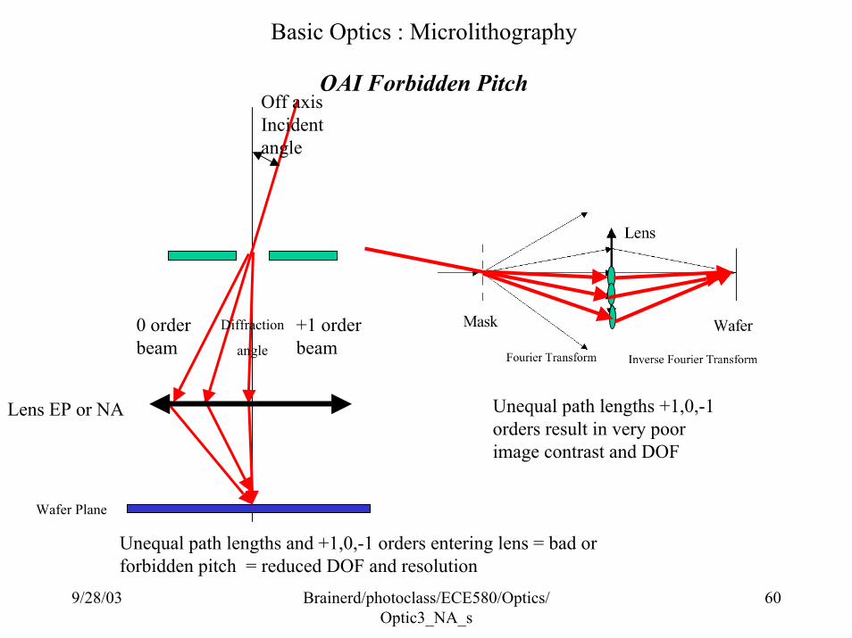
Basic Optics : Microlithography
OAI Forbidden PitchOff axis Incident angle
0 order beam
Diffraction
angle
Wafer Plane
Lens EP or NA
+1 order beam
Unequal path lengths +1,0,-1 orders result in very poor image contrast and DOF
Unequal path lengths and +1,0,-1 orders entering lens = bad or forbidden pitch = reduced DOF and resolution
9/28/03 Brainerd/photoclass/ECE580/Optics/Optic3_NA_s
61
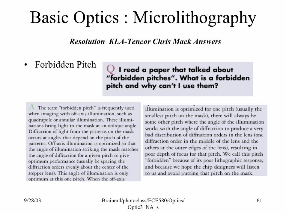
Basic Optics : MicrolithographyResolution KLA-Tencor Chris Mack Answers
• Forbidden Pitch
9/28/03 Brainerd/photoclass/ECE580/Optics/Optic3_NA_s
62
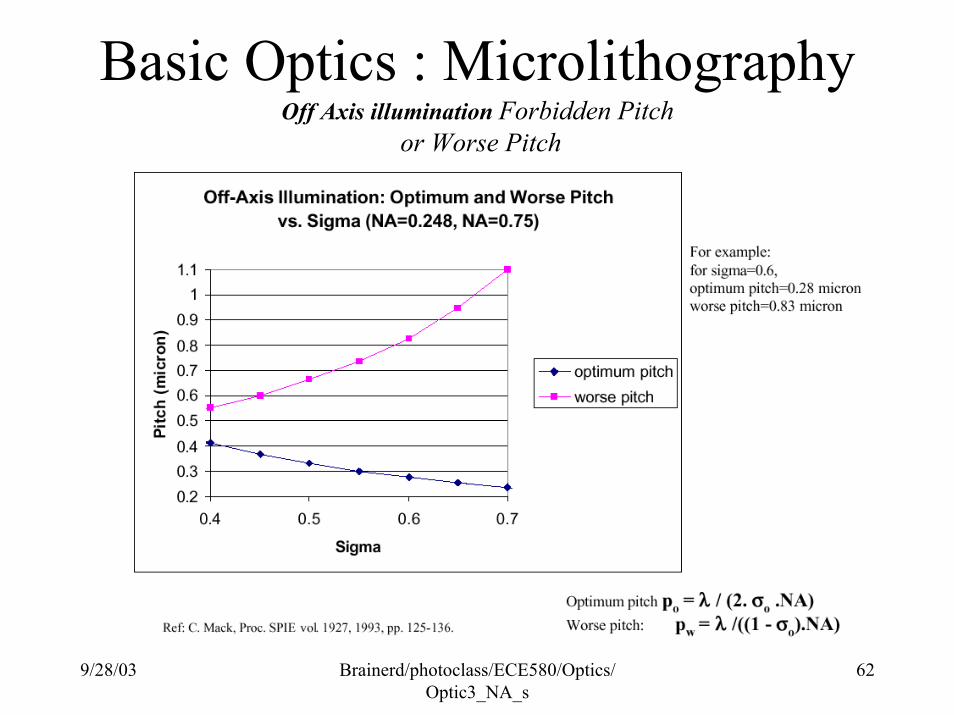
Basic Optics : MicrolithographyOff Axis illumination Forbidden Pitch
or Worse Pitch
9/28/03 Brainerd/photoclass/ECE580/Optics/Optic3_NA_s
63
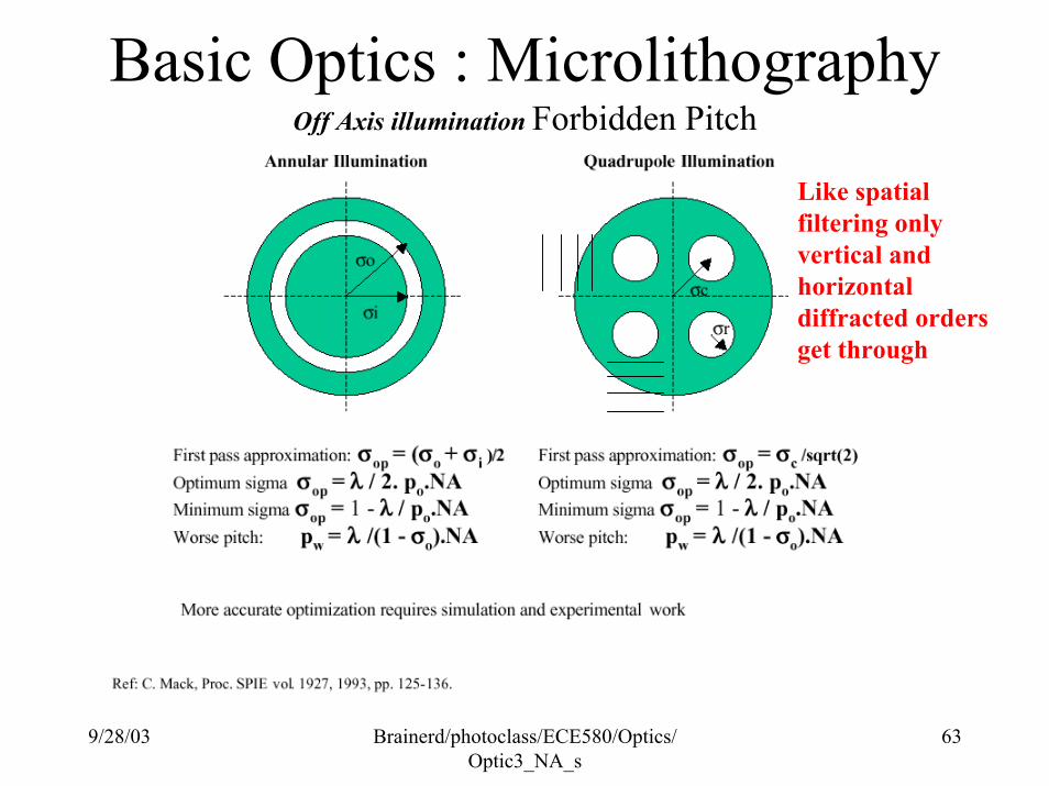
Basic Optics : MicrolithographyOff Axis illumination Forbidden Pitch
Like spatial filtering only vertical and horizontal diffracted orders get through
9/28/03 Brainerd/photoclass/ECE580/Optics/Optic3_NA_s
64
Basic Optics : MicrolithographyProjection printing: Telecentric system
• Telecentricity: Source is focused in entrance pupil:• Image side: Image size (magnification) is
invariant with wafer defocus!• Object side: Image size (magnification) is
invariant with object position.
9/28/03 Brainerd/photoclass/ECE580/Optics/Optic3_NA_s
65
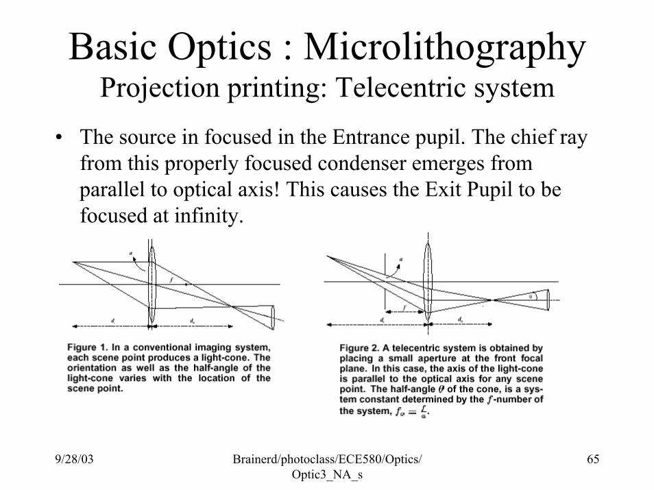
Basic Optics : MicrolithographyProjection printing: Telecentric system
• The source in focused in the Entrance pupil. The chief ray from this properly focused condenser emerges from parallel to optical axis! This causes the Exit Pupil to be focused at infinity.
9/28/03 Brainerd/photoclass/ECE580/Optics/Optic3_NA_s
66
Basic Optics : MicrolithographyProjection printing: Telecentric system
• The condenser lens is used to focus the source in the entrance pupil.
• PROPER CONDENSER FOCUS: Source focused in Entrance pupil: chief ray emerges from parallel to optical axis! This causes the Exit Pupil to be focused at infinity. Image location ( I.e. defocused) does not change image size (magnification).
• POSITIVE CONDENSER FOCUS: Source focused before entrance pupil: chief ray emerges converging! Image location ( I.e. defocused) causes change in image size (magnification). Image is smaller as the image plane moves away from the optical best focus.
• NEGATIVE CONDENSER FOCUS: Source focused behind entrance pupil: chief ray emerges diverging! Image location ( I.e. defocused) causes change in image size (magnification). Image islarger as the image plane moves away from the optical best focus.
9/28/03 Brainerd/photoclass/ECE580/Optics/Optic3_NA_s
67
Basic Optics : MicrolithographyProjection printing: Telecentric system
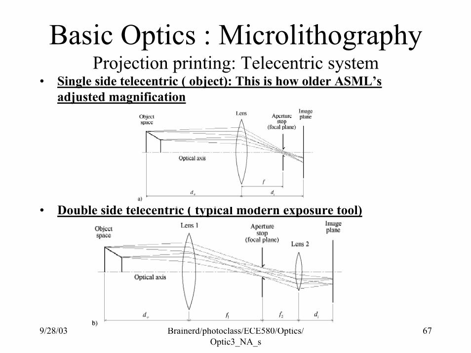
• Single side telecentric ( object): This is how older ASML’sadjusted magnification
• Double side telecentric ( typical modern exposure tool)
9/28/03 Brainerd/photoclass/ECE580/Optics/Optic3_NA_s
68
Basic Optics : MicrolithographyProjection printing: Telecentric system
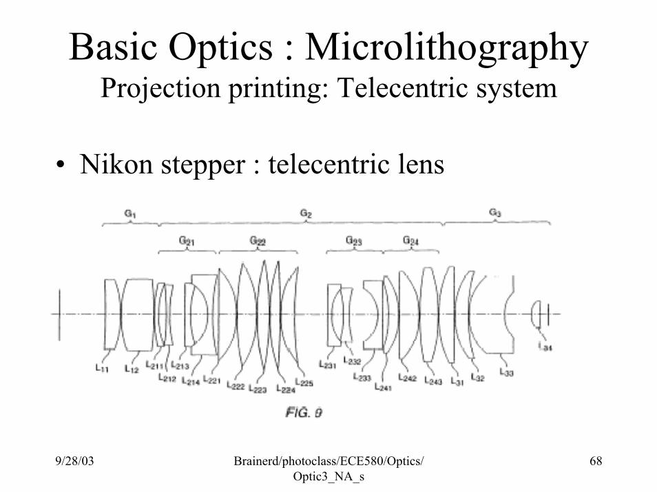
• Nikon stepper : telecentric lens
9/28/03 Brainerd/photoclass/ECE580/Optics/Optic3_NA_s
69
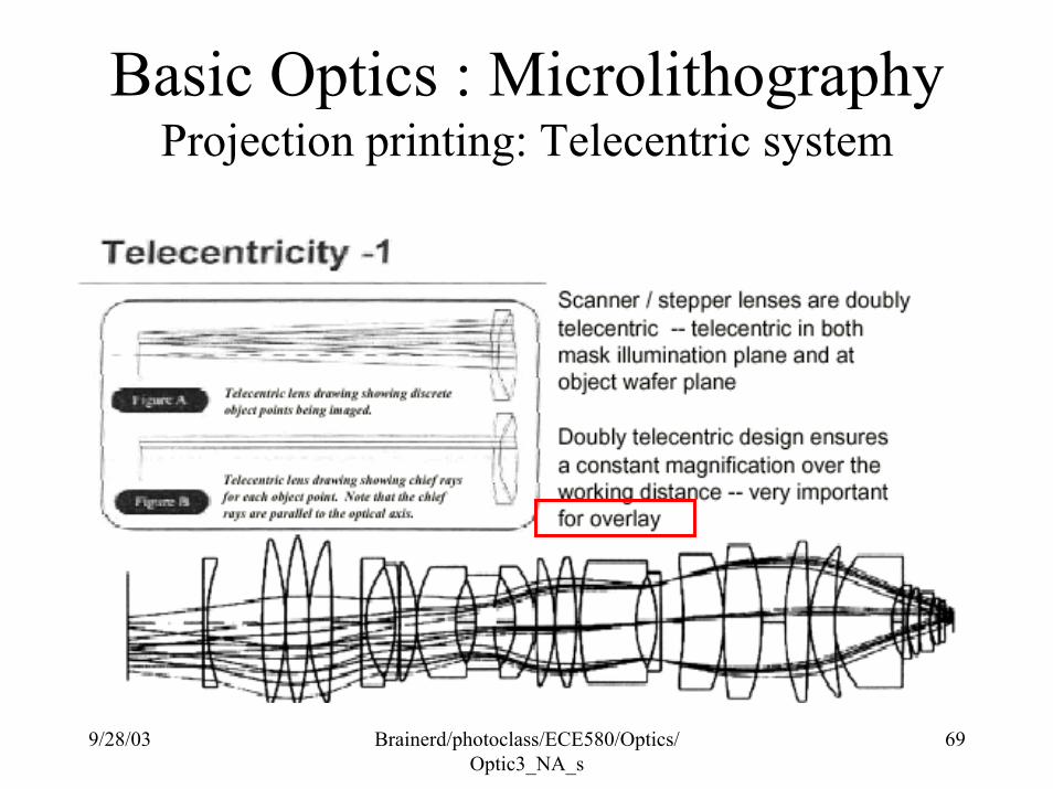
Basic Optics : MicrolithographyProjection printing: Telecentric system
9/28/03 Brainerd/photoclass/ECE580/Optics/Optic3_NA_s
70
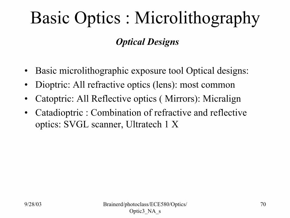
Basic Optics : MicrolithographyOptical Designs
• Basic microlithographic exposure tool Optical designs:• Dioptric: All refractive optics (lens): most common• Catoptric: All Reflective optics ( Mirrors): Micralign• Catadioptric : Combination of refractive and reflective
optics: SVGL scanner, Ultratech 1 X
9/28/03 Brainerd/photoclass/ECE580/Optics/Optic3_NA_s
71
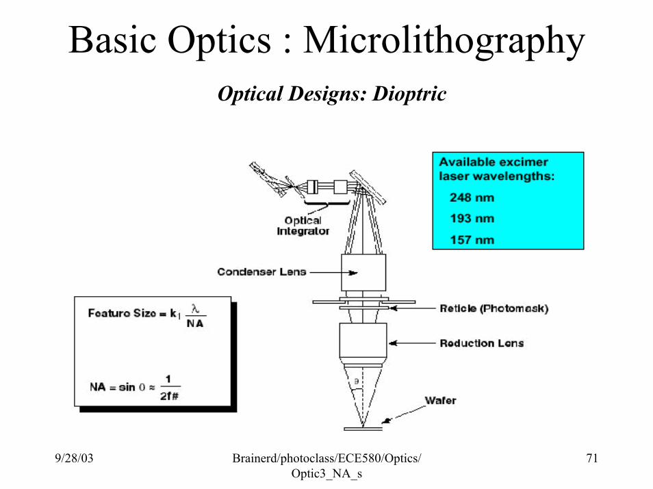
Basic Optics : MicrolithographyOptical Designs: Dioptric
9/28/03 Brainerd/photoclass/ECE580/Optics/Optic3_NA_s
72
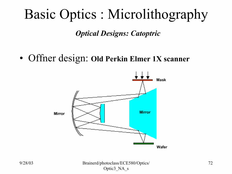
Basic Optics : MicrolithographyOptical Designs: Catoptric
• Offner design: Old Perkin Elmer 1X scanner
9/28/03 Brainerd/photoclass/ECE580/Optics/Optic3_NA_s
73
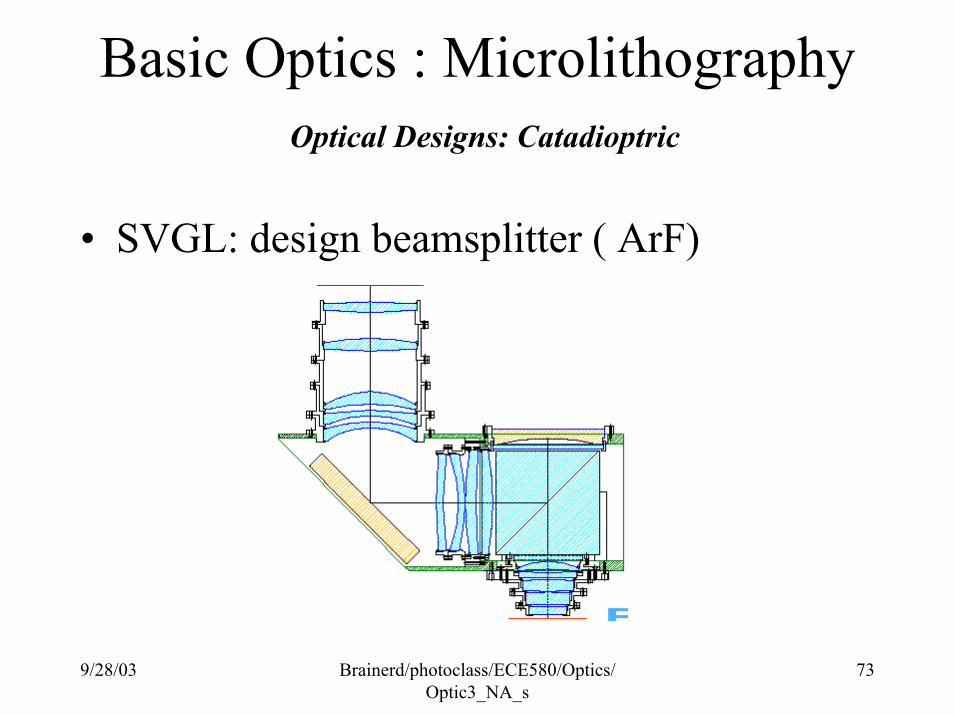
Basic Optics : MicrolithographyOptical Designs: Catadioptric
• SVGL: design beamsplitter ( ArF)
9/28/03 Brainerd/photoclass/ECE580/Optics/Optic3_NA_s
74
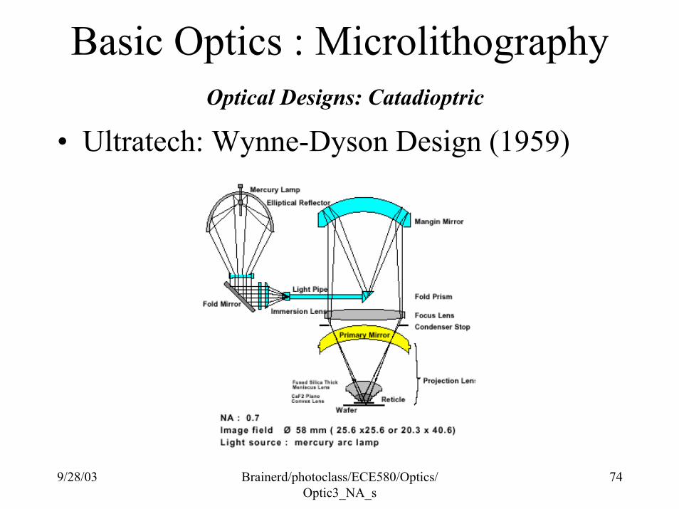
Basic Optics : MicrolithographyOptical Designs: Catadioptric
• Ultratech: Wynne-Dyson Design (1959)