Embed Size (px)
Citation preview

International Journal of Sustainable and Green Energy 2015; 4(5): 187-194
Published online September 11, 2015 (http://www.sciencepublishinggroup.com/j/ijsge)
doi: 10.11648/j.ijrse.20150405.13
Basic Guidelines for LED Lamp Package Design
Song Jae Lee
Electronics Engineering Department, Chungnam National University, Daejeon, Korea
Email address: [email protected]
To cite this article: Song Jae Lee. Basic Guidelines for LED Lamp Package Design. Basic Guidelines for LED Lamp Package Design.
Vol. 4, No. 5, 2015, pp. 187-194. doi: 10.11648/j.ijrse.20150405.13
Abstract: Even though significant amount of researches has been done to develop LED lamp packages for improved
performance especially in terms of output power, it is believed that no standard theories or guidelines have been established yet
for designing LED lamp packages. In this paper, both the InGaN/Sapphire LED chip structure and its Epi-Up or Epi-Down
chip-mounting scheme have been analyzed by using Monte Carlo photon simulation method. Based on the analysis, we have
established guidelines for designing LED lamp packages.
Keywords: LED, LED Lamp, LED Lamp Package Design
1. Introduction
Even though visible light-emitting diodes (LEDs) have
been commercially very successful, it is believed that the
basic principles or guidelines for designing LED lamp
packages may not have been well established yet.
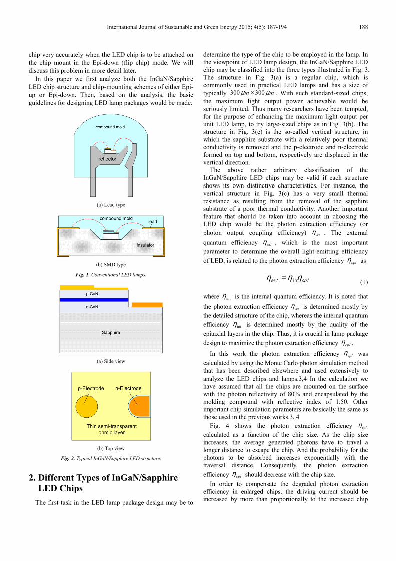
Conventional LED lamps in general may fall into either
the leaded type or SMD (surface mount design) type as
schematically described in Fig. 1. The leaded type has
relatively long leads that are often to be inserted through the
holes made in the printed circuit board (PCB) and soldered at
the bottom. On the other hand, the SMD type has structures
that are more suited to be attached directly on the top surface
of the PCB. Even though the leaded type LED lamps are still
used extensively, for instance, in applications such as traffic
lights and outdoor displays, the general trend seems to favor
ever more the SMD type LED lamps.
A serious problem in the SMD structure shown in Fig. 1(b)
may be that the heat generated in the LED chip is not
dissipated easily. In general, both the molding compounds
encapsulating both the LED chip and the dielectric chip
mount have relatively poor thermal conductivities. Thus, in
order to prevent severe heating in the junction of the chip, the
LED driving current should be kept relatively small leading
to very limited light output. In general, the more the junction
temperature rises, the more likely the injected electrons and
holes recombine nonradiatively or overflow to the carrier
confinement layers and lead to significantly decreased
internal quantum efficiency.1 In addition, the rise of the
junction temperature would in general shrink the bandgap
energy of the active layer, which in turn shifts the spectrum
to the red and changes the color of the light output.
The key component of the LED lamp is obviously the LED
chip. Thus it would be a first task in LED lamp design to
accurately analyze LED chips. Fig. 2 shows a typical
structure of the InGaN/Sapphire LED chip, which currently
enjoys a commanding position in visible LEDs. They have
excellent reliability and brightness. Furthermore their
emission spectrum from ultraviolet to amber is much broader
than that of the AlInGaP/GaAs system that emits mostly in
the red spectral region.2 It is noted also that the blue emission
from InGaN/Sapphire LEDs is exploited to implement the
white LEDs that are essential for the general lighting. As well
known, blue LEDs can also be fabricated by using the
InGaN/SiC system. However, they may hardly compete with
the InGaN/Sapphire LEDs especially in terms of maximum
light output and reliability.
InGaN/Sapphire LEDs are grown on the non-conducting
sapphire substrate and, as a result, their chip structures are
quite unique in that the two electrodes both formed on the
epitaxial side are displaced from each other in the lateral
direction. Another important feature of the electrode design is
that a very thin semi-transparent p-ohmic material is
deposited on the top surface of the p-GaN carrier
confinement layer outside the p-electrode pad. The thin
ohmic material is to compensate the very low conductivity of
the p-GaN carrier confinement layer and prevents the driving
voltage from rising too much. The deposition of the thin
ohmic material outside the p-electrode would make the
isolation distance between two electrodes as small as
typically 10~20 mµ . It is noted that this small separation
between the two electrodes would make it crucial to align the
International Journal of Sustainable and Green Energy 2015; 4(5): 187-194 188
chip very accurately when the LED chip is to be attached on
the chip mount in the Epi-down (flip chip) mode. We will
discuss this problem in more detail later.
In this paper we first analyze both the InGaN/Sapphire
LED chip structure and chip-mounting schemes of either Epi-
up or Epi-down. Then, based on the analysis, the basic
guidelines for designing LED lamp packages would be made.
(a) Lead type
(b) SMD type
Fig. 1. Conventional LED lamps.
(a) Side view
(b) Top view
Fig. 2. Typical InGaN/Sapphire LED structure.
2. Different Types of InGaN/Sapphire
LED Chips
The first task in the LED lamp package design may be to
determine the type of the chip to be employed in the lamp. In
the viewpoint of LED lamp design, the InGaN/Sapphire LED
chip may be classified into the three types illustrated in Fig. 3.
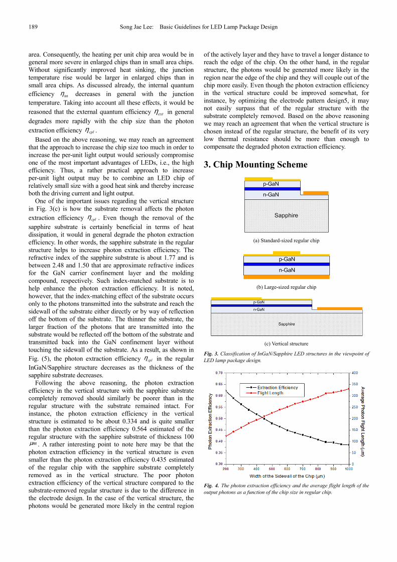
The structure in Fig. 3(a) is a regular chip, which is
commonly used in practical LED lamps and has a size of
typically mm µµ 300300 × . With such standard-sized chips,
the maximum light output power achievable would be
seriously limited. Thus many researchers have been tempted,
for the purpose of enhancing the maximum light output per
unit LED lamp, to try large-sized chips as in Fig. 3(b). The
structure in Fig. 3(c) is the so-called vertical structure, in
which the sapphire substrate with a relatively poor thermal
conductivity is removed and the p-electrode and n-electrode
formed on top and bottom, respectively are displaced in the
vertical direction.
The above rather arbitrary classification of the
InGaN/Sapphire LED chips may be valid if each structure
shows its own distinctive characteristics. For instance, the
vertical structure in Fig. 3(c) has a very small thermal
resistance as resulting from the removal of the sapphire
substrate of a poor thermal conductivity. Another important
feature that should be taken into account in choosing the
LED chip would be the photon extraction efficiency (or
photon output coupling efficiency) cplη . The external
quantum efficiency extη , which is the most important
parameter to determine the overall light-emitting efficiency
of LED, is related to the photon extraction efficiency cplη as
cplext ηηη int= (1)
where intη is the internal quantum efficiency. It is noted that
the photon extraction efficiency cplη is determined mostly by
the detailed structure of the chip, whereas the internal quantum
efficiency intη is determined mostly by the quality of the
epitaxial layers in the chip. Thus, it is crucial in lamp package
design to maximize the photon extraction efficiency cplη .
In this work the photon extraction efficiency cplη was
calculated by using the Monte Carlo photon simulation method
that has been described elsewhere and used extensively to
analyze the LED chips and lamps.3,4 In the calculation we
have assumed that all the chips are mounted on the surface
with the photon reflectivity of 80% and encapsulated by the
molding compound with reflective index of 1.50. Other
important chip simulation parameters are basically the same as
those used in the previous works.3, 4
Fig. 4 shows the photon extraction efficiency cplη
calculated as a function of the chip size. As the chip size
increases, the average generated photons have to travel a
longer distance to escape the chip. And the probability for the
photons to be absorbed increases exponentially with the
traversal distance. Consequently, the photon extraction
efficiency cplη should decrease with the chip size.
In order to compensate the degraded photon extraction
efficiency in enlarged chips, the driving current should be
increased by more than proportionally to the increased chip
189 Song Jae Lee: Basic Guidelines for LED Lamp Package Design
area. Consequently, the heating per unit chip area would be in
general more severe in enlarged chips than in small area chips.
Without significantly improved heat sinking, the junction
temperature rise would be larger in enlarged chips than in
small area chips. As discussed already, the internal quantum
efficiency intη decreases in general with the junction
temperature. Taking into account all these effects, it would be
reasoned that the external quantum efficiency extη in general
degrades more rapidly with the chip size than the photon
extraction efficiency cplη .
Based on the above reasoning, we may reach an agreement
that the approach to increase the chip size too much in order to
increase the per-unit light output would seriously compromise
one of the most important advantages of LEDs, i.e., the high
efficiency. Thus, a rather practical approach to increase
per-unit light output may be to combine an LED chip of
relatively small size with a good heat sink and thereby increase
both the driving current and light output.
One of the important issues regarding the vertical structure
in Fig. 3(c) is how the substrate removal affects the photon
extraction efficiency cplη . Even though the removal of the
sapphire substrate is certainly beneficial in terms of heat
dissipation, it would in general degrade the photon extraction
efficiency. In other words, the sapphire substrate in the regular
structure helps to increase photon extraction efficiency. The
refractive index of the sapphire substrate is about 1.77 and is
between 2.48 and 1.50 that are approximate refractive indices
for the GaN carrier confinement layer and the molding
compound, respectively. Such index-matched substrate is to
help enhance the photon extraction efficiency. It is noted,
however, that the index-matching effect of the substrate occurs
only to the photons transmitted into the substrate and reach the
sidewall of the substrate either directly or by way of reflection
off the bottom of the substrate. The thinner the substrate, the
larger fraction of the photons that are transmitted into the
substrate would be reflected off the bottom of the substrate and
transmitted back into the GaN confinement layer without
touching the sidewall of the substrate. As a result, as shown in
Fig. (5), the photon extraction efficiency cplη in the regular
InGaN/Sapphire structure decreases as the thickness of the
sapphire substrate decreases.
Following the above reasoning, the photon extraction
efficiency in the vertical structure with the sapphire substrate
completely removed should similarly be poorer than in the
regular structure with the substrate remained intact. For
instance, the photon extraction efficiency in the vertical
structure is estimated to be about 0.334 and is quite smaller
than the photon extraction efficiency 0.564 estimated of the
regular structure with the sapphire substrate of thickness 100 mµ . A rather interesting point to note here may be that the
photon extraction efficiency in the vertical structure is even
smaller than the photon extraction efficiency 0.435 estimated
of the regular chip with the sapphire substrate completely
removed as in the vertical structure. The poor photon
extraction efficiency of the vertical structure compared to the
substrate-removed regular structure is due to the difference in
the electrode design. In the case of the vertical structure, the
photons would be generated more likely in the central region
of the actively layer and they have to travel a longer distance to
reach the edge of the chip. On the other hand, in the regular
structure, the photons would be generated more likely in the
region near the edge of the chip and they will couple out of the
chip more easily. Even though the photon extraction efficiency
in the vertical structure could be improved somewhat, for
instance, by optimizing the electrode pattern design5, it may
not easily surpass that of the regular structure with the
substrate completely removed. Based on the above reasoning
we may reach an agreement that when the vertical structure is
chosen instead of the regular structure, the benefit of its very
low thermal resistance should be more than enough to
compensate the degraded photon extraction efficiency.
3. Chip Mounting Scheme
(a) Standard-sized regular chip
(b) Large-sized regular chip
(c) Vertical structure
Fig. 3. Classification of InGaN/Sapphire LED structures in the viewpoint of
LED lamp package design.
Fig. 4. The photon extraction efficiency and the average flight length of the
output photons as a function of the chip size in regular chip.

International Journal of Sustainable and Green Energy 2015; 4(5): 187-194 190
Fig. 5. Photon extraction efficiency as a function of the sapphire substrate
thickness in regular chip.
(a) Epi-Up on metallic chip mount
(b) Epi-Down on dielectric chip mount
(c) Epi-Down on metallic chip mount
(d) Epi-Down on Si-submount
Fig. 6. Chip mounting schemes.
Fig. 7. Photon extraction efficiency as a function of the chip size, depending
on chip-mounting schemes.
Once the type of the LED chip is chosen to be employed in
the lamp packaging, the next important task may be to decide
how to attach the chip on the chip mount. In general the
performance of the chip, in terms of both the heat dissipation
and the photon extraction efficiency cplη , would depend
significantly on the chip mounting scheme. Fig. 6 shows the
regular chips attached on the chip mount either the epitaxial
side up or down. It is noted that, in the case of the vertical chip
with the sapphire substrate completely removed, the distinction
between up and down will not have much meaning.
In the Epi-up mounting scheme, in which the insulating
sapphire substrate of the chip is made contact directly with the
chip mount, a plate of bare metal of high thermal conductivity
can be utilized as the chip mount as shown in Fig. 6(a). In this
configuration, the two electrodes of the chip will be connected
by the bond wire to the current leads that would be formed
separately somewhere else in the package. In the case of
Epi-down chip mounting scheme, in which the epitaxial side of
the chip is made contact with the chip mount, the chip mount
should be equipped on top with two electrically isolated
current leads that are to be soldered to the respective electrodes
of the chip. The electrically isolated current leads may be
formed either on a bare dielectric plate as in Fig. 6(b) or on a
dielectric layer deposited on a metallic plate as in Fig 6(c). It is
noted that either the dielectric plate or layer in the Epi-down
chip mount would seriously hamper the heat dissipation from
the LED chip junction to the chip mount, which would also
function as a heat sink, and thus somewhat compromise the
thermal advantage unique in the Epi-down scheme.
However, the most critical disadvantage of the Epi-down
scheme may be that it can hardly be applied to mass
production, due to the difficulties in attaching the LED chip
on the chip mount. As mentioned in the previous section, the
lateral separation between the two electrodes in the regular
InGaN/Sapphire LED chip is as small as typically 10~20 mµ ,
and thus it is critical to align the chip on the chip mount very
accurately so that the two electrodes on the chip are in proper
contact with the respective current leads on the chip mount. It
is noted, however, that the margin of positioning error of
typical die bonders that are often employed in the LED
manufacturing industry is usually much larger than 10~20 mµ ,
the typical separation between two electrodes.

191 Song Jae Lee: Basic Guidelines for LED Lamp Package Design
One of the approaches to overcome the alignment problem
in Epi-down scheme may be, for instance, to attach the LED
epitaxy wafer, before being diced into separate chips, on a Si
wafer that has current lead patterns formed on top, by using a
mask aligner that is widely used in semiconductor device
fabrication. The resulting epitaxy-Si integrated wafer is then
diced into separate chips as shown in Fig. 6(d). It is noted,
however, that in chip dicing process a portion of the current
lead patterns on the Si wafer should be exposed for the bond
wire connection. The overall processes may be too difficult or
expensive for them to be practically employed in the LED
industry.
Another important issue regarding the chip mounting
scheme is how it affects the photon extraction efficiency cplη .
Fig. 7 shows the photon extraction efficiency calculated as a
function of the chip size both in the Epi-up and Epi-down chip
mounting schemes. A rather intuitive prediction may be that
the photon extraction efficiency would be generally higher in
the Epi-down scheme in which the sapphire substrate is
completely cleared of the interference from the chip mount.
However, in our calculation in Fig. 7, when the width of the
chip is relatively small, i.e., below about 260 mµ , the photon
extraction efficiency in the Epi-down scheme is actually poorer
than in the Epi-up scheme.4
In order to properly understand how the chip mounting
scheme really affects the photon extraction efficiency, it is
necessary to consider the effect of photon trapping inside the
epitaxial region as a result of the total internal reflection off the
sapphire substrate interface. As discussed in the previous
section, the refractive index of the sapphire substrate is about
177 and is considerably smaller than the refractive index of the
GaN carrier confinement layer, about 2.48. Thus a significant
fraction of the emitted photons, i.e. the ones travelling roughly
parallel to the epitaxial layers, would be reflected
total-internally off the sapphire substrate boundary and be
trapped inside the epitaxial region. And the rest of the emitted
photons, i.e. the ones travelling rather perpendicularly to the
epitaxial layers would avoid the total internal reflection and
mostly transmit into the substrate region.
An important point is that the two categories of the photons
escape the chip through different windows in each chip
mounting scheme. First, for the photons trapped inside the
epitaxial region, only the sidewall is opened in the Epi-down
scheme, whereas in the Epi-up scheme the top surface of the
chip where the thin semitransparent p-ohmic material is
deposited is also partially opened in addition to the sidewall.
Thus, for the photons trapped inside the epitaxial region to
escape the chip, the Epi-up scheme is preferred over the
Epi-down scheme. Next, for the photons transmitted into the
sapphire substrate, only the substrate sidewall is opened in the
Epi-up scheme, whereas in the Epi-down scheme both the
substrate sidewall and substrate bottom surface that is now
directed upward and therefore cleared of the chip mount are
opened. Thus, for the photons transmitted into the sapphire
substrate to escape the chip, the Epi-down scheme is preferred
over the Epi-up scheme.
Each chip mounting scheme, as reasoned above, having its
own unique advantage but enjoyed by only a fraction of the
photons, i.e., the photons trapped inside the epitaxial region or
the photons transmitted into the sapphire substrate, it is not
simple to judge which chip mounting scheme is preferred for
the average photons to couple out of the chip. However, our
calculation in Fig. 7 shows that when the chip size is relatively
large the Epi-down scheme has higher photon extraction
efficiency than the Epi-up scheme. It is noted that, in this
regime of large area chip, most of the output photons would
have passed through the upward windows, which have much
larger area than the sidewall windows. Consequently, in the
Epi-up scheme of this regime, the photon extraction efficiency
would be determined largely by the amount of the photons
trapped inside the epitaxial region as well as the transmittance
of the thin ohmic material deposited on the top surface of the
chip. Similarly, in the Epi-down scheme the photon extraction
efficiency will be determined largely by the amount of the
photons transmitted into the substrate. It is noted that the
approach to grow the epitaxial layers on the roughened surface
of the sapphire substrate would increase significantly the
number of photons transmitted into the substrate and thereby
improve significantly the photon extraction efficiency in the
Epi-up scheme.4
Another important point in Fig. 7 is that when the chip size
is below about 260 mµ the Epi-up scheme has higher photon
extraction efficiency than the Epi-down scheme. It is noted that,
in the Epi-up scheme of this regime of small area chip, even
the photons transmitted into the substrate are able to couple out
of the chip through the widely opened substrate sidewalls.
4. Combinations of LED Chip and Chip
Mount
(a) Regular chip on metallic chip mount
(b) Vertical chip on metallic chip mount
(c) Regular chip on dielectric chip mount
International Journal of Sustainable and Green Energy 2015; 4(5): 187-194 192
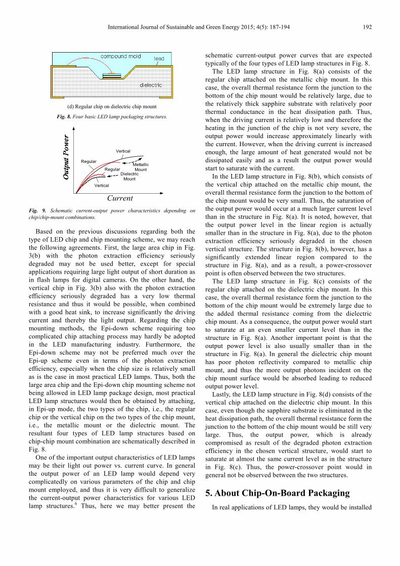
(d) Regular chip on dielectric chip mount
Fig. 8. Four basic LED lamp packaging structures.
Dielectric
Mount
Mettallic
Mount
Regular
Regular
Vertical
Vertical
Current Fig. 9. Schematic current-output power characteristics depending on
chip/chip-mount combinations.
Based on the previous discussions regarding both the
type of LED chip and chip mounting scheme, we may reach
the following agreements. First, the large area chip in Fig.
3(b) with the photon extraction efficiency seriously
degraded may not be used better, except for special
applications requiring large light output of short duration as
in flash lamps for digital cameras. On the other hand, the
vertical chip in Fig. 3(b) also with the photon extraction
efficiency seriously degraded has a very low thermal
resistance and thus it would be possible, when combined
with a good heat sink, to increase significantly the driving
current and thereby the light output. Regarding the chip
mounting methods, the Epi-down scheme requiring too
complicated chip attaching process may hardly be adopted
in the LED manufacturing industry. Furthermore, the
Epi-down scheme may not be preferred much over the
Epi-up scheme even in terms of the photon extraction
efficiency, especially when the chip size is relatively small
as is the case in most practical LED lamps. Thus, both the
large area chip and the Epi-down chip mounting scheme not
being allowed in LED lamp package design, most practical
LED lamp structures would then be obtained by attaching,
in Epi-up mode, the two types of the chip, i.e., the regular
chip or the vertical chip on the two types of the chip mount,
i.e., the metallic mount or the dielectric mount. The
resultant four types of LED lamp structures based on
chip-chip mount combination are schematically described in
Fig. 8.
One of the important output characteristics of LED lamps
may be their light out power vs. current curve. In general
the output power of an LED lamp would depend very
complicatedly on various parameters of the chip and chip
mount employed, and thus it is very difficult to generalize
the current-output power characteristics for various LED
lamp structures.6 Thus, here we may better present the
schematic current-output power curves that are expected
typically of the four types of LED lamp structures in Fig. 8.
The LED lamp structure in Fig. 8(a) consists of the
regular chip attached on the metallic chip mount. In this
case, the overall thermal resistance form the junction to the
bottom of the chip mount would be relatively large, due to
the relatively thick sapphire substrate with relatively poor
thermal conductance in the heat dissipation path. Thus,
when the driving current is relatively low and therefore the
heating in the junction of the chip is not very severe, the
output power would increase approximately linearly with
the current. However, when the driving current is increased
enough, the large amount of heat generated would not be
dissipated easily and as a result the output power would
start to saturate with the current.
In the LED lamp structure in Fig. 8(b), which consists of
the vertical chip attached on the metallic chip mount, the
overall thermal resistance form the junction to the bottom of
the chip mount would be very small. Thus, the saturation of
the output power would occur at a much larger current level
than in the structure in Fig. 8(a). It is noted, however, that
the output power level in the linear region is actually
smaller than in the structure in Fig. 8(a), due to the photon
extraction efficiency seriously degraded in the chosen
vertical structure. The structure in Fig. 8(b), however, has a
significantly extended linear region compared to the
structure in Fig. 8(a), and as a result, a power-crossover
point is often observed between the two structures.
The LED lamp structure in Fig. 8(c) consists of the
regular chip attached on the dielectric chip mount. In this
case, the overall thermal resistance form the junction to the
bottom of the chip mount would be extremely large due to
the added thermal resistance coming from the dielectric
chip mount. As a consequence, the output power would start
to saturate at an even smaller current level than in the
structure in Fig. 8(a). Another important point is that the
output power level is also usually smaller than in the
structure in Fig. 8(a). In general the dielectric chip mount
has poor photon reflectivity compared to metallic chip
mount, and thus the more output photons incident on the
chip mount surface would be absorbed leading to reduced
output power level.
Lastly, the LED lamp structure in Fig. 8(d) consists of the
vertical chip attached on the dielectric chip mount. In this
case, even though the sapphire substrate is eliminated in the
heat dissipation path, the overall thermal resistance form the
junction to the bottom of the chip mount would be still very
large. Thus, the output power, which is already
compromised as result of the degraded photon extraction
efficiency in the chosen vertical structure, would start to
saturate at almost the same current level as in the structure
in Fig. 8(c). Thus, the power-crossover point would in
general not be observed between the two structures.
5. About Chip-On-Board Packaging
In real applications of LED lamps, they would be installed

193 Song Jae Lee: Basic Guidelines for LED Lamp Package Design
often on a special printed circuit board (PCB) called the
metal core printed circuit board (MCPCB). The MCPCB with
improved thermal characteristics would help not only
increase per-unit output power but also stabilize the various
LED output characteristics, such as the spectrum distribution
and reliability. Fig. 10(a) shows a unit LED lamp put on the
MCPCB. Considering only the thermal characteristics,
however, it would be much more helpful to install LED chips
directly on PCB (COB: chip on board) as shown in Fig. 10(b).
Since the PCBs on which LED chips are installed are usually
much thicker and wider than the chip mounts in unit LED
lamps and thus have much larger heat capacity compared to
the chip mount. Thus the direct attachment of the LED chip
on PCBs would lead to drastically improved output power
and stabilized output characteristics.
(a) Unit LED lamp on PCB
(b)LED chip on PCB (Chip-On-Board)
Fig. 10. Two different approaches to implement LED lamps on PCB.
It is noted, however, that the COB scheme may not be
practical enough to be adopted extensively in the LED industry
for various reasons. First the PCB on which LED chips are
installed, possibly with other electrical or mechanical
components, will have a shape, size, or design that may in
general be widely different depending on the particular
application. As a consequence, it would be extremely difficult
or expensive to automatize, on this type of nonstandard PCBs,
the various LED lamp manufacturing processes, such as chip
attachment and encapsulation with molding compound.
Similarly the testing of the each LED lamp for the important
output characteristics, such as the output power, beam pattern,
spectrum, and reliability cannot be easily automatized on the
nonstandard PCB. Furthermore, if any of the LED lamps on
the PCB fails to meet any of the various specifications required
in the particular application, it would be very difficult or nearly
impossible to repair or replace the failed one that has been
molded strongly on the PCB.
On the other hand, in the case of the unit LED lamp
installed on the PCB as shown in Fig. 10(a), all the
manufacturing processes would be performed on standard
lead frames, whose shape, size, or design would be
determined independently of the particular applications, and
would easily be automatized. The resultant uniform unit LED
lamps of the same shape and design would then be tested
using the standard and automatized testing procedures. Lastly
only the unit LED lamps meeting all the required
specifications would be installed on the PCB and be replaced
quite easily, if any problem occurs after installment.
6. Conclusion
(a) Chip mount without isolating inter-walls
(b) Chip mount with isolating inter-walls
Fig. 11. Multi-Chip integration schemes.
Using Monte Carlo photon simulation method, the
performance of the regular chip, vertical chip, and large area
chip are analyzed and compared in terms of the photon
extraction efficiency. In addition, the Epi-Up and Epi-Down
chip-mounting schemes are analyzed and compared in terms
of both the photon extraction efficiency and the difficulties of
implementation. Based on the results of the analysis, we have
established the basic guidelines for the LED lamp package
design as follows:
� LED chips with chip area considerably larger than about
mm µµ 300300 × have the photon extraction efficiency
seriously degraded. Increasing the driving current by
more than proportionally to increased chip area in order
to compensate degraded photon extraction efficiency,
would inevitably lead to junction temperature rise,
which in turn would tend to decrease even the internal
quantum efficiency too. Thus, the large area chips are in
general not desired, except for special applications
requiring large output power for a short duration of time.
� The approach to increase the output power or photon
flux density by integrating multiple chips in one
package as shown in Fig. 11(a) would also suffer from
the degradation of the photon extraction efficiency as a
result of the significant optical coupling between
neighboring chips. In order to eliminate the in-between
optical coupling, the chip mounts with isolating
inter-walls as shown in Fig. 11(b) should be used.
� The regular chip has higher photon extraction efficiency
than the vertical chip, as a compensation for the
increased thermal resistance. It is always preferred over
the vertical chip in applications requiring low output
power that is to be achieved with minimal heating.
� The vertical chip has a much lower thermal resistance
than the regular chip, as a compensation for the

International Journal of Sustainable and Green Energy 2015; 4(5): 187-194 194
degraded photon extraction efficiency. In order to fully
exploit its thermal potential for increasing the driving
current and thereby output power, it should be mounted
on metallic chip mounts with improved heat sinking
capacity.
� Dielectric chip mounts with a larger thermal resistance
also have usually a poor photon reflectivity leading to
significant optical loss, and therefore they would not in
general be suited for applications requiring large output
power. Especially it is not very sensible to attach the
vertical chip on the dielectric chip mount since the
approach leads to both poor efficiency and poor thermal
behavior.
� The Epi-down chip mounting scheme requires a chip
attachment process that is so delicate that it can hardly
be adopted in the LED industry. Furthermore, it is not
preferred over the more conventional Epi-up scheme
even in terms of the photon extraction efficiency, when
the LED chip has a smaller area than about
mm µµ 300300 × .
� The COB scheme, despite the advantages of increasing
output power and better stabilizing output
characteristics, cannot be used extensively in the LED
industry due to the difficulties both in implementing it
and in replacing the failed LED lamps.
References
[1] Y. Li, W. Zhao, Y. Xia, M. Zhu, J. Senawiratne, T. Detchprohm, E. F. Shubert, and C. Wetzel, “Temperature dependence of the quantum efficiency in green light emitting diode dies”, Phys. Stat. Sol. (c) vol. 4, pp. 2784-2787, 2007.
[2] T. Mukai, M. Yamad, and S. Nakmura,, “InGaN-based uv/blue/green/amber/red LEDs”, Proc. SPIE, vol. 3621, pp. 2-14, San Jose, January 1999.
[3] S. J. Lee, “Analysis of light-emitting diodes by Monte Carlo photon simulation”, Appl. Opt., vol. 40, pp. 1427-1437, 2001.
[4] S. J. Lee, “Study of photon extraction efficiency in InGaN light-emitting diodes depending on chip structures and chip-mount schemes”, SPIE. Opt. Eng., vol. 45, pp. 1/14601-14/14601, 2006.
[5] S. J. Lee, “Electrode design for InGaA/Sapphire LED’s based on multiple thin ohmic metal patches”, Proc. SPIE, vol. 5530, pp. 339-346, Denver, Aug. 2004.
[6] D. W. Hong, J. K. Yoo, J. M. Kim, M. J. Yoon, and S. J. Lee, “Analysis of the optical effect of the substrate removal and chip-mount type on light output power characteristics in InGaN/Sapphire LEDs,” Hankook Kwanghak Hoeji (Korean J. of Opt. Photon.) vol 19, pp. 381-385, 2008.