Embed Size (px)
Citation preview
3685 Richmond Road, Suite 500, Ottawa, ON K2H 5B7 Canada – Tel: 613-829-0414www.chipworks.com
Basic Functional Analysis
Sample Report

Some of the information in this report may be covered by patents, mask, and/or copyright protection. This report should not be taken as an inducement to infringe on these rights.
© 2009 Chipworks Inc.
This report is provided exclusively for the use of the purchasing organization. It can be freely copied and distributed within the purchasing organization, conditional upon the accompanying Chipworks accreditation remaining attached.
Distribution of the entire report outside of the purchasing organization is strictly forbidden. The use of portions of the document for the support of the purchasing organization’s corporate interest (e.g., licensing or marketing activities) is permitted, as defined by the fair use provisions of the copyright act. Accreditation to Chipworks must be attached to any portion of the reproduced information.
FAR-0906-90113685CYBT
Revision 1.0 Published: July 16, 2009
Basic Functional AnalysisSample Report
Table of Contents
1 Overview1.1 List of Figures1.2 List of Tables1.3 Introduction1.4 Device Summary1.5 Observed Critical Dimensions
2 Device Identification2.1 Downstream2.2 Package2.3 Die
3 Process3.1 Overview
4 Functional Layout Analysis4.1 Overview4.2 Functional Block Measurements
5 Estimated Costing 5.1 Manufacturing Cost Analysis
6 Statement of Measurement Uncertainty and Scope Variation
About Chipworks
Basic Functional AnalysisSample Report
Basic Functional Analysis – Sample ReportOverview 1-1
1 Overview
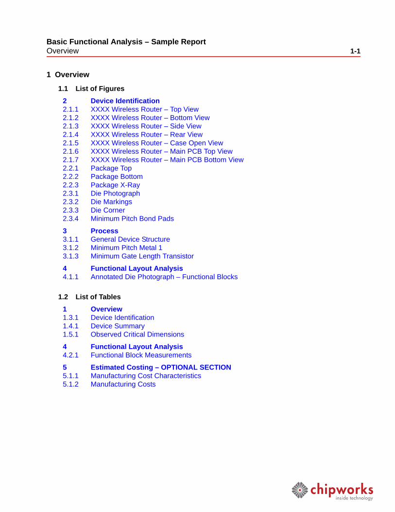
1.1 List of Figures2 Device Identification2.1.1 XXXX Wireless Router – Top View2.1.2 XXXX Wireless Router – Bottom View2.1.3 XXXX Wireless Router – Side View2.1.4 XXXX Wireless Router – Rear View2.1.5 XXXX Wireless Router – Case Open View2.1.6 XXXX Wireless Router – Main PCB Top View2.1.7 XXXX Wireless Router – Main PCB Bottom View2.2.1 Package Top2.2.2 Package Bottom2.2.3 Package X-Ray2.3.1 Die Photograph2.3.2 Die Markings2.3.3 Die Corner2.3.4 Minimum Pitch Bond Pads
3 Process3.1.1 General Device Structure3.1.2 Minimum Pitch Metal 13.1.3 Minimum Gate Length Transistor
4 Functional Layout Analysis4.1.1 Annotated Die Photograph – Functional Blocks
1.2 List of Tables1 Overview1.3.1 Device Identification1.4.1 Device Summary1.5.1 Observed Critical Dimensions
4 Functional Layout Analysis4.2.1 Functional Block Measurements
5 Estimated Costing – OPTIONAL SECTION5.1.1 Manufacturing Cost Characteristics5.1.2 Manufacturing Costs
Basic Functional Analysis – Sample ReportOverview 1-2
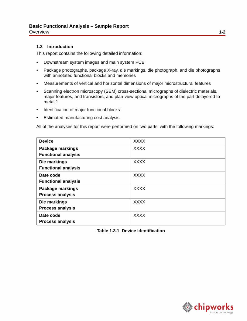
1.3 IntroductionThis report contains the following detailed information:
• Downstream system images and main system PCB
• Package photographs, package X-ray, die markings, die photograph, and die photographs with annotated functional blocks and memories
• Measurements of vertical and horizontal dimensions of major microstructural features
• Scanning electron microscopy (SEM) cross-sectional micrographs of dielectric materials, major features, and transistors, and plan-view optical micrographs of the part delayered to metal 1
• Identification of major functional blocks
• Estimated manufacturing cost analysis
All of the analyses for this report were performed on two parts, with the following markings:
Table 1.3.1 Device Identification1.3.1 Device Identification
Table 1.3.1 Device Identification
Device XXXXPackage markingsFunctional analysis
XXXX
Die markingsFunctional analysis
XXXX
Date codeFunctional analysis
XXXX
Package markingsProcess analysis
XXXX
Die markingsProcess analysis
XXXX
Date codeProcess analysis
XXXX
Basic Functional Analysis – Sample ReportOverview 1-3
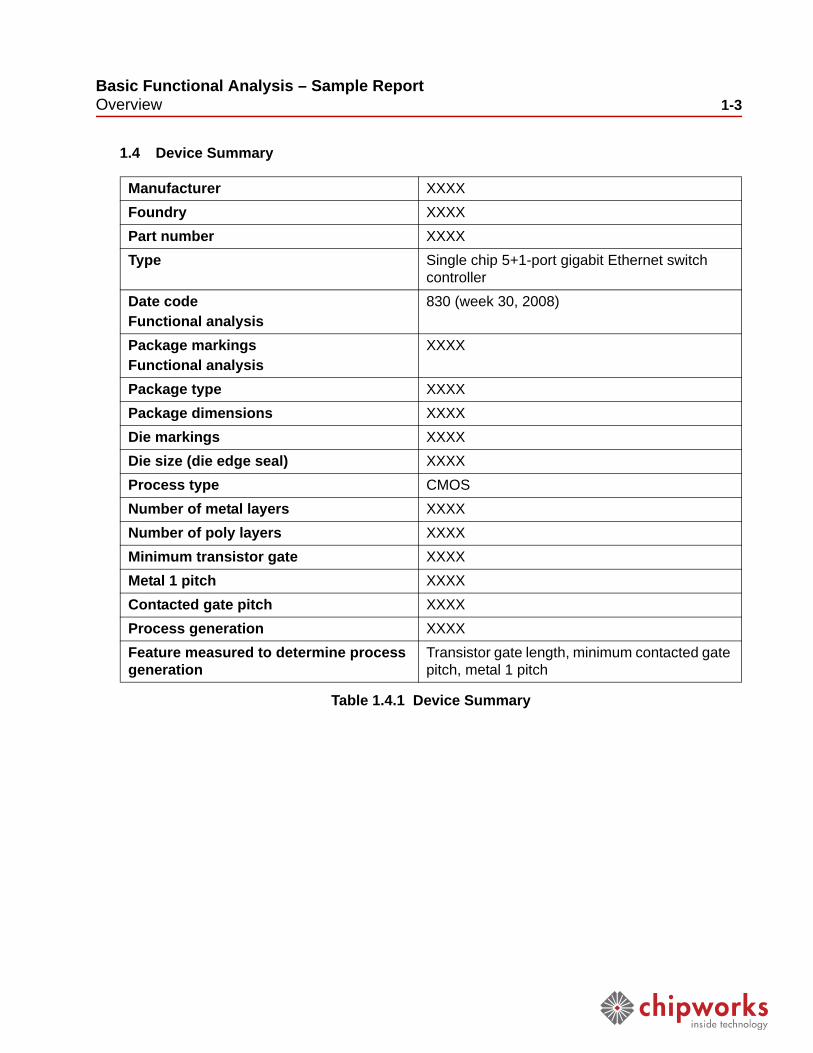
1.4 Device SummaryTable 1.4.1 Device Summary
1.4.1 Device Summary
Table 1.4.1 Device Summary
Manufacturer XXXXFoundry XXXXPart number XXXXType Single chip 5+1-port gigabit Ethernet switch
controllerDate codeFunctional analysis
830 (week 30, 2008)
Package markingsFunctional analysis
XXXX
Package type XXXXPackage dimensions XXXXDie markings XXXXDie size (die edge seal) XXXXProcess type CMOSNumber of metal layers XXXXNumber of poly layers XXXXMinimum transistor gate XXXXMetal 1 pitch XXXXContacted gate pitch XXXXProcess generation XXXXFeature measured to determine processgeneration
Transistor gate length, minimum contacted gate pitch, metal 1 pitch
Basic Functional Analysis – Sample ReportOverview 1-4
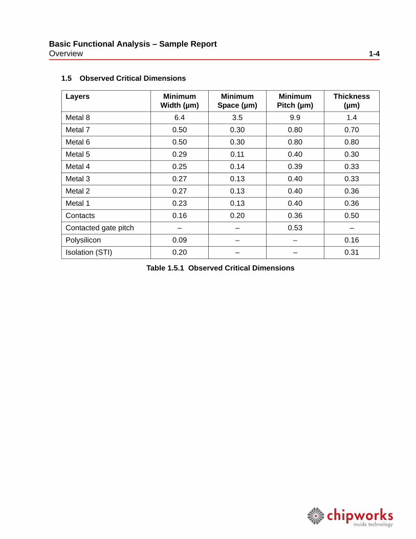
1.5 Observed Critical DimensionsTable 1.5.1 Observed Critical Dimensions
1.5.1 Observed Critical Dimensions
Table 1.5.1 Observed Critical Dimensions
Layers MinimumWidth (µm)
MinimumSpace (µm)
MinimumPitch (µm)
Thickness(µm)
Metal 8 6.4 3.5 9.9 1.4Metal 7 0.50 0.30 0.80 0.70Metal 6 0.50 0.30 0.80 0.80Metal 5 0.29 0.11 0.40 0.30Metal 4 0.25 0.14 0.39 0.33Metal 3 0.27 0.13 0.40 0.33Metal 2 0.27 0.13 0.40 0.36Metal 1 0.23 0.13 0.40 0.36Contacts 0.16 0.20 0.36 0.50Contacted gate pitch – – 0.53 –Polysilicon 0.09 – – 0.16Isolation (STI) 0.20 – – 0.31
Basic Functional Analysis – Sample ReportDevice Identification 2-1
2 Device Identification
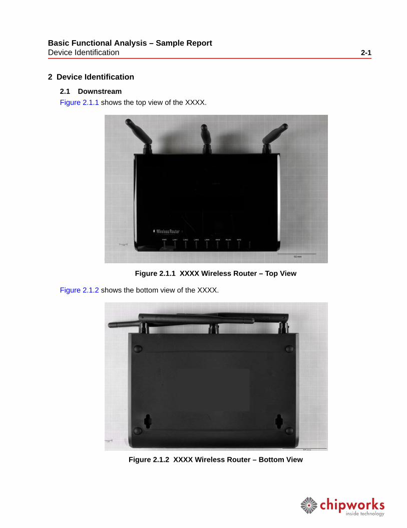
2.1 DownstreamFigure 2.1.1 shows the top view of the XXXX.
Figure 2.1.1XXXX Wireless Router – Top ViewFigure 2.1.1 XXXX Wireless Router – Top View
Figure 2.1.1 XXXX Wireless Router – Top View
Figure 2.1.2 shows the bottom view of the XXXX.Figure 2.1.2XXXX Wireless Router – Bottom View
Figure 2.1.2 XXXX Wireless Router – Bottom View
Figure 2.1.2 XXXX Wireless Router – Bottom View
50 mm
50 mm
Basic Functional Analysis – Sample ReportDevice Identification 2-2
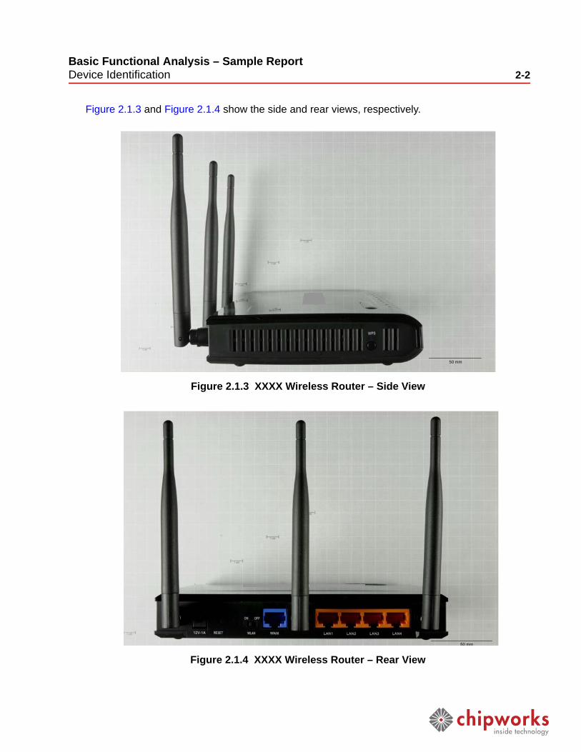
Figure 2.1.3 and Figure 2.1.4 show the side and rear views, respectively.Figure 2.1.3XXXX Wireless Router – Side View
Figure 2.1.3 XXXX Wireless Router – Side View
Figure 2.1.3 XXXX Wireless Router – Side ViewFigure 2.1.4XXXX Wireless Router – Rear ViewFigure 2.1.4 XXXX Wireless Router – Rear View
Figure 2.1.4 XXXX Wireless Router – Rear View
50 mm
50 mm
Basic Functional Analysis – Sample ReportDevice Identification 2-3
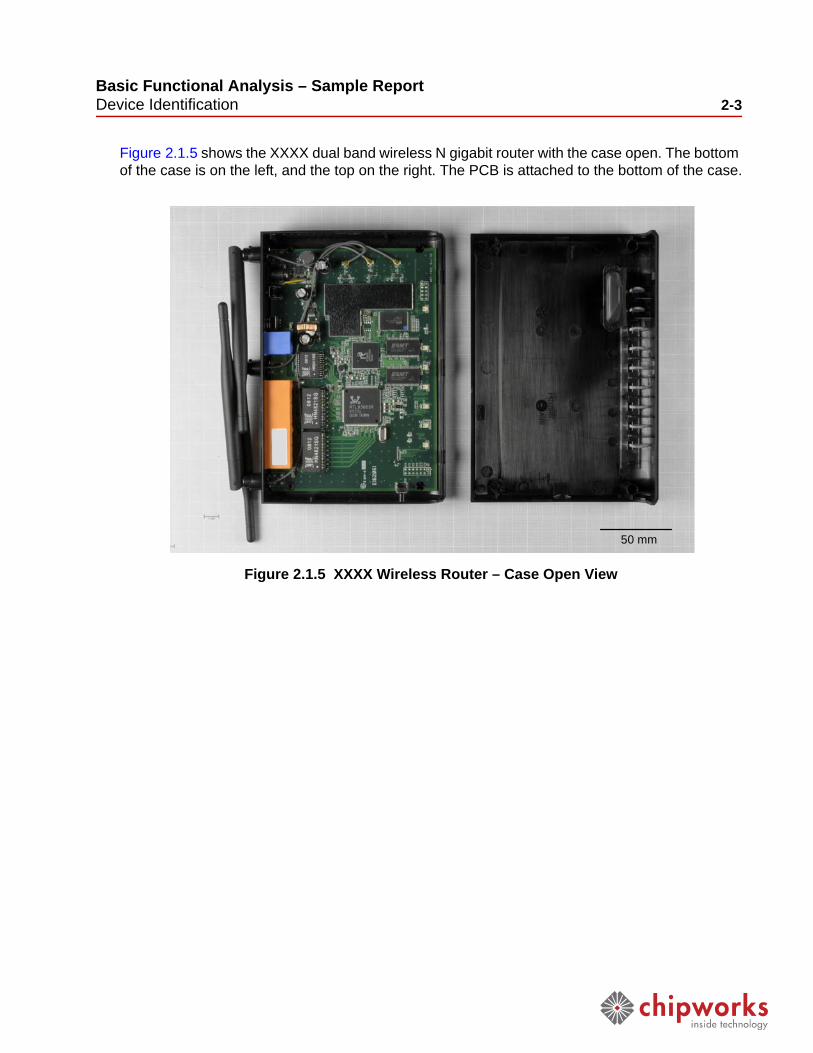
Figure 2.1.5 shows the XXXX dual band wireless N gigabit router with the case open. The bottom of the case is on the left, and the top on the right. The PCB is attached to the bottom of the case.
Figure 2.1.5XXXX Wireless Router – Case Open ViewFigure 2.1.5 XXXX Wireless Router – Case Open View
Figure 2.1.5 XXXX Wireless Router – Case Open View
50 mm
Basic Functional Analysis – Sample ReportDevice Identification 2-4
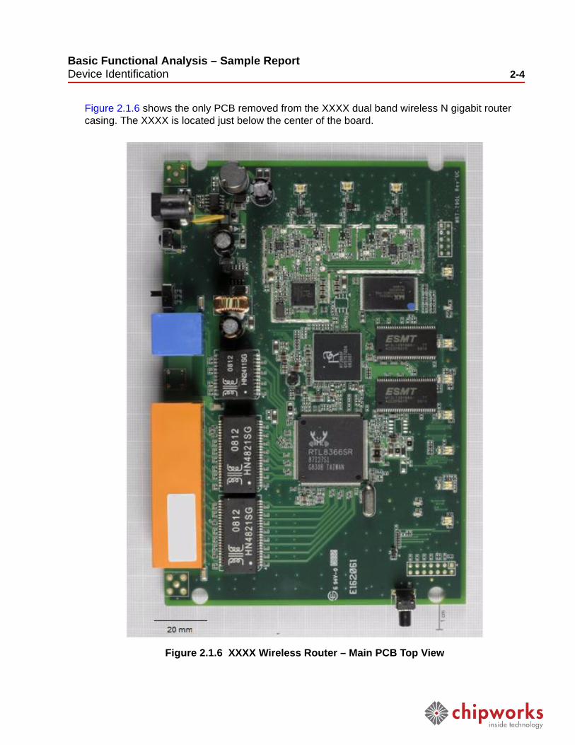
Figure 2.1.6 shows the only PCB removed from the XXXX dual band wireless N gigabit router casing. The XXXX is located just below the center of the board.
Figure 2.1.6XXXX Wireless Router – Main PCB Top ViewFigure 2.1.6 XXXX Wireless Router – Main PCB Top View
Figure 2.1.6 XXXX Wireless Router – Main PCB Top View
Basic Functional Analysis – Sample ReportDevice Identification 2-5
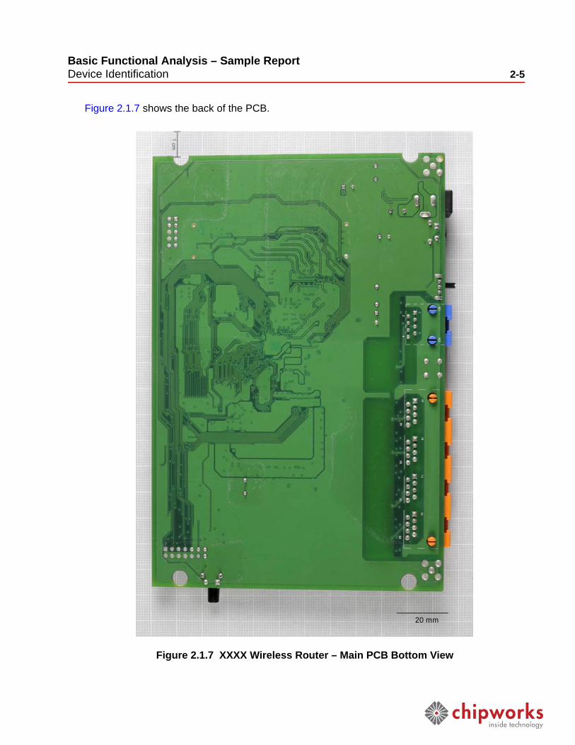
Figure 2.1.7 shows the back of the PCB.Figure 2.1.7XXXX Wireless Router – Main PCB Bottom ViewFigure 2.1.7 XXXX Wireless Router – Main PCB Bottom View
Figure 2.1.7 XXXX Wireless Router – Main PCB Bottom View
20 mm
Basic Functional Analysis – Sample ReportDevice Identification 2-6
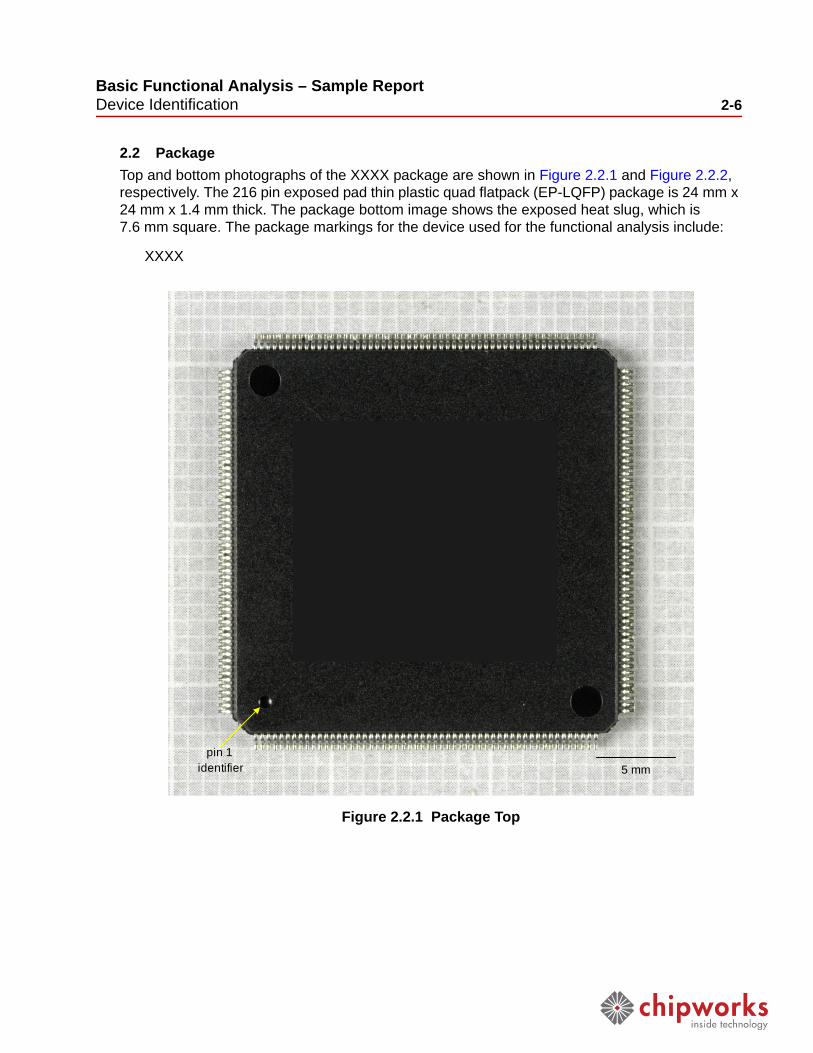
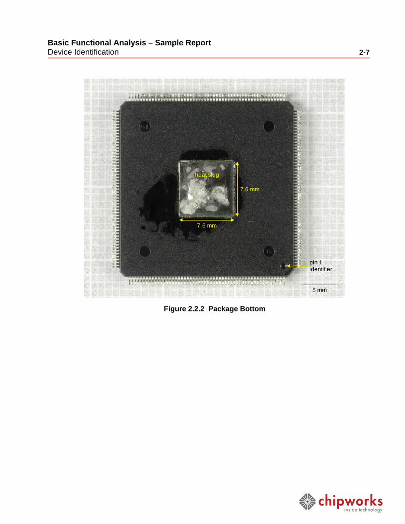
2.2 PackageTop and bottom photographs of the XXXX package are shown in Figure 2.2.1 and Figure 2.2.2, respectively. The 216 pin exposed pad thin plastic quad flatpack (EP-LQFP) package is 24 mm x 24 mm x 1.4 mm thick. The package bottom image shows the exposed heat slug, which is 7.6 mm square. The package markings for the device used for the functional analysis include:
XXXXFigure 2.2.1Package TopFigure 2.2.1 Package Top
Figure 2.2.1 Package Top
5 mmpin 1
identifier
Basic Functional Analysis – Sample ReportDevice Identification 2-7
Figure 2.2.2Package BottomFigure 2.2.2 Package Bottom
Figure 2.2.2 Package Bottom
5 mm
heat slug
7.6 mm
7.6 mm
pin 1identifier
Basic Functional Analysis – Sample ReportDevice Identification 2-8
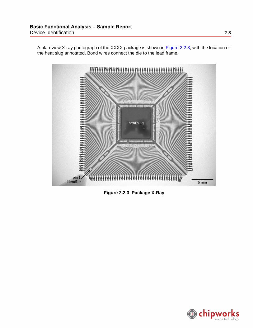
A plan-view X-ray photograph of the XXXX package is shown in Figure 2.2.3, with the location of the heat slug annotated. Bond wires connect the die to the lead frame.
Figure 2.2.3Package X-RayFigure 2.2.3 Package X-Ray
Figure 2.2.3 Package X-Ray
5 mm
heat slug
pin 1identifier
Basic Functional Analysis – Sample ReportDevice Identification 2-9
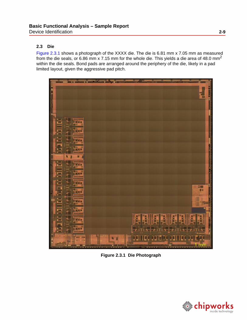
2.3 DieFigure 2.3.1 shows a photograph of the XXXX die. The die is 6.81 mm x 7.05 mm as measured from the die seals, or 6.86 mm x 7.15 mm for the whole die. This yields a die area of 48.0 mm2
within the die seals. Bond pads are arranged around the periphery of the die, likely in a pad limited layout, given the aggressive pad pitch.
Figure 2.3.1Die PhotographFigure 2.3.1 Die Photograph
Figure 2.3.1 Die Photograph
Basic Functional Analysis – Sample ReportDevice Identification 2-10
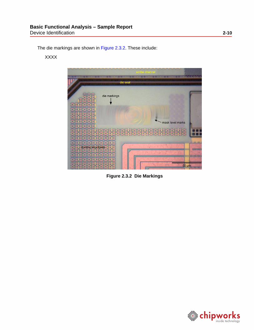
The die markings are shown in Figure 2.3.2. These include:
XXXXFigure 2.3.2Die Markings
Figure 2.3.2 Die Markings
Figure 2.3.2 Die Markings
Basic Functional Analysis – Sample ReportDevice Identification 2-11
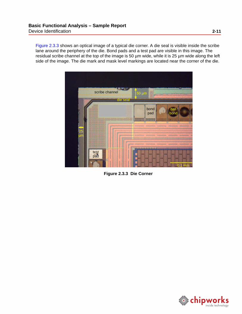
Figure 2.3.3 shows an optical image of a typical die corner. A die seal is visible inside the scribe lane around the periphery of the die. Bond pads and a test pad are visible in this image. The residual scribe channel at the top of the image is 50 µm wide, while it is 25 µm wide along the left side of the image. The die mark and mask level markings are located near the corner of the die.
Figure 2.3.3Die CornerFigure 2.3.3 Die Corner
Figure 2.3.3 Die Corner
0.1 mm
die seal
bondpad
testpad
ballbond
scribe channel 50 µm
25µm
Basic Functional Analysis – Sample ReportDevice Identification 2-12
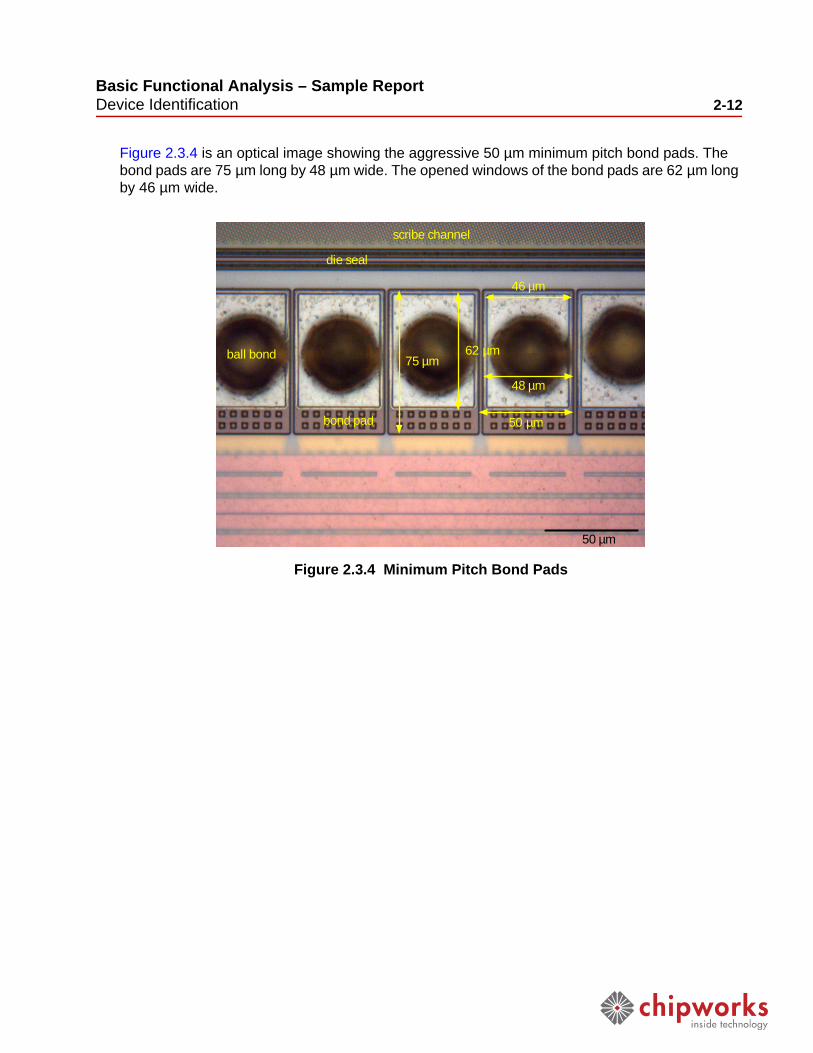
Figure 2.3.4 is an optical image showing the aggressive 50 µm minimum pitch bond pads. The bond pads are 75 µm long by 48 µm wide. The opened windows of the bond pads are 62 µm long by 46 µm wide.
Figure 2.3.4Minimum Pitch Bond PadsFigure 2.3.4 Minimum Pitch Bond Pads
Figure 2.3.4 Minimum Pitch Bond Pads
50 µm
scribe channel
die seal
ball bond
bond pad
75 µm
48 µm
50 µm
62 µm
46 µm
Basic Functional Analysis – Sample ReportProcess 3-1
3 Process
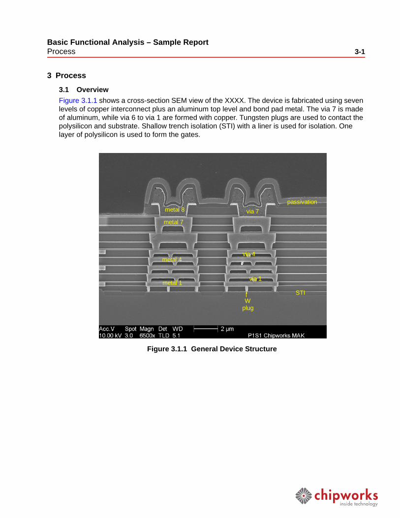
3.1 OverviewFigure 3.1.1 shows a cross-section SEM view of the XXXX. The device is fabricated using seven levels of copper interconnect plus an aluminum top level and bond pad metal. The via 7 is made of aluminum, while via 6 to via 1 are formed with copper. Tungsten plugs are used to contact the polysilicon and substrate. Shallow trench isolation (STI) with a liner is used for isolation. One layer of polysilicon is used to form the gates.
Figure 3.1.1General Device StructureFigure 3.1.1 General Device Structure
Figure 3.1.1 General Device Structure
passivation
STImetal 1
metal 4
metal 8
metal 7
Wplug
via 1
via 4
via 7
Basic Functional Analysis – Sample ReportProcess 3-2
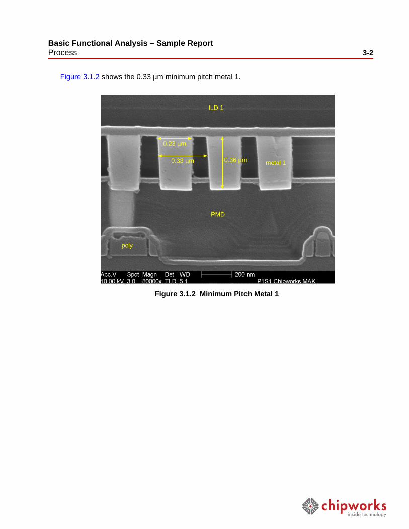
Figure 3.1.2 shows the 0.33 µm minimum pitch metal 1.Figure 3.1.2Minimum Pitch Metal 1Figure 3.1.2 Minimum Pitch Metal 1
Figure 3.1.2 Minimum Pitch Metal 1
0.23 µm
0.33 µm 0.36 µm metal 1
PMD
poly
ILD 1
Basic Functional Analysis – Sample ReportProcess 3-3
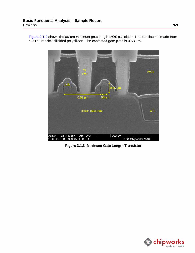
Figure 3.1.3 shows the 90 nm minimum gate length MOS transistor. The transistor is made from a 0.16 µm thick silicided polysilicon. The contacted gate pitch is 0.53 µm.
Figure 3.1.3Minimum Gate Length TransistorFigure 3.1.3 Minimum Gate Length Transistor
Figure 3.1.3 Minimum Gate Length Transistor
0.53 µm 90 nm
poly
Wplug PMD
STI
0.16 µm
silicon substrate
Basic Functional Analysis – Sample ReportFunctional Layout Analysis 4-1
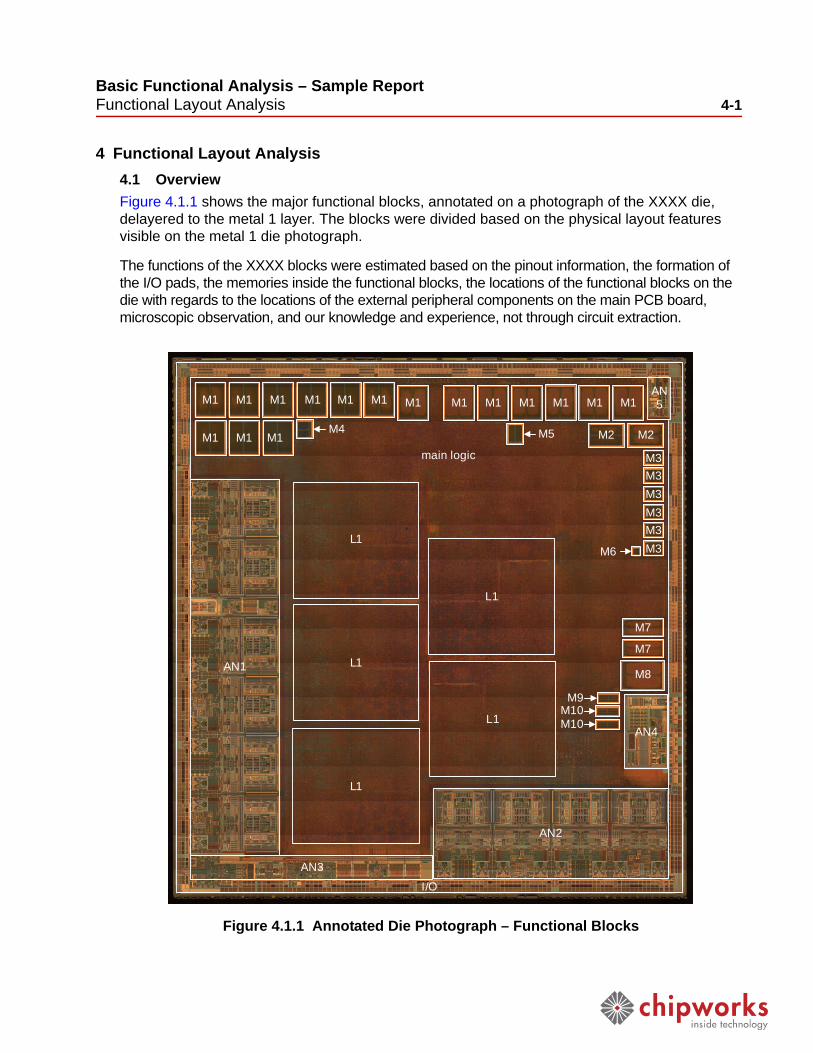
4 Functional Layout Analysis4.1 OverviewFigure 4.1.1 shows the major functional blocks, annotated on a photograph of the XXXX die, delayered to the metal 1 layer. The blocks were divided based on the physical layout features visible on the metal 1 die photograph.
The functions of the XXXX blocks were estimated based on the pinout information, the formation of the I/O pads, the memories inside the functional blocks, the locations of the functional blocks on the die with regards to the locations of the external peripheral components on the main PCB board, microscopic observation, and our knowledge and experience, not through circuit extraction.
Figure 4.1.1Annotated Die Photograph – Functional BlocksFigure 4.1.1 Annotated Die Photograph – Functional Blocks
Figure 4.1.1 Annotated Die Photograph – Functional Blocks
AN1
AN2
AN3
AN4
AN 5M1
M1
M1
M1
M1
M1
M1 M1 M1 M1 M1 M1 M1 M1 M1 M1
M2 M2
M3M3M3M3M3M3
M4 M5
M6
M7
M7
M8
M9M10M10
main logic
I/O
L1
L1
L1
L1
L1
Basic Functional Analysis – Sample ReportFunctional Layout Analysis 4-2
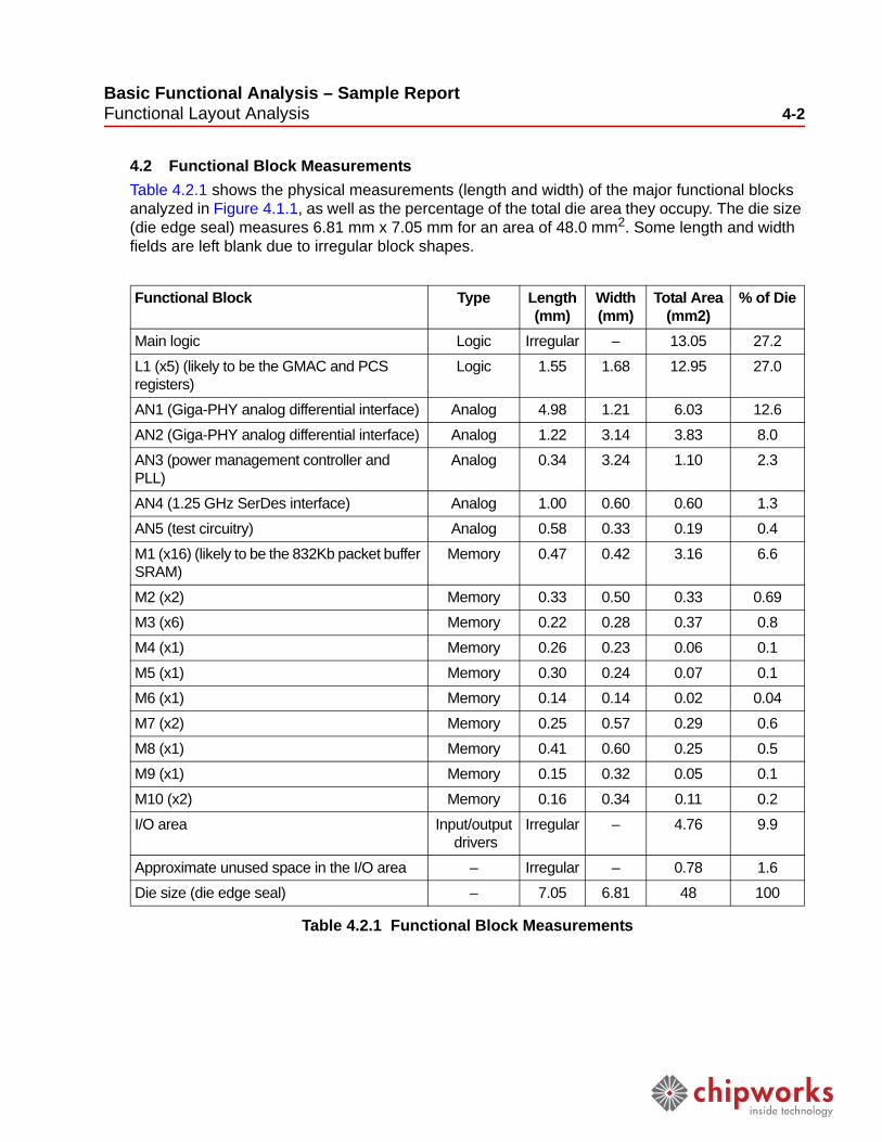
4.2 Functional Block MeasurementsTable 4.2.1 shows the physical measurements (length and width) of the major functional blocks analyzed in Figure 4.1.1, as well as the percentage of the total die area they occupy. The die size (die edge seal) measures 6.81 mm x 7.05 mm for an area of 48.0 mm2. Some length and width fields are left blank due to irregular block shapes.
Table 4.2.1 Functional Block Measurements4.2.1 Functional Block Measurements
Table 4.2.1 Functional Block Measurements
Functional Block Type Length(mm)
Width(mm)
Total Area(mm2)
% of Die
Main logic Logic Irregular – 13.05 27.2
L1 (x5) (likely to be the GMAC and PCSregisters)
Logic 1.55 1.68 12.95 27.0
AN1 (Giga-PHY analog differential interface) Analog 4.98 1.21 6.03 12.6
AN2 (Giga-PHY analog differential interface) Analog 1.22 3.14 3.83 8.0AN3 (power management controller andPLL)
Analog 0.34 3.24 1.10 2.3
AN4 (1.25 GHz SerDes interface) Analog 1.00 0.60 0.60 1.3
AN5 (test circuitry) Analog 0.58 0.33 0.19 0.4
M1 (x16) (likely to be the 832Kb packet buffer SRAM)
Memory 0.47 0.42 3.16 6.6
M2 (x2) Memory 0.33 0.50 0.33 0.69M3 (x6) Memory 0.22 0.28 0.37 0.8
M4 (x1) Memory 0.26 0.23 0.06 0.1
M5 (x1) Memory 0.30 0.24 0.07 0.1M6 (x1) Memory 0.14 0.14 0.02 0.04
M7 (x2) Memory 0.25 0.57 0.29 0.6
M8 (x1) Memory 0.41 0.60 0.25 0.5M9 (x1) Memory 0.15 0.32 0.05 0.1
M10 (x2) Memory 0.16 0.34 0.11 0.2
I/O area Input/output drivers
Irregular – 4.76 9.9
Approximate unused space in the I/O area – Irregular – 0.78 1.6Die size (die edge seal) – 7.05 6.81 48 100
Basic Functional Analysis – Sample ReportEstimated Costing 5-1
5 Estimated Costing
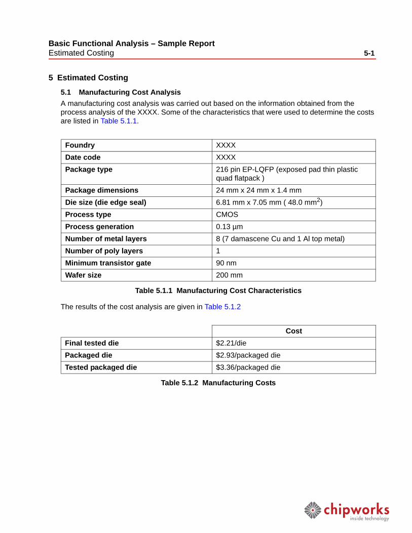
5.1 Manufacturing Cost AnalysisA manufacturing cost analysis was carried out based on the information obtained from the process analysis of the XXXX. Some of the characteristics that were used to determine the costs are listed in Table 5.1.1.
Table 5.1.1 Manufacturing Cost Characteristics5.1.1 Manufacturing Cost Characteristics
Table 5.1.1 Manufacturing Cost Characteristics
The results of the cost analysis are given in Table 5.1.2
Table 5.1.2 Manufacturing Costs5.1.2 Manufacturing Costs
Table 5.1.2 Manufacturing Costs
Foundry XXXXDate code XXXXPackage type 216 pin EP-LQFP (exposed pad thin plastic
quad flatpack )Package dimensions 24 mm x 24 mm x 1.4 mmDie size (die edge seal) 6.81 mm x 7.05 mm ( 48.0 mm2)Process type CMOSProcess generation 0.13 µmNumber of metal layers 8 (7 damascene Cu and 1 Al top metal)Number of poly layers 1Minimum transistor gate 90 nmWafer size 200 mm
CostFinal tested die $2.21/diePackaged die $2.93/packaged dieTested packaged die $3.36/packaged die
Basic Functional Analysis – Sample ReportStatement of Measurement Uncertainty and Scope Variation 6-1
6 Statement of Measurement Uncertainty and Scope Variation
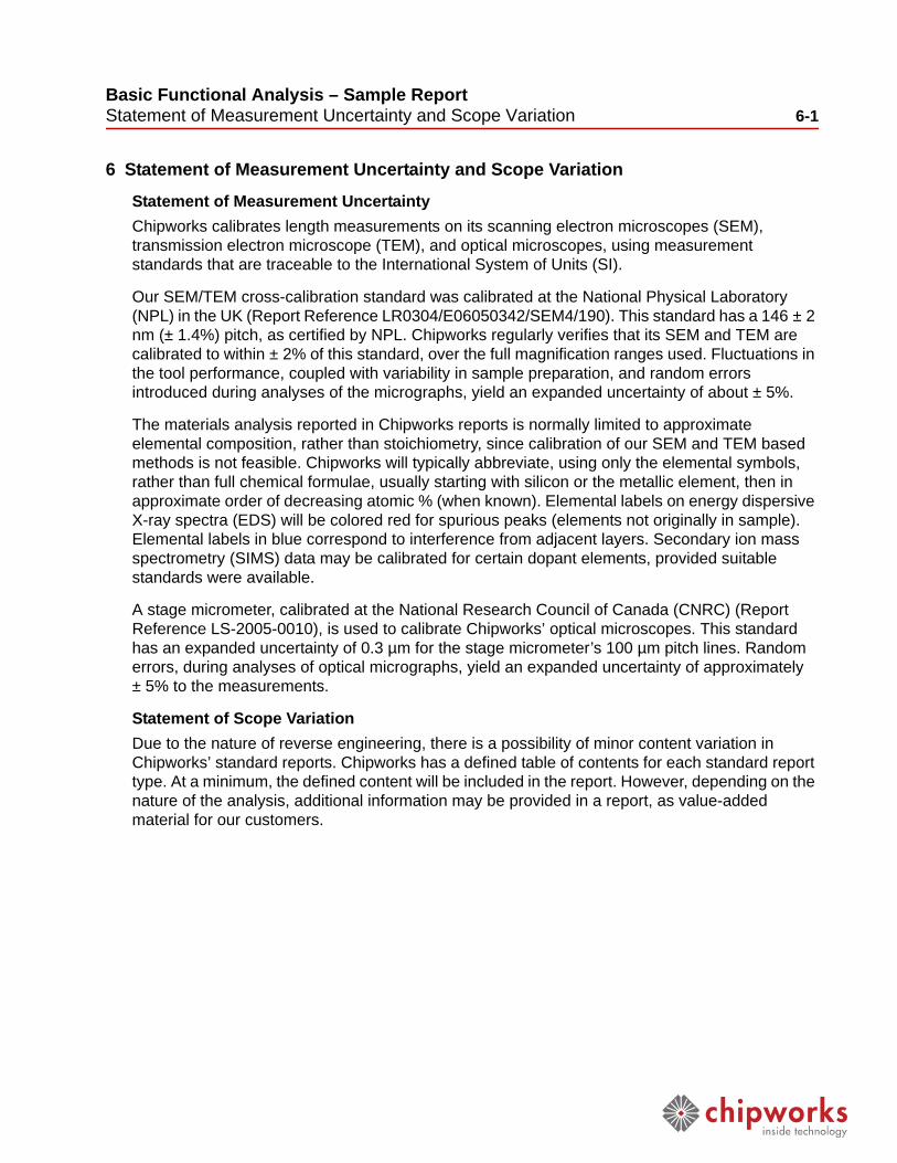
Statement of Measurement UncertaintyChipworks calibrates length measurements on its scanning electron microscopes (SEM), transmission electron microscope (TEM), and optical microscopes, using measurement standards that are traceable to the International System of Units (SI).
Our SEM/TEM cross-calibration standard was calibrated at the National Physical Laboratory (NPL) in the UK (Report Reference LR0304/E06050342/SEM4/190). This standard has a 146 ± 2 nm (± 1.4%) pitch, as certified by NPL. Chipworks regularly verifies that its SEM and TEM are calibrated to within ± 2% of this standard, over the full magnification ranges used. Fluctuations in the tool performance, coupled with variability in sample preparation, and random errors introduced during analyses of the micrographs, yield an expanded uncertainty of about ± 5%.
The materials analysis reported in Chipworks reports is normally limited to approximate elemental composition, rather than stoichiometry, since calibration of our SEM and TEM based methods is not feasible. Chipworks will typically abbreviate, using only the elemental symbols, rather than full chemical formulae, usually starting with silicon or the metallic element, then in approximate order of decreasing atomic % (when known). Elemental labels on energy dispersive X-ray spectra (EDS) will be colored red for spurious peaks (elements not originally in sample). Elemental labels in blue correspond to interference from adjacent layers. Secondary ion mass spectrometry (SIMS) data may be calibrated for certain dopant elements, provided suitable standards were available.
A stage micrometer, calibrated at the National Research Council of Canada (CNRC) (Report Reference LS-2005-0010), is used to calibrate Chipworks’ optical microscopes. This standard has an expanded uncertainty of 0.3 µm for the stage micrometer’s 100 µm pitch lines. Random errors, during analyses of optical micrographs, yield an expanded uncertainty of approximately± 5% to the measurements.
Statement of Scope VariationDue to the nature of reverse engineering, there is a possibility of minor content variation in Chipworks’ standard reports. Chipworks has a defined table of contents for each standard report type. At a minimum, the defined content will be included in the report. However, depending on the nature of the analysis, additional information may be provided in a report, as value-added material for our customers.

Basic Functional Analysis – Sample Report About Chipworks
About Chipworks Chipworks is the recognized leader in reverse engineering and patent infringement analysis of semiconductors and electronic systems. The company’s ability to analyze the circuitry and physical composition of these systems makes them a key partner in the success of the world’s largest semiconductor and microelectronics companies. Intellectual property groups and their legal counsel trust Chipworks for success in patent licensing and litigation – earning hundreds of millions of dollars in patent licenses, and saving as much in royalty payments. Research & Development and Product Management rely on Chipworks for success in new product design and launch, saving hundreds of millions of dollars in design, and earning even more through superior product design and faster launches.
Contact Chipworks To find out more information on this report, or any other reports in our library, please contact Chipworks at 1-613-829-0414.
Chipworks 3685 Richmond Road, Suite 500 Ottawa, Ontario K2H 5B7 Canada T 1-613-829-0414 F 1-613-829-0515 Web site: www.chipworks.com Email: [email protected]
Please send any feedback to [email protected]


![ANNUAL REPORT 2013eurireland.ie/assets/uploads/2017/05/annual_report_2013_final.pdf · 5b7\ca\U]f`YiaH\U][\XY]bv]f]bb. 2 Irish Research Council Annual Report 3 contents Foreword 5](https://img.pdfslide.us/doc/110x75/5fb7cd65b7e5c110843bf373/annual-report-5b7caufyiahuxybvfbb-2-irish-research-council-annual-report.jpg)