Embed Size (px)
Citation preview

Course Outline
Basic Concepts in RF Design
Low-Noise Amplifiers
Mixers
Oscillators
Phase-Locked Loops

General Considerations
Power Dissipation
Noise Figure
Linearity
Gain
Bandwidth
Input Matching (antenna-LNA matching)
in most receivers, the LNA consumes only a small fraction of the overall
power
the stronger trade off to address is between NF and input matching
As the first active stage of receivers, LNAs play a critical role
in the overall performance and their design is governed by a
trade off among the following parameters

General Considerations: Noise Figure
The LNA contributes 2 to 3 dB of the total RX noise figure (6 to 8 dB).
A noise figure of 2 dB with respect to a source impedance of 50Ω translates to:
an extremely low value.
V2n,in includes both the LNA
EIVN and EICN

Example of Metal Resistance and Noise Figure
A student lays out an LNA and connects its input to a pad through a metal line 200µm long. In order to minimize the input capacitance, the student chooses a widthof 0.5 µm for the line. Assuming a NF=2 dB for the LNA and a sheet resistance of
40 mΩ/ for the metal line, determine the overall NF (neglect the input-referrednoise current of the LNA).
The total input-referred noise voltage of the circuit inside the box is therefore equalto Vn,in
2+4kTRL. We thus write
Since NFLNA = 2 dB ≡ 1.58 and RL = (200/0.5) ×××× 40 mΩ/ = 16 Ω, we have
even small amounts of line or gate resistance can raise the NF of LNAs
considerably.

General Considerations: Linearity
In most applications, the LNA does not limit the linearity of the receiver,which is usually limited by the bandbase amplifiers or filters Linearityusually is not a concern for LNAs.
Exception: “full-duplex” systems
Leakages 1-3 and 1-2 ~ 1 to 2 dB
Leakage 2-3 ~ 50 dB
Ex: the PA produces an averagepower of +30 dBmthe LNAexperiments an interferer in the TXband of -20 dBm, much stronger thanthe detected signal the 1dBcompression point of LNA andsubsequent stages should beincreased .
Usually an off-chip filter is interposed between the LNA and mixer to remove the TXleakage.

General Considerations: Gain
LNA gain is a trade-off between low noise (large enough to minimize thenoise contribution of subsequent stages, specifically, thedownconversion mixer) and linearity
The noise and IP3 of the stage following the LNA are divided by different LNA gains
with input matching, Rin=RS α1=2Av1 assume αααα2=0

General Considerations: Bandwidth
An 802.11a LNA must achieve a -3-dB bandwidth from 5 GHz to 6 GHz. If the LNA incorporates a second-order LC tank as its load, what is the maximum allowable tank Q?
the fractional bandwidth of an LC tank is∆ω/ω0 = 1/Q
The minimum required 3dB bandwidth is∆ω=2ππππ ∙1 Ghz Q ≤ 5.5 GHz/1 GHz = 5.5.
The LNA must provide a relatively flat response for the frequency range ofinterest, preferably with less than 1 dB of gain variation.
The LNA -3-dB bandwidth must therefore be substantially larger than theactual band so that the roll-off at the edges remains below 1 dB.
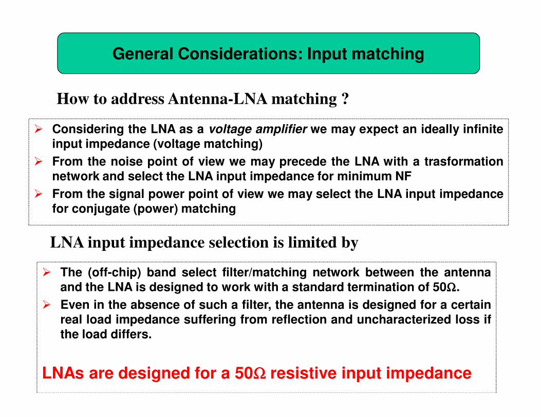
General Considerations: Input matching
Considering the LNA as a voltage amplifier we may expect an ideally infiniteinput impedance (voltage matching)
From the noise point of view we may precede the LNA with a trasformationnetwork and select the LNA input impedance for minimum NF
From the signal power point of view we may select the LNA input impedancefor conjugate (power) matching
How to address Antenna-LNA matching ?
LNA input impedance selection is limited by
The (off-chip) band select filter/matching network between the antennaand the LNA is designed to work with a standard termination of 50ΩΩΩΩ.
Even in the absence of such a filter, the antenna is designed for a certainreal load impedance suffering from reflection and uncharacterized loss ifthe load differs.
LNAs are designed for a 50ΩΩΩΩ resistive input impedance

Zin= 50 ΩΩΩΩ limits the choice of LNA topologies: we cannot begin with anarbitrary configuration, design it for NF and gain, and then decide how tocreate input matching.
Consider the case of a Common Source (CS) stage:
Example of typical parameters:
CF=10 fF, CL=30 fF, gmRD=4, RD=100ΩΩΩΩ , f=5Ghz ReYin=(7.8 kΩ)Ω)Ω)Ω)−−−−1111 very farfrom (50Ω)Ω)Ω)Ω)−−−−1111.... This is because CF introduces little feedback at this frequency.
The gate-drain overlap capacitance (CF) allows creating a real part for inputmatching (for CF=0 ReYin=0)
General Considerations: Input matching

Resistive Termination for Matching
express the total output noise (at low frequencies) as:
Can we employ simple resistive termination at the input? three steps design:
(1) M1 and RD are selected to provide the required NF and gain
(2) RP = 50Ω is placed in parallel with the input so that
ReYin,p=ReYin+1/RP=(7.8 kΩ)Ω)Ω)Ω)−−−−1111++++(50Ω)-1 ~ 1/RP=(50Ω)-1
(3) an inductor (L1) is interposed between RS and the input to cancel ImZin.

Resistive Termination for Matching
RP increases the NF. For RP = RS, the NF exceeds 3 dB substantially.
LNA must provide a 50 ΩΩΩΩ input resistance without the thermal noise
of a physical 50 ΩΩΩΩ resistor.
This becomes possible with the aid of active devices and circuit
techniques.

LNA Topologies: Overview
Our preliminary studies thus far suggest that the noise figure, input matching, and gain constitute the principal targets in LNA design. We present a number of LNA topologies and analyze their behavior with respect to these targets.

Common-Source Stages
The CS stage with resistive load has anumber of limitations
no proper input matching with aresonable NF
the output time constant RDCL prohibitsoperation at high frequencies
low gain as the VDD is scaled down (due totechnology scaling)
At low frequencies
VRD and |Av| are limited by VDD

Common-Source Stage with Inductive Load
Can operate with very low supply voltages
L1 resonates with the total capacitance at theoutput node, affording a much higher operationfrequency than does the resistively-loadedcounterpart
What about input matching? we should exploitthe feedback through CF (otherwise Rin=∞)

Input Matching of CS Stage with Inductive Load
the inductor loss is modeled by a series resistance, RS. The tank impedance is given by
adding the voltage drop across CF to the tank voltage, we have

Input Matching of CS Stage with Inductive Load
Substitution of ZT gives:
For s = jω:
D>0
It is thus possible, thanks to CF, select the values so that ReZin = 50Ω

Neutralization of CF by LF
However, the combined action of CF and L1 gives rise to a negative input resistance atsome frequency, potentially causing instability
The numerator falls to zero at a frequency given by
Thus, at this frequency (if it exists), ReZin changes sign.
It is possible to “neutralize” the effect ofCF in some frequency range through theuse of parallel resonance.
LF introduces significant parasiticcapacitances at the input and output(and between) degrading theperformance.
For these reasons, this topology is rarely used in modern RF design.
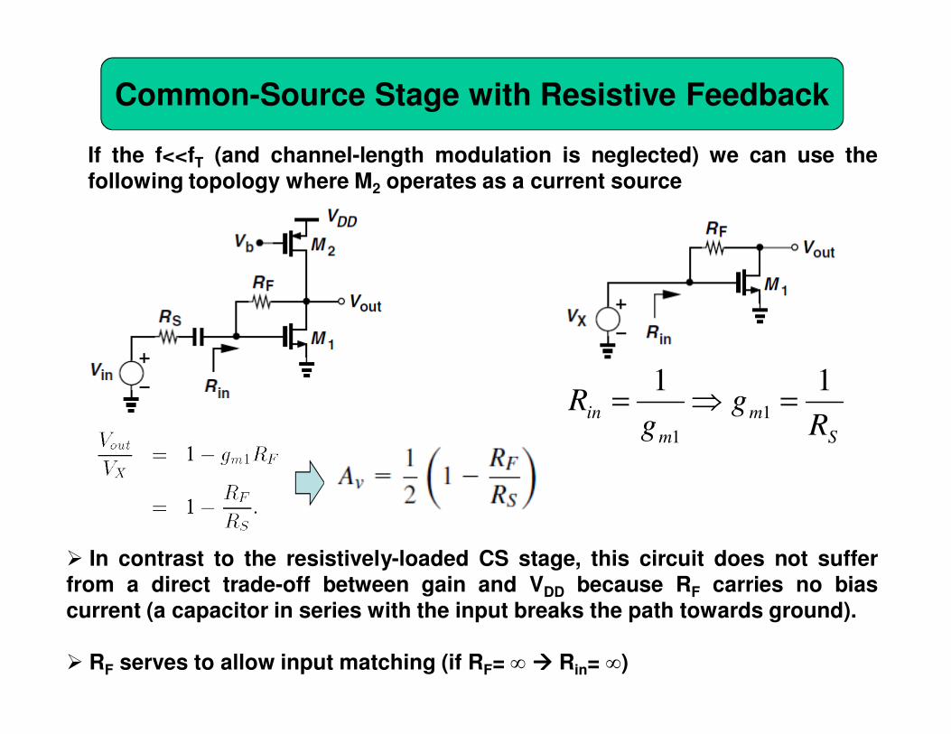
Common-Source Stage with Resistive Feedback
If the f<<fT (and channel-length modulation is neglected) we can use thefollowing topology where M2 operates as a current source
In contrast to the resistively-loaded CS stage, this circuit does not sufferfrom a direct trade-off between gain and VDD because RF carries no biascurrent (a capacitor in series with the input breaks the path towards ground).
RF serves to allow input matching (if RF= ∞ Rin= ∞)
S
m
m
inR
gg
R11
1
1
=⇒=

Noise Figure of CS Stage with Resistive Feedback
The noise of RF appears at the output:
(RF >> RS)
γ γ γ γ ≥ 1 NF ≥ 3 dB
S
mR
g1
1 =
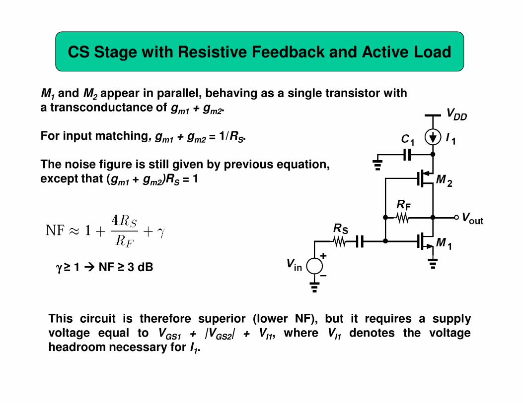
CS Stage with Resistive Feedback and Active Load
M1 and M2 appear in parallel, behaving as a single transistor witha transconductance of gm1 + gm2.
For input matching, gm1 + gm2 = 1/RS.
The noise figure is still given by previous equation,except that (gm1 + gm2)RS = 1
This circuit is therefore superior (lower NF), but it requires a supplyvoltage equal to VGS1 + |VGS2| + VI1, where VI1 denotes the voltageheadroom necessary for I1.
γ γ γ γ ≥ 1 NF ≥ 3 dB

Common-Gate (CG) Stage
The low input impedance of the CG stage makes it attractive for LNA design.Consider only the inductive loading case to avoid the gain-headroom trade-offand neglect r0. At the tank resonance frequency
γ≥ 1 NF > 3 dB
That’s the price for input matching: a higher gm
would increase the gain and reduce NF
min gR /1=
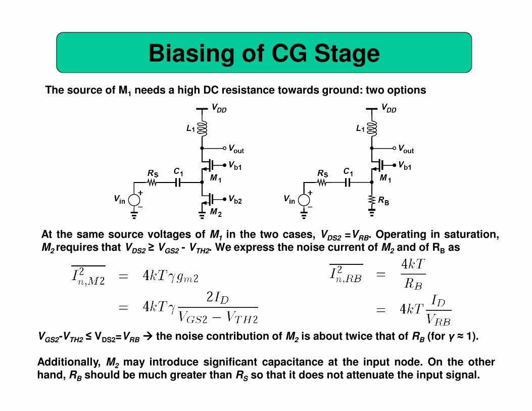
Biasing of CG Stage
At the same source voltages of M1 in the two cases, VDS2 =VRB. Operating in saturation,M2 requires that VDS2 ≥ VGS2 - VTH2. We express the noise current of M2 and of RB as
VGS2-VTH2 ≤ VDS2=VRB the noise contribution of M2 is about twice that of RB (for γ ≈ 1).
Additionally, M2 may introduce significant capacitance at the input node. On the otherhand, RB should be much greater than RS so that it does not attenuate the input signal.
The source of M1 needs a high DC resistance towards ground: two options

Complete example of proper biasing
Biasing of CG Stage
The mirror configuration assures that M1 is in saturation (provided that VDS3>VTH)

Input Impedance of CG Stage in the Presence of rO
the term R1/(gmrO) may become comparable with or even exceed the term1/gm, yielding an input resistance substantially higher than 50 Ω
As technology is scaled down, rO is not negligible.
The positive feedback through rO raises the input impedance.
At the tank resonance frequency
mOmOm
O
X
Xin
grg
R
rg
rR
I
VR
1
1
11 +≈+
+==

Neglecting the capacitances of M1 , at very low or very high frequencies thetank assumes a low impedance, yielding Rin = 1/gm
Input Impedance of CG Stage in the Presence of rO

In order to guarantee input matching:
The voltage gain is
The channel length should be increased in order to raise r0. The devicewidth should be increased proportionally to maintain transconductance
higher gate-source capacitance!
For typical values the gain reduces as r0 reduces. Ex: if rO and R1 are comparable, the voltage gain is on the order of gmrO/4, a very low value.
Input Impedance of CG Stage in the Presence of rO
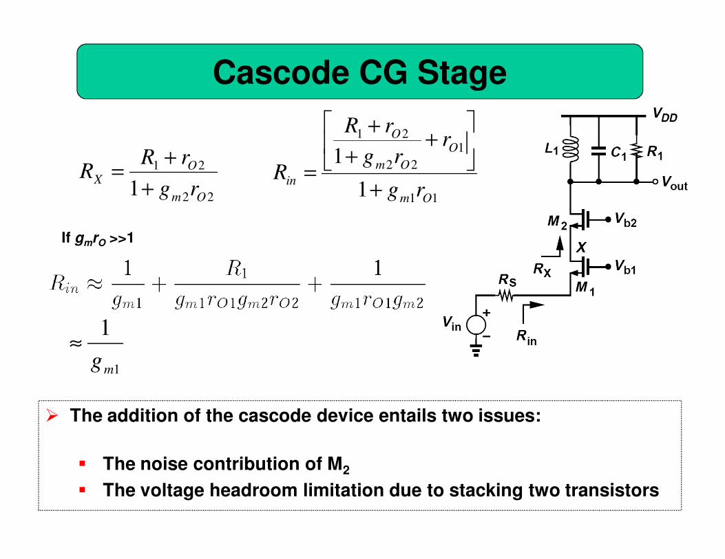
Cascode CG Stage
If gmrO >>1
The addition of the cascode device entails two issues:
The noise contribution of M2
The voltage headroom limitation due to stacking two transistors
11
1
22
21
1
1
Om
O
Om
O
inrg
rrg
rR
R+
+
+
+
=
1
1
mg≈
22
21
1 Om
OX
rg
rRR
+
+=

Issues of Cascode CG Stage: Voltage Headroom Limitation
The two transistors M1 and M2 consume voltage headroom
CG stages often employ an inductor for thebias path
• to avoid the noise-headroom trade-offimposed by RB (the higher is VRB the loweris the resistor noise)
• to cancel the input capacitance of thecircuit (Cpad + CSB1 + CGS1 )
The mirror configuration assuresthat M1 is in saturation (providedthat VDS,B>VTH)

Design Procedure
In the first step, the dimensions and bias current of M1 must be chosen such that a transconductance of (50 Ω)-1 is obtained.
For long channel (square law) transistors
choose L=Lmin =λλλλ to reduce area and gate capacitance
given ID, W1 is calculated by (M1 is in saturation)
S
DnmR
IL
Wkg
12
min
11 ==
The higher is ID, the lower is W: gate-capacitance vs. power consumptiontrade-off
Design Procedure
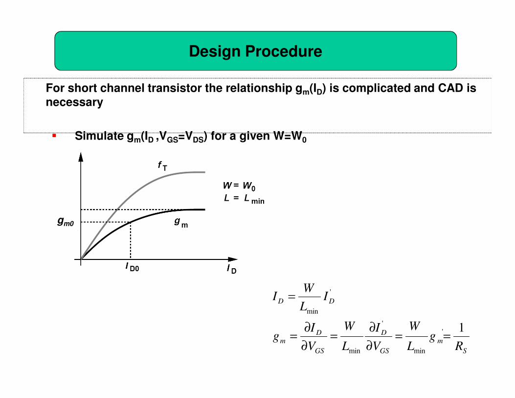
For short channel transistor the relationship gm(ID) is complicated and CAD is necessary
Simulate gm(ID ,VGS=VDS) for a given W=W0
S
m
GS
D
GS
Dm
DD
Rg
L
W
V
I
L
W
V
Ig
IL
WI
1'
min
'
min
'
min
==∂
∂=
∂
∂=
=
gm0

Design Procedure
In the second step, we compute the necessary value of LB
LB must resonate with Cpad + CSB1 + CGS1 and its own capacitance at thefrequency of interest (because LB is unknown some iteration is required)
RP can degrade the NF and can reduce the gain. For example if the totalcapacitance is very high, LB and consequently RP could be low at theresonance frequency so as to reduce the gain.

Design Procedure
In the third step, the bias of M1 is defined by means of MB and IREF
CB must provide a sufficiently lowimpedance (much less than 50ΩΩΩΩ), at theresonance, from the gate of M1 to groundand also bypasses the noise of MB and IREF
to ground.

Design Procedure
Next, the width of M2 must be chosen (L2 is taken at Lmin)
In order to minimize the capacitance at node X, transistors M1 and M2 canbe laid out such that the drain area of the former is shared with the sourcearea of the latter W2=W1.

Design Procedure
In the last step, the value of the load inductor, L1, must be determined
In a manner similar to the choice of LB, we compute L1 such that itresonates with CGD2 + CDB2, the input capacitance of the next stage (C1),and its own capacitance.

LNA Design Example (ⅠⅠⅠⅠ)
Design the LNA for a center frequency of 5.5 GHz in 65-nm CMOS technology. Assume the circuit is designed for an 802.11a receiver.
Figure below plots the transconductance of an NMOS transistor with W = 10 µm and L = 60 nm as a function of the drain current. We select a bias current of 2 mA to achieve a gm of about 10 mS = 1/(100Ω).
Thus, to obtain an input resistance of 50 Ω, we must double the width and drain current. The capacitance introduced by a 20-µm transistor at the input is about 30 fF. To this we add a pad capacitance of 50 fF and choose LB = 10 nH for resonance at 5.5 GHz.

LNA Design Example (ⅡⅡⅡⅡ)
Next, we choose the width of the cascode device equal to 20 µm andassume a load capacitance of 30 fF. This allows the use of a 10-nH inductorfor the load, too, because the total capacitance at the output node amountsto about 75 fF.
The inductor loss is modeledby series and parallelresistances so as to obtain abroadband representation.
However, with a Q ofabout 10 for such aninductor, the LNA gain isexcessively high and itsbandwidth excessivelylow. For this reason, weplace a resistor of 1 kΩ inparallel with the tank.

LNA Design Example (ⅢⅢⅢⅢ)
The simulation results reveal a relatively flat NF and gain from 5 to 6 GHz. The inputreturn loss remains below -18 dB for this range even though we did not refine thechoice of LB (due to its losses).

Cascode CS Stage with Inductive Degeneration: Input Impedance
The feedback through CGD may be exploited to produce the required real part but it also leads to a negative resistance at lower frequencies.
Neglecting CGD
the third term (Rin) can bechosen equal to 50Ω
the degeneration inductor is often realized as abond wire (~ nH) with the reasoning that the latter isinevitable in packaging and must be incorporated inthe design.
Tin
GS
mT LR
C
gωω 1
1
≈⇒≈in 65-nm technology ωT ≈2π(160 GHz) L1 ≈50 pH(very low!)
we can use an explicit capacitor in parallel with CGS to reduce the effective ωωωωT.

Effect of gate-drain capacitance
Assume the drain is tied to a load resistance R1 ≈ 1/gm (as in a cascode)
Assuming that the first two terms in the square brackets are dominant, we
conclude that the input resistance falls by a factor of (1-2CGD/CGS) which is
made positive by increasing the effective CGS as discussed before.

Effect of Pad Capacitance
In addition to CGD, the input pad capacitance of the circuit also lowers the input resistance.
inR
both effect are attenuated if a capacitor is placed in parallel to CGS (lower fT)
fT needs not be reduced so much in order to have R* = 50 Ω.
|ZL1| tipically << |ZCGS|
R*
R*
R*
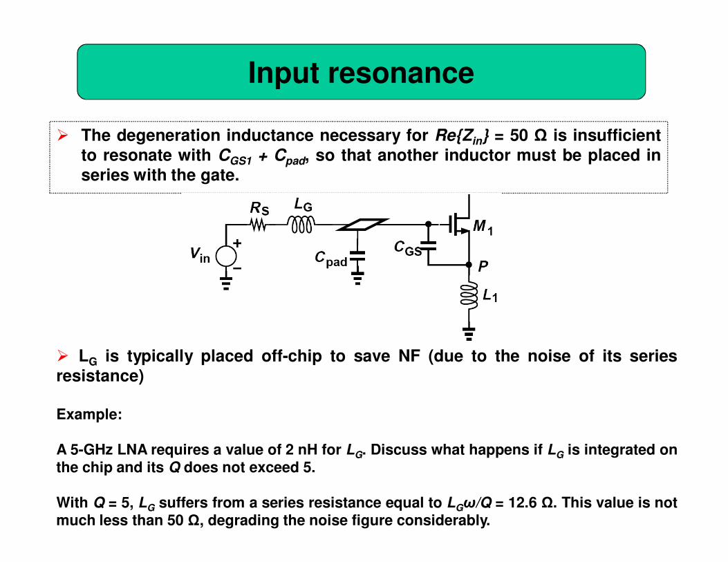
Input resonance
The degeneration inductance necessary for ReZin = 50 Ω is insufficientto resonate with CGS1 + Cpad, so that another inductor must be placed inseries with the gate.
LG is typically placed off-chip to save NF (due to the noise of its seriesresistance)
Example:
A 5-GHz LNA requires a value of 2 nH for LG. Discuss what happens if LG is integrated onthe chip and its Q does not exceed 5.
With Q = 5, LG suffers from a series resistance equal to LGω/Q = 12.6 Ω. This value is notmuch less than 50 Ω, degrading the noise figure considerably.

NF Calculation (ⅠⅠⅠⅠ)
Excluding the effect of channel-length modulation, body effect, CGD and Cpad for simplicity
The coefficient of Iout represents the transconductance gain of the circuit:
At the resonance frequency (ωωωω0) (L1+LG)CGS1ωωωω02+1=0

NF Calculation (ⅡⅡⅡⅡ)
the transconductance of the circuit remains independent of L1, LG, and gm so long asthe input is matched.
For gmL1/CGS1 = RS
the NF at input resonance and input matching:
For input matching gmL1/CGS1=RS

NF Calculation: observations
As the operation frequency is reduced the NF approaches the idealvalues of 0 dB
If the transistor width and bias current are scaled down proportionally,then gm and CGS1 decrease while gm/CGS1 = ωT remains constant the NFdecreases and the power dissipation of the circuit decreases also.
However, as CGS1 decreases, LG + L1 must increase proportionally tomaintain a constant ω0. Increasing L1, the transconductance reduces andcreates input mismatch, so that LG should be increased avoiding largeseries resistances.

Cascode CS Stage with Inductive Degeneration
The voltage gain (at input and output resonance):
The impedance seen at the source of M2,RX rises sharply at the output resonancefrequency.
Including the noise of R1 andneglecting the noise of M2
2
0
1
2
0 41
+
+=
T
S
T
SmR
RRgNF
ω
ω
ω
ωγ
Add a cascode transistor in the output branch to suppress the effect ofnegative resistance (LD- CGD coupling).
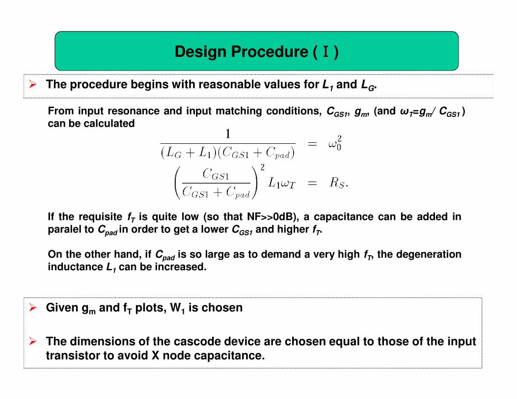
Design Procedure (ⅠⅠⅠⅠ)
The procedure begins with reasonable values for L1 and LG.
From input resonance and input matching conditions, CGS1, gm, (and ωT=gm/ CGS1 )can be calculated
Given gm and fT plots, W1 is chosen
The dimensions of the cascode device are chosen equal to those of the input transistor to avoid X node capacitance.
If the requisite fT is quite low (so that NF>>0dB), a capacitance can be added inparalel to Cpad in order to get a lower CGS1 and higher fT.
On the other hand, if Cpad is so large as to demand a very high fT, the degenerationinductance L1 can be increased.

Design Procedure (ⅡⅡⅡⅡ)
In the last step of the design, we must examine the input match. Due to theMiller multiplication of CGD1 , it is possible that the real and imaginary partsdepart from their ideal values, necessitating some adjustment in LG.
Repeat until desired performances are reached.
A value for LD is selected such that it resonates at ω0 with the drain-bulkand drain-gate capacitances of M2, the input capacitance of the nextstage, and the inductors’s own parasitic capacitance.
If the parallel equivalent resistance of LD results in a gain greater than required, thenan explicit resistor can be placed in parallel with LD to lower the gain and widen thebandwidth.

Alternative Design Procedure
Alternatively, the design procedure can begin with known values for NFand L1 and the following equations:
where the noise of the cascode transistor and the load is neglected.
The necessary values of ωT and gm1 can thus be computed (gm1/CGS1 ≈ ωT).
If the gm, fT (ID) plots indicate that the device fT is too high, then additionalcapacitance can be placed in parallel with CGS1.
Finally, LG is calculated for input resonance by

Final Design of Cascode CS LNA
The antenna is capacitivily tied to the receiver to isolate the LNA bias fromexternal connections.
The bias current of M1 is established by MB and IB, and resistor RB and capacitorCB isolate the signal path from the noise of IB and MB.
Since RB appears in parallel with the signal path, its value must be maximized.However, large resistors may suffer from significant parasitic capacitance.Alternatively, a small MOSFET acting as a resistor can be used here.

Design Example of Cascode CS LNA (ⅠⅠⅠⅠ)
Design a cascode CS LNA for a center frequency of 5.5 GHz in 65-nm CMOS technology.
We begin with a degeneration inductance of 1 nH and the same input transistor as thatin the CG stage in previous example. Interestingly, with a pad capacitance of 50 fF, theinput resistance happens to be around 60Ω. (Without the pad capacitance, ReZin is inthe vicinity of 600 Ω.)We thus simply add enough inductance in series with the gate (LG = 12 nH) to null thereactive component at 5.5 GHz.
The design of the cascode deviceand the output network is identicalto that of the CG example.

Design Example of Cascode CS LNA (ⅡⅡⅡⅡ)
We observe that the CS stage has a higher gain, a lower noise figure, and anarrower bandwidth and higher S11 than the CG stage in previous example.

CG LNA vs. CS LNA
The choice between the CG and CS LNA topologies is determined bythe trade-off between the robustness of the input match and the lowerbound on the noise figure:
the CG LNA provides an accurate input resistance that is relativelyindependent of package parasitics and a much broader band at itsinput
the CS LNA exhibits a higher gain and lower noise figure, but lowerbandwidth
We therefore select the CG stage if the required LNA noise figure canbe around 4 dB, and the CS stage for lower values.

Variants of Common-Gate LNA: CG LNA with
Feedback (ⅠⅠⅠⅠ)
If channel length modulation and body effect are neglected, the closed-loop inputimpedance is equal to:
at resonance
To add a degree of freedom in the design, a block having a gain (orattenuation factor) of α senses the output voltage and subtracts a fractionthereof from the input.
the input resistance can therefore be substantiallyhigher than 1/gm
SR
R
2
1=
if input is matched

Variants of Common-Gate LNA: CG LNA with
Feedback (ⅡⅡⅡⅡ)
Taking into the account also the noise of R1:
The NF can be lowered by raising gm.
This result is identical to that for the simple CG stage, except that gmRS neednot be equal to 1 here
gm can be increased for lower NF while input matching is adjusted by aproper value for αααα
SR=

Design Example of CG LNA with Feedback
The design begins with the choice of gm and R1 to obtain the
required NF and voltage gain Av=R1/2RS (the effective R1 can be
lowered by a parallel resistor to L1).
For input matching
For example, if gmRS=4 and Av=6 (15.6 dB), then R1 = 600ΩΩΩΩ and
α=1/16.
VSm
Sm
ARg
Rg
2
1−=α

CG LNA with Feedforward
Another variant of the CG LNA employs feedforward to avoid the tightrelationship between the input resistance and the noise figure.
( ) inmgsm vAgvg +−= 1
gm is boosted by a factor (1+A)
( ) S
m
in RAg
R =+
=1
1
Rin is reduced by a factor (1+A)
( ) 11 RAgA mv +=
Av (at resonance) is boosted by a factor (1+A)

CG LNA with Feedforward
2/11 nm VRg−=
if input is matched
Taking into the account also the noise of R1 and neglecting the noise of the gain stage A:
the NF can be lowered by raising A with the constrain gm(1+A)=1/RS (for inputmatching).
Taking into the account the noise of the gain stage A:

CG Stage with Transformer Feedforward
In order to minimize the noise of the gain stage A, it is possible to obtain thevoltage gain through the use of an on-chip transformer
On-chip transformer geometries make it difficult to achieve a voltage gain higher than roughly 3

Noise-Canceling LNAs: Basic Ideas
The NF of LNAs is composed of three terms: a value of unity arising from thenoise of RS itself, a term representing the contribution of the input transistor,and another related to the noise of the load resistor. “Noise-cancelling LNAs”aim to cancel the second term.
First identify two nodes at which the signal appears with opposite polarities but the noise of the input transistor appears with the same polarity.
Then their voltages can be properly scaled and summed such that the signal components add and the noise components cancel.

Noise-Canceling LNAs: Noise Figure
choosing A1=1+RF/RS
Taking into account the noise of the gain stage:
Example: CS stage with resistive feedback
(input matched)

Noise-Canceling LNAs: Noise Figure
the noise of M1 is suppressed
NF can be minimized by maximizing RF and minimizing the noise of thegain stage (a higher RF increases the gain also)
the input capacitance, Cin, arising from M1 and the gain stage degradesboth S11 and the noise cancellation, thereby requiring a series (orparallel) inductor at the input for operation at very high frequencies.
It can be proved that the frequency-dependent NF is expressed as(f0=1/ππππRSCin)
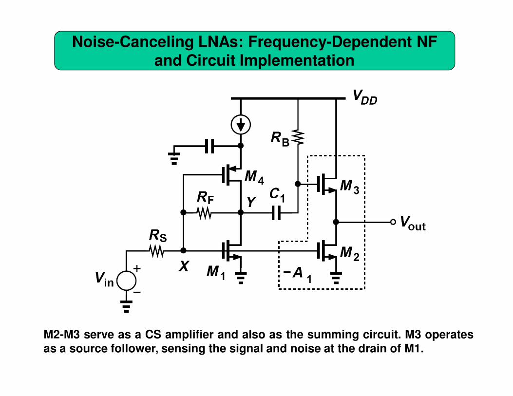
Noise-Canceling LNAs: Frequency-Dependent NF and Circuit Implementation
M2-M3 serve as a CS amplifier and also as the summing circuit. M3 operatesas a source follower, sensing the signal and noise at the drain of M1.

Reactance-Cancelling LNAs
The idea is to exploit the inductive input impedance of a negative-feedbackamplifier so as to cancel the input capacitance, Cin. Assuming a one-pole (ωωωω0)response for the core amplifier
the input admittance is given by
At frequencies well below ω0, 1/ReY1 reduces to RF /(1+A0), which can be set equal to RS, and ImY1 is roughly -A0ω/(RF ω0), which can be chosen to cancel Cinω.

Gain Switching: Effect on NF and P1dB
While designed for the highest sensitivity, the receiver chain muststill detect the signal correctly as the input level continues to increase.
This requires that the gain of each stage be reduced so that thesubsequent stages remain sufficiently linear with the large input signal.
as the gain reduces, the NF rises. The gain must therefore be loweredsuch that the degradation in the sensitivity is less than the increase inthe received signal level, i.e., the SNR does not fall.

Gain Switching: Effect on NF and P1dB
Gain switching in an LNA must deal with several issues:
(1) it must negligibly affect the input matching;
(2) it must provide sufficiently small “gain steps”
(3) the additional devices performing the gain switching must not
degrade the speed of the original LNA;
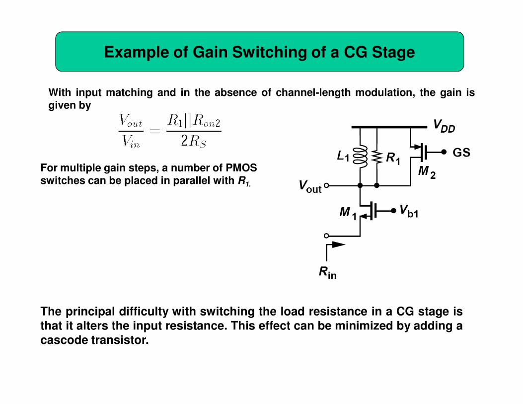
Example of Gain Switching of a CG Stage
With input matching and in the absence of channel-length modulation, the gain isgiven by
For multiple gain steps, a number of PMOS switches can be placed in parallel with R1.
The principal difficulty with switching the load resistance in a CG stage isthat it alters the input resistance. This effect can be minimized by adding acascode transistor.

Example of the Load Switching Network Design
Design the load switching network of figure above for two 3-dB gain steps.
As shown in figure below, M2a and M2b switch the gain. For the first 3-dB reduction in gain, M2a is turned on and
Solution:
For the second 3-dB reduction, both M2a
and M2b are turned on and

Band Switching
LNAs that must operate across a wide bandwidth or in different bands, can incorporate band switching
when S1 is ON, the total capacitance becomes C1+C2 lowering the resonance frequency

Even-Order Distortion
Asymmetries in the mixer or in the LO waveform allow a fraction of the RF input ofthe mixer to appear at the output without frequency translation, corrupting thedownconverted signal.
Since the feedthrough of the beat depends on the mixer and LO asymmetries, thebeat amplitude measured in the baseband depends on the device dimensions and thelayout and is therefore difficult to formulate.
Direct-conversion receivers are additionally sensitive to even-ordernonlinearity in the RF path.

Second Intercept Point (IP2)
If Vin(t) = Acos ω1t + Acos ω2t, then the LNA output is given by
Beat amplitude grows with the square of the amplitude of the input tones.

Example of Calculation of IP2
Solution:
Suppose the attenuation factor experienced by the beat as it travels through the mixer is equal to k whereas the gain seen by each tone as it is downconverted to the baseband is equal to unity. Calculate the IP2.
From equation above, the value of A that makes the output beat amplitude, kα2A2,
equal to the main tone amplitude, α1A, is given by

High-IP2 LNAs: Differential LNAs
Since the circuits following the downconversion mixers are typically realized indifferential form, they exhibit a high IP2, leaving the LNA and the mixers as theIP2 bottleneck of the receivers.
Differential LNAs can achieve high IP2’s because, symmetric circuits produceno even-order distortion. Example: CG (left) and CS (right)
In principle, any of the single-ended LNAs studied thus far can be converted to differential form.

Use of Balun at RX Input
Since the antenna and the preselect filter are typically single-ended, atransformer must precede the LNA to perform single-ended to differentialconversion.
The transformer is called a “balun,” an acronym for “balanced-to-unbalanced” conversion because it can also perform differential to single-ended conversion if its two ports are swapped.
For a lossless 1-to-1 balun, we have RS2=RS1.
The differential input impedance of the LNA, Rin, must be equal to RS1 forproper input matching the single-ended input impedance of each halfcircuit must be equal to RS1/2=25ΩΩΩΩ.

Differential CG LNA
Assuming it is designed such that the impedance seen between each input node and ground is equal to RS1/2
• Substitute in the half circuit RS with RS1/2
• gm of each stage is doubled: gm=1/(RS1/2)
• The gain of the half circuit is doubled : VY/VX=R1/(2RS1/2)=R1/RS1

Comparison of Single-Ended and Differential CG LNAs
• The overal gain (VY-VW)/(VX-VZ) = VY/VX is doubled wrt to single-ended stage (the two LNA inputs are +vin/2 and –vin/2 wrt ground).

Differential CG LNA
Differential CG LNA Single-ended CG LNA
The differential configuration exihibits a lower NF due to the higher gain.
The value of R1 can be halved in order to have the same gain and NF of the single-end configutation.
For a given NF, a differentil CG LNA consumes 4 times the power of a single-endedstage (two stages and double current for the double gm)
From the symmetry of the circuit that we can compute the output noise of eachhalf circuit and add the output powers:

Example of Differential Version and Noise Figure
An amplifier having a high input impedance employs a parallel resistor at the input to provide matching. Determine the noise figure of the circuit and its diff. version, shown below (middle), where two replicas of the amplifier are used.
Noise figure of the single-ended circuit: For the differential version:
In this case, the NF of the diff. circuit is higher whether the differential version ofan LNA exhibits a higher or lower NF depends on the circuit topology.

Differential CS LNA
Recall that the input resistance of each half circuit is equal to L1ωT andmust now be halved. This is accomplished by halving L1.
With input matching and a degeneration inductance of L1, the voltage gainwas found to be R1/(2L1ω0), which is now doubled.

Differential CS LNA: Noise Figure
Neglecting the contribution of the cascode device, if the input is matched, half of thenoise current of the input transistor flows from the output node.
14
2
0
1
2
0 +
+
=
T
S
T
SmR
RRgNF
ω
ω
ω
ωγ
Differential CG LNA
Single-ended CG LNA
Compared with the NF of the original Single-Ended LNA, both thetransistor contribution and the load contribution are halved.
This result holds only if the design can employ 2 degeneration inductors,each having half the value of that in the single-ended counterpart (this isdifficult with bond wires as their physical length cannot be shortenedarbitrarily).

Differential CS Stage with On-Chip Degeneration Inductors
The effect of the bond wire is null if the circuit has perfect simmetry
on-chip inductors suffer from low quality factor (high series resistance)
The NF advantage implied previously may not materialize in reality becausethe loss of the balun is not negligible.
Alternatively, the design can incorporate on-chip degeneration inductorswhile converting the effect of the (inevitable) bond wire to a common-modeinductance.

Singe-Ended Antenna Signal to Differential Conversion by Differential Pair
At low to moderate frequencies,VX and VY are differential and thevoltage gain is equal to gm1,2RD.
At high frequencies, however,two effects degrade the balanceof the phases: the parasiticcapacitance at node P and thegate-drain capacitance of M1
(providing a non-invertingfeedforward path around M1)
The capacitance at P can be nulledthrough the use of a parallelinductor, but the CGD1 feedforwardpersists.

Use of On-Chip Inductors for Resonance and Degeneration
The topology discussed above still does not provide input matching. Wemust therefore insert (on-chip) inductances in series with the sources ofM1 and M2.
Here, LP1 and LP2 resonate with CP1 and CP2, respectively, and LS1+LS2
provides the necessary input resistance (LS1+LS2 is realized as oneinductor).
However, this topology exhibits a low IP3

Balun Issues
External baluns with a low loss (e.g., 0.5 dB) in the gigahertz range are available from manufacturers, but they consume board space and raise the cost.
Integrated baluns, on the other hand, suffer from a relatively high loss and large capacitances.
The resistance and capacitance associated with the spirals and the sub-unity coupling factor make such baluns less attractive.
1:1 balun

Use of 1-to-N Balun in an LNA
A student attempts to use a 1-to-N balun with a differential CS stage so as to amplify the input voltage by a factor of N and potentially achieve a lower noise figure. Compute the noise figure in this case.
Since still half of the noise current of each input transistor flows to the output node, the noise power measured at each output is given by
The gain from Vin to the differential output is now equal to NR1/(2L1ω0). Doubling the above power, dividing by the square of the gain, and normalizing to 4kTRS, we have
We note that the first two termshave risen by a factor of N2 !!!

Realization of Baluns with Non-Unity Turns Ratio
a N-to-1 (rather than 1-to-N) balun would be beneficial multiplying the firsttwo terms by 1/N2 rather than N2.
on-chip baluns with a non-unity turns ratio are difficult to design andsuffer from a higher loss and a lower coupling factor.
Stacked Spirals

Other Methods of IP2 Improvement
The difficulty with the use of off-chip oron-chip baluns at the input of differentialLNAs makes single-ended topologies stillan attractive choice.
A possible approach to raising the IP2
entails simply high-pass filtering the low-frequency second-order intermodulationproduct (beat component).
Example: two interferers are located at the edges of the 2.4-GHz band, f1=2.4 GHz,f2=2.480 GHz. The beat therefore lies at 80MHz and is attenuated by approximately afactor of 2400/80=30 for a first-order HPF.
With this substantial suppression, the IP2 of the LNA is unlikely to limit the RXperformance, calling for techniques that improve the IP2 of mixers.
The filtration of the IM2 product becomes less effective for wider communicationbands. For example, if a receiver must accommodate frequencies from 1 GHz to 10GHz, then two interferers can produce a beat within the band, prohibiting the use offilters to remove the beat. In this case, the LNA may become the receiver’s IP2bottleneck.