Embed Size (px)
Citation preview
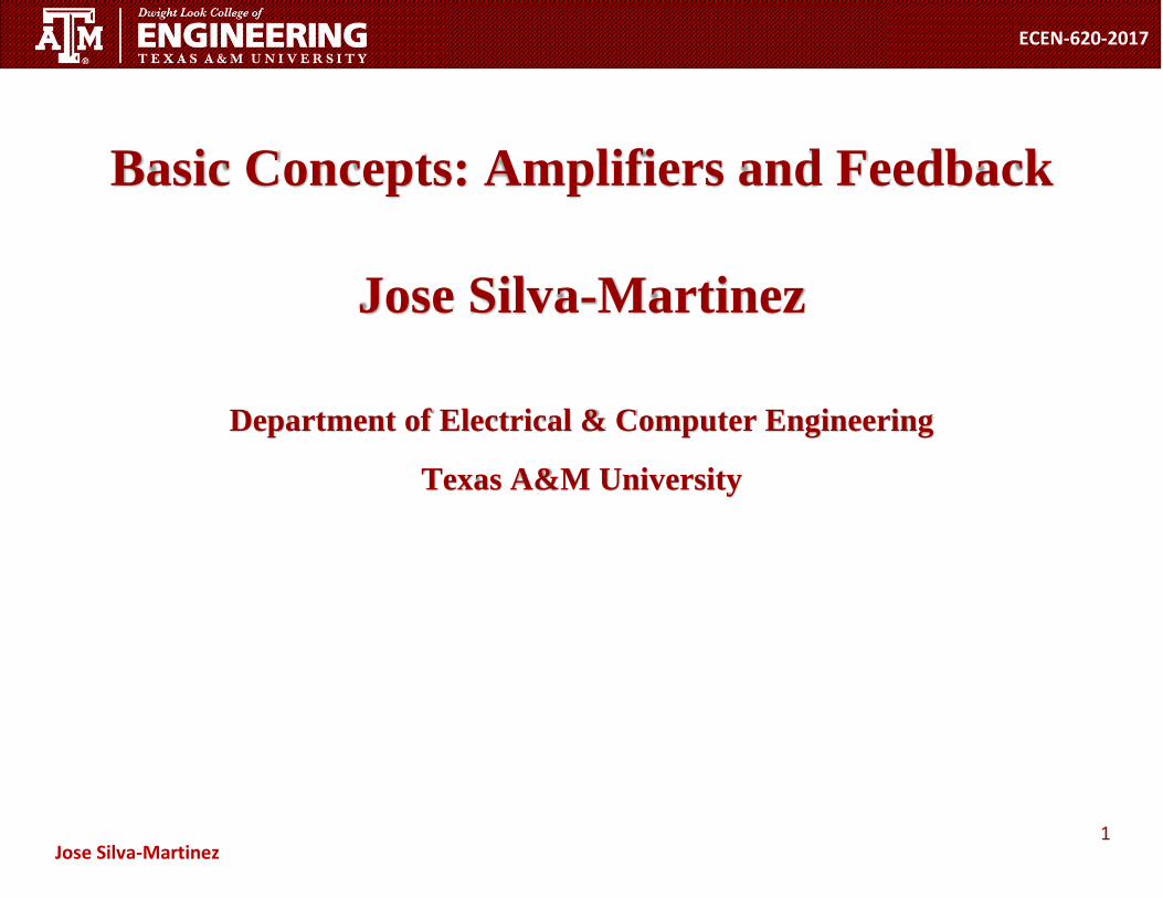
1
ECEN-620-2017
Jose Silva-Martinez
Basic Concepts: Amplifiers and Feedback
Jose Silva-Martinez
Department of Electrical & Computer Engineering
Texas A&M University
2
ECEN-620-2017
Jose Silva-Martinez
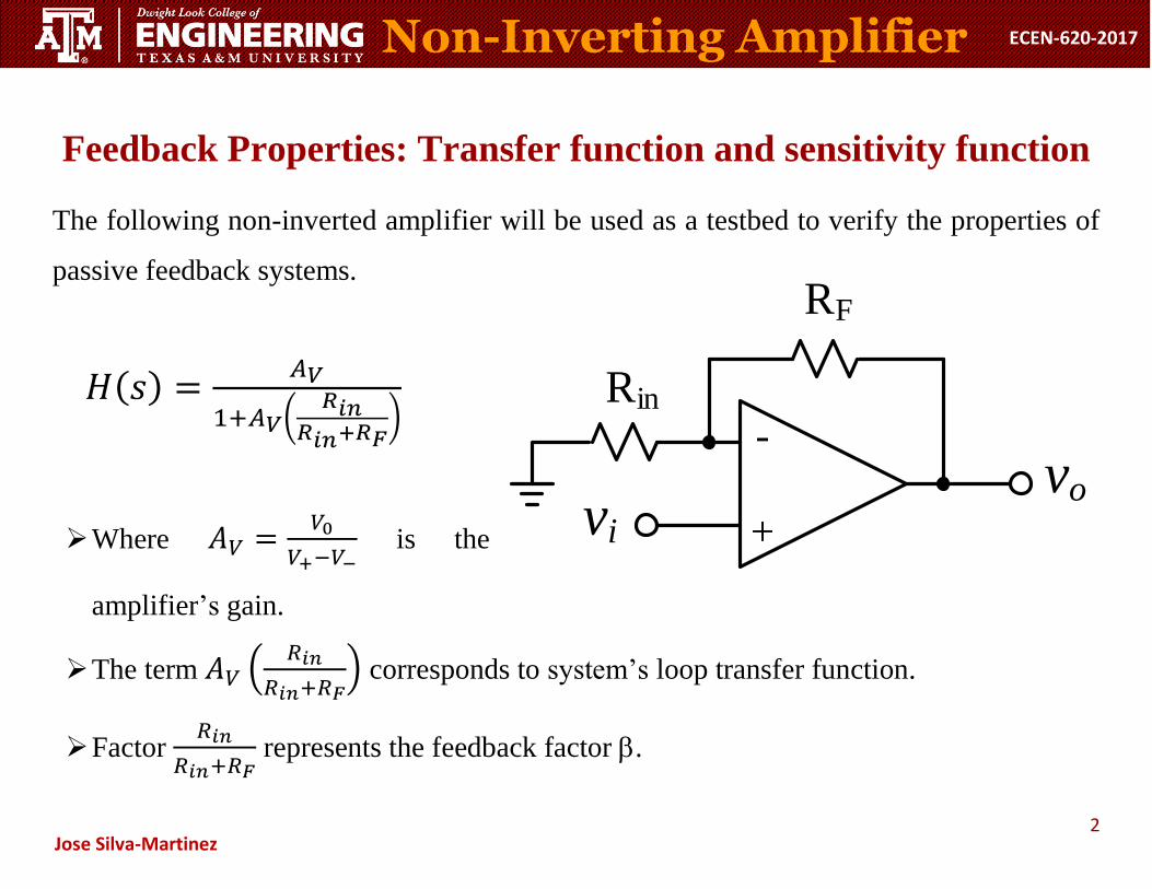
Feedback Properties: Transfer function and sensitivity function
The following non-inverted amplifier will be used as a testbed to verify the properties of
passive feedback systems.
𝐻(𝑠) =𝐴𝑉
1+𝐴𝑉(𝑅𝑖𝑛
𝑅𝑖𝑛+𝑅𝐹)
Where 𝐴𝑉 =𝑉0
𝑉+−𝑉− is the
amplifier’s gain.
The term 𝐴𝑉 (𝑅𝑖𝑛
𝑅𝑖𝑛+𝑅𝐹) corresponds to system’s loop transfer function.
Factor 𝑅𝑖𝑛
𝑅𝑖𝑛+𝑅𝐹 represents the feedback factor .
vi
+
-vo
RF
Rin
Non-Inverting Amplifier
3
ECEN-620-2017
Jose Silva-Martinez
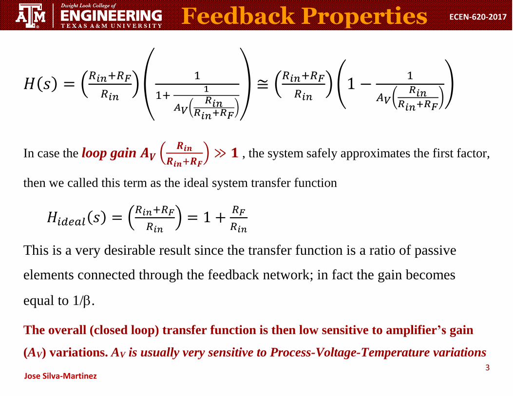
𝐻(𝑠) = (𝑅𝑖𝑛+𝑅𝐹
𝑅𝑖𝑛)(
1
1+ 1
𝐴𝑉(𝑅𝑖𝑛
𝑅𝑖𝑛+𝑅𝐹)
) ≅ (𝑅𝑖𝑛+𝑅𝐹
𝑅𝑖𝑛)(1 −
1
𝐴𝑉(𝑅𝑖𝑛
𝑅𝑖𝑛+𝑅𝐹))
In case the loop gain 𝑨𝑽 (𝑹𝒊𝒏
𝑹𝒊𝒏+𝑹𝑭) ≫ 𝟏 , the system safely approximates the first factor,
then we called this term as the ideal system transfer function
𝐻𝑖𝑑𝑒𝑎𝑙(𝑠) = (𝑅𝑖𝑛+𝑅𝐹
𝑅𝑖𝑛) = 1 +
𝑅𝐹
𝑅𝑖𝑛
This is a very desirable result since the transfer function is a ratio of passive
elements connected through the feedback network; in fact the gain becomes
equal to 1/.
The overall (closed loop) transfer function is then low sensitive to amplifier’s gain
(AV) variations. AV is usually very sensitive to Process-Voltage-Temperature variations
Feedback Properties
4
ECEN-620-2017
Jose Silva-Martinez
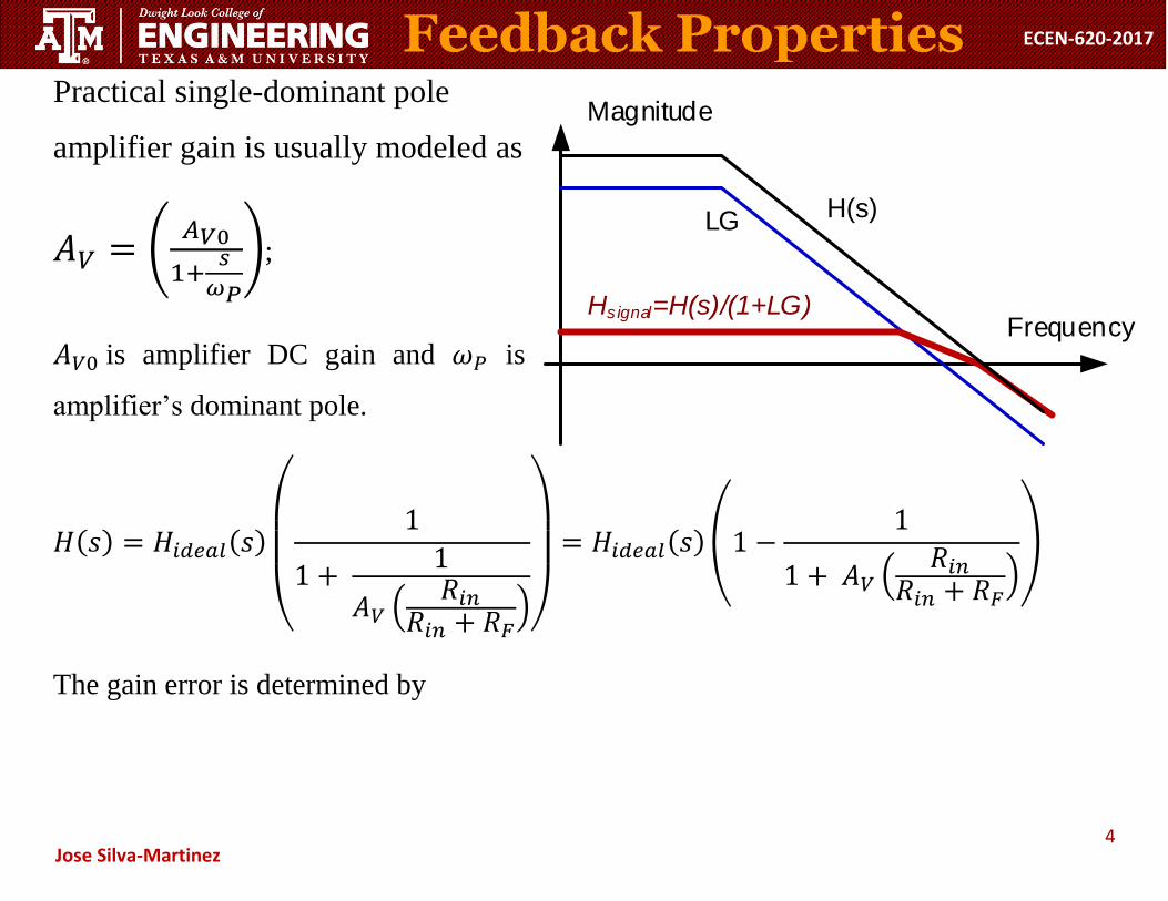
Practical single-dominant pole
amplifier gain is usually modeled as
𝐴𝑉 = (𝐴𝑉0
1+𝑠
𝜔𝑃
);
𝐴𝑉0 is amplifier DC gain and 𝜔𝑃 is
amplifier’s dominant pole.
𝐻(𝑠) = 𝐻𝑖𝑑𝑒𝑎𝑙(𝑠)
(
1
1 + 1
𝐴𝑉 (𝑅𝑖𝑛
𝑅𝑖𝑛 + 𝑅𝐹))
= 𝐻𝑖𝑑𝑒𝑎𝑙(𝑠)(1 −
1
1 + 𝐴𝑉 (𝑅𝑖𝑛
𝑅𝑖𝑛 + 𝑅𝐹))
The gain error is determined by
Feedback Properties
LG
Hsignal=H(s)/(1+LG)
Magnitude
Frequency
H(s)
5
ECEN-620-2017
Jose Silva-Martinez
in
Fin
V
P
R
RR
A
s
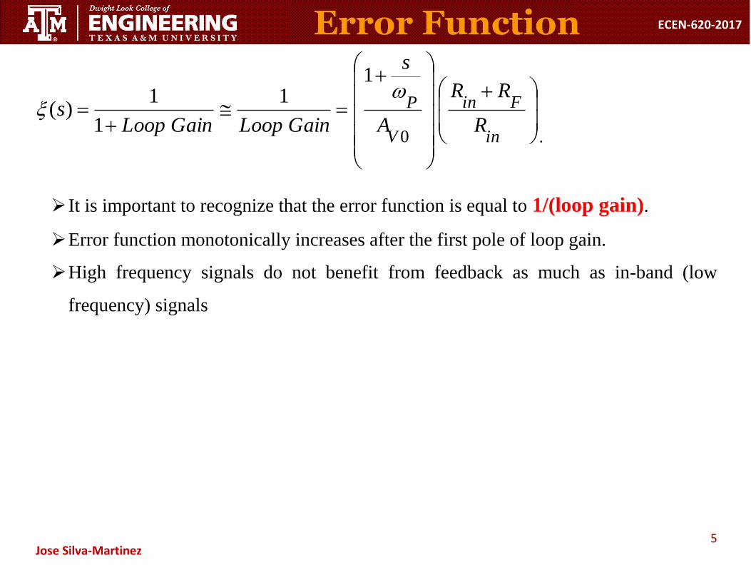
GainLoopGainLoops
0
11
1
1)(
.
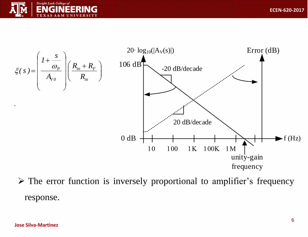
It is important to recognize that the error function is equal to 1/(loop gain).
Error function monotonically increases after the first pole of loop gain.
High frequency signals do not benefit from feedback as much as in-band (low
frequency) signals
Error Function
6
ECEN-620-2017
Jose Silva-Martinez
in
Fin
0V
P
R
RR
A
s1
)s(
.
The error function is inversely proportional to amplifier’s frequency
response.
f (Hz)
20 log10(|AV(s)|)
-20 dB/decade
106 dB
unity-gain
frequency
0 dB
20 dB/decade
Error (dB)
7
ECEN-620-2017
Jose Silva-Martinez
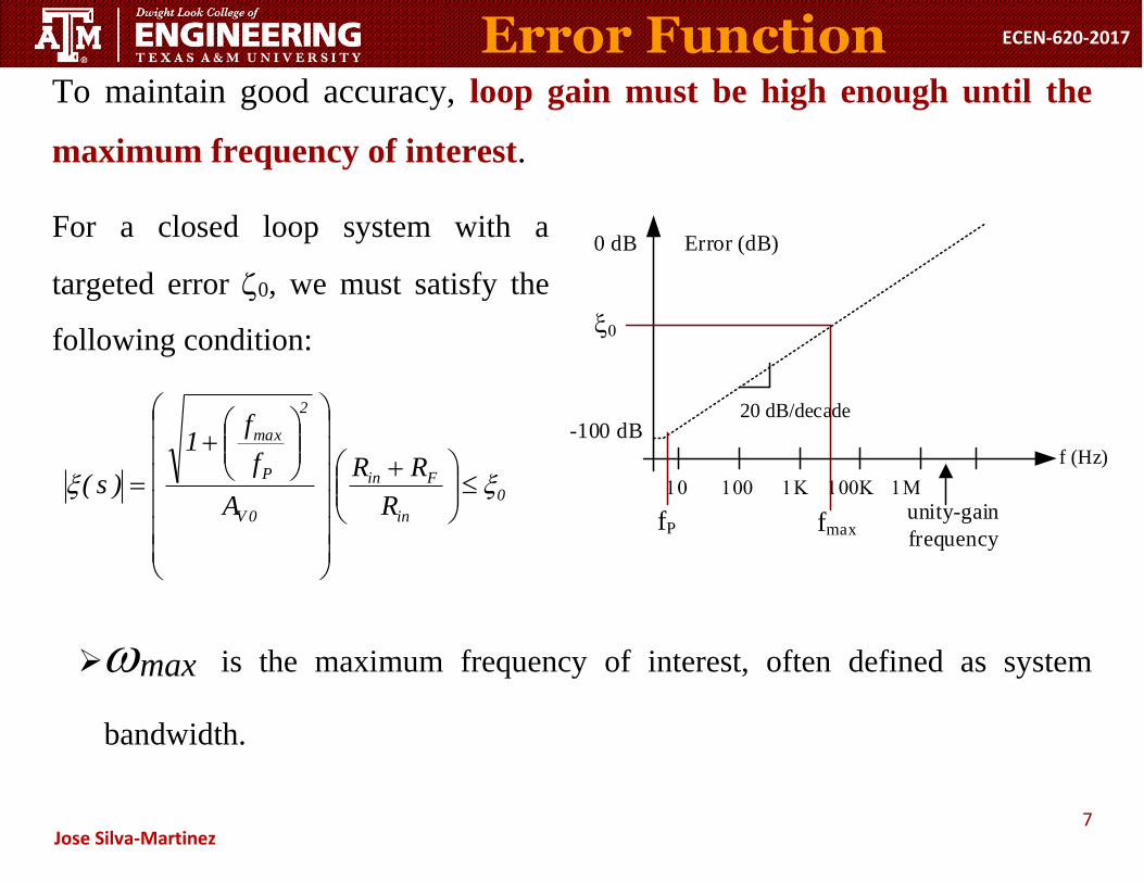
To maintain good accuracy, loop gain must be high enough until the
maximum frequency of interest.
For a closed loop system with a
targeted error 0, we must satisfy the
following condition:
0
in
Fin
0V
2
P
max
R
RR
A
f
f1
)s(
max is the maximum frequency of interest, often defined as system
bandwidth.
f (Hz)
0 dB
unity-gain
frequency
20 dB/decade
Error (dB)
-100 dB
fmax fP
Error Function
8
ECEN-620-2017
Jose Silva-Martinez
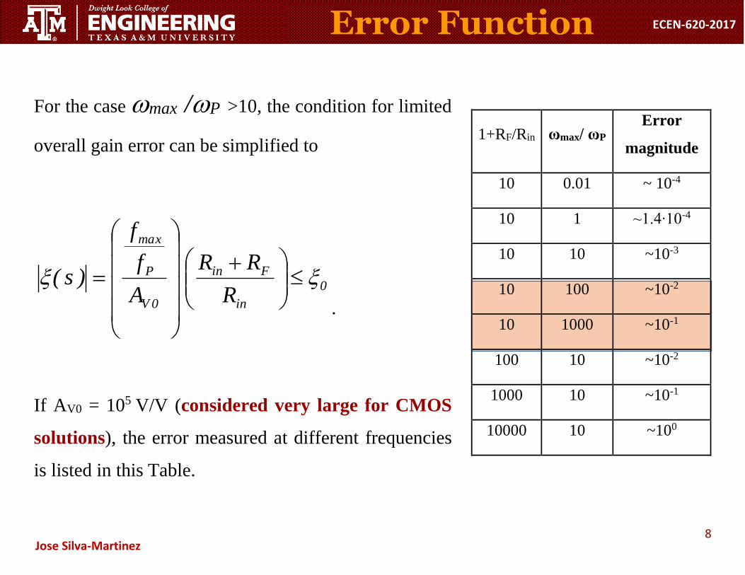
For the case max /P >10, the condition for limited
overall gain error can be simplified to
0
in
Fin
0V
P
max
R
RR
A
f
f
)s(
.
If AV0 = 105 V/V (considered very large for CMOS
solutions), the error measured at different frequencies
is listed in this Table.
1+RF/Rin ωmax/ ωP Error
magnitude
10 0.01 ~ 10-4
10 1 ~1.4∙10-4
10 10 ~10-3
10 100 ~10-2
10 1000 ~10-1
100 10 ~10-2
1000 10 ~10-1
10000 10 ~100
Error Function
9
ECEN-620-2017
Jose Silva-Martinez
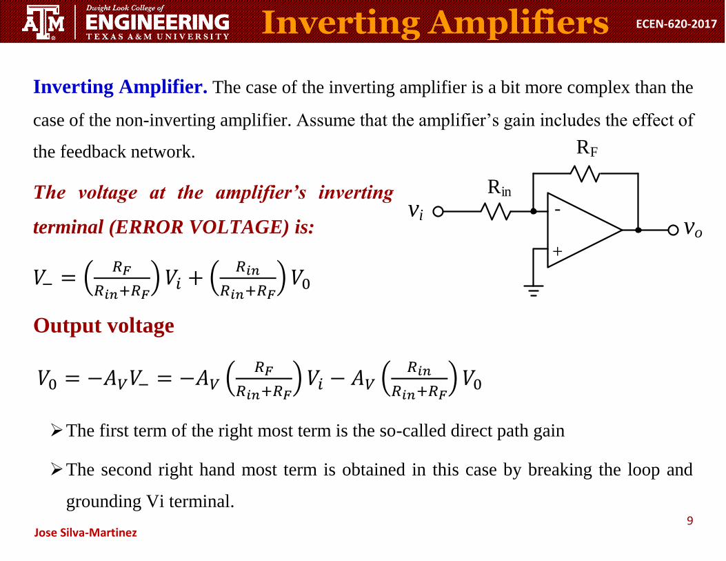
Inverting Amplifier. The case of the inverting amplifier is a bit more complex than the
case of the non-inverting amplifier. Assume that the amplifier’s gain includes the effect of
the feedback network.
The voltage at the amplifier’s inverting
terminal (ERROR VOLTAGE) is:
𝑉− = (𝑅𝐹
𝑅𝑖𝑛+𝑅𝐹)𝑉𝑖 + (
𝑅𝑖𝑛
𝑅𝑖𝑛+𝑅𝐹)𝑉0
Output voltage
𝑉0 = −𝐴𝑉𝑉− = −𝐴𝑉 (𝑅𝐹
𝑅𝑖𝑛+𝑅𝐹)𝑉𝑖 − 𝐴𝑉 (
𝑅𝑖𝑛
𝑅𝑖𝑛+𝑅𝐹)𝑉0
The first term of the right most term is the so-called direct path gain
The second right hand most term is obtained in this case by breaking the loop and
grounding Vi terminal.
+
-
vo
RF
Rin
vi
Inverting Amplifiers
10
ECEN-620-2017
Jose Silva-Martinez
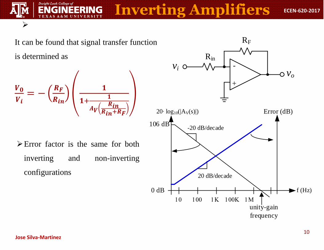
It can be found that signal transfer function
is determined as
𝑽𝟎
𝑽𝒊= −(
𝑹𝑭
𝑹𝒊𝒏)(
𝟏
𝟏+𝟏
𝑨𝑽(𝑹𝒊𝒏
𝑹𝒊𝒏+𝑹𝑭)
)
Error factor is the same for both
inverting and non-inverting
configurations
+
-
vo
RF
Rin
vi
f (Hz)
20 log10(|AV(s)|)
-20 dB/decade
106 dB
unity-gain
frequency
0 dB
20 dB/decade
Error (dB)
Inverting Amplifiers
11
ECEN-620-2017
Jose Silva-Martinez
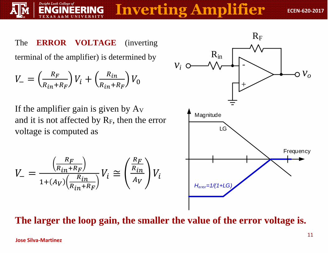
The ERROR VOLTAGE (inverting
terminal of the amplifier) is determined by
𝑉− = (𝑅𝐹
𝑅𝑖𝑛+𝑅𝐹)𝑉𝑖 + (
𝑅𝑖𝑛
𝑅𝑖𝑛+𝑅𝐹)𝑉0
If the amplifier gain is given by AV
and it is not affected by RF, then the error
voltage is computed as
𝑉− =(
𝑅𝐹𝑅𝑖𝑛+𝑅𝐹
)
1+(𝐴𝑉)(𝑅𝑖𝑛
𝑅𝑖𝑛+𝑅𝐹)𝑉𝑖 ≅ (
𝑅𝐹𝑅𝑖𝑛
𝐴𝑉)𝑉𝑖
The larger the loop gain, the smaller the value of the error voltage is.
+
-
vo
RF
Rin
vi
Inverting Amplifier
LG
Herror=1/(1+LG)
Magnitude
Frequency
12
ECEN-620-2017
Jose Silva-Martinez
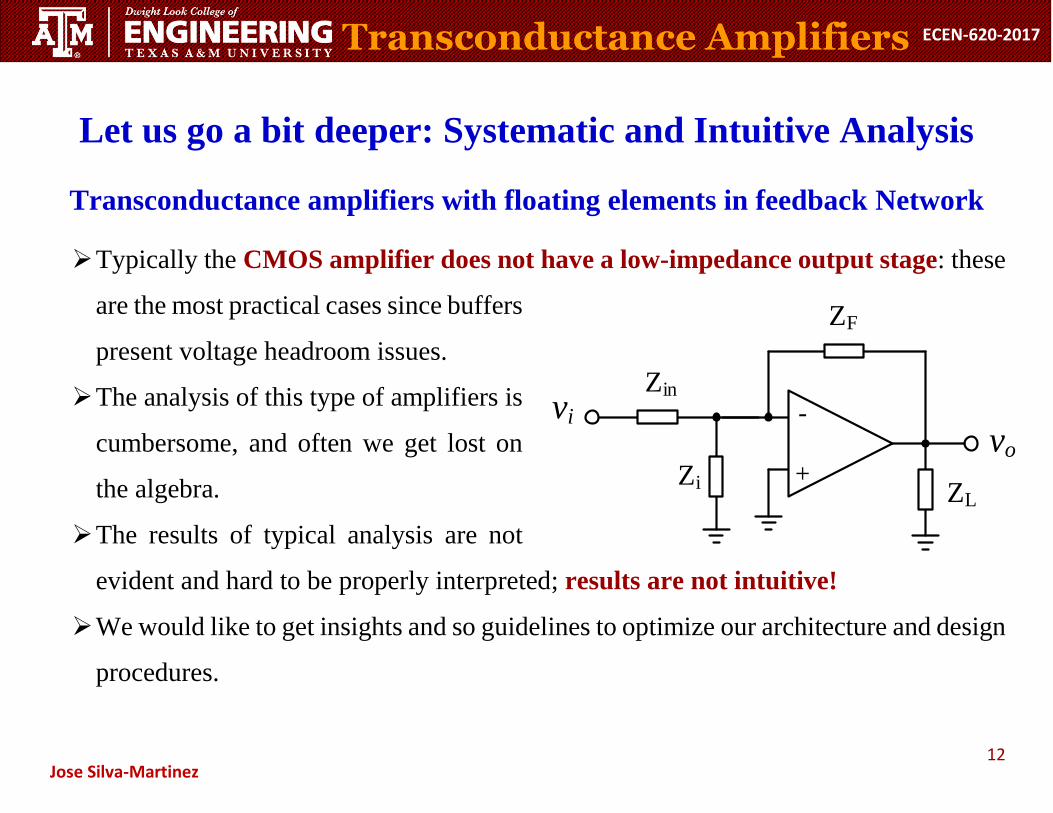
Let us go a bit deeper: Systematic and Intuitive Analysis
Transconductance amplifiers with floating elements in feedback Network
Typically the CMOS amplifier does not have a low-impedance output stage: these
are the most practical cases since buffers
present voltage headroom issues.
The analysis of this type of amplifiers is
cumbersome, and often we get lost on
the algebra.
The results of typical analysis are not
evident and hard to be properly interpreted; results are not intuitive!
We would like to get insights and so guidelines to optimize our architecture and design
procedures.
vi
vo
Zin
Zi
ZF
ZL
+
-
Transconductance Amplifiers
13
ECEN-620-2017
Jose Silva-Martinez
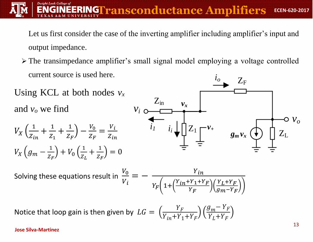
Let us first consider the case of the inverting amplifier including amplifier’s input and
output impedance.
The transimpedance amplifier’s small signal model employing a voltage controlled
current source is used here.
Using KCL at both nodes vx
and vo we find
𝑉𝑋 (1
𝑍𝑖𝑛+
1
𝑍1+
1
𝑍𝐹) −
𝑉0
𝑍𝐹=
𝑉𝑖
𝑍𝑖𝑛
𝑉𝑋 (𝑔𝑚 −1
𝑍𝐹) + 𝑉0 (
1
𝑍𝐿+
1
𝑍𝐹) = 0
Solving these equations result in 𝑉0
𝑉𝑖= −
𝑌𝑖𝑛
𝑌𝐹(1+(𝑌𝑖𝑛+𝑌1+𝑌𝐹
𝑌𝐹)(𝑌𝐿+𝑌𝐹𝑔𝑚−𝑌𝐹
))
Notice that loop gain is then given by 𝐿𝐺 = (𝑌𝐹
𝑌𝑖𝑛+𝑌1+𝑌𝐹) (𝑔𝑚− 𝑌𝐹𝑌𝐿+𝑌𝐹
)
vi
vo
Zin
Z1
ZF
vx
i1 ii
io
ZLgm vx
v+
Transconductance Amplifiers
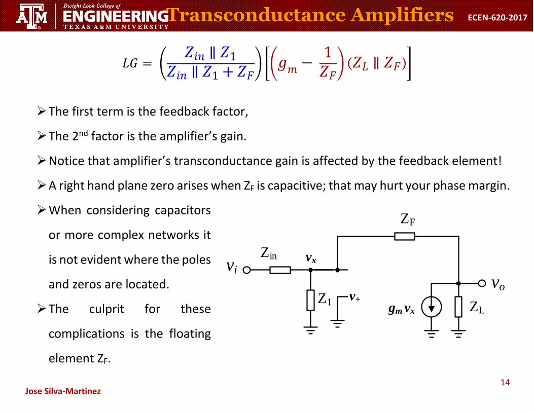
14
ECEN-620-2017
Jose Silva-Martinez
𝐿𝐺 = (𝑍𝑖𝑛 ∥ 𝑍1
𝑍𝑖𝑛 ∥ 𝑍1+𝑍𝐹) [(𝑔𝑚−
1𝑍𝐹) (𝑍𝐿 ∥ 𝑍𝐹)]
The first term is the feedback factor,
The 2nd factor is the amplifier’s gain.
Notice that amplifier’s transconductance gain is affected by the feedback element!
A right hand plane zero arises when ZF is capacitive; that may hurt your phase margin.
When considering capacitors
or more complex networks it
is not evident where the poles
and zeros are located.
The culprit for these
complications is the floating
element ZF.
vi
vo
Zin
Z1
ZF
vx
ZLgm vx
v+
Transconductance Amplifiers
15
ECEN-620-2017
Jose Silva-Martinez
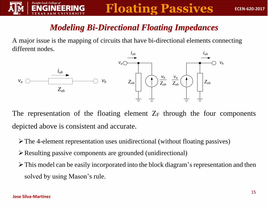
Modeling Bi-Directional Floating Impedances
A major issue is the mapping of circuits that have bi-directional elements connecting
different nodes.
The representation of the floating element ZF through the four components
depicted above is consistent and accurate.
The 4-element representation uses unidirectional (without floating passives)
Resulting passive components are grounded (unidirectional)
This model can be easily incorporated into the block diagram’s representation and then
solved by using Mason’s rule.
va vb
iab
Zab Zab
vb
iab
ZabZab
vava vb
iab
Zab
Floating Passives
16
ECEN-620-2017
Jose Silva-Martinez
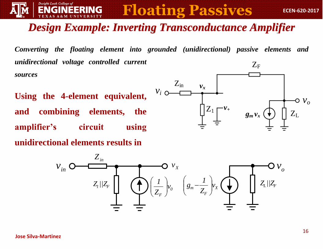
Design Example: Inverting Transconductance Amplifier
Converting the floating element into grounded (unidirectional) passive elements and
unidirectional voltage controlled current
sources
Using the 4-element equivalent,
and combining elements, the
amplifier’s circuit using
unidirectional elements results in
vi
vo
Zin
Z1
ZF
vx
ZLgm vx
v+
X
F
m vZ
1g
FL Z||Z
0
F
vZ
1
F1 Z||Z
inv ovinZ
Xv
Floating Passives
17
ECEN-620-2017
Jose Silva-Martinez
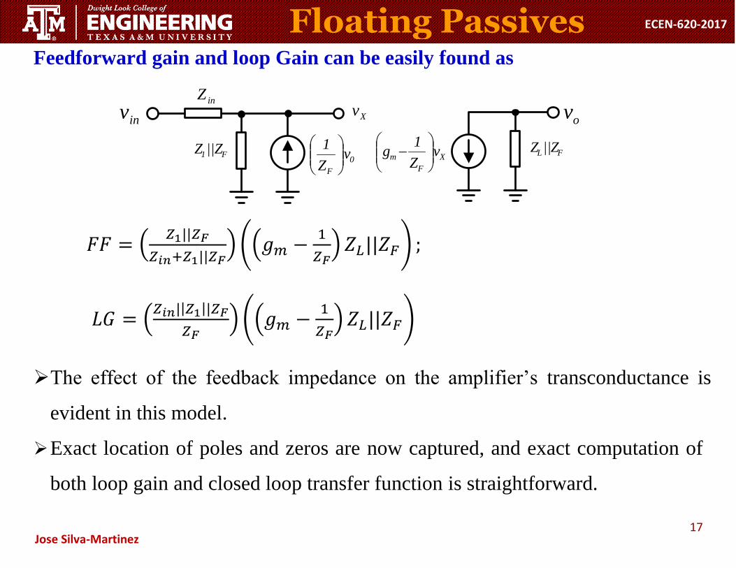
Feedforward gain and loop Gain can be easily found as
𝐹𝐹 = (𝑍1||𝑍𝐹
𝑍𝑖𝑛+𝑍1||𝑍𝐹) ((𝑔𝑚 −
1
𝑍𝐹) 𝑍𝐿||𝑍𝐹) ;
𝐿𝐺 = (𝑍𝑖𝑛||𝑍1||𝑍𝐹
𝑍𝐹) ((𝑔𝑚 −
1
𝑍𝐹) 𝑍𝐿||𝑍𝐹)
The effect of the feedback impedance on the amplifier’s transconductance is
evident in this model.
Exact location of poles and zeros are now captured, and exact computation of
both loop gain and closed loop transfer function is straightforward.
X
F
m vZ
1g
FL Z||Z
0
F
vZ
1
F1 Z||Z
inv ovinZ
Xv
Floating Passives
18
ECEN-620-2017
Jose Silva-Martinez
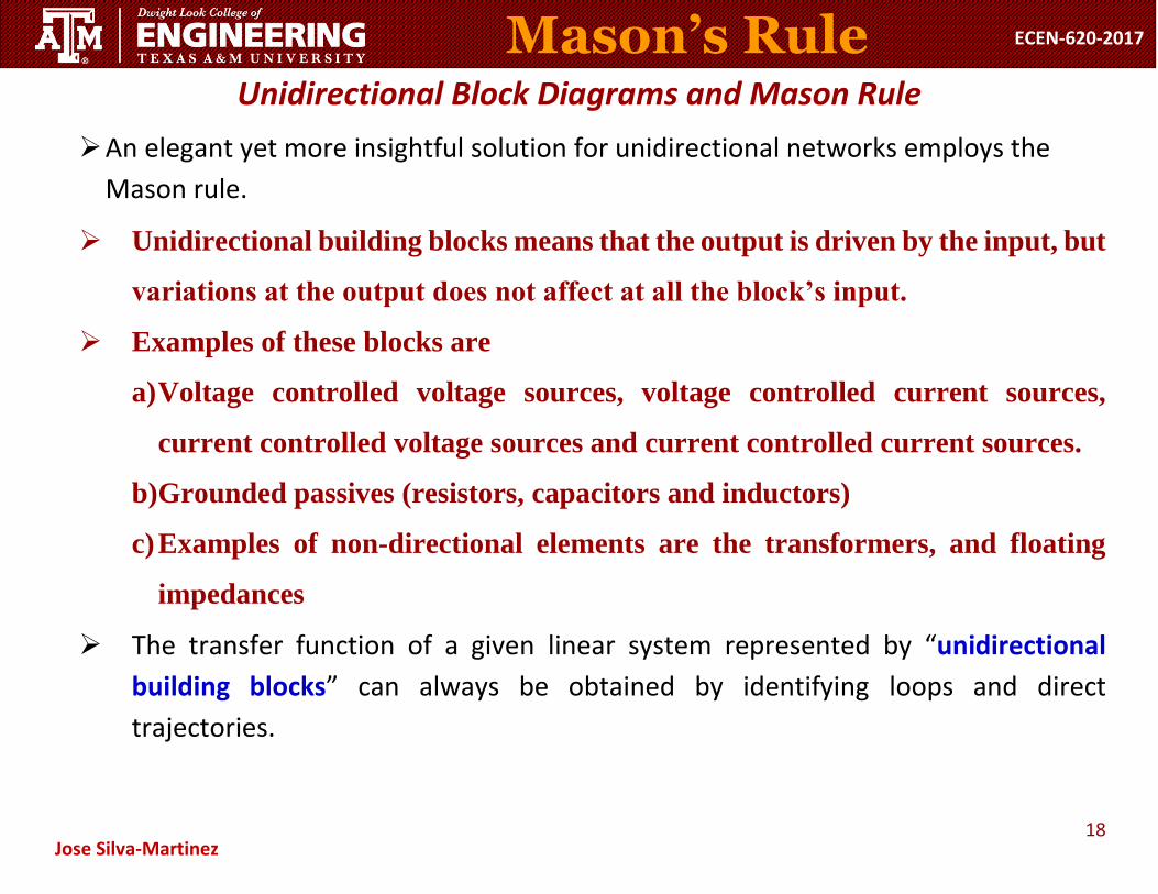
Unidirectional Block Diagrams and Mason Rule
An elegant yet more insightful solution for unidirectional networks employs the
Mason rule.
Unidirectional building blocks means that the output is driven by the input, but
variations at the output does not affect at all the block’s input.
Examples of these blocks are
a) Voltage controlled voltage sources, voltage controlled current sources,
current controlled voltage sources and current controlled current sources.
b) Grounded passives (resistors, capacitors and inductors)
c) Examples of non-directional elements are the transformers, and floating
impedances
The transfer function of a given linear system represented by “unidirectional
building blocks” can always be obtained by identifying loops and direct
trajectories.
Mason’s Rule
19
ECEN-620-2017
Jose Silva-Martinez
Once the system is represented by unidirectional elements, we must:
Identify the direct trajectories(paths) from the input(s) to output
KyAn(s) from Vy to output
AmAn from Vx to output
The loops must also be
identified
Am(s)
Loops that are not touched by certain direct paths; e.g.
The loop is not touched by the direct path KyAn
The loops that are not sharing elements or nodes (un-touched loops) have to be
identified. In this case we do not find any of these loops.
Feedback Properties
S An(s)SAm(s)
KyVy
Vx Vo
20
ECEN-620-2017
Jose Silva-Martinez
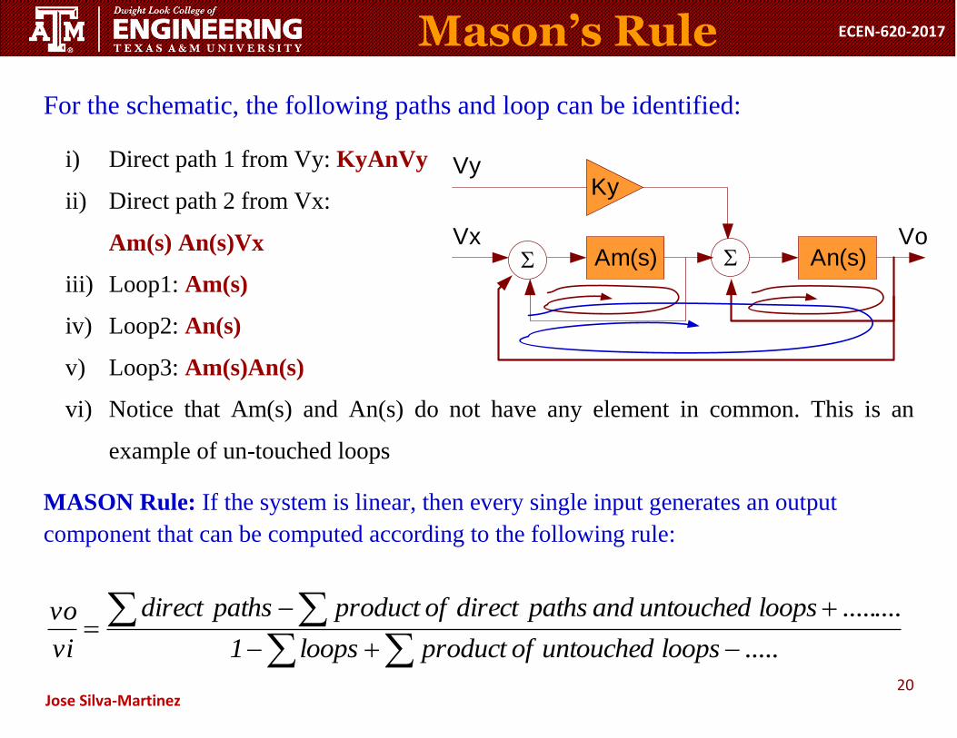
For the schematic, the following paths and loop can be identified:
i) Direct path 1 from Vy: KyAnVy
ii) Direct path 2 from Vx:
Am(s) An(s)Vx
iii) Loop1: Am(s)
iv) Loop2: An(s)
v) Loop3: Am(s)An(s)
vi) Notice that Am(s) and An(s) do not have any element in common. This is an
example of un-touched loops
MASON Rule: If the system is linear, then every single input generates an output
component that can be computed according to the following rule:
.....loopsuntouchedofproductloops1
.........loopsuntouchedandpathsdirectofproductpathsdirect
vi
vo
Mason’s Rule
S An(s)SAm(s)
KyVy
Vx Vo
21
ECEN-620-2017
Jose Silva-Martinez
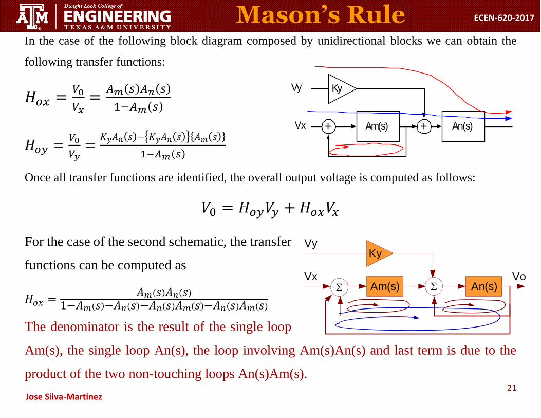
In the case of the following block diagram composed by unidirectional blocks we can obtain the
following transfer functions:
𝐻𝑜𝑥 =𝑉0
𝑉𝑥=𝐴𝑚(𝑠)𝐴𝑛(𝑠)
1−𝐴𝑚(𝑠)
𝐻𝑜𝑦 =𝑉0
𝑉𝑦=
𝐾𝑦𝐴𝑛(𝑠)−{𝐾𝑦𝐴𝑛(𝑠)}{𝐴𝑚(𝑠)}
1−𝐴𝑚(𝑠)
Once all transfer functions are identified, the overall output voltage is computed as follows:
𝑉0 = 𝐻𝑜𝑦𝑉𝑦 +𝐻𝑜𝑥𝑉𝑥
For the case of the second schematic, the transfer
functions can be computed as
𝐻𝑜𝑥 =𝐴𝑚(𝑠)𝐴𝑛(𝑠)
1−𝐴𝑚(𝑠)−𝐴𝑛(𝑠)−𝐴𝑛(𝑠)𝐴𝑚(𝑠)−𝐴𝑛(𝑠)𝐴𝑚(𝑠)
The denominator is the result of the single loop
Am(s), the single loop An(s), the loop involving Am(s)An(s) and last term is due to the
product of the two non-touching loops An(s)Am(s).
Am(s) An(s)+ +Vx
Vy Ky
loop is not touchedby Vy path
Am(s) An(s)+ +Vx
Vy Ky
Untouched loops
Mason’s Rule
S An(s)SAm(s)
KyVy
Vx Vo
22
ECEN-620-2017
Jose Silva-Martinez
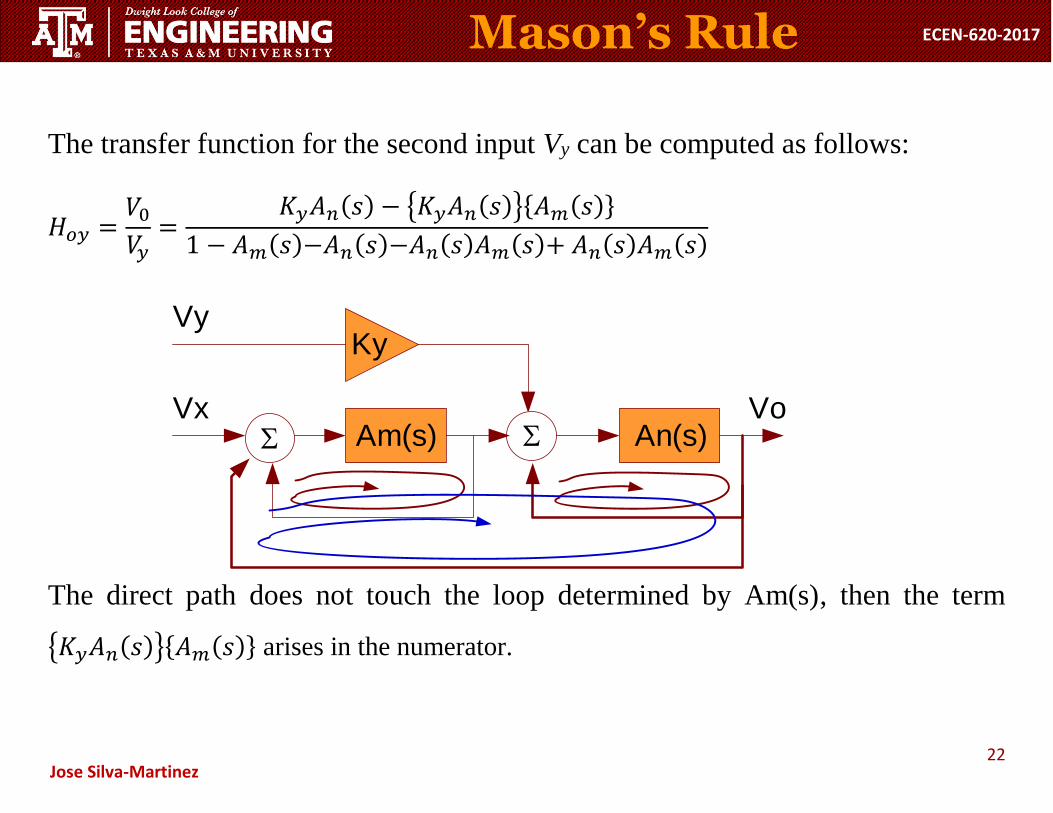
The transfer function for the second input Vy can be computed as follows:
𝐻𝑜𝑦 =𝑉0𝑉𝑦=
𝐾𝑦𝐴𝑛(𝑠) − {𝐾𝑦𝐴𝑛(𝑠)}{𝐴𝑚(𝑠)}
1 − 𝐴𝑚(𝑠)−𝐴𝑛(𝑠)−𝐴𝑛(𝑠)𝐴𝑚(𝑠)+ 𝐴𝑛(𝑠)𝐴𝑚(𝑠)
The direct path does not touch the loop determined by Am(s), then the term
{𝐾𝑦𝐴𝑛(𝑠)}{𝐴𝑚(𝑠)} arises in the numerator.
Mason’s Rule
S An(s)SAm(s)
KyVy
Vx Vo
23
ECEN-620-2017
Jose Silva-Martinez
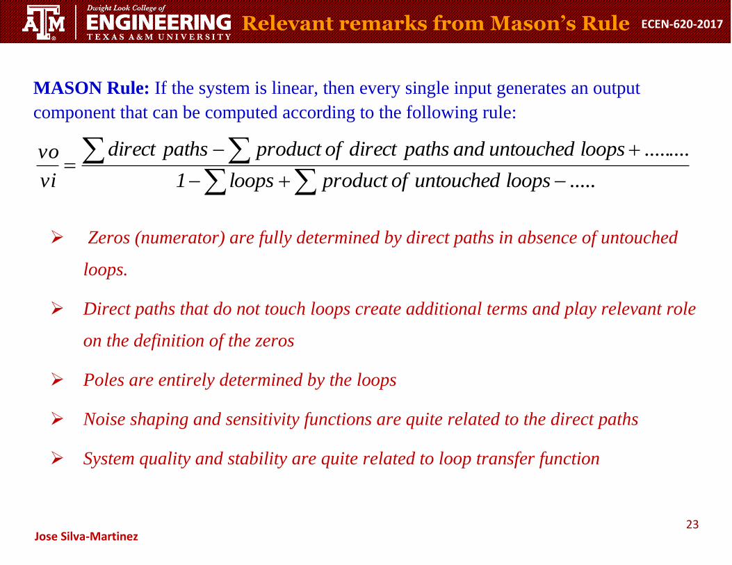
MASON Rule: If the system is linear, then every single input generates an output
component that can be computed according to the following rule:
.....loopsuntouchedofproductloops1
.........loopsuntouchedandpathsdirectofproductpathsdirect
vi
vo
Zeros (numerator) are fully determined by direct paths in absence of untouched
loops.
Direct paths that do not touch loops create additional terms and play relevant role
on the definition of the zeros
Poles are entirely determined by the loops
Noise shaping and sensitivity functions are quite related to the direct paths
System quality and stability are quite related to loop transfer function
Relevant remarks from Mason’s Rule
24
ECEN-620-2017
Jose Silva-Martinez
See some examples related to Sigma-Delta Modulators
25
ECEN-620-2017
Jose Silva-Martinez
Sensitivity Function
When dealing with multivariable functions and when some of the parameters may have
significant variations then it is useful to compute the sensitivity functions to quantify
the individual variability effects on system performance.
The sensitivity of a multivariable function H(x, y, z, …) as function of the parameter
x is defined as
∫𝐻
𝑥= (
𝑥
𝐻) (
𝑑𝐻
𝑑𝑥) =
(𝑑𝐻
𝑑𝑥)
𝐻
𝑥
or 𝑑𝐻
𝐻= ∫ (
𝑑𝑋
𝑋)
𝐻
𝑥
The sensitivity function represents the first order variation of H as function of
the parameter x, normalized by the factor H/x.
Properties of Sensitivity Function
26
ECEN-620-2017
Jose Silva-Martinez
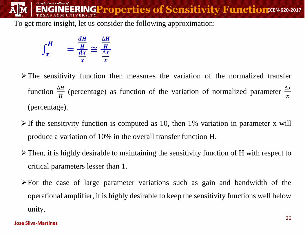
To get more insight, let us consider the following approximation:
∫𝑯
𝒙=
𝒅𝑯
𝑯𝒅𝒙
𝒙
≅∆𝑯
𝑯∆𝒙
𝒙
The sensitivity function then measures the variation of the normalized transfer
function ∆𝐻
𝐻 (percentage) as function of the variation of normalized parameter
∆𝑥
𝑥
(percentage).
If the sensitivity function is computed as 10, then 1% variation in parameter x will
produce a variation of 10% in the overall transfer function H.
Then, it is highly desirable to maintaining the sensitivity function of H with respect to
critical parameters lesser than 1.
For the case of large parameter variations such as gain and bandwidth of the
operational amplifier, it is highly desirable to keep the sensitivity functions well below
unity.
Properties of Sensitivity Function
27
ECEN-620-2017
Jose Silva-Martinez
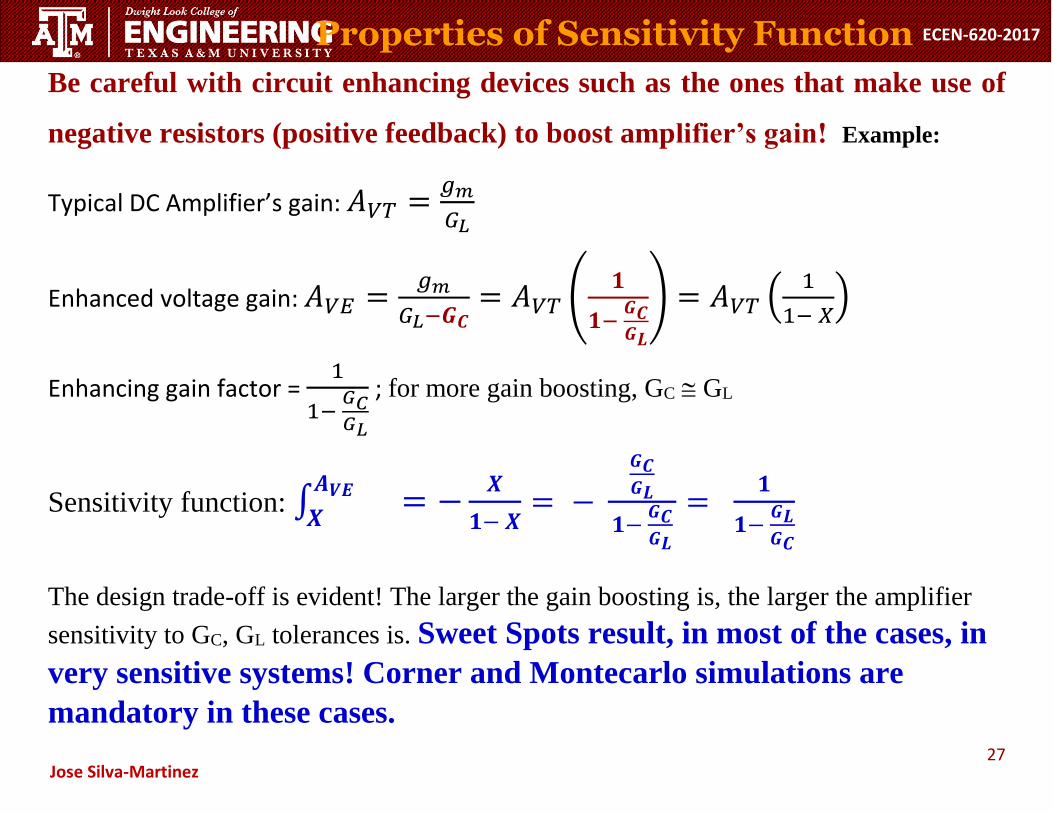
Be careful with circuit enhancing devices such as the ones that make use of
negative resistors (positive feedback) to boost amplifier’s gain! Example:
Typical DC Amplifier’s gain: 𝐴𝑉𝑇 =𝑔𝑚
𝐺𝐿
Enhanced voltage gain: 𝐴𝑉𝐸 =𝑔𝑚
𝐺𝐿−𝑮𝑪= 𝐴𝑉𝑇 (
𝟏
𝟏− 𝑮𝑪𝑮𝑳
) = 𝐴𝑉𝑇 (1
1− 𝑋)
Enhancing gain factor = 1
1− 𝐺𝐶𝐺𝐿
; for more gain boosting, GC GL
Sensitivity function: ∫𝑨𝑽𝑬
𝑿= −
𝑿
𝟏− 𝑿= −
𝑮𝑪𝑮𝑳
𝟏− 𝑮𝑪𝑮𝑳
= 𝟏
𝟏− 𝑮𝑳𝑮𝑪
The design trade-off is evident! The larger the gain boosting is, the larger the amplifier
sensitivity to GC, GL tolerances is. Sweet Spots result, in most of the cases, in
very sensitive systems! Corner and Montecarlo simulations are
mandatory in these cases.
Properties of Sensitivity Function
28
ECEN-620-2017
Jose Silva-Martinez
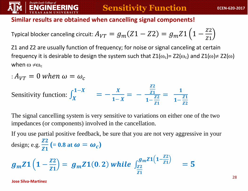
Similar results are obtained when cancelling signal components!
Typical blocker canceling circuit: 𝐴𝑉𝑇 = 𝑔𝑚(𝑍1 − 𝑍2) = 𝑔𝑚𝑍1 (1 −𝑍2
𝑍1)
Z1 and Z2 are usually function of frequency; for noise or signal canceling at certain
frequency it is desirable to design the system such that Z1(c)= Z2(c) and Z1() Z2()
when c
: 𝐴𝑉𝑇 = 0 𝑤ℎ𝑒𝑛 𝜔 = 𝜔𝑐
Sensitivity function: ∫𝟏−𝑿
𝑿= −
𝑿
𝟏− 𝑿= −
𝒁𝟐
𝒁𝟏
𝟏− 𝒁𝟐
𝒁𝟏
= 𝟏
𝟏− 𝒁𝟏
𝒁𝟐
The signal cancelling system is very sensitive to variations on either one of the two
impedances (or components) involved in the cancellation.
If you use partial positive feedback, be sure that you are not very aggressive in your
design; e.g. 𝒁𝟐
𝒁𝟏 (= 0.8 at 𝝎 = 𝝎𝒄)
𝒈𝒎𝒁𝟏 (𝟏 −𝒁𝟐
𝒁𝟏) = 𝒈𝒎𝒁𝟏(𝟎. 𝟐) 𝒘𝒉𝒊𝒍𝒆 ∫
𝒈𝒎𝒁𝟏(𝟏−𝒁𝟐
𝒁𝟏)
𝒁𝟐
𝒁𝟏
= 𝟓
Sensitivity Function
29
ECEN-620-2017
Jose Silva-Martinez
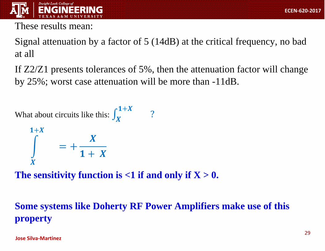
These results mean:
Signal attenuation by a factor of 5 (14dB) at the critical frequency, no bad
at all
If Z2/Z1 presents tolerances of 5%, then the attenuation factor will change
by 25%; worst case attenuation will be more than -11dB.
What about circuits like this: ∫𝟏+𝑿
𝑿 ?
∫
𝟏+𝑿
𝑿
= +𝑿
𝟏 + 𝑿
The sensitivity function is <1 if and only if X > 0.
Some systems like Doherty RF Power Amplifiers make use of this
property
30
ECEN-620-2017
Jose Silva-Martinez
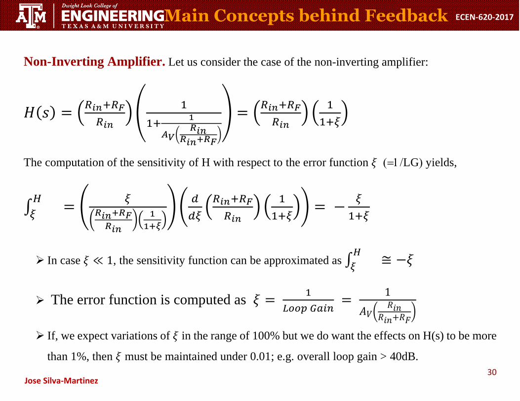
Non-Inverting Amplifier. Let us consider the case of the non-inverting amplifier:
𝐻(𝑠) = (𝑅𝑖𝑛+𝑅𝐹
𝑅𝑖𝑛)(
1
1+1
𝐴𝑉(𝑅𝑖𝑛
𝑅𝑖𝑛+𝑅𝐹)
) = (𝑅𝑖𝑛+𝑅𝐹
𝑅𝑖𝑛) (
1
1+𝜉)
The computation of the sensitivity of H with respect to the error function 𝜉LGyields,
∫𝐻
𝜉= (
𝜉
(𝑅𝑖𝑛+𝑅𝐹𝑅𝑖𝑛
)(1
1+𝜉))(
𝑑
𝑑𝜉(𝑅𝑖𝑛+𝑅𝐹
𝑅𝑖𝑛) (
1
1+𝜉)) = −
𝜉
1+𝜉
In case 𝜉 ≪ 1, the sensitivity function can be approximated as ∫𝐻
𝜉≅ −𝜉
The error function is computed as 𝜉 = 1
𝐿𝑜𝑜𝑝 𝐺𝑎𝑖𝑛 =
1
𝐴𝑉(𝑅𝑖𝑛
𝑅𝑖𝑛+𝑅𝐹)
If, we expect variations of 𝜉 in the range of 100% but we do want the effects on H(s) to be more
than 1%, then 𝜉 must be maintained under 0.01; e.g. overall loop gain > 40dB.
Main Concepts behind Feedback
31
ECEN-620-2017
Jose Silva-Martinez
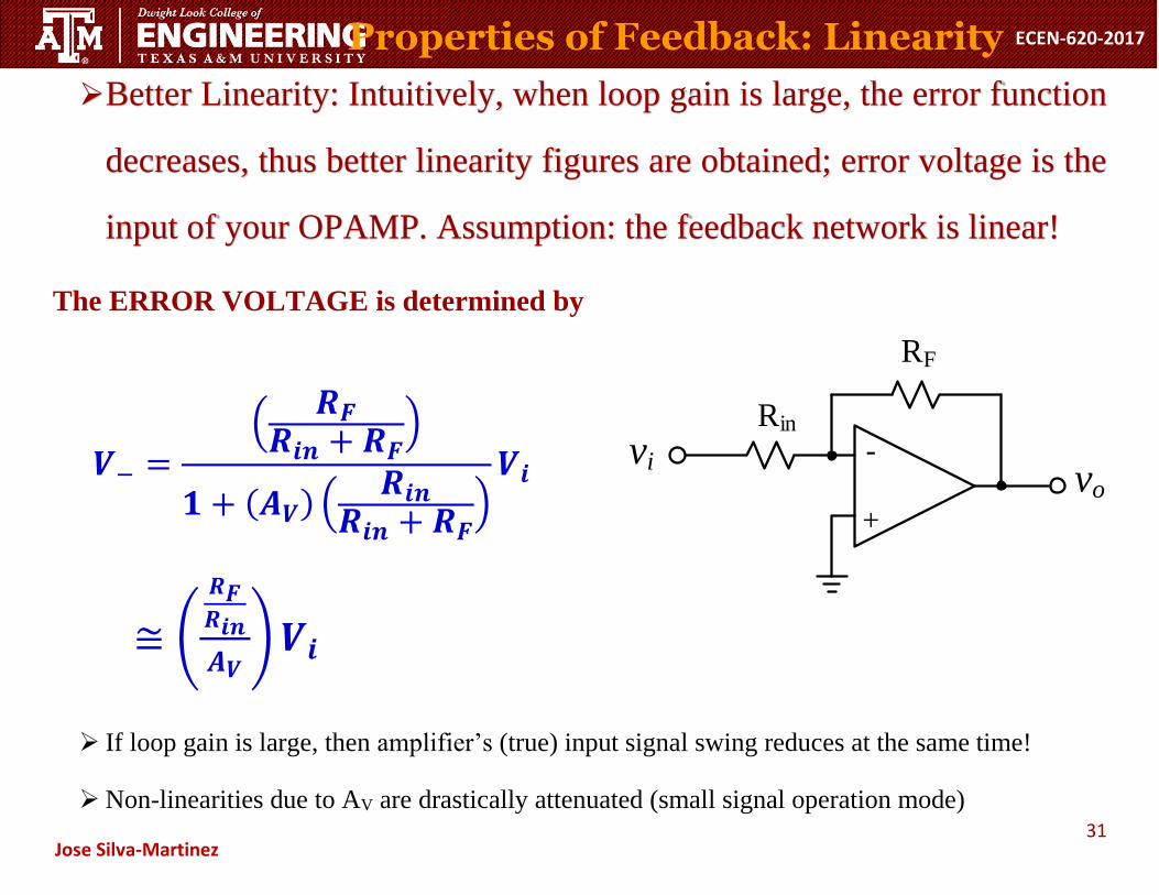
Better Linearity: Intuitively, when loop gain is large, the error function
decreases, thus better linearity figures are obtained; error voltage is the
input of your OPAMP. Assumption: the feedback network is linear!
The ERROR VOLTAGE is determined by
𝑽− =(
𝑹𝑭𝑹𝒊𝒏 + 𝑹𝑭
)
𝟏 + (𝑨𝑽) (𝑹𝒊𝒏
𝑹𝒊𝒏 + 𝑹𝑭)𝑽𝒊
≅ (
𝑹𝑭𝑹𝒊𝒏
𝑨𝑽)𝑽𝒊
If loop gain is large, then amplifier’s (true) input signal swing reduces at the same time!
Non-linearities due to AV are drastically attenuated (small signal operation mode)
+
-
vo
RF
Rin
vi
Properties of Feedback: Linearity
32
ECEN-620-2017
Jose Silva-Martinez
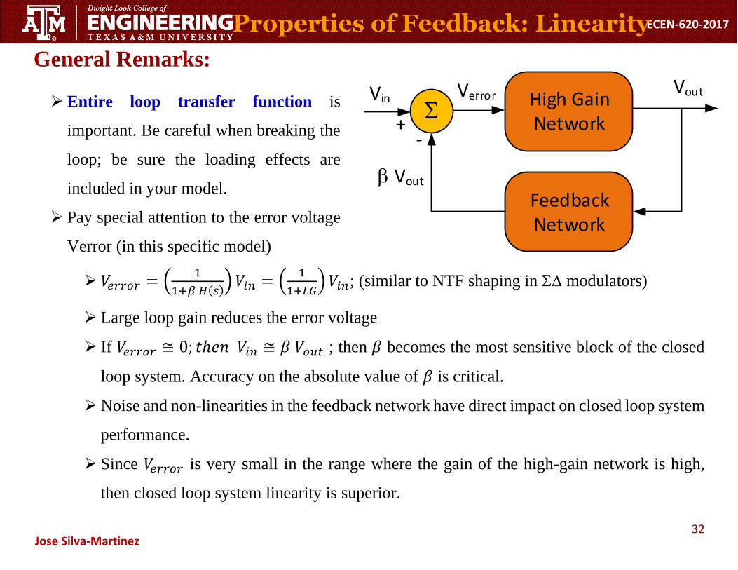
General Remarks:
Entire loop transfer function is
important. Be careful when breaking the
loop; be sure the loading effects are
included in your model.
Pay special attention to the error voltage
Verror (in this specific model)
𝑉𝑒𝑟𝑟𝑜𝑟 = (1
1+𝛽 𝐻(𝑠))𝑉𝑖𝑛 = (
1
1+𝐿𝐺)𝑉𝑖𝑛; (similar to NTF shaping in S modulators)
Large loop gain reduces the error voltage
If 𝑉𝑒𝑟𝑟𝑜𝑟 ≅ 0; 𝑡ℎ𝑒𝑛 𝑉𝑖𝑛 ≅ 𝛽 𝑉𝑜𝑢𝑡 ; then 𝛽 becomes the most sensitive block of the closed
loop system. Accuracy on the absolute value of 𝛽 is critical.
Noise and non-linearities in the feedback network have direct impact on closed loop system
performance.
Since 𝑉𝑒𝑟𝑟𝑜𝑟 is very small in the range where the gain of the high-gain network is high,
then closed loop system linearity is superior.
High Gain Network
SVerror
Feedback Network
VinVout
+-
Vout
Properties of Feedback: Linearity
33
ECEN-620-2017
Jose Silva-Martinez
Linearity improves if and only if LG is large.
If LG is small, then 𝑉𝑒𝑟𝑟𝑜𝑟 ≈ 𝑉𝑖𝑛 then the high-gain network has to manage the entire input
signal range; but OPAMPs are non-linear. Large signal non-linearities are quite large and
usually can not be tolerated.
𝑉𝑜𝑢𝑡 = (𝐻(𝑠)
1+𝛽 𝐻(𝑠))𝑉𝑖𝑛
𝑉𝑜𝑢𝑡 ≅ (1
𝛽)𝑉𝑖𝑛 𝑖𝑓 1 ≪ 𝛽𝐻(𝑠)
𝑉𝑜𝑢𝑡 ≅ (𝐻(𝑠))𝑉𝑖𝑛 𝑖𝑓 1 > 𝛽𝐻(𝑠)
On top of this, since this is a closed loop system 𝐿𝐺 = 𝛽 𝐻(𝑠) is critical for loop stability.
Phase margin is relevant to avoid excessive closed loop peaking.
Properties of Feedback: Linearity

34
ECEN-620-2017
Jose Silva-Martinez
Root Locus provides more information on system stability. Root locus show how open-
loop poles move when the loop is closed and 𝛽 changes
How the poles move when feedback factor changes?
How stability is affected if poles and zeros move with process variations?
35
ECEN-620-2017
Jose Silva-Martinez
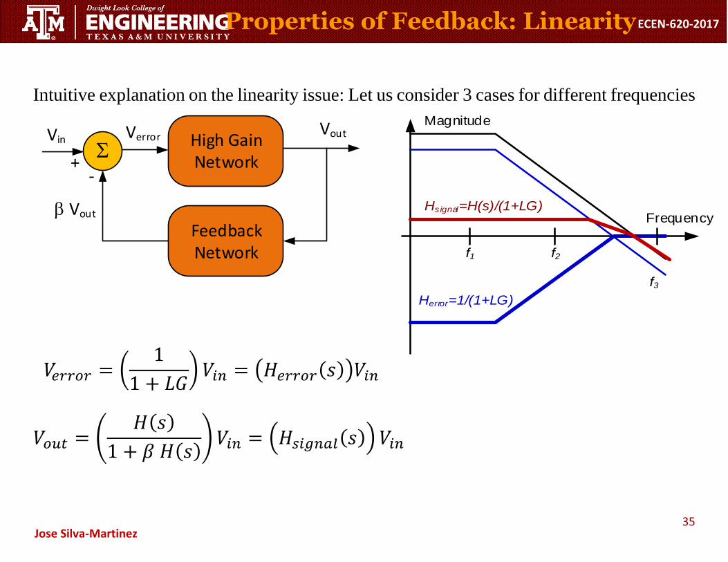
Intuitive explanation on the linearity issue: Let us consider 3 cases for different frequencies
𝑉𝑒𝑟𝑟𝑜𝑟 = (1
1 + 𝐿𝐺)𝑉𝑖𝑛 = (𝐻𝑒𝑟𝑟𝑜𝑟(𝑠))𝑉𝑖𝑛
𝑉𝑜𝑢𝑡 = (𝐻(𝑠)
1 + 𝛽 𝐻(𝑠))𝑉𝑖𝑛 = (𝐻𝑠𝑖𝑔𝑛𝑎𝑙(𝑠)) 𝑉𝑖𝑛
High Gain Network
SVerror
Feedback Network
VinVout
+-
Vout
Properties of Feedback: Linearity
Herror=1/(1+LG)
f1 f2
f3
Magnitude
FrequencyHsignal=H(s)/(1+LG)
36
ECEN-620-2017
Jose Silva-Martinez
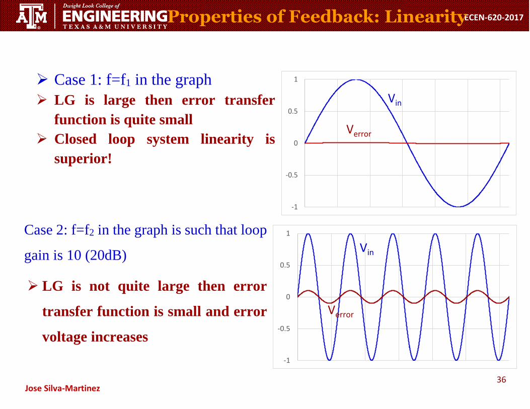
Case 1: f=f1 in the graph
LG is large then error transfer
function is quite small
Closed loop system linearity is
superior!
Case 2: f=f2 in the graph is such that loop
gain is 10 (20dB)
LG is not quite large then error
transfer function is small and error
voltage increases
-1
-0.5
0
0.5
1
Vin
Verror
-1
-0.5
0
0.5
1
Vin
Verror
Properties of Feedback: Linearity
37
ECEN-620-2017
Jose Silva-Martinez
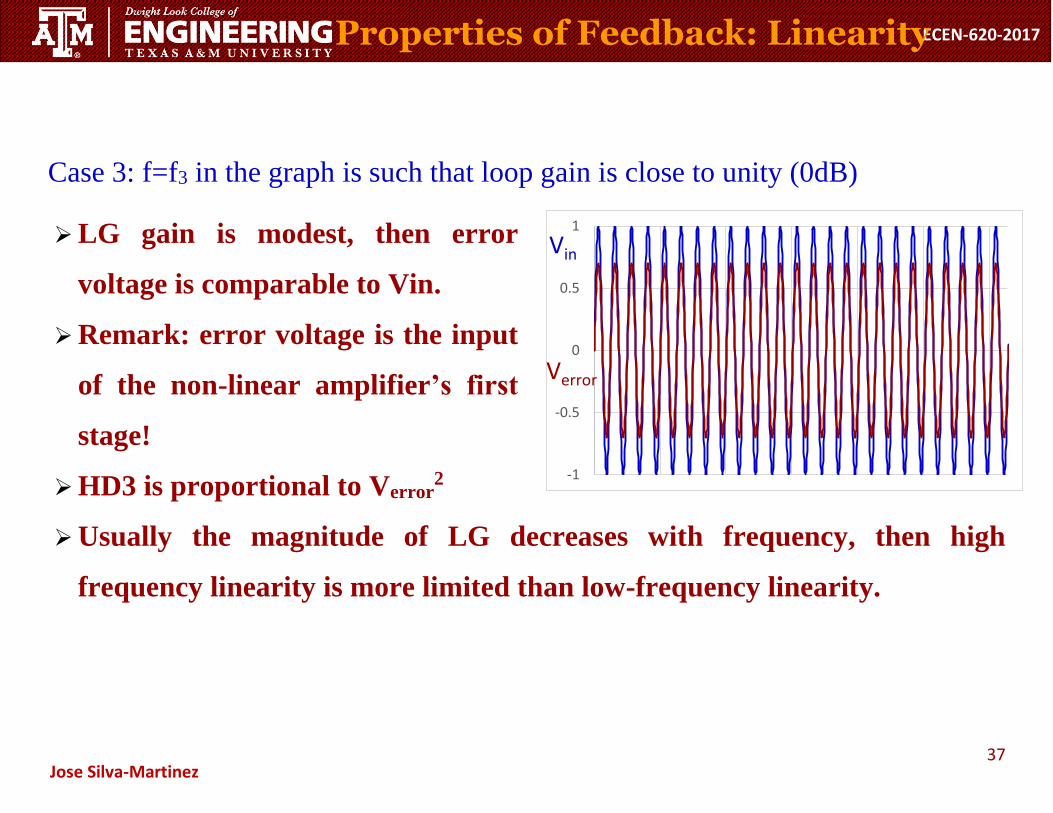
Case 3: f=f3 in the graph is such that loop gain is close to unity (0dB)
LG gain is modest, then error
voltage is comparable to Vin.
Remark: error voltage is the input
of the non-linear amplifier’s first
stage!
HD3 is proportional to Verror2
Usually the magnitude of LG decreases with frequency, then high
frequency linearity is more limited than low-frequency linearity.
-1
-0.5
0
0.5
1
Vin
Verror
Properties of Feedback: Linearity
38
ECEN-620-2017
Jose Silva-Martinez
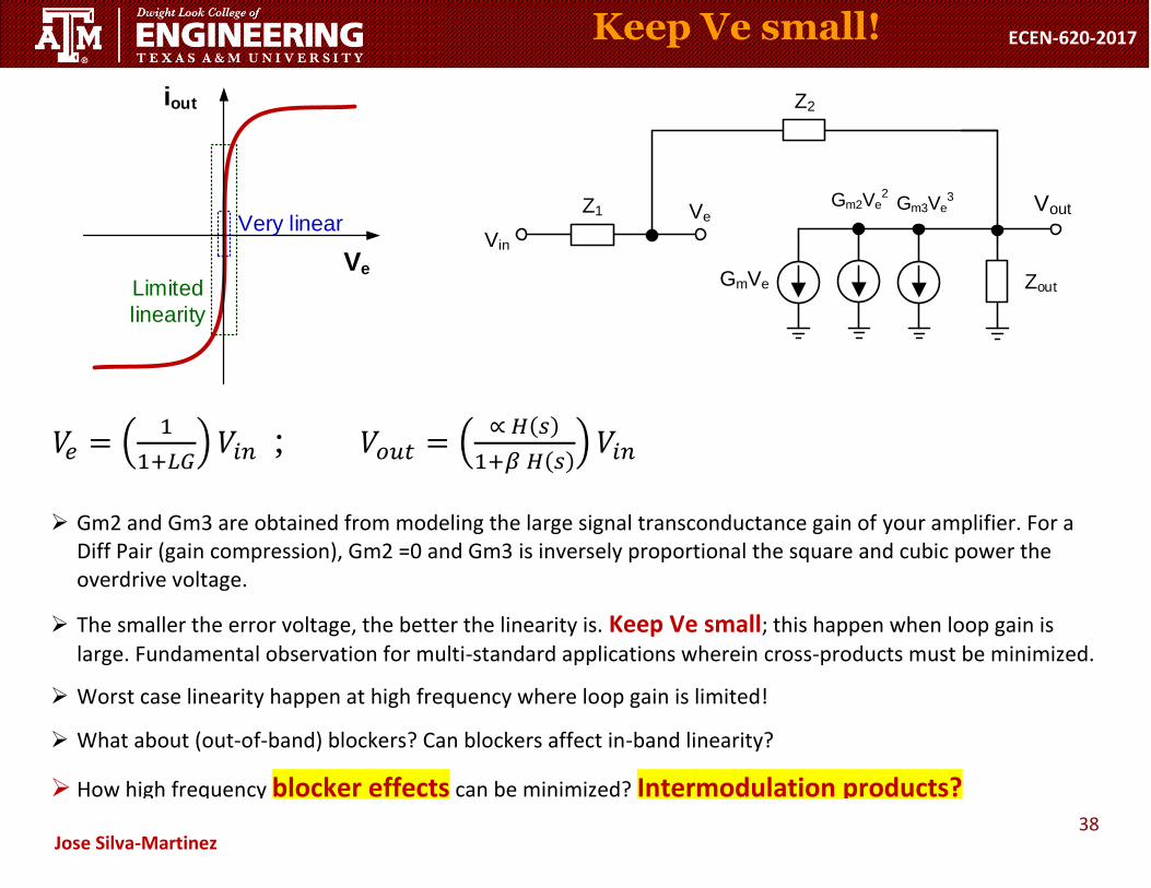
𝑉𝑒 = (1
1+𝐿𝐺)𝑉𝑖𝑛 ; 𝑉𝑜𝑢𝑡 = (
∝ 𝐻(𝑠)
1+𝛽 𝐻(𝑠))𝑉𝑖𝑛
Z1
Vin
Zout
VeVout
Gm2Ve2
GmVe
Gm3Ve3
Z2
Gm2 and Gm3 are obtained from modeling the large signal transconductance gain of your amplifier. For a Diff Pair (gain compression), Gm2 =0 and Gm3 is inversely proportional the square and cubic power the overdrive voltage.
The smaller the error voltage, the better the linearity is. Keep Ve small; this happen when loop gain is
large. Fundamental observation for multi-standard applications wherein cross-products must be minimized.
Worst case linearity happen at high frequency where loop gain is limited!
What about (out-of-band) blockers? Can blockers affect in-band linearity?
How high frequency blocker effects can be minimized? Intermodulation products?
iout
Ve
Very linear
Limited
linearity
Keep Ve small!
39
ECEN-620-2017
Jose Silva-Martinez
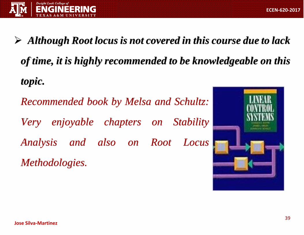
Although Root locus is not covered in this course due to lack
of time, it is highly recommended to be knowledgeable on this
topic.
Recommended book by Melsa and Schultz:
Very enjoyable chapters on Stability
Analysis and also on Root Locus
Methodologies.