Embed Size (px)
Citation preview
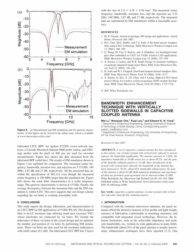
fabricated LTCC BPF. An Agilent 8722ES vector network ana-lyzer, a Cascade Microtech Summit 9000 probe station, and GSG-type probes with the pitch of 400 �m are used for on-wafermeasurements. Figure 6(a) shows the data measured from thefabricated BPF (solid line). The results of EM simulation shown inFigure 4 are replotted for comparison. The measured center fre-quency, bandwidth, insertion loss, and rejection are 5.32 GHz, 340MHz, 2.87 dB, and 27 dB, respectively. All the measured data arewithin the specification of 802.11a even though the measuredcenter frequency is 100 MHz larger than the simulated one. Figure6(b) shows the same filter characteristics in a wider frequencyrange. The spurious characteristic is shown at 13 GHz. Finally, theaverage discrepancy between the measured data and the EM sim-ulation is within 6.0%. This error suggests that our design schemeregarding the via holes is working reasonably well.
5. CONCLUSIONS
This study reports the design, fabrication, and characterization ofan LTCC BPF for SiP applications of 5 GHz WLAN. The designedfilter is an LC resonator type utilizing small area resonator VICswhose electrodes are connected by via holes. We include theinductance of these via holes in the circuit design and we optimizethe number and position of via holes by performing EM simula-tions. These via holes are also used for the resonator inductanceswith small values (0.1 nH). The fabricated LTCC BPF has 5 layers
with the size of 2.4 � 4.18 � 0.56 mm3. The measured centerfrequency, bandwidth, insertion loss, and the rejection are 5.32GHz, 340 MHz, 2.87 dB, and 27 dB, respectively. The measureddata are reproduced by EM simulations within a reasonable accu-racy.
REFERENCES
1. M. P. Gaynor, System-in-package: RF design and applications, ArtechHouse, Norwood, MA 2007.
2. B.G. Choi, M.G. Stubbs, and C.S. Park, A Ka-band narrow bandpassfilter using LTCC technology, IEEE Microwave Wireless Compon Lett13 (2003), 388–389.
3. G. Wang, M. Van, F. Barlow, and A. Elshabini, An interdigital band-pass filter embedded in LTCC for 5-GHz wireless LAN applications,IEEE Microwave Wireless Compon Lett 15 (2005), 357–359.
4. A. Sutono, J. Laskar, and W.R. Smith, Design of miniature multilayeron-package integrated image-reject filters, IEEE Trans Microwave The-ory Tech 51 (2003), 156–162.
5. H. Joshi and W.J. Chappell, Dual-band lumped-element bandpass filter,IEEE Trans Microwave Theory Tech 54 (2006), 4169–4177.
6. A. Sutono, D. Heo, Y.-J.E. Chen, and J. Laskar, High-Q LTCC-basedpassive library for wireless system-on-package (SOP) module develop-ment, IEEE Trans Microwave Theory Tech 49 (2001), 1715–1724.
© 2007 Wiley Periodicals, Inc.
BANDWIDTH ENHANCEMENTTECHNIQUE WITH VERTICALLYSLOTTED SIDEWALLS IN CAPACITIVECOUPLED ANTENNA
Mei Li,1 Wenquan Che,1 Puiyi Lau,2 and Edward K. N. Yung2
1 Department of Electrical Engineering, Nanjing University of Science& Technology 210094 Nanjing, China; Corresponding author:[email protected] Department of Electronic Engineering, City University of Hong Kong,83 Tat Chee Avenue, Kowloon, Hong Kong
Received 25 June 2007
ABSTRACT: A novel capacitive coupled antenna has been introducedin this article; one circular ground with vertical-slots sidewall is used toimprove the bandwidth significantly. The antenna operates at 3 GHz, theimpedance bandwidth at 10-dB return loss is about 48.2%, and the gainof the butterfly radiation pattern is 3.8 dB. After introduction of theground with vertical-slots sidewall, the bandwidth of the antenna hasbeen improved to 78.2%, about 62% bandwidth enhancement; the gainof this antenna is about 6.0 dB. Both numerical simulations and experimen-tal data are presented, good agreement can be observed within. © 2007Wiley Periodicals, Inc. Microwave Opt Technol Lett 50: 341–345, 2008;Published online in Wiley InterScience (www.interscience.wiley.com).DOI 10.1002/mop.23066
Key words: capacitive coupled antenna; circular ground with vertical-slot sidewalls; butterfly-like radiation pattern
1. INTRODUCTION
Compared with the common microwave antennas, the patch an-tennas afford the attractive features of low profile and light weight,easiness of fabrication, conformable to mounting structures, andcompatible with integrated circuit technology. However, the in-herent limitations, such as the achievable impedance and axial-ratio bandwidths, etc., restrain its wide applications in many fields.The bandwidth (about 5%) of the patch antenna is usually narrow;many enhancement techniques have been reported [1-3]. One
Figure 6 (a) Measurement and EM simulation and (b) spurious charac-teristic. [Color figure can be viewed in the online issue, which is availableat www.interscience.wiley.com]
DOI 10.1002/mop MICROWAVE AND OPTICAL TECHNOLOGY LETTERS / Vol. 50, No. 2, February 2008 341
U-slot patch [1] was used to increase the bandwidth to 30%, andL-probe feeding could also enhance the bandwidth to 35% [2]. Thebandwidth of a probe-fed microstrip antenna is limited by theinductance introduced by the coaxial feed. A circular patch mi-crostrip antenna with a top-loaded monopole feed was ever inves-tigated [3] and the impedance bandwidth reaches to 26.8%. In thiswork, an additional radiation element is introduced on the lowerpatch. As a matter of fact, the upper element and the lower patchforms a parallel-plate capacitor, a capacitance is then introduced tocancel out the probe inductance, resulting in more than 48%impedance bandwidth (SWR � 2). In addition, one circular groundwith vertical-slots sidewall is employed. As a result, the imped-ance bandwidth (SWR � 2) reaches 78.2%, demonstrating morethan 60% bandwidth improvement.
2. ANTENNA DESIGN CONSIDERATION
As we know, the monopole antenna is one kind of vertical polar-ized antennas and takes advantages of simple structure and wideimpedance bandwidth [4]. However, it has a drawback of thickprofile (about 0.25 �0). On the other hand, the patch antenna isattractive for its low profile. As we know, the microstrip patchantenna is equivalent to a simple monopole [5], which can providea monopole radiated pattern, when the patch antenna operating atTM01 mode is fed with probe located at the center of the patch. Inthis work, a patch antenna with centrally fed probe and capacitive-load element has been introduced; the ground with vertical-slotsidewalls is used also to enhance the bandwidth significantly.
In general, the resonant length of the patch antenna operating atTM01 mode is about one wavelength; it is too large for manyapplications. In this way, the size reduction is necessary for savingspace. There are many size reduction techniques for patch anten-nas, such as meander strip patch [6] and introduction of shortingpins [7], etc. In this work, a radiation element is introduced insteadof the top-loaded patch and the vertical sidewalls are added to thetop patch to increase the bandwidth. The upper radiation elementand the lower patch form a parallel-plate capacitor, which intro-duces a capacitance to cancel out the probe inductance and thusresulting in wider bandwidth. For the sake of size reduction, fourmetal strips are used to replace the metal poles connected betweenthe radiation element and the ground. Because of the four metalstrips, the size of the antenna can be reduced to 1/3 of the originaldesign.
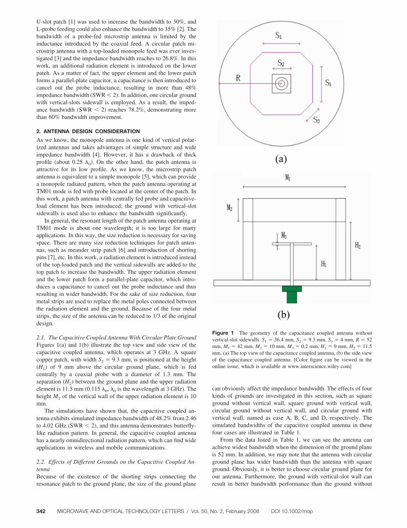
2.1. The Capacitive Coupled Antenna With Circular Plate GroundFigures 1(a) and 1(b) illustrate the top view and side view of thecapacitive coupled antenna, which operates at 3 GHz. A squarecopper patch, with width S2 � 9.3 mm, is positioned at the height(H1) of 9 mm above the circular ground plane, which is fedcentrally by a coaxial probe with a diameter of 1.3 mm. Theseparation (H2) between the ground plane and the upper radiationelement is 11.5 mm (0.115 �0, �0 is the wavelength at 3 GHz). Theheight M2 of the vertical wall of the upper radiation element is 10mm.
The simulations have shown that, the capacitive coupled an-tenna exhibits simulated impedance bandwidth of 48.2% from 2.46to 4.02 GHz (SWR � 2), and this antenna demonstrates butterfly-like radiation pattern. In general, the capacitive coupled antennahas a nearly omnidirectional radiation pattern, which can find wideapplications in wireless and mobile communications.
2.2. Effects of Different Grounds on the Capacitive Coupled An-tennaBecause of the existence of the shorting strips connecting theresonance patch to the ground plane, the size of the ground plane
can obviously affect the impedance bandwidth. The effects of fourkinds of grounds are investigated in this section, such as squareground without vertical wall, square ground with vertical wall,circular ground without vertical wall, and circular ground withvertical wall, named as case A, B, C, and D, respectively. Thesimulated bandwidths of the capacitive coupled antenna in thesefour cases are illustrated in Table 1.
From the data listed in Table 1, we can see the antenna canachieve widest bandwidth when the dimension of the ground planeis 52 mm. In addition, we may note that the antenna with circularground plane has wider bandwidth than the antenna with squareground. Obviously, it is better to choose circular ground plane forour antenna. Furthermore, the ground with vertical-slot wall canresult in better bandwidth performance than the ground without
Figure 1 The geometry of the capacitance coupled antenna withoutvertical-slot sidewalls. S1 � 36.4 mm, S2 � 9.3 mm, S3 � 4 mm, R � 52mm, M1 � 42 mm, M2 � 10 mm, M3 � 0.2 mm, H1 � 9 mm, H2 � 11.5mm. (a) The top view of the capacitance coupled antenna, (b) the side viewof the capacitance coupled antenna. [Color figure can be viewed in theonline issue, which is available at www.interscience.wiley.com]
342 MICROWAVE AND OPTICAL TECHNOLOGY LETTERS / Vol. 50, No. 2, February 2008 DOI 10.1002/mop
vertical-slot wall. For example, when R � 52 mm, the bandwidthin case A (rectangular ground without vertical-slot wall) is 48.2%,while the bandwidth in case B (rectangular ground without verti-cal-slot wall) is 52.8%. In this way, the ground with vertical-slotwall is used to improve the bandwidth of the capacitive coupledantenna proposed in subsection A. The geometries (top view andside view) are illustrated in Figures 2(a) and 2(b). Noting that, the
number of the slots is 24, i.e., the sidewall is divided into 24pieces. The height of the sidewall (H3) is 4 mm. The parameters ofthis antenna are the same with the capacitive coupled antennashown in Figure 1, except of the additional vertical sidewall to theground.
3. RESULTS AND DISCUSSIONS
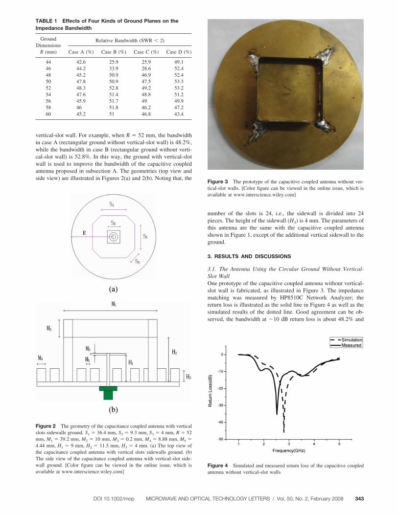
3.1. The Antenna Using the Circular Ground Without Vertical-Slot WallOne prototype of the capacitive coupled antenna without vertical-slot wall is fabricated, as illustrated in Figure 3. The impedancematching was measured by HP8510C Network Analyzer; thereturn loss is illustrated as the solid line in Figure 4 as well as thesimulated results of the dotted line. Good agreement can be ob-served, the bandwidth at �10 dB return loss is about 48.2% and
TABLE 1 Effects of Four Kinds of Ground Planes on theImpedance Bandwidth
GroundDimensions
R (mm)
Relative Bandwidth (SWR � 2)
Case A (%) Case B (%) Case C (%) Case D (%)
44 42.6 25.9 25.9 49.146 44.2 33.9 28.6 52.448 45.2 50.9 46.9 52.450 47.8 50.9 47.5 53.352 48.3 52.8 49.2 53.254 47.6 51.4 48.8 51.256 45.9 51.7 49 49.958 46 51.8 46.2 47.260 45.2 51 46.8 43.4
Figure 2 The geometry of the capacitance coupled antenna with verticalslots sidewalls ground. S1 � 36.4 mm, S2 � 9.3 mm, S3 � 4 mm, R � 52mm, M1 � 39.2 mm, M2 � 10 mm, M3 � 0.2 mm, M4 � 8.88 mm, M5 �4.44 mm, H1 � 9 mm, H2 � 11.5 mm, H3 � 4 mm. (a) The top view ofthe capacitance coupled antenna with vertical slots sidewalls ground. (b)The side view of the capacitance coupled antenna with vertical-slot side-wall ground. [Color figure can be viewed in the online issue, which isavailable at www.interscience.wiley.com]
Figure 3 The prototype of the capacitive coupled antenna without ver-tical-slot walls. [Color figure can be viewed in the online issue, which isavailable at www.interscience.wiley.com]
Figure 4 Simulated and measured return loss of the capacitive coupledantenna without vertical-slot walls
DOI 10.1002/mop MICROWAVE AND OPTICAL TECHNOLOGY LETTERS / Vol. 50, No. 2, February 2008 343
55.3%, respectively. In addition, the measured radiation patternsare shown in Figures 5(a) and 5(b) as the solid lines, in which thesimulated radiation patterns are also shown as the dotted lines.Obviously, good agreement can be observed, the simulated andmeasured gains of the capacitive coupled antenna are 3.8 dB and4.5 dB, respectively.
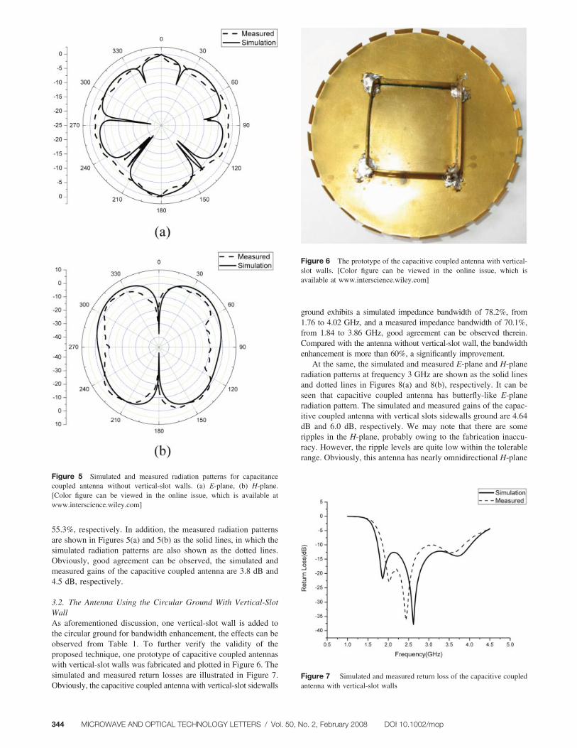
3.2. The Antenna Using the Circular Ground With Vertical-SlotWallAs aforementioned discussion, one vertical-slot wall is added tothe circular ground for bandwidth enhancement, the effects can beobserved from Table 1. To further verify the validity of theproposed technique, one prototype of capacitive coupled antennaswith vertical-slot walls was fabricated and plotted in Figure 6. Thesimulated and measured return losses are illustrated in Figure 7.Obviously, the capacitive coupled antenna with vertical-slot sidewalls
ground exhibits a simulated impedance bandwidth of 78.2%, from1.76 to 4.02 GHz, and a measured impedance bandwidth of 70.1%,from 1.84 to 3.86 GHz, good agreement can be observed therein.Compared with the antenna without vertical-slot wall, the bandwidthenhancement is more than 60%, a significantly improvement.
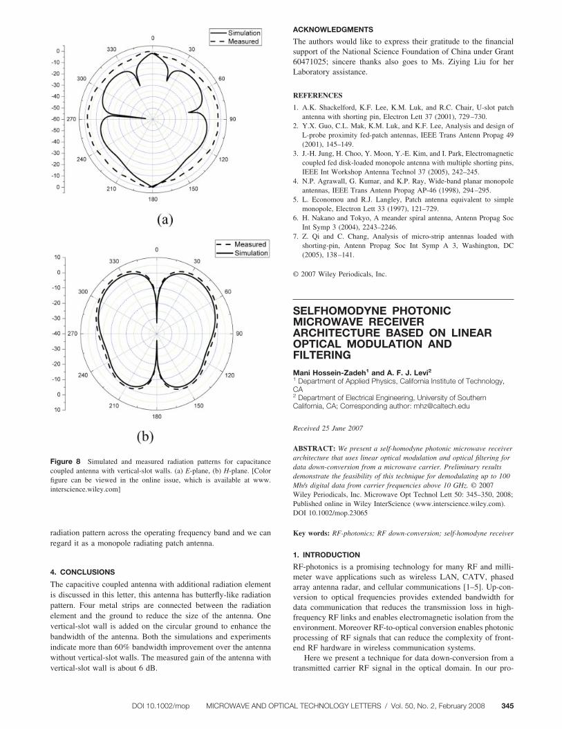
At the same, the simulated and measured E-plane and H-planeradiation patterns at frequency 3 GHz are shown as the solid linesand dotted lines in Figures 8(a) and 8(b), respectively. It can beseen that capacitive coupled antenna has butterfly-like E-planeradiation pattern. The simulated and measured gains of the capac-itive coupled antenna with vertical slots sidewalls ground are 4.64dB and 6.0 dB, respectively. We may note that there are someripples in the H-plane, probably owing to the fabrication inaccu-racy. However, the ripple levels are quite low within the tolerablerange. Obviously, this antenna has nearly omnidirectional H-plane
Figure 5 Simulated and measured radiation patterns for capacitancecoupled antenna without vertical-slot walls. (a) E-plane, (b) H-plane.[Color figure can be viewed in the online issue, which is available atwww.interscience.wiley.com]
Figure 6 The prototype of the capacitive coupled antenna with vertical-slot walls. [Color figure can be viewed in the online issue, which isavailable at www.interscience.wiley.com]
Figure 7 Simulated and measured return loss of the capacitive coupledantenna with vertical-slot walls
344 MICROWAVE AND OPTICAL TECHNOLOGY LETTERS / Vol. 50, No. 2, February 2008 DOI 10.1002/mop
radiation pattern across the operating frequency band and we canregard it as a monopole radiating patch antenna.
4. CONCLUSIONS
The capacitive coupled antenna with additional radiation elementis discussed in this letter, this antenna has butterfly-like radiationpattern. Four metal strips are connected between the radiationelement and the ground to reduce the size of the antenna. Onevertical-slot wall is added on the circular ground to enhance thebandwidth of the antenna. Both the simulations and experimentsindicate more than 60% bandwidth improvement over the antennawithout vertical-slot walls. The measured gain of the antenna withvertical-slot wall is about 6 dB.
ACKNOWLEDGMENTS
The authors would like to express their gratitude to the financialsupport of the National Science Foundation of China under Grant60471025; sincere thanks also goes to Ms. Ziying Liu for herLaboratory assistance.
REFERENCES
1. A.K. Shackelford, K.F. Lee, K.M. Luk, and R.C. Chair, U-slot patchantenna with shorting pin, Electron Lett 37 (2001), 729–730.
2. Y.X. Guo, C.L. Mak, K.M. Luk, and K.F. Lee, Analysis and design ofL-probe proximity fed-patch antennas, IEEE Trans Antenn Propag 49(2001), 145–149.
3. J.-H. Jung, H. Choo, Y. Moon, Y.-E. Kim, and I. Park, Electromagneticcoupled fed disk-loaded monopole antenna with multiple shorting pins,IEEE Int Workshop Antenna Technol 37 (2005), 242–245.
4. N.P. Agrawall, G. Kumar, and K.P. Ray, Wide-band planar monopoleantennas, IEEE Trans Antenn Propag AP-46 (1998), 294–295.
5. L. Economou and R.J. Langley, Patch antenna equivalent to simplemonopole, Electron Lett 33 (1997), 121–729.
6. H. Nakano and Tokyo, A meander spiral antenna, Antenn Propag SocInt Symp 3 (2004), 2243–2246.
7. Z. Qi and C. Chang, Analysis of micro-strip antennas loaded withshorting-pin, Antenn Propag Soc Int Symp A 3, Washington, DC(2005), 138–141.
© 2007 Wiley Periodicals, Inc.
SELFHOMODYNE PHOTONICMICROWAVE RECEIVERARCHITECTURE BASED ON LINEAROPTICAL MODULATION ANDFILTERING
Mani Hossein-Zadeh1 and A. F. J. Levi21 Department of Applied Physics, California Institute of Technology,CA2 Department of Electrical Engineering, University of SouthernCalifornia, CA; Corresponding author: [email protected]
Received 25 June 2007
ABSTRACT: We present a self-homodyne photonic microwave receiverarchitecture that uses linear optical modulation and optical filtering fordata down-conversion from a microwave carrier. Preliminary resultsdemonstrate the feasibility of this technique for demodulating up to 100Mb/s digital data from carrier frequencies above 10 GHz. © 2007Wiley Periodicals, Inc. Microwave Opt Technol Lett 50: 345–350, 2008;Published online in Wiley InterScience (www.interscience.wiley.com).DOI 10.1002/mop.23065
Key words: RF-photonics; RF down-conversion; self-homodyne receiver
1. INTRODUCTION
RF-photonics is a promising technology for many RF and milli-meter wave applications such as wireless LAN, CATV, phasedarray antenna radar, and cellular communications [1–5]. Up-con-version to optical frequencies provides extended bandwidth fordata communication that reduces the transmission loss in high-frequency RF links and enables electromagnetic isolation from theenvironment. Moreover RF-to-optical conversion enables photonicprocessing of RF signals that can reduce the complexity of front-end RF hardware in wireless communication systems.
Here we present a technique for data down-conversion from atransmitted carrier RF signal in the optical domain. In our pro-
Figure 8 Simulated and measured radiation patterns for capacitancecoupled antenna with vertical-slot walls. (a) E-plane, (b) H-plane. [Colorfigure can be viewed in the online issue, which is available at www.interscience.wiley.com]
DOI 10.1002/mop MICROWAVE AND OPTICAL TECHNOLOGY LETTERS / Vol. 50, No. 2, February 2008 345