Embed Size (px)
Citation preview

Bandpass filtering of high-speed forwarded clocks
Timothy M. Hollis Æ David J. Comer
Received: 12 March 2007 / Revised: 29 January 2008 / Accepted: 29 January 2008 / Published online: 20 February 2008
� Springer Science+Business Media, LLC 2008
Abstract Bandpass channel filtering is shown to attenu-
ate both random and determinstic jitter components in high
frequency clock signals. A fully differential, tunable LC
bandpass filter is developed and employed to reduce
Gaussian and sinusoidal distributed jitter and duty cycle
distortion.
Keywords Clock jitter � Duty cycle distortion �Bandpass filters
1 Introduction
It was not long after its initial introduction that digital
communication was recognized as being superior to its
analog counterpart in several respects, the most important
of which was its inherent immunity to noise. Consequently,
the principles of digital communication were quickly
adopted into existing communication media wherever
possible. While the majority of present day baseband
communication systems are still theoretically digital, the
signals being transmitted have become more analog in
nature as datarates approach and exceed the physical
bandwidth of the transmission path. High-speed chip-
to-chip interconnects, in particular, are severely impeded
by the physical characteristics of the commodity printed
circuit board channel.
As chip-to-chip communication returns to the analog
domain, so returns the struggle to cope with and overcome
noise. Whether it is random thermal noise or deterministic
noise resulting from asymmetries, discontinuities, and/or
band limitations associated with the signal path, voltage
noise present in clock and data waveforms is converted to
timing noise or jitter at each signal transition. As a result,
timing margins are not only reduced by the diminishing
symbol period associated with high frequency transmis-
sion, but also by timing uncertainties which tend to grow
with signaling frequency. As that jitter increases, so does
the probability of incorrectly interpreting the transmitted
data. Thus, the ability to suppress noise and jitter is
essential in high-speed communication systems.
Perhaps the most popular high-speed interconnect today
is the source-synchronous topology (see Fig. 1), in which
both the data and an associated clock are forwarded in
parallel from one chip to the next. By carefully matching
the clock and data paths, system and environmental noise
tend to impact both signals equivalently. When the for-
warded clock is then used to capture the data in the
receiver, any correlated clock and data signal noise theo-
retically cancels. At higher datarates, however, it becomes
difficult to guarantee matching between the clock and data
paths, and as a result many high performance designs are
migrating to topologies wherein the chip-to-chip intercon-
nect is no longer strictly source-synchronous. Such
schemes typically compensate for clock-to-data mismatch
by introducing re-timing circuits (e.g. phase-locked loops,
etc.) into the clock path.
Over the years, data channel signal integrity has enjoyed
a disproportionally greater degree of attention, as the data
signal’s broadband nature makes it inherently more sus-
ceptible to degradation associated with limited channel
bandwidth. Clock signal integrity, on the other hand, has
received relatively little attention, as the clock’s periodic
nature side-steps pattern dependent degradation, and as a
result, clock quality or lack thereof has contributed
T. M. Hollis (&) � D. J. Comer
Brigham Young University, 459 Clyde Building, Provo, UT
84602, USA
e-mail: [email protected]
123
Analog Integr Circ Sig Process (2008) 54:171–186
DOI 10.1007/s10470-008-9145-1

relatively little to input/output (I/O) performance limitation
in the past. At multi-Gigabit/second (Gb/s) datarates,
however, new phenomena including jitter amplification, in
conjunction with stricter timing budgets to cope with
vanishing margins, have raised interest in clock signal
integrity.
As the clock finds use at more and more nodes within
the system, as is the case with the source-synchronous and
other forwarded-clock topologies, the impact of clock
signal integrity on link performance becomes more serious,
as uncertainty in the timing of the clock, or clock jitter,
rapidly degrades the maximum achievable datarate. When
targeting multi-Gb/s communication, it is reasonable to
expect the total clock jitter observed at the point of data
capture to contain some, if not all, of the following com-
ponents: jitter generated within a phase-locked loop (PLL)
used during the transmit-side serialization process; jitter
generated by the transmit drivers, the majority of which
stems from simultaneous switching output (SSO) noise;
jitter induced through inductive and capacitive crosstalk;
jitter amplification imposed by the band-limited charac-
teristics of the transmission channel; jitter generation
within the receive-side clock buffer, including duty cycle
distortion (DCD) resulting from non-ideal DC signal levels
at the input buffer; jitter resulting from clock multiplication
or phase interpolation circuits used to realign the phase of
the associated clock and data signals; jitter induced by
power and ground noise at either end of the link; and finally
jitter amplification incurred through the clock distribution
network. While any jitter common to both clock and data
signals will cancel during the data capture operation,
uncorrelated clock-to-data jitter directly degrades the data
capture process.
This work targets jitter reduction in forwarded-clock
signals through bandpass filtering. While the use of band-
pass filters to reduce noise has been practiced in RF and
optical communication systems for decades, such an
approach has yet to be implemented in a standard CMOS-
based chip-to-chip communication link for the specific
purpose of limiting forwarded-clock timing jitter.
To justify this work, the sections that follow present a
review of the various jitter components observed in high
frequency clock signals, and the way those components
respond to the band limitations associated with multi-Gb/s
communication. Within each section will be a qualitative
or quantitive argument for the use of bandpass filtering to
address the jitter component under consideration. This will
be followed by a discussion of how clock and data signal
jitter combine to limit performance in high-speed source-
synchronous interconnects, steering the design of the sig-
naling topology. Finally, a fully differential, tunable LC
(inductor-capacitor based) bandpass filter will be presented
and shown not only to reduce jitter-producing voltage
noise, but also to effectively suppress several forms of
existing jitter encountered in periodic waveforms.
Before proceeding, however, we provide an intuitive
argument for the use of bandpass filters in high-speed clock
signal conditioning. Figure 2 presents the spectral com-
ponents of an ideal clock waveform, with fundamental
frequency fc, along with the corresponding spectral char-
acteristics of several forms of signal degradation. The
frequency response of a bandpass filter is superimposed for
the sake of the discussion. The first thing to notice are the
arrows pointed up and down at each harmonic component
of the clock, representing harmonic distortion, which often
includes DCD. Thermal noise, power supply noise, cross-
talk, and inter-symbol interference (ISI) are also overlaid,
though admittedly the noise levels are not to scale.
Regardless, by identifying the spectral characteristics of the
various noise sources with respect to the bandpass enve-
lope, it becomes clear that sifting the dominant component
of the signal through a bandpass filter will suppress noise
occuring beyond the filter’s bandwidth. How well this
concept is realized through circuit design, and how effec-
tive it is in reducing timing jitter is the emphasis of this
work.
TransmitterSerialization
andSynchronization
ReceiverSampling
andDe-serialization
Data Channel
Clock Channel
ParallelData
ParallelData
Source-Synchronous Clock
Fig. 1 A simplified source-synchronous link illustrating the relation-
ship between the forwarded-clock and the data throughout the
interconnect system
Device and Component Noise
Power Supply Noise
Harmonic Distortion (DCD)
Crosstalk and ISI
Frequency
Bandpass Envelope
fc
Fig. 2 High-level frequency domain illustration of the impact that a
bandpass filter should have on the spectral components of clock
degrading noise
172 Analog Integr Circ Sig Process (2008) 54:171–186
123

2 Characteristics of clock jitter
The first step in the process of overcoming a design chal-
lenge is to gain a comprehensive understanding of the
nature of the problem. Figure 3 presents a two-cycle eye
diagram of 4 Gb/s data following transmission across four
inches of FR4 printed circuit board material and illustrates
the threat jitter poses to the signal integrity of high-speed
interconnects. To identify the synergistic relationship of
clock and data jitter, the rising and falling edges of the
corresponding sampling clock are overlaid. With the signal
concentration accounted for by the shade of the waveform
(higher concentration = lighter shading) it is possible to
visualize, albeit crudely, the distribution of the signals in
both the voltage and time dimensions. Even without the
signal shading, it is clear that the timing uncertainty of the
data signal is significantly greater than that of the clock. In
this particular case, and in general, the data timing varia-
tion is dominated by pattern or data-dependent jitter (DDJ)
stemming from ISI, a phenomenon attributed to the band
limitation of the channel.
While the clock passes over and is reshaped by a similar
if not identical channel, its periodicity is not affected by the
high frequency channel losses in the same way that the
timing of the random data signals is. In the figure, the clock
waveform also appears different as it corresponds to the
buffered rail-to-rail output of a complicated clock distri-
bution network used to minimize the skew between the
clock’s arrival at the various data inputs along the incom-
ing data bus, and represents the anticipated clock integrity
at the point of data capture. Due to the growing cost of pins
on the integrated circuit package, a single clock is often
associated with 8–32 data lanes. When this occurs, the
clock must be distributed across the receiver, introducing
latency and potentially de-correlating noise and jitter that
were common to the clock and data signals at the pad.
It can be demonstrated from the figure that while clock
jitter directly reduces the timing margin, it also indirectly
reduces the voltage margin. For example, as the sampling
uncertainty or clock jitter increases, data sampling may
occur further and further from the horizontal center of the
eye. From the figure it is clear that when the rounded data
eye is sampled near the transitions, the value sampled over
that region in time will have less amplitude with respect to
the reference voltage (Vref), and hence less voltage mar-
gin. Thus the growing concern over clock integrity is
appropriate, and in order to most efficiently address these
issues, it is necessary to distinguish between the charac-
teristics of the various clock jitter components.
2.1 Random jitter
Unbounded random jitter, which is often assumed to
exhibit a Gaussian probability distribution and is conse-
quently quantified with an rms value, is typically associated
with random perturbations in the signal amplitude. Such
variations in amplitude occuring at or near signal transi-
tions lead to a corresponding variation in the Vref crossing
time of the signal, due to finite signal risetime and falltime.
As illustrated in Fig. 4, this translation of voltage noise to
jitter is inversely proportional to the signal slew-rate, which
fact gives rise to an important trade-off in the signaling
design: higher slew-rates limit random noise-to-jitter
translation, but slower slew-rates tend to minimize induc-
tive effects such as ringing in the signal, thereby reducing
the signal noise amplitude. Un-predictable power supply
noise and electromagnetic effects also bleed through to the
signal, resulting in what appears to be a second random
jitter component, yet because this contribution is often
bounded, a distinction is made by refering to it as uncor-
related-bounded jitter.
Based on this principle of noise-to-jitter translation, one
seemingly obvious method for minimizing random jitter is
to minimize the random noise. The best known, andData Jitter Clock Jitter
Signal Noise
Vref
Data Signal
Clocks Signal
Vref Noise+
ReceiverSensitivity
Fig. 3 Illustration of the combined impact of data and clock jitter on
timing margin
Vo
ltag
eD
istr
ibu
tio
n
Timing Distribution
Vo
ltag
eD
istr
ibu
tio
n
Timing Distribution
Fast Edge Slow Edge
Fig. 4 Illustration of the translation of random noise to random jitter
through the slew-rate of the associated signal
Analog Integr Circ Sig Process (2008) 54:171–186 173
123

according to communication theory the optimal, approach
for addressing random voltage noise is the Wiener Filter, as
it identifies the frequency content of the signal and in turn
only provides amplification at those frequencies, thus
avoiding the amplification of noise while increasing the
signal-to-noise ratio (SNR). But as the implementation of
the optimal Wiener Filter may be prohibitively complex,
more practical approximations have been developed. In
addition to the improvement realized by the Kalman Filter,
which approximates the Wiener Filter through iterative
adaptation of the filter coefficients, perhaps the most
widely accepted method for addressing and reducing ran-
dom noise components, or conversely increasing the SNR,
is through matched filtering, in which the impulse response
of the filter is the time reversed, delayed conjugate of the
transmitted pulse. Mathematically it can be shown that the
convolution of the transmitted symbol with the impulse
response of the matched filter optimizes the SNR for the
case of random noise, uncorrelated to the signal [1, 2].
If the matched filter is thought of as a sub-optimal
Wiener Filter, then a bandpass filter may be considered a
sub-optimal ‘‘match‘‘ to a clock signal. When the bandpass
filter’s center frequency is tuned to the fundamental or
dominant clock harmonic, then it also only amplifies over
the spectral region containing the majority of the signal
energy. The sub-optimality is the bandpass filter’s failure to
simultaneously amplify the odd harmonics of the clock,
which would more closely approximate the Wiener Filter.
A more quantitative argument for bandpass filtering
requires some discussion of jitter amplification. Jitter
amplification corresponds to the system’s response to a unit
jitter impulse, perhaps simulated by a single edge timing
deviation within an otherwise ideal periodic signal. The
number of trailing cycles required for the edge timing to re-
settle to the ideal is a distinct characteristic of the system.
The jitter impulse response is found by measuring the
difference between the ideal edge timing and the timing
due to the perturbation, and from that value a jitter transfer
function may be calculated. In addition, once the jitter
impulse response is acquired, a jitter amplification factor
may be computed through the expression
JAmp ¼ffiffiffiffiffiffiffiffiffiffiffiffiffiffiffiffiffi
X
i
JIR2i
r
; ð1Þ
where JIRi are the sampled values of the jitter impulse
response between the initial occurence of the perturbation
and the final edge settling time. The jitter amplification
factor then serves as a scaling term by which the known
rms input jitter may be multiplied to compute the expected
rms output jitter.
For the measured channel response shown in Fig. 5,
corresponding to a six inch copper trace in an FR4-based
printed circuit board (the target channel for this work), the
associated random jitter and DCD amplification factors are
presented versus clock frequency in Fig. 6.
These figures identify some important characteristics of
high frequency clock transmission. From Fig. 6 it is
observed that random jitter amplification tends to increase
with operating frequency, and thus the frequency of the
forwarded-clock should not be chosen lightly. In the
20 Gb/s link presented in [3], two of the major factors
driving the choice of clock frequency were the channel
loss at the frequencies under consideration and the jitter
amplification at those frequencies. Based on data like that
found in Figs. 5 and 6, a 1/4-rate clock (5 GHz) was
chosen rather than the more commonly employed 1/2-rate
Fig. 5 Target clock channel frequency response for a six inch
channel across an FR4-based printed circuit board
Fig. 6 Anticipated random jitter and DCD amplification at various
clock frequencies for a six inch channel across an FR4-based printed
circuit board
174 Analog Integr Circ Sig Process (2008) 54:171–186
123

clock. Not only did this decision avoid the additional
10.5 dB of loss predicted at 10 GHz, but it also avoided a
random jitter amplification of nearly 29, versus the jitter
amplification anticipated at 5 GHz of just over 19.
In a similar way, jitter amplification factors for two
different bandpass filter configurations are presented in
Fig. 7. Here again, the clock frequency is swept, while the
two filters maintain a fixed center frequency of 5 GHz, but
distinct quality (Q) factors of 2.5 and 5. Based on this
figure, it is expected that bandpass filtering will actually
reduce the rms jitter present in a signal, due to its jitter
amplification factor being less than one at a clock fre-
quency of 5 GHz. The figure also demonstrates that the
jitter suppression provided by bandpass filtering improves
with the filter Q, supporting a previous claim that bandpass
filters may reduce cyclic phase noise and jitter by a factor
of p2Q [4].
A final observation based on these last three figures is
that even a relatively low-Q filter may not only counter the
jitter amplification experienced across the channel, but may
even reduce the jitter below its initial level, as will be
demonstrated here. When the frequency response of the
channel shown in Fig. 5 is followed by the response of
the relatively low-Q bandpass filter to be presented shortly,
the result is a combined jitter amplification of approxi-
mately 0.5, or the product of the channel and subsequent
filter jitter amplification factors.
2.2 Duty cycle distortion
DCD, the second jitter component considered, results from
duty cycle error; when the ratio of the signal pulse width to
the period deviates from 1/2 due to DC offsets in the signal,
rise/fall time discrepancies, device mismatch in the signal
path or any combination of the three. Inequalities between
the pulse and space widths of clock signals are particularly
troublesome in double-data rate (DDR) systems, where the
data stream is sampled with both the rising and falling
edges of the clock. A portion of the analysis that follows
was first presented by the authors in [5].
DCD falls in the category of deterministic or periodic
jitter, allowing it to be quantified with a peak-to-peak
value. When combined with random, Gaussian distributed
jitter, DCD produces a bimodal jitter distribution, as
illustrated in Fig. 8. While the ideal sampling instant (clock
edge) should occur at the center of the data eye, the pres-
ence of DCD results in the concentration of clock edges
around a pair of timing instants, with the distance between
the bimodal peaks corresponding to the peak-to-peak DCD.
Thus, the contribution of DCD to the spreading of the
sampling distribution, and subsequent timing and voltage
margin degradation, is significant.
Attenuation of DCD present in clock signals can be
approached in two ways: attacking the source of the jitter
(duty cycle error) and/or attacking the resulting jitter itself.
Application of these two approaches may be separated into
distinct operations on the low and high frequency compo-
nents of the signal.
2.2.1 Low frequency conditioning
Low frequency conditioning refers to the removal of
unwanted DC offset from the signal. One of the effects of
Fig. 7 Anticipated random jitter and DCD amplification for two
bandpass filters with Qs of 2.5 and 5
Vref
Duty Cycle Distortion Sampling Clock Jitter
DataJitter
DataJitter
Data
Clock
Fig. 8 Eye diagram illustrating the effects of both clock and data
jitter on timing margin. Duty cycle distortion produces the bimodal
sampling clock distribution
Analog Integr Circ Sig Process (2008) 54:171–186 175
123

the lowpass channel is to degrade the rising and falling
signal transitions. The exaggerated rising and falling tran-
sitions shown in Fig. 9 help to demonstrate the dependence
of duty cycle on DC offsets. The signal shown is nothing
more than a symmetric square wave that has been shifted in
the positive vertical direction by a small amount. That
small shift, in conjunction with the finite slopes of the
transitions, produces a shift in the reference voltage
crossing times of the signal, and hence, duty cycle error.
For the reference voltage shown, the duty cycle (sPulse/
(sPulse + sSpace)) is clearly greater than 50%. And while the
presence of DC offset is not the only source of duty cycle
error, an unwanted DC component tends to accumulate as a
result of DCD, regardless of the source of the error, as
illustrated in Fig. 10, which demonstrates the effect of
lowpass channels on clock signals with duty cycle greater
than 50%.
With regard to the diagram, the mismatch between the
positive and negative pulses results in a non-zero DC or
average value due to the integrating nature of the channel
(i.e. the area under the pulses do not cancel completely).
Then, in accordance with the previous discussion sur-
rounding Fig. 9, DCD will grow due to the increased
offset. Thus, a cycle is born wherein DCD leads to
increasing signal offset, and signal offset leads to increased
DCD, which suggests that the suppression of low frequency
signal components, or at least the DC component, should
aid in the attenuation of DCD.
2.2.2 High frequency conditioning
The high frequency nature of DCD can best be understood
through Fourier analysis. A simple Fourier series, which
models a clock with controllable levels of DCD, may be
derived as follows:
1. The waveform shown in Fig. 11 represents a clock
signal which alternates between values of zero and one
with period T. By including the variables sr and sf at
the transitions it is possible to simulate the existence of
duty cycle error through the manipulation of the rising
and falling edges of the pulse as follows:
Positive sr shifts the rising edge left (early),
Negative sr shifts the rising edge right (delay),
Positive sf shifts the falling edge left (early), and
Negative sf shifts the falling edge right (delay).
2. The expression into which the Fourier coefficients will
be inserted is
CðtÞ ¼ A0 þX
1
n¼1
An cos2npT
t
� �
þ Bn sin2npT
t
� �
;
where C(t) = the resulting clock signal, t = the timing
instant, T = the signal period, and n = the integer multiple
frequency (harmonic).
3. The A0 term represents the DC or average value of the
waveform, and is found by evaluating the integral
A0 ¼1
T
Z T4�sf
�T4�sr
dx: ð2Þ
4. The An and Bn terms are similarly found by evaluating
the folowing integrals
An ¼2
T
Z T4�sf
�T4�sr
cos2npT
x
� �
dx ð3Þ
and
Bn ¼2
T
Z T4�sf
�T4�sr
sin2npT
x
� �
dx: ð4Þ
5. The resulting coefficient values are
A0 ¼1
21þ 2ðsr � sf Þ
T
� �
; ð5Þ
Pulse Pulse
Spacee
Vref
Fig. 9 Illustration of how the addition of any amount of DC offset
voltage to a perfectly symmetric, finite rise/fall time, square wave
generates duty cycle error
1
0
-1
t
Fig. 10 Illustration of how DCD in a signal accumulates across a
lowpass channel
176 Analog Integr Circ Sig Process (2008) 54:171–186
123

An ¼1
npsin
2npT
T
4þ sf
� �� �
� sin2npT
sr �T
4
� �� �� �
;
ð6Þ
and
Bn ¼1
npcos
2npT
sr �T
4
� �� �
� cos2npT
T
4þ sf
� �� �� �
ð7Þ
Figure 12 illustrates the effects of duty cycle error on
the high frequency components of the clock signal. A
10 GHz clock signal, generated by the Fourier series just
discussed, is shown in the upper window. The falling edge
is delayed, in one case, by 25 ps to compare an ideal clock
with one exhibiting DCD. The lower window shows the
resulting shift in the magnitude of the first ten harmonic
components. As these harmonics represent integer multiple
frequencies of the fundamental, it can be understood that
DCD manifests itself at frequencies equal to and above the
fundamental frequency of the signal. An additional point of
interest is the fact that the even harmonics, which do not
exist in the ideal signal, take on nonzero values as the duty
cycle error increases, with the second harmonic appearing
to be the dominant DCD component.
It should be clear from the figure that suppression of
DCD requires the blocking of frequencies equal to and
greater than the second harmonic of the clock signal. This
implies that the common remedy of countering high fre-
quency channel losses through highpass equalization not
only fails to target DCD, but in fact tends to amplify this
jitter component by amplifying the distorted higher order
harmonics of the signal.
A more appropriate filter would be capable of simulta-
neously amplifying the fundamental clock frequency while
filtering off the corresponding harmonic components. This
could be accomplished with inductive peaking (high-Q,
low-pass filtering) at the clock fundamental frequency, yet
this would still fail to completely suppress the DC com-
ponent of the signal, and therefore would sacrifice some
potential attenuation of the duty cycle error as discussed
previously. On the other hand, the inherent ability of a
bandpass filter to amplify a narrow band of the signal’s
frequency spectrum, while completely removing the DC
and unwanted higher order harmonic components, makes
this filter an attractive candidate in the effort to mitigate
DCD.
2.3 Periodic and sinusoidal jitter
While DCD has been shown to exhibit periodicity at fre-
quencies 29 and above the clock fundamental, other lower
frequency periodic jitter components are often observed in
high-speed clock signals as well. For example, spread-
spectrum clocking, which is simply a low frequency
modulation of the transmitted clock phase used to reduce
electomagnetic emissions, is manifested in the time domain
as a low frequency periodic jitter. For the most part, this
particular jitter component is rarely a problem in that the
modulated clock signal is used as the trigger for data
serialization and transmission and cancels out during data
capture at the receiving end. Even though the peak mag-
nitude of the spread-spectrum clock jitter is specified in
nanoseconds and may span several cycles, its slow oscil-
lation (&33 kHz) provides tolerance to clock-data path
mismatch. On the other hand, periodic jitter components at
higher frequencies, stemming from PLL jitter peaking or
the excitation of integrated circuit package resonant fre-
quencies, may be less tolerant to skew and must be
addressed.
-T/4 +T/2-T/2 +T/40
+τr +τf
0
1
-τr -τf
Fig. 11 Waveform used in the derivation of the Fourier series
representing a clock with DCD
Fig. 12 The upper window presents an ideal clock waveform
compared with a clock exhibiting 25 ps of DCD by delaying the
falling edge of the second waveform through the paramterized Fourier
series just derived. The lower window presents the resulting variation
in the 10 GHz fundamental and the first nine higher order harmonics,
illustrating the high frequency nature of jitter due to duty cycle error
Analog Integr Circ Sig Process (2008) 54:171–186 177
123

To understand the bandpass filter’s impact on periodic
jitter, it is helpful to refer to the long-held approximation that
‘‘it takes Q cycles for a circuit to respond to changes at its
input.‘‘ Thus if a jitter event appears at the input of a high-Q
filter, but is reversed within Q cycles, then the perturbation
should not be observed at the circuit output. This would
imply that clock jitter at frequencies above fc/Q will be
attenuated or possibly completely eliminated by a bandpass
filter centered over the clock’s fundamental frequency. In
other words, the slow response of the filter tends to average
out high frequency timing perturbations, much the way a
matched filter improves SNR through integrating the noise
over time. The high frequency periodic jitter attenuation
provided by the bandpass filter may further be compared to
the reduced jitter transfer above the loop filter cutoff fre-
quency of PLLs, as will be discussed in a later section.
To verify periodic jitter attenuation, a sinudoial jitter
component with a peak-to-peak magnitude of 20 ps was
superimposed onto a 5 GHz clock and passed through the
bandpass filter presented in a later section, while sweeping
the jitter frequency from 100 MHz to 10 GHz. Figure 13
shows the results, with the simulated jitter amplification of
the filter respresented by the ‘‘*’’ symbols. Due to numerical
issues the simulation produced several spikes depending on
the phase relationship of the jitter and the underlying clock
signal. To improve the readability of the data, best-fit curves
are included. From the solid black line it appears that
sinusoidal jitter amplification is symmetric about the clock
frequency. We suggest that this is due to the frequency
relationship of the oscillating jitter and the underlying
clock, which modulates the edge timing according to the
ratio of the two frequencies. When the clock and oscillating
jitter frequencies are equal, the magnitude of the jitter will
be the same at each clock edge and therefore will appear as
a static phase shift or zero cycle-to-cycle jitter. Because the
same jitter-to-clock frequency ratio exists at the output of
the filter, the same static phase shift is observed in the
output signal and the corresponding jitter amplification
(jitterout/jitterin) equals unity. This does not imply that jitter
amplification is worse at the bandpass filter’s center fre-
quency, but that the input jitter, and consequently the output
jitter are both minimized at that point.
At the relative frequencies of 1/2fc and 3/2fc, the filter
reduces the peak sinusoidal jitter amplitude by as much as
40%, which is close to the value predicted in [3] of p2Q ; or
0.5991 for this particular circuit implementation. It is actu-
ally possible to find frequencies at which the filter suppresses
the sinusoidal jitter magnitude even further, as will be
demonstrated near the conclusion of this presentation.
To further verify that the simulated results were not
purely a numerical phenomenon, the simulation was
repeated using the six inch channel response shown in
Fig. 5, in place of the bandpass filter response. The data
from this simulation is also included in Fig. 13 represented
by the ‘‘o‘‘ symbols and the corresponding best-fit curve.
Clearly the lowpass channel has a consistently negative
impact on the magnitude of the sinusoidal jitter, regardless
of frequency, though it does exhibit a similar symmetry.
From these observations, it is clear that bandpass filters
reduce unwanted periodic jitter over a range of frequencies,
over which other filtering operations are likely to amplify
the peak-to-peak jitter.
3 Existing solutions for reducing clock jitter
As was mentioned previously, PLLs are often employed
within receivers to realign clock and data signals at the
point of data capture and compensate for clock-data chip-
to-chip routing mismatch and latency introduced by clock
distribution networks. PLLs also commonly find their place
in Process, Voltage and Temperature (PVT) compensation
circuitry. One of the potentially positive side effects of
incorporating a PLL into the clock path is that when
designed correctly the clock signal leaving the PLL may
exhibit less high frequency jitter than the clock signal that
was originally fed into the circuit.
This potential for high frequency jitter attenuation is
associated with the PLL’s phase tracking capability. One of
the major considerations of the PLL design is the band-
width of the control loop, which defines the frequency
range over which changes in the input signal phase may be
tracked by the circuit. Physically, the tracking bandwidth
of the PLL is set by the cutoff frequency of an internal
lowpass filter. Transition timing or phase variation at the
PLL’s input falling above the cutoff frequency of the loop
Fig. 13 Sinusoidal jitter amplification of the proposed bandpass filter
with clock frequency fixed at 5 GHz and sinusoidal jitter frequency
swept from 100 MHz to 10 GHz
178 Analog Integr Circ Sig Process (2008) 54:171–186
123

filter are not trackable, and from the perspective of the
tracking mechanism, high frequency jitter is no different.
Thus timing jitter beyond the bandwidth of the system is
filtered off resulting in a lowpass jitter transfer character-
istic from PLL input to output.
Unfortunately, jitter from the input signal is not the only
component of timing error that may pass to the output of
the PLL. Power supply noise and voltage controlled
oscillator (VCO) phase noise both contribute to the total
output jitter after being shaped by the jitter transfer char-
acteristics of the system. According to [6], the jitter transfer
of VCO phase noise through the output buffer is highpass
in nature, while jitter stemming from the power supply
sensitivity of the output buffer itself is bandpassed by the
combination of lowpass and highpass functions associated
with the loop filter and the output buffer, respectively [6].
Additionally, the phase detector, charge pump, and any
frequency division circuitry will also contribute to the jitter
reaching the PLL output. Thus it is possible for the PLL
output to exhibit more jitter than the input, despite the
input/output (I/O) jitter filtering of the control loop. While
several techniques to reduce the jitter generated from
within the PLL have been studied, including a recently
published work in which injection locking the reference
clock to a slave oscillator was proposed and shown effec-
tive [7], most new methods under consideration add
complexity to an already complicated circuit.
In addition to the possibility of contributing more jitter
to the system than it removes, the very filtering nature of
the PLL could prove detrimental to the communication
system. For even though the jitter suppressing behavior of
PLLs is often deemed essential, a case may easily be
derived in which the jitter transfer characteristics of the
PLL actually degrade the performance of the overall
interconnect. For example if both the clock and data signals
contain periodic jitter components, such as spread spectrum
clocking or deterministic jitter resulting from the excitation
of certain modes in the package resonance, then it would be
critical to maintain the correlation between those compo-
nents in both signals.
To apply numbers to this qualitative explanation, sup-
pose both clock and data signals are transmitted exhibiting
periodic jitter components at 500 kHz and 50 MHz. If the
clock signal passes through a PLL with a loop bandwidth
of 25 MHz then the 50 MHz jitter on the clock will be
filtered away and no longer correlated to the corresponding
component of the data jitter. In addition, it is possible that
the PLL will introduce new periodic components and cer-
tainly additional random jitter around the loop filter cutoff
frequency due to a phenomenon known as jitter peaking.
Thus it is reasonable to assume that the PLL will not only
remove the 50 MHz jitter needed to match the data path,
but it may also introduce jitter near 25 MHz that has no
correlation to the data jitter, further degrading the perfor-
mance sought through careful routing in the first place. In
this particular case, the system performance may be
improved by avoiding the inclusion of the PLL.
More often, the PLL designer must address the trade-off
between filtering input signal jitter and tracking deter-
ministic jitter components in the signal, through the
selection of the loop bandwidth. If the loop bandwidth in
the previous example was raised above 50 MHz to track
the anticipated jitter component at that frequency, then
additional random jitter between the original 25 MHz loop
bandwidth and the current 50 MHz bandwidth would
consequently pass to the output as well. In [3], the solution
was to increase the loop bandwidth to 500 MHz to facili-
tate better jitter tracking, while at the same time taking
other steps to compensate for the increased jitter passed by
the high bandwidth PLL.
When maintaining jitter correlation between the clock
and data signals is more important, a better solution may be
to replace the PLL with a delay-locked loop (DLL), whose
jitter transfer characteristics are very different. It is well
known, and at times considered a negative characteristic,
that DLLs pass jitter from input to output without attenu-
ation. The jitter passing behavior of DLLs occurs because
the waveform at the output is simply a delayed version of
the input rather than a signal generated from within the
system, as is the case with the VCO output of the PLL. In
cases like that described above, such an allpass type of
jitter transfer might be advantageous, as it maintains more
of the clock-to-data jitter correlation while still providing
for phase alignment and timing compensation.
To counter the increased random signal jitter which
results with the DLL, a bandpass filter may be incorporated
into the signal path to provide jitter filtering above fc/Q,
where fc is the center frequency of the filter, and ideally the
frequency of the clock’s fundamental component. This
technique passes the lower frequency sinusoidal jitter,
while reducing the high frequency jitter that has no cor-
related component in the data signal. The trade-off is that
random jitter at frequencies between the alternative PLL
bandwidth and fc/Q will pass, though the noise filtering
characteristics of the filter should provide additional benefit
not accounted for in this discussion.
4 Design of the clock filter
The design of a high frequency bandpass filter in standard
CMOS requires several degrees of consideration. At the
highest level, the trade-offs between digital and analog
filter topologies are compared. In this case, the target center
frequency of 5 GHz precludes the use of strictly digital
techniques, due to the required circuit bandwidth. Even
Analog Integr Circ Sig Process (2008) 54:171–186 179
123

within the analog domain, the decision between discrete-
time and continuous-time architectures must be made. While
discrete-time filters are routinely used at high frequency, for
this implementation they are less attractive based on the large
number of taps required to realize the filter response and the
high level of noise expected from discrete-time implemen-
tation. At the next level, active versus passive filtering is
considered. Based on the anticipated channel loss at 5 GHz
(the target clock frequency), providing some gain within the
circuit is desirable and implies that active filtering will be
superior. The decision to achieve the filter frequency
response through an LC-tank resulted from the need to
minimize jitter generation from within the filter itself.
Figure 14 presents the proposed fully differential, LC
bandpass filter and corresponding component values are
listed in Table 1. Prior to adding the input AC coupling,
formed by components RC1, RC2, CC1, and CC2, the cor-
responding filter transfer function is
FðsÞ ¼Cgd
CgdþCLsþ Rs
L
� �
s� gm
Cgd
�
s2 þ Rs
L þ 1rdsðCgdþCLÞ
�
sþ 1LðCgdþCLÞ
; ð8Þ
where L, Rs, gm, Cgd, and CL are the inductance, the par-
asitic inductor resistance, the transconductance of the input
devices, the parastic gate-to-drain capacitance of the input
devices, and the equivalent load capacitance created by
various combinations of a 4-bit binary weighted capacitor
array, respectively.
The transfer function in (8) represents a second-order
lowpass filter with frequency zeros in both the left and
right-half planes. The right-half-plane zero results from the
parasitic gate-to-drain capacitance of the differential input
devices M1–M2 and occurs above 50 GHz allowing it to
be ignored for the remainder of the analysis.
The addition of the coupling capacitors and pull-up
resistors to the circuit input produces two favorable results.
First the full circuit transfer function becomes truly band-
pass due to the pre-filtering of the input signal according to
the expression
GðsÞ ¼ s
sþ 1RCCC
: ð9Þ
By setting 1RCCC¼ Rs
L and cascading the AC coupling
circuitry with the DC coupled amplifier, the full transfer
function becomes
HðsÞ ¼ FðsÞGðsÞ ¼Cgd
CgdþCLs
s2 þ Rs
L þ 1rdsðCgdþCLÞ
�
sþ 1LðCgdþCLÞ
:
ð10Þ
A second favorable condition provided by the AC
coupling is that the common-mode bias voltage of the input
devices may be optimized without any dependency on the
DC level of the incoming signal, providing the highest gain
for the lowest bias current.
The MOS-CAP (M13) connecting the gate of the tail
device M3 to ground serves to improve the circuit’s com-
mon-mode noise rejection by as much as 12 dB at higher
frequencies, by shunting noise from the current mirror and
noise coupled through the parastic gate-to-drain capacitor
of the tail device to ground. In a similar way, the device
M14 filters off high frequency noise on the common-mode
bias node.
To reduce power dissipation, the positive power supply
was set to 1.2 V, while the bias current supplied by the
current mirror is 100 lA and is stepped up by the ratio of
M3/M4 to provide a tail current of 5 mA (Fig. 15).
The differential inductive load was designed using
Momentum, a 2-D solver available within Agilent’s
Advanced Design System, and was implemented in the
form of a pair of interleaved spiral inductors, as shown in
the upper left corner of Fig. 16. Near the right side of the
figure, a single metal-insulator-metal (MIM) capacitor,
consisting of several inter-digitated fingers, is also shown.
Because the circuit was expected to provide good noise and
jitter filtering, even with a modest Q value, it was possible
to approximate the target inductance of 2 nH and Q of 5
within a relatively small area (85 lm 9 85 lm). However,
achieving these values, while maintaining a self-resonant
frequency 39 above the intended operating frequency of
the inductor was not trivial. Using similar values for the
trace widths and the inter-trace spacing (1.8 and 1.5 lm,
respectively) resulted in lower parasitic capacitance at the
expense of a slightly larger parasitic resistance, limiting the
Q. After 2.5 interleaved loops, the simulated inductance
was only 1.5 nH, or 75% of the target value. To increase
the inductance with an additional interleaved loop
increased the inductance to 3.1 nH, but simultaneously
reduced the self-resonant frequency to 11.5 GHz. The
compromise was to follow the initial 2.5 interleaved loops
with a pair of carefully matched individual loops within the
left and right halves of the structure. This topology resulted
in a final inductance of 1.92 nH, a Q of 4.38, and a self-
resonant frequency of 16.63 GHz. When placed within the
circuit, the overall filter Q was reduced to 2.622, as men-
tioned, due to the switching devices and additional
parasitics not associated with the inductor layout.
To insure the necessary level of accuracy in the location
of the filter’s center frequency, which will experience
variability as the result of process variation, calibration of
the filter response was required. To provide tunability,
devices M5–M12 are employed as switches to connect
various combinations of the capacitor array in parallel with
the inductor at the circuit output, thereby altering the fil-
ter’s center frequency. MOS-CAPs were considered for
180 Analog Integr Circ Sig Process (2008) 54:171–186
123

finer tuning resolution, but were ruled out as the large
voltage swing applied to the load would lead to nonlinear
capacitance, and potential signal assymetry.
Several schemes were considered for the calibration of
the filter response. The first method explored was very
similar to the technique presented in [8], which exploited
the fact that in theory the phase shift through the filter
should be zero at the center frequency, as the reactive
components of the filter transfer function cancel. The
tuning process then consists of inputting the clock signal to
the system with the clock’s fundamental frequency equal to
the desired center frequency. The clock passes through
both the filter and a delay path included to match the
propagation delay through the filter. Then by comparing
the signal phase at the output of the delay path with the
signal phase at the output of the filter, feedback may be
generated and used to zero out the phase discrepancy,
which should ideally occur when the filter’s center fre-
quency matches the clock fundamental.
A second method investigated involved balancing cur-
rents through the inductive and capacitive legs of the filter
load. Theoretically the inductive and capacitive currents
should be equal and 180� out of phase at the center fre-
quency, with inductive and capacitive currents dominating
below and above the center frequency, respectively. By
extracting the inductive and capacitive currents from the
circuit through current mirrors, it is possible to generate
corresponding DC voltages through peak detection cir-
cuitry. The DC voltages representing the amplitude of the
inductive and capacitive currents may then be compared
and used to vary the load capacitance accordingly.
M1 1
R c 2
M14
VCC
C7
C c 1
C 4
Vin +
L1
M8
CM Bias
M10M9
VCC
M12
C 6
C c 2
R s 2
M1 3
M2
Ibias
Rc 1
VCC
C 5
M1
M5
M4
M7
C 3
M3
C8
M6
Vin -
SW1 .. SW4
C1 C2
R s1
L2
Fig. 14 Schematic of the
proposed bandpass filter
Table 1 Final filter component values
Device Width (lm) Length (nm)
M1–M2 20 90
M3 50 250
M4 1 250
M5–M6 10 90
M7–M8 20 90
M9–M10 40 90
M11–M12 80 90
M13 10 250
M14 50 250
Component Value Units
C1–C2 0.06 nF
C3–C4 0.12 nF
C5–C6 0.24 nF
C7–C8 0.48 nF
CC1–CC2 0.05 nF
RC1–RC2 40 X
RS1–RS2 13.8 X
L1–L2 1.92 nH
Analog Integr Circ Sig Process (2008) 54:171–186 181
123
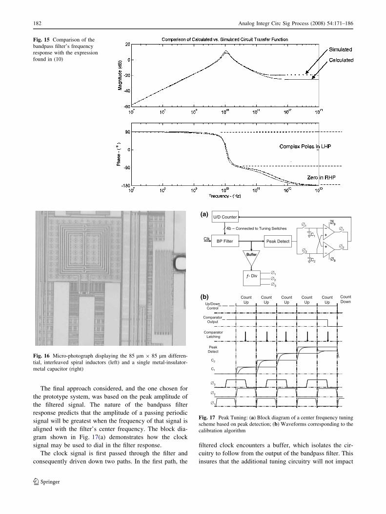
The final approach considered, and the one chosen for
the prototype system, was based on the peak amplitude of
the filtered signal. The nature of the bandpass filter
response predicts that the amplitude of a passing periodic
signal will be greatest when the frequency of that signal is
aligned with the filter’s center frequency. The block dia-
gram shown in Fig. 17(a) demonstrates how the clock
signal may be used to dial in the filter response.
The clock signal is first passed through the filter and
consequently driven down two paths. In the first path, the
filtered clock encounters a buffer, which isolates the cir-
cuitry to follow from the output of the bandpass filter. This
insures that the additional tuning circuitry will not impact
Fig. 15 Comparison of the
bandpass filter’s frequency
response with the expression
found in (10)
Fig. 16 Micro-photograph displaying the 85 lm 9 85 lm differen-
tial, interleaved spiral inductors (left) and a single metal-insulator-
metal capacitor (right)
U/D(a)
(b)
Counter
BP Filter
ƒ- Div
BufferBuffer
Peak Detect+_+_
+_+_
1
2
C2
C1
1
2
1
2
33
33
4b – Connected to Tuning Switches
Clk
3
Fig. 17 Peak Tuning: (a) Block diagram of a center frequency tuning
scheme based on peak detection; (b) Waveforms corresponding to the
calibration algorithm
182 Analog Integr Circ Sig Process (2008) 54:171–186
123

the quality of the final clock output negatively. Following
the buffer, the signal is fed into a frequency divider circuit
which outputs three lower frequency nonoverlapping clock
signals, /1, /2, and /3 with 90� of phase shift between
them, to be used for the sampling of the filtered clock
amplitude. These signals are also shown at the bottom of
the timing diagram found in Fig. 17(b).
The second path taken by the filtered clock signal passes
through a peak detection circuit which produces a DC
voltage whose DC level is relative to the peak voltage of
the alternating filtered clock signal. The signals /1 and /2
are then alternately used to sample the peak level of the
filtered clock. The timing diagram in Fig. 17(b) provides
an example of how the calibration should proceed.
1. First the peak detector output is sampled on the rising
edge of /1 and stored on capacitor C1.
2. The Up/Down counter, which is initially set to zero,
corresponding to the highest center frequency setting,
is increased by one and signal /2 samples the new
peak level and stores it on capacitor C2.
3. The two comparators shown in the schematic then
compare the two sampled levels on the falling edge of
signal /3 and the output of the upper comparator
passes its value to the counter which consequently
steps the tuning setting up or down accordingly. A
high comparator output signifies that the second
sampled value was greater and therefore the last
adjustment brought the filter response closer to the
desired response.
4. If the counter is incremented, the new peak level is
sampled by signal /1 and stored on C1.
5. The two samples are again compared and the output of
the lower comparator is passed to the counter on the
rising edge of /3.
6. The process continues until the most recently sampled
value is lower then the previous sample, indicating that
the filter is diverging from the optimal setting, at which
point the counter is decremented once to return to the
previous tuning setting and calibration is disabled.
From the circuit perspective, the tuning resolution is set
by the unit capacitance of the capacitor array. As a result, it
was decided that 4-bits of tuning control would provide
sufficient tuning range. Reducing the unit capacitance
further provided no benefit in simulation, as the parasitic
capacitance on the output node increases with each new
branch of the array and quickly becomes comparable in
size to the least significant tuning bit. Due to the relatively
low-Q value of the final filter (2.622), the required reso-
lution in the center frequency tuning resulting from a wider
passband at each tuning step was relaxed, providing a
second justification for the use of the 60 fF unit capaci-
tance in the array. In the final implementation, with the unit
load capacitance equal to 60 fF, the frequency step from
the ideal 5 GHz center frequency to the nearest settings
above and below were on the order of 200–400 MHz,
while the overall tuning range covered through the 16 steps
was 3.8–8.53 GHz (Fig. 18).
5 Performance of the clock filter
To verify the filter’s response to common noise events,
simulations were run in which power supply and common-
mode noise were superimposed onto the passing clock signal
and the peak-to-peak output jitter was noted.1 The worst case
common-mode noise sensitivity occured near 250 MHz, and
resulted in approximately 30 fs of jitter per millivolt of input
common-mode noise. Power supply noise sensitivity peaked
at the filter’s center frequency, and led to approximately 6fs
of jitter per millivolt of power supply noise. As an additional
experiment, an artificial input offset of 50 mV along with a
peak-to-peak power supply noise of 25 mV at the frequency
of maximum sensitivity was applied to the circuit. Simul-
taneously a 5 GHz clock exhibiting 25 mV of common-
mode noise at the frequency of maximum sensitivity was
passed through the filter and the simulated peak-to-peak
output jitter was observed to be 2.043 ps.
By integrating the simulated thermal noise at the output
to derive an equivalent rms noise level, and following the
discussed approach of scaling the rms noise level by the
inverse of the signal slewrate to approximate the rms jitter
level, the anticipated jitter generated by the circuit was
40.49 fs.
Fig. 18 4-bit tuning range of the proposed bandpass filter
1 All of the simulations reported correspond to the extracted
characteristics of the circuit, including an s-parameter representation
of the inductor layout.
Analog Integr Circ Sig Process (2008) 54:171–186 183
123

Jitter amplification was also considered. Figure 19 pre-
sents the jitter amplification of the circuit for several input
clock frequencies, with each curve corresponding to a
distinct 4-bit center frequency tuning setting. When the
filter center frequency is tuned to 5 GHz, the peak jitter
amplification around 3 GHz, as seen in the diagram, results
from an amplification of the clock’s second harmonic
through the filtering process. Conversely, when the clock
frequency equals the filter’s center frequency of 5 GHz, the
random jitter and DCD amplification are predicted to be
0.45–0.5 and 0.25, respectively.
Table 2 presents the final characteristics of the bandpass
filter, while Figs. 20–22 illustrate the impact of the
Fig. 19 Simulated jitter amplification versus filter center frequency
tuning
Table 2 Simulated filter characteristics and performance
Feature Value
Center frequency (fc) 5 GHz
Power dissipation 5.695 mW
Gain at fc 7.924 dB
Tuning range 3.8–8.53 GHz
On-chip spiral inductor value 1.92 nH
Inductor dimensions 85 lm 9 85 lm
Inductor quality factor 4.38
Total filter quality factor 2.622
Jitter amplification factor 0.4
Jitter generation 40.69 fs
Common-mode noise sensitivity 30 fs/mV
Power supply sensitivity 6 fs/mV
Fig. 20 Simulated impact of the proposed bandpass filter circuit on
random jitter
Fig. 21 Simulated impact of the proposed bandpass filter circuit on
DCD
Fig. 22 Simulated impact of the proposed bandpass filter circuit on a
sinusoidal jitter component
184 Analog Integr Circ Sig Process (2008) 54:171–186
123

bandpass filter on specific components of the overall clock
jitter. In Fig. 20 the bandpass filter is shown to reduce the
rms jitter level by a factor of 3.77. In a similar way,
Figs. 21 and 22 show the filter reducing peak-to-peak DCD
and sinusoidal jitter at a given frequency by factors of 3.57
and 4.29, respectively.
6 Conclusion
Past and present approaches to reducing clock jitter in
digital communication systems have typically counted on
the high frequency jitter attenuating nature of PLLs, while
the clock jitter is rarely addressed directly. Unfortunately,
the assumption that incorporating a PLL into the clock path
will eliminate clock signal integrity issues is often incor-
rect, as the jitter filtering characteristics of the PLL may
reduce the correlation between jitter events once common
to data signals and their associated forwarded sampling
clocks, and the PLL may actually contribute more jitter to
the passing clock than it removes.
In some cases, the use of a relatively low-Q bandpass
filter may serve to reduce clock jitter significantly without
the complexity of the PLL. One possible topology is the
fully differential, LC bandpass filter presented here. The
slow transient response of the circuit has an averaging
effect on the incoming edge timing, reducing both random
and high frequency periodic jitter components. At the same
time, the filter has proved effective in reducing the DC and
high frequency components of DCD. In fact, the very
nature of bandpass filters, being nearly ‘‘matched filters‘‘
for clock signals makes them somewhat ideal for these
types of signal conditioning. If the avoidance of such cir-
cuits in forwarded-clock systems of the past was due to the
anticipated noise and on-chip area required for imple-
mentation, the low power, relatively small and simple
design presented here makes bandpass filtering of high-
speed clocks in standard CMOS a viable solution to clock
timing uncertainty.
Acknowledgments This work was supported by the Intel Corpo-
ration with helpful suggestions from Bryan Casper of Intel’s Circuit
Research Lab, Hillsboro, Oregon, USA, and was originally developed
for incorporation into the system presented in [3] and a corresponding
patent application was filed under [9]. A small portion of this work
was also published previously in [5].
References
1. Proakis, J. G. (1995). Digital communications (3rd ed.). New
York: McGraw-Hill.
2. Sklar, B. (1988). Digital communications—fundamentals andapplications (1st ed.). New Jersey: Prentice Hall.
3. Casper, B., Jaussi, J., O’Mahony, F., Mansuri, M., Canagasaby, K.,
Kennedy, J., Yeung, E., & Mooney, R. (2006). A 20 Gb/s
forwarded clock transceiver in 90 nm CMOS. In Proceedings ofthe IEEE International Solid-State Circuits Conference.
4. Comer, D. T. (1995). VCO jitter reduction with bandpass filtering.
Electronic Letters, 31(1) IRE, 11–12.
5. Hollis, T. M., Comer, D. J., & Comer, D. T. (2005) Reduction of
duty cycle distortion through bandpass filtering. In Proceedings ofthe IEEE Conference on PhD Research in Microelectronics andElectronics (vol. 2, pp. 67–70).
6. Stojanovic, V., & Horowitz, M. (2003). Modeling and analysis of
high-speed links. In Proceedings of the IEEE Custom IntegratedCircuits Conference, September (pp. 589–594).
7. Ng, H., Farjad-Rad, R., Lee, M. J., Dally, W. J., Greer, T., Poulton,
J., Edmondson, J. H., Rathi, R., & Senthinathan, R. (2003). A
second-order semidigital clock recovery circuit based on injection
locking. IEEE Journal of Solid State Circuits, 38(12), 2101–2110.
8. Khoury, J. M. (1991). Design of a 15-MHz CMOS continuous-
time filter with on-chip tuning. IEEE Journal of Solid StateCircuits, 26(12), 1988–1997.
9. Casper, B. K., Hollis, T. M., Jaussi, J. E., Mooney, S. R.,
O’Mahony, F., & Mansuri, M. (2005). Forwarded clock filtering,
US Patent Applied For, December.
Timothy M. Hollis received
the B.S. degree in Electrical
Engineering from the University
of Utah, Salt Lake City, UT, in
2003 and the Ph.D. degree in
Electrical Engineering from
Brigham Young University,
Provo, UT, in April 2007. His
focus has been in the area of
channel equalization and jitter
attenuation circuits for high-
speed serial interconnects. As a
graduate student he interned
with both Micron Technology,
Inc., Boise, ID, and Intel Corporation’s Circuit Research Laboratory,
Hillsboro, OR. Following graduation, he joined Micron full-time,
researching signal integrity issues for future generations of high-
performance DRAM. Dr. Hollis received both the Micron Foundation
Undergraduate and Graduate Scholarships.
David J. Comer received the
B.S., M.S., and Ph.D. degrees
from San Jose State University,
the University of California
(Berkeley), and Washington
State University, respectively,
all in Electrical Engineering. He
has worked for IBM Corp.,
Pacific Electromagnetics, Law-
rence Livermore Laboratories,
and Intel Corporation. He began
his teaching career at the Uni-
versity of Idaho and has taught
at the University of Calgary and
California State University (CSU), Chico. He is presently a Professor
of Electrical and Computer Engineering at Brigham Young Univer-
sity (BYU), Provo, UT. He served as Chairman of the Division of
Analog Integr Circ Sig Process (2008) 54:171–186 185
123

Engineering at CSU, Chico and as Department Chair at BYU. While
at CSU, Chico, he served on the statewide Engineering Liaison
Committee and served as Chair of the Council of CSU Deans of
Engineering. He has published 12 textbooks and over 70 articles in
the field of circuit design. He has contributed sections to the Ency-
clopedia of Physical Science and Technology and holds eight patents.
Dr. Comer was given the Professional Achievement Award at CSU,
Chico, and was selected to receive the Karl G. Maeser Excellence in
Teaching Award at BYU. He has also held the College of Engineering
Research Chair at Brigham Young University.
186 Analog Integr Circ Sig Process (2008) 54:171–186
123


![a b c d k a e j a,m d a arXiv:1210.7877v1 [astro-ph.IM] 30 ... · microstrip waveguide, spectral bandpass filtering transmits only the desired frequency band, and superconduct-ing](https://img.pdfslide.us/doc/110x75/60626ab4d1c30c01523172f6/a-b-c-d-k-a-e-j-am-d-a-arxiv12107877v1-astro-phim-30-microstrip-waveguide.jpg)