Embed Size (px)
Citation preview

1
Band Tail Engineering in Kesterite Cu2ZnSn(S,Se)4
Thin-Film Solar Cells with 11.8% Efficiency
Myeng Gil Ganga,†, Seung Wook Shinb,†, Mahesh P. Suryawanshia, Uma V. Ghorpadea, Zhaoning
Songb, Jun Sung Janga, Jae Ho Yunc, Yanfa Yanb,*, Jin Hyeok Kima,*
aOptoelectronics Convergence Research Center and Department of Materials Science and
Engineering, Chonnam National University, 300, Yongbong-Dong, Buk-Gu, Gwangju 61186,
South Korea
bDepartment of Physics and Astronomy and Wright Center for photovoltaic Innovation and
Commercialization, University of Toledo, Toledo, Ohio, 43606, United States
cPhotovoltaic Laboratory, Korea Institute of Energy Research, 71-2, Jang-Dong, Yuesong-Gu,
Daejeon 34129, South Korea
AUTHOR INFORMATION
Corresponding Authors
*E-mail: [email protected] (Y. Yan)
*E-mail: [email protected] (J.H. Kim)
Author Contributions
†M. G. Gang and S. W. Shin contributed equally to this work

2
ABSTRACT
The efficiency of current kesterite Cu2ZnSn(Sx,Se1-x)4 (CZTSSe) thin-film solar cells is limited by
the large open-circuit voltage (Voc) deficit, which is associated with band tailing in CZTSSe.
Herein, we report a facile process, i.e., controlling the initial chamber pressure during the post-
deposition annealing, to effectively lower the band tail states in the synthesized CZTSSe thin films.
Through a detailed analysis of the external quantum efficiency derivative (dEQE/dλ) and low
temperature photoluminescence (LTPL) data, we find that the band tail states are significantly
influenced by the initial annealing pressure. After carefully optimizing the deposition processes
and device design, we are able to synthesize kesterite CZTSSe thin films with energy differences
between inflection of dEQE/dλ and LTPL as small as 10 meV. These kesterite CZTSSe thin films
enable the fabrication of solar cells with a champion efficiency of 11.8% with a low Voc deficit of
582 mV. The results suggest that controlling annealing process is an effective approach to reduce
the band tail in kesterite CZTSSe thin films.
Metal chalcogenide thin film solar cells (TFSCs) hold a great potential for producing clean
and affordable solar electricity because they offer exceptional opportunities for low cost
manufacturing of high performance photovoltaic (PV) modules.1-6 In particular, Cu(In,Ga)Se2
(CIGS) and CdTe TFSCs have already achieved high power conversion efficiencies (PCEs) over
22% and have shown steady growth in the renewable energy market.1-2, 7 In spite of the outstanding
performances, the widespread deployment of CIGS and CdTe TFSCs is hindered by the inclusion
of rare (e.g., In, Ga, and Te) and environmentally unfriendly (e.g., Cd) elements in the absorber
materials.8-9 The recently emerging kesterite-based absorber materials, such as Cu2ZnSnS4 (CZTS),

3
Cu2ZnSnSe4 (CZTSe), and Cu2ZnSn(Sx,Se1-x)4 (CZTSSe), have attracted significant attention due
to their low toxicity and earth-abundant elemental constitutions, direct and tunable bandgaps from
1.0 to 1.5 eV, high absorption coefficients of 104 cm-1, and high theoretical efficiencies of up to
30%.2, 10-13 The record PCE of CZTSSe-based TFSCs has been steadily increased to 12.6% in
20142, but the progress has stalled in recent years.
Despite their similarities, CZTSSe TFSCs significantly underperform their sister
technology CIGS TFSCs.7 One of the main reason limiting the performance of CZTSSe is the large
open-circuit voltage (Voc)-deficit, defined as Eg/q-Voc, where Eg is bandgap energy of the kesterite
absorber and q is the electron charge.14-16 The Voc deficit of the champion CZTSSe TFSCs (617
mV)2 is significantly larger than that of their CIGS counterparts (310 mV).7 Many studies attribute
this deficit to band tailing caused by the cationic disordering.14, 16-18 The natural complexity of the
quaternary compounds increases the likelihood of formation of various defects, especially the anti-
site defect complexes, which are believed to be the primary cause for the band tailing because of
their low defect formation energies.14, 19 These defects are likely formed during the high
temperature sulfurization (or selenization) process which promotes a random distribution of
cations in the crystal lattice, leading to the cationic disordering.20 To reduce the Voc-deficits of
CZTSSe based TFSCs, recent efforts have focused on identification and control of band tail states
in kesterite CZTSSe (see details in Table S1).5, 10, 12, 15, 17, 21-34 Among various approach, one
prospective pathway to mitigate band tailing is to develop a better control of the CZTSSe
synthesized process conditions, most importantly, the post-deposition annealing conditions to
suppress or remove cation site disorder and associated band tailing.
In this letter, we examine the interplay between the post-deposition annealing conditions
and the band tailing in the CZTSSe films by a systematic investigation of the dependence of
4
CZTSSe thin film properties on annealing pressures and a detailed comparison of the energy
difference between the inflection of external quantum efficiency derivative (dEQE)/dλ) and low
temperature photoluminescence (LTPL) for the corresponding CZTSSe TFSCs. We show that
band tail states in CZTSSe can be manipulated through a facile control of the initial chamber
pressure during the annealing process. With careful optimization of all component layers, we
achieve the champion CZTSSe TFSCs with a certificated PCE of 11.8%, a low Voc deficit of 582
mV, and the smallest value of energy difference between dEQE/dλ and LTPL (10 meV) measured
under an AM 1.5G illumination.
Our CZTSSe thin films are obtained by annealing sputtered and soft-annealed Zn/Sn/Cu metallic
precursors under a mixed S and Se vapor atmosphere as shown in Figure S1. Briefly, (i) a metallic precursor
with stacking order of Cu/Sn/Zn was deposited on Mo coated soda lime glass (SLG) substrates at 0 ºC by
sputtering; (ii) the metallic precursor was annealed at 300 ºC for 60 min under Ar atmosphere (i.e., `soft-
annealing process`) to obtain Cu-Zn and Cu-Sn alloys with smooth morphologies; (iii) the soft-annealed
precursor and chalcogen powders were placed in a graphite box (with a volume of ~ 406 cm3) in a rapid
thermal annealing (RTA) chamber; (iv) the chamber was evacuated to a base pressure of 1.0 x 10⁻³ Torr and
then the initial pressure was controlled at 400, 500, 600, and 700 Torr through controlling the amount of Ar
gas added to the chamber; (v) the chamber was heated up at a ramp rate of 10 ºC/s to 520 ºC and held
isothermal for 10 min; (vi) the annealed film was naturally cooled for 1 hour. The detailed pressure and
temperature profiles during the annealing process are shown in Figure S2 and S3. Experimental details are
provided in the Supporting Information.
We first investigate the impacts of initial chamber pressure on the formation of kesterite CZTSSe
by characterizing the structural, morphological, and compositional properties of CZTSSe films annealed
under differnet pressures. Figure 1a shows X-ray diffraction (XRD) patterns of CZTSSe thin films annealed
under different initial chamber pressures. All CZTSSe films show similar XRD patterns of three intense

5
diffraction peaks near 27.3˚, 45.2˚, and 53.7˚, corresponding to the (112), (220), and (312) planes, along
with three minor peaks (17.5 ˚, 36.4 ˚ and 66.0 ˚) of the CZTSe kesterite structure. The peaks belonging to
the CZTS kesterite phase also presents in the vicinity of the CZTSe peaks with higher diffraction angles
due to smaller ionic radius of S2− (0.184 nm) than Se2− (0.198 nm).3 However, it is known that distinguishing
the kesterite CZTS phase by analyzing XRD patterns from secondary phases, such as tetragonal or cubic
Cu2SnS3 (CTS) and cubic ZnS is difficult because their lattice constants are nearly identical. One promising
solution for phase classification in CZTSSe thin films is Raman spectroscopy measurements with different
excitation laser sources because Zn(S,Se) and Cu2Sn(S,Se)3 phases can be distinguished using 325 and 633
nm excitation laser sources, respectively (Figure S4).3 From three Raman spectra using different excitation
laser sources, no other phases are identified, indicating the formation of phase pure CZTSSe kesterite under
all annealing conditions.

6
Figure 1. (a) X-ray diffraction patterns and (b) Raman spectra using 514 nm exitation laser source
of CZTSSe thin films annealed under different initial chamber pressures. Red and blue dash lines in (a) and
(b) indicate peaks for Cu2ZnSnSe4 and Cu2ZnSnS4, respectively. Surface- and cross-sectional SEM images
of CZTSSe thin films annealed under the initial chamber pressure of (c, g) 400, (d, h) 500, (e, i) 600, and
(f, j) 700 Torr, respectively.
Figure 1c-f shows surface scanning electron microscopy (SEM) images of CZTSSe films annealed
under different pressures. All the films show smooth and dense morphology with grain size ranging from
0.5 to 1.5 μm. There is no significant difference regardless of initial chamber pressure. The cross-sectional
SEM images (Figure 1g-j) reveal simililar bi-layered microstructures in all the films, consisting of more
compact submicron sized grains on the top and smaller sized grains accompanied with voids at the bottom
region. In particular, the thickness of the top layer increases with increasing annealing pressure.
Additionally, the formation of interfacial Mo(S,Se)2 layer between CZTSSe and Mo back contact is not
observed, indicating a negligible thickness of less than 20 nm which is undetectable by SEM. Transmission
electron microscopy (TEM) image (Figure S5) confirms that the interface between CZTSSe and Mo back
contact layer is less than 20 nm. The Se/(S+Se) ratios for CZTSSe thin films as a function of initial chamber
pressure measured using X-ray fluorescence (XRF) and inductively coupled plasma mass spectrometry
(ICP-MS) characterizations as well as predicted from XRD and Raman spectra are shown in Table S2. The
results show that Se/(S+Se) ratio in the film is strongly dependent on the initial chamber pressure. The
measured and predicted Se/(S+Se) ratio slightly increases from 0.89 to 0.92~0.94 with increasing initial
chamber pressure, likely due to the different equilibrium partial pressures of S and Se gases during the
annealing process. The results suggest that S becomes more reactive with increasing initial chamber
pressure.

7
Figure 2. Device performance parameters of the CZTSSe TFSCs annealed under different initial chamber pressures,
including (a) Voc, (b) Jsc, (c) FF, and (d) η, measured under simulated AM 1.5G illumination. Each data set was
obtained from 6 solar cells. Blue symbols show average values.
To further investigate the influence of annealing pressure on solar cell performance, we fabricated
TFSCs using CZTSSe films annealed under different initial chamber pressures. Figure 2 shows the
distribution of PV performance parameters of these devices, and the representative current-voltage (J-V)
curves are shown in Figure S6a. The average and best performances of CZTSSe TFSCs increase when
initial chamber pressure is increased from 400 to 500 Torr and then decrease when the pressure is further
increased. Interestingly, the initial chamber pressure has larger impacts on Voc and FF than on Jsc (See Table
S3 for details). The smallest Voc-deficit of 609 mV is achieved in CZTSSe TFSCs annealed under an initial
chamber pressure of 500 Torr, while other devices show the Voc-deficit values of over 670 mV.

8
To understand the relationship between Voc-deficit caused by band tail states and performance of
CZTSSe TFSCs as a function of initial chamber pressure, we compare the energy differences between the
effective bandgap measured from the inflection of EQE, i.e., the peak in dEQE/dλ, and the bandgap
measured from LTPL spectra (Figure 3). For all the CZTSSe samples, LTPL peaks are shifted to lower
energies relative to the bandgaps determined by the EQE spectra. The energy differences determined from
the dEQE/dλ and LTPL data are 110, 27, 38, and 42 meV for the device with CZTSSe films annealed under
the initial pressure of 400, 500, 600, and 700 Torr, respectively, showing the trend consistent with the
variation of PV performance, especially the VOC in CZTSSe TFSCs (Figure 2a). The large energy difference
between bandgaps measured from dEQE/dλ and LTPL is mainly attributed to antisite defect complexes in
the CZTSSe layers, such as Vcu+ SnZn and CuZn+SnZn, which introduce nonradiative recombination centers
or band tailing.2, 16, 26, 32 Additionally, notable differences are observed in the subbandgap absorption of
these CZTSSe films, determined by the EQE data followed a reported method (Figure S7).14 The 500 Torr
sample exhibits the lowest subbandgap absorption coefficient, indicating the lowest band tail state density
among the samples. The combined results suggest that precise control of the initial chamber pressure can
effectively reduce the band tailing in the CZTSSe films and enhance device performance of CZTSSe TFSCs.
The underlying mechanisms for lower band tail states at higher initial chamber pressures are yet to be
determined. Some possible hypotheses include (i) the high external pressure may reduce Sn loss and,
consequently, reduce Sn-related antisite defects such as VSn and ZnSn; (ii) the high initial chamber pressure
may enhance the Se contents near surface region, leading to less anitsite defect density than that with a
lower Se content. We are undergoing investigations on different experimental conditions, such as
substitution of Ag at Cu site, metal stacking order of the precursor, soft-annealing process (i.e., holding
time, temperature, and atmosphere), and sulfo-selenization process (i.e., hold time, step annealing process,
temperature, and etc.) for CZTSSe thin films, by using various characterization techniques to clearly explain
the relationship between the initial chamber pressure and the reduced band tails.

9
Figure 3. EQE (black), LTPL (blue), and dEQE/dλ (red circles) spectra of CZTSSe TFSCs
annealed under the initial chamber pressure of (a) 400, (b) 500, (c) 600, and (d) 700 Torr.
The aforementioned results motivate us to further optimize the fabrication processes of TFSCs based
on CZTSSe films annealed under the initial pressure of 500 Torr. The optimization processes include (i)
reducing CdS layer thickness, (ii) introducing a MgF2 anti-reflection layer, and (iii) fine tuning
compositional ratio of CZTSSe, as shown in Figure S8. Figure 4 shows (a) J-V and (b) EQE curves of the
champion CZTSSe device with a PCE of 11.8%, a Voc of 485 mV, a Jsc of 37.50 mA/cm2, and a FF of
64.91%, measured under an AM 1.5G illumination. The result was certified by Korea Institute of Energy
Research (KIER), as shown in Figure S9. The EQE spectrum of this device shows nearly 95% in the visible
region and then decreases in the longer wavelength region, as shown in Figure 4b. Importantly, the Voc-
deficit of this champion device (~582 mV), with a 10 meV energy difference between the bandgaps
measured from dEQE/dλ and LTPL, is among the smallest values for kesterite TFSCs reported in literature.
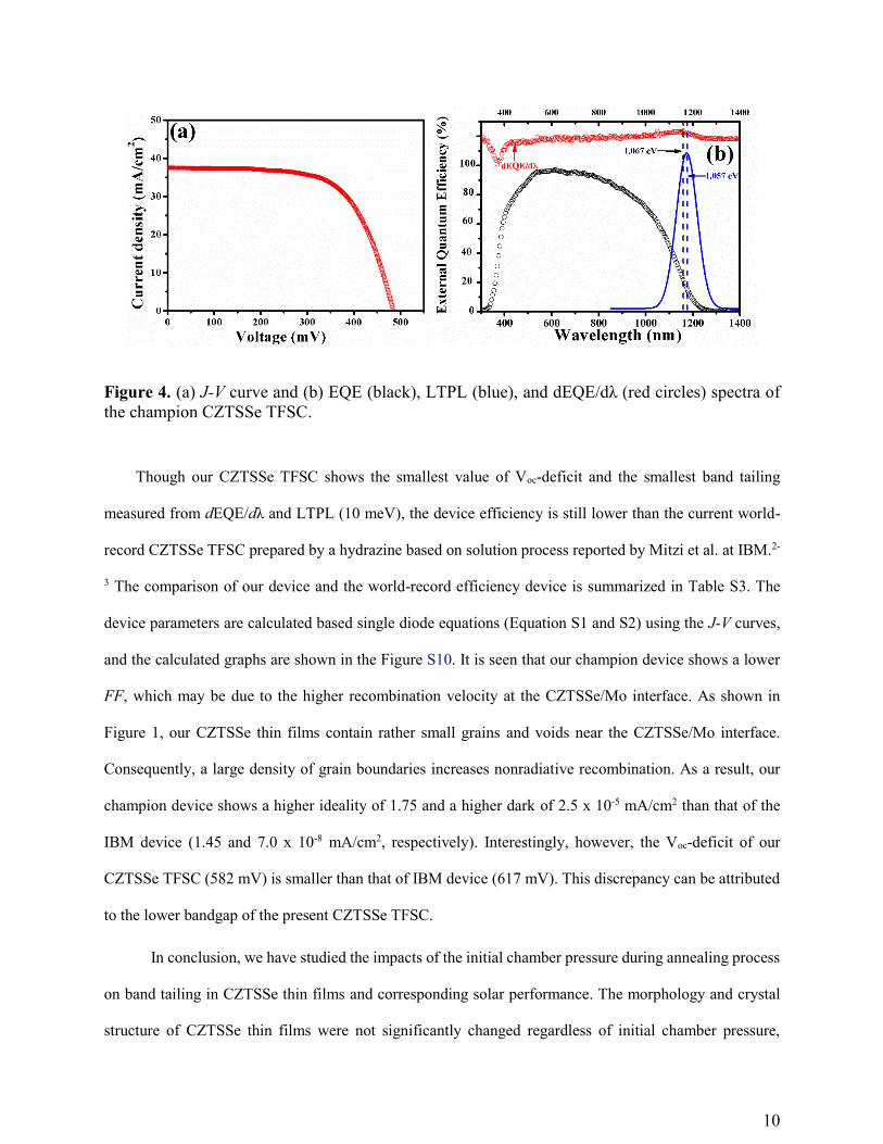
10
Figure 4. (a) J-V curve and (b) EQE (black), LTPL (blue), and dEQE/dλ (red circles) spectra of
the champion CZTSSe TFSC.
Though our CZTSSe TFSC shows the smallest value of Voc-deficit and the smallest band tailing
measured from dEQE/dλ and LTPL (10 meV), the device efficiency is still lower than the current world-
record CZTSSe TFSC prepared by a hydrazine based on solution process reported by Mitzi et al. at IBM.2-
3 The comparison of our device and the world-record efficiency device is summarized in Table S3. The
device parameters are calculated based single diode equations (Equation S1 and S2) using the J-V curves,
and the calculated graphs are shown in the Figure S10. It is seen that our champion device shows a lower
FF, which may be due to the higher recombination velocity at the CZTSSe/Mo interface. As shown in
Figure 1, our CZTSSe thin films contain rather small grains and voids near the CZTSSe/Mo interface.
Consequently, a large density of grain boundaries increases nonradiative recombination. As a result, our
champion device shows a higher ideality of 1.75 and a higher dark of 2.5 x 10⁻⁵ mA/cm2 than that of the
IBM device (1.45 and 7.0 x 10⁻⁸ mA/cm2, respectively). Interestingly, however, the Voc-deficit of our
CZTSSe TFSC (582 mV) is smaller than that of IBM device (617 mV). This discrepancy can be attributed
to the lower bandgap of the present CZTSSe TFSC.
In conclusion, we have studied the impacts of the initial chamber pressure during annealing process
on band tailing in CZTSSe thin films and corresponding solar performance. The morphology and crystal
structure of CZTSSe thin films were not significantly changed regardless of initial chamber pressure,

11
however, the device performance of CZTSSe TFSCs was strongly dependent on initial chamber pressure.
In particular, the analysis on the dEQE/dλ and LTPL data revealed that band tail defect densities in CZTSSe
films can be controlled by the initial annealing pressure. Using this strategy, we demonstrated the best
CZTSSe TFSC with a PCE of 11.8% with a record low Voc-deficit of 582 mV, and a small energy difference
of 10 meV between bandgaps measured from dEQE/dλ and LTPL. This facile process could provide an
effective approach for large scale manufacturing of CZTSSe TFSCs.
EXPERIMENTAL METHODS
The Cu-Sn-Zn stacked metallic precursor thin films were deposited on Mo coated soda lime glass
substrates using DC sputtering technique at 0 ºC. The precursor thin films were annealed under Ar
atmosphere to form the Cu-Zn and Cu-Sn alloys at 300 ºC for 60 min. To synthesize the CZTSSe
thin films, the chalcogenide powders such as S and Se and precursor thin films were placed in a
graphite box in a closed isothermal chamber system and heated to 520 ºC for 10 min. The annealing
chamber including precursor thin film, chalcogenide powder in the graphite box was evacuated to
a base pressure of 5.0 x 10⁻³ Torr, and then the initial pressures were controlled as 400, 500, 600,
and 700 Torr through adjusting Ar gas flow to the chamber. The TFSCs were fabricated with a
multi-layered structure of MgF2/Al/Al-Ni/AZO/i-ZnO/CdS/CZTSSe/Mo/Glass. The detailed
experimental conditions and characterizations are given in the Supporting Information.
ASSOCIATED CONTENT
Temperature and pressure profiles during whole annealing process, preparation of CZTSSe films
and fabrication processes of Al/Al-Ni/AZO/i-ZnO/CdS/CZTSSe/Mo/Glass structured solar cells,
Raman spectra using different exitation laser sources, TEM image at interface between CZTSSe

12
and Mo back layer, measured J-V curves, –ln(1-EQE) vs. photo energy plots, and certificated
champon efficiency, efficieny evolution map through optimizing process, dJ/dV vs. voltage, dV/dJ
vs. (J + Jsc)-1, (J + Jsc –GV) vs. (V-RJ) plots, summarized device parameters.
AUTHOR INFORMATION
ORCID
Seung Wook Shin: 0000-0002-3396-2535
Mahesh P. Suryawanshi: 0000-0003-4711-7655
Uma V. Ghorpade: 0000-0001-8631-7030
Zhaoning Song: 0000-0002-6677-0994
Yanfa Yan: 0000-0003-3977-5789
Jin Hyeok Kim : 0000-0003-4711-7655
E-mail:[email protected] (M.G. Gang), [email protected] (S.W. Shin),
[email protected] (M.P. Suryawanshi), [email protected] (U.V.
Ghorpade), Jun Sung Jang ([email protected]), [email protected] (Z. Song),
[email protected] (J.H. Yun)
Notes
The authors declare no competing financial interest.
ACKNOWLEDGMENT
This work was supported by the Human Resources Development program (No. 20164030201310)
of the Korea Institute of Energy Technology Evaluation and Planning (KETEP) grant funded by
the Korea government Ministry of Trade, Industry and Energy and was partially supported by the
Technology Development Program to Solve Climate Changes of the National Research
Foundation (NRF) funded by the Ministry of Science, ICT & Future Planning (2016936784). Work

13
at University of Toledo was supported by NSF under contract no ECCS-1665028 and DMR-
1534686
TOC GRAPHICS
REFERENCES
(1) Hong, C. W.; Shin, S. W.; Suryawanshi, M. P.; Gang, M. G.; Heo, J.; Kim, J. H., Chemically
Deposited CdS Buffer/Kesterite Cu2znsns4 Solar Cells: Relationship between CdS Thickness and Device
Performance. ACS Appl. Mater. Interfaces 2017, 9, 36733-36744.
(2) Wang, W.; Winkler, M. T.; Gunawan, O.; Gokmen, T.; Todorov, T. K.; Zhu, Y.; Mitzi, D. B.,
Device Characteristics of CZTSSe Thin‐Film Solar Cells with 12.6% Efficiency. Adv. Energy Mater.2014,
4, 1301465.
(3) Gang, M. G.; Shin, S. W.; Hong, C. W.; Gurav, K. V.; Gwak, J.; Yun, J. H.; Lee, J. Y.; Kim, J. H.,
Sputtering Processed Highly Efficient Cu2ZnSn(S,Se)4 Solar Cells by a Low-Cost, Simple,
Environmentally Friendly, and up-Scalable Strategy. Green Chem. 2016, 18, 700-711.
(4) Pinto, A. H.; Shin, S. W.; Aydil, E. S.; Penn, R. L., Selective Removal of Cu2-X(S,Se) Phases from
Cu2ZnSn(S,Se)4 Thin Films. Green Chem. 2016, 18, 5814-5821.
(5) Pinto, A. H.; Shin, S. W.; Sharma, A.; Penn, R. L.; Aydil, E. S., Synthesis of Cu2(Zn1-XCox)SnS4
Nanocrystals and Formation of Polycrystalline Thin Films from Their Aqueous Dispersions. J. Mater.
Chem. A 2018, 6, 999-1008.
(6) Suryawanshi, M.; Shin, S. W.; Ghorpade, U.; Song, D.; Hong, C. W.; Han, S.-S.; Heo, J.; Kang, S.
H.; Kim, J. H., A Facile and Green Synthesis of Colloidal Cu2ZnSnS4 Nanocrystals and Their Application
in Highly Efficient Solar Water Splitting. J. Mater. Chem. A 2017, 5, 4695-4709.
(7) Jackson, P.; Wuerz, R.; Hariskos, D.; Lotter, E.; Witte, W.; Powalla, M., Effects of Heavy Alkali
Elements in Cu(in,Ga)Se2 Solar Cells with Efficiencies up to 22.6%. Phys. Status Sol. (RRL) – Rap. Res.
Lett. 2016, 10, 583-586.

14
(8) Ford, G. M.; Guo, Q.; Agrawal, R.; Hillhouse, H. W., Earth Abundant Element Cu2Zn(Sn1−XGex)S4
Nanocrystals for Tunable Band Gap Solar Cells: 6.8% Efficient Device Fabrication. Chem.Mater. 2011,
23, 2626-2629.
(9) Son, D.-H.; Kim, D.-H.; Park, S.-N.; Yang, K.-J.; Nam, D.; Cheong, H.; Kang, J.-K., Growth and
Device Characteristics of CZTSSe Thin-Film Solar Cells with 8.03% Efficiency. Chem. Mater. 2015, 27,
5180-5188.
(10) Haass, S. G.; Andres, C.; Figi, R.; Schreiner, C.; Bürki, M.; Romanyuk, Y. E.; Tiwari, A. N.,
Complex Interplay between Absorber Composition and Alkali Doping in High‐Efficiency Kesterite Solar
Cells. Adv. Energy Mater. 2018, 8, 1701760.
(11) Pundsack, T. J.; Chernomordik, B. D.; Béland, A. E.; Aydil, E. S.; Blank, D. A., Excited-State
Dynamics in CZTS Nanocrystals. J. Phys. Chem. Lett. 2013, 4, 2711-2714.
(12) Shin, D.; Ngaboyamahina, E.; Zhou, Y.; Glass, J. T.; Mitzi, D. B., Synthesis and Characterization
of an Earth-Abundant Cu2BaSn(S,Se)4 Chalcogenide for Photoelectrochemical Cell Application. J. Phys.
Chem. Lett. 2016, 7, 4554-4561.
(13) Thompson, M. J.; Ruberu, T. P. A.; Blakeney, K. J.; Torres, K. V.; Dilsaver, P. S.; Vela, J., Axial
Composition Gradients and Phase Segregation Regulate the Aspect Ratio of Cu2ZnSnS4 Nanorods. J. Phys.
Chem. Lett. 2013, 4, 3918-3923.
(14) Gokmen, T.; Gunawan, O.; Todorov, T. K.; Mitzi, D. B., Band Tailing and Efficiency Limitation
in Kesterite Solar Cells. Appl. Phys. Lett. 2013, 103, 103506.
(15) Neuschitzer, M.; Marquez, J.; Giraldo, S.; Dimitrievska, M.; Placidi, M.; Forbes, I.; Izquierdo-
Roca, V.; Pérez-Rodriguez, A.; Saucedo, E., Voc Boosting and Grain Growth Enhancing Ge-Doping
Strategy for Cu2ZnSnSe4 Photovoltaic Absorbers. J. Phys. Chem. C 2016, 120, 9661-9670.
(16) Rey, G.; Larramona, G.; Bourdais, S.; Choné, C.; Delatouche, B.; Jacob, A.; Dennler, G.;
Siebentritt, S., On the Origin of Band-Tails in Kesterite. Sol. Energy Mater. Sol. Cells 2018, 179, 142-151.
(17) Xie, H.; López-Marino, S; Olar, T.; Sánchez, Y.; Neuschitzer, M.; Oliva, F.; Giraldo, S.; Izquierdo-
Roca, V.; Lauermann. I.; Pérez-Rodríguez, A.; Saucedo. E., Impact of Na Dynamics at the
Cu2ZnSn(S,Se)4/CdS Interface During Post Low Temperature Treatment of Absorbers. ACS Appl. Materi.
Interfaces 2016, 8, 5017-5024.
(18) Rey, G.; Larramona, G.; Bourdais, S.; Choné, C.; Delatouche, B.; Jacob, A.; Dennler, G.;
Siebentritt, S., On the Origin of Band-Tails in Kesterite. Sol. Energy Mater. Sol. Cells 2018, 179, 142-151.
(19) Chen, S.; Yang, J.-H.; Gong, X. G.; Walsh, A.; Wei, S.-H., Intrinsic Point Defects and Complexes
in the Quaternary Kesterite Semiconductor Cu2ZnSnS4. Phys. Rev. B 2010, 81, 245204.
(20) Shin, D.; Saparov, B.; Mitzi, D. B., Photovoltaic Materials: Defect Engineering in Multinary Earth‐
Abundant Chalcogenide Photovoltaic Materials Adv. Energy Mater. 2017, 7, 1602366
(21) Lopez-Marino, S.; Sánchez, Y.; Espíndola-Rodríguez, M.; Alcobé, X.; Xie, H.; Neuschitzer, M.;
Becerril, I.; Giraldo, S.; Dimitrievska, M.; Placidi, M.; Fourdrinier, L. Izquierdo-Roca, V.; Pérez-
Rodríguezad, A.; Saucedo, E. Alkali Doping Strategies for Flexible and Light-Weight Cu2ZnSnSe4 Solar
Cells. J. Mater. Chem. A 2016, 4, 1895-1907.
(22) Tai, K. F.; Fu, D.; Chiam, S. Y.; Huan, C. H. A.; Batabyal, S. K.; Wong, L. H., Antimony Doping
in Solution‐Processed Cu2ZnSn(S,Se)4 Solar Cells. ChemSusChem 2015, 8, 3504-3511.
(23) Kim, I.; Kim, K.; Oh, Y.; Woo, K.; Cao, G.; Jeong, S.; Moon, J., Bandgap-Graded Cu2Zn(Sn1–
XGex)S4 Thin-Film Solar Cells Derived from Metal Chalcogenide Complex Ligand Capped Nanocrystals.
Chem. Mater. 2014, 26, 3957-3965.
(24) Sun, R.; Zhuang, D.; Zhao, M.; Gong, Q.; Scarpulla, M.; Wei, Y.; Ren, G.; Wu, Y., Beyond 11%
Efficient Cu2ZnSn(Se,S)4 Thin Film Solar Cells by Cadmium Alloying. Sol. Energy Mater. Sol. Cells 2018,
174, 494-498.

15
(25) Yan, C.; Sun, K.; Huang, J.; Johnston, S.; Liu, F.; Puthen Veettil, B.; Sun, K.; Pu, A.; Zhou, F.; A.
Stride, J.; A. Green, M.; Hao, X., Beyond 11% Efficient Sulfide Kesterite Cu2(Zn1-xCdx)SnS4 Solar Cell:
Effects of Cadmium Alloying. ACS Energy Lett. 2017, 2, 930-936.
(26) Li, J.; Wang, D.; Li, X.; Zeng, Y.; Zhang, Y., Cation Substitution in Earth‐Abundant Kesterite
Photovoltaic Materials. Adv. Sci. 2018, 5, 1700744.
(27) Tiwari, D.; Koehler, T.; Lin, X.; Harniman, R.; Griffiths, I.; Wang, L.; Cherns, D.; Klenk, R.;
Fermin, D. J., Cu2ZnSnS4 Thin Films Generated from a Single Solution Based Precursor: The Effect of Na
and Sb Doping. Chem. Mater. 2016, 28, 4991-4997.
(28) Giraldo, S.; Thersleff, T.; Larramona, G.; Neuschitzer, M.; Pistor, P.; Leifer, K.; Pérez‐Rodríguez,
A.; Moisan, C.; Dennler, G.; Saucedo, E., Cu2ZnSnSe4 Solar Cells with 10.6% Efficiency through
Innovative Absorber Engineering with Ge Superficial Nanolayer. Prog. Photovolt. Res. Appl. 2016, 24,
1359-1367.
(29) Khadka, D. B.; Kim, S.; Kim, J., Effects of Ge Alloying on Device Characteristics of Kesterite-
Based CZTSSe Thin Film Solar Cells. J. Phys. Chem. C 2016, 120, 4251-4258.
(30) Bag, S.; Gunawan, O.; Gokmen, T.; Zhu, Y.; Mitzi, D. B., Hydrazine-Processed Ge-Substituted
Cztse Solar Cells. Chem. Mater. 2012, 24, 4588-4593.
(31) Fu, J.; Tian, Q.; Zhou, Z.; Kou, D.; Meng, Y.; Zhou, W.; Wu, S., Improving the Performance of
Solution-Processed Cu2ZnSn(S,Se)4 Photovoltaic Materials by Cd2+ Substitution. Chem. Mater. 2016, 28,
5821-5828.
(32) Salomé, P. M. P.; Rodriguez-Alvarez, H.; Sadewasser, S., Incorporation of Alkali Metals in
Chalcogenide Solar Cells. Sol. Energy Mater. Sol. Cells 2015, 143, 9-20.
(33) Yang, Y.; Huang, L.; Pan, D., New Insight of Li-Doped Cu2ZnSn(S,Se)4 Thin Films: Li-Induced
Na Diffusion from Soda Lime Glass by a Cation-Exchange Reaction. ACS Appl. Mater. Interfaces 2017, 9,
23878-23883.
(34) Nguyen, T. H.; Kawaguchi, T.; Chantana, J.; Minemoto, T.; Harada, T.; Nakanishi, S.; Ikeda, S.,
Structural and Solar Cell Properties of a Ag-Containing Cu2ZnSnS4 Thin Film Derived from Spray
Pyrolysis. ACS Appl. Mater. Interfaces 2018, 10, 5455-5463


![Long Tail Vs Short Tail Keywords in ROI Perspective [Infographic]](https://img.pdfslide.us/doc/110x75/55cdf90fbb61ebf25b8b4663/long-tail-vs-short-tail-keywords-in-roi-perspective-infographic.jpg)