Embed Size (px)
Citation preview

© 2011 ANSYS, Inc. September 26, 2011
1
Balanced Amplifier in
Package on Board
Tony Donisi
Eldon Staggs

© 2011 ANSYS, Inc. September 26, 2011
2
Introduction
Demonstrate MMIC Balanced Amplifier design flow
• Linear and Non-Linear Design
• Amplifier incorporated into package
• System in packages and board
Evaluate System performance
• Non-linear circuit evaluation of Amplifiers
• Linear evaluation of Hybrid combiners
• Electromagnetic evaluation of packages on board
• Co-simulation of entire system

© 2011 ANSYS, Inc. September 26, 2011
3
Agenda
Design Environment
• Design Technology and Management
• Designer Links
• HFSS – Solver on Demand
System details
• Balanced Amplifier overview
• MMIC Amplifier design
• Hybrid design
System on board design
• Amplifier in Package
• Entire design on board

© 2011 ANSYS, Inc. September 26, 2011
4
Overview: Chip in Package

© 2011 ANSYS, Inc. September 26, 2011
5
Overview: Package to Board

© 2011 ANSYS, Inc. September 26, 2011
6
Design Environment

© 2011 ANSYS, Inc. September 26, 2011
7
Ansoft Designer Overview
Design Technology
• Circuit & System Analysis
– Time and Frequency Domain
• Electromagnetic Analysis
• Solver on Demand
– HFSS, PlanarEM, Nexxim and HSPICE
Design Management
• Hierarchical Schematic and Layout (2D/3D)
• Design Exploration
– Parameterization, Optimization, Sensitivity & Statistical
• Bi-directional Links to Field Solvers
– HFSS, PlanarEM, SIwave, Q3D, 2D Extractor
• 3rd Party Links for Models and Geometry
High Performance Computing (Multi-core/GPU)

© 2011 ANSYS, Inc. September 26, 2011
8
Design
Management
Property
Management
Design
Entry
Simulation
Management
Ansoft Designer User Interface
Post-Processing
Layout
© 2011 ANSYS, Inc. September 26, 2011
9
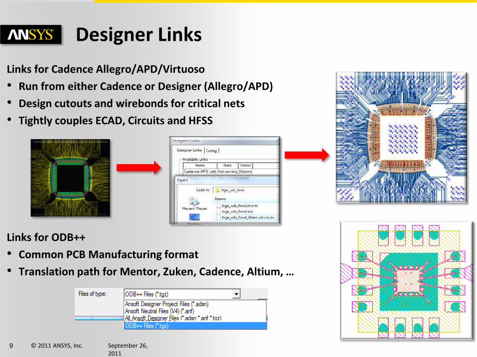
Designer Links
Links for Cadence Allegro/APD/Virtuoso
• Run from either Cadence or Designer (Allegro/APD)
• Design cutouts and wirebonds for critical nets
• Tightly couples ECAD, Circuits and HFSS
Links for ODB++
• Common PCB Manufacturing format
• Translation path for Mentor, Zuken, Cadence, Altium, …

© 2011 ANSYS, Inc. September 26, 2011
10
Ansoft Designer HFSS - Solver on Demand
HFSS - Solver on Demand • Intuitive PCB design entry alternative for HFSS • Chips, packages, channels, modules, … • HFSS / PlanarEM engine selection at runtime
3D Full-wave FEM Technology
• Designer layouts simulated with HFSS – Boundaries handled automatically – Excitations with a mouse click – Finite dielectrics and ground supported
• Terminal Excitations (Wave and Lumped Gap Port) – Single ended and Differential – Vertical and Horizontal – Coaxial, CPW and Grounded CPW
© 2011 ANSYS, Inc. September 26, 2011
11
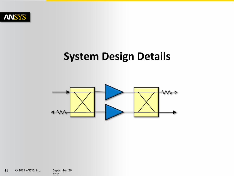
System Design Details

© 2011 ANSYS, Inc. September 26, 2011
12
Balanced Amplifier
What is a Balanced Amplifier?
• Two nearly identical amplifiers in parallel
• Amplifiers between two 90° hybrids
– Reflections cancel at I/O ports through hybrid
G
G 02VG
902VG
90VG
0V
01802
02
G
G VV

© 2011 ANSYS, Inc. September 26, 2011
13
Balanced Amplifier
Why used a Balanced Amplifier?
• Amplifiers optimized without concern of loading
– Noise Figure, Flatness, etc.
• Linear range and Max power increase by 3dB
• Reflections absorbed by loads at isolation ports
G
G 02VG
902VG
90VG
0V
01802
02
G
G VV

© 2011 ANSYS, Inc. September 26, 2011
14
Balanced Configuration Operation
.5A - f- 90º- 90º
A 0º .707A
.707A - 90º
.5A - f
.5A - f- 90º- 90º
- 90º
.5A - f- 90º- 90º
0
A - f2
A
2
A
45º
90°
.5A - f- 180º
.5A - f- 180º
.5A - f- 180º
f- 90º
f
90°

© 2011 ANSYS, Inc. September 26, 2011
15
Design Description
• Balanced Amplifier
• Combine two MMIC Amplifiers in parallel
• Incorporate amplifiers in separate packages
• Combine Amplifiers and 90° Hybrids on board
• Include on-board biasing for amplifiers

© 2011 ANSYS, Inc. September 26, 2011
16
MMIC Amplifier Design

© 2011 ANSYS, Inc. September 26, 2011
17
MMIC Amplifier Details
Power Amplifier
• Modeled in Designer with UMS design kit
• UMS pHEMT Process
• 10GHz center frequency
• Multiple Gain stages for increased output
• Wilkinson dividers to distribute power
• Compression determined by final stage
• Linear region and compression level increased
• Reactive matching
• Transmission line sections designed for 10GHz
© 2011 ANSYS, Inc. September 26, 2011
18
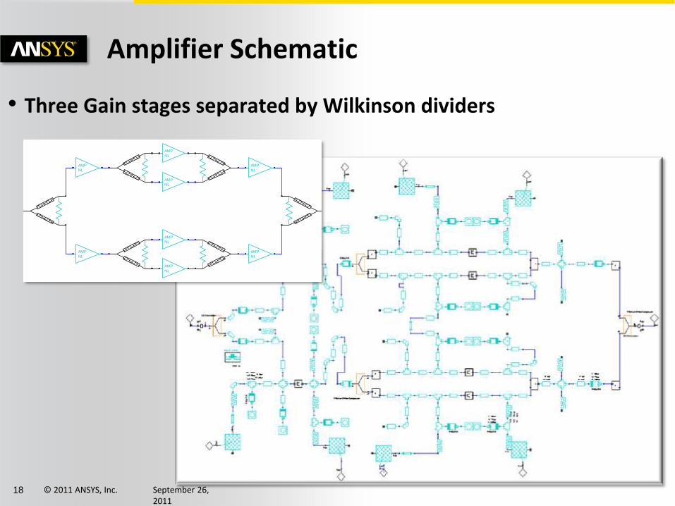
Amplifier Schematic
• Three Gain stages separated by Wilkinson dividers
AMP
NL
AMP
NL
AMP
NL
AMP
NL
AMP
NL
AMP
NL
AMP
NL
AMP
NL
Port1 Port2

© 2011 ANSYS, Inc. September 26, 2011
19
Amplifier Response
• Three amplification stages produce 22dB of gain
• Input compression point around 11dBm
Power = 30dBm
P1dB = 11dBm
F=10GHz
Gain = 22dB

© 2011 ANSYS, Inc. September 26, 2011
20
Amplifier Layout
• 1

© 2011 ANSYS, Inc. September 26, 2011
21
Branchline Hybrid Design

© 2011 ANSYS, Inc. September 26, 2011
22
90º Hybrid Design Overview
• Hybrid Applications
• Power Splitter / Combiner • Load on one of the input / output ports, respectively
• Sum and Difference outputs • Two inputs to hybrid
• 90º Hybrid Features
• Power Splitter • Second input port is terminated
• Quarter wavelength lines
• Series lines have lower imedance
• Output ports are 90º out of phase with each other
4L
2ZZ 0
/
4L
ZZ 0

© 2011 ANSYS, Inc. September 26, 2011
23
90º Hybrid Design Overview
• Physical Modeling
• Implement with transmission lines
• Conserve space by bending series lines
• Parameterize lengths and widths
• Analyze electromagnetically to account for all effects
• Optimize and Tune to 10GHz
5.00 7.50 10.00 12.50 15.00F [GHz]
-30.00
-25.00
-20.00
-15.00
-10.00
-5.00
0.00
Y1
BranchlineIdeal Linear Response ANSOFT
Curve Info
dB(S(Port1,Port1))
dB(S(Port1,Port2))
dB(S(Port1,Port3))
dB(S(Port1,Port4))

© 2011 ANSYS, Inc. September 26, 2011
24
90º Hybrid Design Overview
• Physical Modeling
• Implement with transmission lines
• Conserve space by bending series lines
• Parameterize lengths and widths
• Analyze electromagnetically to account for all effects
• Optimize and Tune to 10GHz
5.00 7.50 10.00 12.50 15.00F [GHz]
-30.00
-25.00
-20.00
-15.00
-10.00
-5.00
0.00
Y1
BranchlineIdeal Linear Response ANSOFT
Curve Info
dB(S(Port1,Port1))
dB(S(Port1,Port2))
dB(S(Port1,Port3))
dB(S(Port1,Port4))

© 2011 ANSYS, Inc. September 26, 2011
25
90º Hybrid Design Setup
• Hybrid Parameterization
• Wavelength, width and feed length
• HFSS – Solver on Demand
• HFSS analysis directly in Designer
• View mesh, airbox and parameterization
Final HFSS Mesh
Port1
Port4
Port2
Port3

© 2011 ANSYS, Inc. September 26, 2011
26
Hybrid Parameterized Analysis
• Build Model from parametric solutions • Coarse sweep over each parameter
• Distributed solve for speed up
• Circuit Model of HFSS solution • Circuit simulation interpolates solution space
• EM accuracy at circuit speeds

© 2011 ANSYS, Inc. September 26, 2011
27
Hybrid Real Time EM Tuning
• Solved Parametrically
• Tuned in real time
5.00 7.50 10.00 12.50 15.00F [GHz]
-35.00
-30.00
-25.00
-20.00
-15.00
-10.00
-5.00
0.00
Y1
Test HybridTuned Response ANSOFT
Curve Info
dB(S(Port1,Port1))Lambda4='144mil' Larm='125mil' W35='6.7mil'
dB(S(Port1,Port2))Lambda4='144mil' Larm='125mil' W35='6.7mil'
dB(S(Port1,Port3))Lambda4='144mil' Larm='125mil' W35='6.7mil'
dB(S(Port1,Port4))Lambda4='144mil' Larm='125mil' W35='6.7mil'
Lambda/4 = 144mil
W35 = 6.7mil
Larm = 125mil

© 2011 ANSYS, Inc. September 26, 2011
28
Include Package Transition Effects
• Additional effects • Wirebonds
• Vias
• Transitions
• Package
• Include "partial package" in hybrid analysis • Vary arm lengths to tune hybrids
© 2011 ANSYS, Inc. September 26, 2011
29
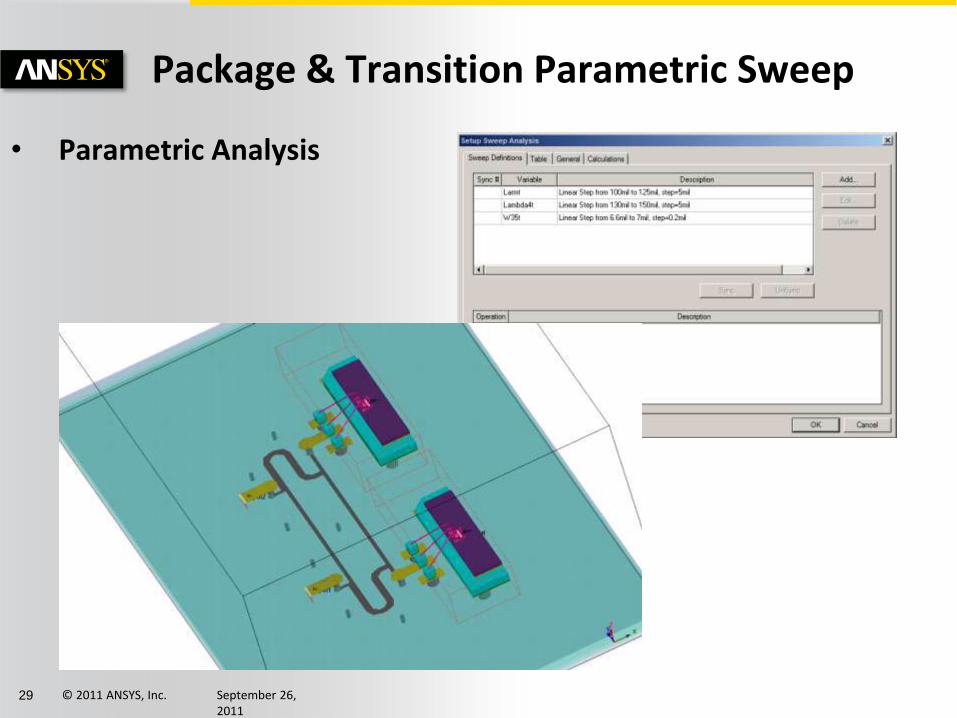
Package & Transition Parametric Sweep
• Parametric Analysis

© 2011 ANSYS, Inc. September 26, 2011
30
Dual Hybrid Testing
• Check parallel operation • Validate balanced amp configuration
• Amplifiers added in at final testing
• Tune parametric model
• Demonstrates • Insertion and Return Loss
• Isolation functionality
• Design Integrity
Port1 Port2
Port3
Port4
Test HybridTest Hybrid
P=40mil
W=3.7mil
P=40mil
W=3.7mil

© 2011 ANSYS, Inc. September 26, 2011
31 Port1Port2
Port3 Port4
Port1
Port4
Port2
Port3
U2Test Hybrid
Pin1
Pin2
Pin3
Pin4Port1
Port4
Port2
Port3
Pin1
Pin2
Pin3
Pin4
U1Test Hybrid
Dual Hybrid
• “Design in Design” feature • Paste EM Designs into other EM Designs
• Unlimited Hierarchy
• Solve “full” model
• Sub-Designs are fully parameterizable
Other Geometries

© 2011 ANSYS, Inc. September 26, 2011
32
Dual Hybrid Electromagnetic Results
RF In
RF Out Iso
Iso
Port1Port2
Port3 Port4
Port1
Port4
Port2
Port3
U2Test Hybrid
Pin1
Pin2
Pin3
Pin4Port1
Port4
Port2
Port3
Pin1
Pin2
Pin3
Pin4
U1Test Hybrid

© 2011 ANSYS, Inc. September 26, 2011
33
Via Transition

© 2011 ANSYS, Inc. September 26, 2011
34
MMIC Amplifiers
in
Packages on Board

© 2011 ANSYS, Inc. September 26, 2011
35
Chip in Package on Board
• MMIC Amplifier in Package • MMIC Chips in QFN Package
• 2 packaged amplifiers on FR-4 multi-layered board
• Multiple wire bonds and vias in package
• Balanced Amplifier on Board • Multiple SMT Components for bias
• Branchline 90o hybrids in stripline layer
• Vias, signal pads and interconnects
• HFSS – Solver on Demand • Board & package solved with HFSS in Designer
• Combined with power amps and passives

© 2011 ANSYS, Inc. September 26, 2011
36
Chip in Package on Board

© 2011 ANSYS, Inc. September 26, 2011
37
Mesh View: HFSS in Designer
Without Bias For
clarity

© 2011 ANSYS, Inc. September 26, 2011
38
Mesh View: HFSS in Designer
With Bias

© 2011 ANSYS, Inc. September 26, 2011
39
Chip in Package On Board: Schematic

© 2011 ANSYS, Inc. September 26, 2011
40
Full Board and Package Layout

© 2011 ANSYS, Inc. September 26, 2011
41
Full board Linear Performance
• System Gain very close to ideal: 21.9dB

© 2011 ANSYS, Inc. September 26, 2011
42
Power Comparison
BLUE – Full Board
RED – Single Amplifier

© 2011 ANSYS, Inc. September 26, 2011
43
Conclusion
• An integrated Chip in Package on Board Design flow has been presented
• Balanced Amplifier
• MMIC Amplifier
• Branchline Hybrid
• Electromagnetics and Circuits combined for entire solution • Non-linear amplifier handled at circuit level
• Hybrids, Packaging and Board handled with Electromagnetics
• Designer Links automates geometry transfer and setup
• HFSS – Solver on Demand integrates seamless with circuits
• Balanced Amplifier Benefits • Amplifier design optimized independent of loading effects
• Increased linear dynamic range and maximum power