Embed Size (px)
Citation preview

#Electro Industries/GaugeTechThe Leader In Power Monitoring and Smart Grid SolutionsElectro Industries/GaugeTechThe Leader In Power Monitoring and Smart Grid Solutions
B: Modbus Map and Retrieving Logs
B.1: Introduction
Communicator EXT User Manual
B.2: Modbus Register Map Sections
B.3: Data Formats

#Electro Industries/GaugeTechThe Leader In Power Monitoring and Smart Grid SolutionsElectro Industries/GaugeTechThe Leader In Power Monitoring and Smart Grid Solutions
B.4: Floating Point Values
The formula to interpret a Floating Point Value is:
sign exponent-127
sign 137-127
10
Formula Explanation:

#Electro Industries/GaugeTechThe Leader In Power Monitoring and Smart Grid SolutionsElectro Industries/GaugeTechThe Leader In Power Monitoring and Smart Grid Solutions
NOTES:
B.5: Retrieving Logs Using the Shark® 200 Meter's Modbus Map
NOTES:

#Electro Industries/GaugeTechThe Leader In Power Monitoring and Smart Grid SolutionsElectro Industries/GaugeTechThe Leader In Power Monitoring and Smart Grid Solutions
B.5.1: Data Formats
B.5.2: Shark® 200 Meter Logs
System Event (0)
NOTE:
Alarm Log (1):

#Electro Industries/GaugeTechThe Leader In Power Monitoring and Smart Grid SolutionsElectro Industries/GaugeTechThe Leader In Power Monitoring and Smart Grid Solutions
Historical Log 1 (2)
NOTE:
Historical Log 2 (3)
Historical Log 3 (4)
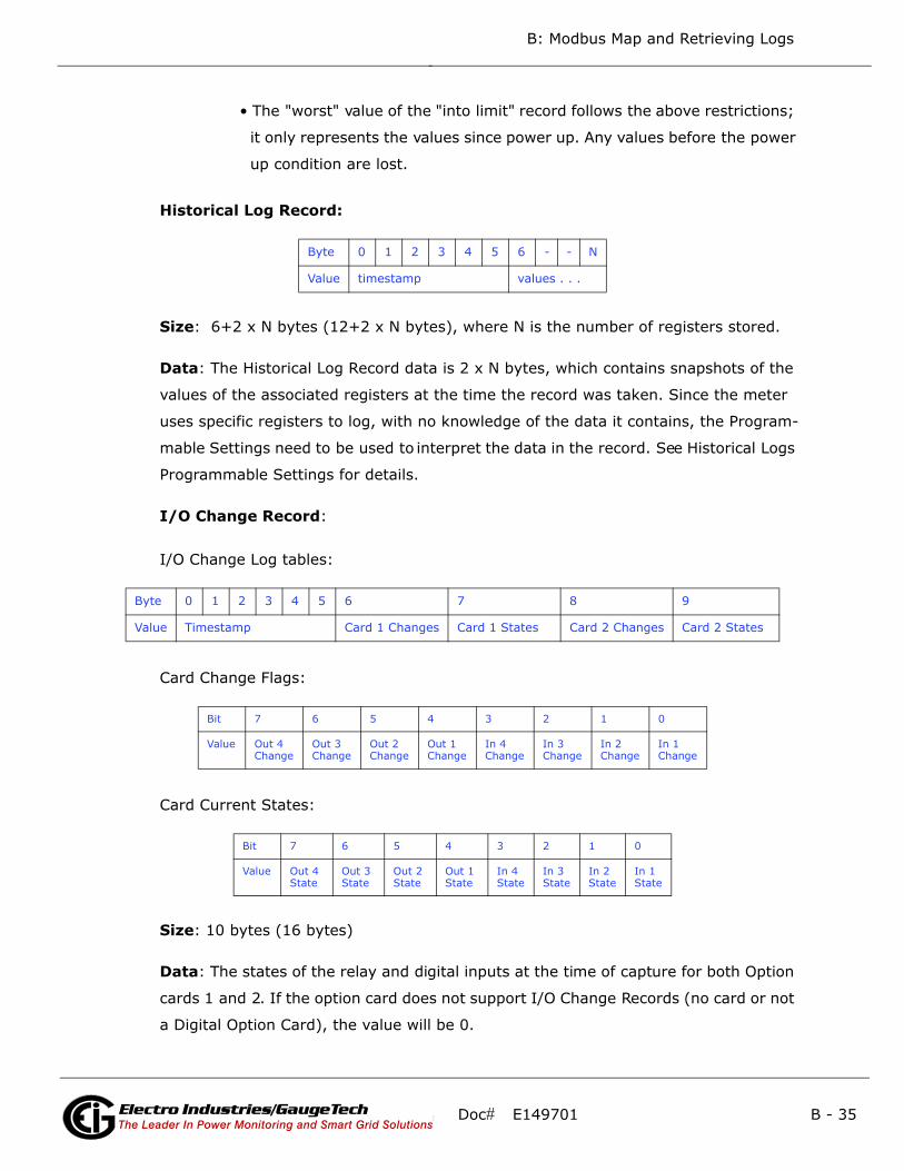
I/O Change Log (5)
I/O Change Log tables:
Card Change Flags:
Table 1:

#Electro Industries/GaugeTechThe Leader In Power Monitoring and Smart Grid SolutionsElectro Industries/GaugeTechThe Leader In Power Monitoring and Smart Grid Solutions
Card Current States:
B.5.3: Block Definitions
NOTES:
Historical Log Programmable Settings:

#Electro Industries/GaugeTechThe Leader In Power Monitoring and Smart Grid SolutionsElectro Industries/GaugeTechThe Leader In Power Monitoring and Smart Grid Solutions

#Electro Industries/GaugeTechThe Leader In Power Monitoring and Smart Grid SolutionsElectro Industries/GaugeTechThe Leader In Power Monitoring and Smart Grid Solutions
NOTE:

#Electro Industries/GaugeTechThe Leader In Power Monitoring and Smart Grid SolutionsElectro Industries/GaugeTechThe Leader In Power Monitoring and Smart Grid Solutions
NOTE:
Register Items Descriptors

#Electro Industries/GaugeTechThe Leader In Power Monitoring and Smart Grid SolutionsElectro Industries/GaugeTechThe Leader In Power Monitoring and Smart Grid Solutions
NOTE:
Log Base Address

#Electro Industries/GaugeTechThe Leader In Power Monitoring and Smart Grid SolutionsElectro Industries/GaugeTechThe Leader In Power Monitoring and Smart Grid Solutions
NOTE:
NOTE:
NOTES:

#Electro Industries/GaugeTechThe Leader In Power Monitoring and Smart Grid SolutionsElectro Industries/GaugeTechThe Leader In Power Monitoring and Smart Grid Solutions
Session Com Port
Log Retrieval Header:

#Electro Industries/GaugeTechThe Leader In Power Monitoring and Smart Grid SolutionsElectro Industries/GaugeTechThe Leader In Power Monitoring and Smart Grid Solutions

#Electro Industries/GaugeTechThe Leader In Power Monitoring and Smart Grid SolutionsElectro Industries/GaugeTechThe Leader In Power Monitoring and Smart Grid Solutions
#Electro Industries/GaugeTechThe Leader In Power Monitoring and Smart Grid SolutionsElectro Industries/GaugeTechThe Leader In Power Monitoring and Smart Grid Solutions
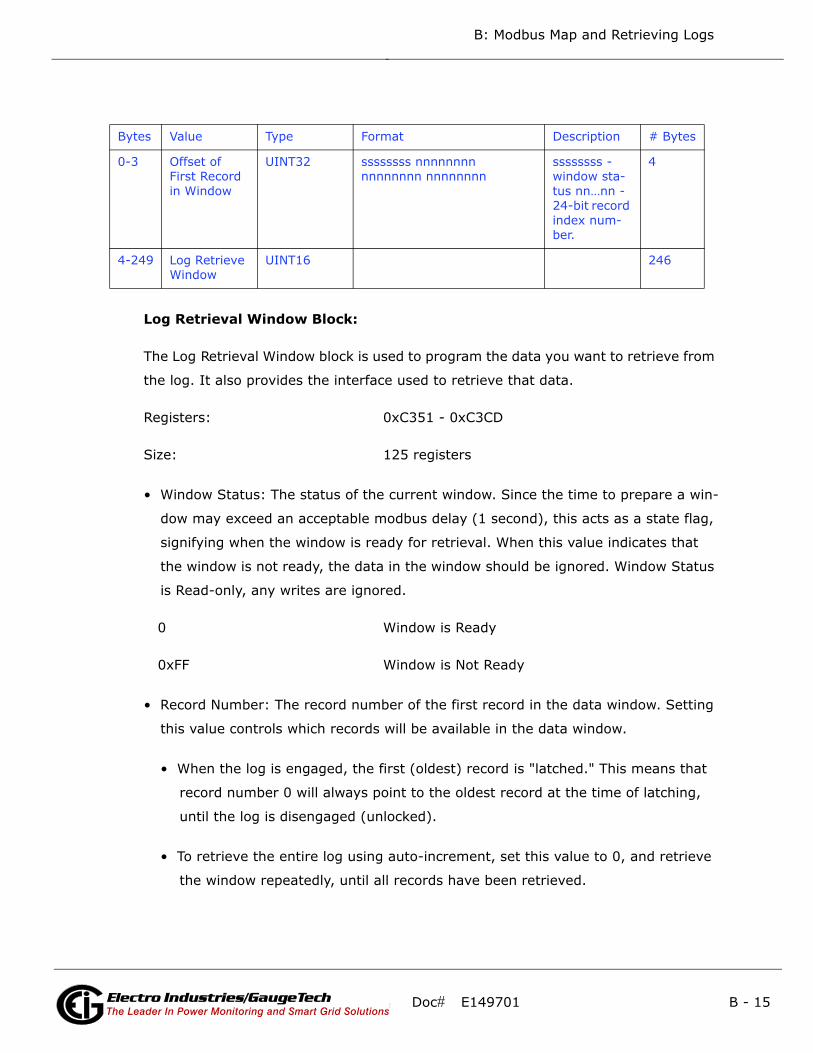
Log Retrieval Window Block:
#Electro Industries/GaugeTechThe Leader In Power Monitoring and Smart Grid SolutionsElectro Industries/GaugeTechThe Leader In Power Monitoring and Smart Grid Solutions
NOTES:
B.5.4: Log Retrieval
B.5.4.1: Auto-Increment
B.5.4.2: Modbus Function Code 0x23
QUERY
#Electro Industries/GaugeTechThe Leader In Power Monitoring and Smart Grid SolutionsElectro Industries/GaugeTechThe Leader In Power Monitoring and Smart Grid Solutions
NOTES:
IMPORTANT!
B.5.4.3: Log Retrieval Procedure
Scope
NOTES:

#Electro Industries/GaugeTechThe Leader In Power Monitoring and Smart Grid SolutionsElectro Industries/GaugeTechThe Leader In Power Monitoring and Smart Grid Solutions

#Electro Industries/GaugeTechThe Leader In Power Monitoring and Smart Grid SolutionsElectro Industries/GaugeTechThe Leader In Power Monitoring and Smart Grid Solutions
NOTES:

#Electro Industries/GaugeTechThe Leader In Power Monitoring and Smart Grid SolutionsElectro Industries/GaugeTechThe Leader In Power Monitoring and Smart Grid Solutions
B.5.4.4: Log Retrieval Example

#Electro Industries/GaugeTechThe Leader In Power Monitoring and Smart Grid SolutionsElectro Industries/GaugeTechThe Leader In Power Monitoring and Smart Grid Solutions
Send:
Command
Receive
Data
NOTE
Send
Command
Data

#Electro Industries/GaugeTechThe Leader In Power Monitoring and Smart Grid SolutionsElectro Industries/GaugeTechThe Leader In Power Monitoring and Smart Grid Solutions
Receive
NOTE
Send
Command
Receive
Data
NOTE
#Electro Industries/GaugeTechThe Leader In Power Monitoring and Smart Grid SolutionsElectro Industries/GaugeTechThe Leader In Power Monitoring and Smart Grid Solutions
Send
Command
Data
Receive
NOTES

#Electro Industries/GaugeTechThe Leader In Power Monitoring and Smart Grid SolutionsElectro Industries/GaugeTechThe Leader In Power Monitoring and Smart Grid Solutions
Send
Command
Receive
Data
NOTE:

#Electro Industries/GaugeTechThe Leader In Power Monitoring and Smart Grid SolutionsElectro Industries/GaugeTechThe Leader In Power Monitoring and Smart Grid Solutions
NOTES
NOTES
Send
Command
Data

#Electro Industries/GaugeTechThe Leader In Power Monitoring and Smart Grid SolutionsElectro Industries/GaugeTechThe Leader In Power Monitoring and Smart Grid Solutions
Receive
NOTES
NOTES
NOTES

#Electro Industries/GaugeTechThe Leader In Power Monitoring and Smart Grid SolutionsElectro Industries/GaugeTechThe Leader In Power Monitoring and Smart Grid Solutions
NOTES
Send
Command

#Electro Industries/GaugeTechThe Leader In Power Monitoring and Smart Grid SolutionsElectro Industries/GaugeTechThe Leader In Power Monitoring and Smart Grid Solutions
Data
Receive
NOTES
B.5.5: Log Record Interpretation
System Event Record:
Size
Data

#Electro Industries/GaugeTechThe Leader In Power Monitoring and Smart Grid SolutionsElectro Industries/GaugeTechThe Leader In Power Monitoring and Smart Grid Solutions
NOTE

#Electro Industries/GaugeTechThe Leader In Power Monitoring and Smart Grid SolutionsElectro Industries/GaugeTechThe Leader In Power Monitoring and Smart Grid Solutions

#Electro Industries/GaugeTechThe Leader In Power Monitoring and Smart Grid SolutionsElectro Industries/GaugeTechThe Leader In Power Monitoring and Smart Grid Solutions
NOTES
Alarm Record
Size
Data

#Electro Industries/GaugeTechThe Leader In Power Monitoring and Smart Grid SolutionsElectro Industries/GaugeTechThe Leader In Power Monitoring and Smart Grid Solutions
Interpretation of Alarm Data:

#Electro Industries/GaugeTechThe Leader In Power Monitoring and Smart Grid SolutionsElectro Industries/GaugeTechThe Leader In Power Monitoring and Smart Grid Solutions

#Electro Industries/GaugeTechThe Leader In Power Monitoring and Smart Grid SolutionsElectro Industries/GaugeTechThe Leader In Power Monitoring and Smart Grid Solutions
NOTES
#Electro Industries/GaugeTechThe Leader In Power Monitoring and Smart Grid SolutionsElectro Industries/GaugeTechThe Leader In Power Monitoring and Smart Grid Solutions
Historical Log Record:
Size
Data
I/O Change Record
Size
Data
#Electro Industries/GaugeTechThe Leader In Power Monitoring and Smart Grid SolutionsElectro Industries/GaugeTechThe Leader In Power Monitoring and Smart Grid Solutions
NOTES
B.5.6: Examples
Log Retrieval Section:
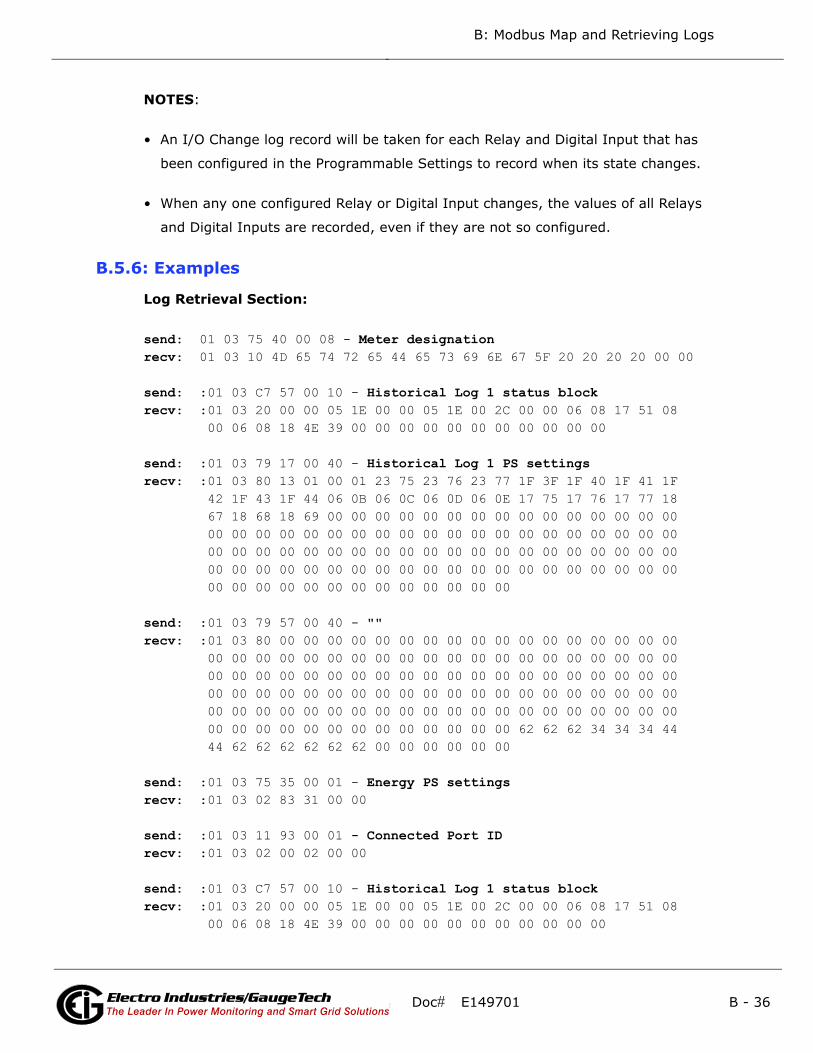
send: 01 03 75 40 00 08 - Meter designation
recv: 01 03 10 4D 65 74 72 65 44 65 73 69 6E 67 5F 20 20 20 20 00 00
send: :01 03 C7 57 00 10 - Historical Log 1 status block
recv: :01 03 20 00 00 05 1E 00 00 05 1E 00 2C 00 00 06 08 17 51 08
00 06 08 18 4E 39 00 00 00 00 00 00 00 00 00 00 00
send: :01 03 79 17 00 40 - Historical Log 1 PS settings
recv: :01 03 80 13 01 00 01 23 75 23 76 23 77 1F 3F 1F 40 1F 41 1F
42 1F 43 1F 44 06 0B 06 0C 06 0D 06 0E 17 75 17 76 17 77 18
67 18 68 18 69 00 00 00 00 00 00 00 00 00 00 00 00 00 00 00
00 00 00 00 00 00 00 00 00 00 00 00 00 00 00 00 00 00 00 00
00 00 00 00 00 00 00 00 00 00 00 00 00 00 00 00 00 00 00 00
00 00 00 00 00 00 00 00 00 00 00 00 00 00 00 00 00 00 00 00
00 00 00 00 00 00 00 00 00 00 00 00 00
send: :01 03 79 57 00 40 - ""
recv: :01 03 80 00 00 00 00 00 00 00 00 00 00 00 00 00 00 00 00 00
00 00 00 00 00 00 00 00 00 00 00 00 00 00 00 00 00 00 00 00
00 00 00 00 00 00 00 00 00 00 00 00 00 00 00 00 00 00 00 00
00 00 00 00 00 00 00 00 00 00 00 00 00 00 00 00 00 00 00 00
00 00 00 00 00 00 00 00 00 00 00 00 00 00 00 00 00 00 00 00
00 00 00 00 00 00 00 00 00 00 00 00 00 62 62 62 34 34 34 44
44 62 62 62 62 62 62 00 00 00 00 00 00
send: :01 03 75 35 00 01 - Energy PS settings
recv: :01 03 02 83 31 00 00
send: :01 03 11 93 00 01 - Connected Port ID
recv: :01 03 02 00 02 00 00
send: :01 03 C7 57 00 10 - Historical Log 1 status block
recv: :01 03 20 00 00 05 1E 00 00 05 1E 00 2C 00 00 06 08 17 51 08
00 06 08 18 4E 39 00 00 00 00 00 00 00 00 00 00 00

#Electro Industries/GaugeTechThe Leader In Power Monitoring and Smart Grid SolutionsElectro Industries/GaugeTechThe Leader In Power Monitoring and Smart Grid Solutions
send: :01 03 C3 4F 00 01 - Log Retrieval header
recv: :01 03 02 FF FF 00 00
send: :01 10 C3 4F 00 04 08 02 80 05 01 00 00 00 00 - Engage the log
recv: :01 10 C3 4F 00 04
send: :01 03 C7 57 00 10 - Historical Log 1 status block
recv: :01 03 20 00 00 05 1E 00 00 05 1E 00 2C 00 02 06 08 17 51 08
00 06 08 18 4E 39 00 00 00 00 00 00 00 00 00 00 00
send: :01 10 C3 51 00 02 04 00 00 00 00 - Set the retrieval index
recv: :01 10 C3 51 00 02
send: :01 03 C3 51 00 40 - Read first half of window
recv: :01 03 80 00 00 00 00 06 08 17 51 08 00 00 19 00 2F 27 0F 00
00 00 00 00 00 00 00 00 00 00 00 00 00 00 00 00 00 00 00 03
E8 00 01 00 05 00 00 00 00 00 00 06 08 17 51 09 00 00 19 00
2F 27 0F 00 00 00 00 00 00 00 00 00 00 00 00 00 00 00 00 00
00 00 00 03 E8 00 01 00 04 00 00 00 00 00 00 06 08 17 51 0A
00 00 19 00 2F 27 0F 00 00 00 00 00 00 00 00 00 00 00 00 00
00 00 00 00 00 00 00 03 E8 00 00 00 00
send: :01 03 C3 91 00 30 - Read second half of window
recv: :01 03 60 00 05 00 00 00 00 00 00 06 08 17 51 0B 00 00 19 00
2F 27 0F 00 00 00 00 00 00 00 00 00 00 00 00 00 00 00 00 00
00 00 00 03 E8 00 01 00 04 00 00 00 00 00 00 06 08 17 51 0C
00 00 19 00 2F 27 0F 00 00 00 00 00 00 00 00 00 00 00 00 00
00 00 00 00 00 00 00 03 E8 00 01 00 04 00 00 00 00 00 00 00
00
send: :01 03 C3 51 00 40 - Read first half of last window
recv: :01 03 80 00 00 05 19 06 08 18 4E 35 00 00 19 00 2F 27 0F 00
00 00 00 00 00 00 00 00 00 00 00 00 00 00 00 00 00 00 00 03
E8 00 01 00 04 00 00 00 00 00 00 06 08 18 4E 36 00 00 19 00
2F 27 0F 00 00 00 00 00 00 00 00 00 00 00 00 00 00 00 00 00
00 00 00 03 E8 00 01 00 04 00 00 00 00 00 00 06 08 18 4E 37
00 00 19 00 2F 27 0F 00 00 00 00 00 00 00 00 00 00 00 00 00
00 00 00 00 00 00 00 03 E8 00 00 00 00
send: :01 03 C3 91 00 30 - Read second half of last window
recv: :01 03 60 00 05 00 00 00 00 00 00 06 08 18 4E 38 00 00 19 00
2F 27 0F 00 00 00 00 00 00 00 00 00 00 00 00 00 00 00 00 00
00 00 00 03 E8 00 01 00 04 00 00 00 00 00 00 06 08 18 4E 39
00 00 19 00 2F 27 0F 00 00 00 00 00 00 00 00 00 00 00 00 00
00 00 00 00 00 00 00 03 E8 00 00 00 05 00 00 00 00 00 00 00
00
send: :01 06 C3 4F 00 00 - Disengage the log

#Electro Industries/GaugeTechThe Leader In Power Monitoring and Smart Grid SolutionsElectro Industries/GaugeTechThe Leader In Power Monitoring and Smart Grid Solutions
recv: :01 06 C3 4F 00 00
Sample Historical Log 1 Record:
13|01|00 01|23 75|23 76|23 77|1F 3F 1F 40|1F 41
1F 42|1F 43 1F 44|06 0B 06 0C|06 0D 06 0E|17 75|
17 76|17 77|18 67|18 68|18 69|00 00 . . . . . .
62 62 62 34 34 34 44 44 62 62 62 62 62 62 . . .
These are the These are the These are the Descriptions:
Item Values: Type and Size:
13 - # registers
01 - # sectors
01 - interval
23 75 6 2 - (SINT 2 byte) Volts A THD Maximum
23 76 6 2 - (SINT 2 byte) Volts B THD Maximum
23 77 6 2 - (SINT 2 byte) Volts C THD Maximum
1F 3F 1F 40 3 4 - (Float 4 byte) Volts A Minimum
1F 41 1F 42 3 4 - (Float 4 byte) Volts B Minimum
1F 43 1F 44 3 4 - (Float 4 byte) Volts C Minimum
06 0B 06 0C 4 4 - (Energy 4 byte) VARhr Negative Phase A
06 0D 06 0E 4 4 - (Energy 4 byte) VARhr Negative Phase B
17 75 6 2 - (SINT 2 byte) Volts A 1st Harmonic
Magnitude
17 76 6 2 - (SINT 2 byte) Volts A 2nd Harmonic
Magnitude
17 77 6 2 - (SINT 2 byte) Volts A 3rd Harmonic
Magnitude
18 67 6 2 - (SINT 2 byte) Ib 3rd Harmonic Magnitude
18 68 6 2 - (SINT 2 byte) Ib 4th Harmonic Magnitude
18 69 6 2 - (SINT 2 byte) Ib 5th Harmonic Magnitude
Sample Record
06 08 17 51 08 00|00 19|00 2F|27 0F|00 00 00 00|00
00 00 00|00 00 00 00|00 00 00 00|00 00 00 00|03 E8|
00 01|00 05|00 00|00 00|00 00 . . .
11 08 17 51 08 00 - August 23, 2011 17:08:00
00 19 - 2.5%
00 2F - 4.7%
27 0F - 999.9% (indicates the value isn’t valid)
00 00 00 00 - 0

#Electro Industries/GaugeTechThe Leader In Power Monitoring and Smart Grid SolutionsElectro Industries/GaugeTechThe Leader In Power Monitoring and Smart Grid Solutions
00 00 00 00 - 0
00 00 00 00 - 0
00 00 00 00 - 0
00 00 00 00 - 0
03 E8 - 100.0% (Fundamental)
00 01 - 0.1%
00 05 - 0.5%
00 00 - 0.0%
00 00 - 0.0%
00 00 - 0.0%
B.6: Important Note Concerning the Shark ® 200 Meter's Modbus Map
B.6.1: Hex Representation
B.6.2: Decimal Representation

#Electro Industries/GaugeTechThe Leader In Power Monitoring and Smart Grid SolutionsElectro Industries/GaugeTechThe Leader In Power Monitoring and Smart Grid Solutions
B.7: Modbus Register Map (MM-1 to MM-40)

B:
Modbus M
ap a
nd R
etr
ievin
g L
ogs
Doc#
E149701
MM
-1Electro Industries/GaugeTech
The Leader In Power Monitoring and Smart Grid Solutions
De
sc
rip
tio
n (
No
te 1
)F
orm
at
Ra
ng
e (
No
te 6
)U
nit
s o
r R
es
olu
tio
nC
om
me
nts
# R
eg
read
-on
ly
0000
-0007
1-
8M
ete
r N
am
eA
SC
II16 c
har
none
8
0008
-000F
9-
16
Mete
r S
erial N
um
ber
AS
CII
16 c
har
none
8
0010
-0010
17
-17
Mete
r T
ype
UIN
T16
bit-m
apped
------st -----vvv
t =
tra
nsducer
model (1
=yes, 0=
no),
s=
subm
ete
r m
odel(1=
yes,0
=no),
vvv =
V-s
witch:
V1 =
sta
ndard
200,
V2 =
V1 p
lus loggin
g,
V3 =
V2 p
lus T
HD
,
V4 =
V3 p
lus r
ela
ys,
V5 =
V4 p
lus w
avefo
rm c
aptu
re u
p to 6
4 s
am
ple
s/c
ycle
and 3
Meg,
V6 =
V4 p
lus w
avefo
rm c
aptu
re u
p to 5
12 s
am
ple
s/c
ycle
and 4
Meg
1
0011
-0012
18
-19
Firm
ware
Vers
ion
AS
CII
4 c
har
none
2
0013
-0013
20
-20
Map V
ers
ion
UIN
T16
0 to 6
5535
none
1
0014
-0014
21
-21
Mete
r C
onfigura
tion
UIN
T16
bit-m
apped
-----ccc --ffffff
ccc =
CT
denom
inato
r (1
or
5),
ffffff =
calib
ration fre
quency (
50 o
r 60)
1
0015
-0015
22
-22
AS
IC V
ers
ion
UIN
T16
0-6
5535
none
1
0016
-0017
23
-24
Boot F
irm
ware
Vers
ion
AS
CII
4 c
har
none
2
0018
-0018
25
-25
Option S
lot 1 U
sage
UIN
T16
bit-m
apped
sam
e a
s r
egis
ter
10000
(0x270F
)
1
0019
-0019
26
-26
Option S
lot 2 U
sage
UIN
T16
bit-m
apped
sam
e a
s r
egis
ter
11000
(0x2A
F7)
1
001A
-001D
27
-30
Mete
r T
ype N
am
eA
SC
II8 c
har
none
4
001E
-0026
31
-39
Reserv
ed
Reserv
ed
9
0027
-002E
40
-47
Reserv
ed
Reserv
ed
8
002F
-0115
48
-278
Reserv
ed
Reserv
ed
231
0116
-0130
279
-305
0131
-01F
3306
-500
Reserv
ed
Reserv
ed
194
01F
4-
0203
501
-516
Reserv
ed
Reserv
ed
16
Mo
db
us
Ad
dre
ss
He
xD
ec
ima
l
Fix
ed
Da
ta S
ec
tio
nId
en
tifi
cati
on
Blo
ck
Inte
ger
Readin
gs B
lock o
ccupie
s these r
egis
ters
, see b
elo
w

B:
Modbus M
ap a
nd R
etr
ievin
g L
ogs
Doc#
E149701
MM
-2Electro Industries/GaugeTech
The Leader In Power Monitoring and Smart Grid Solutions
De
sc
rip
tio
n (
No
te 1
)F
orm
at
Ra
ng
e (
No
te 6
)U
nit
s o
r R
es
olu
tio
nC
om
me
nts
# R
eg
Mo
db
us
Ad
dre
ss
He
xD
ec
ima
l
read
-on
ly
0116
-0116
279
-279
Volts A
-NU
INT
16
0 to 9
999
volts
1
0117
-0117
280
-280
Volts B
-NU
INT
16
0 to 9
999
volts
1
0118
-0118
281
-281
Volts C
-NU
INT
16
0 to 9
999
volts
1
0119
-0119
282
-282
Volts A
-BU
INT
16
0 to 9
999
volts
1
011A
-011A
283
-283
Volts B
-CU
INT
16
0 to 9
999
volts
1
011B
-011B
284
-284
Volts C
-AU
INT
16
0 to 9
999
volts
1
011C
-011C
285
-285
Am
ps A
UIN
T16
0 to 9
999
am
ps
1
011D
-011D
286
-286
Am
ps B
UIN
T16
0 to 9
999
am
ps
1
011E
-011E
287
-287
Am
ps C
UIN
T16
0 to 9
999
am
ps
1
011F
-011F
288
-288
Neutr
al C
urr
ent
UIN
T16
-9999 to
+9999
am
ps
1
0120
-0120
289
-289
Watts, 3-P
h tota
lS
INT
16
-9999 to
+9999
watts
1
0121
-0121
290
-290
VA
Rs, 3-P
h tota
lS
INT
16
-9999 to
+9999
VA
Rs
1
0122
-0122
291
-291
VA
s, 3-P
h tota
lU
INT
16
0 to +
9999
VA
s1
0123
-0123
292
-292
Pow
er
Facto
r, 3
-Ph tota
lS
INT
16
-1000 to
+1000
none
1
0124
-0124
293
-293
Fre
quency
UIN
T16
0 to 9
999
Hz
1
0125
-0125
294
-294
Watts, P
hase A
SIN
T16
-9999 M
to +
9999
watts
1
0126
-0126
295
-295
Watts, P
hase B
SIN
T16
-9999 M
to +
9999
watts
1
0127
-0127
296
-296
Watts, P
hase C
SIN
T16
-9999 M
to +
9999
watts
1
0128
-0128
297
-297
VA
Rs, P
hase A
SIN
T16
-9999 M
to +
9999 M
VA
Rs
1
0129
-0129
298
-298
VA
Rs, P
hase B
SIN
T16
-9999 M
to +
9999 M
VA
Rs
1
012A
-012A
299
-299
VA
Rs, P
hase C
SIN
T16
-9999 M
to +
9999 M
VA
Rs
1
012B
-012B
300
-300
VA
s, P
hase A
UIN
T16
0 to +
9999
VA
s1
012C
-012C
301
-301
VA
s, P
hase B
UIN
T16
0 to +
9999
VA
s1
012D
-012D
302
-302
VA
s, P
hase C
UIN
T16
0 to +
9999
VA
s1
012E
-012E
303
-303
Pow
er
Facto
r, P
hase A
SIN
T16
-1000 to
+1000
none
1
012F
-012F
304
-304
Pow
er
Facto
r, P
hase B
SIN
T16
-1000 to
+1000
none
1
0130
-0130
305
-305
Pow
er
Facto
r, P
hase C
SIN
T16
-1000 to
+1000
none
1
Blo
ck S
ize:
27
read
-on
ly
03E
7-
03E
81000
-1001
Volts A
-NF
LO
AT
0 to 9
999 M
volts
2
03E
9-
03E
A1002
-1003
Volts B
-NF
LO
AT
0 to 9
999 M
volts
2
03E
B-
03E
C1004
-1005
Volts C
-NF
LO
AT
0 to 9
999 M
volts
2
03E
D-
03E
E1006
-1007
Volts A
-BF
LO
AT
0 to 9
999 M
volts
2
03E
F-
03F
01008
-1009
Volts B
-CF
LO
AT
0 to 9
999 M
volts
2
03F
1-
03F
21010
-1011
Volts C
-AF
LO
AT
0 to 9
999 M
volts
2
03F
3-
03F
41012
-1013
Am
ps A
FLO
AT
0 to 9
999 M
am
ps
2
03F
5-
03F
61014
-1015
Am
ps B
FLO
AT
0 to 9
999 M
am
ps
2
03F
7-
03F
81016
-1017
Am
ps C
FLO
AT
0 to 9
999 M
am
ps
2
03F
9-
03F
A1018
-1019
Watts, 3-P
h tota
lF
LO
AT
-9999 M
to +
9999 M
watts
2
03F
B-
03F
C1020
-1021
VA
Rs, 3-P
h tota
lF
LO
AT
-9999 M
to +
9999 M
VA
Rs
2
03F
D-
03F
E1022
-1023
VA
s, 3-P
h tota
lF
LO
AT
-9999 M
to +
9999 M
VA
s2
03F
F-
0400
1024
-1025
Pow
er
Facto
r, 3
-Ph tota
lF
LO
AT
-1.0
0 to +
1.0
0none
2
0401
-0402
1026
-1027
Fre
quency
FLO
AT
0 to 6
5.0
0H
z2
0403
-0404
1028
-1029
Neutr
al C
urr
ent
FLO
AT
0 to 9
999 M
am
ps
2
Me
ter
Da
ta S
ec
tio
n (
No
te 2
)R
ead
ing
s B
lock (
In
teg
er
valu
es)
1.U
se the s
ettin
gs fro
m P
rogra
mm
able
settin
gs for
scale
and d
ecim
al poin
t lo
cation. (s
ee U
ser
Settin
gs F
lags)
2. P
er
phase p
ow
er
and P
F h
ave v
alu
es
only
for
WY
E h
ookup a
nd w
ill b
e
zero
for
all
oth
er
hookups.
3. If the r
eadin
g is 1
0000 that m
eans that th
e v
alu
e is o
ut
of ra
nge. P
lease a
dju
st th
e p
rogra
mm
able
settin
gs in
that case. T
he d
ispla
y w
ill a
lso s
how
'---
-' in case o
f over
range.
Pri
mary
Read
ing
s B
lock

B:
Modbus M
ap a
nd R
etr
ievin
g L
ogs
Doc#
E149701
MM
-3Electro Industries/GaugeTech
The Leader In Power Monitoring and Smart Grid Solutions
De
sc
rip
tio
n (
No
te 1
)F
orm
at
Ra
ng
e (
No
te 6
)U
nit
s o
r R
es
olu
tio
nC
om
me
nts
# R
eg
Mo
db
us
Ad
dre
ss
He
xD
ec
ima
l
0405
-0406
1030
-1031
Watts, P
hase A
FLO
AT
-9999 M
to +
9999 M
watts
2
0407
-0408
1032
-1033
Watts, P
hase B
FLO
AT
-9999 M
to +
9999 M
watts
2
0409
-040A
1034
-1035
Watts, P
hase C
FLO
AT
-9999 M
to +
9999 M
watts
2
040B
-040C
1036
-1037
VA
Rs, P
hase A
FLO
AT
-9999 M
to +
9999 M
VA
Rs
2
040D
-040E
1038
-1039
VA
Rs, P
hase B
FLO
AT
-9999 M
to +
9999 M
VA
Rs
2
040F
-0410
1040
-1041
VA
Rs, P
hase C
FLO
AT
-9999 M
to +
9999 M
VA
Rs
2
0411
-0412
1042
-1043
VA
s, P
hase A
FLO
AT
-9999 M
to +
9999 M
VA
s2
0413
-0414
1044
-1045
VA
s, P
hase B
FLO
AT
-9999 M
to +
9999 M
VA
s2
0415
-0416
1046
-1047
VA
s, P
hase C
FLO
AT
-9999 M
to +
9999 M
VA
s2
0417
-0418
1048
-1049
Pow
er
Facto
r, P
hase A
FLO
AT
-1.0
0 to +
1.0
0none
2
0419
-041A
1050
-1051
Pow
er
Facto
r, P
hase B
FLO
AT
-1.0
0 to +
1.0
0none
2
041B
-041C
1052
-1053
Pow
er
Facto
r, P
hase C
FLO
AT
-1.0
0 to +
1.0
0none
2
041D
-041E
1054
-1055
Sym
metr
ical C
om
ponent M
agnitude, 0 S
eq
FLO
AT
0 to 9
999 M
volts
2
041F
-0420
1056
-1057
Sym
metr
ical C
om
ponent M
agnitude, +
Seq
FLO
AT
0 to 9
999 M
volts
2
0421
-0422
1058
-1059
Sym
metr
ical C
om
ponent M
agnitude, -
Seq
FLO
AT
0 to 9
999 M
volts
2
0423
-0423
1060
-1060
Sym
metr
ical C
om
ponent P
hase, 0 S
eq
SIN
T16
-1800 to +
1800
0.1
degre
e1
0424
-0424
1061
-1061
Sym
metr
ical C
om
ponent P
hase, +
Seq
SIN
T16
-1800 to +
1800
0.1
degre
e1
0425
-0425
1062
-1062
Sym
metr
ical C
om
ponent P
hase, -
Seq
SIN
T16
-1800 to +
1800
0.1
degre
e1
0426
-0426
1063
-1063
Unbala
nce, 0 s
equence c
om
ponent
UIN
T16
0 to 6
5535
0.0
1%
1
0427
-0427
1064
-1064
Unbala
nce, -s
equence c
om
ponent
UIN
T16
0 to 6
5535
0.0
1%
1
0428
-0428
1065
-1065
Curr
ent U
nbala
nce
UIN
T16
0 to 2
0000
0.0
1%
1
Blo
ck S
ize:
66
read
-on
ly
05D
B -
05D
C1500
-1501
W-h
ours
, R
eceiv
ed
SIN
T32
0 to 9
9999999 o
r
0 to -
99999999
Wh p
er
energ
y form
at
2
05D
D-
05D
E1502
-1503
W-h
ours
, D
eliv
ere
dS
INT
32
0 to 9
9999999 o
r
0 to -
99999999
Wh p
er
energ
y form
at
2
05D
F-
05E
01504
-1505
W-h
ours
, N
et
SIN
T32
-99999999 to 9
9999999
Wh p
er
energ
y form
at
2
05E
1-
05E
21506
-1507
W-h
ours
, T
ota
lS
INT
32
0 to 9
9999999
Wh p
er
energ
y form
at
2
05E
3-
05E
41508
-1509
VA
R-h
ours
, P
ositiv
eS
INT
32
0 to 9
9999999
VA
Rh p
er
energ
y form
at
2
05E
5-
05E
61510
-1511
VA
R-h
ours
, N
egative
SIN
T32
0 to -
99999999
VA
Rh p
er
energ
y form
at
2
05E
7-
05E
81512
-1513
VA
R-h
ours
, N
et
SIN
T32
-99999999 to 9
9999999
VA
Rh p
er
energ
y form
at
2
05E
9-
05E
A1514
-1515
VA
R-h
ours
, T
ota
lS
INT
32
0 to 9
9999999
VA
Rh p
er
energ
y form
at
2
05E
B-
05E
C1516
-1517
VA
-hours
, T
ota
lS
INT
32
0 to 9
9999999
VA
h p
er
energ
y form
at
2
05E
D-
05E
E1518
-1519
W-h
ours
, R
eceiv
ed, P
hase A
SIN
T32
0 to 9
9999999 o
r
0 to -
99999999
Wh p
er
energ
y form
at
2
05E
F-
05F
01520
-1521
W-h
ours
, R
eceiv
ed, P
hase B
SIN
T32
0 to 9
9999999 o
r
0 to -
99999999
Wh p
er
energ
y form
at
2
05F
1-
05F
21522
-1523
W-h
ours
, R
eceiv
ed, P
hase C
SIN
T32
0 to 9
9999999 o
r
0 to -
99999999
Wh p
er
energ
y form
at
2
05F
3-
05F
41524
-1525
W-h
ours
, D
eliv
ere
d, P
hase A
SIN
T32
0 to 9
9999999 o
r
0 to -
99999999
Wh p
er
energ
y form
at
2
05F
5-
05F
61526
-1527
W-h
ours
, D
eliv
ere
d, P
hase B
SIN
T32
0 to 9
9999999 o
r
0 to -
99999999
Wh p
er
energ
y form
at
2
05F
7-
05F
81528
-1529
W-h
ours
, D
eliv
ere
d, P
hase C
SIN
T32
0 to 9
9999999 o
r
0 to -
99999999
Wh p
er
energ
y form
at
2
05F
9-
05F
A1530
-1531
W-h
ours
, N
et, P
hase A
SIN
T32
-99999999 to 9
9999999
Wh p
er
energ
y form
at
2
05F
B-
05F
C1532
-1533
W-h
ours
, N
et, P
hase B
SIN
T32
-99999999 to 9
9999999
Wh p
er
energ
y form
at
2
05F
D-
05F
E1534
-1535
W-h
ours
, N
et, P
hase C
SIN
T32
-99999999 to 9
9999999
Wh p
er
energ
y form
at
2
05F
F-
0600
1536
-1537
W-h
ours
, T
ota
l, P
hase A
SIN
T32
0 to 9
9999999
Wh p
er
energ
y form
at
2
0601
-0602
1538
-1539
W-h
ours
, T
ota
l, P
hase B
SIN
T32
0 to 9
9999999
Wh p
er
energ
y form
at
2
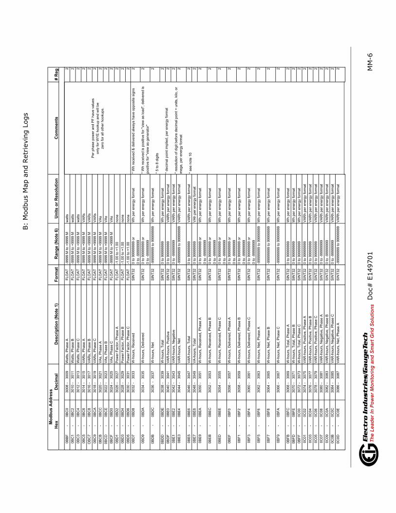
Per
phase p
ow
er
and P
F h
ave v
alu
es
only
for
WY
E h
ookup a
nd w
ill b
e
zero
for
all
oth
er
hookups.
Voltage u
nbala
nce p
er
IEC
6100-4
.30
Valu
es a
pply
only
to W
YE
hookup a
nd
will
be z
ero
for
all
oth
er
hookups.
Pri
mary
En
erg
y B
lock
* W
h r
eceiv
ed &
deliv
ere
d a
lways h
ave o
pposite s
igns
* W
h r
eceiv
ed is p
ositiv
e for
"vie
w a
s load",
deliv
ere
d is
positiv
e for
"vie
w a
s g
enera
tor"
* 5 to 8
dig
its
* decim
al poin
t im
plie
d, per
energ
y form
at
* re
solu
tion o
f dig
it b
efo
re d
ecim
al poin
t =
units, kilo
, or
mega, per
energ
y form
at
* see n
ote
10

B:
Modbus M
ap a
nd R
etr
ievin
g L
ogs
Doc#
E149701
MM
-4Electro Industries/GaugeTech
The Leader In Power Monitoring and Smart Grid Solutions
De
sc
rip
tio
n (
No
te 1
)F
orm
at
Ra
ng
e (
No
te 6
)U
nit
s o
r R
es
olu
tio
nC
om
me
nts
# R
eg
Mo
db
us
Ad
dre
ss
He
xD
ec
ima
l
0603
-0604
1540
-1541
W-h
ours
, T
ota
l, P
hase C
SIN
T32
0 to 9
9999999
Wh p
er
energ
y form
at
2
0605
-0606
1542
-1543
VA
R-h
ours
, P
ositiv
e, P
hase A
SIN
T32
0 to 9
9999999
VA
Rh p
er
energ
y form
at
2
0607
-0608
1544
-1545
VA
R-h
ours
, P
ositiv
e, P
hase B
SIN
T32
0 to 9
9999999
VA
Rh p
er
energ
y form
at
2
0609
-060A
1546
-1547
VA
R-h
ours
, P
ositiv
e, P
hase C
SIN
T32
0 to 9
9999999
VA
Rh p
er
energ
y form
at
2
060B
-060C
1548
-1549
VA
R-h
ours
, N
egative, P
hase A
SIN
T32
0 to -
99999999
VA
Rh p
er
energ
y form
at
2
060D
-060E
1550
-1551
VA
R-h
ours
, N
egative, P
hase B
SIN
T32
0 to -
99999999
VA
Rh p
er
energ
y form
at
2
060F
-0610
1552
-1553
VA
R-h
ours
, N
egative, P
hase C
SIN
T32
0 to -
99999999
VA
Rh p
er
energ
y form
at
2
0611
-0612
1554
-1555
VA
R-h
ours
, N
et, P
hase A
SIN
T32
-99999999 to 9
9999999
VA
Rh p
er
energ
y form
at
2
0613
-0614
1556
-1557
VA
R-h
ours
, N
et, P
hase B
SIN
T32
-99999999 to 9
9999999
VA
Rh p
er
energ
y form
at
2
0615
-0616
1558
-1559
VA
R-h
ours
, N
et, P
hase C
SIN
T32
-99999999 to 9
9999999
VA
Rh p
er
energ
y form
at
2
0617
-0618
1560
-1561
VA
R-h
ours
, T
ota
l, P
hase A
SIN
T32
0 to 9
9999999
VA
Rh p
er
energ
y form
at
2
0619
-061A
1562
-1563
VA
R-h
ours
, T
ota
l, P
hase B
SIN
T32
0 to 9
9999999
VA
Rh p
er
energ
y form
at
2
061B
-061C
1564
-1565
VA
R-h
ours
, T
ota
l, P
hase C
SIN
T32
0 to 9
9999999
VA
Rh p
er
energ
y form
at
2
061D
-061E
1566
-1567
VA
-hours
, P
hase A
SIN
T32
0 to 9
9999999
VA
h p
er
energ
y form
at
2
061F
-0620
1568
-1569
VA
-hours
, P
hase B
SIN
T32
0 to 9
9999999
VA
h p
er
energ
y form
at
2
0621
-0622
1570
-1571
VA
-hours
, P
hase C
SIN
T32
0 to 9
9999999
VA
h p
er
energ
y form
at
2
0623
-0624
1572
-1573
W-h
ours
, R
eceiv
ed, ro
llover
count
UIN
T32
0 to 4
,294,9
67,2
94
2
0625
-0626
1574
-1575
W-h
ours
, D
eliv
ere
d, ro
llover
count
UIN
T32
0 to 4
,294,9
67,2
94
2
0627
-0628
1576
-1577
VA
R-h
ours
, P
ositiv
e, ro
llover
count
UIN
T32
0 to 4
,294,9
67,2
94
2
0629
-062A
1578
-1579
VA
R-h
ours
, N
egative, ro
llover
count
UIN
T32
0 to 4
,294,9
67,2
94
2
062B
-062C
1580
-1581
VA
-hours
, ro
llover
count
UIN
T32
0 to 4
,294,9
67,2
94
2
062D
-062E
1582
-1583
W-h
ours
in the Inte
rval, R
eceiv
ed
SIN
T32
0 to 9
9999999 o
r
0 to -
99999999
Wh p
er
energ
y form
at
2
062F
-0630
1584
-1585
W-h
ours
in the Inte
rval, D
eliv
ere
dS
INT
32
0 to 9
9999999 o
r
0 to -
99999999
Wh p
er
energ
y form
at
2
0631
-0632
1586
-1587
VA
R-h
ours
in the Inte
rval, P
ositiv
eS
INT
32
0 to 9
9999999
VA
Rh p
er
energ
y form
at
2
0633
-0634
1588
-1589
VA
R-h
ours
in the Inte
rval, N
egative
SIN
T32
0 to -
99999999
VA
Rh p
er
energ
y form
at
2
0635
-0636
1590
-1591
VA
-hours
in the Inte
rval, T
ota
lS
INT
32
0 to 9
9999999
VA
h p
er
energ
y form
at
2
0637
-0638
1592
-1593
W-h
ours
in the Inte
rval, R
eceiv
ed, P
hase A
SIN
T32
0 to 9
9999999 o
r
0 to -
99999999
Wh p
er
energ
y form
at
2
0639
-063A
1594
-1595
W-h
ours
in the Inte
rval, R
eceiv
ed, P
hase B
SIN
T32
0 to 9
9999999 o
r
0 to -
99999999
Wh p
er
energ
y form
at
2
063B
-063C
1596
-1597
W-h
ours
in the Inte
rval, R
eceiv
ed, P
hase C
SIN
T32
0 to 9
9999999 o
r
0 to -
99999999
Wh p
er
energ
y form
at
2
063D
-063E
1598
-1599
W-h
ours
in the Inte
rval, D
eliv
ere
d, P
hase A
SIN
T32
0 to 9
9999999 o
r
0 to -
99999999
Wh p
er
energ
y form
at
2
063F
-0640
1600
-1601
W-h
ours
in the Inte
rval, D
eliv
ere
d, P
hase B
SIN
T32
0 to 9
9999999 o
r
0 to -
99999999
Wh p
er
energ
y form
at
2
0641
-0642
1602
-1603
W-h
ours
in the Inte
rval, D
eliv
ere
d, P
hase C
SIN
T32
0 to 9
9999999 o
r
0 to -
99999999
Wh p
er
energ
y form
at
2
0643
-0644
1604
-1605
VA
R-h
ours
in the Inte
rval, P
ositiv
e, P
hase A
SIN
T32
0 to 9
9999999
VA
Rh p
er
energ
y form
at
2
0645
-0646
1606
-1607
VA
R-h
ours
in the Inte
rval, P
ositiv
e, P
hase B
SIN
T32
0 to 9
9999999
VA
Rh p
er
energ
y form
at
2
0647
-0648
1608
-1609
VA
R-h
ours
in the Inte
rval, P
ositiv
e, P
hase C
SIN
T32
0 to 9
9999999
VA
Rh p
er
energ
y form
at
2
0649
-064A
1610
-1611
VA
R-h
ours
in the Inte
rval, N
egative, P
hase A
SIN
T32
0 to -
99999999
VA
Rh p
er
energ
y form
at
2
064B
-064C
1612
-1613
VA
R-h
ours
in the Inte
rval, N
egative, P
hase B
SIN
T32
0 to -
99999999
VA
Rh p
er
energ
y form
at
2
063D
-064E
1614
-1615
VA
R-h
ours
in the Inte
rval, N
egative, P
hase C
SIN
T32
0 to -
99999999
VA
Rh p
er
energ
y form
at
2
064F
-0650
1616
-1617
VA
-hours
in the Inte
rval, P
hase A
SIN
T32
0 to 9
9999999
VA
h p
er
energ
y form
at
2
0651
-0652
1618
-1619
VA
-hours
in the Inte
rval, P
hase B
SIN
T32
0 to 9
9999999
VA
h p
er
energ
y form
at
2
0653
-0654
1620
-1621
VA
-hours
in the Inte
rval, P
hase C
SIN
T32
0 to 9
9999999
VA
h p
er
energ
y form
at
2
Blo
ck S
ize:
122
These r
egis
ters
count th
e n
um
ber
of tim
es their
corr
espondin
g e
nerg
y a
ccum
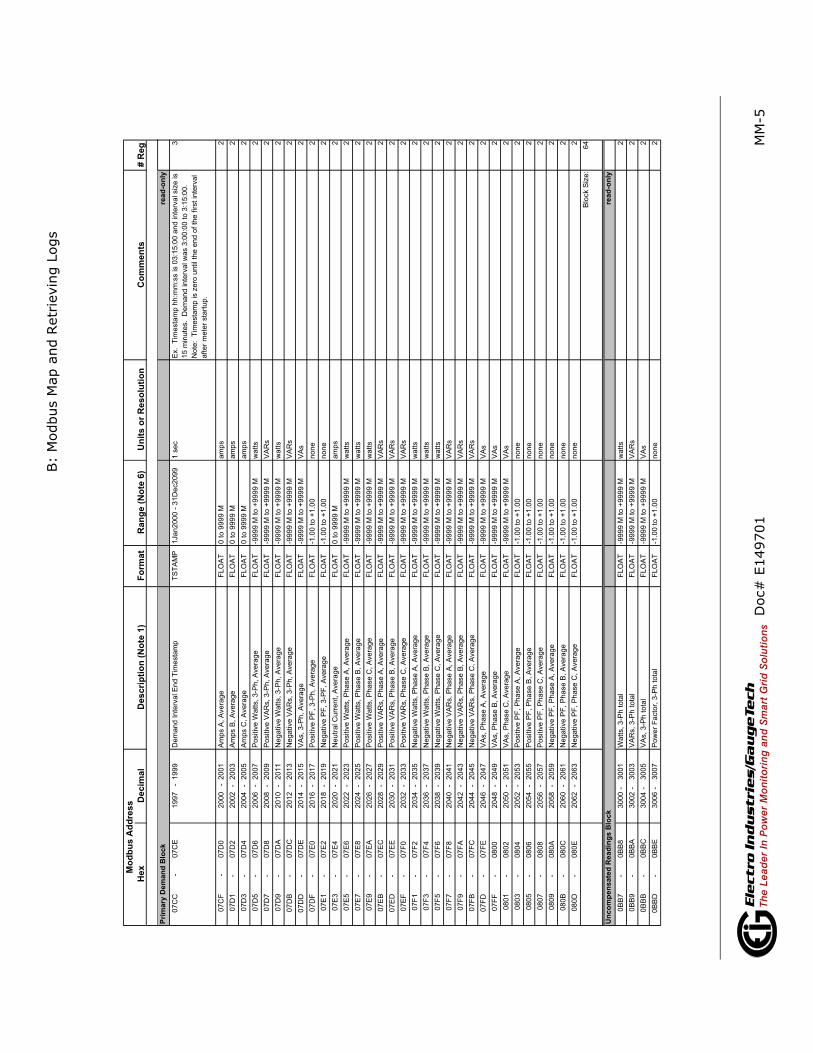
ula
tors
have w
rapped fro
m
+m
ax to 0
. T
hey a
re r
eset w
hen e
nerg
y is r
eset.
* W
h r
eceiv
ed &
deliv
ere
d a
lways h
ave o
pposite s
igns
* W
h r
eceiv
ed is p
ositiv
e for
"vie
w a
s load"
, deliv
ere
d is
positiv
e for
"vie
w a
s g
enera
tor"
* 5 to 8
dig
its
* decim
al poin
t im
plie
d, per
energ
y form
at
* re
solu
tion o
f dig
it b
efo
re d
ecim
al poin
t =
units, kilo
, or
mega, per
energ
y form
at
* see n
ote
10
B:
Modbus M
ap a
nd R
etr
ievin
g L
ogs
Doc#
E149701
MM
-5Electro Industries/GaugeTech
The Leader In Power Monitoring and Smart Grid Solutions
De
sc
rip
tio
n (
No
te 1
)F
orm
at
Ra
ng
e (
No
te 6
)U
nit
s o
r R
es
olu
tio
nC
om
me
nts
# R
eg
Mo
db
us
Ad
dre
ss
He
xD
ec
ima
l
read
-on
ly
07C
C -
07C
E1997
-1999
Dem
and Inte
rval E
nd T
imesta
mp
TS
TA
MP
1Jan2000 -
31D
ec2099
1 s
ec
Ex. T
imesta
mp h
h:m
m:s
s is 0
3:1
5:0
0 a
nd inte
rva
l siz
e is
15 m
inute
s. D
em
and inte
rval w
as 3
:00:0
0 to 3
:15:0
0.
Note
: T
imesta
mp is z
ero
until th
e e
nd o
f th
e first in
terv
al
after
mete
r sta
rtup.
3
07C
F -
07D
02000
-2001
Am
ps A
, A
vera
ge
FLO
AT
0 to 9
999 M
am
ps
2
07D
1-
07D
22002
-2003
Am
ps B
, A
vera
ge
FLO
AT
0 to 9
999 M
am
ps
2
07D
3-
07D
42004
-2005
Am
ps C
, A
vera
ge
FLO
AT
0 to 9
999 M
am
ps
2
07D
5-
07D
62006
-2007
Positiv
e W
atts, 3-P
h, A
vera
ge
FLO
AT
-9999 M
to +
9999 M
watts
2
07D
7-
07D
82008
-2009
Positiv
e V
AR
s, 3-P
h, A
vera
ge
FLO
AT
-9999 M
to +
9999 M
VA
Rs
2
07D
9-
07D
A2010
-2011
Negative W
atts, 3-P
h, A
vera
ge
FLO
AT
-9999 M
to +
9999 M
watts
2
07D
B-
07D
C2012
-2013
Negative V
AR
s, 3-P
h, A
vera
ge
FLO
AT
-9999 M
to +
9999 M
VA
Rs
2
07D
D-
07D
E2014
-2015
VA
s, 3-P
h, A
vera
ge
FLO
AT
-9999 M
to +
9999 M
VA
s2
07D
F-
07E
02016
-2017
Positiv
e P
F, 3-P
h, A
vera
ge
FLO
AT
-1.0
0 to +
1.0
0none
2
07E
1-
07E
22018
-2019
Negative P
F, 3-P
F, A
vera
ge
FLO
AT
-1.0
0 to +
1.0
0none
2
07E
3-
07E
42020
-2021
Neutr
al C
urr
ent, A
vera
ge
FLO
AT
0 to 9
999 M
am
ps
2
07E
5-
07E
62022
-2023
Positiv
e W
atts, P
hase A
, A
vera
ge
FLO
AT
-9999 M
to +
9999 M
watts
2
07E
7-
07E
82024
-2025
Positiv
e W
atts, P
hase B
, A
vera
ge
FLO
AT
-9999 M
to +
9999 M
watts
2
07E
9-
07E
A2026
-2027
Positiv
e W
atts, P
hase C
, A
vera
ge
FLO
AT
-9999 M
to +
9999 M
watts
2
07E
B-
07E
C2028
-2029
Positiv
e V
AR
s, P
hase A
, A
vera
ge
FLO
AT
-9999 M
to +
9999 M
VA
Rs
2
07E
D-
07E
E2030
-2031
Positiv
e V
AR
s, P
hase B
, A
vera
ge
FLO
AT
-9999 M
to +
9999 M
VA
Rs
2
07E
F-
07F
02032
-2033
Positiv
e V
AR
s, P
hase C
, A
vera
ge
FLO
AT
-9999 M
to +
9999 M
VA
Rs
2
07F
1-
07F
22034
-2035
Negative W
atts, P
hase A
, A
vera
ge
FLO
AT
-9999 M
to +
9999 M
watts
2
07F
3-
07F
42036
-2037
Negative W
atts, P
hase B
, A
vera
ge
FLO
AT
-9999 M
to +
9999 M
watts
2
07F
5-
07F
62038
-2039
Negative W
atts, P
hase C
, A
vera
ge
FLO
AT
-9999 M
to +
9999 M
watts
2
07F
7-
07F
82040
-2041
Negative V
AR
s, P
hase A
, A
vera
ge
FLO
AT
-9999 M
to +
9999 M
VA
Rs
2
07F
9-
07F
A2042
-2043
Negative V
AR
s, P
hase B
, A
vera
ge
FLO
AT
-9999 M
to +
9999 M
VA
Rs
2
07F
B-
07F
C2044
-2045
Negative V
AR
s, P
hase C
, A
vera
ge
FLO
AT
-9999 M
to +
9999 M
VA
Rs
2
07F
D-
07F
E2046
-2047
VA
s, P
hase A
, A
vera
ge
FLO
AT
-9999 M
to +
9999 M
VA
s2
07F
F-
0800
2048
-2049
VA
s, P
hase B
, A
vera
ge
FLO
AT
-9999 M
to +
9999 M
VA
s2
0801
-0802
2050
-2051
VA
s, P
hase C
, A
vera
ge
FLO
AT
-9999 M
to +
9999 M
VA
s2
0803
-0804
2052
-2053
Positiv
e P
F, P
hase A
, A
vera
ge
FLO
AT
-1.0
0 to +
1.0
0none
2
0805
-0806
2054
-2055
Positiv
e P
F, P
hase B
, A
vera
ge
FLO
AT
-1.0
0 to +
1.0
0none
2
0807
-0808
2056
-2057
Positiv
e P
F, P
hase C
, A
vera
ge
FLO
AT
-1.0
0 to +
1.0
0none
2
0809
-080A
2058
-2059
Negative P
F, P
hase A
, A
vera
ge
FLO
AT
-1.0
0 to +
1.0
0none
2
080B
-080C
2060
-2061
Negative P
F, P
hase B
, A
vera
ge
FLO
AT
-1.0
0 to +
1.0
0none
2
080D
-080E
2062
-2063
Negative P
F, P
hase C
, A
vera
ge
FLO
AT
-1.0
0 to +
1.0
0none
2
Blo
ck S
ize:
64
read
-on
ly
0B
B7
-0B
B8
3000
-3001
Watts, 3-P
h tota
lF
LO
AT
-9999 M
to +
9999 M
watts
2
0B
B9
-0B
BA
3002
-3003
VA
Rs, 3-P
h tota
lF
LO
AT
-9999 M
to +
9999 M
VA
Rs
2
0B
BB
-0B
BC
3004
-3005
VA
s, 3-P
h tota
lF
LO
AT
-9999 M
to +
9999 M
VA
s2
0B
BD
-0B
BE
3006
-3007
Pow
er
Facto
r, 3
-Ph tota
lF
LO
AT
-1.0
0 to +
1.0
0none
2
Pri
mary
Dem
an
d B
lock
Un
co
mp
en
sate
d R
ead
ing
s B
lock
B:
Modbus M
ap a
nd R
etr
ievin
g L
ogs
Doc#
E149701
MM
-6Electro Industries/GaugeTech
The Leader In Power Monitoring and Smart Grid Solutions
De
sc
rip
tio
n (
No
te 1
)F
orm
at
Ra
ng
e (
No
te 6
)U
nit
s o
r R
es
olu
tio
nC
om
me
nts
# R
eg
Mo
db
us
Ad
dre
ss
He
xD
ec
ima
l
0B
BF
-0B
C0
3008
-3009
Watts, P
hase A
FLO
AT
-9999 M
to +
9999 M
watts
2
0B
C1
-0B
C2
3010
-3011
Watts, P
hase B
FLO
AT
-9999 M
to +
9999 M
watts
2
0B
C3
-0B
C4
3012
-3013
Watts, P
hase C
FLO
AT
-9999 M
to +
9999 M
watts
2
0B
C5
-0B
C6
3014
-3015
VA
Rs, P
hase A
FLO
AT
-9999 M
to +
9999 M
VA
Rs
2
OB
C7
-0B
C8
3016
-3017
VA
Rs, P
hase B
FLO
AT
-9999 M
to +
9999 M
VA
Rs
2
0B
C9
-0B
CA
3018
-3019
VA
Rs, P
hase C
FLO
AT
-9999 M
to +
9999 M
VA
Rs
2
0B
CB
-0B
CC
3020
-3021
VA
s, P
hase A
FLO
AT
-9999 M
to +
9999 M
VA
s2
0B
CD
-0B
CE
3022
-3023
VA
s, P
hase B
FLO
AT
-9999 M
to +
9999 M
VA
s2
0B
CF
-0B
D0
3024
-3025
VA
s, P
hase C
FLO
AT
-9999 M
to +
9999 M
VA
s2
0B
D1
-0B
D2
3026
-3027
Pow
er
Facto
r, P
hase A
FLO
AT
-1.0
0 to +
1.0
0none
2
0B
D3
-0B
D4
3028
-3029
Pow
er
Facto
r, P
hase B
FLO
AT
-1.0
0 to +
1.0
0none
2
0B
D5
-0B
D6
3030
-3031
Pow
er
Facto
r, P
hase C
FLO
AT
-1.0
0 to +
1.0
0none
2
0B
D7
-0B
D8
3032
-3033
W-h
ours
, R
eceiv
ed
SIN
T32
0 to 9
9999999 o
r
0 to -
99999999
Wh p
er
energ
y form
at
2
0B
D9
-0B
DA
3034
-3035
W-h
ours
, D
eliv
ere
dS
INT
32
0 to 9
9999999 o
r
0 to -
99999999
Wh p
er
energ
y form
at
2
0B
DB
-0B
DC
3036
-3037
W-h
ours
, N
et
SIN
T32
-99999999 to 9
9999999
Wh p
er
energ
y form
at
2
0B
DD
-0B
DE
3038
-3039
W-h
ours
, T
ota
lS
INT
32
0 to 9
9999999
Wh p
er
energ
y form
at
2
0B
DF
-0B
E0
3040
-3041
VA
R-h
ours
, P
ositiv
eS
INT
32
0 to 9
9999999
VA
Rh p
er
energ
y form
at
2
0B
E1
-0B
E2
3042
-3043
VA
R-h
ours
, N
egative
SIN
T32
0 to -
99999999
VA
Rh p
er
energ
y form
at
2
0B
E3
-0B
E4
3044
-3045
VA
R-h
ours
, N
et
SIN
T32
-99999999 to 9
9999999
VA
Rh p
er
energ
y form
at
2
0B
E5
-0B
E6
3046
-3047
VA
R-h
ours
, T
ota
lS
INT
32
0 to 9
9999999
VA
Rh p
er
energ
y form
at
2
0B
E7
-0B
E8
3048
-3049
VA
-hours
, T
ota
lS
INT
32
0 to 9
9999999
VA
h p
er
energ
y form
at
2
0B
E9
-0B
EA
3050
-3051
W-h
ours
, R
eceiv
ed, P
hase A
SIN
T32
0 to 9
9999999 o
r
0 to -
99999999
Wh p
er
energ
y form
at
2
0B
EB
-0B
EC
3052
-3053
W-h
ours
, R
eceiv
ed, P
hase B
SIN
T32
0 to 9
9999999 o
r
0 to -
99999999
Wh p
er
energ
y form
at
2
0B
ED
-0B
EE
3054
-3055
W-h
ours
, R
eceiv
ed, P
hase C
SIN
T32
0 to 9
9999999 o
r
0 to -
99999999
Wh p
er
energ
y form
at
2
0B
EF
-0B
F0
3056
-3057
W-h
ours
, D
eliv
ere
d, P
hase A
SIN
T32
0 to 9
9999999 o
r
0 to -
99999999
Wh p
er
energ
y form
at
2
0B
F1
-0B
F2
3058
-3059
W-h
ours
, D
eliv
ere
d, P
hase B
SIN
T32
0 to 9
9999999 o
r
0 to -
99999999
Wh p
er
energ
y form
at
2
0B
F3
-0B
F4
3060
-3061
W-h
ours
, D
eliv
ere
d, P
hase C
SIN
T32
0 to 9
9999999 o
r
0 to -
99999999
Wh p
er
energ
y form
at
2
0B
F5
-0B
F6
3062
-3063
W-h
ours
, N
et, P
hase A
SIN
T32
-99999999 to 9
9999999
Wh p
er
energ
y form
at
2
0B
F7
-0B
F8
3064
-3065
W-h
ours
, N
et, P
hase B
SIN
T32
-99999999 to 9
9999999
Wh p
er
energ
y form
at
2
0B
F9
-0B
FA
3066
-3067
W-h
ours
, N
et, P
hase C
SIN
T32
-99999999 to 9
9999999
Wh p
er
energ
y form
at
2
0B
FB
-0B
FC
3068
-3069
W-h
ours
, T
ota
l, P
hase A
SIN
T32
0 to 9
9999999
Wh p
er
energ
y form
at
2
0B
FD
-0B
FE
3070
-3071
W-h
ours
, T
ota
l, P
hase B
SIN
T32
0 to 9
9999999
Wh p
er
energ
y form
at
2
0B
FF
-0C
00
3072
-3073
W-h
ours
, T
ota
l, P
hase C
SIN
T32
0 to 9
9999999
Wh p
er
energ
y form
at
2
0C
01
-0C
02
3074
-3075
VA
R-h
ours
, P
ositiv
e, P
hase A
SIN
T32
0 to 9
9999999
VA
Rh p
er
energ
y form
at
2
0C
03
-0C
04
3076
-3077
VA
R-h
ours
, P
ositiv
e, P
hase B
SIN
T32
0 to 9
9999999
VA
Rh p
er
energ
y form
at
2
0C
05
-0C
06
3078
-3079
VA
R-h
ours
, P
ositiv
e, P
hase C
SIN
T32
0 to 9
9999999
VA
Rh p
er
energ
y form
at
2
0C
07
-0C
08
3080
-3081
VA
R-h
ours
, N
egative, P
hase A
SIN
T32
0 to -
99999999
VA
Rh p
er
energ
y form
at
2
0C
09
-0C
0A
3082
-3083
VA
R-h
ours
, N
egative, P
hase B
SIN
T32
0 to -
99999999
VA
Rh p
er
energ
y form
at
2
0C
0B
-0C
0C
3084
-3085
VA
R-h
ours
, N
egative, P
hase C
SIN
T32
0 to -
99999999
VA
Rh p
er
energ
y form
at
2
0C
0D
-0C
0E
3086
-3087
VA
R-h
ours
, N
et, P
hase A
SIN
T32
-99999999 to 9
9999999
VA
Rh p
er
energ
y form
at
2
Per
phase p
ow
er
and P
F h
ave v
alu
es
only
for
WY
E h
ookup a
nd w
ill b
e
zero
for
all
oth
er
hookups.
* W
h r
eceiv
ed &
deliv
ere
d a
lways h
ave o
pposite s
igns
* W
h r
eceiv
ed is p
ositiv
e for
"vie
w a
s load",
deliv
ere
d is
positiv
e for
"vie
w a
s g
enera
tor"
* 5 to 8
dig
its
* decim
al poin
t im
plie
d, per
energ
y form
at
* re
solu
tion o
f dig
it b
efo
re d
ecim
al poin
t =
units, kilo
, or
mega, per
energ
y form
at
* see n
ote
10

B:
Modbus M
ap a
nd R
etr
ievin
g L
ogs
Doc#
E149701
MM
-7Electro Industries/GaugeTech
The Leader In Power Monitoring and Smart Grid Solutions
De
sc
rip
tio
n (
No
te 1
)F
orm
at
Ra
ng
e (
No
te 6
)U
nit
s o
r R
es
olu
tio
nC
om
me
nts
# R
eg
Mo
db
us
Ad
dre
ss
He
xD
ec
ima
l
0C
0F
-0C
10
3088
-3089
VA
R-h
ours
, N
et, P
hase B
SIN
T32
-99999999 to 9
9999999
VA
Rh p
er
energ
y form
at
2
0C
11
-0C
12
3090
-3091
VA
R-h
ours
, N
et, P
hase C
SIN
T32
-99999999 to 9
9999999
VA
Rh p
er
energ
y form
at
2
0C
13
-0C
14
3092
-3093
VA
R-h
ours
, T
ota
l, P
hase A
SIN
T32
0 to 9
9999999
VA
Rh p
er
energ
y form
at
2
0C
15
-0C
16
3094
-3095
VA
R-h
ours
, T
ota
l, P
hase B
SIN
T32
0 to 9
9999999
VA
Rh p
er
energ
y form
at
2
0C
17
-0C
18
3096
-3097
VA
R-h
ours
, T
ota
l, P
hase C
SIN
T32
0 to 9
9999999
VA
Rh p
er
energ
y form
at
2
0C
19
-0C
1A
3098
-3099
VA
-hours
, P
hase A
SIN
T32
0 to 9
9999999
VA
h p
er
energ
y form
at
2
0C
1B
-0C
1C
3100
-3101
VA
-hours
, P
hase B
SIN
T32
0 to 9
9999999
VA
h p
er
energ
y form
at
2
0C
1D
-0C
1E
3102
-3103
VA
-hours
, P
hase C
SIN
T32
0 to 9
9999999
VA
h p
er
energ
y form
at
2
Blo
ck S
ize:
104
read
-on
ly
1003
-1003
4100
-4100
Phase A
Curr
ent
SIN
T16
-1800 to +
1800
0.1
degre
e1
1004
-1004
4101
-4101
Phase B
Curr
ent
SIN
T16
-1800 to +
1800
0.1
degre
e1
1005
-1005
4102
-4102
Phase C
Curr
ent
SIN
T16
-1800 to +
1800
0.1
degre
e1
1006
-1006
4103
-4103
Angle
, V
olts A
-BS
INT
16
-1800 to +
1800
0.1
degre
e1
1007
-1007
4104
-4104
Angle
, V
olts B
-CS
INT
16
-1800 to +
1800
0.1
degre
e1
1008
-1008
4105
-4105
Angle
, V
olts C
-AS
INT
16
-1800 to +
1800
0.1
degre
e1
Blo
ck S
ize:
6
read
-on
ly
1193
-1193
4500
-4500
Port
ID
UIN
T16
1 to 4
none
Identifies w
hic
h S
hark
CO
M p
ort
a m
aste
r is
connecte
d
to; 1 for
CO
M1, 2 for
CO
M2, etc
.
1
1194
-1194
4501
-4501
Mete
r S
tatu
sU
INT
16
bit-m
apped
mmmpch-- tffeeccc
mm
m =
measure
ment sta
te (
0=
off, 1=
runnin
g n
orm
ally
,
2=
limp m
ode, 3=
warm
up, 6&
7=
boot, o
thers
unused)
See n
ote
16.
pch =
NV
ME
M b
lock O
K fla
gs (
p=
pro
file
, c=
calib
ration,
h=
header)
, flag is 1
if O
K
t -
CT
PT
com
pensation s
tatu
s. (0
=D
isable
d,1
=E
nable
d)
ff =
fla
sh s
tate
(0=
initia
lizin
g, 1=
loggin
g d
isable
d b
y
Vsw
itch, 3=
loggin
g)
ee =
edit s
tate
(0=
sta
rtup, 1=
norm
al, 2
=privile
ged
com
mand s
essio
n, 3=
pro
file
update
mode)
ccc =
port
enable
d for
edit(0
=none, 1-4
=C
OM
1-C
OM
4,
7=
front panel)
1
1195
-1195
4502
-4502
Lim
its S
tatu
sU
INT
16
bit-m
apped
87654321 87654321
hig
h b
yte
is s
etp
t 1, 0=
in, 1=
out
low
byte
is s
etp
t 2, 0=
in, 1=
out
see n
ote
s 1
1, 12, 17
1
Ph
ase A
ng
le B
lock
Sta
tus B
lock

B:
Modbus M
ap a
nd R
etr
ievin
g L
ogs
Doc#
E149701
MM
-8Electro Industries/GaugeTech
The Leader In Power Monitoring and Smart Grid Solutions
De
sc
rip
tio
n (
No
te 1
)F
orm
at
Ra
ng
e (
No
te 6
)U
nit
s o
r R
es
olu
tio
nC
om
me
nts
# R
eg
Mo
db
us
Ad
dre
ss
He
xD
ec
ima
l
1196
-1197
4503
-4504
Tim
e S
ince R
eset
UIN
T32
0 to 4
294967294
4 m
sec
wra
ps a
round a
fter
max c
ount
2
1198
-119A
4505
-4507
Mete
r O
n T
ime
TS
TA
MP
1Jan2000 -
31D
ec2099
1 s
ec
3
119B
-119D
4508
-4510
Curr
ent D
ate
and T
ime
TS
TA
MP
1Jan2000 -
31D
ec2099
1 s
ec
3
119E
-119E
4511
-4511
Clo
ck S
ync S
tatu
sU
INT
16
bit-m
apped
mmmp pppe 0000 000s
mm
mp p
ppe =
configura
tion p
er
pro
gra
mm
able
settin
gs
(see r
egis
ter
30011, 0x753A
)
s =
sta
tus: 1=
work
ing p
roperly, 0=
not w
ork
ing
1
119F
-119F
4512
-4512
Curr
ent D
ay o
f W
eek
UIN
T16
1 to 7
1 d
ay
1=
Sun, 2=
Mon, etc
.1
Blo
ck S
ize:
13
read
-on
ly
176F
-176F
6000
-6000
Volts A
-N, %
TH
DU
INT
16
0 to 1
0000
0.0
1%
1
1770
-1770
6001
-6001
Volts B
-N, %
TH
DU
INT
16
0 to 1
0000
0.0
1%
1
1771
-1771
6002
-6002
Volts C
-N, %
TH
DU
INT
16
0 to 1
0000
0.0
1%
1
1772
-1772
6003
-6003
Am
ps A
, %
TH
DU
INT
16
0 to 1
0000
0.0
1%
1
1773
-1773
6004
-6004
Am
ps B
, %
TH
DU
INT
16
0 to 1
0000
0.0
1%
1
1774
-1774
6005
-6005
Am
ps C
, %
TH
DU
INT
16
0 to 1
0000
0.0
1%
1
1775
-179C
6006
-6045
Phase A
Voltage h
arm
onic
magnitudes
UIN
T16
0 to 1
0000
0.0
1%
40
179D
-17C
46046
-6085
Phase A
Voltage h
arm
onic
phases
SIN
T16
-1800 to +
1800
0.1
degre
e40
17C
5-
17E
C6086
-6125
Phase A
Curr
ent harm
onic
magnitudes
UIN
T16
0 to 1
0000
0.0
1%
40
17E
D-
1814
6126
-6165
Phase A
Curr
ent harm
onic
phases
SIN
T16
-1800 to +
1800
0.1
degre
e40
1815
-183C
6166
-6205
Phase B
Voltage h
arm
onic
magnitudes
UIN
T16
0 to 1
0000
0.0
1%
40
183D
-1864
6206
-6245
Phase B
Voltage h
arm
onic
phases
SIN
T16
-1800 to +
1800
0.1
degre
e40
1865
-188C
6246
-6285
Phase B
Curr
ent harm
onic
magnitudes
UIN
T16
0 to 1
0000
0.0
1%
40
188D
-18B
46286
-6325
Phase B
Curr
ent harm
onic
phases
SIN
T16
-1800 to +
1800
0.1
degre
e40
18B
5-
18D
C6326
-6365
Phase C
Voltage h
arm
onic
magnitudes
UIN
T16
0 to 1
0000
0.0
1%
40
18D
D-
1904
6366
-6405
Phase C
Voltage h
arm
onic
phases
SIN
T16
-1800 to +
1800
0.1
degre
e40
1905
-192C
6406
-6445
Phase C
Curr
ent harm
onic
magnitudes
UIN
T16
0 to 1
0000
0.0
1%
40
192D
-1954
6446
-6485
Phase C
Curr
ent harm
onic
phases
SIN
T16
-1800 to +
1800
0.1
degre
e40
1955
-1955
6486
-6486
Wave S
cope s
cale
facto
r fo
r channel V
aU
INT
16
0 to 3
2767
1
1956
-1956
6487
-6487
Wave S
cope s
cale
facto
rs for
channel Ib
UIN
T16
0 to 3
2767
1
1957
-1958
6488
-6489
Wave S
cope s
cale
facto
rs for
channels
Vb a
nd
Ib
UIN
T16
0 to 3
2767
2
1959
-195A
6490
-6491
Wave S
cope s
cale
facto
rs for
channels
Vc a
nd
Ic
UIN
T16
0 to 3
2767
2
195B
-199A
6492
-6555
Wave S
cope s
am
ple
s for
channel V
aS
INT
16
-32768 to +
32767
64
199B
-19D
A6556
-6619
Wave S
cope s
am
ple
s for
channel Ia
SIN
T16
-32768 to +
32767
64
19D
B-
1A
1A
6620
-6683
Wave S
cope s
am
ple
s for
channel V
bS
INT
16
-32768 to +
32767
64
1A
1B
-1A
5A
6684
-6747
Wave S
cope s
am
ple
s for
channel Ib
SIN
T16
-32768 to +
32767
64
1A
5B
-1A
9A
6748
-6811
Wave S
cope s
am
ple
s for
channel V
cS
INT
16
-32768 to +
32767
64
1A
9B
-1A
DA
6812
-6875
Wave S
cope s
am
ple
s for
channel Ic
SIN
T16
-32768 to +
32767
64
Blo
ck S
ize:
876
TH
D B
lock (
No
te 1
3)
In e
ach g
roup o
f 40 r
egis
ters
, th
e first re
gis
ter
repre
sents
the fundam
enta
l fr
equency o
r firs
t harm
onic
, th
e s
econd
repre
sents
the s
econd h
arm
onic
, and s
o o
n u
p to the
40th
regis
ter
whic
h r
epre
sents
the 4
0th
harm
onic
.
Harm
onic
magnitudes a
re g
iven a
s %
of th
e fundam
enta
l
magnitude. T
hus the first re
gis
ter
in e
ach g
roup o
f 40
will
typic
ally
be 9
999. A
readin
g o
f 10000 indic
ate
s
invalid
.
Convert
indiv
idual sam
ple
s to v
olts o
r am
ps:
V o
r A
= (
sam
ple
* s
cale
facto
r) / 1
,000,0
00
Sam
ple
s u
pdate
in c
onju
nction w
ith T
HD
and h
arm
onic
s;
sam
ple
s n
ot availa
ble
(all
zero
es)
if T
HD
not availa
ble
.

B:
Modbus M
ap a
nd R
etr
ievin
g L
ogs
Doc#
E149701
MM
-9Electro Industries/GaugeTech
The Leader In Power Monitoring and Smart Grid Solutions
De
sc
rip
tio
n (
No
te 1
)F
orm
at
Ra
ng
e (
No
te 6
)U
nit
s o
r R
es
olu
tio
nC
om
me
nts
# R
eg
Mo
db
us
Ad
dre
ss
He
xD
ec
ima
l
read
-on
ly
1F
27
-1F
28
7976
-7977
Volts A
-N, pre
vio
us D
em
and inte
rval S
hort
Term
Min
imum
FLO
AT
0 to 9
999 M
volts
2
1F
29
-1F
2A
7978
-7979
Volts B
-N, pre
vio
us D
em
and inte
rval S
hort
Term
Min
imum
FLO
AT
0 to 9
999 M
volts
2
1F
2B
-1F
2C
7980
-7981
Volts C
-N, pre
vio
us D
em
and inte
rval S
hort
Term
Min
imum
FLO
AT
0 to 9
999 M
volts
2
1F
2D
-1F
2E
7982
-7983
Volts A
-B, pre
vio
us D
em
and inte
rval S
hort
Term
Min
imum
FLO
AT
0 to 9
999 M
volts
2
1F
2F
-1F
30
7984
-7985
Volts B
-C, pre
vio
us D
em
and inte
rval S
hort
Term
Min
imum
FLO
AT
0 to 9
999 M
volts
2
1F
31
-1F
32
7986
-7987
Volts C
-A, pre
vio
us D
em
and inte
rval S
hort
Term
Min
imum
FLO
AT
0 to 9
999 M
volts
2
1F
33
-1F
34
7988
-7989
Volts A
-N, S
hort
Term
Min
imum
FLO
AT
0 to 9
999 M
volts
2
1F
35
-1F
36
7990
-7991
Volts B
-N, S
hort
Term
Min
imum
FLO
AT
0 to 9
999 M
volts
2
1F
37
-1F
38
7992
-7993
Volts C
-N, S
hort
Term
Min
imum
FLO
AT
0 to 9
999 M
volts
2
1F
39
-1F
3A
7994
-7995
Volts A
-B, S
hort
Term
Min
imum
FLO
AT
0 to 9
999 M
volts
2
1F
3B
-1F
3C
7996
-7997
Volts B
-C, S
hort
Term
Min
imum
FLO
AT
0 to 9
999 M
volts
2
1F
3D
-1F
3E
7998
-7999
Volts C
-A, S
hort
Term
Min
imum
FLO
AT
0 to 9
999 M
volts
2
Blo
ck S
ize:
24
read
-on
ly
1F
3F
-1F
40
8000
-8001
Volts A
-N, M
inim
um
FLO
AT
0 to 9
999 M
volts
2
1F
41
-1F
42
8002
-8003
Volts B
-N, M
inim
um
FLO
AT
0 to 9
999 M
volts
2
1F
43
-1F
44
8004
-8005
Volts C
-N, M
inim
um
FLO
AT
0 to 9
999 M
volts
2
1F
45
-1F
46
8006
-8007
Volts A
-B, M
inim
um
FLO
AT
0 to 9
999 M
volts
2
1F
47
-1F
48
8008
-8009
Volts B
-C, M
inim
um
FLO
AT
0 to 9
999 M
volts
2
1F
49
-1F
4A
8010
-8011
Volts C
-A, M
inim
um
FLO
AT
0 to 9
999 M
volts
2
1F
4B
-1F
4C
8012
-8013
Am
ps A
, M
inim
um
Avg D
em
and
FLO
AT
0 to 9
999 M
am
ps
2
1F
4D
-1F
4E
8014
-8015
Am
ps B
, M
inim
um
Avg D
em
and
FLO
AT
0 to 9
999 M
am
ps
2
1F
4F
-1F
50
8016
-8017
Am
ps C
, M
inim
um
Avg D
em
and
FLO
AT
0 to 9
999 M
am
ps
2
1F
51
-1F
52
8018
-8019
Positiv
e W
atts, 3-P
h, M
inim
um
Avg D
em
and
FLO
AT
0 to +
9999 M
watts
2
1F
53
-1F
54
8020
-8021
Positiv
e V
AR
s, 3-P
h, M
inim
um
Avg D
em
and
FLO
AT
0 to +
9999 M
VA
Rs
2
1F
55
-1F
56
8022
-8023
Negative W
atts, 3-P
h, M
inim
um
Avg D
em
and
FLO
AT
0 to +
9999 M
watts
2
1F
57
-1F
58
8024
-8025
Negative V
AR
s, 3-P
h, M
inim
um
Avg D
em
and
FLO
AT
0 to +
9999 M
VA
Rs
2
1F
59
-1F
5A
8026
-8027
VA
s, 3-P
h, M
inim
um
Avg D
em
and
FLO
AT
-9999 M
to +
9999 M
VA
s2
1F
5B
-1F
5C
8028
-8029
Positiv
e P
ow
er
Facto
r, 3
-Ph, M
inim
um
Avg
Dem
and
FLO
AT
-1.0
0 to +
1.0
0none
2
1F
5D
-1F
5E
8030
-8031
Negative P
ow
er
Facto
r, 3
-Ph, M
inim
um
Avg
Dem
and
FLO
AT
-1.0
0 to +
1.0
0none
2
1F
5F
-1F
60
8032
-8033
Fre
quency, M
inim
um
FLO
AT
0 to 6
5.0
0H
z2
1F
61
-1F
62
8034
-8035
Neutr
al C
urr
ent, M
inim
um
Avg D
em
and
FLO
AT
0 to 9
999 M
am
ps
2
1F
63
-1F
64
8036
-8037
Positiv
e W
atts, P
hase A
, M
inim
um
Avg D
em
and
FLO
AT
-9999 M
to +
9999 M
watts
2
1F
65
-1F
66
8038
-8039
Positiv
e W
atts, P
hase B
, M
inim
um
Avg D
em
and
FLO
AT
-9999 M
to +
9999 M
watts
2
Sh
ort
term
Pri
mary
Min
imu
m B
lock
Min
imum
insta
nta
neous v
alu
e m
easure
d d
uring the
dem
and inte
rval befo
re the o
ne m
ost re
cently c
om
ple
ted.
Min
imum
insta
nta
neous v
alu
e m
easure
d d
uring the m
ost
recently c
om
ple
ted d
em
and inte
rval.
Pri
mary
Min
imu
m B
lock

B:
Modbus M
ap a
nd R
etr
ievin
g L
ogs
Doc#
E149701
MM
-10
Electro Industries/GaugeTech
The Leader In Power Monitoring and Smart Grid Solutions
De
sc
rip
tio
n (
No
te 1
)F
orm
at
Ra
ng
e (
No
te 6
)U
nit
s o
r R
es
olu
tio
nC
om
me
nts
# R
eg
Mo
db
us
Ad
dre
ss
Hex
Decim
al
0C
0F
-0C
10
3088
-3089
VA
R-h
ours
, N
et, P
hase B
SIN
T32
-99999999 t
o 9
9999999
VA
Rh p
er
energ
y f
orm
at
2
0C
11
-0C
12
3090
-3091
VA
R-h
ours
, N
et, P
hase C
SIN
T32
-99999999 to 9
9999999
VA
Rh p
er
energ
y f
orm
at
2
0C
13
-0C
14
3092
-3093
VA
R-h
ours
, T
ota
l, P
hase A
SIN
T32
0 t
o 9
9999999
VA
Rh p
er
energ
y f
orm
at
2
0C
15
-0C
16
3094
-3095
VA
R-h
ours
, T
ota
l, P
hase B
SIN
T32
0 t
o 9
9999999
VA
Rh p
er
energ
y f
orm
at
2
0C
17
-0C
18
3096
-3097
VA
R-h
ours
, T
ota
l, P
hase C
SIN
T32
0 t
o 9
9999999
VA
Rh p
er
energ
y f
orm
at
2
0C
19
-0C
1A
3098
-3099
VA
-hours
, P
hase A
SIN
T32
0 t
o 9
9999999
VA
h p
er
energ
y f
orm
at
2
0C
1B
-0C
1C
3100
-3101
VA
-hours
, P
hase B
SIN
T32
0 t
o 9
9999999
VA
h p
er
energ
y f
orm
at
2
0C
1D
-0C
1E
3102
-3103
VA
-hours
, P
hase C
SIN
T32
0 t
o 9
9999999
VA
h p
er
energ
y f
orm
at
2
Blo
ck S
ize:
104
read
-on
ly
1003
-1003
4100
-4100
Phase A
Curr
ent
SIN
T16
-1800 t
o +
1800
0.1
degre
e1
1004
-1004
4101
-4101
Phase B
Curr
ent
SIN
T16
-1800 t
o +
1800
0.1
degre
e1
1005
-1005
4102
-4102
Phase C
Curr
ent
SIN
T16
-1800 t
o +
1800
0.1
degre
e1
1006
-1006
4103
-4103
Angle
, V
olts A
-BS
INT
16
-1800 t
o +
1800
0.1
degre
e1
1007
-1007
4104
-4104
Angle
, V
olts B
-CS
INT
16
-1800 t
o +
1800
0.1
degre
e1
1008
-1008
4105
-4105
Angle
, V
olts C
-AS
INT
16
-1800 t
o +
1800
0.1
degre
e1
Blo
ck S
ize:
6
rea
d-o
nly
1193
-1193
4500
-4500
Port
ID
UIN
T16
1 t
o 4
none
Identifies w
hic
h S
hark
CO
M p
ort
a m
aste
r is
connecte
d
to;
1 f
or
CO
M1,
2 f
or
CO
M2,
etc
.
1
1194
-1194
4501
-4501
Mete
r S
tatu
sU
INT
16
bit-m
apped
mmmpch-- tffeeccc
mm
m =
measure
ment
sta
te (
0=
off,
1=
runnin
g n
orm
ally
,
2=
limp m
ode,
3=
warm
up,
6&
7=
boot, o
thers
unused)
See n
ote
16.
pch =
NV
ME
M b
lock O
K f
lags (
p=
pro
file
, c=
calib
ration,
h=
header)
, flag is 1
if
OK
t -
CT
PT
com
pensation s
tatu
s.
(0=
Dis
able
d,1
=E
nable
d)
ff =
fla
sh s
tate
(0=
initia
lizin
g,
1=
loggin
g d
isable
d b
y
Vsw
itch,
3=
loggin
g)
ee =
edit s
tate
(0=
sta
rtup,
1=
norm
al, 2
=privile
ged
com
mand s
essio
n,
3=
pro
file
update
mode)
ccc =
port
enable
d f
or
edit(0
=none,
1-4
=C
OM
1-C
OM
4,
7=
front
panel)
1
1195
-1195
4502
-4502
Lim
its S
tatu
sU
INT
16
bit-m
apped
87654321 87654321
hig
h b
yte
is s
etp
t 1,
0=
in,
1=
out
low
byte
is s
etp
t 2,
0=
in,
1=
out
see n
ote
s 1
1,
12,
17
1
Ph
ase A
ng
le B
lock
Sta
tus B
lock
De
sc
rip
tio
n (
No
te 1
)F
orm
at
Ra
ng
e (
No
te 6
)U
nit
s o
r R
es
olu
tio
nC
om
me
nts
# R
eg
Mo
db
us
Ad
dre
ss
He
xD
ec
ima
l
1F
67
-1F
68
8040
-8041
Positiv
e W
atts, P
hase C
, M
inim
um
Avg D
em
and
FLO
AT
-9999 M
to +
9999 M
watts
2
1F
69
-1F
6A
8042
-8043
Positiv
e V
AR
s, P
hase A
, M
inim
um
Avg D
em
and
FLO
AT
-9999 M
to +
9999 M
VA
Rs
2
1F
6B
-1F
6C
8044
-8045
Positiv
e V
AR
s, P
hase B
, M
inim
um
Avg D
em
and
FLO
AT
-9999 M
to +
9999 M
VA
Rs
2
1F
6D
-1F
6E
8046
-8047
Positiv
e V
AR
s, P
hase C
, M
inim
um
Avg D
em
and
FLO
AT
-9999 M
to +
9999 M
VA
Rs
2
1F
6F
-1F
70
8048
-8049
Negative W
atts, P
hase A
, M
inim
um
Avg
Dem
and
FLO
AT
-9999 M
to +
9999 M
watts
2
1F
71
-1F
72
8050
-8051
Negative W
atts, P
hase B
, M
inim
um
Avg
Dem
and
FLO
AT
-9999 M
to +
9999 M
watts
2
1F
73
-1F
74
8052
-8053
Negative W
atts, P
hase C
, M
inim
um
Avg
Dem
and
FLO
AT
-9999 M
to +
9999 M
watts
2
1F
75
-1F
76
8054
-8055
Negative V
AR
s, P
hase A
, M
inim
um
Avg D
em
and
FLO
AT
-9999 M
to +
9999 M
VA
Rs
2
1F
77
-1F
78
8056
-8057
Negative V
AR
s, P
hase B
, M
inim
um
Avg D
em
and
FLO
AT
-9999 M
to +
9999 M
VA
Rs
2
1F
79
-1F
7A
8058
-8059
Negative V
AR
s, P
hase C
, M
inim
um
Avg
Dem
and
FLO
AT
-9999 M
to +
9999 M
VA
Rs
2
1F
7B
-1F
7C
8060
-8061
VA
s, P
hase A
, M
inim
um
Avg D
em
and
FLO
AT
-9999 M
to +
9999 M
VA
s2
1F
7D
-1F
7E
8062
-8063
VA
s, P
hase B
, M
inim
um
Avg D
em
and
FLO
AT
-9999 M
to +
9999 M
VA
s2
1F
7F
-1F
80
8064
-8065
VA
s, P
hase C
, M
inim
um
Avg D
em
and
FLO
AT
-9999 M
to +
9999 M
VA
s2
1F
81
-1F
82
8066
-8067
Positiv
e P
F, P
hase A
, M
inim
um
Avg D
em
and
FLO
AT
-1.0
0 to +
1.0
0none
2
1F
83
-1F
84
8068
-8069
Positiv
e P
F, P
hase B
, M
inim
um
Avg D
em
and
FLO
AT
-1.0
0 to +
1.0
0none
2
1F
85
-1F
86
8070
-8071
Positiv
e P
F, P
hase C
, M
inim
um
Avg D
em
and
FLO
AT
-1.0
0 to +
1.0
0none
2
1F
87
-1F
88
8072
-8073
Negative P
F, P
hase A
, M
inim
um
Avg D
em
and
FLO
AT
-1.0
0 to +
1.0
0none
2
1F
89
-1F
8A
8074
-8075
Negative P
F, P
hase B
, M
inim
um
Avg D
em
and
FLO
AT
-1.0
0 to +
1.0
0none
2
1F
8B
-1F
8C
8076
-8077
Negative P
F, P
hase C
, M
inim
um
Avg D
em
and
FLO
AT
-1.0
0 to +
1.0
0none
2
1F
8D
-1F
8D
8078
-8078
Volts A
-N, %
TH
D, M
inim
um
UIN
T16
0 to 9
999
0.0
1%
1
1F
8E
-1F
8E
8079
-8079
Volts B
-N, %
TH
D, M
inim
um
UIN
T16
0 to 9
999
0.0
1%
1
1F
8F
-1F
8F
8080
-8080
Volts C
-N, %
TH
D, M
inim
um
UIN
T16
0 to 9
999
0.0
1%
1
1F
90
-1F
90
8081
-8081
Am
ps A
, %
TH
D, M
inim
um
UIN
T16
0 to 9
999
0.0
1%
1
1F
91
-1F
91
8082
-8082
Am
ps B
, %
TH
D, M
inim
um
UIN
T16
0 to 9
999
0.0
1%
1
1F
92
-1F
92
8083
-8083
Am
ps C
, %
TH
D, M
inim
um
UIN
T16
0 to 9
999
0.0
1%
1
1F
93
-1F
94
8084
-8085
Sym
metr
ical C
om
ponent M
agnitude, 0 S
eq,
Min
imum
FLO
AT
0 to 9
999 M
volts
2
1F
95
-1F
96
8086
-8087
Sym
metr
ical C
om
ponent M
agnitude, +
Seq,
Min
imum
FLO
AT
0 to 9
999 M
volts
2
1F
97
-1F
98
8088
-8089
Sym
metr
ical C
om
ponent M
agnitude, -
Seq,
Min
imum
FLO
AT
0 to 9
999 M
volts
2
1F
99
-1F
99
8090
-8090
Sym
metr
ical C
om
ponent P
hase, 0 S
eq,
Min
imum
SIN
T16
-1800 to +
1800
0.1
degre
e1
1F
9A
-1F
9A
8091
-8091
Sym
metr
ical C
om
ponent P
hase, +
Seq,
Min
imum
SIN
T16
-1800 to +
1800
0.1
degre
e1
1F
9B
-1F
9B
8092
-8092
Sym
metr
ical C
om
ponent P
hase, -
Seq, M
inim
um
SIN
T16
-1800 to +
1800
0.1
degre
e1
1F
9C
-1F
9C
8093
-8093
Unbala
nce, 0 s
equence, M
inim
um
UIN
T16
0 to 6
5535
0.0
1%
1
1F
9D
-1F
9D
8094
-8094
Unbala
nce, -s
equence, M
inim
um
UIN
T16
0 to 6
5535
0.0
1%
1
1F
9E
-1F
9E
8095
-8095
Curr
ent U
nbala
nce, M
inim
um
UIN
T16
0 to 2
0000
0.0
1%
1
Blo
ck S
ize:
96

B:
Modbus M
ap a
nd R
etr
ievin
g L
ogs
Doc#
E149701
MM
-11
Electro Industries/GaugeTech
The Leader In Power Monitoring and Smart Grid Solutions
De
sc
rip
tio
n (
No
te 1
)F
orm
at
Ra
ng
e (
No
te 6
)U
nit
s o
r R
es
olu
tio
nC
om
me
nts
# R
eg
Mo
db
us
Ad
dre
ss
Hex
Decim
al
read
-on
ly
20C
F -
20D
18400
-8402
Volts A
-N,
Min
Tim
esta
mp
TS
TA
MP
1Jan2000 -
31D
ec2099
1 s
ec
3
20D
2-
20D
48403
-8405
Volts B
-N,
Min
Tim
esta
mp
TS
TA
MP
1Jan2000 -
31D
ec2099
1 s
ec
3
20D
5-
20D
78406
-8408
Volts C
-N,
Min
Tim
esta
mp
TS
TA
MP
1Jan2000 -
31D
ec2099
1 s
ec
3
20D
8-
20D
A8409
-8411
Volts A
-B,
Min
Tim
esta
mp
TS
TA
MP
1Jan2000 -
31D
ec2099
1 s
ec
3
20D
B-
20D
D8412
-8414
Volts B
-C,
Min
Tim
esta
mp
TS
TA
MP
1Jan2000 -
31D
ec2099
1 s
ec
3
20D
E-
20E
08415
-8417
Volts C
-A,
Min
Tim
esta
mp
TS
TA
MP
1Jan2000 -
31D
ec2099
1 s
ec
3
20E
1-
20E
38418
-8420
Am
ps A
, M
in A
vg D
md T
imesta
mp
TS
TA
MP
1Jan2000 -
31D
ec2099
1 s
ec
3
20E
4-
20E
68421
-8423
Am
ps B
, M
in A
vg D
md T
imesta
mp
TS
TA
MP
1Jan2000 -
31D
ec2099
1 s
ec
3
20E
7-
20E
98424
-8426
Am
ps C
, M
in A
vg D
md T
imesta
mp
TS
TA
MP
1Jan2000 -
31D
ec2099
1 s
ec
3
20E
A-
20E
C8427
-8429
Positiv
e W
atts,
3-P
h,
Min
Avg D
md T
imesta
mp
TS
TA
MP
1Jan2000 -
31D
ec2099
1 s
ec
3
20E
D-
20E
F8430
-8432
Positiv
e V
AR
s,
3-P
h,
Min
Avg D
md T
imesta
mp
TS
TA
MP
1Jan2000 -
31D
ec2099
1 s
ec
3
20F
0-
20F
28433
-8435
Negative W
atts,
3-P
h,
Min
Avg D
md T
imesta
mp
TS
TA
MP
1Jan2000 -
31D
ec2099
1 s
ec
3
20F
3-
20F
58436
-8438
Negative V
AR
s,
3-P
h,
Min
Avg D
md T
imesta
mp
TS
TA
MP
1Jan2000 -
31D
ec2099
1 s
ec
3
20F
6-
20F
88439
-8441
VA
s,
3-P
h,
Min
Avg D
md T
imesta
mp
TS
TA
MP
1Jan2000 -
31D
ec2099
1 s
ec
3
20F
9-
20F
B8442
-8444
Positiv
e P
ow
er
Facto
r, 3
-Ph,
Min
Avg D
md
Tim
esta
mp
TS
TA
MP
1Jan2000 -
31D
ec2099
1 s
ec
3
20F
C-
20F
E8445
-8447
Negative P
ow
er
Facto
r, 3
-Ph,
Min
Avg D
md
Tim
esta
mp
TS
TA
MP
1Jan2000 -
31D
ec2099
1 s
ec
3
20F
F-
2101
8448
-8450
Fre
quency,
Min
Tim
esta
mp
TS
TA
MP
1Jan2000 -
31D
ec2099
1 s
ec
3
2102
-2104
8451
-8453
Neutr
al C
urr
ent, M
in A
vg D
md T
imesta
mp
TS
TA
MP
1Jan2000 -
31D
ec2100
1 s
ec
3
2105
-2107
8454
-8456
Positiv
e W
atts,
Phase A
, M
in A
vg D
md
Tim
esta
mp
TS
TA
MP
1Jan2000 -
31D
ec2099
1 s
ec
3
2108
-210A
8457
-8459
Positiv
e W
atts,
Phase B
, M
in A
vg D
md
Tim
esta
mp
TS
TA
MP
1Jan2000 -
31D
ec2099
1 s
ec
3
210B
-210D
8460
-8462
Positiv
e W
atts,
Phase C
, M
in A
vg D
md
Tim
esta
mp
TS
TA
MP
1Jan2000 -
31D
ec2099
1 s
ec
3
210E
-2110
8463
-8465
Positiv
e V
AR
s,
Phase A
, M
in A
vg D
md
Tim
esta
mp
TS
TA
MP
1Jan2000 -
31D
ec2099
1 s
ec
3
2111
-2113
8466
-8468
Positiv
e V
AR
s,
Phase B
, M
in A
vg D
md
Tim
esta
mp
TS
TA
MP
1Jan2000 -
31D
ec2099
1 s
ec
3
2114
-2116
8469
-8471
Positiv
e V
AR
s,
Phase C
, M
in A
vg D
md
Tim
esta
mp
TS
TA
MP
1Jan2000 -
31D
ec2099
1 s
ec
3
2117
-2119
8472
-8474
Negative W
atts,
Phase A
, M
in A
vg D
md
Tim
esta
mp
TS
TA
MP
1Jan2000 -
31D
ec2099
1 s
ec
3
211A
-211C
8475
-8477
Negative W
atts,
Phase B
, M
in A
vg D
md
Tim
esta
mp
TS
TA
MP
1Jan2000 -
31D
ec2099
1 s
ec
3
211D
-211F
8478
-8480
Negative W
atts,
Phase C
, M
in A
vg D
md
Tim
esta
mp
TS
TA
MP
1Jan2000 -
31D
ec2099
1 s
ec
3
2120
-2122
8481
-8483
Negative V
AR
s,
Phase A
, M
in A
vg D
md
Tim
esta
mp
TS
TA
MP
1Jan2000 -
31D
ec2099
1 s
ec
3
2123
-2125
8484
-8486
Negative V
AR
s,
Phase B
, M
in A
vg D
md
Tim
esta
mp
TS
TA
MP
1Jan2000 -
31D
ec2099
1 s
ec
3
2126
-2128
8487
-8489
Negative V
AR
s,
Phase C
, M
in A
vg D
md
Tim
esta
mp
TS
TA
MP
1Jan2000 -
31D
ec2099
1 s
ec
3
2129
-212B
8490
-8492
VA
s,
Phase A
, M
in A
vg D
md T
imesta
mp
TS
TA
MP
1Jan2000 -
31D
ec2099
1 s
ec
3
212C
-212E
8493
-8495
VA
s,
Phase B
, M
in A
vg D
md T
imesta
mp
TS
TA
MP
1Jan2000 -
31D
ec2099
1 s
ec
3
212F
-2131
8496
-8498
VA
s,
Phase C
, M
in A
vg D
md T
imesta
mp
TS
TA
MP
1Jan2000 -
31D
ec2099
1 s
ec
3
2132
-2134
8499
-8501
Positiv
e P
F,
Phase A
, M
in A
vg D
md T
imesta
mp
TS
TA
MP
1Jan2000 -
31D
ec2099
1 s
ec
3
2135
-2137
8502
-8504
Positiv
e P
F,
Phase B
, M
in A
vg D
md T
imesta
mp
TS
TA
MP
1Jan2000 -
31D
ec2099
1 s
ec
3
Pri
mary
Min
imu
m T
imesta
mp
Blo
ck

B:
Modbus M
ap a
nd R
etr
ievin
g L
ogs
Doc#
E149701
MM
-12
Electro Industries/GaugeTech
The Leader In Power Monitoring and Smart Grid Solutions
De
sc
rip
tio
n (
No
te 1
)F
orm
at
Ra
ng
e (
No
te 6
)U
nit
s o
r R
es
olu
tio
nC
om
me
nts
# R
eg
Mo
db
us
Ad
dre
ss
Hex
Decim
al
2138
-213A
8505
-8507
Positiv
e P
F,
Phase C
, M
in A
vg D
md T
imesta
mp
TS
TA
MP
1Jan2000 -
31D
ec2099
1 s
ec
3
213B
-213D
8508
-8510
Negative P
F,
Phase A
, M
in A
vg D
md T
imesta
mp
TS
TA
MP
1Jan2000 -
31D
ec2099
1 s
ec
3
213E
-2140
8511
-8513
Negative P
F,
Phase B
, M
in A
vg D
md T
imesta
mp
TS
TA
MP
1Jan2000 -
31D
ec2099
1 s
ec
3
2141
-2143
8514
-8516
Negative P
F,
Phase C
, M
in A
vg D
md T
imesta
mp
TS
TA
MP
1Jan2000 -
31D
ec2099
1 s
ec
3
2144
-2146
8517
-8519
Volts A
-N,
%T
HD
, M
in T
imesta
mp
TS
TA
MP
1Jan2000 -
31D
ec2099
1 s
ec
3
2147
-2149
8520
-8522
Volts B
-N,
%T
HD
, M
in T
imesta
mp
TS
TA
MP
1Jan2000 -
31D
ec2099
1 s
ec
3
214A
-214C
8523
-8525
Volts C
-N,
%T
HD
, M
in T
imesta
mp
TS
TA
MP
1Jan2000 -
31D
ec2099
1 s
ec
3
214D
-214F
8526
-8528
Am
ps A
, %
TH
D,
Min
Tim
esta
mp
TS
TA
MP
1Jan2000 -
31D
ec2099
1 s
ec
3
2150
-2152
8529
-8531
Am
ps B
, %
TH
D,
Min
Tim
esta
mp
TS
TA
MP
1Jan2000 -
31D
ec2099
1 s
ec
3
2153
-2155
8532
-8534
Am
ps C
, %
TH
D,
Min
Tim
esta
mp
TS
TA
MP
1Jan2000 -
31D
ec2099
1 s
ec
3
2156
-2158
8535
-8537
Sym
metr
ical C
om
p M
agnitude,
0 S
eq,
Min
Tim
esta
mp
TS
TA
MP
1Jan2000 -
31D
ec2099
1 s
ec
3
2159
-215B
8538
-8540
Sym
metr
ical C
om
p M
agnitude,
+ S
eq,
Min
Tim
esta
mp
TS
TA
MP
1Jan2000 -
31D
ec2099
1 s
ec
3
215C
-215E
8541
-8543
Sym
metr
ical C
om
p M
agnitude,
- S
eq,
Min
Tim
esta
mp
TS
TA
MP
1Jan2000 -
31D
ec2099
1 s
ec
3
215F
-2161
8544
-8546
Sym
metr
ical C
om
p P
hase,
0 S
eq,
Min
Tim
esta
mp
TS
TA
MP
1Jan2000 -
31D
ec2099
1 s
ec
3
2162
-2164
8547
-8549
Sym
metr
ical C
om
p P
hase,
+ S
eq,
Min
Tim
esta
mp
TS
TA
MP
1Jan2000 -
31D
ec2099
1 s
ec
3
2165
-2167
8550
-8552
Sym
metr
ical C
om
p P
hase,
- S
eq,
Min
Tim
esta
mp
TS
TA
MP
1Jan2000 -
31D
ec2099
1 s
ec
3
2168
-2170
8553
-8555
Unbala
nce,
0 S
eq,
Min
Tim
esta
mp
TS
TA
MP
1Jan2000 -
31D
ec2099
1 s
ec
3
2171
-2173
8556
-8558
Unbala
nce,
- S
eq,
Min
Tim
esta
mp
TS
TA
MP
1Jan2000 -
31D
ec2099
1 s
ec
3
2174
-2176
8559
-8561
Curr
ent
Unbala
nce,
Min
Tim
esta
mp
TS
TA
MP
1Jan2000 -
31D
ec2099
1 s
ec
3
Blo
ck S
ize:
162
rea
d-o
nly
230F
-2310
8976
-8977
Volts A
-N,
pre
vio
us D
em
and inte
rval S
hort
Term
Maxim
um
FLO
AT
0 t
o 9
999 M
volts
2311
-2312
8978
-8979
Volts B
-N,
pre
vio
us D
em
and inte
rval S
hort
Term
Maxim
um
FLO
AT
0 t
o 9
999 M
volts
2313
-2314
8980
-8981
Volts C
-N,
pre
vio
us D
em
and inte
rval S
hort
Term
Maxim
um
FLO
AT
0 t
o 9
999 M
volts
2315
-2316
8982
-8983
Volts A
-B,
pre
vio
us D
em
and inte
rval S
hort
Term
Maxim
um
FLO
AT
0 t
o 9
999 M
volts
2317
-2318
8984
-8985
Volts B
-C,
pre
vio
us D
em
and inte
rval S
hort
Term
Maxim
um
FLO
AT
0 t
o 9
999 M
volts
2319
-231A
8986
-8987
Volts C
-A,
pre
vio
us D
em
and inte
rval S
hort
Term
Maxim
um
FLO
AT
0 t
o 9
999 M
volts
231B
-231C
8988
-8989
Volts A
-N,
Maxim
um
FLO
AT
0 t
o 9
999 M
volts
2
231D
-231E
8990
-8991
Volts B
-N,
Maxim
um
FLO
AT
0 t
o 9
999 M
volts
2
232F
-2320
8992
-8993
Volts C
-N,
Maxim
um
FLO
AT
0 t
o 9
999 M
volts
2
2321
-2322
8994
-8995
Volts A
-B,
Maxim
um
FLO
AT
0 t
o 9
999 M
volts
2
2323
-2324
8996
-8997
Volts B
-C,
Maxim
um
FLO
AT
0 t
o 9
999 M
volts
2
2325
-2326
8998
-8999
Volts C
-A,
Maxim
um
FLO
AT
0 t
o 9
999 M
volts
2
Blo
ck S
ize:
12
Sh
ort
term
Pri
mary
Maxim
um
Blo
ck
Maxim
um
insta
nta
neous v
alu
e m
easure
d d
uring t
he
dem
and inte
rval befo
re t
he o
ne m
ost
recently c
om
ple
ted.
Maxim
um
insta
nta
neous v
alu
e m
easure
d d
uring t
he m
ost
recently c
om
ple
ted d
em
and inte
rval.

B:
Modbus M
ap a
nd R
etr
ievin
g L
ogs
Doc#
E149701
MM
-13
Electro Industries/GaugeTech
The Leader In Power Monitoring and Smart Grid Solutions
De
sc
rip
tio
n (
No
te 1
)F
orm
at
Ra
ng
e (
No
te 6
)U
nit
s o
r R
es
olu
tio
nC
om
me
nts
# R
eg
Mo
db
us
Ad
dre
ss
Hex
Decim
al
read
-on
ly
2327
-2328
9000
-9001
Volts A
-N,
Maxim
um
FLO
AT
0 t
o 9
999 M
volts
2
2329
-232A
9002
-9003
Volts B
-N,
Maxim
um
FLO
AT
0 t
o 9
999 M
volts
2
232B
-232C
9004
-9005
Volts C
-N,
Maxim
um
FLO
AT
0 t
o 9
999 M
volts
2
232D
-232E
9006
-9007
Volts A
-B,
Maxim
um
FLO
AT
0 t
o 9
999 M
volts
2
232F
-2330
9008
-9009
Volts B
-C,
Maxim
um
FLO
AT
0 t
o 9
999 M
volts
2
2331
-2332
9010
-9011
Volts C
-A,
Maxim
um
FLO
AT
0 t
o 9
999 M
volts
2
2333
-2334
9012
-9013
Am
ps A
, M
axim
um
Avg D
em
and
FLO
AT
0 t
o 9
999 M
am
ps
2
2335
-2336
9014
-9015
Am
ps B
, M
axim
um
Avg D
em
and
FLO
AT
0 t
o 9
999 M
am
ps
2
2337
-2338
9016
-9017
Am
ps C
, M
axim
um
Avg D
em
and
FLO
AT
0 t
o 9
999 M
am
ps
2
2339
-233A
9018
-9019
Positiv
e W
atts,
3-P
h,
Maxim
um
Avg D
em
and
FLO
AT
0 t
o +
9999 M
watts
2
233B
-233C
9020
-9021
Positiv
e V
AR
s,
3-P
h,
Maxim
um
Avg D
em
and
FLO
AT
0 t
o +
9999 M
VA
Rs
2
233D
-233E
9022
-9023
Negative W
atts,
3-P
h,
Maxim
um
Avg D
em
and
FLO
AT
0 t
o +
9999 M
watts
2
233F
-2340
9024
-9025
Negative V
AR
s,
3-P
h,
Maxim
um
Avg D
em
and
FLO
AT
0 t
o +
9999 M
VA
Rs
2
2341
-2342
9026
-9027
VA
s,
3-P
h,
Maxim
um
Avg D
em
and
FLO
AT
-9999 M
to +
9999 M
VA
s2
2343
-2344
9028
-9029
Positiv
e P
ow
er
Facto
r, 3
-Ph,
Maxim
um
Avg
Dem
and
FLO
AT
-1.0
0 t
o +
1.0
0none
2
2345
-2346
9030
-9031
Negative P
ow
er
Facto
r, 3
-Ph,
Maxim
um
Avg
Dem
and
FLO
AT
-1.0
0 t
o +
1.0
0none
2
2347
-2348
9032
-9033
Fre
quency,
Maxim
um
FLO
AT
0 t
o 6
5.0
0H
z2
2349
-234A
9034
-9035
Neutr
al C
urr
ent, M
axim
um
Avg D
em
and
FLO
AT
0 t
o 9
999 M
am
ps
2
234B
-234C
9036
-9037
Positiv
e W
atts,
Phase A
, M
axim
um
Avg D
em
and
FLO
AT
-9999 M
to +
9999 M
watts
2
234D
-234E
9038
-9039
Positiv
e W
atts,
Phase B
, M
axim
um
Avg D
em
and
FLO
AT
-9999 M
to +
9999 M
watts
2
234F
-2350
9040
-9041
Positiv
e W
atts,
Phase C
, M
axim
um
Avg D
em
and
FLO
AT
-9999 M
to +
9999 M
watts
2
2351
-2352
9042
-9043
Positiv
e V
AR
s,
Phase A
, M
axim
um
Avg D
em
and
FLO
AT
-9999 M
to +
9999 M
VA
Rs
2
2353
-2354
9044
-9045
Positiv
e V
AR
s,
Phase B
, M
axim
um
Avg D
em
and
FLO
AT
-9999 M
to +
9999 M
VA
Rs
2
2355
-2356
9046
-9047
Positiv
e V
AR
s,
Phase C
, M
axim
um
Avg D
em
and
FLO
AT
-9999 M
to +
9999 M
VA
Rs
2
2357
-2358
9048
-9049
Negative W
atts,
Phase A
, M
axim
um
Avg
Dem
and
FLO
AT
-9999 M
to +
9999 M
watts
2
2359
-235A
9050
-9051
Negative W
atts,
Phase B
, M
axim
um
Avg
Dem
and
FLO
AT
-9999 M
to +
9999 M
watts
2
235B
-235C
9052
-9053
Negative W
atts,
Phase C
, M
axim
um
Avg
Dem
and
FLO
AT
-9999 M
to +
9999 M
watts
2
235D
-235E
9054
-9055
Negative V
AR
s,
Phase A
, M
axim
um
Avg
Dem
and
FLO
AT
-9999 M
to +
9999 M
VA
Rs
2
235F
-2360
9056
-9057
Negative V
AR
s,
Phase B
, M
axim
um
Avg
Dem
and
FLO
AT
-9999 M
to +
9999 M
VA
Rs
2
2361
-2362
9058
-9059
Negative V
AR
s,
Phase C
, M
axim
um
Avg
Dem
and
FLO
AT
-9999 M
to +
9999 M
VA
Rs
2
2363
-2364
9060
-9061
VA
s,
Phase A
, M
axim
um
Avg D
em
and
FLO
AT
-9999 M
to +
9999 M
VA
s2
2365
-2366
9062
-9063
VA
s,
Phase B
, M
axim
um
Avg D
em
and
FLO
AT
-9999 M
to +
9999 M
VA
s2
2367
-2368
9064
-9065
VA
s,
Phase C
, M
axim
um
Avg D
em
and
FLO
AT
-9999 M
to +
9999 M
VA
s2
2369
-236A
9066
-9067
Positiv
e P
F,
Phase A
, M
axim
um
Avg D
em
and
FLO
AT
-1.0
0 t
o +
1.0
0none
2
Pri
mary
Maxim
um
Blo
ck

B:
Modbus M
ap a
nd R
etr
ievin
g L
ogs
Doc#
E149701
MM
-14
Electro Industries/GaugeTech
The Leader In Power Monitoring and Smart Grid Solutions
De
sc
rip
tio
n (
No
te 1
)F
orm
at
Ra
ng
e (
No
te 6
)U
nit
s o
r R
es
olu
tio
nC
om
me
nts
# R
eg
Mo
db
us
Ad
dre
ss
Hex
Decim
al
236B
-236C
9068
-9069
Positiv
e P
F,
Phase B
, M
axim
um
Avg D
em
and
FLO
AT
-1.0
0 t
o +
1.0
0none
2
236D
-236E
9070
-9071
Positiv
e P
F,
Phase C
, M
axim
um
Avg D
em
and
FLO
AT
-1.0
0 t
o +
1.0
0none
2
236F
-2370
9072
-9073
Negative P
F,
Phase A
, M
axim
um
Avg D
em
and
FLO
AT
-1.0
0 t
o +
1.0
0none
2
2371
-2372
9074
-9075
Negative P
F,
Phase B
, M
axim
um
Avg D
em
and
FLO
AT
-1.0
0 t
o +
1.0
0none
2
2373
-2374
9076
-9077
Negative P
F,
Phase C
, M
axim
um
Avg D
em
and
FLO
AT
-1.0
0 t
o +
1.0
0none
2
2375
-2375
9078
-9078
Volts A
-N,
%T
HD
, M
axim
um
UIN
T16
0 t
o 9
999
0.0
1%
1
2376
-2376
9079
-9079
Volts B
-N,
%T
HD
, M
axim
um
UIN
T16
0 t
o 9
999
0.0
1%
1
2377
-2377
9080
-9080
Volts C
-N,
%T
HD
, M
axim
um
UIN
T16
0 t
o 9
999
0.0
1%
1
2378
-2378
9081
-9081
Am
ps A
, %
TH
D,
Maxim
um
UIN
T16
0 t
o 9
999
0.0
1%
1
2379
-2379
9082
-9082
Am
ps B
, %
TH
D,
Maxim
um
UIN
T16
0 t
o 9
999
0.0
1%
1
237A
-237A
9083
-9083
Am
ps C
, %
TH
D,
Maxim
um
UIN
T16
0 t
o 9
999
0.0
1%
1
237B
-237C
9084
-9085
Sym
metr
ical C
om
ponent
Magnitude,
0 S
eq,
Maxim
um
FLO
AT
0 t
o 9
999 M
volts
2
237D
-237E
9086
-9087
Sym
metr
ical C
om
ponent
Magnitude,
+ S
eq,
Maxim
um
FLO
AT
0 t
o 9
999 M
volts
2
237F
-2380
9088
-9089
Sym
metr
ical C
om
ponent
Magnitude,
- S
eq,
Maxim
um
FLO
AT
0 t
o 9
999 M
volts
2
2381
-2381
9090
-9090
Sym
metr
ical C
om
ponent
Phase,
0 S
eq,
Maxim
um
SIN
T16
-1800 t
o +
1800
0.1
degre
e1
2382
-2382
9091
-9091
Sym
metr
ical C
om
ponent
Phase,
+ S
eq,
Maxim
um
SIN
T16
-1800 t
o +
1800
0.1
degre
e1
2383
-2383
9092
-9092
Sym
metr
ical C
om
ponent
Phase,
- S
eq,
Maxim
um
SIN
T16
-1800 t
o +
1800
0.1
degre
e1
2384
-2384
9093
-9093
Unbala
nce,
0 S
eq,
Maxim
um
UIN
T16
0 t
o 6
5535
0.0
1%
1
2385
-2385
9094
-9094
Unbala
nce,
- S
eq,
Maxim
um
UIN
T16
0 t
o 6
5535
0.0
1%
1
2386
-2386
9095
-9095
Curr
ent
Unbala
nce,
Maxim
um
UIN
T16
0 to 2
0000
0.0
1%
1
Blo
ck S
ize:
96
rea
d-o
nly
24B
7 -
24B
99400
-9402
Volts A
-N,
Max T
imesta
mp
TS
TA
MP
1Jan2000 -
31D
ec2099
1 s
ec
3
24B
A-
24B
C9403
-9405
Volts B
-N,
Max T
imesta
mp
TS
TA
MP
1Jan2000 -
31D
ec2099
1 s
ec
3
24B
D-
24B
F9406
-9408
Volts C
-N,
Max T
imesta
mp
TS
TA
MP
1Jan2000 -
31D
ec2099
1 s
ec
3
24C
0-
24C
29409
-9411
Volts A
-B,
Max T
imesta
mp
TS
TA
MP
1Jan2000 -
31D
ec2099
1 s
ec
3
24C
3-
24C
59412
-9414
Volts B
-C,
Max T
imesta
mp
TS
TA
MP
1Jan2000 -
31D
ec2099
1 s
ec
3
24C
6-
24C
89415
-9417
Volts C
-A,
Max T
imesta
mp
TS
TA
MP
1Jan2000 -
31D
ec2099
1 s
ec
3
24C
9-
24C
B9418
-9420
Am
ps A
, M
ax A
vg D
md T
imesta
mp
TS
TA
MP
1Jan2000 -
31D
ec2099
1 s
ec
3
24C
C-
24C
E9421
-9423
Am
ps B
, M
ax A
vg D
md T
imesta
mp
TS
TA
MP
1Jan2000 -
31D
ec2099
1 s
ec
3
24C
F-
24D
19424
-9426
Am
ps C
, M
ax A
vg D
md T
imesta
mp
TS
TA
MP
1Jan2000 -
31D
ec2099
1 s
ec
3
24D
2-
24D
49427
-9429
Positiv
e W
atts,
3-P
h,
Max A
vg D
md T
imesta
mp
TS
TA
MP
1Jan2000 -
31D
ec2099
1 s
ec
3
24D
5-
24D
79430
-9432
Positiv
e V
AR
s,
3-P
h,
Max A
vg D
md T
imesta
mp
TS
TA
MP
1Jan2000 -
31D
ec2099
1 s
ec
3
24D
8-
24D
A9433
-9435
Negative W
atts,
3-P
h,
Max A
vg D
md T
imesta
mp
TS
TA
MP
1Jan2000 -
31D
ec2099
1 s
ec
3
24D
B-
24D
D9436
-9438
Negative V
AR
s,
3-P
h,
Max A
vg D
md T
imesta
mp
TS
TA
MP
1Jan2000 -
31D
ec2099
1 s
ec
3
24D
E-
24E
09439
-9441
VA
s,
3-P
h,
Max A
vg D
md T
imesta
mp
TS
TA
MP
1Jan2000 -
31D
ec2099
1 s
ec
3
24E
1-
24E
39442
-9444
Positiv
e P
ow
er
Facto
r, 3
-Ph,
Max A
vg D
md
Tim
esta
mp
TS
TA
MP
1Jan2000 -
31D
ec2099
1 s
ec
3
24E
4-
24E
69445
-9447
Negative P
ow
er
Facto
r, 3
-Ph,
Max A
vg D
md
Tim
esta
mp
TS
TA
MP
1Jan2000 -
31D
ec2099
1 s
ec
3
24E
7-
24E
99448
-9450
Fre
quency,
Max T
imesta
mp
TS
TA
MP
1Jan2000 -
31D
ec2099
1 s
ec
3
Pri
mary
Maxim
um
Tim
esta
mp
Blo
ck

B:
Modbus M
ap a
nd R
etr
ievin
g L
ogs
Doc#
E149701
MM
-15
Electro Industries/GaugeTech
The Leader In Power Monitoring and Smart Grid Solutions
De
sc
rip
tio
n (
No
te 1
)F
orm
at
Ra
ng
e (
No
te 6
)U
nit
s o
r R
es
olu
tio
nC
om
me
nts
# R
eg
Mo
db
us
Ad
dre
ss
Hex
Decim
al
24E
A-
24E
C9451
-9453
Neutr
al C
urr
ent, M
ax A
vg D
md T
imesta
mp
TS
TA
MP
1Jan2000 -
31D
ec2100
1 s
ec
3
24E
D-
24E
F9454
-9456
Positiv
e W
atts,
Phase A
, M
ax A
vg D
md
Tim
esta
mp
TS
TA
MP
1Jan2000 -
31D
ec2099
1 s
ec
3
24F
0-
24F
29457
-9459
Positiv
e W
atts,
Phase B
, M
ax A
vg D
md
Tim
esta
mp
TS
TA
MP
1Jan2000 -
31D
ec2099
1 s
ec
3
24F
3-
24F
59460
-9462
Positiv
e W
atts,
Phase C
, M
ax A
vg D
md
Tim
esta
mp
TS
TA
MP
1Jan2000 -
31D
ec2099
1 s
ec
3
24F
6-
24F
89463
-9465
Positiv
e V
AR
s,
Phase A
, M
ax A
vg D
md
Tim
esta
mp
TS
TA
MP
1Jan2000 -
31D
ec2099
1 s
ec
3
24F
9-
24F
B9466
-9468
Positiv
e V
AR
s,
Phase B
, M
ax A
vg D
md
Tim
esta
mp
TS
TA
MP
1Jan2000 -
31D
ec2099
1 s
ec
3
24F
C-
24F
E9469
-9471
Positiv
e V
AR
s,
Phase C
, M
ax A
vg D
md
Tim
esta
mp
TS
TA
MP
1Jan2000 -
31D
ec2099
1 s
ec
3
24F
F-
2501
9472
-9474
Negative W
atts,
Phase A
, M
ax A
vg D
md
Tim
esta
mp
TS
TA
MP
1Jan2000 -
31D
ec2099
1 s
ec
3
2502
-2504
9475
-9477
Negative W
atts,
Phase B
, M
ax A
vg D
md
Tim
esta
mp
TS
TA
MP
1Jan2000 -
31D
ec2099
1 s
ec
3
2505
-2507
9478
-9480
Negative W
atts,
Phase C
, M
ax A
vg D
md
Tim
esta
mp
TS
TA
MP
1Jan2000 -
31D
ec2099
1 s
ec
3
2508
-250A
9481
-9483
Negative V
AR
s,
Phase A
, M
ax A
vg D
md
Tim
esta
mp
TS
TA
MP
1Jan2000 -
31D
ec2099
1 s
ec
3
250B
-250D
9484
-9486
Negative V
AR
s,
Phase B
, M
ax A
vg D
md
Tim
esta
mp
TS
TA
MP
1Jan2000 -
31D
ec2099
1 s
ec
3
250E
-2510
9487
-9489
Negative V
AR
s,
Phase C
, M
ax A
vg D
md
Tim
esta
mp
TS
TA
MP
1Jan2000 -
31D
ec2099
1 s
ec
3
2511
-2513
9490
-9492
VA
s,
Phase A
, M
ax A
vg D
md T
imesta
mp
TS
TA
MP
1Jan2000 -
31D
ec2099
1 s
ec
3
2514
-2516
9493
-9495
VA
s,
Phase B
, M
ax A
vg D
md T
imesta
mp
TS
TA
MP
1Jan2000 -
31D
ec2099
1 s
ec
3
2517
-2519
9496
-9498
VA
s,
Phase C
, M
ax A
vg D
md T
imesta
mp
TS
TA
MP
1Jan2000 -
31D
ec2099
1 s
ec
3
251A
-251C
9499
-9501
Positiv
e P
F,
Phase A
, M
ax A
vg D
md T
imesta
mp
TS
TA
MP
1Jan2000 -
31D
ec2099
1 s
ec
3
251D
-251F
9502
-9504
Positiv
e P
F,
Phase B
, M
ax A
vg D
md T
imesta
mp
TS
TA
MP
1Jan2000 -
31D
ec2099
1 s
ec
3
2520
-2522
9505
-9507
Positiv
e P
F,
Phase C
, M
ax A
vg D
md T
imesta
mp
TS
TA
MP
1Jan2000 -
31D
ec2099
1 s
ec
3
2523
-2525
9508
-9510
Negative P
F,
Phase A
, M
ax A
vg D
md
Tim
esta
mp
TS
TA
MP
1Jan2000 -
31D
ec2099
1 s
ec
3
2526
-2528
9511
-9513
Negative P
F,
Phase B
, M
ax A
vg D
md
Tim
esta
mp
TS
TA
MP
1Jan2000 -
31D
ec2099
1 s
ec
3
2529
-252B
9514
-9516
Negative P
F,
Phase C
, M
ax A
vg D
md
Tim
esta
mp
TS
TA
MP
1Jan2000 -
31D
ec2099
1 s
ec
3
252C
-252E
9517
-9519
Volts A
-N,
%T
HD
, M
ax T
imesta
mp
TS
TA
MP
1Jan2000 -
31D
ec2099
1 s
ec
3
252F
-2531
9520
-9522
Volts B
-N,
%T
HD
, M
ax T
imesta
mp
TS
TA
MP
1Jan2000 -
31D
ec2099
1 s
ec
3
2532
-2534
9523
-9525
Volts C
-N,
%T
HD
, M
ax T
imesta
mp
TS
TA
MP
1Jan2000 -
31D
ec2099
1 s
ec
3
2535
-2537
9526
-9528
Am
ps A
, %
TH
D,
Max T
imesta
mp
TS
TA
MP
1Jan2000 -
31D
ec2099
1 s
ec
3
2538
-253A
9529
-9531
Am
ps B
, %
TH
D,
Max T
imesta
mp
TS
TA
MP
1Jan2000 -
31D
ec2099
1 s
ec
3
253B
-253D
9532
-9534
Am
ps C
, %
TH
D,
Max T
imesta
mp
TS
TA
MP
1Jan2000 -
31D
ec2099
1 s
ec
3
253E
-2540
9535
-9537
Sym
metr
ical C
om
p M
agnitude,
0 S
eq,
Max
Tim
esta
mp
TS
TA
MP
1Jan2000 -
31D
ec2099
1 s
ec
3
2541
-2543
9538
-9540
Sym
metr
ical C
om
p M
agnitude,
+ S
eq,
Max
Tim
esta
mp
TS
TA
MP
1Jan2000 -
31D
ec2099
1 s
ec
3
2544
-2546
9541
-9543
Sym
metr
ical C
om
p M
agnitude,
- S
eq,
Max
Tim
esta
mp
TS
TA
MP
1Jan2000 -
31D
ec2099
1 s
ec
3
2547
-2549
9544
-9546
Sym
metr
ical C
om
p P
hase,
0 S
eq,
Max
Tim
esta
mp
TS
TA
MP
1Jan2000 -
31D
ec2099
1 s
ec
3

B:
Modbus M
ap a
nd R
etr
ievin
g L
ogs
Doc#
E149701
MM
-16
Electro Industries/GaugeTech
The Leader In Power Monitoring and Smart Grid Solutions
De
sc
rip
tio
n (
No
te 1
)F
orm
at
Ra
ng
e (
No
te 6
)U
nit
s o
r R
es
olu
tio
nC
om
me
nts
# R
eg
Mo
db
us
Ad
dre
ss
Hex
Decim
al
254A
-254C
9547
-9549
Sym
metr
ical C
om
p P
hase,
+ S
eq,
Max
Tim
esta
mp
TS
TA
MP
1Jan2000 -
31D
ec2099
1 s
ec
3
254D
-254F
9550
-9552
Sym
metr
ical C
om
p P
hase,
- S
eq,
Max
Tim
esta
mp
TS
TA
MP
1Jan2000 -
31D
ec2099
1 s
ec
3
2550
-2552
9553
-9555
Unbala
nce,
0
Seq,
Max T
imesta
mp
TS
TA
MP
1Jan2000 -
31D
ec2099
1 s
ec
3
2553
-2555
9556
-9558
Unbala
nce,
- S
eq,
Max T
imesta
mp
TS
TA
MP
1Jan2000 -
31D
ec2099
1 s
ec
3
2556
-2558
9559
-9561
Curr
ent
Unbala
nce,
Max T
imesta
mp
TS
TA
MP
1Jan2000 -
31D
ec2099
1 s
ec
3
Blo
ck S
ize:
159
rea
d-o
nly
270F
-270F
10000
-10000
Cla
ss I
D a
nd c
ard
sta
tus
UIN
T16
bit-m
apped
undv-----cccctttt
Fla
gs a
ctive if
bit is s
et: u
=unsupport
ed c
ard
; n=
card
need c
onfigura
tion;
d=
card
is u
sin
g d
efa
ult c
onfigura
tion;
v=
com
munic
ation w
ith c
ard
is o
k
Fie
ld:
cccc=
cla
ss o
f in
sta
lled c
ard
.
Fie
ld t
ttt=
type o
f card
. S
ee n
ote
22
1
2710
-2710
10001
-10001
Reserv
ed
Reserv
ed
1
2711
-2718
10002
-10009
Card
nam
eA
SC
II16 c
har
none
AS
CII n
am
e o
f th
e insta
lled c
ard
8
2719
-2720
10010
-10017
Serial num
ber
AS
CII
16 c
har
none
Serial N
um
ber
in A
SC
II o
f th
e insta
lled c
ard
8
2721
-2722
10018
-10019
Vers
ion
AS
CII
4 c
har
none
Vers
ion in A
SC
II o
f th
e h
ard
ware
of th
e insta
lled c
ard
.2
2723
-2746
10020
-10055
Reserv
ed
Reserv
ed
36
2747
-2748
10056
-10057
Firm
ware
Vers
ion
AS
CII
4 c
har
none
Vers
ion o
f th
e B
OO
T f
irm
ware
of th
e c
ard
, le
ft justified
and p
added w
ith s
paces.
Bla
nk f
or
board
s w
ithout
em
bedded f
irm
ware
.
2
2749
-274A
10058
-10059
Firm
ware
Vers
ion
AS
CII
4 c
har
none
Vers
ion o
f th
e R
UN
firm
ware
of
the c
ard
, le
ft justified a
nd
padded w
ith s
paces.
Bla
nk f
or
board
s w
ithout
em
bedded
firm
ware
.
2
274B
-274E
10060
-10063
Reserv
ed
Reserv
ed
4
Blo
ck S
ize:
64
Read
-on
ly
274F
-274F
10064
-10064
Curr
ent
speed a
nd f
orm
at
UIN
T16
bit-m
apped
-abcde-- fghijklm
Bps:
a=
57600;
b=
38400;
c=
19200;
d=
14400;
e=
9600
Sto
p b
its 'f':
cle
are
d 1
sto
p b
it,
set
2 s
top b
its
Parity
: g=
even;
h=
odd;
i=none
Data
bits:
j=8;
k=
7;
l=6;
m=
5
1
2750
-2750
10065
-10065
Reserv
ed
UIN
T16
bit-m
apped
Reserv
ed
1
2751
-2751
10066
-10066
Curr
ent
pro
tocol
UIN
T16
bit-m
apped
-------- -----ppp-
ppp=
pro
tocol
100=
DN
P3;
010=
Ascii
Modbus;
001=
Rtu
Modbus
1
2752
-2752
10067
-10067
Curr
ent
reply
dela
yU
INT
16
0 t
o 6
5535
mill
iseconds
Dela
y t
o r
eply
to a
Modbus t
ransaction a
fter
receiv
ing it.
1
2753
-2756
10068
-10071
Reserv
ed
Reserv
ed
4
Blo
ck S
ize:
8
rea
d-o
nly
2757
-2790
10072
-10129
Data
and C
ontr
ol B
lock f
or
Option C
ard
1.
Meanin
g o
f re
gis
ters
depends o
n insta
lled c
ard
. -
- see b
elo
w
Regis
ter
assig
nm
ents
depend o
n w
hic
h t
ype o
f card
is in
the s
lot.
See o
verlays b
elo
w.
58
Blo
ck S
ize:
66
Op
tio
n C
ard
1 S
ec
tio
n
Card
Id
en
tifi
cati
on
an
d C
on
fig
ura
tio
n B
lock (
No
te 1
4)
Cu
rren
t C
om
mu
nic
ati
on
Sett
ing
s f
or
Op
tio
n C
ard
1
Data
an
d C
on
tro
l B
locks f
or
Op
tio
n C
ard
1

B:
Modbus M
ap a
nd R
etr
ievin
g L
ogs
Doc#
E149701
MM
-17
Electro Industries/GaugeTech
The Leader In Power Monitoring and Smart Grid Solutions
De
sc
rip
tio
n (
No
te 1
)F
orm
at
Ra
ng
e (
No
te 6
)U
nit
s o
r R
es
olu
tio
nC
om
me
nts
# R
eg
Mo
db
us
Ad
dre
ss
Hex
Decim
al
read
-on
ly e
xcep
t as i
nd
icate
d
2757
-2757
10072
-10072
Dig
ital In
put
Sta
tes
UIN
T16
bit-m
apped
-------- 22221111
Tw
o n
ibble
fie
lds:
(2222)
for
input#
2 a
nd
(1111)
for
input
#1.
Lsb in e
ach n
ibble
is t
he c
urr
ent
sta
te o
f th
e input. M
sb
in e
ach n
ibble
is t
he o
ldest
regis
tere
d s
tate
.
1
2758
-2758
10073
-10073
Dig
ital R
ela
y S
tate
sU
INT
16
bit-m
apped
-------- --ab--cd
If "
a"
is 1
then s
tate
of
Rela
y#2 is u
nknow
n,
oth
erw
ise
sta
te o
f R
ela
y#2 is in "
c":
(1=
trip
ped,
0=
rele
ased).
If "
b"
is 1
then s
tate
of
Rela
y#1 is u
nknow
n,
oth
erw
ise
sta
te o
f R
ela
y#1 is in "
d":
(1=
trip
ped,
0=
rele
ased).
1
2759
-2759
10074
-10074
Turn
rela
y o
nU
INT
16
bit-m
apped
-------- ------21
Writing a
1 in b
it N
turn
s r
ela
y N
+1
ON
(th
is r
egis
ter
is
write
able
only
in p
rivile
ged s
essio
n)
1
275A
-275A
10075
-10075
Turn
rela
y o
ffU
INT
16
bit-m
apped
-------- ------21
Writing a
1 in b
it N
turn
s r
ela
y N
+1
OF
F (
this
regis
ter
is
write
able
only
in p
rivile
ged s
essio
n)
1
275B
-275B
10076
-10076
Trip/R
ele
ase d
ela
y t
imer
for
Rela
y 1
UIN
T16
0 t
o 9
999
0.1
sec
tim
e t
o t
rip o
r re
lease
1
275C
-275C
10077
-10077
Trip/R
ele
ase d
ela
y t
imer
for
Rela
y 2
UIN
T16
0 t
o 9
999
0.1
sec
tim
e t
o t
rip o
r re
lease
1
275D
-275E
10078
-10079
Reserv
ed
Reserv
ed
2
275F
-275F
10080
-10080
Input
1 A
ccum
ula
tor,
Scale
dU
INT
16
0 to 9
999
1
2760
-2760
10081
-10081
Input
2 A
ccum
ula
tor,
Scale
dU
INT
16
0 t
o 9
999
1
2761
-2762
10082
-10083
Reserv
ed
Reserv
ed
2
2763
-2763
10084
-10084
Rela
y 1
Accum
ula
tor,
Scale
dU
INT
16
0 to 9
999
1
2764
-2764
10085
-10085
Rela
y 2
Accum
ula
tor,
Scale
dU
INT
16
0 t
o 9
999
1
2765
-2790
10086
-10129
Reserv
ed
Reserv
ed
44
Blo
ck S
ize:
58
read
-on
ly e
xcep
t as i
nd
icate
d
2757
-2757
10072
-10072
Dig
ital In
put
Sta
tes
UIN
T16
bit-m
apped
dddd cccc bbbb aaaa
Nib
ble
"dddd"
for
input#
4,
"cccc"
for
input#
3,
"bbbb"
for
input#
2 a
nd "
aaaa"
for
input#
1.
Within
each f
ield
, rightm
ost
bit is t
he c
urr
ent
sta
te
(1=
clo
sed,
0=
open),
and b
its a
t le
ft a
re t
he o
lder
sta
tes
100m
s a
part
. (h
isto
rical sta
tes)
Exam
ple
:
xxxx x
xxx x
xxx 0
011
Curr
ent
sta
te o
f in
put#
1
is c
losed,
befo
re t
hat
it w
as
clo
sed t
oo,
befo
re t
hat
it w
as o
pen a
nd t
he o
ldest
sta
te
know
n is o
pen.
1
2758
-2758
10073
-10073
Dig
ital O
utp
ut
Sta
tes
UIN
T16
bit-m
apped
-------- ----4321
One b
it f
or
each o
utp
ut. B
it 4
is f
or
outp
ut
#4,
and b
it 1
is
for
outp
ut
#1.
If a
bit is s
et
the o
utp
ut
is c
losed,
oth
erw
ise it
is o
pened.
1
2759
-2759
10074
-10074
Puls
e O
utp
ut
Test
Sele
ct
UIN
T16
bit-m
apped
-------- ----4321
Write
1 t
o a
bit t
o s
et
its c
orr
espondin
g P
uls
e O
utp
ut
into
test
mode.
Write
0 t
o r
esto
re it
to n
orm
al opera
tion.
A
privile
ged s
essio
n is r
equired t
o w
rite
the b
its.
Readin
g
this
regis
ter
report
s t
he m
ode f
or
each o
utp
ut
(1=
un
der
test, 0
=norm
al).
1
275A
-275A
10075
-10075
Puls
e O
utp
ut
Test
Pow
er
UIN
T16
bit-m
apped
ddvvvvvv vvvvvvvv
This
regis
ter
is W
rite
able
in p
rivile
ged s
essio
n o
nly
.
Sim
ula
tes c
onsta
nt
Pow
er
for
the P
uls
e O
utp
ut
under
test. F
orm
at
is s
am
e a
s K
t settin
gs f
or
Puls
e O
utp
ut.
"V"
is r
aw
valu
e in W
h/p
uls
e f
rom
0 t
o 9
999.
"dd"=
decim
al poin
t positio
n:
00=
0.X
XX
X,
01=
X.X
XX
,
10=
XX
.XX
, 11=
XX
X.X
1
275B
-275E
10076
-10079
Reserv
ed
Reserv
ed
4
Ex
pa
ns
ion
s f
or
Da
ta a
nd
Co
ntr
ol
Blo
ck
fo
r O
pti
on
Ca
rd 1
Data
an
d C
on
tro
l B
lock -
- D
igit
al
I/O
Rela
y C
ard
Overl
ay (
No
te 1
5)
resolu
tion is 1
, 10,
100,
1000,
10000,
or
100000 c
ounts
Dis
able
d a
ccum
ula
tors
alw
ays r
ead 0
.
resolu
tion is 1
, 10,
100,
1000,
10000,
or
100000 c
ounts
Dis
able
d a
ccum
ula
tors
alw
ays r
ead 0
.
Data
an
d C
on
tro
l B
lock -
- D
igit
al
I/O
Pu
lse O
utp
ut
Card
Overl
ay (
No
te 1
5)

B:
Modbus M
ap a
nd R
etr
ievin
g L
ogs
Doc#
E149701
MM
-18
Electro Industries/GaugeTech
The Leader In Power Monitoring and Smart Grid Solutions
De
sc
rip
tio
n (
No
te 1
)F
orm
at
Ra
ng
e (
No
te 6
)U
nit
s o
r R
es
olu
tio
nC
om
me
nts
# R
eg
Mo
db
us
Ad
dre
ss
Hex
Decim
al
275F
-275F
10080
-10080
Input
1 A
ccum
ula
tor,
Scale
dU
INT
16
0 t
o 9
999
1
2760
-2760
10081
-10081
Input
2 A
ccum
ula
tor,
Scale
dU
INT
16
0 t
o 9
999
1
2761
-2761
10082
-10082
Input
3 A
ccum
ula
tor,
Scale
dU
INT
16
0 t
o 9
999
1
2762
-2762
10083
-10083
Input
4 A
ccum
ula
tor,
Scale
dU
INT
16
0 t
o 9
999
1
2763
-2763
10084
-10084
Outp
ut
1 A
ccum
ula
tor,
Scale
dU
INT
16
0 t
o 9
999
1
2764
-2764
10085
-10085
Outp
ut
2 A
ccum
ula
tor,
Scale
dU
INT
16
0 t
o 9
999
1
2765
-2765
10086
-10086
Outp
ut
3 A
ccum
ula
tor,
Scale
dU
INT
16
0 t
o 9
999
1
2766
-2766
10087
-10087
Outp
ut
4 A
ccum
ula
tor,
Scale
dU
INT
16
0 t
o 9
999
1
2767
-2790
10088
-10129
Reserv
ed
Reserv
ed
42
Blo
ck S
ize:
58
read
-on
ly
2757
-2757
10072
-10072
Sta
tus o
f card
UIN
T16
bit-m
apped
----cf-- --------
Fla
g f
ield
s:
c=
calib
ration n
ot
good;
f=configura
tion e
rror
1
2758
-2790
10073
-10129
Reserv
ed
Reserv
ed
57
Blo
ck S
ize:
58
read
-on
ly
2757
-2757
10072
-10072
Card
and N
etw
ork
Sta
tus
UIN
T16
bit-m
apped
rhp----- sfw-m-ii
Fla
gs:
r=ru
n m
ode;
h=
card
is h
ealthy;
p=
usin
g last
good
know
n p
rogra
mm
able
settin
gs
Serv
er
flags:
s=
sm
tp o
k;
f=ftp o
k;
w=
web s
erv
er
ok;
m=
modbus t
cp/ip o
k.
IP S
tatu
s
ii: 0
0=
IP n
ot
valid
yet, 0
1=
IP f
rom
p.s
ettin
gs;
10=
IP f
rom
DH
CP
;11=
usin
g last
good k
now
n I
P.
1
2758
-2758
10073
-10073
Reserv
ed
Reserv
ed
1
2759
-275B
10074
-10076
MA
C a
ddre
ss in u
se b
y t
he n
etw
ork
card
UIN
T16
bit-m
apped
6 b
yte
sT
hese 3
regis
ters
hold
the 6
byte
s o
f th
e c
ard
's e
thern
et
MA
C
addre
ss
3
275C
-275F
10077
-10080
Curr
ent
IP A
ddre
ss
UIN
T16
These 4
regis
ters
hold
the 4
num
bers
(1 n
um
ber
each
regis
ter)
that
make t
he I
P a
ddre
ss u
sed b
y t
he c
ard
.
4
2760
-2760
10081
-10081
Curr
ent
IP M
ask L
ength
UIN
T16
0 t
o 3
2N
um
ber
of
bits t
hat
are
set
in t
he I
P a
ddre
ss m
ask,
sta
rtin
g f
rom
the M
sb o
f th
e 3
2 b
it w
ord
.
Exam
ple
24 =
255.2
55.2
55.0
; a v
alu
e o
f 2 w
ould
mean
192.0
.0.0
1
2761
-2762
10082
-10083
Firm
ware
Vers
ion
AS
CII
4 c
har
none
Vers
ion o
f th
e B
OO
T f
irm
ware
of
the c
ard
, le
ft justified
and p
added w
ith s
paces.
Bla
nk f
or
board
s w
ithout
em
bedded f
irm
ware
.
2
2763
-2764
10084
-10085
Firm
ware
Vers
ion
AS
CII
4 c
har
none
Vers
ion o
f th
e R
UN
firm
ware
of
the c
ard
, le
ft justified a
nd
padded w
ith s
paces.
Bla
nk f
or
board
s w
ithout
em
bedded
firm
ware
.
2
2765
-2790
10086
-10129
Reserv
ed
Reserv
ed f
or
Exte
nded N
w S
tatu
s44
Blo
ck S
ize:
58
resolu
tion is 1
, 10,
100,
1000,
10000,
or
100000 c
ounts
Dis
able
d a
ccum
ula
tors
alw
ays r
ead 0
.
Data
an
d C
on
tro
l B
lock--
An
alo
g O
ut
0-1
mA
/ A
nalo
g O
ut
4-2
0m
A (
No
te 1
5)
Data
an
d C
on
tro
l B
lock -
- N
etw
ork
Card
Overl
ay (
No
te 1
5)

B:
Modbus M
ap a
nd R
etr
ievin
g L
ogs
Doc#
E149701
MM
-19
Electro Industries/GaugeTech
The Leader In Power Monitoring and Smart Grid Solutions
De
sc
rip
tio
n (
No
te 1
)F
orm
at
Ra
ng
e (
No
te 6
)U
nit
s o
r R
es
olu
tio
nC
om
me
nts
# R
eg
Mo
db
us
Ad
dre
ss
Hex
Decim
al
read
-on
ly
2A
F7
-2A
F7
11000
-11000
Cla
ss I
D a
nd c
ard
sta
tus
UIN
T16
bit-m
apped
undv--
---c
ccctttt
Fla
gs a
ctive if
bit is s
et: u
=unsupport
ed c
ard
; n
=card
need c
onfigura
tion;
d=
card
is u
sin
g d
efa
ult c
onfigura
tion;
v=
com
munic
ation w
ith c
ard
is o
k
Fie
ld:
cccc=
cla
ss o
f in
sta
lled c
ard
.
Fie
ld t
ttt=
type o
f card
. S
ee n
ote
22
1
2A
F8
-2A
F8
11001
-11001
Reserv
ed
Read o
nly
1
2A
F9
-2B
00
11002
-11009
Card
nam
eA
SC
II16 c
har
none
AS
CII n
am
e o
f th
e insta
lled c
ard
8
2B
01
-2B
08
11010
-11017
Serial num
ber
AS
CII
16 c
har
none
Serial N
um
ber
in A
SC
II o
f th
e insta
lled c
ard
8
2B
09
-2B
0A
11018
-11019
Vers
ion
AS
CII
4 c
har
none
Vers
ion in A
SC
II o
f th
e h
ard
ware
of
the insta
lled c
ard
.2
2B
0B
-2B
28
11020
-11055
Reserv
ed
Reserv
ed
36
2B
2F
-2B
30
11056
-11057
Firm
ware
Vers
ion
AS
CII
4 c
har
none
Vers
ion o
f th
e B
OO
T firm
ware
of th
e c
ard
, le
ft justified
and p
added w
ith s
paces.
Bla
nk f
or
board
s w
ithout
em
bedded f
irm
ware
.
2
2B
31
-2B
32
11058
-11059
Firm
ware
Vers
ion
AS
CII
4 c
har
none
Vers
ion o
f th
e R
UN
firm
ware
of
the c
ard
, le
ft justified a
nd
padded w
ith s
paces.
Bla
nk f
or
board
s w
ithout
em
bedded
firm
ware
.
2
2B
33
-2B
36
11060
-11063
Reserv
ed
Reserv
ed
4
Blo
ck S
ize:
64
Read
-on
ly
2B
37
-2B
37
11064
-11064
Curr
ent
speed a
nd f
orm
at
UIN
T16
bit-m
apped
-abcde-- fghijklm
Bps:
a=
57600;
b=
38400;
c=
19200;
d=
14400;
e=
9600
Sto
p b
its 'f':
cle
are
d 1
sto
p b
it,
set
2 s
top b
its
Parity
: g=
even;
h=
odd;
i=none
Data
bits:
j=8;
k=
7;
l=6;
m=
5
1
2B
38
-2B
38
11065
-11065
Reserv
ed
UIN
T16
bit-m
apped
Reserv
ed
1
2B
39
-2B
39
11066
-11066
Curr
ent
pro
tocol
UIN
T16
bit-m
apped
-------- -----ppp-
ppp=
pro
tocol
100=
DN
P3;
010=
Ascii
Modbus;
001=
Rtu
Modbus
1
2B
3A
-2B
3A
11067
-11067
Curr
ent
reply
dela
yU
INT
16
0 t
o 6
5535
mill
iseconds
Dela
y t
o r
eply
a M
odbus t
ransaction a
fter
receiv
ing it.
1
2B
3B
-2B
3E
11068
-11071
Reserv
ed
Reserv
ed
4
Blo
ck S
ize:
8
rea
d-o
nly
2B
3F
-2B
78
11072
-11129
Data
and C
ontr
ol B
lock f
or
Option C
ard
2
Meanin
g o
f re
gis
ters
depend o
n insta
lled c
ard
. --
see b
elo
w
Regis
ter
assig
nm
ents
depend o
n w
hic
h t
ype o
f card
is in
the s
lot.
See o
verlays b
elo
w.
58
Blo
ck S
ize:
66
read
-on
ly e
xcep
t as i
nd
icate
d
2B
3F
-2B
3F
11072
-11072
Dig
ital In
put
Sta
tes
UIN
T16
bit-m
apped
-------- 22221111
Tw
o n
ibble
fie
lds:
(2222)
for
input#
2 a
nd
(1111)
for
input
#1.
Lsb in e
ach n
ibble
is t
he c
urr
ent
sta
te o
f th
e input. M
sb
in e
ach n
ibble
is t
he o
ldest
regis
tere
d s
tate
.
1
2B
40
-2B
40
11073
-11073
Dig
ital R
ela
y S
tate
sU
INT
16
bit-m
apped
-------- --ab--cd
If "
a"
is 1
then s
tate
of
Rela
y#2 is u
nknow
n,
oth
erw
ise
sta
te o
f R
ela
y#2 is in "
c":
(1=
trip
ped,
0=
rele
ased).
If "
b"
is 1
then s
tate
of
Rela
y#1 is u
nknow
n,
oth
erw
ise
sta
te o
f R
ela
y#1 is in "
d":
(1=
trip
ped,
0=
rele
ased).
1
2B
41
-2B
41
11074
-11074
Turn
rela
y o
nU
INT
16
bit-m
apped
-------- ------21
Writing a
1 in b
it N
turn
s r
ela
y N
+1
ON
(th
is r
egis
ter
is
write
able
only
in p
rivile
ged s
essio
n)
1
Op
tio
n C
ard
2 S
ec
tio
n
Card
Id
en
tifi
cati
on
an
d C
on
fig
ura
tio
n B
lock (
No
te 1
4)
Cu
rren
t C
om
mu
nic
ati
on
Sett
ing
s f
or
Op
tio
n C
ard
2
Data
an
d C
on
tro
l B
locks f
or
Op
tio
n C
ard
2
Ex
pa
ns
ion
s f
or
Da
ta a
nd
Co
ntr
ol
Blo
ck
fo
r O
pti
on
Ca
rd 2
Data
an
d C
on
tro
l B
lock -
- D
igit
al
I/O
Rela
y C
ard
Overl
ay (
No
te 1
5)

B:
Modbus M
ap a
nd R
etr
ievin
g L
ogs
Doc#
E149701
MM
-20
Electro Industries/GaugeTech
The Leader In Power Monitoring and Smart Grid Solutions
De
sc
rip
tio
n (
No
te 1
)F
orm
at
Ra
ng
e (
No
te 6
)U
nit
s o
r R
es
olu
tio
nC
om
me
nts
# R
eg
Mo
db
us
Ad
dre
ss
Hex
Decim
al
2B
42
-2B
42
11075
-11075
Turn
rela
y o
ffU
INT
16
bit-m
apped
-------- ------21
Writing a
1 in b
it N
turn
s r
ela
y N
+1
OF
F (
this
regis
ter
is
write
able
only
in p
rivile
ged s
essio
n)
1
2B
43
-2B
43
11076
-11076
Trip/R
ele
ase d
ela
y t
imer
for
Rela
y 1
UIN
T16
0 t
o 9
999
0.1
sec
tim
e t
o t
rip o
r re
lease
1
2B
44
-2B
44
11077
-11077
Trip/R
ele
ase d
ela
y t
imer
for
Rela
y 2
UIN
T16
0 t
o 9
999
0.1
sec
tim
e t
o t
rip o
r re
lease
1
2B
45
-2B
46
11078
-11079
Reserv
ed
Reserv
ed
2
2B
47
-2B
47
11080
-11080
Input
1 A
ccum
ula
tor,
Scale
dU
INT
16
0 to 9
999
1
2B
48
-2B
48
11081
-11081
Input
2 A
ccum
ula
tor,
Scale
dU
INT
16
0 t
o 9
999
1
2B
49
-2B
4A
11082
-11083
Reserv
ed
Reserv
ed
2
2B
4B
-2B
4B
11084
-11084
Rela
y 1
Accum
ula
tor,
Scale
dU
INT
16
0 t
o 9
999
1
2B
4C
-2B
4C
11085
-11085
Rela
y 2
Accum
ula
tor,
Scale
dU
INT
16
0 to 9
999
1
2B
4D
-2B
78
11086
-11129
Reserv
ed
Reserv
ed
44
Blo
ck S
ize:
58
read
-on
ly e
xcep
t as i
nd
icate
d
2B
3F
-2B
3F
11072
-11072
Dig
ital In
put
Sta
tes
UIN
T16
bit-m
apped
dddd cccc bbbb aaaa
Nib
ble
"dddd"
for
input#
4,
"cccc"
for
input#
3,
"bbbb"
for
input#
2 a
nd "
aaaa"
for
input#
1.
Within
each f
ield
, right
most
bit is t
he c
urr
ent
sta
te
(1=
clo
sed,
0=
open),
and b
its a
t le
ft a
re t
he o
lder
sta
tes
100m
s a
part
. (h
isto
rical sta
tes)
Exam
ple
:
xxxx x
xxx x
xxx 0
011
Curr
ent
sta
te o
f in
put#
1
is c
losed,
befo
re t
hat
it w
as
clo
sed t
oo,
befo
re t
hat
it w
as o
pen a
nd t
he o
ldest
sta
te
know
n is o
pen.
1
2B
40
-2B
40
11073
-11073
Dig
ital O
utp
ut
Sta
tes
UIN
T16
bit-m
apped
-------- ----4321
One b
it f
or
each o
utp
ut. B
it 4
is f
or
outp
ut
#4,
and b
it 1
is
for
outp
ut
#1.
If a
bit is s
et
the o
utp
ut
is c
losed,
oth
erw
ise it
is o
pened.
1
2B
41
-2B
41
11074
-11074
Puls
e O
utp
ut
Test
Sele
ct
UIN
T16
bit-m
apped
-------- ----4321
Write
1 t
o a
bit t
o s
et
its c
orr
espondin
g P
uls
e O
utp
ut
into
test
mode.
Write
0 t
o r
esto
re it
to n
orm
al opera
tion.
A
privile
ged s
essio
n is r
equired t
o w
rite
the b
its.
Readin
g
this
regis
ter
report
s t
he m
ode f
or
each o
utp
ut
(1=
under
test, 0
=norm
al).
1
2B
42
-2B
42
11075
-11075
Puls
e O
utp
ut
Test
Pow
er
UIN
T16
bit-m
apped
ddvvvvvv vvvvvvvv
This
regis
ter
is W
rite
able
in p
rivile
ged s
essio
n o
nly
.
Sim
ula
tes c
onsta
nt
Pow
er
for
the P
uls
e O
utp
ut
under
test. F
orm
at
is s
am
e a
s K
t settin
gs f
or
Puls
e O
utp
ut.
"V"
is r
aw
valu
e in W
h/p
uls
e f
rom
0 t
o 9
999.
"dd"=
decim
al poin
t positio
n:
00=
0.X
XX
X,
01=
X.X
XX
,
10=
XX
.XX
, 11=
XX
X.X
1
2B
43
-2B
46
11076
-11079
Reserv
ed
Reserv
ed
4
2B
47
-2B
47
11080
-11080
Input
1 A
ccum
ula
tor,
Scale
dU
INT
16
0 to 9
999
1
2B
48
-2B
48
11081
-11081
Input
2 A
ccum
ula
tor,
Scale
dU
INT
16
0 t
o 9
999
1
2B
49
-2B
49
11082
-11082
Input
3 A
ccum
ula
tor,
Scale
dU
INT
16
0 t
o 9
999
1
2B
4A
-2B
4A
11083
-11083
Input
4 A
ccum
ula
tor,
Scale
dU
INT
16
0 t
o 9
999
1
2B
4B
-2B
4B
11084
-11084
Outp
ut
1 A
ccum
ula
tor,
Scale
dU
INT
16
0 to 9
999
1
2B
4C
-2B
4C
11085
-11085
Outp
ut
2 A
ccum
ula
tor,
Scale
dU
INT
16
0 t
o 9
999
1
2B
4D
-2B
4D
11086
-11086
Outp
ut
3 A
ccum
ula
tor,
Scale
dU
INT
16
0 t
o 9
999
1
2B
4E
-2B
4E
11087
-11087
Outp
ut
4 A
ccum
ula
tor,
Scale
dU
INT
16
0 to 9
999
1
2B
4F
-2B
78
11088
-11129
Reserv
ed
Reserv
ed
42
Blo
ck S
ize:
58
resolu
tion is 1
, 10,
100,
1000,
10000,
or
100000 c
ounts
Dis
able
d a
ccum
ula
tors
alw
ays r
ead 0
.
resolu
tion is 1
, 10,
100,
1000,
10000,
or
100000 c
ounts
Dis
able
d a
ccum
ula
tors
alw
ays r
ead 0
.
Data
an
d C
on
tro
l B
lock -
- D
igit
al
I/O
Pu
lse O
utp
ut
Card
Overl
ay (
No
te 1
5)
resolu
tion is 1
, 10,
100,
1000,
10000,
or
100000 c
ounts
Dis
able
d a
ccum
ula
tors
alw
ays r
ead 0
.

B:
Modbus M
ap a
nd R
etr
ievin
g L
ogs
Doc#
E149701
MM
-21
Electro Industries/GaugeTech
The Leader In Power Monitoring and Smart Grid Solutions
De
sc
rip
tio
n (
No
te 1
)F
orm
at
Ra
ng
e (
No
te 6
)U
nit
s o
r R
es
olu
tio
nC
om
me
nts
# R
eg
Mo
db
us
Ad
dre
ss
Hex
Decim
al
read
-on
ly
2B
3F
-2B
3F
11072
-11072
Sta
tus o
f card
UIN
T16
bit-m
apped
----cf-- --------
Fla
g f
ield
s:
c=
calib
ration n
ot
good;
f=configura
tion e
rror
1
2B
40
-2B
78
11073
-11129
Reserv
ed
UIN
T16
Reserv
ed
57
Blo
ck S
ize:
58
rea
d-o
nly
2B
3F
-2B
3F
11072
-11072
Card
and N
etw
ork
Sta
tus
UIN
T16
bit-m
apped
rhp----- sfw-m-ii
Fla
gs:
r=ru
n m
ode;
h=
card
is h
ealthy;
p=
usin
g last
good
know
n p
rogra
mm
able
settin
gs
Serv
er
flags:
s=
sm
tp o
k;
f=ftp o
k;
w=
web s
erv
er
ok;
m=
modbus t
cp/ip o
k.
IP S
tatu
s
ii: 0
0=
IP n
ot
valid
yet, 0
1=
IP f
rom
p.s
ettin
gs;
10=
IP f
rom
DH
CP
;11=
usin
g last
good k
now
n I
P.
1
2B
40
-2B
40
11073
-11073
Reserv
ed
Reserv
ed
1
2B
41
-2B
43
11074
-11076
MA
C a
ddre
ss in u
se b
y t
he n
etw
ork
card
UIN
T16
bit-m
apped
6 b
yte
sT
hese 3
regis
ters
hold
the 6
byte
s o
f th
e c
ard
's E
thern
et
MA
C
addre
ss.
3
2B
44
-2B
47
11077
-11080
Curr
ent
IP A
ddre
ss
UIN
T16
These 4
regis
ters
hold
the 4
num
bers
(1 n
um
ber
each
regis
ter)
that
make t
he I
P a
ddre
ss u
sed b
y t
he c
ard
.
4
2B
48
-2B
48
11081
-11081
Curr
ent
IP M
ask L
ength
UIN
T16
0 t
o 3
2N
um
ber
of
bits t
hat
are
set
in t
he I
P a
ddre
ss m
ask,
sta
rtin
g f
rom
the M
sb o
f th
e 3
2 b
it w
ord
.
Exam
ple
24 =
255.2
55.2
55.0
; a v
alu
e o
f 2 w
ould
mean
192.0
.0.0
1
2B
49
-2B
4A
11082
-11083
Firm
ware
Vers
ion
AS
CII
4 c
har
none
Vers
ion o
f th
e B
OO
T f
irm
ware
of
the c
ard
, le
ft justified
and p
added w
ith s
paces.
Bla
nk f
or
board
s w
ithout
em
bedded f
irm
ware
.
2
2B
4B
-2B
4C
11084
-11085
Firm
ware
Vers
ion
AS
CII
4 c
har
none
Vers
ion o
f th
e R
UN
firm
ware
of
the c
ard
, le
ft justified a
nd
padded w
ith s
paces.
Bla
nk f
or
board
s w
ithout
em
bedded
firm
ware
.
2
2B
4D
-2B
78
11086
-11129
Reserv
ed
Reserv
ed f
or
Exte
nded N
w S
tatu
s44
Blo
ck S
ize:
58
rea
d-o
nly
2E
DF
-2E
E0
12000
-12001
Option C
ard
1,
Input
1 A
ccum
ula
tor
UIN
T32
0 t
o 9
99999999
num
ber
of
transitio
ns
2
2E
E1
-2E
E6
12002
-12007
Option C
ard
1,
Inputs
2-4
Accum
ula
tors
UIN
T32
0 t
o 9
99999999
num
ber
of
transitio
ns
6
2E
E7
-2E
E8
12008
-12009
Option C
ard
1,
Outp
ut
or
Rela
y 1
Accum
ula
tor
UIN
T32
0 t
o 9
99999999
num
ber
of
transitio
ns
2
2E
E9
-2E
EE
12010
-12015
Option C
ard
1,
Outp
ut
or
Rela
ys 2
-4
UIN
T32
0 t
o 9
99999999
num
ber
of
transitio
ns
6
2E
EF
-2E
F6
12016
-12023
Option C
ard
2 I
nputs
Accum
ula
tors
UIN
T32
0 t
o 9
99999999
num
ber
of
transitio
ns
8
2E
F7
-2E
FE
12024
-12031
Option C
ard
2 O
utp
uts
Accum
ula
tors
UIN
T32
0 t
o 9
99999999
num
ber
of
transitio
ns
8
Blo
ck S
ize:
32
wri
te-o
nly
4E
1F
-4E
1F
20000
-20000
Reset
Max/M
in B
locks
UIN
T16
passw
ord
(N
ote
5)
1
4E
20
-4E
20
20001
-20001
Reset
Energ
y A
ccum
ula
tors
UIN
T16
passw
ord
(N
ote
5)
1
4E
21
-4E
21
20002
-20002
Reset
Ala
rm L
og
(Note
21)
UIN
T16
passw
ord
(N
ote
5)
1
4E
22
-4E
22
20003
-20003
Reset
Syste
m L
og
(Note
21)
UIN
T16
passw
ord
(N
ote
5)
1
4E
23
-4E
23
20004
-20004
Reset
His
torical Log 1
(N
ote
21)
UIN
T16
passw
ord
(N
ote
5)
1
4E
24
-4E
24
20005
-20005
Reset
His
torical Log 2
(N
ote
21)
UIN
T16
passw
ord
(N
ote
5)
1
4E
25
-4E
25
20006
-20006
Reset
His
torical Log 3
(N
ote
21)
UIN
T16
passw
ord
(N
ote
5)
1
4E
26
-4E
26
20007
-20007
Reset
I/O
Change L
og
(Note
21)
UIN
T16
passw
ord
(N
ote
5)
1
Data
an
d C
on
tro
l B
lock--
An
alo
g O
ut
0-1
mA
/ A
nalo
g O
ut
4-2
0m
A (
No
te 1
5)
Data
an
d C
on
tro
l B
lock -
- N
etw
ork
Card
Overl
ay (
No
te 1
5)
Accu
mu
lato
rs B
lock
T
hese a
re u
nscale
d c
ounts
. S
ee o
ption c
ard
section
for
scale
d v
ers
ions.
I
nput
accum
ula
tors
count
either
or
both
tra
nsitio
ns;
outp
ut
accum
ula
tors
count
both
tra
nsitio
ns.
U
nused a
ccum
ula
tors
alw
ays r
ead 0
.
Co
mm
an
ds
Se
cti
on
(N
ote
4)
Resets
Blo
ck (
No
te 9
)
Reply
to a
reset
log c
om
mand indic
ate
s t
hat
the
com
mand w
as a
ccepte
d b
ut
not
necessarily
that
the
reset
is f
inis
hed.
Poll
log s
tatu
s b
lock t
o d
ete
rmin
e t
his
.

B:
Modbus M
ap a
nd R
etr
ievin
g L
ogs
Doc#
E149701
MM
-22
Electro Industries/GaugeTech
The Leader In Power Monitoring and Smart Grid Solutions
De
sc
rip
tio
n (
No
te 1
)F
orm
at
Ra
ng
e (
No
te 6
)U
nit
s o
r R
es
olu
tio
nC
om
me
nts
# R
eg
Mo
db
us
Ad
dre
ss
Hex
Decim
al
4E
27
-4E
27
20008
-20008
Reset
Pow
er
Qualit
y L
og
UIN
T16
passw
ord
(N
ote
5)
1
4E
28
-4E
28
20009
-20009
Reset
Wavefo
rm C
aptu
re L
og
UIN
T16
passw
ord
(N
ote
5)
1
4E
29
-4E
2A
20010
-20011
Reserv
ed
Reserv
ed
2
4E
2B
-4E
2B
20012
-20012
Reset
Option C
ard
1 I
nput
Accum
ula
tors
UIN
T16
passw
ord
(N
ote
5)
1
4E
2C
-4E
2C
20013
-20013
Reset
Option C
ard
1 O
utp
ut
Accum
ula
tors
UIN
T16
passw
ord
(N
ote
5)
1
4E
2D
-4E
2D
20014
-20014
Reset
Option C
ard
2 I
nput
Accum
ula
tors
UIN
T16
passw
ord
(N
ote
5)
1
4E
2E
-4E
2E
20015
-20015
Reset
Option C
ard
2 O
utp
ut
Accum
ula
tors
UIN
T16
passw
ord
(N
ote
5)
1
Blo
ck S
ize:
16
co
nd
itio
na
l w
rite
5207
-5207
21000
-21000
Initia
te M
ete
r F
irm
ware
Repro
gra
mm
ing
UIN
T16
passw
ord
(N
ote
5)
1
5208
-5208
21001
-21001
Forc
e M
ete
r R
esta
rtU
INT
16
passw
ord
(N
ote
5)
causes a
watc
hdog r
eset, a
lways r
eads 0
1
5209
-5209
21002
-21002
Open P
rivile
ged C
om
mand S
essio
nU
INT
16
passw
ord
(N
ote
5)
mete
r w
ill p
rocess c
om
mand r
egis
ters
(th
is r
egis
ter
thro
ugh 'C
lose P
rivile
ged C
om
mand S
essio
n' re
gis
ter
belo
w)
for
5 m
inute
s o
r until th
e s
essio
n is c
losed,
whic
hever
com
es f
irst.
1
520A
-520A
21003
-21003
Initia
te P
rogra
mm
able
Settin
gs U
pdate
UIN
T16
passw
ord
(N
ote
5)
mete
r ente
rs P
S u
pdate
mode
1
520B
-520B
21004
-21004
Calc
ula
te P
rogra
mm
able
Settin
gs C
hecksum
(Note
3)
UIN
T16
0000 t
o 9
999
mete
r calc
ula
tes c
hecksum
on R
AM
copy o
f P
S b
lock
1
520C
-520C
21005
-21005
Pro
gra
mm
able
Settin
gs C
hecksum
(N
ote
3)
UIN
T16
0000 t
o 9
999
read/w
rite
checksum
regis
ter;
PS
blo
ck s
aved in
nonvola
tile
mem
ory
on w
rite
(N
ote
8)
1
520D
-520D
21006
-21006
Write
New
Passw
ord
(N
ote
3)
UIN
T16
0000 t
o 9
999
write
-only
regis
ter;
alw
ays r
eads z
ero
1
520E
-520E
21007
-21007
Term
inate
Pro
gra
mm
able
Settin
gs U
pdate
(N
ote
3)
UIN
T16
any v
alu
em
ete
r le
aves P
S u
pdate
mode v
ia r
eset
1
520F
-5211
21008
-21010
Set
Mete
r C
lock
TS
TA
MP
1Jan2000 -
31D
ec2099
1 s
ec
saved o
nly
when 3
rd r
egis
ter
is w
ritten
3
5212
-5212
21011
-21011
Manually
Trigger
Wavefo
rm C
aptu
reU
INT
16
any v
alu
eapplie
s t
o S
hark
300 o
nly
; re
turn
s b
usy e
xception if
blo
cked b
y a
noth
er
captu
re in p
rogre
ss
1
5213
-5219
21012
-21018
Reserv
ed
Reserv
ed
7
521A
-521A
21019
-21019
Clo
se P
rivile
ged C
om
mand S
essio
nU
INT
16
any v
alu
eends a
n o
pen c
om
mand s
essio
n1
Blo
ck S
ize:
20
read
/wri
te
658F
-659A
26000
-26011
Perf
orm
a S
ecure
Opera
tion
UIN
T16
encry
pte
d c
om
mand to r
ead p
assw
ord
or
change m
ete
r
type
12
Blo
ck S
ize:
12
wri
te o
nly
in
PS
up
da
te m
od
e
752F
-752F
30000
-30000
CT
multip
lier
& d
enom
inato
rU
INT
16
bit-m
apped
dddddddd mmmmmmmm
hig
h b
yte
is d
enom
inato
r (1
or
5,
read-o
nly
),
low
byte
is m
ultip
lier
(1,
10,
or
100)
1
7530
-7530
30001
-30001
CT
num
era
tor
UIN
T16
1 t
o 9
999
none
1
7531
-7531
30002
-30002
PT
num
era
tor
UIN
T16
1 t
o 9
999
none
1
7532
-7532
30003
-30003
PT
denom
inato
rU
INT
16
1 t
o 9
999
none
1
7533
-7533
30004
-30004
PT
multip
lier
& h
ookup
UIN
T16
bit-m
apped
mmmmmmmm mmmmhhhh
mm
…m
m =
PT
multip
lier
(1,
10,
100,
or
1000)
hhhh =
hookup e
num
era
tion (
0 =
3 e
lem
ent
wye[9
S], 1
=
delta 2
CT
s[5
S], 3
= 2
.5 e
lem
ent
wye[6
S])
1
7534
-7534
30005
-30005
Avera
gin
g M
eth
od
UIN
T16
bit-m
apped
--iiiiii b----sss
iiiiii
=
inte
rval (5
,15,3
0,6
0)
b =
0-b
lock o
r 1-r
olli
ng
sss =
# s
ubin
terv
als
(1,2
,3,4
)
1
Pri
vileg
ed
Co
mm
an
ds B
lock
En
cry
pti
on
Blo
ck
Pro
gra
mm
ab
le S
ett
ing
s S
ec
tio
nB
asic
Setu
ps B
lock

B:
Modbus M
ap a
nd R
etr
ievin
g L
ogs
Doc#
E149701
MM
-23
Electro Industries/GaugeTech
The Leader In Power Monitoring and Smart Grid Solutions
De
sc
rip
tio
n (
No
te 1
)F
orm
at
Ra
ng
e (
No
te 6
)U
nit
s o
r R
es
olu
tio
nC
om
me
nts
# R
eg
Mo
db
us
Ad
dre
ss
Hex
Decim
al
7535
-7535
30006
-30006
Pow
er
& E
nerg
y F
orm
at
UIN
T16
bit-m
apped
ppppiinn feee-ddd
pppp =
pow
er
scale
(0-u
nit,
3-k
ilo,
6-m
ega,
8-a
uto
)
ii =
pow
er
dig
its a
fter
decim
al poin
t (0
-3),
a
pplie
s o
nly
if
f=1 a
nd p
ppp is n
ot
auto
nn =
num
ber
of
energ
y d
igits (
5-8
-->
0-3
)
eee =
energ
y s
cale
(0-u
nit,
3-k
ilo,
6-m
ega)
f =
decim
al poin
t fo
r pow
er
(
0=
data
-dependant
pla
cem
ent,
1=
fixed p
lacem
ent
per
ii valu
e)
ddd =
energ
y d
igits a
fter
decim
al poin
t (0
-6)
See n
ote
10.
1
7536
-7536
30007
-30007
Opera
ting M
ode S
cre
en E
nable
sU
INT
16
bit-m
apped
-------x eeeeeeee
eeeeeeee =
op m
ode s
cre
en r
ow
s o
n/o
ff,
row
s t
op t
o
bottom
are
bits low
ord
er
to h
igh o
rder
x =
set
to s
uppre
ss P
F o
n W
/VA
R/P
F s
cre
ens
1
7537
-7537
30008
-30008
Daylig
ht
Savin
g O
n R
ule
UIN
T16
bit-m
apped
hhhhhwww -dddmmmm
1
7538
-7538
30009
-30009
Daylig
ht
Savin
g O
ff R
ule
UIN
T16
bit-m
apped
hhhhhwww -dddmmmm
1
7539
-7539
30010
-30010
Tim
e Z
one U
TC
offset
UIN
T16
bit-m
apped
z000 0000 hhhh hhmm
mm
= m
inute
s/1
5;
00=
00,
01=
15,
10=
30,
11=
45
hhhhhh =
hours
; -2
3 t
o +
23
z =
Tim
e Z
one v
alid
(0=
no,
1=
yes)
i.e.
regis
ter=
0 indic
ate
s t
hat
tim
e z
one is n
ot
set
while
regis
ter=
0x8000 indic
ate
s U
TC
offset
= 0
1
753A
-753A
30011
-30011
Clo
ck S
ync C
onfigura
tion
UIN
T16
bit-m
apped
0000 0000 mmmp pppe
e =
enable
auto
matic c
lock s
ync (
0=
no,
1=
yes)
mm
m =
sync m
eth
od (
1=
NT
P,
4=
Lin
e,
all
oth
er
valu
es=
no s
ync)
pppp =
meth
od-d
ependent
para
mte
r.
NT
P p
ppp=
port
perf
orm
ing s
ynchro
niz
ation (
2-3
= C
OM
3-
CO
M4).
Lin
e p
ppp=
expecte
d f
requency (
0=
60 H
z,
1=
50 H
z)
1
753B
-753B
30012
-30012
Reserv
ed
Reserv
ed
1
753C
-753C
30013
-30013
User
Settin
gs 2
UIN
T16
bit-m
apped
-------- cccccccs
ccccccc =
under
range v
oltage c
uto
ff,
0 t
o 1
2.7
% f
ull
scale
in .
1%
ste
ps.
Vrm
s b
elo
w t
his
valu
e is r
eport
ed a
s
0.
See n
ote
12 f
or
full
scale
info
rmation.
s =
dis
pla
y s
econdary
volts (
1=
yes,
0=
no)
1
753D
-753D
30014
-30014
DN
P O
ptions
UIN
T16
bit-m
apped
-------- ww-i-vvp
p s
ele
cts
prim
ary
or
secondary
valu
es f
or
DN
P v
oltage,
curr
ent
and p
ow
er
regis
ters
(0=
secondary
, 1=
prim
ary
)
vv s
ets
div
isor
for
voltage s
calin
g
(0=
1,
1=
10,
2=
100)
i sets
div
isor
for
curr
ent
scalin
g
(0
=1
, 1
=1
0)
ww
sets
div
isor
for
pow
er
scalin
g in a
dditio
n t
o s
calin
g
for
Kilo
(0=
1,
1=
10,
2=
100,
3=
1000)
Exam
ple
:
120K
V,
500A
, 180M
W
p=
1,
vv=
2,
i=0,
and w
w=
3
voltage r
eads 1
200,
curr
ent
reads 5
00,
watts r
eads 1
80
1
applie
s o
nly
if
daylig
ht
savin
gs in U
ser
Settin
gs F
lags =
on;
specifie
s w
hen t
o m
ake c
hangeover
hhhhh =
hour,
0-2
3
ww
w =
week,
1-4
for
1st
- 4th
, 5 f
or
last
ddd =
day o
f w
eek,
1-7
for
Sun -
Sat
mm
mm
= m
onth
, 1-1
2
Exam
ple
: 2A
M o
n t
he 4
th S
unday o
f M
arc
h
hhhhh=
2,
ww
w=
4,
ddd=
1,
mm
mm
=3

B:
Modbus M
ap a
nd R
etr
ievin
g L
ogs
Doc#
E149701
MM
-24
Electro Industries/GaugeTech
The Leader In Power Monitoring and Smart Grid Solutions
De
sc
rip
tio
n (
No
te 1
)F
orm
at
Ra
ng
e (
No
te 6
)U
nit
s o
r R
es
olu
tio
nC
om
me
nts
# R
eg
Mo
db
us
Ad
dre
ss
Hex
Decim
al
753E
-753E
30015
-30015
User
Settin
gs F
lags
UIN
T16
bit-m
apped
vvkgeinn srpdywfa
vv =
num
ber
of
dig
its a
fter
decim
al poin
t fo
r voltage
dis
pla
y.
0 -
For
voltage r
ange (
0 -
9999V
)
1 -
For
voltage r
ange (
100.0
kV
- 9
99.9
kV
)
2 -
For
voltage r
ange (
10.0
0kV
- 9
9.9
9 k
V)
3 -
For
voltage r
ange (
0kV
- 9
.999 k
V)
T
his
settin
g is u
sed o
nly
when k
=1.
k =
enable
fix
ed s
cale
for
voltage d
ispla
y.
(0
=auto
scale
, 1=
unit if
vv=
0 a
nd k
V if
vv=
1,2
,3 )
g =
enable
altern
ate
full
scale
bar
gra
ph c
urr
ent
(
1=
on
, 0
=o
ff)
e =
enable
ct
pt
com
pensation
(0
=D
isable
d,
1=
Enable
d).
i =
fixed s
cale
and f
orm
at
curr
ent
dis
pla
y
0
=norm
al auto
scale
d c
urr
ent
dis
pla
y
1
=alw
ays s
how
am
ps w
ith n
o d
ecim
al pla
ces
nn =
num
ber
of
phases f
or
voltage &
curr
ent
scre
en
(
3=
AB
C,
2=
AB
, 1=
A,
0=
AB
C)
s =
scro
ll (1
=on,
0=
off)
r =
passw
ord
for
reset
in u
se (
1=
on,
0=
off)
p =
passw
ord
for
configura
tion in u
se (
1=
on,
0=
off)
d =
daylig
ht
savin
g t
ime c
hanges (
0=
off,
1=
on)
y =
dia
gnostic e
vents
in s
yste
m log (
1=
yes,
0=
no)
w =
pow
er
direction
(
0=
vie
w a
s load,
1=
vie
w a
s g
enera
tor)
f =
flip
pow
er
facto
r sig
n (
1=
yes,
0=
no)
a=
appare
ntpow
er
com
puta
tion
meth
od
1
753F
-753F
30016
-30016
Full
Scale
Curr
ent
(for
load %
bar
gra
ph)
UIN
T16
0 t
o 9
999
none
If n
on-z
ero
and u
ser
settin
gs b
it g
is s
et, t
his
valu
e
repla
ces C
T n
um
era
tor
in t
he f
ull
scale
curr
ent
calc
ula
tion.
(See N
ote
12)
1
7540
-7547
30017
-30024
Mete
r D
esig
nation
AS
CII
16 c
har
none
8
7548
-7548
30025
-30025
CO
M1 s
etu
pU
INT
16
bit-m
apped
----dddd -0100110
1
7549
-7549
30026
-30026
CO
M2 s
etu
pU
INT
16
bit-m
apped
yy--dddd -pppbbbb
1
754A
-754A
30027
-30027
CO
M2 a
ddre
ss
UIN
T16
1 t
o 2
47
none
1
754B
-754B
30028
-30028
Lim
it #
1 I
dentifier
UIN
T16
0 t
o 6
5535
use M
odbus a
ddre
ss a
s t
he identifier
(see n
ote
s 7
, 11,
12)
1
754C
-754C
30029
-30029
Lim
it #
1 O
ut
Hig
h S
etp
oin
tS
INT
16
-200.0
to +
200.0
0.1
% o
f fu
ll scale
Setp
oin
t fo
r th
e "
above"
limit (
LM
1),
see
note
s 1
1-1
2.
1
754D
-754D
30030
-30030
Lim
it #
1 In H
igh T
hre
shold
SIN
T16
-200.0
to +
200.0
0.1
% o
f fu
ll scale
Thre
shold
at w
hic
h "
above"
limit c
lears
; n
orm
ally
less
than o
r equal to
the "
above"
setp
oin
t; s
ee n
ote
s 1
1-1
2.
1
754E
-754E
30031
-30031
Lim
it #
1 O
ut
Low
Setp
oin
tS
INT
16
-200.0
to +
200.0
0.1
% o
f fu
ll scale
Setp
oin
t fo
r th
e "
belo
w"
limit (
LM
2),
see n
ote
s 1
1-1
2.
1
754F
-754F
30032
-30032
Lim
it #
1 I
n L
ow
Thre
shold
SIN
T16
-200.0
to +
200.0
0.1
% o
f fu
ll scale
Thre
shold
at
whic
h "
belo
w"
limit c
lears
; n
orm
ally
gre
ate
r
than o
r equal to
the "
belo
w"
setp
oin
t; s
ee n
ote
s 1
1-1
2.
1
7550
-7554
30033
-30037
Lim
it #
2S
INT
16
5
7555
-7559
30038
-30042
Lim
it #
3S
INT
16
5
755A
-755E
30043
-30047
Lim
it #
4S
INT
16
5
755F
-7563
30048
-30052
Lim
it #
5S
INT
16
5
7564
-7568
30053
-30057
Lim
it #
6S
INT
16
5
7569
-756D
30058
-30062
Lim
it #
7S
INT
16
5
756E
-7572
30063
-30067
Lim
it #
8S
INT
16
5
7573
-7582
30068
-30083
Reserv
ed
Reserv
ed
16
7583
-75C
230084
-30147
Reserv
ed
Reserv
ed
64
yy =
parity
(0-n
one,
1-o
dd,
2-e
ven)
dddd =
reply
dela
y (
* 50 m
sec)
ppp =
pro
tocol (1
-Modbus R
TU
, 2-M
odbus A
SC
II,
3-
DN
P)
bbbb =
baud r
ate
(1-9
600,
2-1
9200,
4-3
8400,
6-5
7600,
13=
1200,
14=
2400,
15=
4800)
sam
e a
s L
imit #
1sam
e a
s L
imit #
1sam
e a
s L
imit #
1

B:
Modbus M
ap a
nd R
etr
ievin
g L
ogs
Doc#
E149701
MM
-25
Electro Industries/GaugeTech
The Leader In Power Monitoring and Smart Grid Solutions
De
sc
rip
tio
n (
No
te 1
)F
orm
at
Ra
ng
e (
No
te 6
)U
nit
s o
r R
es
olu
tio
nC
om
me
nts
# R
eg
Mo
db
us
Ad
dre
ss
Hex
Decim
al
75C
3-
75C
330148
-30148
watts loss d
ue t
o iro
n w
hen w
atts p
ositiv
eU
INT
16
0 t
o 9
9.9
90.0
1%
1
75C
4-
75C
430149
-30149
watts loss d
ue t
o c
opper
when w
atts p
ositiv
eU
INT
16
0 t
o 9
9.9
90.0
1%
1
75C
5-
75C
530150
-30150
var
loss d
ue t
o iro
n w
hen w
atts p
ositiv
eU
INT
16
0 t
o 9
9.9
90.0
1%
1
75C
6-
75C
630151
-30151
var
loss d
ue t
o c
opper
when w
atts p
ositiv
eU
INT
16
0 t
o 9
9.9
90.0
1%
1
75C
7-
75C
330152
-30152
watts loss d
ue t
o iro
n w
hen w
atts n
egative
UIN
T16
0 t
o 9
9.9
90.0
1%
1
75C
8-
75C
48
30153
-30153
watts loss d
ue t
o c
opper
when w
atts n
egative
UIN
T16
0 t
o 9
9.9
90.0
1%
1
75C
9-
75C
930154
-30154
var
loss d
ue t
o iro
n w
hen w
atts n
egative
UIN
T16
0 t
o 9
9.9
90.0
1%
1
75C
A-
75C
A30155
-30155
var
loss d
ue t
o c
opper
when w
atts n
egative
UIN
T16
0 t
o 9
9.9
90.0
1%
1
75C
B-
75C
B30156
-30156
transfo
rmer
loss c
om
pensation u
ser
settin
gs f
lag
UIN
T16
bit-m
apped
-------- ----cfwv
c -
0 d
isable
com
pensation for
losses d
ue t
o c
opper,
1
enable
com
pensaio
n f
or
losses d
ue t
o c
opper
f -
0 d
isable
com
pensation f
or
losses d
ue t
o iro
n,
1
enable
com
pensaio
n f
or
losses d
ue t
o iro
n
w -
0 a
dd w
att c
om
pensation,
1
subtr
act
watt c
om
pensation
v -
0 a
dd v
ar
com
pensation,
1
subtr
act
var
com
pensation
1
75C
C-
75E
530157
-30182
Reserv
ed
Reserv
ed
26
75E
6-
75E
630183
-30183
Pro
gra
mm
able
Settin
gs U
pdate
Counte
rU
INT
16
0-6
5535
Incre
ments
each t
ime p
rogra
mm
able
settin
gs a
re
changed;
occurs
when n
ew
checksum
is c
alc
ula
ted.
1
75E
7-
7626
30184
-30247
Reserv
ed f
or
Softw
are
Use
Reserv
ed
64
7627
-7627
30248
-30248
A p
hase P
T c
om
pensation @
69V
(%
err
or)
SIN
T16
-15 t
o 1
50.0
1%
1
7628
-7628
30249
-30249
A p
hase P
T c
om
pensation @
120V
(%
err
or)
SIN
T16
-15 t
o 1
50.0
1%
1
7629
-7629
30250
-30250
A p
hase P
T c
om
pensation @
230V
(%
err
or)
SIN
T16
-15 t
o 1
50.0
1%
1
762A
-762A
30251
-30251
A p
hase P
T c
om
pensation @
480V
(%
err
or)
SIN
T16
-15 t
o 1
50.0
1%
1
762B
-762B
30252
-30255
B p
hase P
T c
om
pensation @
69V
, 120V
, 230V
,
480V
(%
err
or)
SIN
T16
-15 t
o 1
50.0
1%
4
762F
-762F
30256
-30259
C p
hase P
T c
om
pensation @
69V
, 120V
, 230V
,
480V
(%
err
or)
SIN
T16
-15 t
o 1
50.0
1%
4
7633
-7633
30260
-30260
A p
hase C
T c
om
pensation @
c1 (
% e
rror)
SIN
T16
-15 t
o 1
50.0
1%
1
7634
-7634
30261
-30261
A p
hase C
T c
om
pensation @
c2 (
% e
rror)
SIN
T16
-15 t
o 1
50.0
1%
1
7635
-7635
30262
-30262
A p
hase C
T c
om
pensation @
c3 (
% e
rror)
SIN
T16
-15 t
o 1
50.0
1%
1
7636
-7636
30263
-30263
A p
hase C
T c
om
pensation @
c4 (
% e
rror)
SIN
T16
-15 t
o 1
50.0
1%
1
7637
-7637
30264
-30267
B p
hase C
T c
om
pensation @
c1,
c2,
c3,
c4 (
%
err
or)
SIN
T16
-15 t
o 1
50.0
1%
4
763B
-763E
30268
-30271
C p
hase C
T c
om
pensation @
c1,
c2,
c3,
c4 (
%
err
or)
SIN
T16
-15 t
o 1
50.0
1%
4
763F
-7642
30272
-30275
A p
hase P
F c
om
pensation @
c1,
c2,
c3,
c4
SIN
T16
-50 t
o 5
04
7643
-7646
30276
-30279
B p
hase P
F c
om
pensation @
c1,
c2,
c3,
c4
SIN
T16
-50 t
o 5
04
7647
-764A
30280
-30283
C p
hase P
F c
om
pensation @
c1,
c2,
c3,
c4
SIN
T16
-50 t
o 5
04
Blo
ck S
ize:
284
For
Cla
ss 1
0 u
nit
c1=
0.2
5A
c2=
0.5
A
c3=
1A
c4=
5A
For
Cla
ss 2
unit
c1=
0.0
5A
c2=
0.1
A
c3=
0.2
A
c4=
1A

B:
Modbus M
ap a
nd R
etr
ievin
g L
ogs
Doc#
E149701
MM
-26
Electro Industries/GaugeTech
The Leader In Power Monitoring and Smart Grid Solutions
De
sc
rip
tio
n (
No
te 1
)F
orm
at
Ra
ng
e (
No
te 6
)U
nit
s o
r R
es
olu
tio
nC
om
me
nts
# R
eg
Mo
db
us
Ad
dre
ss
Hex
Decim
al
wri
te o
nly
in
PS
up
da
te m
od
e
7917
-7917
31000
-31000
His
torical Log #
1 S
izes
UIN
T16
bit-m
apped
eeeeeeee ssssssss
hig
h b
yte
is n
um
ber
of
regis
ters
to log in e
ach r
ecord
(0-
117),
low
byte
is n
um
ber
of
flash s
ecto
rs f
or
the log (
see n
ote
19)
0 in e
ither
byte
dis
able
s t
he log
1
7918
-7918
31001
-31001
His
torical Log #
1 I
nte
rval
UIN
T16
bit-m
apped
00000000 hgfedcba
only
1 b
it s
et: a
=1 m
in,
b=
3 m
in,
c=
5 m
in,
d=
10 m
in,
e=
15 m
in,
f=30 m
in,
g=
60 m
in,
h=
EO
I puls
e
1
7919
-7919
31002
-31002
His
torical Log #
1,
Regis
ter
#1 I
dentifier
UIN
T16
0 t
o 6
5535
use M
odbus a
ddre
ss a
s the identifier
(see n
ote
7)
1
791A
-798D
31003
-31118
His
torical Log #
1,
Regis
ter
#2 -
#117 I
dentifiers
UIN
T16
0 t
o 6
5535
sam
e a
s R
egis
ter
#1 I
dentifier
116
798E
-79D
631119
-31191
His
torical Log #
1 S
oftw
are
Buffer
Reserv
ed f
or
softw
are
use.
73
79D
7-
7A
96
31192
-31383
His
torical Log #
2 S
izes,
Inte
rval, R
egis
ters
&
Softw
are
Buffer
192
7A
97
-7B
56
31384
-31575
His
torical Log #
3 S
izes,
Inte
rval, R
egis
ters
&
Softw
are
Buffer
192
7B
57
-7B
57
31576
-31607
Wavefo
rm L
og S
am
ple
Rate
& P
retr
igger
UIN
T16
bit-m
apped
ssssssss pppppppp
Hig
h b
yte
is s
am
ple
s/6
0H
z c
ycle
= 5
(32),
6(6
4),
7(1
28),
8(2
56),
or
9(5
12)
Low
byte
is n
um
ber
of
pre
trig
ger
cycle
s.
1
7B
58
-7B
58
31577
-31577
Pow
er
Qualit
y L
og T
riggers
UIN
T16
bit-m
apped
-------8 76543210
1
7B
59
-7B
59
31578
-31578
Wavefo
rm L
og T
riggers
UIN
T16
bit-m
apped
-------8 76543210
1
7B
5A
-7B
5A
31579
-31579
Wavefo
rm &
PQ
Log S
izes
UIN
T16
bit-m
apped
pppppppp wwwwwwww
Hig
h b
yte
is n
um
ber
of
flash s
ecto
rs f
or
PQ
log,
Low
byte
is n
um
ber
of
flash s
ecto
rs f
or
wavefo
rm log
1
7B
5B
-7B
5B
31580
-31580
Reserv
ed
Reserv
ed
1
7B
5C
-7B
5C
31581
-31581
Channel A
Voltage S
urg
e T
hre
shold
UIN
T16
0 t
o 3
276.7
0.1
% o
f fu
ll scale
1
7B
5D
-7B
5D
31582
-31582
Channel A
Curr
ent
Surg
e T
hre
shold
UIN
T16
0 t
o 3
276.7
0.1
% o
f fu
ll scale
1
7B
5E
-7B
5E
31583
-31583
Channel A
Voltage S
ag T
hre
shold
UIN
T16
0 t
o 3
276.7
0.1
% o
f fu
ll scale
1
7B
5F
-7B
61
31584
-31586
Reserv
ed
Reserv
ed
3
7B
62
-7B
67
31587
-31592
Channel B
Surg
e &
Sag T
hre
shold
s6
7B
68
-7B
6D
31593
-31598
Channel C
Surg
e &
Sag T
hre
shold
s6
7B
6E
-7B
76
31599
-31607
Reserv
ed
Reserv
ed
9
Blo
ck S
ize:
608
wri
te o
nly
in
PS
up
da
te m
od
e
7C
FF
-7C
FF
32000
-32000
Cla
ss I
D o
f th
e O
ption C
ard
1 S
ettin
gs
UIN
T16
bit-m
apped
----
----
cccctttt
Whic
h c
lass (
cccc)
and t
ype(t
ttt)
of
card
the O
ption
Settin
gs f
or
Card
1 a
pply
to.
See n
ote
22.
1
7D
00
-7D
3E
32001
-32063
Settin
gs f
or
Option C
ard
1,
First
Overlay -
- see
belo
w
63
7D
3F
-7F
3E
32064
-32575
Settin
gs f
or
Option C
ard
1,
Second O
verlay -
-
see b
elo
w
512
Blo
ck S
ize:
576
Lo
g S
etu
ps
Blo
ck
sam
e a
s H
isto
rical Log #
1
sam
e a
s H
isto
rical Log #
1
Set
bits t
o e
nable
PQ
events
/wavefo
rm c
aptu
res.
2,1
,0 =
Voltage S
urg
e,
channel C
,B,A
5,4
,3 =
Curr
ent
Surg
e,
channel C
, B
, A
8,7
,6 =
Voltage S
ag,
channel C
, B
, A
Thre
shold
s a
re %
of
full
scale
, see n
ote
12
sam
e a
s C
hannel A
sam
e a
s C
hannel A
Pro
gra
mm
ab
le S
ett
ing
s f
or
Op
tio
n C
ard
1O
pti
on
Card
1 S
etu
ps B
lock
Regis
ter
assig
nm
ents
depend o
n w
hic
h t
ype o
f card
is in t
he s
lot.
See o
verlays b
elo
w.
Regis
ter
assig
nm
ents
depend o
n w
hic
h t
ype o
f card
is in t
he s
lot.
See o
verlays b
elo
w.

B:
Modbus M
ap a
nd R
etr
ievin
g L
ogs
Doc#
E149701
MM
-27
Electro Industries/GaugeTech
The Leader In Power Monitoring and Smart Grid Solutions
De
sc
rip
tio
n (
No
te 1
)F
orm
at
Ra
ng
e (
No
te 6
)U
nit
s o
r R
es
olu
tio
nC
om
me
nts
# R
eg
Mo
db
us
Ad
dre
ss
Hex
Decim
al
Fir
st
Overl
ay
wri
te o
nly
in
PS
up
date
mo
de
7D
00
-7D
00
32001
-32001
Sla
ve a
ddre
ss
UIN
T16
1~
247 (
for
Modbus)
1~
65534 (
for
DN
P)
none
Sla
ve a
ddre
ss o
f th
e u
nit.
The c
om
munic
ation c
apable
card
is a
lways a
maste
r.
Set
to 0
when a
n a
nalo
g b
oard
is insta
lled.
1
7D
01
-7D
01
32002
-32002
Speed a
nd f
orm
at
UIN
T16
bit-m
apped
-abcde-- fghijklm
Bps:
a=
57600;
b=
38400;
c=
19200;
d=
14400;
e=
9600
Sto
p b
its 'f':
cle
are
d 1
sto
p b
it,
set
2 s
top b
its
Parity
: g=
even;
h=
odd;
i=none
Data
bits:
j=8;
k=
7;
l=6;
m=
5
Set
to 0
when a
n a
nalo
g b
oard
is insta
lled.
1
7D
02
-7D
02
32003
-32003
Reserv
ed
Reserv
ed
1
7D
03
-7D
03
32004
-32004
Pro
tocol
UIN
T16
bit-m
apped
-------- -----ppp-
ppp=
100 =
DN
P3;
010=
Ascii
Modbus;
001=
Rtu
Modbus
Set
to 0
when a
n a
nalo
g b
oard
is insta
lled.
1
7D
04
-7D
04
32005
-32005
Reply
dela
yU
INT
16
0 t
o 6
5535
mill
iseconds
Dela
y t
o r
eply
to a
Modbus t
ransaction a
fter
receiv
ing it.
Set
to 0
when a
n a
nalo
g b
oard
is insta
lled
1
7D
05
-7D
3E
32006
-32063
Reserv
ed
Reserv
ed
58
Blo
ck S
ize:
63
Fir
st
Overl
ay
wri
te o
nly
in
PS
up
date
mo
de
7D
00
-7D
00
32001
-32001
Input#
1 -
2
bin
din
gs &
loggin
g e
nable
sU
INT
16
bit-m
apped
-------- 2222 1111
One n
ibble
for
each input.
Assum
ing
"abcc"
as t
he b
its in e
ach n
ibble
:
"a":
sele
ct
this
input
for
EO
I (E
nd O
f In
terv
al)puls
e
sensin
g.
"b":
log t
his
input
when p
uls
e is d
ete
cte
d
"cc":
Input
event
trig
ger
mode -
Conta
ct
sensin
g m
eth
od;
00 =
none;
01 =
open t
o c
lose;
10 =
clo
se t
o o
pen;
11 =
any c
hange.
Every
input
has a
n a
ssocia
ted inte
rnal accum
ula
tor
(See
input
Accum
ula
tor
Scalin
g),
whic
h is incre
mente
d e
very
tim
e t
he input
changes a
ccord
ing w
ith t
he t
rigger
mode
criete
ria “
cc”
1
7D
01
-7D
01
32002
-32002
Rela
y #
1 D
ela
y t
o O
pera
teU
INT
16
0.1
second u
nits
Dela
y t
o o
pera
te t
he r
ela
y s
ince r
equest.
1
7D
02
-7D
02
32003
-32003
Rela
y #
1 D
ela
y t
o R
ele
ase
UIN
T16
0.1
second u
nits
Dela
y t
o r
ele
ase t
he r
ela
y s
ince r
equest.
1
7D
03
-7D
08
32004
-32009
Reserv
ed
UIN
T16
Set
to 0
.6
7D
09
-7D
09
32010
-32010
Rela
y #
2 D
ela
y t
o O
pera
teU
INT
16
0.1
second u
nits
Dela
y t
o o
pera
te t
he r
ela
y s
ince r
equest.
1
7D
0A
-7D
0A
32011
-32011
Rela
y #
2 D
ela
y t
o R
ele
ase
UIN
T16
0.1
second u
nits
Dela
y t
o r
ele
ase t
he r
ela
y s
ince r
equest.
1
7D
0B
-7D
20
32012
-32033
Reserv
ed
UIN
T16
Set
to 0
.22
7D
21
-7D
21
32034
-32034
Input
Accum
ula
tors
Scalin
gU
INT
16
bit-m
apped
-------- 22221111
1
7D
22
-7D
22
32035
-32035
Rela
y A
ccum
ula
tors
Scalin
gU
INT
16
bit-m
apped
-------- 22221111
1
Ov
erl
ay
s f
or
Op
tio
n C
ard
1 P
rog
ram
ma
ble
Se
ttin
gs
Sett
ing
s R
eg
iste
rs f
or
an
y c
om
mu
nic
ati
on
cap
ab
le c
ard
, in
clu
din
g n
etw
ork
an
d a
nalo
g c
ard
s
Sett
ing
s R
eg
iste
rs f
or
Dig
ital
I/O
Rela
y C
ard
4 b
its p
er
input
or
outp
ut
accum
ula
tor
The n
ibble
info
rms w
hat
should
be t
he s
calin
g o
f th
e
accum
ula
tor
0=
no-s
calin
g,
1=
0.1
, 2=
0.0
1,
3=
1m
,
4=
0.1
m,
5=
0.0
1m
, 6=
1u,
7=
0.1
u;
the v
alu
e 1
5 d
isable
the a
ccum
ula
tor.
Exam
ple
: suppose t
hat
the inte
rnal in
put
accum
ula
tor
#1
is 1
2345,
and its
corr
espondin
g s
calin
g s
ettin
g is “
0011”
(3 d
ecim
al).
Then,
the a
ccum
ula
tor
will
be r
ead a
s:
Scalin
g 3
, m
eans 1
m o
r 0.0
01.
Scale
d a
ccum
ula
tor
= 1
2345 *
0.0
01 =
12 (
Tw
elv
e).

B:
Modbus M
ap a
nd R
etr
ievin
g L
ogs
Doc#
E149701
MM
-28
Electro Industries/GaugeTech
The Leader In Power Monitoring and Smart Grid Solutions
De
sc
rip
tio
n (
No
te 1
)F
orm
at
Ra
ng
e (
No
te 6
)U
nit
s o
r R
es
olu
tio
nC
om
me
nts
# R
eg
Mo
db
us
Ad
dre
ss
Hex
Decim
al
7D
23
-7D
23
33036
-33036
Fast
puls
e input
sele
cto
rU
INT
16
bit-m
apped
p------- -----nnn
When v
alu
e 'nnn' is
non-z
ero
, it d
ete
rmin
es w
hic
h o
f th
e
card
inputs
will
be a
fast
puls
e d
ete
ction input.
The p
ola
rity
bit 'P
' te
lls t
he e
vent
to b
e d
ete
cte
d:
1=
open-
to-c
lose;
0=
clo
se-t
o-o
pen.
There
is n
o “
any-c
hange”
dete
ction m
ode.
1
7D
24
-7D
3E
32037
-32063
Reserv
ed
Set
to 0
.27
Blo
ck S
ize:
63
Fir
st
Overl
ay
wri
te o
nly
in
PS
up
date
mo
de
7D
00
-7D
00
32001
-32001
Input#
1 -
4
bin
din
gs &
loggin
g e
nable
sU
INT
16
bit-m
apped
44443333 22221111
One n
ibble
for
each input.
Assum
ing
"abcc"
as t
he b
its in e
ach n
ibble
:
"a":
sele
ct
this
input
for
EO
I (E
nd O
f In
terv
al)puls
e
sensin
g.
"b":
log t
his
input
when p
uls
e is d
ete
cte
d
"cc":
Input
event
trig
ger
mode -
Conta
ct
sensin
g m
eth
od;
00 =
none;
01 =
open t
o c
lose;
10 =
clo
se t
o o
pen;
11 =
any c
hange.
Every
input
has a
n a
ssocia
ted inte
rnal accum
ula
tor
(See
input
Accum
ula
tor
Scalin
g),
whic
h is incre
mente
d e
very
tim
e t
he input
changes a
ccord
ing w
ith t
he t
rigger
mode
criete
ria “
cc”
1
7D
01
-7D
01
32002
-32002
Sourc
e f
or
Puls
e O
uput#
1U
INT
16
enum
era
tion
-----ppp ----vvvv
"ppp"
(Phase)
: 000 =
none,
001 =
Phase A
, 010 =
Phase B
, 011 =
Phase C
, 100 =
All
Phases,
101 =
Puls
e
from
EO
I(E
nd O
f In
terv
al).
"vvvv"(
Valu
e)
:
0000=
none,
0001 =
Wh,
0010 =
+W
h,
0011 =
-W
h,
0100=
Varh
,
0101 =
+V
arh
,
0110 =
-V
arh
,
0111 =
VA
h,
1000=
Receiv
ed W
h,
1001=
Deliv
ere
d W
h,
1010=
Inductive V
arh
,
1011 =
Capacitiv
e V
arh
1
7D
02
-7D
02
32003
-32003
Kt
[Wh/p
uls
e]
facto
r fo
r P
uls
e O
utp
ut#
1U
INT
16
bit-m
apped
ddVVVVVV VVVVVVVV
"V…
V"
=
not
scale
d e
nerg
y v
alu
e p
er
puls
e,
from
0 t
o
9999.
"dd"=
decim
al poin
t positio
n:
00=
0.X
XX
X,
01=
X.X
XX
,
10=
XX
.XX
, 11=
X.X
XX
.
1
7D
03
-7D
04
32004
-32005
Outp
ut#
2 A
ssig
nm
ent
and K
tU
INT
16
2
7D
05
-7D
06
32006
-32007
Outp
ut#
3 A
ssig
nm
ent
and K
tU
INT
16
2
7D
07
-7D
08
32008
-32009
Outp
ut#
4 A
ssig
nm
ent
and K
tU
INT
16
2
Sett
ing
s R
eg
iste
rs f
or
Dig
ital
I/O
Pu
lse O
utp
ut
Card
sam
e a
s O
utp
ut
#1
sam
e a
s O
utp
ut
#1
sam
e a
s O
utp
ut
#1
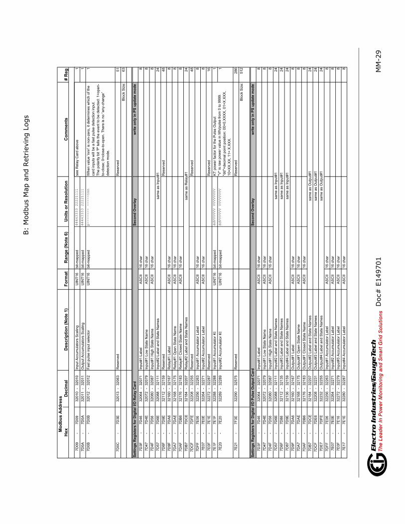
B:
Modbus M
ap a
nd R
etr
ievin
g L
ogs
Doc#
E149701
MM
-29
Electro Industries/GaugeTech
The Leader In Power Monitoring and Smart Grid Solutions
De
sc
rip
tio
n (
No
te 1
)F
orm
at
Ra
ng
e (
No
te 6
)U
nit
s o
r R
es
olu
tio
nC
om
me
nts
# R
eg
Mo
db
us
Ad
dre
ss
Hex
Decim
al
7D
09
-7D
09
32010
-32010
Input
Accum
ula
tors
Scalin
gU
INT
16
bit-m
apped
44443333 22221111
1
7D
0A
-7D
0A
32011
-32011
Outp
ut
Accum
ula
tors
Scalin
gU
INT
16
bit-m
apped
44443333 22221111
1
7D
0B
-7D
0B
32012
-32012
Fast
puls
e input
sele
cto
rU
INT
16
bit-m
apped
p------- -----nnn
When v
alu
e 'nnn' is
non-z
ero
, it d
ete
rmin
es w
hic
h o
f th
e
card
inputs
will
be a
fast
puls
e d
ete
ction input.
The p
ola
rity
bit 'P
' te
lls t
he e
vent
to b
e d
ete
cte
d:
1=
open-
to-c
lose;
0=
clo
se-t
o-o
pen.
There
is n
o “
any-c
hange”
dete
ction m
ode.
1
7D
0C
-7D
3E
32013
-32063
Reserv
ed
Reserv
ed
51
Blo
ck S
ize:
63
Seco
nd
Overl
ay
wri
te o
nly
in
PS
up
date
mo
de
7D
3F
-7D
46
32064
-32071
Input#
1 L
abel
AS
CII
16 c
har
8
7D
47
-7D
4E
32072
-32079
Input#
1 L
ow
Sta
te N
am
eA
SC
II16 c
har
8
7D
4F
-7D
56
32080
-32087
Input#
1 H
igh S
tate
Nam
eA
SC
II16 c
har
8
7D
57
-7D
6E
32088
-32111
Input#
2 L
abel and S
tate
Nam
es
24
7D
6F
-7D
9E
32112
-32159
Reserv
ed
Reserv
ed
48
7D
9F
-7D
A6
32160
-32167
Rela
y#1 L
abel
AS
CII
16 c
har
8
7D
A7
-7D
AE
32168
-32175
Rela
y#1 O
pen S
tate
Nam
eA
SC
II16 c
har
8
7D
AF
-7D
B6
32176
-32183
Rela
y#1 C
losed S
tate
Nam
eA
SC
II16 c
har
8
7D
B7
-7D
CE
32184
-32207
Rela
y#2 L
abel and S
tate
Nam
es
24
7D
CF
-7D
FE
32208
-32255
Reserv
ed
Reserv
ed
48
7D
FF
-7E
06
32256
-32263
Input#
1 A
ccum
ula
tor
Label
AS
CII
16 c
har
8
7E
07
-7E
0E
32264
-32271
Input#
2 A
ccum
ula
tor
Label
AS
CII
16 c
har
8
7E
0F
-7E
1E
32272
-32287
Reserv
ed
Reserv
ed
16
7E
1F
-7E
1F
32288
-32288
Input#
1 A
ccum
ula
tor
Kt
UIN
T16
bit-m
apped
ddVVVVVV VVVVVVVV
1
7E
20
-7E
20
32289
-32289
Input#
2 A
ccum
ula
tor
Kt
UIN
T16
bit-m
apped
ddVVVVVV VVVVVVVV
1
7E
21
-7F
3E
32290
-32575
Reserv
ed
Reserv
ed
286
Blo
ck S
ize:
512
Seco
nd
Overl
ay
wri
te o
nly
in
PS
up
date
mo
de
7D
3F
-7D
46
32064
-32071
Input#
1 L
abel
AS
CII
16 c
har
8
7D
47
-7D
4E
32072
-32079
Input#
1 L
ow
Sta
te N
am
eA
SC
II16 c
har
8
7D
4F
-7D
56
32080
-32087
Input#
1 H
igh S
tate
Nam
eA
SC
II16 c
har
8
7D
57
-7D
6E
32088
-32111
Input#
2 L
abel and S
tate
Nam
es
24
7D
6F
-7D
86
32112
-32135
Input#
3 L
abel and S
tate
Nam
es
24
7D
87
-7D
9E
32136
-32159
Input#
4 L
abel and S
tate
Nam
es
24
7D
9F
-7D
A6
32160
-32167
Outp
ut#
1 L
abel
AS
CII
16 c
har
8
7D
A7
-7D
AE
32168
-32175
Outp
ut#
1 O
pen S
tate
Nam
eA
SC
II16 c
har
8
7D
AF
-7D
B6
32176
-32183
Outp
ut#
1 C
losed S
tate
Nam
eA
SC
II16 c
har
8
7D
B7
-7D
CE
32184
-32207
Outp
ut#
2 L
abel and S
tate
Nam
es
24
7D
CF
-7D
E6
32208
-32231
Outp
ut#
3 L
abel and S
tate
Nam
es
24
7D
E7
-7D
FE
32232
-32255
Outp
ut#
4 L
abel and S
tate
Nam
es
24
7D
FF
-7E
06
32256
-32263
Input#
1 A
ccum
ula
tor
Label
AS
CII
16 c
har
8
7E
07
-7E
0E
32264
-32271
Input#
2 A
ccum
ula
tor
Label
AS
CII
16 c
har
8
7E
0F
-7E
16
32272
-32279
Input#
3 A
ccum
ula
tor
Label
AS
CII
16 c
har
8
7E
17
-7E
1E
32280
-32287
Input#
4 A
ccum
ula
tor
Label
AS
CII
16 c
har
8
see R
ela
y C
ard
above
Sett
ing
s R
eg
iste
rs f
or
Dig
ital
I/O
Rela
y C
ard
sam
e a
s I
nput#
1
sam
e a
s R
ela
y#1
KT
pow
er
facto
r fo
r th
e P
uls
e O
utp
ut
"V"
is r
aw
pow
er
valu
e in W
h/p
uls
e f
rom
0 t
o 9
999.
"dd"=
decim
al poin
t positio
n:
00=
0.X
XX
X,
01=
X.X
XX
,
10=
XX
.XX
, 11=
X.X
XX
.
Sett
ing
s R
eg
iste
rs f
or
Dig
ital
I/O
Pu
lse O
utp
ut
Card
sam
e a
s I
nput#
1
sam
e a
s I
nput#
1
sam
e a
s I
nput#
1
sam
e a
s O
utp
ut#
1
sam
e a
s O
utp
ut#
1
sam
e a
s O
utp
ut#
1

B:
Modbus M
ap a
nd R
etr
ievin
g L
ogs
Doc#
E149701
MM
-30
Electro Industries/GaugeTech
The Leader In Power Monitoring and Smart Grid Solutions
De
sc
rip
tio
n (
No
te 1
)F
orm
at
Ra
ng
e (
No
te 6
)U
nit
s o
r R
es
olu
tio
nC
om
me
nts
# R
eg
Mo
db
us
Ad
dre
ss
Hex
Decim
al
7E
1F
-7E
1F
32288
-32288
Input#
1 A
ccum
ula
tor
Kt
UIN
T16
bit-m
apped
ddVVVVVV VVVVVVVV
1
7E
20
-7E
20
32289
-32289
Input#
2 A
ccum
ula
tor
Kt
UIN
T16
bit-m
apped
ddVVVVVV VVVVVVVV
1
7E
21
-7E
21
32290
-32290
Input#
3 A
ccum
ula
tor
Kt
UIN
T16
bit-m
apped
ddVVVVVV VVVVVVVV
1
7E
22
-7E
22
32291
-32291
Input#
4 A
ccum
ula
tor
Kt
UIN
T16
bit-m
apped
ddVVVVVV VVVVVVVV
1
7E
23
-7F
3E
32292
-32575
Reserv
ed
Reserv
ed
284
Blo
ck S
ize:
512
Seco
nd
Overl
ay
wri
te o
nly
in
PS
up
date
mo
de
7D
3F
-7D
3F
32064
-32064
Update
rate
UIN
T16
0 t
o 6
5535
mill
iseconds
Fix
ed -
- see s
pecific
ations.
1
7D
40
-7D
40
32065
-32065
Channel direction -
1m
A C
ard
only
!U
INT
16
bit-m
apped
-------- ----4321
Full
range o
utp
ut
for
0-1
mA
card
only
: A
bit s
et(
1)
means
full
range (
-1m
A t
o +
1m
A);
a b
it c
leare
d(0
) m
eans s
ourc
e
only
(0m
A t
o +
1m
A).
1
7D
41
-7D
41
32066
-32066
Form
at
para
mete
r fo
r outp
ut
#1
UIN
T16
bit-m
apped
-------- ---f suwb
Form
at
of
the p
olle
d r
egis
ter:
f=float
32;
s=
sig
ned 3
2 b
it
int; u
=unsig
ned 3
2 b
it int; w
=sig
ned 1
6 b
it int;
b=
unsig
ned 1
6 b
it int.
1
7D
42
-7D
42
32067
-32067
Sourc
e r
egis
ter
for
Outp
ut#
1U
INT
16
0 t
o 6
5535
This
regis
ter
should
be p
rogra
mm
ed w
ith t
he a
ddre
ss o
f
the r
egis
ter
whose v
alu
e is t
o b
e u
sed f
or
curr
ent
outp
ut.
In d
iffe
rent
word
s,
the c
urr
ent
level outp
ut
of
analo
g
board
will
follo
w t
he v
alu
e o
f th
e r
egis
ter
addre
ssed h
ere
.
1
7D
43
-7D
44
32068
-32069
Hig
h v
alu
e o
f sourc
e r
egis
ter
for
outp
ut#
1V
alu
e r
ead f
rom
the s
ourc
e r
egis
ter
at
whic
h H
igh
nom
inal curr
ent
will
be o
utp
ut.
Exam
ple
: fo
r th
e 4
-20m
A
card
, if
this
regis
ter
is p
rogra
mm
ed w
ith 7
50,
then t
he
curr
ent
outp
ut
will
be 2
0m
A w
hen t
he v
alu
e r
ead f
rom
the
sourc
e r
egis
ter
is 7
50.
2
7D
45
-7D
46
32070
-32071
Low
valu
e o
f sourc
e r
egis
ter
for
outp
ut#
1V
alu
e r
ead f
rom
the s
ourc
e r
egis
ter
at
whic
h L
ow
nom
inal curr
ent
will
be o
utp
ut.
Exam
ple
: fo
r th
e 4
-20m
A
card
, if
this
regis
ter
is p
rogra
mm
ed w
ith 0
, th
en t
he
curr
ent
outp
ut
will
be 4
mA
when t
he v
alu
e r
ead f
rom
the
sourc
e r
egis
ter
is 0
.
2
7D
47
-7D
4C
32072
-32077
Analo
g o
utp
ut#
2 f
orm
at, r
egis
ter,
max &
min
6
7D
4D
-7D
52
32078
-32083
Analo
g o
utp
ut#
3 f
orm
at, r
egis
ter,
max &
min
6
7D
53
-7D
58
32084
-32089
Analo
g o
utp
ut#
4 f
orm
at, r
egis
ter,
max &
min
6
7D
59
-7F
3E
32090
-32575
Reserv
ed
Reserv
ed
486
Blo
ck S
ize:
512
KT
pow
er
facto
r fo
r th
e a
ccum
ula
tor
input
"V"
is r
aw
pow
er
valu
e in W
h/p
uls
e f
rom
0 t
o 9
999.
"dd"=
decim
al poin
t positio
n:
00=
0.X
XX
X,
01=
X.X
XX
,
10=
XX
.XX
, 11=
X.X
XX
.
Sett
ing
s R
eg
iste
rs f
or
An
alo
g O
ut
0-1
mA
/ A
nalo
g O
ut
4-2
0m
A C
ard
s
Depends o
n t
he f
orm
at
para
mete
r
Depends o
n t
he f
orm
at
para
mete
r Sam
e a
s a
nalo
g o
utp
ut#
1
Sam
e a
s a
nalo
g o
utp
ut#
1
Sam
e a
s a
nalo
g o
utp
ut#
1

B:
Modbus M
ap a
nd R
etr
ievin
g L
ogs
Doc#
E149701
MM
-31
Electro Industries/GaugeTech
The Leader In Power Monitoring and Smart Grid Solutions
De
sc
rip
tio
n (
No
te 1
)F
orm
at
Ra
ng
e (
No
te 6
)U
nit
s o
r R
es
olu
tio
nC
om
me
nts
# R
eg
Mo
db
us
Ad
dre
ss
He
xD
ec
ima
l
Seco
nd
Overl
ay
wri
te o
nly
in
PS
up
date
mo
de
7D
3F
-7D
3F
32064
-32064
Genera
l O
ptions
bit-m
apped
----
-DG
T -
---
-W--
W=
Web s
erv
er:
0=
Enable
d, 1=
Dis
able
d
T=
Sile
ntm
ode:0
=D
isable
d, 1=
Enable
d
(W
hen e
nable
d T
CP
/Reset is
not sent w
hen
C
onnection is a
ttem
pte
d to a
n u
nbound p
ort
)
G=
Modbus T
cp/Ip G
ate
way:0
=E
nable
d,1
=D
isable
d
D=
DN
P-T
cp/Ip-W
rapper:
0=
Dis
able
d, 1=
Enable
d.
1
7D
40
-7D
40
32065
-32065
DH
CP
enable
bit-m
apped
-------- -------d
DH
CP
: d=
1 e
nable
d, d=
0 d
isable
d (
user
must pro
vid
e IP
configura
tion).
1
7D
41
-7D
48
32066
-32073
Host nam
e label
AS
CII
16 b
yte
s (
8 r
egis
ters
)8
7D
49
-7D
4C
32074
-32077
IP c
ard
netw
ork
addre
ss
UIN
T16
0 to 2
55 (
IPv4)
These 4
regis
ters
hold
the 4
num
bers
(1 n
um
ber
each
regis
ter)
that m
ake the IP
addre
ss u
sed b
y the c
ard
.
4
7D
4D
-7D
4D
32078
-32078
IP n
etw
ork
addre
ss m
ask length
UIN
T16
0 to 3
2N
um
ber
of bits that are
set in
the IP
addre
ss m
ask,
sta
rtin
g fro
m the M
sb o
f th
e 3
2 b
it w
ord
.
Exam
ple
24 =
255.2
55.2
55.0
; a v
alu
e o
f 2 w
ould
mean
192.0
.0.0
1
7D
4E
-7D
51
32079
-32082
IP c
ard
netw
ork
gate
way a
ddre
ss
UIN
T16
0 to 2
55 (
IPv4)
These 4
regis
ters
hold
the 4
num
bers
that m
ake the IP
gate
way a
ddre
ss o
n n
etw
ork
.
4
7D
52
-7D
55
32083
-32086
DN
S #
1, IP
addre
ss
UIN
T16
0 to 2
55 (
IPv4)
IP a
ddre
ss o
f th
e D
NS
#1 o
n the n
etw
ork
.4
7D
56
-7D
59
32087
-32090
DN
S #
2, IP
addre
ss
UIN
T16
0 to 2
55 (
IPv4)
IP a
ddre
ss o
f th
e D
NS
#2 o
n the n
etw
ork
.4
7D
5A
-7D
5A
32091
-32091
TC
P/IP
Port
– M
odbus G
ate
way S
erv
ice
UIN
T16
32-6
5534
Port
for
the G
ate
way s
erv
ice (
modbus tcp/ip)
when
enable
d
1
7D
5B
-7D
5B
32092
-32092
TC
P/IP
Port
– W
ebS
erv
ice
UIN
T16
32-6
5534
Port
for
the W
eb s
erv
ice (
htm
l vie
wer)
when e
nable
d1
7D
5C
-7D
5C
32093
-32093
Reserv
ed –
must be s
et to
0R
eserv
ed. S
et th
ese r
egs to z
ero
.1
7D
5D
-7D
5D
32094
-32094
Reserv
ed –
must be s
et to
0R
eserv
ed. S
et th
ese r
egs to z
ero
.1
7D
5E
-7D
61
32095
-32098
Reserv
ed –
must be s
et to
0R
eserv
ed. S
et th
ese r
egs to z
ero
.4
7D
62
-7D
65
32099
-32102
Reserv
ed –
must be s
et to
0R
eserv
ed. S
et th
ese r
egs to z
ero
.4
7D
66
-7D
66
32103
-32103
Reserv
ed –
must be s
et to
0R
eserv
ed. S
et th
ese r
egs to z
ero
.1
7D
67
-7D
67
32104
-32104
Reserv
ed –
must be s
et to
0R
eserv
ed. S
et th
ese r
egs to z
ero
.1
7D
68
-7D
6C
32105
-32109
Reserv
ed –
must be s
et to
0R
eserv
ed. S
et th
ese r
egs to z
ero
.5
7D
6D
-7D
8C
32110
-32141
NT
P1 U
RL o
r IP
(str
ing)
IP a
ddre
ss o
f th
e N
TP
serv
er
the S
hark
will
conta
ct.
32
7D
8D
-7D
AC
32142
-32173
Reserv
ed –
must be s
et to
0S
et th
ese to r
egs to z
ero
. S
hark
uses o
nly
1 N
TP
32
7D
AD
-7F
3E
32174
-32575
Reserv
ed –
must be s
et to
0R
eserv
ed. S
et th
ese r
egs to z
ero
.402
Blo
ck S
ize:
512
wri
te o
nly
in
PS
up
date
mo
de
80E
7 -
80E
733000
-33000
Cla
ss ID
of th
e O
ption C
ard
2 S
ettin
gs
UIN
T16
bit-m
apped
----
----
cccctttt
Whic
h c
lass (
cccc)
and type(t
ttt)
of card
the O
ption
Settin
gs for
Card
2 a
pply
to. S
ee n
ote
22
1
80E
8-
8126
33001
-33063
Settin
gs for
Option C
ard
2, F
irst O
verlay -
- see
belo
w
63
8127
-8326
33064
-33575
Settin
gs for
Option C
ard
2, S
econd O
verlay -
-
see b
elo
w
512
Blo
ck S
ize:
576
Pro
gra
mm
ab
le S
ett
ing
s f
or
Op
tio
n C
ard
2O
pti
on
Card
2 S
etu
ps B
lock
Regis
ter
assig
nm
ents
depend o
n w
hic
h type o
f card
is in the s
lot. S
ee o
verlays b
elo
w.
Regis
ter
assig
nm
ents
depend o
n w
hic
h type o
f card
is in the s
lot. S
ee o
verlays b
elo
w.
Sett
ing
s R
eg
iste
rs f
or
Netw
ork
Card
s

B:
Modbus M
ap a
nd R
etr
ievin
g L
ogs
Doc#
E149701
MM
-32
Electro Industries/GaugeTech
The Leader In Power Monitoring and Smart Grid Solutions
De
sc
rip
tio
n (
No
te 1
)F
orm
at
Ra
ng
e (
No
te 6
)U
nit
s o
r R
es
olu
tio
nC
om
me
nts
# R
eg
Mo
db
us
Ad
dre
ss
Hex
Decim
al
Fir
st
Overl
ay
wri
te o
nly
in
PS
up
date
mo
de
80E
8-
80E
833001
-33001
Sla
ve a
ddre
ss
UIN
T16
1~
247 (
for
Modbus)
1~
65534 (
for
DN
P)
none
Sla
ve a
ddre
ss o
f th
e u
nit.
The c
om
munic
ation c
apable
card
is a
lways a
maste
r.
Set
to 0
when a
n a
nalo
g b
oard
is insta
lled.
1
80E
9-
80E
933002
-33002
Speed a
nd f
orm
at
UIN
T16
bit-m
apped
-abcde-- fghijklm
Bps:
a=
57600;
b=
38400;
c=
19200;
d=
14400;
e=
9600
Sto
p b
its 'f':
cle
are
d 1
sto
p b
it,
set
2 s
top b
its
Parity
: g=
even;
h=
odd;
i=none
Data
bits:
j=8;
k=
7;
l=6;
m=
5
Set
to 0
when a
n a
nalo
g b
oard
is insta
lled.
1
80E
A-
80E
A33003
-33003
Reserv
ed
UIN
T16
bit-m
apped
Reserv
ed
1
80E
B-
80E
B33004
-33004
Pro
tocol
UIN
T16
bit-m
apped
-------- -----ppp-
ppp=
100 =
DN
P3;
010=
Ascii
Modbus;
001=
Rtu
Modbus
Set
to 0
when a
n a
nalo
g b
oard
is insta
lled.
1
80E
C-
80E
C33005
-33005
Reply
dela
yU
INT
16
0 t
o 6
5535
mill
iseconds
Dela
y t
o r
eply
to a
Modbus t
ransaction a
fter
receiv
ing it.
Set
to 0
when a
n a
nalo
g b
oard
is insta
lled
1
80E
D-
8126
33006
-33063
Reserv
ed
Reserv
ed
58
Blo
ck S
ize:
63
Fir
st
Overl
ay
wri
te o
nly
in
PS
up
date
mo
de
80E
8-
80E
833001
-33001
Input#
1 -
2
bin
din
gs &
loggin
g e
nable
sU
INT
16
bit-m
apped
-------- 2222 1111
One n
ibble
for
each input.
Assum
ing
"abcc"
as t
he b
its in e
ach n
ibble
:
"a":
sele
ct
this
input
for
EO
I (E
nd O
f In
terv
al)puls
e
sensin
g.
"b":
log t
his
input
when p
uls
e is d
ete
cte
d
"cc":
Input
event
trig
ger
mode -
Conta
ct
sensin
g m
eth
od;
00 =
none;
01 =
open t
o c
lose;
10 =
clo
se t
o o
pen;
11 =
any c
hange.
Every
input
has a
n a
ssocia
ted inte
rnal accum
ula
tor
(See
input
Accum
ula
tor
Scalin
g),
whic
h is incre
mente
d e
very
tim
e t
he input
changes a
ccord
ing w
ith t
he t
rigger
mode
criete
ria “
cc”
1
80E
9-
80E
933002
-33002
Rela
y #
1 D
ela
y t
o O
pera
teU
INT
16
0.1
second u
nits
Dela
y t
o o
pera
te t
he r
ela
y s
ince r
equest.
1
80E
A-
80E
A33003
-33003
Rela
y #
1 D
ela
y t
o R
ele
ase
UIN
T16
0.1
second u
nits
Dela
y t
o r
ele
ase t
he r
ela
y s
ince r
equest.
1
80E
B-
80F
033004
-33009
Reserv
ed
UIN
T16
Set
to 0
.6
80F
1-
80F
133010
-33010
Rela
y #
2 D
ela
y t
o O
pera
teU
INT
16
0.1
second u
nits
Dela
y t
o o
pera
te t
he r
ela
y s
ince r
equest.
1
80F
2-
80F
233011
-33011
Rela
y #
2 D
ela
y t
o R
ele
ase
UIN
T16
0.1
second u
nits
Dela
y t
o r
ele
ase t
he r
ela
y s
ince r
equest.
1
80F
3-
8108
33012
-33033
Reserv
ed
UIN
T16
Set
to 0
.22
8109
-8109
33034
-33034
Input
Accum
ula
tors
Scalin
gU
INT
16
bit-m
apped
-------- 22221111
1
810A
-810A
33035
-33035
Rela
y A
ccum
ula
tors
Scalin
gU
INT
16
bit-m
apped
-------- 22221111
1
Ov
erl
ay
s f
or
Op
tio
n C
ard
2 P
rog
ram
ma
ble
Se
ttin
gs
Sett
ing
s R
eg
iste
rs f
or
an
y c
om
mu
nic
ati
on
cap
ab
le c
ard
, in
clu
din
g n
etw
ork
an
d a
nalo
g c
ard
s
Sett
ing
s R
eg
iste
rs f
or
Dig
ital
I/O
Rela
y C
ard
4 b
its p
er
input
or
outp
ut
accum
ula
tor
The n
ibble
info
rms w
hat
should
be t
he s
calin
g o
f th
e
accum
ula
tor
0=
no-s
calin
g,
1=
0.1
, 2=
0.0
1,
3=
1m
,
4=
0.1
m,
5=
0.0
1m
, 6=
1u,
7=
0.1
u;
the v
alu
e 1
5 d
isable
the a
ccum
ula
tor.
Exam
ple
: suppose t
hat
the inte
rnal in
put
accum
ula
tor
#1
is 1
2345,
and its
corr
espondin
g s
calin
g s
ettin
g is “
0011”
(3 d
ecim
al).
Then,
the a
ccum
ula
tor
will
be r
ead a
s:
Scalin
g 3
, m
eans 1
m o
r 0.0
01.
Scale
d a
ccum
ula
tor
= 1
2345 *
0.0
01 =
12 (
Tw
elv
e).
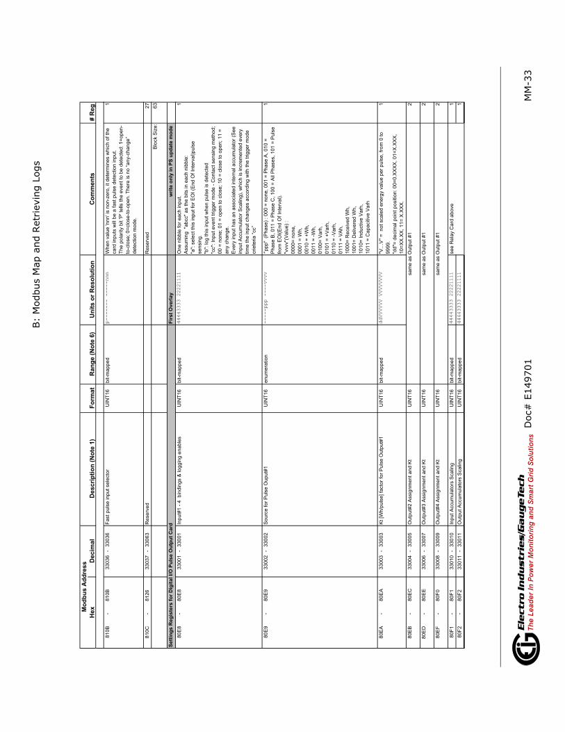
B:
Modbus M
ap a
nd R
etr
ievin
g L
ogs
Doc#
E149701
MM
-33
Electro Industries/GaugeTech
The Leader In Power Monitoring and Smart Grid Solutions
De
sc
rip
tio
n (
No
te 1
)F
orm
at
Ra
ng
e (
No
te 6
)U
nit
s o
r R
es
olu
tio
nC
om
me
nts
# R
eg
Mo
db
us
Ad
dre
ss
Hex
Decim
al
810B
-810B
33036
-33036
Fast
puls
e input
sele
cto
rU
INT
16
bit-m
apped
p------- -----nnn
When v
alu
e 'nnn' is
non-z
ero
, it d
ete
rmin
es w
hic
h o
f th
e
card
inputs
will
be a
fast
puls
e d
ete
ction input.
The p
ola
rity
bit 'P
' te
lls t
he e
vent
to b
e d
ete
cte
d:
1=
open-
to-c
lose;
0=
clo
se-t
o-o
pen.
There
is n
o “
any-c
hange”
dete
ction m
ode.
1
810C
-8126
33037
-33063
Reserv
ed
Reserv
ed
27
Blo
ck S
ize:
63
Fir
st
Overl
ay
wri
te o
nly
in
PS
up
date
mo
de
80E
8-
80E
833001
-33001
Input#
1 -
4
bin
din
gs &
loggin
g e
nable
sU
INT
16
bit-m
apped
44443333 22221111
One n
ibble
for
each input.
Assum
ing
"abcc"
as t
he b
its in e
ach n
ibble
:
"a":
sele
ct
this
input
for
EO
I (E
nd O
f In
terv
al)puls
e
sensin
g.
"b":
log t
his
input
when p
uls
e is d
ete
cte
d
"cc":
Input
event
trig
ger
mode -
Conta
ct
sensin
g m
eth
od;
00 =
none;
01 =
open t
o c
lose;
10 =
clo
se t
o o
pen;
11 =
any c
hange.
Every
input
has a
n a
ssocia
ted inte
rnal accum
ula
tor
(See
input
Accum
ula
tor
Scalin
g),
whic
h is incre
mente
d e
very
tim
e t
he input
changes a
ccord
ing w
ith t
he t
rigger
mode
criete
ria “
cc”
1
80E
9-
80E
933002
-33002
Sourc
e f
or
Puls
e O
uput#
1U
INT
16
enum
era
tion
-----ppp ----vvvv
"ppp"
(Phase)
: 000 =
none,
001 =
Phase A
, 010 =
Phase B
, 011 =
Phase C
, 100 =
All
Phases,
101 =
Puls
e
from
EO
I(E
nd O
f In
terv
al).
"vvvv"(
Valu
e)
:
0000=
none,
0001 =
Wh,
0010 =
+W
h,
0011 =
-W
h,
0100=
Varh
,
0101 =
+V
arh
,
0110 =
-V
arh
,
0111 =
VA
h,
1000=
Receiv
ed W
h,
1001=
Deliv
ere
d W
h,
1010=
Inductive V
arh
,
1011 =
Capacitiv
e V
arh
1
80E
A-
80E
A33003
-33003
Kt
[Wh/p
uls
e]
facto
r fo
r P
uls
e O
utp
ut#
1U
INT
16
bit-m
apped
ddVVVVVV VVVVVVVV
"V…
V"
=
not
scale
d e
nerg
y v
alu
e p
er
puls
e,
from
0 t
o
9999.
"dd"=
decim
al poin
t positio
n:
00=
0.X
XX
X,
01=
X.X
XX
,
10=
XX
.XX
, 11=
X.X
XX
.
1
80E
B-
80E
C33004
-33005
Outp
ut#
2 A
ssig
nm
ent
and K
tU
INT
16
2
80E
D-
80E
E33006
-33007
Outp
ut#
3 A
ssig
nm
ent and K
tU
INT
16
2
80E
F-
80F
033008
-33009
Outp
ut#
4 A
ssig
nm
ent
and K
tU
INT
16
2
80F
1-
80F
133010
-33010
Input
Accum
ula
tors
Scalin
gU
INT
16
bit-m
apped
44443333 22221111
1
80F
2-
80F
233011
-33011
Outp
ut
Accum
ula
tors
Scalin
gU
INT
16
bit-m
apped
44443333 22221111
1
Sett
ing
s R
eg
iste
rs f
or
Dig
ital
I/O
Pu
lse O
utp
ut
Card
sam
e a
s O
utp
ut
#1
sam
e a
s O
utp
ut
#1
sam
e a
s O
utp
ut
#1
see R
ela
y C
ard
above

B:
Modbus M
ap a
nd R
etr
ievin
g L
ogs
Doc#
E149701
MM
-34
Electro Industries/GaugeTech
The Leader In Power Monitoring and Smart Grid Solutions
De
sc
rip
tio
n (
No
te 1
)F
orm
at
Ra
ng
e (
No
te 6
)U
nit
s o
r R
es
olu
tio
nC
om
me
nts
# R
eg
Mo
db
us
Ad
dre
ss
Hex
Decim
al
80F
3-
80F
333012
-33012
Fast
puls
e input
sele
cto
rU
INT
16
bit-m
apped
p------- -----nnn
When v
alu
e 'nnn' is
non-z
ero
, it d
ete
rmin
es w
hic
h o
f th
e
card
inputs
will
be a
fast
puls
e d
ete
ction input.
The p
ola
rity
bit 'P
' te
lls t
he e
vent
to b
e d
ete
cte
d:
1=
open-
to-c
lose;
0=
clo
se-t
o-o
pen.
There
is n
o “
any-c
hange”
dete
ction m
ode.
1
80F
4-
8126
33013
-33063
Reserv
ed
Reserv
ed
51
Blo
ck S
ize:
63
Seco
nd
Overl
ay
wri
te o
nly
in
PS
up
date
mo
de
8127
-812E
33064
-33071
Input#
1 L
abel
AS
CII
16 c
har
8
812F
-8136
33072
-33079
Input#
1 L
ow
Sta
te N
am
eA
SC
II16 c
har
8
8137
-813E
33080
-33087
Input#
1 H
igh S
tate
Nam
eA
SC
II16 c
har
8
813F
-8156
33088
-33111
Input#
2 L
abel and S
tate
Nam
es
24
8157
-8186
33112
-33159
Reserv
ed
48
8187
-818E
33160
-33167
Rela
y#1 L
abel
AS
CII
16 c
har
8
818F
-8196
33168
-33175
Rela
y#1 O
pen S
tate
Nam
eA
SC
II16 c
har
8
8197
-819E
33176
-33183
Rela
y#1 C
losed S
tate
Nam
eA
SC
II16 c
har
8
819F
-81B
633184
-33207
Rela
y#2 L
abel and S
tate
Nam
es
24
81B
7-
81E
633208
-33255
Reserv
ed
48
81E
7-
81E
E33256
-33263
Input#
1 A
ccum
ula
tor
Label
AS
CII
16 c
har
8
81E
F-
81F
633264
-33271
Input#
2 A
ccum
ula
tor
Label
AS
CII
16 c
har
8
8208
-8208
33289
-33289
Input#
2 A
ccum
ula
tor
Kt
UIN
T16
bit-m
apped
ddVVVVVV VVVVVVVV
1
8209
-8326
33290
-33575
Reserv
ed
286
Blo
ck S
ize:
512
Se
co
nd
Ov
erl
ay
wri
te o
nly
in
PS
up
da
te m
od
e
8127
-812E
33064
-33071
Input#
1 L
abel
AS
CII
16 c
har
8
812F
-8136
33072
-33079
Input#
1 L
ow
Sta
te N
am
eA
SC
II16 c
har
8
8137
-813E
33080
-33087
Input#
1 H
igh S
tate
Nam
eA
SC
II16 c
har
8
813F
-8156
33088
-33111
Input#
2 L
abel and S
tate
Nam
es
24
8157
-816E
33112
-33135
Input#
3 L
abel and S
tate
Nam
es
24
816F
-8186
33136
-33159
Input#
4 L
abel and S
tate
Nam
es
24
8187
-818E
33160
-33167
Outp
ut#
1 L
abel
AS
CII
16 c
har
8
818F
-8196
33168
-33175
Outp
ut#
1 O
pen S
tate
Nam
eA
SC
II16 c
har
8
8197
-819E
33176
-33183
Outp
ut#
1 C
losed S
tate
Nam
eA
SC
II16 c
har
8
819F
-81B
633184
-33207
Outp
ut#
2 L
abel and S
tate
Nam
es
24
81B
7-
81C
E33208
-33231
Outp
ut#
3 L
abel and S
tate
Nam
es
24
81C
F-
81E
633232
-33255
Outp
ut#
4 L
abel and S
tate
Nam
es
24
81E
7-
81E
E33256
-33263
Input#
1 A
ccum
ula
tor
Label
AS
CII
16 c
har
8
81E
F-
81F
633264
-33271
Input#
2 A
ccum
ula
tor
Label
AS
CII
16 c
har
8
81F
7-
81F
E33272
-33279
Input#
3 A
ccum
ula
tor
Label
AS
CII
16 c
har
8
Sett
ing
s R
eg
iste
rs f
or
Dig
ital
I/O
Rela
y C
ard
sam
e a
s I
nput#
1
sam
e a
s R
ela
y#1
KT
pow
er
facto
r fo
r th
e P
uls
e O
utp
ut
"V"
is r
aw
pow
er
valu
e in W
h/p
uls
e f
rom
0 t
o 9
999.
"dd"=
decim
al poin
t positio
n:
00=
0.X
XX
X,
01=
X.X
XX
,
10=
XX
.XX
, 11=
X.X
XX
.
Sett
ing
s R
eg
iste
rs f
or
Dig
ital
I/O
Pu
lse O
utp
ut
Card
sam
e a
s I
nput#
1
sam
e a
s I
nput#
1
sam
e a
s I
nput#
1
sam
e a
s O
utp
ut#
1
sam
e a
s O
utp
ut#
1
sam
e a
s O
utp
ut#
1

B:
Modbus M
ap a
nd R
etr
ievin
g L
ogs
Doc#
E149701
MM
-35
Electro Industries/GaugeTech
The Leader In Power Monitoring and Smart Grid Solutions
De
sc
rip
tio
n (
No
te 1
)F
orm
at
Ra
ng
e (
No
te 6
)U
nit
s o
r R
es
olu
tio
nC
om
me
nts
# R
eg
Mo
db
us
Ad
dre
ss
Hex
Decim
al
81F
F-
8206
33280
-33287
Input#
4 A
ccum
ula
tor
Label
AS
CII
16 c
har
8
8207
-8207
33288
-33288
Input#
1 A
ccum
ula
tor
Kt
UIN
T16
bit-m
apped
ddVVVVVV VVVVVVVV
1
8208
-8208
33289
-33289
Input#
2 A
ccum
ula
tor
Kt
UIN
T16
bit-m
apped
ddVVVVVV VVVVVVVV
1
8209
-8209
33290
-33290
Input#
3 A
ccum
ula
tor
Kt
UIN
T16
bit-m
apped
ddVVVVVV VVVVVVVV
1
820A
-820A
33291
-33291
Input#
4 A
ccum
ula
tor
Kt
UIN
T16
bit-m
apped
ddVVVVVV VVVVVVVV
1
820B
-8326
33292
-33575
Reserv
ed
Reserv
ed
284
Blo
ck S
ize:
512
Seco
nd
Overl
ay
wri
te o
nly
in
PS
up
date
mo
de
8127
-8127
33064
-33064
Update
rate
UIN
T16
0 t
o 6
5535
mill
iseconds
Fix
ed -
- see s
pecific
ations.
1
8128
-8128
33065
-33065
Channel direction -
1m
A C
ard
only
!U
INT
16
bit-m
apped
-------- ----4321
Full
range o
utp
ut
for
0-1
mA
card
only
: A
bit s
et(
1)
means
full
range (
-1m
A t
o +
1m
A);
a b
it c
leare
d(0
) m
eans s
ourc
e
only
(0m
A t
o +
1m
A).
1
8129
-8129
33066
-33066
Form
at
para
mete
r fo
r outp
ut
#1
UIN
T16
bit-m
apped
-------- ---f suwb
Form
at
of
the p
olle
d r
egis
ter:
f=float
32;
s=
sig
ned 3
2 b
it
int; u
=unsig
ned 3
2 b
it int; w
=sig
ned 1
6 b
it int;
b=
unsig
ned 1
6 b
it int.
1
812A
-812A
33067
-33067
Sourc
e r
egis
ter
for
Outp
ut#
1U
INT
16
0 t
o 6
5535
This
regis
ter
should
be p
rogra
mm
ed w
ith t
he a
ddre
ss o
f
the r
egis
ter
whose v
alu
e is t
o b
e u
sed f
or
curr
ent
outp
ut.
In d
iffe
rent
word
s,
the c
urr
ent
level outp
ut
of
analo
g
board
will
follo
w t
he v
alu
e o
f th
e r
egis
ter
addre
ssed h
ere
.
1
812B
-812C
33068
-33069
Hig
h v
alu
e o
f sourc
e r
egis
ter
for
outp
ut#
1V
alu
e r
ead f
rom
the s
ourc
e r
egis
ter
at
whic
h H
igh
nom
inal curr
ent
will
be o
utp
ut.
Exam
ple
: fo
r th
e 4
-20m
A
card
, if
this
regis
ter
is p
rogra
mm
ed w
ith 7
50,
then t
he
curr
ent
outp
ut
will
be 2
0m
A w
hen t
he v
alu
e r
ead f
rom
the
sourc
e r
egis
ter
is 7
50.
2
812D
-812E
33070
-33071
Low
valu
e o
f sourc
e r
egis
ter
for
outp
ut#
1V
alu
e r
ead f
rom
the s
ourc
e r
egis
ter
at
whic
h L
ow
nom
inal curr
ent
will
be o
utp
ut.
Exam
ple
: fo
r th
e 4
-20m
A
card
, if
this
regis
ter
is p
rogra
mm
ed w
ith 0
, th
en t
he
curr
ent
outp
ut
will
be 4
mA
when t
he v
alu
e r
ead f
rom
the
sourc
e r
egis
ter
is 0
.
2
812F
-8134
33072
-33077
Analo
g o
utp
ut#
2 f
orm
at, r
egis
ter,
max &
min
6
8135
-813A
33078
-33083
Analo
g o
utp
ut#
3 f
orm
at, r
egis
ter,
max &
min
6
813B
-8140
33084
-33089
Analo
g o
utp
ut#
4 f
orm
at, r
egis
ter,
max &
min
6
8141
-8326
33090
-33575
Reserv
ed
Reserv
ed
486
Blo
ck S
ize:
512
KT
pow
er
facto
r fo
r th
e a
ccum
ula
tor
input
"V"
is r
aw
pow
er
valu
e in W
h/p
uls
e f
rom
0 t
o 9
999.
"dd"=
decim
al poin
t positio
n:
00=
0.X
XX
X,
01=
X.X
XX
,
10=
XX
.XX
, 11=
X.X
XX
.
Sett
ing
s R
eg
iste
rs f
or
An
alo
g O
ut
0-1
mA
/ A
nalo
g O
ut
4-2
0m
A C
ard
s
Depends o
n t
he f
orm
at
para
mete
r
Depends o
n t
he f
orm
at
para
mete
r Sam
e a
s a
nalo
g o
utp
ut#
1
Sam
e a
s a
nalo
g o
utp
ut#
1
Sam
e a
s a
nalo
g o
utp
ut#
1

B:
Modbus M
ap a
nd R
etr
ievin
g L
ogs
Doc#
E149701
MM
-36
Electro Industries/GaugeTech
The Leader In Power Monitoring and Smart Grid Solutions
De
sc
rip
tio
n (
No
te 1
)F
orm
at
Ra
ng
e (
No
te 6
)U
nit
s o
r R
es
olu
tio
nC
om
me
nts
# R
eg
Mo
db
us
Ad
dre
ss
He
xD
ec
ima
l
Seco
nd
Overl
ay
wri
te o
nly
in
PS
up
date
mo
de
8127
-8127
33064
-33064
Genera
l O
ptions
bit-m
apped
----
-DG
T -
---
-W--
W=
Web s
erv
er:
0=
Enable
d, 1=
Dis
able
d
T=
Sile
ntm
ode:0
=D
isable
d, 1=
Enable
d
(W
hen e
nable
d T
CP
/Reset is
not sent w
hen
C
onnection is a
ttem
pte
d to a
n u
nbound p
ort
)
G=
Modbus T
cp/Ip G
ate
way:0
=E
nable
d,1
=D
isable
d
D=
DN
P-T
cp/Ip-W
rapper:
0=
Dis
able
d, 1=
Enable
d.
1
8128
-8128
33065
-33065
DH
CP
enable
bit-m
apped
-------- -------d
DH
CP
: d=
1 e
nable
d, d=
0 d
isable
d (
user
must pro
vid
e IP
configura
tion).
1
8129
-8130
33066
-33073
Host nam
e label
AS
CII
16 b
yte
s (
8 r
egis
ters
)8
8131
-8134
33074
-33077
IP c
ard
netw
ork
addre
ss
UIN
T16
0 to 2
55 (
IPv4)
These 4
regis
ters
hold
the 4
num
bers
(1 n
um
ber
each
regis
ter)
that m
ake the IP
addre
ss u
sed b
y the c
ard
.
4
8135
-8135
33078
-33078
IP n
etw
ork
addre
ss m
ask length
UIN
T16
0 to 3
2N
um
ber
of bits that are
set in
the IP
addre
ss m
ask,
sta
rtin
g fro
m the M
sb o
f th
e 3
2 b
it w
ord
.
Exam
ple
24 =
255.2
55.2
55.0
; a v
alu
e o
f 2 w
ould
mean
192.0
.0.0
1
8136
-8139
33079
-33082
IP c
ard
netw
ork
gate
way a
ddre
ss
UIN
T16
0 to 2
55 (
IPv4)
These 4
regis
ters
hold
the 4
num
bers
that m
ake the IP
gate
way a
ddre
ss o
n n
etw
ork
.
4
813A
-813D
33083
-33086
DN
S #
1, IP
addre
ss
UIN
T16
0 to 2
55 (
IPv4)
IP a
ddre
ss o
f th
e D
NS
#1 o
n the n
etw
ork
.4
813E
-8141
33087
-33090
DN
S #
2, IP
addre
ss
UIN
T16
0 to 2
55 (
IPv4)
IP a
ddre
ss o
f th
e D
NS
#2 o
n the n
etw
ork
.4
8142
-8142
33091
-33091
TC
P/IP
Port
– M
odbus G
ate
way S
erv
ice
UIN
T16
32-6
5534
Port
for
the G
ate
way s
erv
ice (
modbus tcp/ip)
when
enable
d
1
8143
-8143
33092
-33092
TC
P/IP
Port
– W
ebS
erv
ice
UIN
T16
32-6
5534
Port
for
the W
eb s
erv
ice (
htm
l vie
wer)
when e
nable
d1
8144
-8144
33093
-33093
Reserv
ed –
must be s
et to
0R
eserv
ed. S
et th
ese r
egs to z
ero
.1
8145
-8145
33094
-33094
Reserv
ed –
must be s
et to
0R
eserv
ed. S
et th
ese r
egs to z
ero
.1
8146
-8149
33095
-33098
Reserv
ed –
must be s
et to
0R
eserv
ed. S
et th
ese r
egs to z
ero
.4
814A
-814D
33099
-33102
Reserv
ed –
must be s
et to
0R
eserv
ed. S
et th
ese r
egs to z
ero
.4
814E
-814E
33103
-33103
Reserv
ed –
must be s
et to
0R
eserv
ed. S
et th
ese r
egs to z
ero
.1
814F
-814F
33104
-33104
Reserv
ed –
must be s
et to
0R
eserv
ed. S
et th
ese r
egs to z
ero
.1
8150
-8154
33105
-33109
Reserv
ed –
must be s
et to
0R
eserv
ed. S
et th
ese r
egs to z
ero
.5
8155
-8174
33110
-33141
NT
P1 U
RL o
r IP
(str
ing)
IP a
ddre
ss o
f th
e N
TP
serv
er
the S
hark
will
conta
ct.
32
8175
-8194
33142
-33173
Reserv
ed –
must be s
et to
0S
et th
ese to r
egs to z
ero
. S
hark
uses o
nly
1 N
TP
32
8195
-8326
33174
-33575
Reserv
ed –
must be s
et to
0R
eserv
ed. S
et th
ese r
egs to z
ero
.402
Blo
ck S
ize:
512
read
-on
ly e
xcep
t as n
ote
d
9C
40
-9C
40
40001
-40001
Syste
m S
anity Indic
ato
rU
INT
16
0 o
r 1
none
0 indic
ate
s p
roper
mete
r opera
tion
1
9C
41
-9C
41
40002
-40002
Volts A
-NU
INT
16
2047 to 4
095
volts
2047=
0, 4095=
+150
1
9C
42
-9C
42
40003
-40003
Volts B
-NU
INT
16
2047 to 4
095
volts
1
9C
43
-9C
43
40004
-40004
Volts C
-NU
INT
16
2047 to 4
095
volts
1
9C
44
-9C
44
40005
-40005
Am
ps A
UIN
T16
0 to 4
095
am
ps
0=
-10, 2047=
0, 4095=
+10
1
9C
45
-9C
45
40006
-40006
Am
ps B
UIN
T16
0 to 4
095
am
ps
1
9C
46
-9C
46
40007
-40007
Am
ps C
UIN
T16
0 to 4
095
am
ps
1
9C
47
-9C
47
40008
-40008
Watts, 3-P
h tota
lU
INT
16
0 to 4
095
watts
0=
-3000, 2047=
0, 4095=
+3000
1
9C
48
-9C
48
40009
-40009
VA
Rs, 3-P
h tota
lU
INT
16
0 to 4
095
VA
Rs
watts, V
AR
s, V
As =
1
9C
49
-9C
49
40010
-40010
VA
s, 3-P
h tota
lU
INT
16
2047 to 4
095
VA
s3000 *
(re
gis
ter
- 2047)
/ 2047
1
Se
co
nd
ary
Re
ad
ing
sS
ec
tio
nS
eco
nd
ary
Blo
ck
volts =
150 *
(re
gis
ter
- 2047)
/ 2047
am
ps =
10 *
(re
gis
ter
- 2047)
/ 2047
Sett
ing
s R
eg
iste
rs f
or
Netw
ork
Card
s

B:
Modbus M
ap a
nd R
etr
ievin
g L
ogs
Doc#
E149701
MM
-37
Electro Industries/GaugeTech
The Leader In Power Monitoring and Smart Grid Solutions
De
sc
rip
tio
n (
No
te 1
)F
orm
at
Ra
ng
e (
No
te 6
)U
nit
s o
r R
es
olu
tio
nC
om
me
nts
# R
eg
Mo
db
us
Ad
dre
ss
Hex
Decim
al
9C
4A
-9C
4A
40011
-40011
Pow
er
Facto
r, 3
-Ph t
ota
lU
INT
16
1047 t
o 3
047
none
1047=
-1,
2047=
0,
3047=
+1
p
f =
(re
gis
ter
- 2047)
/ 1000
1
9C
4B
-9C
4B
40012
-40012
Fre
quency
UIN
T16
0 t
o 2
730
Hz
0=
45 o
r le
ss,
2047=
60,
2730=
65 o
r m
ore
freq =
45 +
((r
egis
ter
/ 4095)
* 30)
1
9C
4C
-9C
4C
40013
-40013
Volts A
-BU
INT
16
2047 t
o 4
095
volts
2047=
0,
4095=
+300
1
9C
4D
-9C
4D
40014
-40014
Volts B
-CU
INT
16
2047 t
o 4
095
volts
1
9C
4E
-9C
4E
40015
-40015
Volts C
-AU
INT
16
2047 t
o 4
095
volts
1
9C
4F
-9C
4F
40016
-40016
CT
num
era
tor
UIN
T16
1 t
o 9
999
none
1
9C
50
-9C
50
40017
-40017
CT
multip
lier
UIN
T16
1,
10,
100
none
1
9C
51
-9C
51
40018
-40018
CT
denom
inato
rU
INT
16
1 o
r 5
none
1
9C
52
-9C
52
40019
-40019
PT
num
era
tor
UIN
T16
1 t
o 9
999
none
1
9C
53
-9C
53
40020
-40020
PT
multip
lier
UIN
T16
1,
10,
100,
1000
none
1
9C
54
-9C
54
40021
-40021
PT
denom
inato
rU
INT
16
1 t
o 9
999
none
1
9C
55
-9C
56
40022
-40023
W-h
ours
, P
ositiv
eU
INT
32
0 t
o 9
9999999
Wh p
er
energ
y f
orm
at
* 5 t
o 8
dig
its
2
9C
57
-9C
58
40024
-40025
W-h
ours
, N
egative
UIN
T32
0 t
o 9
9999999
Wh p
er
energ
y f
orm
at
* decim
al poin
t im
plie
d,
per
energ
y f
orm
at
2
9C
59
-9C
5A
40026
-40027
VA
R-h
ours
, P
ositiv
eU
INT
32
0 t
o 9
9999999
VA
Rh p
er
energ
y f
orm
at
2
9C
5B
-9C
5C
40028
-40029
VA
R-h
ours
, N
egative
UIN
T32
0 t
o 9
9999999
VA
Rh p
er
energ
y f
orm
at
2
9C
5D
-9C
5E
40030
-40031
VA
-hours
UIN
T32
0 t
o 9
9999999
VA
h p
er
energ
y f
orm
at
* see n
ote
10
2
9C
5F
-9C
60
40032
-40033
W-h
ours
, P
ositiv
e,
Phase A
UIN
T32
0 to 9
9999999
Wh p
er
energ
y f
orm
at
2
9C
61
-9C
62
40034
-40035
W-h
ours
, P
ositiv
e,
Phase B
UIN
T32
0 to 9
9999999
Wh p
er
energ
y f
orm
at
2
9C
63
-9C
64
40036
-40037
W-h
ours
, P
ositiv
e,
Phase C
UIN
T32
0 to 9
9999999
Wh p
er
energ
y f
orm
at
2
9C
65
-9C
66
40038
-40039
W-h
ours
, N
egative,
Phase A
UIN
T32
0 t
o 9
9999999
Wh p
er
energ
y f
orm
at
2
9C
67
-9C
68
40040
-40041
W-h
ours
, N
egative,
Phase B
UIN
T32
0 t
o 9
9999999
Wh p
er
energ
y f
orm
at
2
9C
69
-9C
6A
40042
-40043
W-h
ours
, N
egative,
Phase C
UIN
T32
0 t
o 9
9999999
Wh p
er
energ
y f
orm
at
2
9C
6B
-9C
6C
40044
-40045
VA
R-h
ours
, P
ositiv
e,
Phase A
UIN
T32
0 to 9
9999999
VA
Rh p
er
energ
y f
orm
at
2
9C
6D
-9C
6E
40046
-40047
VA
R-h
ours
, P
ositiv
e,
Phase B
UIN
T32
0 to 9
9999999
VA
Rh p
er
energ
y f
orm
at
2
9C
6F
-9C
70
40048
-40049
VA
R-h
ours
, P
ositiv
e,
Phase C
UIN
T32
0 t
o 9
9999999
VA
Rh p
er
energ
y f
orm
at
2
9C
71
-9C
72
40050
-40051
VA
R-h
ours
, N
egative,
Phase A
UIN
T32
0 t
o 9
9999999
VA
Rh p
er
energ
y f
orm
at
2
9C
73
-9C
74
40052
-40053
VA
R-h
ours
, N
egative,
Phase B
UIN
T32
0 t
o 9
9999999
VA
Rh p
er
energ
y f
orm
at
2
9C
75
-9C
76
40054
-40055
VA
R-h
ours
, N
egative,
Phase C
UIN
T32
0 t
o 9
9999999
VA
Rh p
er
energ
y f
orm
at
2
9C
77
-9C
78
40056
-40057
VA
-hours
, P
hase A
UIN
T32
0 t
o 9
9999999
VA
h p
er
energ
y f
orm
at
2
9C
79
-9C
7A
40058
-40059
VA
-hours
, P
hase B
UIN
T32
0 t
o 9
9999999
VA
h p
er
energ
y f
orm
at
2
9C
7B
-9C
7C
40060
-40061
VA
-hours
, P
hase C
UIN
T32
0 t
o 9
9999999
VA
h p
er
energ
y f
orm
at
2
9C
7D
-9C
7D
40062
-40062
Watts,
Phase A
UIN
T16
0 t
o 4
095
watts
1
9C
7E
-9C
7E
40063
-40063
Watts,
Phase B
UIN
T16
0 t
o 4
095
watts
1
volts =
300 *
(re
gis
ter
- 2047)
/ 2047
CT
= n
um
era
tor
* m
ultip
lier
/ denom
inato
r
PT
= n
um
era
tor
* m
ultip
lier
/ denom
inato
r
* re
solu
tion o
f dig
it b
efo
re d
ecim
al poin
t =
units,
kilo
, or
mega,
per
energ
y f
orm
at

B:
Modbus M
ap a
nd R
etr
ievin
g L
ogs
Doc#
E149701
MM
-38
Electro Industries/GaugeTech
The Leader In Power Monitoring and Smart Grid Solutions
De
sc
rip
tio
n (
No
te 1
)F
orm
at
Ra
ng
e (
No
te 6
)U
nit
s o
r R
es
olu
tio
nC
om
me
nts
# R
eg
Mo
db
us
Ad
dre
ss
Hex
Decim
al
9C
7F
-9C
7F
40064
-40064
Watts,
Phase C
UIN
T16
0 t
o 4
095
watts
1
9C
80
-9C
80
40065
-40065
VA
Rs,
Phase A
UIN
T16
0 t
o 4
095
VA
Rs
0=
-3000,
2047=
0,
4095=
+3000
1
9C
81
-9C
81
40066
-40066
VA
Rs,
Phase B
UIN
T16
0 t
o 4
095
VA
Rs
watts,
VA
Rs,
VA
s =
1
9C
82
-9C
82
40067
-40067
VA
Rs,
Phase C
UIN
T16
0 t
o 4
095
VA
Rs
3000 *
(re
gis
ter
- 2047)
/ 2047
1
9C
83
-9C
83
40068
-40068
VA
s,
Phase A
UIN
T16
2047 t
o 4
095
VA
s1
9C
84
-9C
84
40069
-40069
VA
s,
Phase B
UIN
T16
2047 t
o 4
095
VA
s1
9C
85
-9C
85
40070
-40070
VA
s,
Phase C
UIN
T16
2047 t
o 4
095
VA
s1
9C
86
-9C
86
40071
-40071
Pow
er
Facto
r, P
hase A
UIN
T16
1047 to 3
047
none
1
9C
87
-9C
87
40072
-40072
Pow
er
Facto
r, P
hase B
UIN
T16
1047 to 3
047
none
1
9C
88
-9C
88
40073
-40073
Pow
er
Facto
r, P
hase C
UIN
T16
1047 to 3
047
none
1
9C
89
-9C
A2
40074
-40099
Reserv
ed
N/A
N/A
none
Reserv
ed
26
9C
A3
-9C
A3
40100
-40100
Reset
Energ
y A
ccum
ula
tors
UIN
T16
passw
ord
(N
ote
5)
write
-only
regis
ter;
alw
ays r
eads a
s 0
1
Blo
ck S
ize:
100
read
/wri
te e
xcep
t as n
ote
d
C34C
-C
34D
49997
-49998
Log R
etr
ieval S
essio
n D
ura
tion
UIN
T32
0 t
o 4
294967294
4 m
sec
0 if
no s
essio
n a
ctive;
wra
ps a
round a
fter
max c
ou
nt
2
C34E
-C
34E
49999
-49999
Log R
etr
ieval S
essio
n C
om
Port
UIN
T16
0 t
o 4
0 if
no s
essio
n a
ctive,
1-4
for
sessio
n a
ctive o
n C
OM
1 -
CO
M4
1
C34F
-C
34F
50000
-50000
Log N
um
ber,
Enable
, S
cope
UIN
T16
bit-m
apped
nnnnnnnn esssssss
hig
h b
yte
is t
he log n
um
ber
(0-s
yste
m,
1-a
larm
, 2-
his
tory
1,
3-h
isto
ry2,
4-h
isto
ry3,
5-I
/O c
hanges,
10-P
Q,
11-w
avefo
rm
e is r
etr
ieval sessio
n e
nable
(1)
or
dis
able
(0)
sssssss is w
hat
to r
etr
ieve (
0-n
orm
al re
cord
, 1-
tim
esta
mps o
nly
, 2-c
om
ple
te m
em
ory
im
age (
no d
ata
valid
ation if
image)
1
C350
-C
350
50001
-50001
Record
s p
er
Win
dow
or
Batc
h,
Record
Scope
Sele
cto
r, N
um
ber
of
Repeats
UIN
T16
bit-m
apped
wwwwwwww snnnnnnn
hig
h b
yte
is r
ecord
s p
er
win
dow
if
s=
0 o
r re
cord
s p
er
batc
h if
s=
1,
low
byte
is n
um
ber
of
repeats
for
function
35 o
r 0 t
o s
uppre
ss a
uto
-incre
menting;
max n
um
ber
of
repeats
is 8
(R
TU
) or
4 (
AS
CII)
tota
l w
indow
s,
a b
atc
h is
all
the w
indow
s
1
C351
-C
352
50002
-50003
Offset
of
First
Record
in W
indow
UIN
T32
bit-m
apped
ssssssss nnnnnnnn
nnnnnnnn nnnnnnnn
ssssssss is w
indow
sta
tus (
0 t
o 7
-win
dow
num
ber,
0xF
F-
not
ready);
this
byte
is r
ead-o
nly
.
nn…
nn is a
24-b
it r
ecord
num
ber.
T
he log's
first
record
is latc
hed a
s a
refe
rence p
oin
t w
hen t
he s
essio
n is
enable
d.
This
offset
is a
record
index r
ela
tive t
o t
hat
poin
t.
Valu
e p
rovid
ed is t
he r
ela
tive index o
f th
e w
hole
or
part
ial re
cord
that
begin
s t
he w
indow
.
2
C353
-C
3C
D50004
-50126
Log R
etr
ieve W
indow
UIN
T16
see c
om
ments
none
mapped p
er
record
layout
and r
etr
ieval scope, re
ad-o
nly
123
Blo
ck S
ize:
130
1047=
-1,
2047=
0,
3047=
+1
p
f =
(re
gis
ter
- 2047)
/ 1000
Lo
g R
etr
iev
al
Se
cti
on
Lo
g R
etr
ieval
Blo
ck

B:
Modbus M
ap a
nd R
etr
ievin
g L
ogs
Doc#
E149701
MM
-39
Electro Industries/GaugeTech
The Leader In Power Monitoring and Smart Grid Solutions
De
sc
rip
tio
n (
No
te 1
)F
orm
at
Ra
ng
e (
No
te 6
)U
nit
s o
r R
es
olu
tio
nC
om
me
nts
# R
eg
Mo
db
us
Ad
dre
ss
Hex
Decim
al
rea
d o
nly
Ala
rm L
og
Sta
tus B
lock
C737
-C
738
51000
-51001
Log S
ize in R
ecord
sU
INT
32
0 t
o 4
,294,9
67,2
94
record
2
C739
-C
73A
51002
-51003
Num
ber
of
Record
s U
sed
UIN
T32
1 t
o 4
,294,9
67,2
94
record
2
C73B
-C
73B
51004
-51004
Record
Siz
e in B
yte
sU
INT
16
14 t
o 2
42
byte
1
C73C
-C
73C
51005
-51005
Log A
vaila
bili
tyU
INT
16
none
0=
availa
ble
,
1-4
=in
use b
y C
OM
1-4
,
0xF
FF
F=
not
availa
ble
(lo
g s
ize=
0)
1
C73D
-C
73F
51006
-51008
Tim
esta
mp,
First
Record
TS
TA
MP
1Jan2000 -
31D
ec2099
1 s
ec
3
C740
-C
742
51009
-51011
Tim
esta
mp,
Last
Record
TS
TA
MP
1Jan2000 -
31D
ec2099
1 s
ec
3
C743
-C
746
51012
-51015
Reserv
ed
Reserv
ed
4
Indiv
idual Log S
tatu
s B
lock S
ize:
16
C747
-C
756
51016
-51031
Syste
m L
og
Sta
tus B
lock
16
C757
-C
766
51032
-51047
His
tori
cal
Lo
g 1
Sta
tus B
lock
16
C767
-C
776
51048
-51063
His
tori
cal
Lo
g 2
Sta
tus B
lock
16
C777
-C
786
51064
-51079
His
tori
cal
Lo
g 3
Sta
tus B
lock
16
C787
-C
796
51080
-51095
I/O
Ch
an
ge
Lo
g S
tatu
s B
loc
k16
C797
-C
7A
651096
-51111
Po
wer
Qu
ality
Lo
g S
tatu
s B
lock
16
C7A
7-
C7B
651112
-51127
Wavefo
rm C
ap
ture
Lo
g S
tatu
s B
lock
16
Blo
ck S
ize:
128
Lo
g S
tatu
s B
lock
sam
e a
s a
larm
log s
tatu
s b
lock
sam
e a
s a
larm
log s
tatu
s b
lock
sam
e a
s a
larm
log s
tatu
s b
lock
sam
e a
s a
larm
log s
tatu
s b
lock
sam
e a
s a
larm
log s
tatu
s b
lock
sam
e a
s a
larm
log s
tatu
s b
lock
sam
e a
s a
larm
log s
tatu
s b
lock
En
d o
f M
ap
Data
Fo
rmats
AS
CII
AS
CII c
hara
cte
rs p
acked 2
per
regis
ter
in h
igh,
low
ord
er
and w
ithout
any t
erm
ination c
hara
cte
rs.
For
exam
ple
, "S
hark
200"
would
be 4
regis
ters
conta
inin
g 0
x5378, 0x6172,
0x6B
32,
0x3030.
SIN
T16 /
UIN
T16
16-b
it s
igned /
unsig
ned inte
ger.
SIN
T32 /
UIN
T32
32-b
it s
igned /
unsig
ned inte
ger
spannin
g 2
regis
ters
. T
he low
er-
addre
ssed r
egis
ter
is t
he h
igh o
rder
half.
FLO
AT
32-b
it I
EE
E f
loating p
oin
t num
ber
spannin
g 2
regis
ters
. T
he low
er-
addre
ssed r
egis
ter
is t
he h
igh o
rder
half (
i.e., c
onta
ins t
he e
xponent)
.
TS
TA
MP
3 a
dja
cent
regis
ters
, 2 b
yte
s e
ach.
First
(low
est-
addre
ssed)
regis
ter
hig
h b
yte
is y
ear
(0-9
9),
low
byte
is m
onth
(1-1
2).
M
iddle
regis
ter
hig
h b
yte
is d
ay(1
-31),
low
byte
is h
our
(0-2
3 p
lus D
ST
bit).
DS
T (
daylig
ht
savin
g t
ime)
bit is b
it 6
(0x40).
T
hird r
egis
ter
hig
h b
yte
is m
inute
s (
0-5
9),
low
byte
is s
econds (
0-5
9).
F
or
exam
ple
, 9:3
5:0
7A
M o
n O
cto
ber
12,
2049 w
ould
be 0
x310A
, 0x0C
49,
0x2307,
assum
ing D
ST
is in e
ffect.

B:
Modbus M
ap a
nd R
etr
ievin
g L
ogs
Doc#
E149701
MM
-40
Electro Industries/GaugeTech
The Leader In Power Monitoring and Smart Grid Solutions
No
tes 1 2 3 4 5 6 7 8 9
10
11
12
FS
= C
T n
um
era
tor
* C
T m
ultip
lier
FS
= P
T n
um
era
tor
* P
T m
ultip
lier
FS
= 6
0 (
or
50)
FS
= 1
.0
FS
= 1
00.0
FS
= 1
80.0
13
14
15
16
17
18
19
All
regis
ters
not
explic
itly
lis
ted in t
he t
able
read a
s 0
. W
rite
s t
o t
hese r
egis
ters
will
be a
ccepte
d b
ut
won't
actu
ally
chan
ge t
he r
egis
ter
(sin
ce it
doesn't
exis
t).
Mete
r D
ata
Section ite
ms r
ead a
s 0
until firs
t re
adin
gs a
re a
vaila
ble
or
if t
he m
ete
r is
not
in o
pera
ting m
ode.
Write
s t
o t
hese r
egis
ters
will
be a
ccepte
d b
ut
won't
actu
ally
change t
he r
egis
ter.
Regis
ter
valid
only
in p
rogra
mm
able
settin
gs u
pdate
mode.
In o
ther
modes t
hese r
egis
ters
read a
s 0
and r
etu
rn a
n ille
gal data
addre
ss e
xception if
a w
rite
is a
ttem
pte
d.
Mete
r com
mand r
egis
ters
alw
ays r
ead a
s 0
. T
hey m
ay b
e w
ritten o
nly
when t
he m
ete
r is
in a
suitable
mode.
The r
egis
ters
retu
rn a
n ille
gal data
addre
ss e
xception if
a w
rite
is a
ttem
pte
d in a
n incorr
ect
mode.
If t
he p
assw
ord
is incorr
ect, a
valid
response is r
etu
rned b
ut
the c
om
mand is n
ot
execute
d.
Use 5
555 f
or
the p
assw
ord
if
passw
ord
s a
re d
isable
d in t
he p
rogra
mm
able
settin
gs.
M d
enote
s a
1,0
00,0
00 m
ultip
lier.
Each identifier
is a
Modbus r
egis
ter.
F
or
entities t
hat
occupy m
ultip
le r
egis
ters
(F
LO
AT
, S
INT
32,
etc
.) a
ll re
gis
ters
makin
g u
p t
he e
ntity
must
be lis
ted,
in a
scendin
g o
rder.
F
or
exam
ple
, to
log p
hase A
volts,
VA
s,
voltage T
HD
, and V
A h
ours
, th
e r
egis
ter
list
would
be 0
x3E
7,
0x3E
8,
0x411,
0x412,
0x176F
, 0x61D
, 0x61E
and t
he n
um
ber
of
regis
ters
(0x7917 h
igh b
yte
) w
ould
be 7
.
Writing t
his
regis
ter
causes d
ata
to b
e s
aved p
erm
anently in n
onvola
tile
mem
ory
. R
eply
to t
he c
om
mand indic
ate
s t
hat
it w
as a
ccepte
d b
ut
not
wheth
er
or
not
the s
ave w
as s
uccessfu
l.
This
can o
nly
be d
ete
rmin
ed a
fter
the m
ete
r has r
esta
rted.
Reset
com
mands m
ake n
o s
ense if
the m
ete
r sta
te is L
IMP
. A
n ille
gal fu
nction e
xception w
ill b
e r
etu
rned.
Energ
y r
egis
ters
should
be r
eset
after
a f
orm
at
change.
Entities t
o b
e m
onitore
d a
gain
st
limits a
re identified b
y M
odbus a
ddre
ss.
Entities o
ccupyin
g m
ultip
le M
odbus r
egis
ters
, such a
s f
loating p
oin
t valu
es,
are
identified b
y t
he low
er
regis
ter
addre
ss.
If
any o
f th
e 8
lim
its is
unused,
set
its identifier
to z
ero
. I
f th
e indic
ate
d M
odbus r
egis
ter
is n
ot
used o
r is
a n
onsensic
al entity
for
limits,
it w
ill b
ehave a
s a
n u
nused lim
it.
There
are
2 s
etp
oin
ts p
er
limit,
one a
bove a
nd o
ne b
elo
w t
he e
xpecte
d r
ange o
f valu
es.
LM
1 is t
he "
too h
igh"
limit,
LM
2 is "
too low
".
The e
ntity
goes "
out
of
limit"
on L
M1 w
hen its
valu
e is g
reate
r th
an t
he s
etp
oin
t.
It
rem
ain
s "
out
of
limit"
until th
e v
alu
e d
rops b
elo
w the in t
hre
shold
. L
M2 w
ork
s s
imila
rly,
in t
he o
pposite d
irection.
If
limits in o
nly
one d
irection a
re o
f in
tere
st, s
et
the in t
hre
shold
on t
he "
wro
ng"
sid
e o
f th
e s
etp
oin
t.
Lim
its
are
specifie
d a
s %
of
full
scale
, w
here
full
scale
is a
uto
matically
set
appro
priate
ly f
or
the e
ntity
bein
g m
onitore
d:
curr
ent
voltage
3 p
hase p
ow
er
FS
= C
T n
um
era
tor
* C
T m
ultip
lier
* P
T n
um
era
tor
* P
T m
ultip
lier
* 3 [
* S
QR
T(3
) fo
r delta h
ookup]
sin
gle
phase p
ow
er
FS
= C
T n
um
era
tor
* C
T m
ultip
lier
* P
T n
um
era
tor
* P
T m
ultip
lier
[ *
SQ
RT
(3)
for
delta h
ookup]
frequency
pow
er
facto
r
perc
enta
ge
angle
TH
D n
ot
availa
ble
show
s 1
0000 in a
ll T
HD
and h
arm
onic
magnitude a
nd p
hase r
egis
ters
for
the c
hannel.
TH
D m
ay b
e u
navaila
ble
du
e t
o low
V o
r I
am
plit
ude,
delta h
ookup (
V o
nly
), o
r V
-sw
itch s
ettin
g.
Option C
ard
Identification a
nd C
onfigura
tion B
lock is a
n im
age o
f th
e E
EP
RO
M o
n t
he c
ard
A b
lock o
f data
and c
ontr
ol re
gis
ters
is a
llocate
d for
each o
ption s
lot.
Inte
rpre
tation o
f th
e r
egis
ter
data
depends o
n w
hat
card
is in t
he s
lot.
Measure
ment
sta
tes:
Off o
ccurs
during p
rogra
mm
able
settin
gs u
pdate
s;
Run is t
he n
orm
al m
easuring s
tate
; Lim
p indic
ate
s t
hat
an e
ssenta
il non-v
ola
tile
mem
ory
blo
ck is c
orr
upte
d;
and W
arm
up o
ccurs
briefly
(appro
xim
ate
ly 4
seconds)
at
sta
rtup w
hile
the r
eadin
gs s
tabili
ze.
Run s
tate
is r
equired f
or
measure
ment, h
isto
rical lo
ggin
g,
dem
and inte
rval pro
cessin
g,
limit a
larm
evalu
ation,
min
/max c
om
parisons,
and T
HD
calc
ula
tions.
Resettin
g m
in/m
ax o
r energ
y is a
llow
ed o
nly
in r
un a
nd o
ff s
tate
s;
warm
up w
ill r
etu
rn a
busy e
xception.
In lim
p s
tate
, th
e m
ete
r re
boots
at
5 m
inute
inte
rvals
in a
n e
ffort
to c
lear
the p
roble
m.
Lim
its e
valu
ation f
or
all
entite
s e
xcept
dem
and a
vera
ges c
om
mences im
media
tely
after
the w
arm
up p
eriod.
Evalu
ation f
or
dem
and a
vera
ges,
maxim
um
dem
ands, and m
inim
um
dem
ands c
om
mences a
t th
e e
nd o
f th
e
firs
t dem
and inte
rval after
sta
rtup.
Auto
incre
menting a
nd f
unction 3
5 m
ust
be u
sed w
hen r
etr
ievin
g w
avefo
rm logs.
Dependin
g o
n t
he V
-sw
itch s
ettin
g,
there
are
15,
29,
or
45
flash s
ecto
rs a
vaila
ble
in a
com
mon p
ool fo
r dis
trib
ution a
mong t
he
3 h
isto
rical and w
avefo
rm logs.
The p
ool siz
e,
num
ber
of
secto
rs f
or
each log,
and t
he
num
ber
of
regis
ters
per
record
togeth
er
dete
rmin
e the m
axim
um
num
ber
of
record
s a
log c
an h
old
.
S =
num
ber
of
secto
rs a
ssig
ned t
o t
he log,
H =
num
ber
of
Modbus r
egis
ters
to b
e m
onitore
d in e
ach h
isto
rical re
cord
(up t
o 1
17),
R =
num
ber
of
byte
s p
er
record
= (
12 +
2H
) fo
r his
torical lo
gs
N =
num
ber
of
record
s p
er
secto
r =
65516 /
R,
rounded d
ow
n t
o a
n inte
ger
valu
e (
no p
art
ial re
cord
s in a
secto
r)
T =
tota
l num
ber
of
record
s t
he log c
an h
old
= S
* N
T =
S *
2 f
or
the w
avefo
rm log.

B:
Modbus M
ap a
nd R
etr
ievin
g L
ogs
Doc#
E149701
MM
-41
Electro Industries/GaugeTech
The Leader In Power Monitoring and Smart Grid Solutions
20
21
22
Only
1 input
on a
ll dig
ital in
put
card
s m
ay b
e s
pecifie
d a
s t
he e
nd-o
f-in
terv
al puls
e.
Logs c
annot
be r
eset
during log r
etr
ieval.
Wavefo
rm log c
annot
be r
eset
while
sto
ring a
captu
re.
Busy e
xception w
ill b
e r
etu
rned.
Com
bin
ation o
f cla
ss a
nd t
ype c
urr
ently d
efined a
re:
0x23 =
Fib
er
card
s
0x24 =
Netw
ork
card
0x41 =
Rela
y c
ard
0x42 =
Puls
e c
ard
0x81 =
0-1
mA
analo
g o
utp
ut
card
0x82 =
4-2
0m
A a
nalo
g o
utp
ut
card
.


![DPU2000/1500R/2000R MODBUS / MODBUS PLUS … · DPU2000/1500R/2000R Modbus/Modbus Plus Automation Guide i DPU2000/1500R/2000R MODBUS / MODBUS PLUS ... [Catalog 587XXX00-XXX0 or 587XXXX6-XXX4]](https://img.pdfslide.us/doc/110x75/5acb9eac7f8b9a73128bdc42/dpu20001500r2000r-modbus-modbus-plus-modbusmodbus-plus-automation-guide.jpg)