Embed Size (px)
Citation preview
AZ1084C Document number: DS36545 Rev. 3 - 2
1 of 21 www.diodes.com
September 2018 © Diodes Incorporated
AZ1084C
5A LOW DROPOUT LINEAR REGULATOR
Description
The AZ1084C is a series of low dropout positive voltage regulators
with a maximum dropout of 1.5V at 5A of load current.
The series features on-chip thermal limiting which provides protection
against any combination of overload and ambient temperatures that
would create excessive junction temperatures. It also includes a
trimmed bandgap reference and a current limiting circuit.
The AZ1084C is available in 1.5V, 1.8V, 2.5V, 3.3V and 5.0V
versions. The fixed versions integrate the adjust resistors. It is also
available in an adjustable version which can set the output voltage
with two external resistors.
The AZ1084C series is available in standard packages of TO263,
TO263-2, TO252-2 (3), TO252-2 (4) and TO252-2 (5).
Features
Low Dropout Voltage: 1.35V Typical at 5A
Current Limiting and Thermal Protection
Output Current: 5A
Current Limit: 6.5A
Operating Junction Temperature Range: 0 to +125°C
Compatible with Low ESR Ceramic Capacitor
Line Regulation (Adj Version): 0.015% (Typ)
Load Regulation (Adj Version): 0.1% (Typ)
Lead-Free Packages: TO263, TO263-2
Totally Lead-Free; RoHS Compliant (Notes 1 & 2)
Lead-Free Packages, Available in “Green” Molding Compound:
TO263, TO263-2, TO252-2 (3), TO252-2 (4), TO252-2 (5)
Totally Lead-Free & Fully RoHS Compliant (Notes 1 & 2)
Halogen and Antimony Free. “Green” Device (Note 3)
Applications
High Efficiency Linear Regulators
Battery Chargers
Post Regulation for Switching Supply
Microprocessor Supply
Desktop PCs, RISC and Embedded Processors' Supply
Notes: 1. No purposely added lead. Fully EU Directive 2002/95/EC (RoHS), 2011/65/EU (RoHS 2) & 2015/863/EU (RoHS 3) compliant.
2. See https://www.diodes.com/quality/lead-free/ for more information about Diodes Incorporated’s definitions of Halogen- and Antimony-free, "Green" and
Lead-free.
3. Halogen- and Antimony-free "Green” products are defined as those which contain <900ppm bromine, <900ppm chlorine (<1500ppm total Br + Cl) and
<1000ppm antimony compounds.
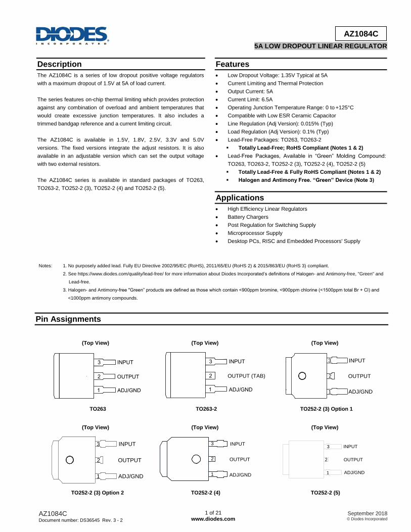
Pin Assignments
(Top View) (Top View) (Top View)
TO263 TO263-2 TO252-2 (3) Option 1
(Top View) (Top View) (Top View)
TO252-2 (3) Option 2 TO252-2 (4) TO252-2 (5)
1
2
3 INPUT
OUTPUT
ADJ/GND
INPUT
OUTPUT (TAB)
ADJ/GND1
2
3
1
2
3 INPUT
OUTPUT
ADJ/GND
1
2
3 INPUT
OUTPUT
ADJ/GND
1
2
3 INPUT
OUTPUT
ADJ/GND1
2
3 INPUT
OUTPUT
ADJ/GND
AZ1084C Document number: DS36545 Rev. 3 - 2
2 of 21 www.diodes.com
September 2018 © Diodes Incorporated
AZ1084C
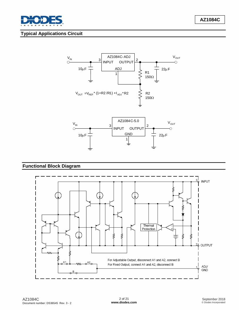
Typical Applications Circuit
AZ1084C-ADJ
INPUT OUTPUT
ADJ
VIN
R2
VIN
AZ1084C-5.0
INPUT OUTPUT
GND
VOUT
VOUT
R1
VOUT =VREF
* (1+R2 /R1) + IADJ * R2
150
150
22F10F
22F10F
3 2
1
3 2
1
Functional Block Diagram
AZ1084C Document number: DS36545 Rev. 3 - 2
3 of 21 www.diodes.com
September 2018 © Diodes Incorporated
AZ1084C
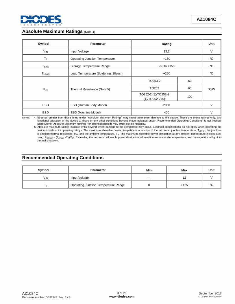
Absolute Maximum Ratings (Note 4)
Symbol Parameter Rating Unit
VIN Input Voltage 13.2 V
TJ Operating Junction Temperature +150 °C
TSTG Storage Temperature Range -65 to +150 °C
TLEAD Lead Temperature (Soldering, 10sec.) +260 °C
θJA Thermal Resistance (Note 5)
TO263-2 60
°C/W TO263 60
TO252-2 (3)/TO252-2
(4)/TO252-2 (5) 100
ESD ESD (Human Body Model) 2000 V
ESD ESD (Machine Model) 400 V
Notes: 4. Stresses greater than those listed under “Absolute Maximum Ratings” may cause permanent damage to the device. These are stress ratings only, and functional operation of the device at these or any other conditions beyond those indicated under “Recommended Operating Conditions” is not implied. Exposure to “Absolute Maximum Ratings” for extended periods may affect device reliability.
5. Absolute maximum ratings indicate limits beyond which damage to the component may occur. Electrical specifications do not apply when operating the
device outside of its operating ratings. The maximum allowable power dissipation is a function of the maximum junction temperature, TJ(max), the junction-
to-ambient thermal resistance, θJA, and the ambient temperature, TA. The maximum allowable power dissipation at any ambient temperature is calculated
using: PD(max) = (TJ(max) -TA)/θJA. Exceeding the maximum allowable power dissipation will result in excessive die temperature, and the regulator will go into
thermal shutdown.
Recommended Operating Conditions
Symbol Parameter Min Max Unit
VIN Input Voltage — 12 V
TJ Operating Junction Temperature Range 0 +125 °C
AZ1084C Document number: DS36545 Rev. 3 - 2
4 of 21 www.diodes.com
September 2018 © Diodes Incorporated
AZ1084C
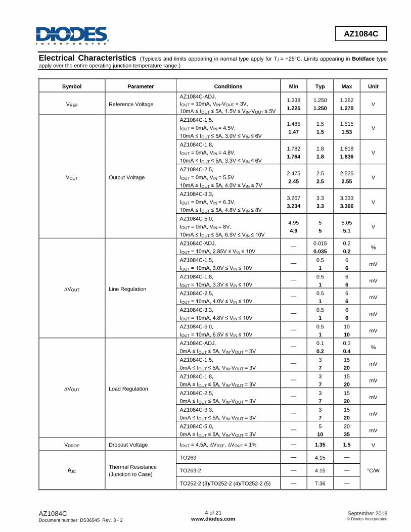
Electrical Characteristics (Typicals and limits appearing in normal type apply for TJ = +25°C. Limits appearing in Boldface type
apply over the entire operating junction temperature range.)
Symbol Parameter Conditions Min Typ Max Unit
VREF Reference Voltage
AZ1084C-ADJ,
IOUT = 10mA, VIN-VOUT = 3V,
10mA ≤ IOUT ≤ 5A, 1.5V ≤ VIN-VOUT ≤ 5V
1.238
1.225
1.250
1.250
1.262
1.270 V
VOUT Output Voltage
AZ1084C-1.5,
IOUT = 0mA, VIN = 4.5V,
10mA ≤ IOUT ≤ 5A, 3.0V ≤ VIN ≤ 6V
1.485
1.47
1.5
1.5
1.515
1.53 V
AZ1084C-1.8,
IOUT = 0mA, VIN = 4.8V,
10mA ≤ IOUT ≤ 5A, 3.3V ≤ VIN ≤ 6V
1.782
1.764
1.8
1.8
1.818
1.836 V
AZ1084C-2.5,
IOUT = 0mA, VIN = 5.5V
10mA ≤ IOUT ≤ 5A, 4.0V ≤ VIN ≤ 7V
2.475
2.45
2.5
2.5
2.525
2.55 V
AZ1084C-3.3,
IOUT = 0mA, VIN = 6.3V,
10mA ≤ IOUT ≤ 5A, 4.8V ≤ VIN ≤ 8V
3.267
3.234
3.3
3.3
3.333
3.366 V
AZ1084C-5.0,
IOUT = 0mA, VIN = 8V,
10mA ≤ IOUT ≤ 5A, 6.5V ≤ VIN ≤ 10V
4.95
4.9
5
5
5.05
5.1 V
∆VOUT Line Regulation
AZ1084C-ADJ,
IOUT = 10mA, 2.85V ≤ VIN ≤ 10V —
0.015
0.035
0.2
0.2 %
AZ1084C-1.5,
IOUT = 10mA, 3.0V ≤ VIN ≤ 10V —
0.5
1
6
6 mV
AZ1084C-1.8,
IOUT = 10mA, 3.3V ≤ VIN ≤ 10V —
0.5
1
6
6 mV
AZ1084C-2.5,
IOUT = 10mA, 4.0V ≤ VIN ≤ 10V —
0.5
1
6
6 mV
AZ1084C-3.3,
IOUT = 10mA, 4.8V ≤ VIN ≤ 10V —
0.5
1
6
6 mV
AZ1084C-5.0,
IOUT = 10mA, 6.5V ≤ VIN ≤ 10V —
0.5
1
10
10 mV
∆VOUT Load Regulation
AZ1084C-ADJ,
0mA ≤ IOUT ≤ 5A, VIN-VOUT = 3V —
0.1
0.2
0.3
0.4 %
AZ1084C-1.5,
0mA ≤ IOUT ≤ 5A, VIN-VOUT = 3V —
3
7
15
20 mV
AZ1084C-1.8,
0mA ≤ IOUT ≤ 5A, VIN-VOUT = 3V —
3
7
15
20 mV
AZ1084C-2.5,
0mA ≤ IOUT ≤ 5A, VIN-VOUT = 3V —
3
7
15
20 mV
AZ1084C-3.3,
0mA ≤ IOUT ≤ 5A, VIN-VOUT = 3V —
3
7
15
20 mV
AZ1084C-5.0,
0mA ≤ IOUT ≤ 5A, VIN-VOUT = 3V —
5
10
20
35 mV
VDROP Dropout Voltage IOUT = 4.5A, ∆VREF, ∆VOUT = 1% — 1.35 1.5 V
θJC
Thermal Resistance
(Junction to Case)
TO263 — 4.15 —
°C/W TO263-2 — 4.15 —
TO252-2 (3)/TO252-2 (4)/TO252-2 (5) — 7.36 —
AZ1084C Document number: DS36545 Rev. 3 - 2
5 of 21 www.diodes.com
September 2018 © Diodes Incorporated
AZ1084C
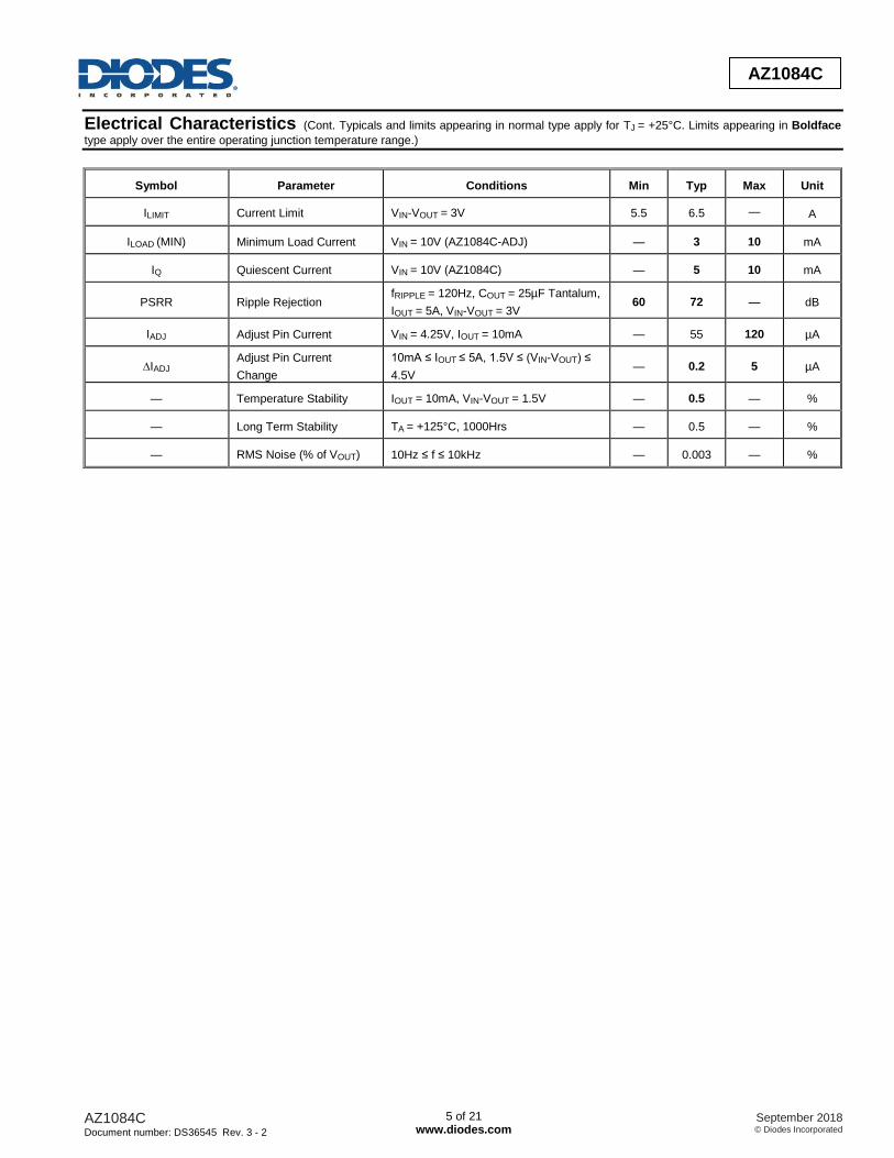
Electrical Characteristics (Cont. Typicals and limits appearing in normal type apply for TJ = +25°C. Limits appearing in Boldface
type apply over the entire operating junction temperature range.)
Symbol Parameter Conditions Min Typ Max Unit
ILIMIT Current Limit VIN-VOUT = 3V 5.5 6.5 — A
ILOAD (MIN) Minimum Load Current VIN = 10V (AZ1084C-ADJ) — 3 10 mA
IQ Quiescent Current VIN = 10V (AZ1084C) — 5 10 mA
PSRR Ripple Rejection fRIPPLE = 120Hz, COUT = 25µF Tantalum,
IOUT = 5A, VIN-VOUT = 3V 60 72 — dB
IADJ Adjust Pin Current VIN = 4.25V, IOUT = 10mA — 55 120 µA
∆IADJ
Adjust Pin Current
Change
10mA ≤ IOUT ≤ 5A, 1.5V ≤ (VIN-VOUT) ≤
4.5V — 0.2 5 µA
— Temperature Stability IOUT = 10mA, VIN-VOUT = 1.5V — 0.5 — %
— Long Term Stability TA = +125°C, 1000Hrs — 0.5 — %
— RMS Noise (% of VOUT) 10Hz ≤ f ≤ 10kHz — 0.003 — %
AZ1084C Document number: DS36545 Rev. 3 - 2
6 of 21 www.diodes.com
September 2018 © Diodes Incorporated
AZ1084C
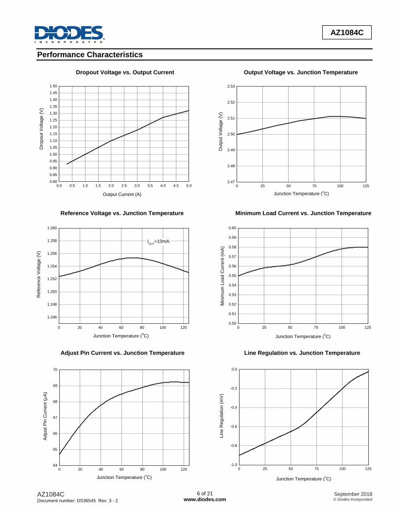
Performance Characteristics
Dropout Voltage vs. Output Current Output Voltage vs. Junction Temperature
Reference Voltage vs. Junction Temperature Minimum Load Current vs. Junction Temperature
Adjust Pin Current vs. Junction Temperature Line Regulation vs. Junction Temperature
0.0 0.5 1.0 1.5 2.0 2.5 3.0 3.5 4.0 4.5 5.00.80
0.85
0.90
0.95
1.00
1.05
1.10
1.15
1.20
1.25
1.30
1.35
1.40
1.45
1.50
Dro
po
ut V
olta
ge
(V
)
Output Current (A)
0 25 50 75 100 1252.47
2.48
2.49
2.50
2.51
2.52
2.53
Ou
tpu
t V
olta
ge
(V
)
Junction Temperature (oC)
0 20 40 60 80 100 120
1.246
1.248
1.250
1.252
1.254
1.256
1.258
1.260
Re
fere
nce
Vo
lta
ge
(V
)
Junction Temperature (oC)
IOUT
=10mA
0 25 50 75 100 1250.50
0.51
0.52
0.53
0.54
0.55
0.56
0.57
0.58
0.59
0.60
M
inim
um
Lo
ad
Cu
rre
nt (m
A)
Junction Temperature (0C)
0 20 40 60 80 100 12064
65
66
67
68
69
70
Ad
just P
in C
urr
en
t (
A)
Junction Temperature (oC)
0 25 50 75 100 125-1.0
-0.8
-0.6
-0.4
-0.2
0.0
Lin
e R
eg
ula
tio
n (
mV
)
Junction Temperature (oC)
AZ1084C Document number: DS36545 Rev. 3 - 2
7 of 21 www.diodes.com
September 2018 © Diodes Incorporated
AZ1084C
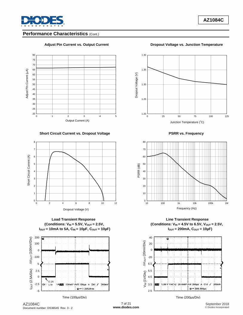
Performance Characteristics (Cont.)
Adjust Pin Current vs. Output Current Dropout Voltage vs. Junction Temperature
Short Circuit Current vs. Dropout Voltage PSRR vs. Frequency
Load Transient Response Line Transient Response
(Conditions: VIN = 5.5V, VOUT = 2.5V, (Conditions: VIN = 4.5V to 6.5V, VOUT = 2.5V,
IOUT = 10mA to 5A, CIN = 10µF, COUT = 10µF) IOUT = 200mA, COUT = 10µF)
I OU
T (2.5
A/D
iv)
∆V
OU
T (100m
V/D
iv)
Time (100µs/Div)
0.1A
VIN
(1V
/Div
) ∆
VO
UT
(20m
V/D
iv)
Time (200µs/Div)
0 1 2 3 4 520
25
30
35
40
45
50
55
60
65
70
75
80
Ad
just P
in C
urr
en
t (
A)
Output Current (A)
0 25 50 75 100 1251.20
1.25
1.30
1.35
1.40
Dro
po
ut V
olta
ge
(V
)
Junction Temperature (oC)
0 2 4 6 8 10 120
1
2
3
4
5
6
7
8
Sh
ort
Cir
cu
it C
urr
en
t (A
)
Dropout Voltage (V)
10 100 1k 10k 100k 1M0
10
20
30
40
50
60
70
80
P
SR
R (
dB
)
Frequency (Hz)
200
100
0
-100
5
2.5
0
-2.5
-5
40
20
0
-20
6.5
5.5
4.5
3.5
2.5
AZ1084C Document number: DS36545 Rev. 3 - 2
8 of 21 www.diodes.com
September 2018 © Diodes Incorporated
AZ1084C
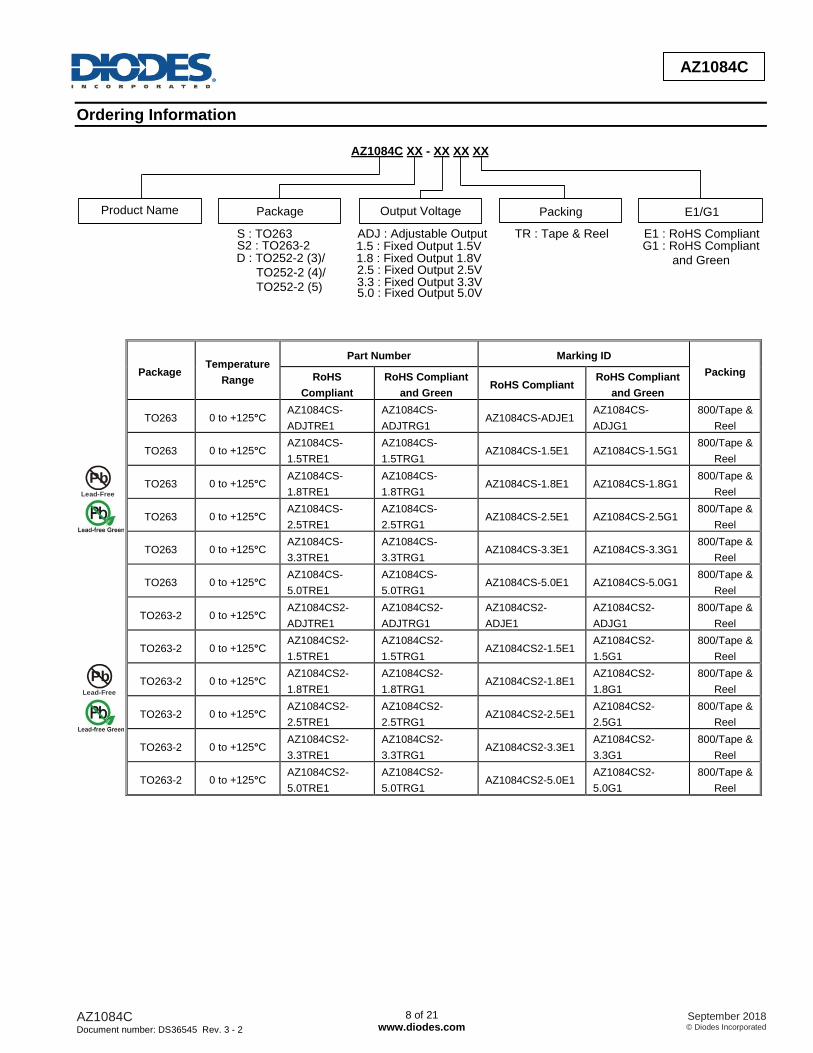
Ordering Information
AZ1084C XX - XX XX XX
PackingPackage
TR : Tape & ReelS : TO263S2 : TO263-2
Product Name E1/G1
D : TO252-2 (3)/
TO252-2 (4)/
TO252-2 (5)
E1 : RoHS Compliant
Output Voltage
ADJ : Adjustable Output1.5 : Fixed Output 1.5V1.8 : Fixed Output 1.8V2.5 : Fixed Output 2.5V3.3 : Fixed Output 3.3V5.0 : Fixed Output 5.0V
G1 : RoHS Compliant
and Green
Package Temperature
Range
Part Number Marking ID
Packing RoHS
Compliant
RoHS Compliant
and Green RoHS Compliant
RoHS Compliant
and Green
TO263 0 to +125°C
AZ1084CS-
ADJTRE1
AZ1084CS-
ADJTRG1 AZ1084CS-ADJE1
AZ1084CS-
ADJG1
800/Tape &
Reel
TO263 0 to +125°C
AZ1084CS-
1.5TRE1
AZ1084CS-
1.5TRG1 AZ1084CS-1.5E1 AZ1084CS-1.5G1
800/Tape &
Reel
TO263 0 to +125°C
AZ1084CS-
1.8TRE1
AZ1084CS-
1.8TRG1 AZ1084CS-1.8E1 AZ1084CS-1.8G1
800/Tape &
Reel
TO263 0 to +125°C
AZ1084CS-
2.5TRE1
AZ1084CS-
2.5TRG1 AZ1084CS-2.5E1 AZ1084CS-2.5G1
800/Tape &
Reel
TO263 0 to +125°C
AZ1084CS-
3.3TRE1
AZ1084CS-
3.3TRG1 AZ1084CS-3.3E1 AZ1084CS-3.3G1
800/Tape &
Reel
TO263 0 to +125°C
AZ1084CS-
5.0TRE1
AZ1084CS-
5.0TRG1 AZ1084CS-5.0E1 AZ1084CS-5.0G1
800/Tape &
Reel
TO263-2 0 to +125°C
AZ1084CS2-
ADJTRE1
AZ1084CS2-
ADJTRG1
AZ1084CS2-
ADJE1
AZ1084CS2-
ADJG1
800/Tape &
Reel
TO263-2 0 to +125°C
AZ1084CS2-
1.5TRE1
AZ1084CS2-
1.5TRG1 AZ1084CS2-1.5E1
AZ1084CS2-
1.5G1
800/Tape &
Reel
TO263-2 0 to +125°C
AZ1084CS2-
1.8TRE1
AZ1084CS2-
1.8TRG1 AZ1084CS2-1.8E1
AZ1084CS2-
1.8G1
800/Tape &
Reel
TO263-2 0 to +125°C
AZ1084CS2-
2.5TRE1
AZ1084CS2-
2.5TRG1 AZ1084CS2-2.5E1
AZ1084CS2-
2.5G1
800/Tape &
Reel
TO263-2 0 to +125°C
AZ1084CS2-
3.3TRE1
AZ1084CS2-
3.3TRG1 AZ1084CS2-3.3E1
AZ1084CS2-
3.3G1
800/Tape &
Reel
TO263-2 0 to +125°C
AZ1084CS2-
5.0TRE1
AZ1084CS2-
5.0TRG1 AZ1084CS2-5.0E1
AZ1084CS2-
5.0G1
800/Tape &
Reel
PbLead-Free
PbLead-Free
AZ1084C Document number: DS36545 Rev. 3 - 2
9 of 21 www.diodes.com
September 2018 © Diodes Incorporated
AZ1084C
Ordering Information (Cont.)
Package Temperature
Range
Part Number Marking ID
Packing RoHS
Compliant
RoHS
Compliant and
Green
RoHS
Compliant
RoHS
Compliant
and Green
TO252-2 (3)/(4)/(5) 0 to +125°C —
AZ1084CD-
ADJTRG1 —
AZ1084CD-
ADJG1
2500/Tape &
Reel
TO252-2 (3)/(4)/(5) 0 to +125°C —
AZ1084CD-
1.5TRG1 —
AZ1084CD-
1.5G1
2500/Tape &
Reel
TO252-2 (3)/(4)/(5) 0 to +125°C —
AZ1084CD-
1.8TRG1 —
AZ1084CD-
1.8G1
2500/Tape &
Reel
TO252-2 (3)/(4)/(5) 0 to +125°C —
AZ1084CD-
2.5TRG1 —
AZ1084CD-
2.5G1
2500/Tape &
Reel
TO252-2 (3)/(4)/(5) 0 to +125°C —
AZ1084CD-
3.3TRG1 —
AZ1084CD-
3.3G1
2500/Tape &
Reel
TO252-2 (3)/(4)/(5) 0 to +125°C —
AZ1084CD-
5.0TRG1 —
AZ1084CD-
5.0G1
2500/Tape &
Reel
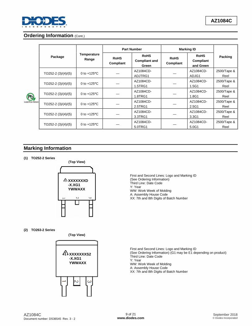
Marking Information (1) TO252-2 Series
(Top View)
(2) TO263-2 Series
(Top View)
XXXXXXXD -X.XG1 YWWAXX
First and Second Lines: Logo and Marking ID (See Ordering Information) Third Line: Date Code Y: Year WW: Work Week of Molding A: Assembly House Code XX: 7th and 8th Digits of Batch Number
XXXXXXXS2 -X.XG1
YWWAXX
First and Second Lines: Logo and Marking ID (See Ordering Information) (G1 may be E1 depending on product) Third Line: Date Code Y: Year WW: Work Week of Molding A: Assembly House Code XX: 7th and 8th Digits of Batch Number
AZ1084C Document number: DS36545 Rev. 3 - 2
10 of 21 www.diodes.com
September 2018 © Diodes Incorporated
AZ1084C
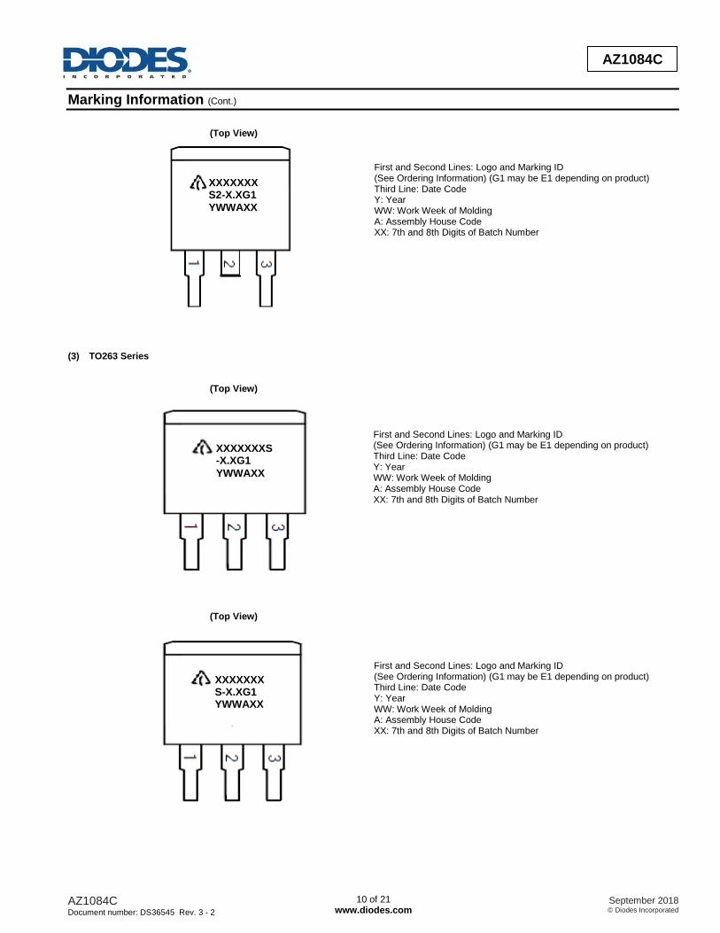
Marking Information (Cont.)
(Top View)
(3) TO263 Series
(Top View)
(Top View)
XXXXXXX S2-X.XG1
YWWAXX
XXXXXXXS -X.XG1
YWWAXX
XXXXXXX S-X.XG1 YWWAXX
First and Second Lines: Logo and Marking ID (See Ordering Information) (G1 may be E1 depending on product) Third Line: Date Code Y: Year WW: Work Week of Molding A: Assembly House Code XX: 7th and 8th Digits of Batch Number
First and Second Lines: Logo and Marking ID (See Ordering Information) (G1 may be E1 depending on product) Third Line: Date Code Y: Year WW: Work Week of Molding A: Assembly House Code XX: 7th and 8th Digits of Batch Number
First and Second Lines: Logo and Marking ID (See Ordering Information) (G1 may be E1 depending on product) Third Line: Date Code Y: Year WW: Work Week of Molding A: Assembly House Code XX: 7th and 8th Digits of Batch Number

AZ1084C Document number: DS36545 Rev. 3 - 2
11 of 21 www.diodes.com
September 2018 © Diodes Incorporated
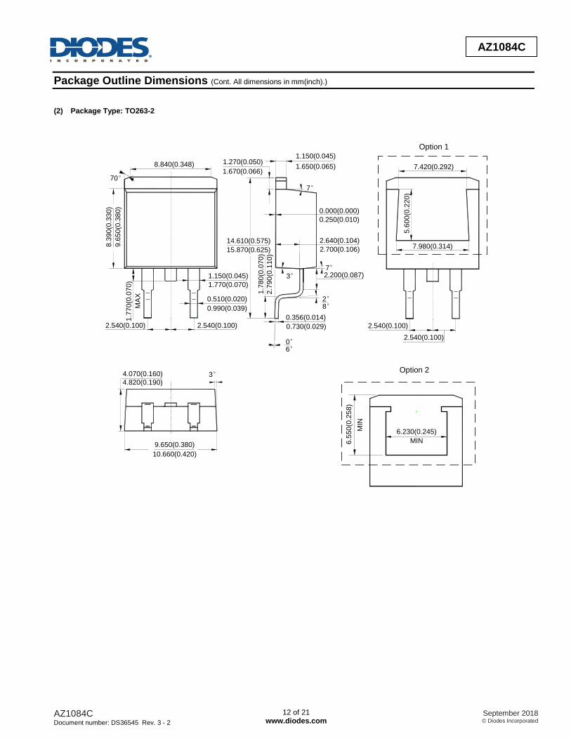
AZ1084C
Package Outline Dimensions (All dimensions in mm(inch).)
(1) Package Type: TO263
7°
3°7°
9.6
50
(0.3
80
)
0.990(0.039)
0.510(0.020)
2.540(0.100)
1.150(0.045)
9.650(0.380)
3°
14.760(0.581)
8.840(0.348)
2.640(0.104)
0.000(0.000)
8°2°
0°6°
2.200(0.087)
70°
4.070(0.160)
4.820(0.190)
1.150(0.045)
2.540(0.100)
1.270(0.050)
15.740(0.620)
0.250(0.010)
2.700(0.106)
5.6
00(0
.22
0)
7.420(0.292)
7.980(0.314)
2.540(0.100)
2.540(0.100)
10.660(0.420)
1.670(0.066)1.650(0.065)
1.770(0.070)
0.356(0.014)
0.730(0.029)
8.3
90
(0.3
30)
1.7
80(0
. 07
0)
2.7
90
(0. 1
10
)
Option 1
6.230(0.245)
MIN6.5
50
(0.2
58
)
MIN
Option 2
AZ1084C Document number: DS36545 Rev. 3 - 2
12 of 21 www.diodes.com
September 2018 © Diodes Incorporated
AZ1084C
Package Outline Dimensions (Cont. All dimensions in mm(inch).)
(2) Package Type: TO263-2
7°
3°7°
8.3
90(0
.33
0)
9.6
50
(0.3
80
)
0.990(0.039)
0.510(0.020)
2.540(0.100)
1.150(0.045)
9.650(0.380)
3°
14.610(0.575)
8.840(0.348)
2.640(0.104)
0.000(0.000)
8°2°
0°6°
0.356(0.014)
1.7
80
(0.0
70
)
2.200(0.087)
70°
10.660(0.420)
4.070(0.160)
4.820(0.190)
1.650(0.065)
1.150(0.045)
1.770(0.070)
2.540(0.100)
1.270(0.050)
1.670(0.066)
2.7
90(0
. 11
0)
15.870(0.625)
0.250(0.010)
2.700(0.106)
5.6
00
(0. 2
20)
7.420(0.292)
7.980(0.314)
2.540(0.100)
2.540(0.100)
1.7
70
(0.0
70)
MA
X
0.730(0.029)
6.230(0.245)
Option 1
MIN6.5
50
(0.2
58
)
MIN
Option 2
AZ1084C Document number: DS36545 Rev. 3 - 2
13 of 21 www.diodes.com
September 2018 © Diodes Incorporated
AZ1084C
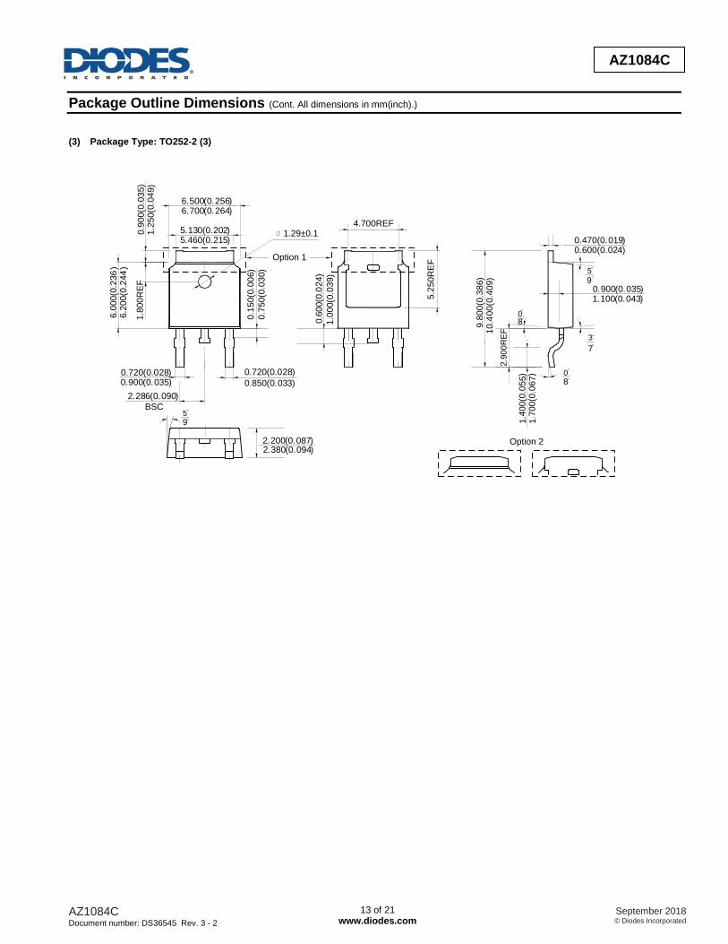
Package Outline Dimensions (Cont. All dimensions in mm(inch).)
(3) Package Type: TO252-2 (3)
1.29±0.1
2.9
00
RE
F
1.4
00(0
.055)
1.7
00(0
.067)
0.470(0.019)0.600(0.024)
5
9
089
.800(0
.38
6)
10.4
00(0
.409)
2.200(0.087)2.380(0.094)
0.900(0.035)1.100(0.043)
4.700REF
6.500(0.256)6.700(0.264)
5.130(0.202)5.460(0.215)
0.1
50(0
.00
6)
0.7
50(0
.03
0)
6.0
00(0
.236
)6.2
00(0
.244
)
0.720(0.028)
0.850(0.033)
2.286(0.090)
BSC
0.720(0.028)0.900(0.035)
0.9
00(0
.03
5)
1.2
50(0
.049)
1.8
00
RE
F
80
0.6
00(0
.02
4)
1.0
00(0
.039)
7
3
95
5.2
50
RE
F
Option 1
Option 2
AZ1084C Document number: DS36545 Rev. 3 - 2
14 of 21 www.diodes.com
September 2018 © Diodes Incorporated
AZ1084C
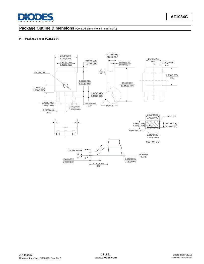
Package Outline Dimensions (Cont. All dimensions in mm(inch).)
(4) Package Type: TO252-2 (4)
5.460(0.215)
4.960(0.195)
6.350(0.250)
6.730(0.265)
1.20±0.05
1.900(0.075)
1.700(0.067)
6.220(0.245)
5.970(0.235)
1.270(0.050)
0.890(0.035)
1.492(0.059)
1.145(0.045)
1.010(0.040)1.124(0.044)
0.765(0.030)
2.290(0.090)
0.640(0.025)
0.884(0.035)
MAX
BSC
10.340(0.407)
9.940(0.391)
0.600(0.024)
0.460(0.018)
2.380(0.094)
2.180(0.086)
4.320(0.170)MIN
MIN
5.210(0.205)15
0
3 3
0.780(0.031)
0.650(0.026)
0.884(0.035)
0.640(0.025)
0.460(0.018)0.610(0.024)
0.410(0.016)
0.560(0.022)
DETAIL “A”
2.160(0.085)
MIN
BASE METAL
PLATING
SECTION B-B
0.020(0.001)
0.120(0.005)2.740(0.108)
1.500(0.059)
REF
1.780(0.070)
0
10
SEATING
PLANE
GAUGE PLANEB
B
AZ1084C Document number: DS36545 Rev. 3 - 2
15 of 21 www.diodes.com
September 2018 © Diodes Incorporated
AZ1084C
Package Outline Dimensions (Cont. All dimensions in mm(inch).)
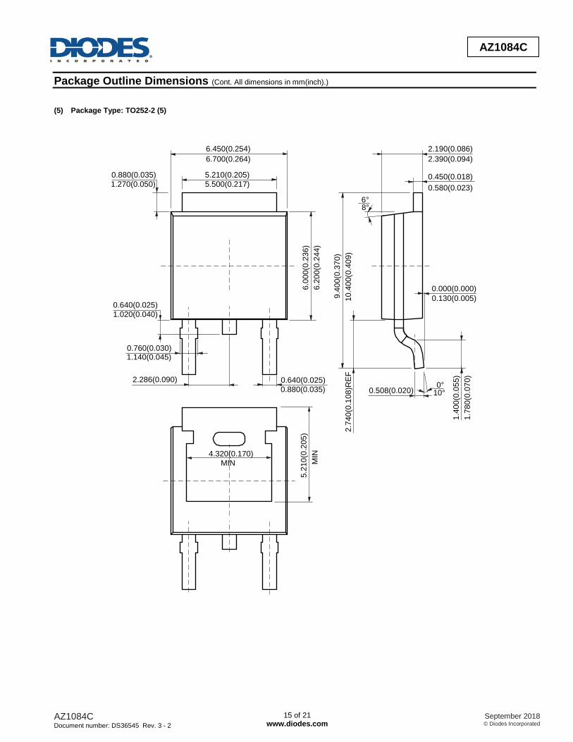
(5) Package Type: TO252-2 (5)
2.190(0.086)
2.390(0.094)
0.508(0.020)0°
10°
1.4
00
(0.0
55
)
1.7
80
(0.0
70
)
2.7
40
(0.1
08
)RE
F
9.4
00
(0.3
70
)
10
.40
0(0
.40
9)
0.000(0.000)
0.130(0.005)
6°8°
0.450(0.018)
0.580(0.023)
6.0
00
(0.2
36
)
6.2
00
(0.2
44
)
5.2
10(0
.20
5)
MIN4.320(0.170)
MIN
6.450(0.254)
6.700(0.264)
5.210(0.205)
5.500(0.217)
0.880(0.035)
1.270(0.050)
0.640(0.025)
1.020(0.040)
0.760(0.030)1.140(0.045)
2.286(0.090) 0.640(0.025)
0.880(0.035)
AZ1084C Document number: DS36545 Rev. 3 - 2
16 of 21 www.diodes.com
September 2018 © Diodes Incorporated
AZ1084C
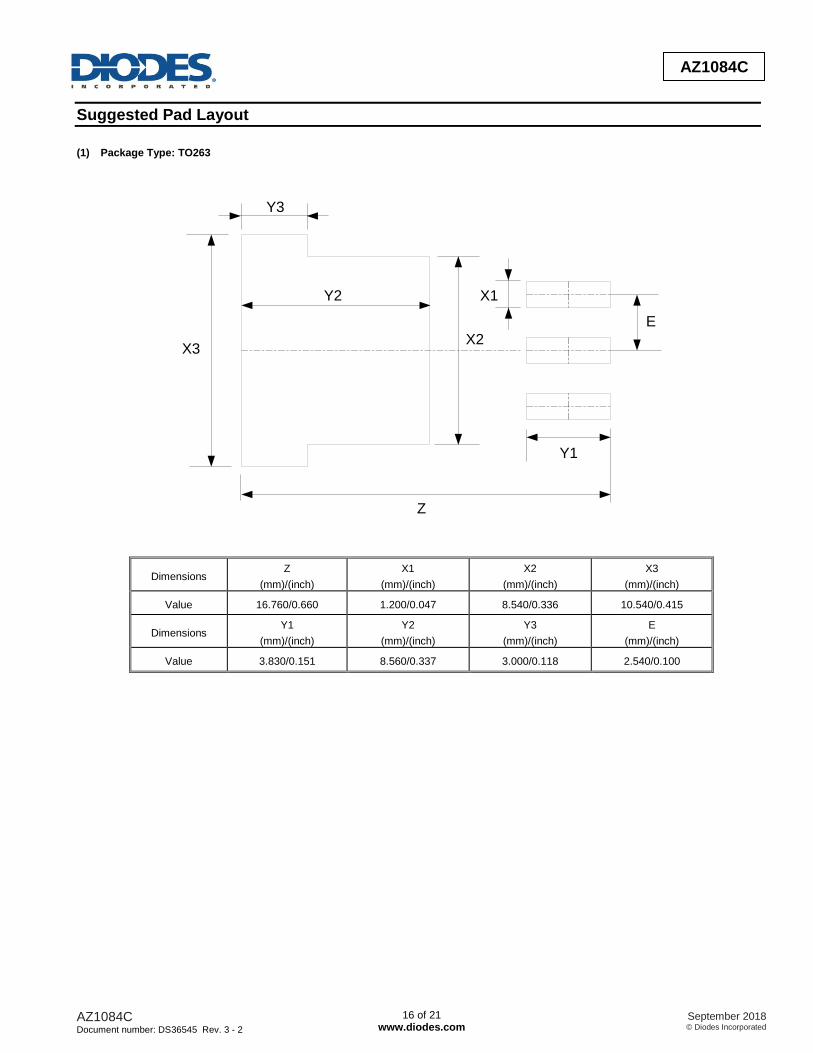
Suggested Pad Layout
(1) Package Type: TO263
Y3
Y2
X2
Z
X3
X1
E
Y1
Dimensions Z
(mm)/(inch)
X1
(mm)/(inch)
X2
(mm)/(inch)
X3
(mm)/(inch)
Value 16.760/0.660 1.200/0.047 8.540/0.336 10.540/0.415
Dimensions Y1
(mm)/(inch)
Y2
(mm)/(inch)
Y3
(mm)/(inch)
E
(mm)/(inch)
Value 3.830/0.151 8.560/0.337 3.000/0.118 2.540/0.100

AZ1084C Document number: DS36545 Rev. 3 - 2
17 of 21 www.diodes.com
September 2018 © Diodes Incorporated
AZ1084C
Suggested Pad Layout (Cont.)
(2) Package Type: TO263-2
Y3
Y2
X2
Z
X3
X1
E
Y1
Dimensions Z
(mm)/(inch)
X1
(mm)/(inch)
X2
(mm)/(inch)
X3
(mm)/(inch)
Value 16.760/0.660 1.200/0.047 8.540/0.336 10.540/0.415
Dimensions Y1
(mm)/(inch)
Y2
(mm)/(inch)
Y3
(mm)/(inch)
E
(mm)/(inch)
Value 3.830/0.151 8.560/0.337 3.000/0.118 5.080/0.200

AZ1084C Document number: DS36545 Rev. 3 - 2
18 of 21 www.diodes.com
September 2018 © Diodes Incorporated
AZ1084C
Suggested Pad Layout (Cont.)
(3) Package Type: TO252-2 (3)
E1X1
Y2
Y1
Z
X2
G
Dimensions Z
(mm)/(inch)
X1
(mm)/(inch)
X2=Y2
(mm)/(inch)
Y1
(mm)/(inch)
G
(mm)/(inch)
E1
(mm)/(inch)
Value 11.600/0.457 1.500/0.059 7.000/0.276 2.500/0.098 2.100/0.083 2.300/0.091
AZ1084C Document number: DS36545 Rev. 3 - 2
19 of 21 www.diodes.com
September 2018 © Diodes Incorporated
AZ1084C
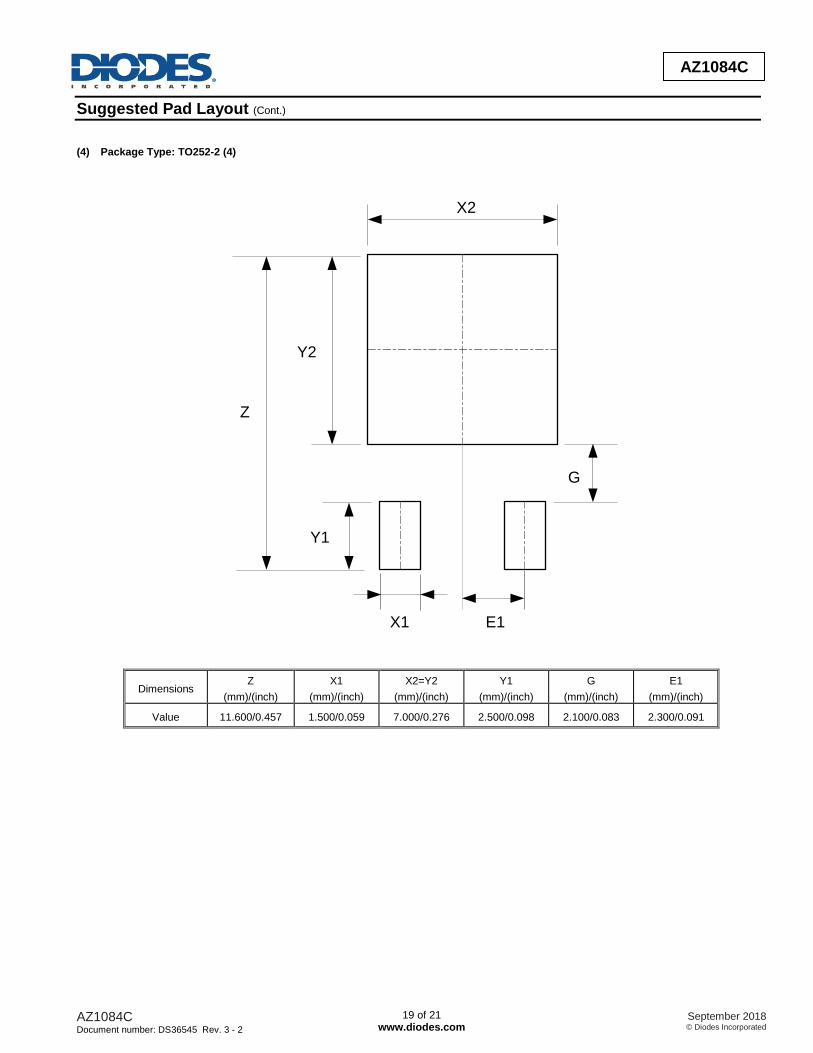
Suggested Pad Layout (Cont.)
(4) Package Type: TO252-2 (4)
E1X1
Y2
Y1
Z
X2
G
Dimensions Z
(mm)/(inch)
X1
(mm)/(inch)
X2=Y2
(mm)/(inch)
Y1
(mm)/(inch)
G
(mm)/(inch)
E1
(mm)/(inch)
Value 11.600/0.457 1.500/0.059 7.000/0.276 2.500/0.098 2.100/0.083 2.300/0.091
AZ1084C Document number: DS36545 Rev. 3 - 2
20 of 21 www.diodes.com
September 2018 © Diodes Incorporated
AZ1084C
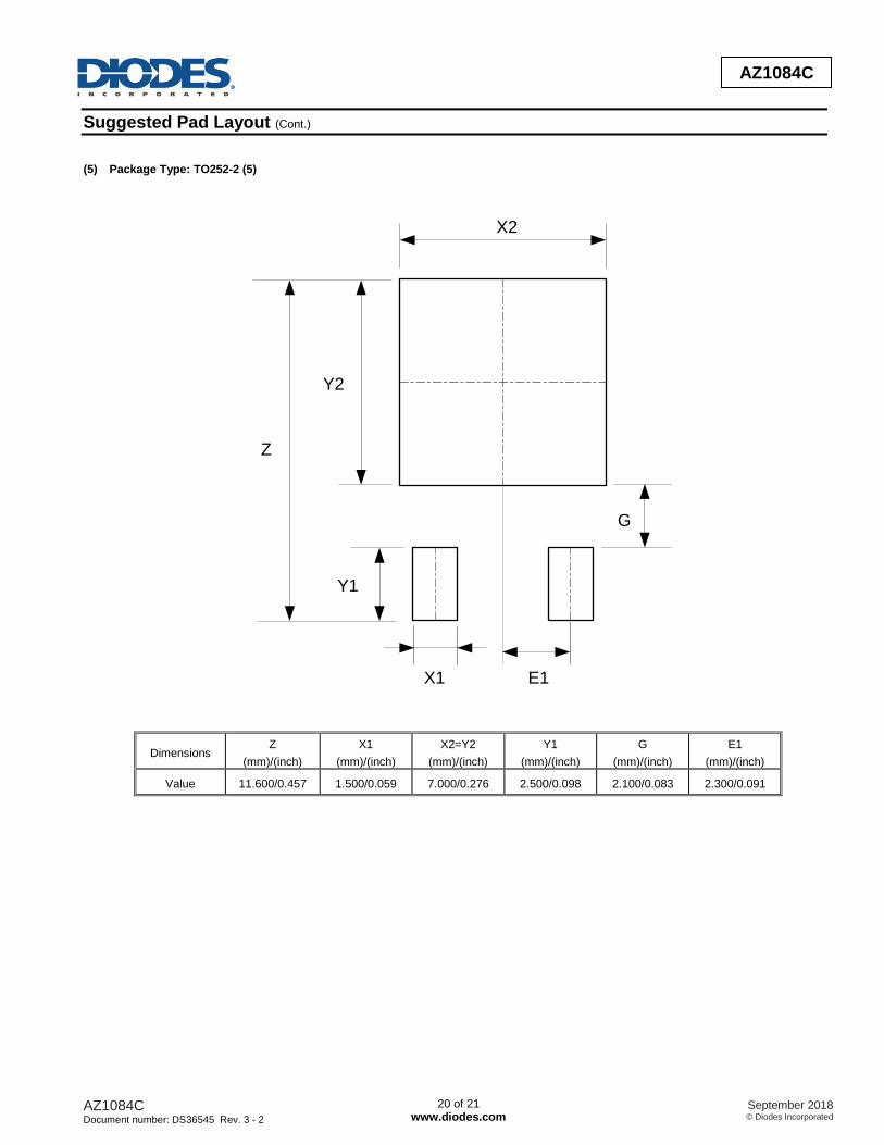
Suggested Pad Layout (Cont.)
(5) Package Type: TO252-2 (5)
E1X1
Y2
Y1
Z
X2
G
Dimensions Z
(mm)/(inch)
X1
(mm)/(inch)
X2=Y2
(mm)/(inch)
Y1
(mm)/(inch)
G
(mm)/(inch)
E1
(mm)/(inch)
Value 11.600/0.457 1.500/0.059 7.000/0.276 2.500/0.098 2.100/0.083 2.300/0.091
AZ1084C Document number: DS36545 Rev. 3 - 2
21 of 21 www.diodes.com
September 2018 © Diodes Incorporated
AZ1084C
IMPORTANT NOTICE DIODES INCORPORATED MAKES NO WARRANTY OF ANY KIND, EXPRESS OR IMPLIED, WITH REGARDS TO THIS DOCUMENT, INCLUDING, BUT NOT LIMITED TO, THE IMPLIED WARRANTIES OF MERCHANTABILITY AND FITNESS FOR A PARTICULAR PURPOSE (AND THEIR EQUIVALENTS UNDER THE LAWS OF ANY JURISDICTION). Diodes Incorporated and its subsidiaries reserve the right to make modifications, enhancements, improvements, corrections or other changes without further notice to this document and any product described herein. Diodes Incorporated does not assume any liability arising out of the application or use of this document or any product described herein; neither does Diodes Incorporated convey any license under its patent or trademark rights, nor the rights of others. Any Customer or user of this document or products described herein in such applications shall assume all risks of such use and will agree to hold Diodes Incorporated and all the companies whose products are represented on Diodes Incorporated website, harmless against all damages. Diodes Incorporated does not warrant or accept any liability whatsoever in respect of any products purchased through unauthorized sales channel. Should Customers purchase or use Diodes Incorporated products for any unintended or unauthorized application, Customers shall indemnify and hold Diodes Incorporated and its representatives harmless against all claims, damages, expenses, and attorney fees arising out of, directly or indirectly, any claim of personal injury or death associated with such unintended or unauthorized application. Products described herein may be covered by one or more United States, international or foreign patents pending. Product names and markings noted herein may also be covered by one or more United States, international or foreign trademarks. This document is written in English but may be translated into multiple languages for reference. Only the English version of this document is the final and determinative format released by Diodes Incorporated.
LIFE SUPPORT Diodes Incorporated products are specifically not authorized for use as critical components in life support devices or systems without the express written approval of the Chief Executive Officer of Diodes Incorporated. As used herein: A. Life support devices or systems are devices or systems which: 1. are intended to implant into the body, or
2. support or sustain life and whose failure to perform when properly used in accordance with instructions for use provided in the labeling can be reasonably expected to result in significant injury to the user.
B. A critical component is any component in a life support device or system whose failure to perform can be reasonably expected to cause the failure of the life support device or to affect its safety or effectiveness. Customers represent that they have all necessary expertise in the safety and regulatory ramifications of their life support devices or systems, and acknowledge and agree that they are solely responsible for all legal, regulatory and safety-related requirements concerning their products and any use of Diodes Incorporated products in such safety-critical, life support devices or systems, notwithstanding any devices- or systems-related information or support that may be provided by Diodes Incorporated. Further, Customers must fully indemnify Diodes Incorporated and its representatives against any damages arising out of the use of Diodes Incorporated products in such safety-critical, life support devices or systems. Copyright © 2018, Diodes Incorporated www.diodes.com