Embed Size (px)
Citation preview

AZ DISPLAYS,INC.
SPECIFICATIONS FOR
LIQUID CRYSTAL DISPLAY
@
PART NUMBER: AGM3224O Series
DATE: APRIL 06, 2007
COMPLETE LCD SOLUTIONS

1. FUNCTIONS & F EA TURES
Viewing Direction : 6 O’ clock
Driving Scheme : 1/240 Duty Cy cle, 1/17 Bi as
Display Content : 320*240 Dots
Power Supply Voltage : +5.0V
LCD Drivin g Voltage (V LCD =V DD-V 0) : 22.0V
Dot Size : 0.20(W)*0. 22(H)mm
Dot Gap : 0.01mm
2. BLOCK DIAGRAM
LCD PANEL320X240 Dots
SEG161~SEG320SEG1~SEG160
S6B0794 orTL0134F2
S6B0794 orTL0134F2
LED-(K)
LED+(A)
LP
MF
FLM
CP
DX0~DX3
COM1 .. ..COM240
BACKLIGHT
S6B0796 orTL0136F1Power
Supply
SED1335F
VSS
VDD
VDDH
DB0~DB7
A0
WR
/RD
/RES
/CS
32K RAM
AZ Displays, Inc. Page 01

3. EXTERNAL DIMENSIONS
AZ Displays, Inc. Page 02

4. PIN ASSIGNMENT
Pin No. Symbol Function
1 V SS Ground terminal of module
2 VDD Power terminal of module 2.7V to 5.5V (TYP: 5.0V)
3 VDDH Contrast voltage for LCD d rive (variable)
4 NC No used
5 /WR 8080family : Write signal; 6800 family : R/W signal
6 /RD 8080 family : Read signal; 6800 family : Enable clock (E)
7 /CS Chip select
8 A0 Data type select
9 /RES Reset
10~17 D B 0~DB 7 Data bus
18 N C No used
19 LED-(K) Cathode for backlight
20 LED +(A ) A node for backlight
5. BACKLIGHT
1. Electrical/Optical Sp ecifications & Package Dimensions :
Item Symbol MIN. TYP . MAX . Unit Conditions
Forward Voltage Vf --- 4.1 --- V
Forward Current If --- --- 100 mA Vf=4.1V
Power Dissipation Pd --- --- 0.41 W Vf=4.1V
Reverse Voltage VR --- 10 --- V
Reverse Current IR --- 0.20 --- mA
Luminous Intensity Iv --- 20 --- Cd/m2 Vf=4 .1V
Luminous Uniformity 70 --- --- % Vf=4.1V
Emission Wavelength p --- 572 --- nm
Spectral R ange --- --- --- nm
If=10mA Ta=25℃
Each chip
AZ Displays, Inc. Page 03
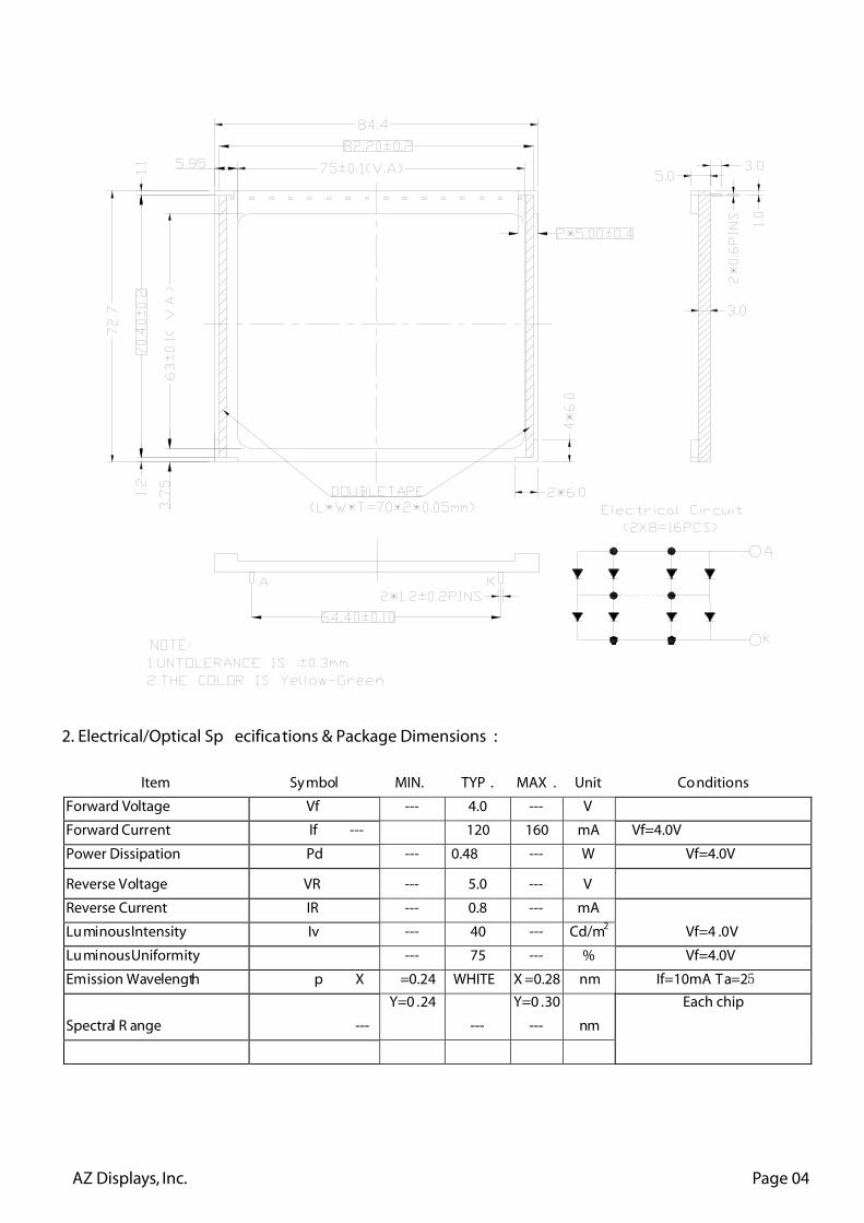
2. Electrical/Optical Sp ecifications & Package Dimensions :
Item Symbol MIN. TYP . MAX . Unit Conditions
Forward Voltage Vf --- 4.0 --- V
Forward Current If --- 120 160 mA Vf=4.0V
Power Dissipation Pd --- 0.48 --- W Vf=4.0V
Reverse Voltage VR --- 5.0 --- V
Reverse Current IR --- 0.8 --- mA
Luminous Intensity Iv --- 40 --- Cd/m2 Vf=4 .0V
Luminous Uniformity --- 75 --- % Vf=4.0V
Emission Wavelength p X =0.24
Y=0 .24
WHITE X =0.28
Y=0 .30
nm
Spectral R ange --- --- --- nm
If=10mA Ta=25℃
Each chip
AZ Displays, Inc. Page 04

MBG24001B 02, BACKLIGHT COLOR: WHITE
6. MAXIMUM ABSOLUTE LIMIT
Item Symbol Standard value Unit
Supply voltage range V DD -0.3~+7.0 V
Input voltage range V IN -0.3~V DD+0.3 V
Power supply for liquid crystal drive V DDH -0.3~+28 V
Voltage for BL V LED1 4~4 .5 V
Operating temperature range T opr 0~+50 ℃
Soldering temperature range Tstg -10~+60 ℃
AZ Displays, Inc. Page 05

7. ELECTRICAL CHARACTERISTICS VDD = 4 .5 to 5.5V, VSS = 0V , Ta = -10 to 60 unless otherwise noted.℃
Ra ting Parameter Symbol Condition
min typ max Unit
Supply voltage V DD 4.5 5.0 5.5 V
Register data retention voltage V OH 2.0 --- 6.0 V
Input leakage current ILI Vl=VDD. See note 5. --- 0.05 2.0 uA
Output leakage current I LO Vl=VSS. See note5. --- 0.10 5.0 uA
Operating supply current Iopr See note 4. --- 11 15 Ma
Quiescent supply current I Q
Sleep m ode,
Vosc1=V/CS=V/RD=VDD --- 0.05 20.0 uA
Oscilla tor frequency fOSC 1.0 --- 10.0 MHZ
External clock frequency fC1 1.0 --- 10.0 MHZ
Oscilla tor feedback resistance Rf
Measured at crystal, 47.5%
duty cycle. See note
6. 0.5 1.0 3.0 MΩ
TTL
HIGH-level input voltage V IH T See note 1. 0.5V DD V DD V
LOW -level input voltage V IL T See note 1. Vss 0.2V DD V
HIGH-level output voltage V OHT IOH=-5.0 mA . See note 1. 2.4 V
LO W-level output voltage V OLT I OL =5.0 mA . See note 1. Vss+0. 4 V
CMOS
HIGH-level input voltage V IHC See note 2. 0.8V DD V DD V
LOW -level input voltage V ILC See note 2. Vss 0.2V DD V
HIGH-level output voltage V OHC I OH=-2.0 mA . See note 2. V DD-0.4 V
LO W-level output voltage V OLC I OH=1.6 mA . See note 2. V ss+0.4 V
Open-drain
LO W-level output voltage V OLN IOL=6.0 mA --- --- Vss+0.4 V
Schmitt-trigger
Ri sing-edge threshold voltage V T+ See note 3. 0.5V DD 0.7V DD 0.8V DD V
Falling-edge threshold voltage V T- See note 3. 0.2V DD 0.3V DD 0.5V DD V Notes: 1. D0 to D 7, A0, /CS, /RD, /WR are TTL-level inputs.
2. SEL is CO MS-lev el inputs. YD, XD0 to XD3 , XSCL , LP , WF, YDIS are COMS-leve l output.
3. RES is a Schmitt-trigger input. The pulse width on RE S must be at least 200 us. Note that pulses of more than
a few seconds will cause DC v oltages to be applied to the LCD panel.
4. Fosc=10MHz , no l oad (no display memory), internal character generator, 256 x 200 pixel display. Th e
operating supply currentcan be reduced by approximately 1 mA by setting both CL O and the display OFF .
5. V D0 to V D7 and D0 to D7 have internal feedback circuits so that if the inputs become high-impedance, the
input state immediately prior to that is held. Bec ause of the feedback circuit, i nput current flow occurs when
the inputs are in an intermediate state.
6. B ecause the oscillator circuit input bias current is in the order of uA, design the printed so as to reduce leakage
currents.
AZ Displays, Inc. Page 06

8. SED1335F TIMING DIAGRAMS
8.1. 8080 Family Interface T iming
D0toD7
D0toD7
AO,/CS
/WR,/RD
Ta=-10 to 60℃ VDD=4 .5 to 5.5V VDD=2 .7 to 4.5V
Signal Symbol Parameter min max min max
Unit Conditi on
tAH8 Address hold time 10 - 10 - ns A0, CS
tAW 8 Address setup time 0 - 0 - ns
tCYC8 System cycle time See note. - See note. - ns WR, RD
tCC Strobe pulsewidth 120 - 150 - ns
tDS8 Data setup time 120 - 120 - ns tDH8 Data hold time 5 - 5 - ns tOH8 Output disable time 10 50 10 55 ns
D0 to D7
tACC8 RD access time - 50 - 80 ns
CL=1 00 pF
Note: For memory control and system control commands:
tCYC8 =2tC+tCC +tCEA +75>tACV +245
For all other commands:
tCYC8 =4tC+tCC +30
AZ Displays, Inc. Page 07

8-2. 6800 Family In terface timing
A0,CS
R/W
D0toD7
E
D0toD7
Note : tCYC 6 indicates the interval during which CS is LOW and E is HIGH .
Ta=-10 to 60℃ VDD=4 .5 to 5.5V VDD=2 .7 to 4.5V
Signal Symbol Parameter min max min max
Unit Conditi on
E t EW Enable pulsewidth 120 --- 150 --- ns
tAH6 Address hold time 0 - 10 - ns
tAW 6 Address setup time 0 - 0 - ns A0, CS
WR, RD tCYC6 System cycle time See note. - See note. - ns tDS6 Data setup time 120 - 120 - ns tDH6 Data hold time 5 - 5 - ns tOH6 Output disable time 10 50 10 55 ns
D0 to D7
tACC6 RD access time - 50 - 80 ns
CL=1 00 pF
Note: For memory control and system control commands:
tCYC6 =2tC+tEW +tCEA +75>tACV +245
For all other commands:
tCYC6 =4tC+tEW +30
8-3. Sleep in Command T iming
SYSTEM SET WRITESLEEP IN WRITE
(Command input)
YDIS
WR
VCE
AZ Displays, Inc. Page 08

Ta=-10 to 60 VDD=4 .5 to 5.5V VDD=2 .7 to 4.5V
Signal Symbol Parameter min max min max
Unit Conditi on
tWR D /VCE fa lling-edge delay time See note 1 --- See note 1 --- ns /WR
tWR L YDIS falling-ed ge delay time --- See note 2 --- See note 2 ns CL=1 00 pF
Notes: 1. Twrd=18tC+tOSS+40 (T oss is the time delay from the sleep state until stable operation)
2. Twrl=36tC*[TC /R]*[L/F]+70
9. INSTRUCTION SET
9.1. The Command Set Code Command command read
Descrip tion Paramet ers Class Command /RD /WR A 0 D7 D6 D5 D4 D3 D2 D1 D0
Hex
No. of B ytes Section
System Initia lize device and
control SYSTEM SET 1 0 1 0 1 0 0 0 0 0 0 40
display 8
S LEEP IN 1 0 1 0 1 0 1 0 0 1 1 53 Enter standby mode 0
DISP ON/OFF 58, Enable and disable display
1 0 1 0 1 0 1 1 0 0 D
59 and display flashing 1
Set display start address
SCROLL 1 0 1 0 1 0 0 0 1 0 0 44
and display regions 10
CSRFOR M 1 0 1 0 1 0 1 1 1 0 1 5D Set cursor type 2
Display Set start address of character
control CGRAM ADR 1 0 1 0 1 0 1 1 1 0 0 5C
generator RAM 2
CD CD 4C Set direction of cursor
CSRDIR
1 0 to movement
1 0 1 0 1 0 0 1 1
4F
0
Set horizontal scroll
HDOT SCR 1 0 1 0 1 0 1 1 0 1 0 5A
position 1
Set display overlay
OVLA Y 1 0 1 0 1 0 1 1 0 1 1 5B
format 1
Drawing CSR W 1 0 1 0 1 0 0 0 1 1 0 46 Set cursor address 2
control CSRR 1 0 1 0 1 0 0 0 1 1 1 47 Read cursor address 2
Memory MWRITE 1 0 1 0 1 0 0 0 0 1 0 42 Write to display memory --------
control Read from display
MREAD 1 0 1 0 1 0 0 0 0 1 1 43
memory --------
Notes: 1. In general, the internal registers of the SED1335 series are modified as each command parameter is input.
However, the microprocessor does not have to set all the parameters of a command and may send a new
command before all parameters have been input. Th e internal registers for the parameters that have been input
will have been changed but the remaining parameter registers are unchanged.
2-byte parameter (where two bytes are treated as 1 data item) are handled as follows:
a. CSR W, CSRR: E ach byte is processed individually. The microprocessor may read or write just the low byte of
the cursor address.
b. Sy stem Set, Scr oll , CGRAM ADR: Bo th parameter bytes are processed together. If the command is changed
after half of the parameter has been input, the single byte is i gnored.
2. A PL and A PH are 2-byte parameters, but are treated as two 1-byte parameters.
AZ Displays, Inc. Page 09