Embed Size (px)
Citation preview

AXI Memory Mapped to PCI Express (PCIe) Gen2 v2.8LogiCORE IP Product Guide
Vivado Design Suite
PG055 April 4, 2018
AXI Memory Mapped to PCIe Gen2 v2.8 2PG055 April 4, 2018 www.xilinx.com
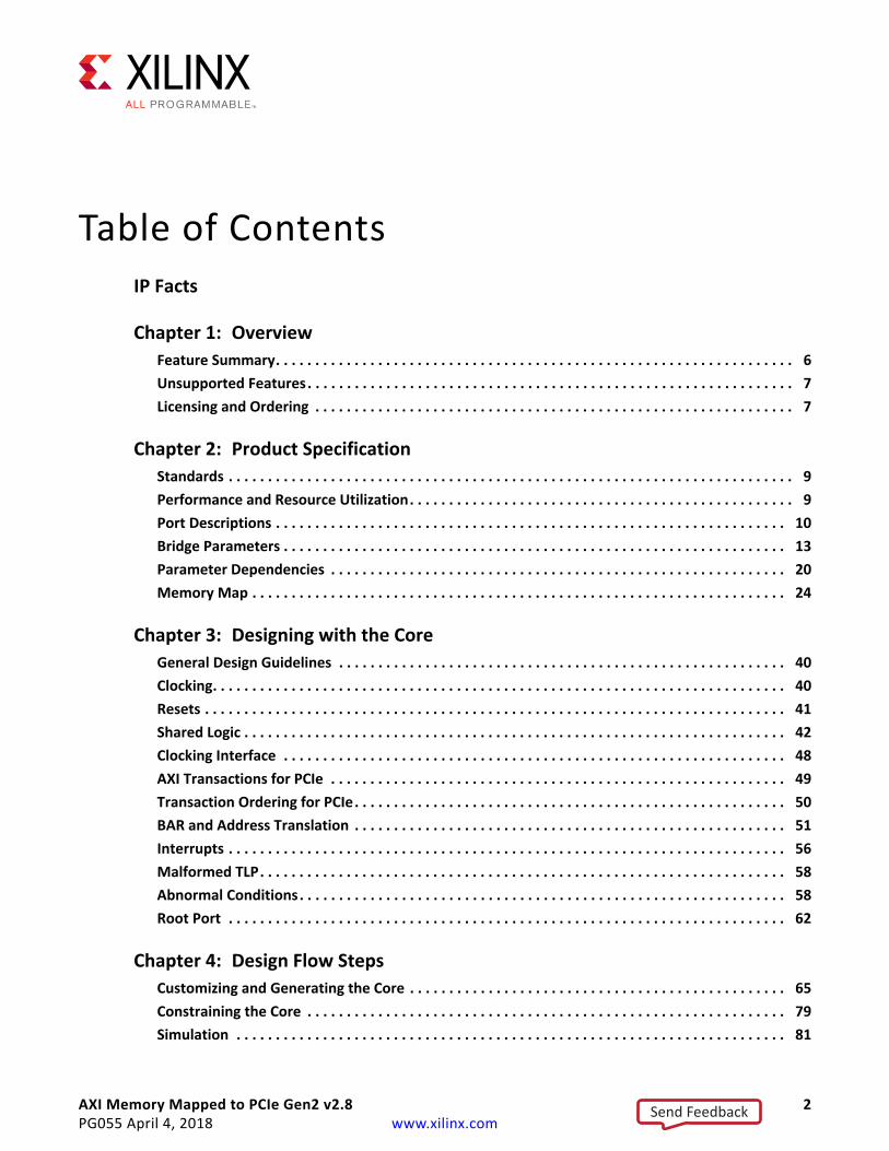
Table of ContentsIP Facts
Chapter 1: OverviewFeature Summary. . . . . . . . . . . . . . . . . . . . . . . . . . . . . . . . . . . . . . . . . . . . . . . . . . . . . . . . . . . . . . . . . . 6Unsupported Features. . . . . . . . . . . . . . . . . . . . . . . . . . . . . . . . . . . . . . . . . . . . . . . . . . . . . . . . . . . . . . 7Licensing and Ordering . . . . . . . . . . . . . . . . . . . . . . . . . . . . . . . . . . . . . . . . . . . . . . . . . . . . . . . . . . . . . 7
Chapter 2: Product SpecificationStandards . . . . . . . . . . . . . . . . . . . . . . . . . . . . . . . . . . . . . . . . . . . . . . . . . . . . . . . . . . . . . . . . . . . . . . . . 9Performance and Resource Utilization. . . . . . . . . . . . . . . . . . . . . . . . . . . . . . . . . . . . . . . . . . . . . . . . . 9Port Descriptions . . . . . . . . . . . . . . . . . . . . . . . . . . . . . . . . . . . . . . . . . . . . . . . . . . . . . . . . . . . . . . . . . 10Bridge Parameters . . . . . . . . . . . . . . . . . . . . . . . . . . . . . . . . . . . . . . . . . . . . . . . . . . . . . . . . . . . . . . . . 13Parameter Dependencies . . . . . . . . . . . . . . . . . . . . . . . . . . . . . . . . . . . . . . . . . . . . . . . . . . . . . . . . . . 20Memory Map . . . . . . . . . . . . . . . . . . . . . . . . . . . . . . . . . . . . . . . . . . . . . . . . . . . . . . . . . . . . . . . . . . . . 24
Chapter 3: Designing with the CoreGeneral Design Guidelines . . . . . . . . . . . . . . . . . . . . . . . . . . . . . . . . . . . . . . . . . . . . . . . . . . . . . . . . . 40Clocking. . . . . . . . . . . . . . . . . . . . . . . . . . . . . . . . . . . . . . . . . . . . . . . . . . . . . . . . . . . . . . . . . . . . . . . . . 40Resets . . . . . . . . . . . . . . . . . . . . . . . . . . . . . . . . . . . . . . . . . . . . . . . . . . . . . . . . . . . . . . . . . . . . . . . . . . 41Shared Logic . . . . . . . . . . . . . . . . . . . . . . . . . . . . . . . . . . . . . . . . . . . . . . . . . . . . . . . . . . . . . . . . . . . . . 42Clocking Interface . . . . . . . . . . . . . . . . . . . . . . . . . . . . . . . . . . . . . . . . . . . . . . . . . . . . . . . . . . . . . . . . 48AXI Transactions for PCIe . . . . . . . . . . . . . . . . . . . . . . . . . . . . . . . . . . . . . . . . . . . . . . . . . . . . . . . . . . 49Transaction Ordering for PCIe. . . . . . . . . . . . . . . . . . . . . . . . . . . . . . . . . . . . . . . . . . . . . . . . . . . . . . . 50BAR and Address Translation . . . . . . . . . . . . . . . . . . . . . . . . . . . . . . . . . . . . . . . . . . . . . . . . . . . . . . . 51Interrupts . . . . . . . . . . . . . . . . . . . . . . . . . . . . . . . . . . . . . . . . . . . . . . . . . . . . . . . . . . . . . . . . . . . . . . . 56Malformed TLP. . . . . . . . . . . . . . . . . . . . . . . . . . . . . . . . . . . . . . . . . . . . . . . . . . . . . . . . . . . . . . . . . . . 58Abnormal Conditions. . . . . . . . . . . . . . . . . . . . . . . . . . . . . . . . . . . . . . . . . . . . . . . . . . . . . . . . . . . . . . 58Root Port . . . . . . . . . . . . . . . . . . . . . . . . . . . . . . . . . . . . . . . . . . . . . . . . . . . . . . . . . . . . . . . . . . . . . . . 62
Chapter 4: Design Flow StepsCustomizing and Generating the Core . . . . . . . . . . . . . . . . . . . . . . . . . . . . . . . . . . . . . . . . . . . . . . . . 65Constraining the Core . . . . . . . . . . . . . . . . . . . . . . . . . . . . . . . . . . . . . . . . . . . . . . . . . . . . . . . . . . . . . 79Simulation . . . . . . . . . . . . . . . . . . . . . . . . . . . . . . . . . . . . . . . . . . . . . . . . . . . . . . . . . . . . . . . . . . . . . . 81
Send Feedback
AXI Memory Mapped to PCIe Gen2 v2.8 3PG055 April 4, 2018 www.xilinx.com
Chapter 5: Example DesignOverview . . . . . . . . . . . . . . . . . . . . . . . . . . . . . . . . . . . . . . . . . . . . . . . . . . . . . . . . . . . . . . . . . . . . . . . 84Simulation Design Overview . . . . . . . . . . . . . . . . . . . . . . . . . . . . . . . . . . . . . . . . . . . . . . . . . . . . . . . . 84Implementation Design Overview . . . . . . . . . . . . . . . . . . . . . . . . . . . . . . . . . . . . . . . . . . . . . . . . . . . 86Example Design Elements . . . . . . . . . . . . . . . . . . . . . . . . . . . . . . . . . . . . . . . . . . . . . . . . . . . . . . . . . . 87Example Design Output Structure . . . . . . . . . . . . . . . . . . . . . . . . . . . . . . . . . . . . . . . . . . . . . . . . . . . 87
Chapter 6: Test BenchRoot Port Model Test Bench for Endpoint . . . . . . . . . . . . . . . . . . . . . . . . . . . . . . . . . . . . . . . . . . . . . 89Endpoint Model Test Bench for Root Port . . . . . . . . . . . . . . . . . . . . . . . . . . . . . . . . . . . . . . . . . . . . . 91
Appendix A: UpgradingMigrating to the Vivado Design Suite. . . . . . . . . . . . . . . . . . . . . . . . . . . . . . . . . . . . . . . . . . . . . . . . . 93Upgrading in the Vivado Design Suite . . . . . . . . . . . . . . . . . . . . . . . . . . . . . . . . . . . . . . . . . . . . . . . . 93
Appendix B: DebuggingFinding Help on Xilinx.com . . . . . . . . . . . . . . . . . . . . . . . . . . . . . . . . . . . . . . . . . . . . . . . . . . . . . . . . . 95Debug Tools . . . . . . . . . . . . . . . . . . . . . . . . . . . . . . . . . . . . . . . . . . . . . . . . . . . . . . . . . . . . . . . . . . . . . 96Simulation Debug. . . . . . . . . . . . . . . . . . . . . . . . . . . . . . . . . . . . . . . . . . . . . . . . . . . . . . . . . . . . . . . . 101Hardware Debug . . . . . . . . . . . . . . . . . . . . . . . . . . . . . . . . . . . . . . . . . . . . . . . . . . . . . . . . . . . . . . . . 103Interface Debug . . . . . . . . . . . . . . . . . . . . . . . . . . . . . . . . . . . . . . . . . . . . . . . . . . . . . . . . . . . . . . . . . 113
Appendix C: Additional Resources and Legal NoticesXilinx Resources . . . . . . . . . . . . . . . . . . . . . . . . . . . . . . . . . . . . . . . . . . . . . . . . . . . . . . . . . . . . . . . . . 114Documentation Navigator and Design Hubs . . . . . . . . . . . . . . . . . . . . . . . . . . . . . . . . . . . . . . . . . . 114References . . . . . . . . . . . . . . . . . . . . . . . . . . . . . . . . . . . . . . . . . . . . . . . . . . . . . . . . . . . . . . . . . . . . . 114Revision History . . . . . . . . . . . . . . . . . . . . . . . . . . . . . . . . . . . . . . . . . . . . . . . . . . . . . . . . . . . . . . . . . 115Please Read: Important Legal Notices . . . . . . . . . . . . . . . . . . . . . . . . . . . . . . . . . . . . . . . . . . . . . . . 118
Send Feedback
AXI Memory Mapped to PCIe Gen2 v2.8 4PG055 April 4, 2018 www.xilinx.com Product Specification
IntroductionThe Xilinx® AXI Memory Mapped to PCI Express® core is an interface between AXI4 and PCI Express.
Features• Zynq®-7000 All Programmable SoC,
Virtex®-7, Kintex®-7, and Artix®-7 FPGA Integrated Blocks for PCI Express(3)
• Maximum Payload Size (MPS) up to 256 bytes• Multiple Vector Messaged Signaled Interrupts
(MSIs)• Legacy interrupt support• Memory-mapped AXI4 access to PCIe® space• PCIe access to memory-mapped AXI4 space• Tracks and manages Transaction Layer Packets
(TLPs) completion processing• Detects and indicates error conditions with
interrupts• Optimal AXI4 pipeline support for enhanced
performance• Compliant with Advanced RISC Machine
(ARM®) Advanced Microcontroller Bus Architecture 4 (AMBA®) AXI4 specification
• Supports up to three PCIe 32-bit or 64-bit PCIe Base Address Registers (BARs) as Endpoint
• Supports a single PCIe 32-bit or 64-bit BAR as Root Port
IP Facts
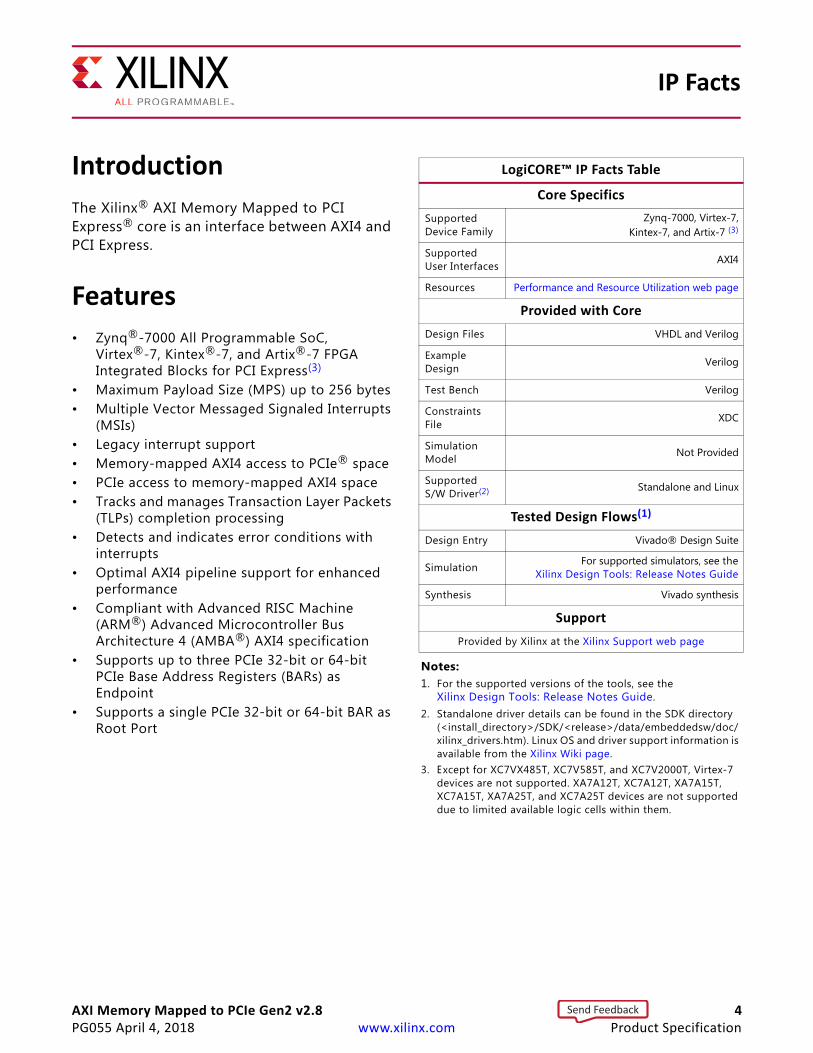
LogiCORE™ IP Facts Table
Core SpecificsSupported Device Family
Zynq-7000, Virtex-7,Kintex-7, and Artix-7 (3)
Supported User Interfaces AXI4
Resources Performance and Resource Utilization web page
Provided with CoreDesign Files VHDL and Verilog
Example Design Verilog
Test Bench Verilog
Constraints File XDC
Simulation Model Not Provided
Supported S/W Driver(2) Standalone and Linux
Tested Design Flows(1)
Design Entry Vivado® Design Suite
Simulation For supported simulators, see theXilinx Design Tools: Release Notes Guide
Synthesis Vivado synthesis
SupportProvided by Xilinx at the Xilinx Support web page
Notes: 1. For the supported versions of the tools, see the
Xilinx Design Tools: Release Notes Guide.2. Standalone driver details can be found in the SDK directory
(<install_directory>/SDK/<release>/data/embeddedsw/doc/xilinx_drivers.htm). Linux OS and driver support information is available from the Xilinx Wiki page.
3. Except for XC7VX485T, XC7V585T, and XC7V2000T, Virtex-7 devices are not supported. XA7A12T, XC7A12T, XA7A15T, XC7A15T, XA7A25T, and XC7A25T devices are not supported due to limited available logic cells within them.
Send Feedback

AXI Memory Mapped to PCIe Gen2 v2.8 5PG055 April 4, 2018 www.xilinx.com
Chapter 1
OverviewThe AXI Memory Mapped to PCI Express core is designed for the Vivado® IP integrator in the Vivado Design Suite. The AXI Memory Mapped to PCI Express core provides an interface between an AXI4 customer user interface and PCI Express using the Xilinx® Integrated Block for PCI Express. The AXI Memory Mapped to PCI Express core provides the translation level between the AXI4 embedded system to the PCI Express system. The AXI Memory Mapped to PCI Express core translates the AXI4 memory read or writes to PCIe Transaction Layer Packets (TLP) packets and translates PCIe memory read and write request TLP packets to AXI4 interface commands.
The architecture of the AXI Memory Mapped to PCI Express is shown in Figure 1-1.
Send Feedback

AXI Memory Mapped to PCIe Gen2 v2.8 6PG055 April 4, 2018 www.xilinx.com
Chapter 1: Overview
Feature SummaryThe AXI Memory Mapped to PCI Express core is an interface between the AXI4 and PCI Express. It contains the memory mapped AXI4 to AXI4-Stream Bridge and the AXI4-Stream Enhanced Interface Block for PCIe. The memory-mapped AXI4 to AXI4-Stream Bridge contains a register block and two functional half bridges, referred to as the Slave Bridge and Master Bridge. The slave bridge connects to the AXI4 Interconnect as a slave device to handle any issued AXI4 master read or write requests. The master bridge connects to the AXI4 Interconnect as a master to process the PCIe generated read or write TLPs. The core uses a set of interrupts to detect and flag error conditions.
The AXI Memory Mapped to PCI Express core supports both Root Port and Endpoint configurations.
• When configured as an Endpoint, the AXI Memory Mapped to PCI Express core supports up to three 32-bit or 64-bit PCIe Base Address Registers (BARs).
X-Ref Target - Figure 1-1
Figure 1-1: High-Level AXI Memory Mapped to PCI Express Architecture
AXI MM/S Bridge
Master Bridge
AXI PCIe Bridge
Slave Bridge
AXI-SEnhanced PCIe
IntegratedBlock
For PCIe
AXI4-Lite I/F
AXIMaster
I/F
AXI4MemoryMapped
Bus AXISlave
I/F
AXI MM (S_AXI_CTL)
PCIe Rx
PCIe Tx
AXI MM(S_AXI)
AXI MM(M_AXI)
Register Block
X12310
Send Feedback
AXI Memory Mapped to PCIe Gen2 v2.8 7PG055 April 4, 2018 www.xilinx.com
Chapter 1: Overview
• When configured as a Root Port, the core supports a single 32-bit or 64-bit PCIe BAR.
The AXI Memory Mapped to PCI Express core is compliant with the PCI Express Base Specification v2.0 [Ref 8] and with the AMBA® AXI Protocol Specification [Ref 7].
Unsupported FeaturesThe following features are not supported in the AXI Memory Mapped to PCI Express core.
• Tandem PROM and Tandem PCIe
• Advanced Error Reporting (AER)
• MSI-X
The PCIe transactions that can be generated are those that are compatible with the AXI4 specification. lists the supported PCIe transaction types.
Licensing and OrderingThis Xilinx LogiCORE™ IP module is provided at no additional cost with the Xilinx® Vivado® Design Suite under the terms of the Xilinx End User License.
For more information, visit the AXI Memory Mapped to PCI Express (PCIe) Gen2 product page.
Information about other Xilinx LogiCORE IP modules is available at the Xilinx Intellectual Property page. For information on pricing and availability of other Xilinx LogiCORE IP modules and tools, contact your local Xilinx sales representative.
Send Feedback
AXI Memory Mapped to PCIe Gen2 v2.8 8PG055 April 4, 2018 www.xilinx.com
Chapter 2
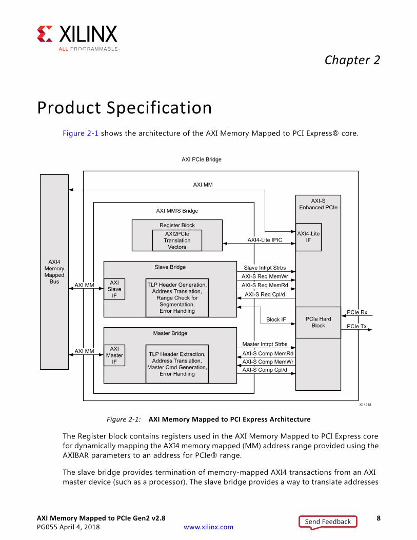
Product SpecificationFigure 2-1 shows the architecture of the AXI Memory Mapped to PCI Express® core.
The Register block contains registers used in the AXI Memory Mapped to PCI Express core for dynamically mapping the AXI4 memory mapped (MM) address range provided using the AXIBAR parameters to an address for PCIe® range.
The slave bridge provides termination of memory-mapped AXI4 transactions from an AXI master device (such as a processor). The slave bridge provides a way to translate addresses
X-Ref Target - Figure 2-1
Figure 2-1: AXI Memory Mapped to PCI Express Architecture
Register Block
Master Bridge
AXI PCIe Bridge
Slave Bridge
AXI-S Enhanced PCIe
PCIe Hard Block
AXI4-Lite IF
AXISlave
IF
AXIMaster
IF
AXI4MemoryMapped
Bus
AXI2PCIe Translation
Vectors
TLP Header Generation, Address Translation,
Range Check for Segmentation, Error Handling
TLP Header Extraction, Address Translation,
Master Cmd Generation,Error Handling
AXI MM/S Bridge
AXI MM
AXI4-Lite IPIC
Slave Intrpt StrbsAXI-S Req MemWrAXI-S Req MemRd
AXI-S Req Cpl/d
Block IF
Master Intrpt Strbs
AXI-S Comp MemRdAXI-S Comp MemWrAXI-S Comp Cpl/d
PCIe Rx
PCIe Tx
AXI MM
AXI MM
X14215
Send Feedback
AXI Memory Mapped to PCIe Gen2 v2.8 9PG055 April 4, 2018 www.xilinx.com
Chapter 2: Product Specification
that are mapped within the AXI4 memory mapped address domain to the domain addresses for PCIe. When a remote AXI master initiates a write transaction to the slave bridge, the write address and qualifiers are captured and write data is queued in a first in first out (FIFO). These are then converted into one or more MemWr TLPs, depending on the configured Max Payload Size setting, which are passed to the integrated block for PCI Express. The Slave Bridge can support up to two active AXI4 memory mapped write transactions.
When a remote AXI master initiates a read transaction to the slave bridge, the read address and qualifiers are captured and a MemRd request TLP is passed to the core and a completion timeout timer is started. Completions received through the core are correlated with pending read requests and read data is returned to the AXI master. The slave bridge is capable of handling up to eight memory mapped AXI4 read requests with pending completions.
The master bridge processes both PCIe MemWr and MemRd request TLPs received from the integrated block for PCI Express and provides a means to translate addresses that are mapped within the address for PCIe domain to the memory mapped AXI4 address domain. Each PCIe MemWr request TLP header is used to create an address and qualifiers for the memory mapped AXI4 bus and the associated write data is passed to the addressed memory mapped AXI4 Slave. The master bridge can support up to four active PCIe MemWr request TLPs.
Each PCIe MemRd request TLP header is used to create an address and qualifiers for the memory-mapped AXI4 bus. Read data is collected from the addressed memory mapped AXI4 Slave and used to generate completion TLPs which are then passed to the integrated block for PCI Express. The master bridge can handle up to four read requests with pending completions for improved AXI4 pipelining performance.
The instantiated AXI4-Stream Enhanced PCIe block contains submodules including the Requester/Completer interfaces to the AXI bridge and the Register block. The Register block contains the status, control, interrupt registers, and the AXI4-Lite interface.
StandardsThe AXI Memory Mapped to PCI Express core is compliant with the AMBA® AXI Protocol Specification [Ref 7] and the PCI Express Base Specification v2.0 [Ref 8].
Performance and Resource UtilizationFor full details about performance and resource utilization, visit the Performance and Resource Utilization web page.
Send Feedback
AXI Memory Mapped to PCIe Gen2 v2.8 10PG055 April 4, 2018 www.xilinx.com
Chapter 2: Product Specification
Port DescriptionsThe interface signals for the AXI Memory Mapped to PCI Express are described in Table 2-1.
Table 2-1: Top-Level Interface Signals
Signal Name I/O Description
Global Signals
refclk I PCIe Reference Clock
axi_aresetn I Global reset signal for the IP. Resets GT, PCIe, and AXI interfaces.
axi_aclk_out O PCIe derived clock output for axi_aclk.
axi_ctl_aclk_out O PCIe derived clock output for axi_ctl_aclk
mmcm_lock O Indicates axi_aclk_out from the axi_enhanced_pcie block is stable
interrupt_out O
Interrupt signal. This signal is asserted for as long as there exists at least one bit asserted in the Interrupt Decode register and is not masked in the Interrupt Mask register.
AXI Slave Interface
s_axi_awid[c_s_axi_id_width-1:0] I Slave write address ID
s_axi_awaddr[c_s_axi_addr_width-1:0] I Slave write address
s_axi_awregion[3:0] I Slave write region decode
s_axi_awlen[7:0] I Slave write burst length
s_axi_awsize[2:0] I Slave write burst size
s_axi_awburst[1:0] I Slave write burst type
s_axi_awvalid I Slave address write valid
s_axi_awready O Slave address write ready
s_axi_wdata[c_s_axi_data_width-1:0] I Slave write data
s_axi_wstrb[c_s_axi_data_width/8-1:0] I Slave write strobe
s_axi_wlast I Slave write last
s_axi_wvalid I Slave write valid
s_axi_wready O Slave write ready
s_axi_bid[c_s_axi_id_width-1:0] O Slave response ID
s_axi_bresp[1:0] O Slave write response
s_axi_bvalid O Slave write response valid
s_axi_bready I Slave response ready
s_axi_arid[c_s_axi_id_width-1:0] I Slave read address ID
s_axi_araddr[c_s_axi_addr_width-1:0] I Slave read address
Send Feedback

AXI Memory Mapped to PCIe Gen2 v2.8 11PG055 April 4, 2018 www.xilinx.com
Chapter 2: Product Specification
s_axi_arregion[3:0] I Slave read region decode
s_axi_arlen[7:0] I Slave read burst length
s_axi_arsize[2:0] I Slave read burst size
s_axi_arburst[1:0] I Slave read burst type
s_axi_arvalid I Slave read address valid
s_axi_arready O Slave read address ready
s_axi_rid[c_s_axi_id_width-1:0] O Slave read ID tag
s_axi_rdata[c_s_axi_data_width-1:0] O Slave read data
s_axi_rresp[1:0] O Slave read response
s_axi_rlast O Slave read last
s_axi_rvalid O Slave read valid
s_axi_rready I Slave read ready
AXI Master Interface
m_axi_awaddr[c_m_axi_addr_width-1:0] O Master write address
m_axi_awlen[7:0] O Master write burst length
m_axi_awsize[2:0] O Master write burst size
m_axi_awburst[1:0] O Master write burst type
m_axi_awprot[2:0] O Master write protection type
m_axi_awvalid O Master write address valid
m_axi_awready I Master write address ready
m_axi_wdata[c_m_axi_data_width-1:0] O Master write data
m_axi_wstrb[c_m_axi_data_width/8-1:0] O Master write strobe
m_axi_wlast O Master write last
m_axi_wvalid O Master write valid
m_axi_wready I Master write ready
m_axi_bresp[1:0] I Master write response
m_axi_bvalid I Master write response valid
m_axi_bready O Master response ready
m_axi_araddr[c_m_axi_addr_width-1:0] O Master read address
m_axi_arlen[7:0] O Master read burst length
m_axi_arsize[2:0](1) O Master read burst size
m_axi_arburst[1:0] O Master read burst type
m_axi_arprot[2:0] O Master read protection type
m_axi_arvalid O Master read address valid
Table 2-1: Top-Level Interface Signals (Cont’d)
Signal Name I/O Description
Send Feedback
AXI Memory Mapped to PCIe Gen2 v2.8 12PG055 April 4, 2018 www.xilinx.com
Chapter 2: Product Specification
m_axi_arready IMaster read address ready. This signal only responds when Bus Master Enable bit is set in the Command register within PCI Configuration Space.
m_axi_rdata[c_m_axi_data_width-1:0] I Master read data
m_axi_rresp[1:0] I Master read response
m_axi_rlast I Master read last
m_axi_rvalid I Master read valid
m_axi_rready O Master read ready
AXI4-Lite Control Interface
s_axi_ctl_awaddr[31:0] I Slave write address
s_axi_ctl_awvalid I Slave write address valid
s_axi_ctl_awready O Slave write address ready
s_axi_ctl_wdata[31:0] I Slave write data
s_axi_ctl_wstrb[3:0] I Slave write strobe
s_axi_ctl_wvalid I Slave write valid
s_axi_ctl_wready O Slave write ready
s_axi_ctl_bresp[1:0] O Slave write response
s_axi_ctl_bvalid O Slave write response valid
s_axi_ctl_bready I Slave response ready
s_axi_ctl_araddr[31:0] I Slave read address
s_axi_ctl_arvalid I Slave read address valid
s_axi_ctl_arready O Slave read address ready
s_axi_ctl_rdata[31:0] O Slave read data
s_axi_ctl_rresp[1:0] O Slave read response
s_axi_ctl_rvalid O Slave read valid
s_axi_ctl_rready I Slave read ready
MSI Signals
intx_msi_request I
Legacy interrupt input (see c_interrupt_pin) when msi_enable = 0.
Initiates a MSI write request when msi_enable = 1.
Intx_msi_request is asserted for one clock period.
intx_msi_grant OIndicates legacy interrupt/MSI grant signal. The intx_msi_grant signal is asserted for one clock period when the interrupt is accepted by the PCIe core.
msi_enable O Indicates when MSI is enabled.
msi_vector_num [4:0] I Indicates MSI vector to send when writing a MSI write request.
Table 2-1: Top-Level Interface Signals (Cont’d)
Signal Name I/O Description
Send Feedback
AXI Memory Mapped to PCIe Gen2 v2.8 13PG055 April 4, 2018 www.xilinx.com
Chapter 2: Product Specification
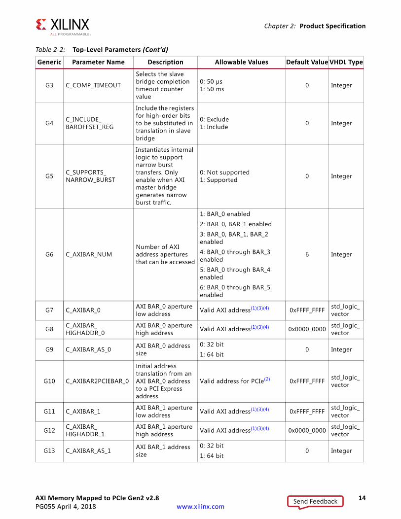
Bridge ParametersBecause many features in the AXI Memory Mapped to PCI Express core design can be parameterized, you can uniquely tailor the implementation of the core using only the resources required for the desired functionality. This approach also achieves the best possible performance with the lowest resource usage.
The parameters defined for the AXI Memory Mapped to PCI Express are shown in Table 2-2.
msi_vector_width [2:0] O Indicates the size of the MSI field (the number of MSI vectors allocated to the device).
PCIe Interface
pci_exp_rxp[C_NO_OF_LANES-1:0][] I PCIe RX serial interface
pci_exp_rxn[C_NO_OF_LANES-1:0][] I PCIe RX serial interface
pci_exp_txp[C_NO_OF_LANES-1:0][] O PCIe TX serial interface
pci_exp_txn[C_NO_OF_LANES-1:0][] O PCIe TX serial interface
Notes: 1. When a read request is received with a length that is not 1DW and is shorter than the Master AXI data width, m_axi_arsize
always indicates that the requested size is equal to the Master AXI data width. The core drops the extra data when a completion packet is formed and sent back to the requester.
Table 2-1: Top-Level Interface Signals (Cont’d)
Signal Name I/O Description
Table 2-2: Top-Level Parameters
Generic Parameter Name Description Allowable Values Default Value VHDL TypeBridge Parameters
C_PCIE_BLK_LOCNPCIe integrated block location within FPGA
0: X0Y0
1: X0Y1
2: X0Y2
3: X1Y0
4: X1Y1
0 String
C_XLNX_REF_BOARD Target FPGA Board
NONE
KC705_REVA
KC705_REVB
KC705_REVC
VC707
NONE String
G1 C_FAMILY Target FPGA Family kintex7, virtex7, artix7, zynq String
G2 C_INCLUDE_RC
Configures the AXI bridge for PCIe to be a Root Port or an Endpoint
0: Endpoint1: Root Port (applies only for 7 series, and Zynq-7000 AP SoC devices)
0 Integer
Send Feedback
AXI Memory Mapped to PCIe Gen2 v2.8 14PG055 April 4, 2018 www.xilinx.com
Chapter 2: Product Specification
G3 C_COMP_TIMEOUT
Selects the slave bridge completion timeout counter value
0: 50 µs1: 50 ms 0 Integer
G4 C_INCLUDE_BAROFFSET_REG
Include the registers for high-order bits to be substituted in translation in slave bridge
0: Exclude1: Include 0 Integer
G5 C_SUPPORTS_NARROW_BURST
Instantiates internal logic to support narrow burst transfers. Only enable when AXI master bridge generates narrow burst traffic.
0: Not supported1: Supported 0 Integer
G6 C_AXIBAR_NUMNumber of AXI address apertures that can be accessed
1: BAR_0 enabled
2: BAR_0, BAR_1 enabled
3: BAR_0, BAR_1, BAR_2 enabled
4: BAR_0 through BAR_3 enabled
5: BAR_0 through BAR_4 enabled
6: BAR_0 through BAR_5 enabled
6 Integer
G7 C_AXIBAR_0 AXI BAR_0 aperture low address Valid AXI address(1)(3)(4) 0xFFFF_FFFF std_logic_
vector
G8 C_AXIBAR_HIGHADDR_0
AXI BAR_0 aperture high address Valid AXI address(1)(3)(4) 0x0000_0000 std_logic_
vector
G9 C_AXIBAR_AS_0 AXI BAR_0 address size
0: 32 bit
1: 64 bit0 Integer
G10 C_AXIBAR2PCIEBAR_0
Initial address translation from an AXI BAR_0 address to a PCI Express address
Valid address for PCIe(2) 0xFFFF_FFFF std_logic_vector
G11 C_AXIBAR_1 AXI BAR_1 aperture low address Valid AXI address(1)(3)(4) 0xFFFF_FFFF std_logic_
vector
G12 C_AXIBAR_HIGHADDR_1
AXI BAR_1 aperture high address Valid AXI address(1)(3)(4) 0x0000_0000 std_logic_
vector
G13 C_AXIBAR_AS_1 AXI BAR_1 address size
0: 32 bit
1: 64 bit0 Integer
Table 2-2: Top-Level Parameters (Cont’d)
Generic Parameter Name Description Allowable Values Default Value VHDL Type
Send Feedback

AXI Memory Mapped to PCIe Gen2 v2.8 15PG055 April 4, 2018 www.xilinx.com
Chapter 2: Product Specification
G14 C_AXIBAR2PCIEBAR_1
Initial address translation from an AXI BAR_1 address to a PCI Express address
Valid address for PCIe(2) 0xFFFF_FFFF std_logic_vector
G15 C_AXIBAR_2 AXI BAR_2 aperture low address
Valid AXI address(1)(3)(4)0xFFFF_FFFF std_logic_
vector
G16 C_AXIBAR_HIGHADDR_2
AXI BAR_2 aperture high address
Valid AXI address(1)(3)(4)0x0000_0000 std_logic_
vector
G17 C_AXIBAR_AS_2 AXI BAR_2 address size
0: 32 bit
1: 64 bit0 Integer
G18 C_AXIBAR2PCIEBAR_2
Initial address translation from an AXI BAR_2 address to a PCI Express address
Valid address for PCIe(2) 0xFFFF_FFFF std_logic_vector
G19 C_AXIBAR_3 AXI BAR_3 aperture low address
Valid AXI address(1)(3)(4)0xFFFF_FFFF std_logic_
vector
G20 C_AXIBAR_HIGHADDR_3
AXI BAR_3 aperture high address
Valid AXI address(1)(3)(4)0x0000_0000 std_logic_
vector
G21 C_AXIBAR_AS_3 AXI BAR_3 address size
0: 32 bit
1: 64 bit0 Integer
G22 C_AXIBAR2PCIEBAR_3
Initial address translation from an AXI BAR_3 address to a PCI Express address
Valid address for PCIe(2) 0xFFFF_FFFF std_logic_vector
G23 C_AXIBAR_4 AXI BAR_4 aperture low address
Valid AXI address(1)(3)(4)0xFFFF_FFFF std_logic_
vector
G24 C_AXIBAR_HIGHADDR_4
AXI BAR_4 aperture high address
Valid AXI address(1)(3)(4)0x0000_0000 std_logic_
vector
G25 C_AXIBAR_AS_4 AXI BAR_4 address size
0: 32 bit
1: 64 bit0 Integer
G26 C_AXIBAR2PCIEBAR_4
Initial address translation from an AXI BAR_4 address to a PCI Express address
Valid address for PCIe(2) 0xFFFF_FFFF std_logic_vector
G27 C_AXIBAR_5 AXI BAR_5 aperture low address
Valid AXI address(1)(3)(4)0xFFFF_FFFF std_logic_
vector
Table 2-2: Top-Level Parameters (Cont’d)
Generic Parameter Name Description Allowable Values Default Value VHDL Type
Send Feedback
AXI Memory Mapped to PCIe Gen2 v2.8 16PG055 April 4, 2018 www.xilinx.com
Chapter 2: Product Specification
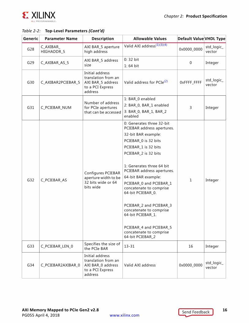
G28 C_AXIBAR_HIGHADDR_5
AXI BAR_5 aperture high address
Valid AXI address(1)(3)(4)0x0000_0000 std_logic_
vector
G29 C_AXIBAR_AS_5 AXI BAR_5 address size
0: 32 bit
1: 64 bit0 Integer
G30 C_AXIBAR2PCIEBAR_5
Initial address translation from an AXI BAR_5 address to a PCI Express address
Valid address for PCIe(2) 0xFFFF_FFFF std_logic_vector
G31 C_PCIEBAR_NUMNumber of address for PCIe apertures that can be accessed
1: BAR_0 enabled
2: BAR_0, BAR_1 enabled
3: BAR_0, BAR_1, BAR_2 enabled
3 Integer
G32 C_PCIEBAR_AS
Configures PCIEBAR aperture width to be 32 bits wide or 64 bits wide
0: Generates three 32-bit PCIEBAR address apertures.
32-bit BAR example:
PCIEBAR_0 is 32 bits
PCIEBAR_1 is 32 bits
PCIEBAR_2 is 32 bits
1: Generates three 64 bit PCIEBAR address apertures.
64-bit BAR example:
PCIEBAR_0 and PCIEBAR_1 concatenate to comprise 64-bit PCIEBAR_0.
PCIEBAR_2 and PCIEBAR_3 concatenate to comprise 64-bit PCIEBAR_1.
PCIEBAR_4 and PCIEBAR_5 concatenate to comprise 64-bit PCIEBAR_2
1 Integer
G33 C_PCIEBAR_LEN_0 Specifies the size of the PCIe BAR 13-31 16 Integer
G34 C_PCIEBAR2AXIBAR_0
Initial address translation from an AXI BAR_0 address to a PCI Express address
Valid AXI address 0x0000_0000 std_logic_vector
Table 2-2: Top-Level Parameters (Cont’d)
Generic Parameter Name Description Allowable Values Default Value VHDL Type
Send Feedback

AXI Memory Mapped to PCIe Gen2 v2.8 17PG055 April 4, 2018 www.xilinx.com
Chapter 2: Product Specification
C_PCIEBAR2AXIBAR_0_SEC
Defines the AXIBAR memory space (PCIe BAR_0) (accessible from PCIe) to be either secure or non-secure memory mapped.
0: Denotes a non-secure memory space
1: Marks the AXI memory space as secure
0 Integer
G35 C_PCIEBAR_LEN_1 Specifies the size of the PCIe BAR. 13-31 16 Integer
G36 C_PCIEBAR2AXIBAR_1
Initial address translation from an AXI BAR_1 address to a PCI Express address
Valid AXI address 0x0000_0000 std_logic_vector
G37 C_PCIEBAR_LEN_2 Specifies the size of the PCIe BAR. 13-31 16 Integer
G38 C_PCIEBAR2AXIBAR_2
Initial address translation from an AXI BAR_2 address to a PCI Express address.
Valid AXI address 0x0000_0000 std_logic_vector
C_PCIEBAR2AXIBAR_2_SEC
Defines the AXIBAR memory space (PCIe BAR_2) (accessible from PCIe) to be either secure or non-secure memory mapped.
0: Denotes a non-secure memory space
1: Marks the AXI memory space as secure
0 Integer
AXI4-Lite Parameters
G39 C_BASEADDR
Device base address
Note: When configured as an RP, the minimum alignment granularity must be 256 MB. Bit [27:0] are used for Bus Number, Device Number, Function number.
Valid AXI address 0xFFFF_FFFF std_logic_vector
G40 C_HIGHADDR Device high address Valid AXI address 0x0000_0000 std_logic_vector
C_S_AXI_CTL_PROTOCOL
AXI4-Lite port connection definition to AXI Interconnect in the Vivado IP integrator.
AXI4LITE AXI4LITE String
Table 2-2: Top-Level Parameters (Cont’d)
Generic Parameter Name Description Allowable Values Default Value VHDL Type
Send Feedback
AXI Memory Mapped to PCIe Gen2 v2.8 18PG055 April 4, 2018 www.xilinx.com
Chapter 2: Product Specification
Core for PCIe Configuration Parameters
G41 C_NO_OF_LANES Number of PCIe Lanes 1, 2, 4, 8: 7 series FPGAs 1 Integer
G42 C_DEVICE_ID Device ID 16-bit vector 0x0000 std_logic_vector
G43 C_VENDOR_ID Vendor ID 16-bit vector 0x0000 std_logic_vector
G44 C_CLASS_CODE Class Code 24-bit vector 0x00_0000 std_logic_vector
G45 C_REV_ID Rev ID 8-bit vector 0x00 std_logic_vector
G46 C_SUBSYSTEM_ID Subsystem ID 16-bit vector 0x0000 std_logic_vector
G47 C_SUBSYSTEM_VENDOR_ID
Subsystem Vendor ID 16-bit vector 0x0000 std_logic_
vector
C_PCIE_USE_MODE
Specifies PCIe use mode for underlying serial transceiver wrapper usage/configuration (specific only to 7 series).
This parameter ignored for Zynq-7000 AP SoC devices (set to 3.0).
See Table 2-4.
1.0: For Kintex-7 325T IES (initial ES) silicon
1.1: For Virtex-7 485T IES (initial ES) silicon
3.0: For GES (general ES) silicon
1.0 String
G48 C_PCIE_CAP_SLOT_IMPLEMENTED
PCIE Capabilities
Register Slot
Implemented
0: No add-in card slot1: Downstream port is connected to add-in card slot(valid only for Root
Complex)
0 Integer
G49 C_REF_CLK_FREQREFCLK input
Frequency
0: 100 MHz
1: 125 MHz
2: 250 MHz - 7 series FPGAs only
0 Integer
C_NUM_MSI_REQ
Specifies the size of the MSI request vector for selecting the number of requested message values.
0-5 0 Integer
Memory Mapped AXI4 Parameters
G50 C_M_AXI_DATA_WIDTH
AXI Master Bus Data width
64: 7 series FPGAs only128: 7 series FPGAs only 64 Integer
Table 2-2: Top-Level Parameters (Cont’d)
Generic Parameter Name Description Allowable Values Default Value VHDL Type
Send Feedback
AXI Memory Mapped to PCIe Gen2 v2.8 19PG055 April 4, 2018 www.xilinx.com
Chapter 2: Product Specification
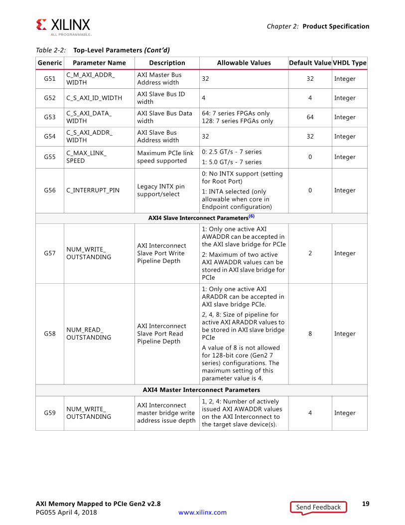
G51 C_M_AXI_ADDR_WIDTH
AXI Master Bus Address width 32 32 Integer
G52 C_S_AXI_ID_WIDTH AXI Slave Bus ID width 4 4 Integer
G53 C_S_AXI_DATA_WIDTH
AXI Slave Bus Data width
64: 7 series FPGAs only128: 7 series FPGAs only 64 Integer
G54 C_S_AXI_ADDR_WIDTH
AXI Slave Bus Address width 32 32 Integer
G55 C_MAX_LINK_SPEED
Maximum PCIe link speed supported
0: 2.5 GT/s - 7 series
1: 5.0 GT/s - 7 series 0 Integer
G56 C_INTERRUPT_PIN Legacy INTX pin support/select
0: No INTX support (setting for Root Port)
1: INTA selected (only allowable when core in Endpoint configuration)
0 Integer
AXI4 Slave Interconnect Parameters(6)
G57 NUM_WRITE_OUTSTANDING
AXI Interconnect Slave Port Write Pipeline Depth
1: Only one active AXI AWADDR can be accepted in the AXI slave bridge for PCIe
2: Maximum of two active AXI AWADDR values can be stored in AXI slave bridge for PCIe
2 Integer
G58 NUM_READ_OUTSTANDING
AXI Interconnect Slave Port Read Pipeline Depth
1: Only one active AXI ARADDR can be accepted in AXI slave bridge PCIe.
2, 4, 8: Size of pipeline for active AXI ARADDR values to be stored in AXI slave bridge PCIe
A value of 8 is not allowed for 128-bit core (Gen2 7 series) configurations. The maximum setting of this parameter value is 4.
8 Integer
AXI4 Master Interconnect Parameters
G59 NUM_WRITE_OUTSTANDING
AXI Interconnect master bridge write address issue depth
1, 2, 4: Number of actively issued AXI AWADDR values on the AXI Interconnect to the target slave device(s).
4 Integer
Table 2-2: Top-Level Parameters (Cont’d)
Generic Parameter Name Description Allowable Values Default Value VHDL Type
Send Feedback
AXI Memory Mapped to PCIe Gen2 v2.8 20PG055 April 4, 2018 www.xilinx.com
Chapter 2: Product Specification
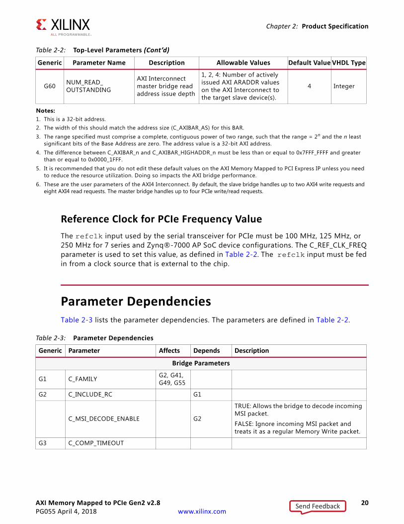
Reference Clock for PCIe Frequency ValueThe refclk input used by the serial transceiver for PCIe must be 100 MHz, 125 MHz, or 250 MHz for 7 series and Zynq®-7000 AP SoC device configurations. The C_REF_CLK_FREQ parameter is used to set this value, as defined in Table 2-2. The refclk input must be fed in from a clock source that is external to the chip.
Parameter DependenciesTable 2-3 lists the parameter dependencies. The parameters are defined in Table 2-2.
G60 NUM_READ_OUTSTANDING
AXI Interconnect master bridge read address issue depth
1, 2, 4: Number of actively issued AXI ARADDR values on the AXI Interconnect to the target slave device(s).
4 Integer
Notes: 1. This is a 32-bit address.2. The width of this should match the address size (C_AXIBAR_AS) for this BAR.3. The range specified must comprise a complete, contiguous power of two range, such that the range = 2n and the n least
significant bits of the Base Address are zero. The address value is a 32-bit AXI address.4. The difference between C_AXIBAR_n and C_AXIBAR_HIGHADDR_n must be less than or equal to 0x7FFF_FFFF and greater
than or equal to 0x0000_1FFF.5. It is recommended that you do not edit these default values on the AXI Memory Mapped to PCI Express IP unless you need
to reduce the resource utilization. Doing so impacts the AXI bridge performance.6. These are the user parameters of the AXI4 Interconnect. By default, the slave bridge handles up to two AXI4 write requests and
eight AXI4 read requests. The master bridge handles up to four PCIe write/read requests.
Table 2-2: Top-Level Parameters (Cont’d)
Generic Parameter Name Description Allowable Values Default Value VHDL Type
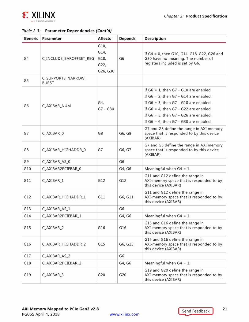
Table 2-3: Parameter Dependencies
Generic Parameter Affects Depends Description
Bridge Parameters
G1 C_FAMILY G2, G41, G49, G55
G2 C_INCLUDE_RC G1
C_MSI_DECODE_ENABLE G2
TRUE: Allows the bridge to decode incoming MSI packet.
FALSE: Ignore incoming MSI packet and treats it as a regular Memory Write packet.
G3 C_COMP_TIMEOUT
Send Feedback
AXI Memory Mapped to PCIe Gen2 v2.8 21PG055 April 4, 2018 www.xilinx.com
Chapter 2: Product Specification
G4 C_INCLUDE_BAROFFSET_REG
G10,
G14,
G18,
G22,
G26, G30
G6If G4 = 0, then G10, G14, G18, G22, G26 and G30 have no meaning. The number of registers included is set by G6.
G5 C_SUPPORTS_NARROW_BURST
G6 C_AXIBAR_NUMG4,
G7 - G30
If G6 = 1, then G7 - G10 are enabled.
If G6 = 2, then G7 - G14 are enabled.
If G6 = 3, then G7 - G18 are enabled.
If G6 = 4, then G7 - G22 are enabled.
If G6 = 5, then G7 - G26 are enabled.
If G6 = 6, then G7 - G30 are enabled.
G7 C_AXIBAR_0 G8 G6, G8G7 and G8 define the range in AXI memory space that is responded to by this device (AXIBAR)
G8 C_AXIBAR_HIGHADDR_0 G7 G6, G7G7 and G8 define the range in AXI memory space that is responded to by this device (AXIBAR)
G9 C_AXIBAR_AS_0 G6
G10 C_AXIBAR2PCIEBAR_0 G4, G6 Meaningful when G4 = 1.
G11 C_AXIBAR_1 G12 G12G11 and G12 define the range in AXI-memory space that is responded to by this device (AXIBAR)
G12 C_AXIBAR_HIGHADDR_1 G11 G6, G11G11 and G12 define the range in AXI-memory space that is responded to by this device (AXIBAR)
G13 C_AXIBAR_AS_1 G6
G14 C_AXIBAR2PCIEBAR_1 G4, G6 Meaningful when G4 = 1.
G15 C_AXIBAR_2 G16 G16G15 and G16 define the range in AXI-memory space that is responded to by this device (AXIBAR)
G16 C_AXIBAR_HIGHADDR_2 G15 G6, G15G15 and G16 define the range in AXI-memory space that is responded to by this device (AXIBAR)
G17 C_AXIBAR_AS_2 G6
G18 C_AXIBAR2PCIEBAR_2 G4, G6 Meaningful when G4 = 1.
G19 C_AXIBAR_3 G20 G20G19 and G20 define the range in AXI-memory space that is responded to by this device (AXIBAR)
Table 2-3: Parameter Dependencies (Cont’d)
Generic Parameter Affects Depends Description
Send Feedback
AXI Memory Mapped to PCIe Gen2 v2.8 22PG055 April 4, 2018 www.xilinx.com
Chapter 2: Product Specification
G20 C_AXIBAR_HIGHADDR_3 G19 G6, G19G19 and G20 define the range in AXI-memory space that is responded to by this device (AXIBAR)
G21 C_AXIBAR_AS_3 G6
G22 C_AXIBAR2PCIEBAR_3 G4, G6 Meaningful when G4 = 1.
G23 C_AXIBAR_4 G24 G24G23 and G24 define the range in AXI-memory space that is responded to by this device (AXIBAR)
G24 C_AXIBAR_HIGHADDR_4 G23 G6, G23G23 and G24 define the range in AXI-memory space that is responded to by this device (AXIBAR)
G25 C_AXIBAR_AS_4 G6
G26 C_AXIBAR2PCIEBAR_4 G4, G6 Meaningful if G4 = 1.
G27 C_AXIBAR_5 G28 G28G27 and G28 define the range in AXI-memory space that is responded to by this device (AXIBAR)
G28 C_AXIBAR_HIGHADDR_5 G27 G6, G27G27 and G28 define the range in AXI-memory space that is responded to by this device (AXIBAR)
G29 C_AXIBAR_AS_5 G6
G30 C_AXIBAR2PCIEBAR_5 G4, G6 Meaningful if G4 = 1.
G31 C_PCIEBAR_NUM G33-G38
If G31 = 1, then G32, G33 are enabled.
If G31 = 2, then G32 - G36 are enabled.
If G31 = 3, then G32 - G38 are enabled
G32 C_PCIEBAR_AS
G33 C_PCIEBAR_LEN_0 G34 G31
G34 C_PCIEBAR2AXIBAR_0 G31, G33 Only the high-order bits above the length defined by G33 are meaningful.
G35 C_PCIEBAR_LEN_1 G36 G31
G36 C_PCIEBAR2AXIBAR_1 G31, G35 Only the high-order bits above the length defined by G35 are meaningful.
G37 C_PCIEBAR_LEN_2 G38 G31
G38 C_PCIEBAR2AXIBAR_2 G31, G37 Only the high-order bits above the length defined by G37 are meaningful.
Table 2-3: Parameter Dependencies (Cont’d)
Generic Parameter Affects Depends Description
Send Feedback
AXI Memory Mapped to PCIe Gen2 v2.8 23PG055 April 4, 2018 www.xilinx.com
Chapter 2: Product Specification
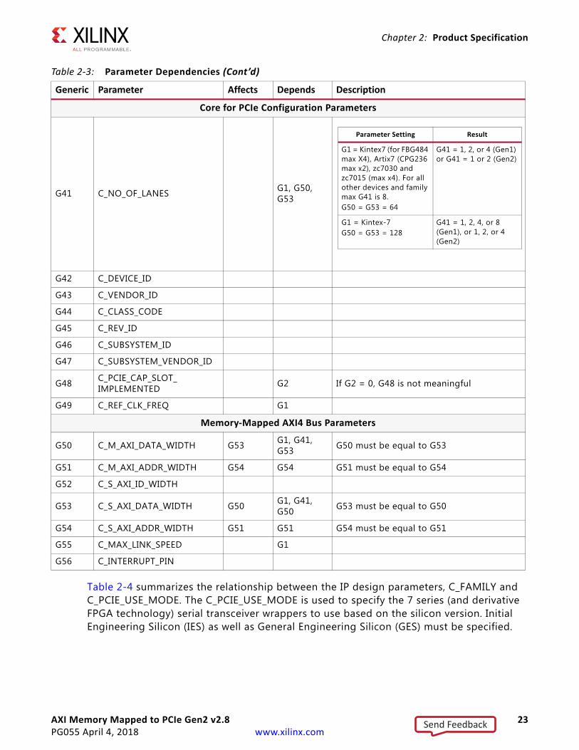
Table 2-4 summarizes the relationship between the IP design parameters, C_FAMILY and C_PCIE_USE_MODE. The C_PCIE_USE_MODE is used to specify the 7 series (and derivative FPGA technology) serial transceiver wrappers to use based on the silicon version. Initial Engineering Silicon (IES) as well as General Engineering Silicon (GES) must be specified.
Core for PCIe Configuration Parameters
G41 C_NO_OF_LANES G1, G50, G53
G42 C_DEVICE_ID
G43 C_VENDOR_ID
G44 C_CLASS_CODE
G45 C_REV_ID
G46 C_SUBSYSTEM_ID
G47 C_SUBSYSTEM_VENDOR_ID
G48 C_PCIE_CAP_SLOT_IMPLEMENTED G2 If G2 = 0, G48 is not meaningful
G49 C_REF_CLK_FREQ G1
Memory-Mapped AXI4 Bus Parameters
G50 C_M_AXI_DATA_WIDTH G53 G1, G41, G53 G50 must be equal to G53
G51 C_M_AXI_ADDR_WIDTH G54 G54 G51 must be equal to G54
G52 C_S_AXI_ID_WIDTH
G53 C_S_AXI_DATA_WIDTH G50 G1, G41, G50 G53 must be equal to G50
G54 C_S_AXI_ADDR_WIDTH G51 G51 G54 must be equal to G51
G55 C_MAX_LINK_SPEED G1
G56 C_INTERRUPT_PIN
Table 2-3: Parameter Dependencies (Cont’d)
Generic Parameter Affects Depends Description
Parameter Setting Result
G1 = Kintex7 (for FBG484 max X4), Artix7 (CPG236 max x2), zc7030 and zc7015 (max x4). For all other devices and family max G41 is 8.G50 = G53 = 64
G41 = 1, 2, or 4 (Gen1) or G41 = 1 or 2 (Gen2)
G1 = Kintex-7 G50 = G53 = 128
G41 = 1, 2, 4, or 8 (Gen1), or 1, 2, or 4 (Gen2)
Send Feedback
AXI Memory Mapped to PCIe Gen2 v2.8 24PG055 April 4, 2018 www.xilinx.com
Chapter 2: Product Specification
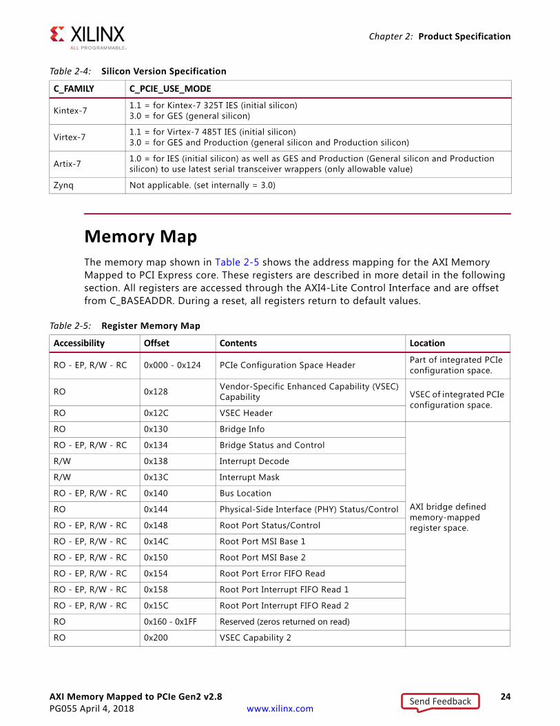
Memory MapThe memory map shown in Table 2-5 shows the address mapping for the AXI Memory Mapped to PCI Express core. These registers are described in more detail in the following section. All registers are accessed through the AXI4-Lite Control Interface and are offset from C_BASEADDR. During a reset, all registers return to default values.
Table 2-4: Silicon Version Specification
C_FAMILY C_PCIE_USE_MODE
Kintex-7 1.1 = for Kintex-7 325T IES (initial silicon)3.0 = for GES (general silicon)
Virtex-7 1.1 = for Virtex-7 485T IES (initial silicon)3.0 = for GES and Production (general silicon and Production silicon)
Artix-7 1.0 = for IES (initial silicon) as well as GES and Production (General silicon and Production silicon) to use latest serial transceiver wrappers (only allowable value)
Zynq Not applicable. (set internally = 3.0)
Table 2-5: Register Memory Map
Accessibility Offset Contents Location
RO - EP, R/W - RC 0x000 - 0x124 PCIe Configuration Space Header Part of integrated PCIe configuration space.
RO 0x128 Vendor-Specific Enhanced Capability (VSEC) Capability VSEC of integrated PCIe
configuration space.RO 0x12C VSEC Header
RO 0x130 Bridge Info
AXI bridge defined memory-mapped register space.
RO - EP, R/W - RC 0x134 Bridge Status and Control
R/W 0x138 Interrupt Decode
R/W 0x13C Interrupt Mask
RO - EP, R/W - RC 0x140 Bus Location
RO 0x144 Physical-Side Interface (PHY) Status/Control
RO - EP, R/W - RC 0x148 Root Port Status/Control
RO - EP, R/W - RC 0x14C Root Port MSI Base 1
RO - EP, R/W - RC 0x150 Root Port MSI Base 2
RO - EP, R/W - RC 0x154 Root Port Error FIFO Read
RO - EP, R/W - RC 0x158 Root Port Interrupt FIFO Read 1
RO - EP, R/W - RC 0x15C Root Port Interrupt FIFO Read 2
RO 0x160 - 0x1FF Reserved (zeros returned on read)
RO 0x200 VSEC Capability 2
Send Feedback
AXI Memory Mapped to PCIe Gen2 v2.8 25PG055 April 4, 2018 www.xilinx.com
Chapter 2: Product Specification
PCIe Configuration Space HeaderThe PCIe Configuration Space Header is a memory aperture for accessing the core for PCIe configuration space. For 7 series devices, this area is read-only when configured as an Endpoint. Writes are permitted for some registers when a 7 series device is configured as a Root Port. Special access modes can be enabled using the PHY Status/Control register. All reserved or undefined memory-mapped addresses must return zero and writes have no effect.
VSEC Capability Register (Offset 0x128)The VSEC Capability register (described in Table 2-6) allows the memory space of the core to appear as though it is a part of the underlying core configuration space. The VSEC is inserted immediately following the last enhanced capability structure in the underlying block. VSEC is defined in §7.18 of the PCI Express Base Specification, v1.1 (§7.19 of v2.0) [Ref 8].
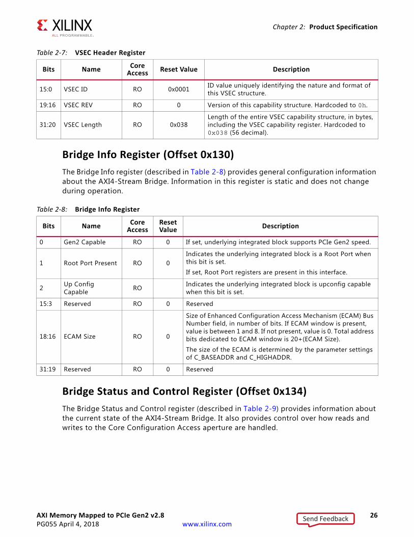
VSEC Header Register (Offset 0x12C)The VSEC Header register (described in Table 2-7) provides a unique (within a given vendor) identifier for the layout and contents of the VSEC structure, as well as its revision and length.
VSEC Header register is part of the PCI Express Hard Block which contains Loopback Control registers. For more information about Loopback Control Registers, see the “Xilinx Defined Vendor Specific Capability” section in the 7 Series FPGAs Integrated Block for PCI Express Product Guide (PG054) [Ref 2].
RO 0x204 VSEC Header 2
R/W 0x208 - 0x234 AXI Base Address Translation Configuration Registers
AXI bridge defined memory-mapped space.
RO 0x238 - 0xFFF Reserved (zeros returned on read)
Table 2-5: Register Memory Map (Cont’d)
Accessibility Offset Contents Location
Table 2-6: VSEC Capability Register
Bits Name Core Access Reset Value Description
15:0 VSEC Capability ID RO 0x000BPCI-SIG® defined ID identifying this enhanced capability as a vendor-specific capability. Hardcoded to 0x000B.
19:16 Capability Version RO 0x1 Version of this capability structure. Hardcoded to 0x1.
31:20 Next Capability Offset RO 0x200 Offset to next capability. Hardcoded to 0x0200.
Send Feedback
AXI Memory Mapped to PCIe Gen2 v2.8 26PG055 April 4, 2018 www.xilinx.com
Chapter 2: Product Specification
Bridge Info Register (Offset 0x130)The Bridge Info register (described in Table 2-8) provides general configuration information about the AXI4-Stream Bridge. Information in this register is static and does not change during operation.
Bridge Status and Control Register (Offset 0x134) The Bridge Status and Control register (described in Table 2-9) provides information about the current state of the AXI4-Stream Bridge. It also provides control over how reads and writes to the Core Configuration Access aperture are handled.
Table 2-7: VSEC Header Register
Bits Name Core Access Reset Value Description
15:0 VSEC ID RO 0x0001 ID value uniquely identifying the nature and format of this VSEC structure.
19:16 VSEC REV RO 0 Version of this capability structure. Hardcoded to 0h.
31:20 VSEC Length RO 0x038Length of the entire VSEC capability structure, in bytes, including the VSEC capability register. Hardcoded to 0x038 (56 decimal).
Table 2-8: Bridge Info Register
Bits Name Core Access
Reset Value Description
0 Gen2 Capable RO 0 If set, underlying integrated block supports PCIe Gen2 speed.
1 Root Port Present RO 0Indicates the underlying integrated block is a Root Port when this bit is set.
If set, Root Port registers are present in this interface.
2 Up Config Capable RO Indicates the underlying integrated block is upconfig capable
when this bit is set.
15:3 Reserved RO 0 Reserved
18:16 ECAM Size RO 0
Size of Enhanced Configuration Access Mechanism (ECAM) Bus Number field, in number of bits. If ECAM window is present, value is between 1 and 8. If not present, value is 0. Total address bits dedicated to ECAM window is 20+(ECAM Size).
The size of the ECAM is determined by the parameter settings of C_BASEADDR and C_HIGHADDR.
31:19 Reserved RO 0 Reserved
Send Feedback
AXI Memory Mapped to PCIe Gen2 v2.8 27PG055 April 4, 2018 www.xilinx.com
Chapter 2: Product Specification
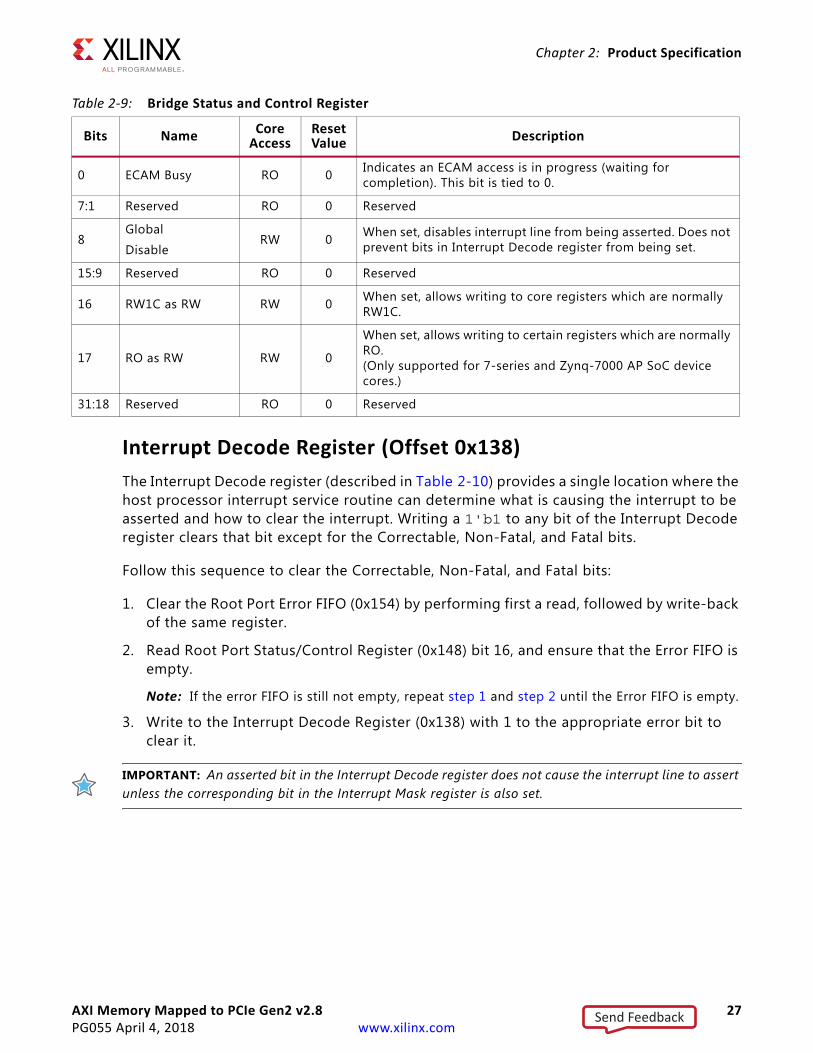
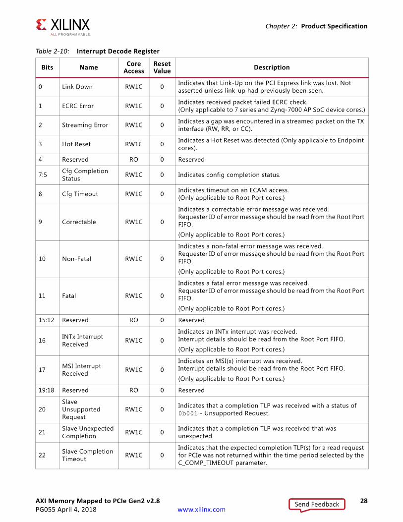
Interrupt Decode Register (Offset 0x138)The Interrupt Decode register (described in Table 2-10) provides a single location where the host processor interrupt service routine can determine what is causing the interrupt to be asserted and how to clear the interrupt. Writing a 1'b1 to any bit of the Interrupt Decode register clears that bit except for the Correctable, Non-Fatal, and Fatal bits.
Follow this sequence to clear the Correctable, Non-Fatal, and Fatal bits:
1. Clear the Root Port Error FIFO (0x154) by performing first a read, followed by write-back of the same register.
2. Read Root Port Status/Control Register (0x148) bit 16, and ensure that the Error FIFO is empty.
Note: If the error FIFO is still not empty, repeat step 1 and step 2 until the Error FIFO is empty.
3. Write to the Interrupt Decode Register (0x138) with 1 to the appropriate error bit to clear it.
IMPORTANT: An asserted bit in the Interrupt Decode register does not cause the interrupt line to assert unless the corresponding bit in the Interrupt Mask register is also set.
Table 2-9: Bridge Status and Control Register
Bits Name Core Access
Reset Value Description
0 ECAM Busy RO 0 Indicates an ECAM access is in progress (waiting for completion). This bit is tied to 0.
7:1 Reserved RO 0 Reserved
8Global
DisableRW 0 When set, disables interrupt line from being asserted. Does not
prevent bits in Interrupt Decode register from being set.
15:9 Reserved RO 0 Reserved
16 RW1C as RW RW 0 When set, allows writing to core registers which are normally RW1C.
17 RO as RW RW 0
When set, allows writing to certain registers which are normally RO. (Only supported for 7-series and Zynq-7000 AP SoC device cores.)
31:18 Reserved RO 0 Reserved
Send Feedback
AXI Memory Mapped to PCIe Gen2 v2.8 28PG055 April 4, 2018 www.xilinx.com
Chapter 2: Product Specification
Table 2-10: Interrupt Decode Register
Bits Name Core Access
Reset Value Description
0 Link Down RW1C 0 Indicates that Link-Up on the PCI Express link was lost. Not asserted unless link-up had previously been seen.
1 ECRC Error RW1C 0 Indicates received packet failed ECRC check. (Only applicable to 7 series and Zynq-7000 AP SoC device cores.)
2 Streaming Error RW1C 0 Indicates a gap was encountered in a streamed packet on the TX interface (RW, RR, or CC).
3 Hot Reset RW1C 0 Indicates a Hot Reset was detected (Only applicable to Endpoint cores).
4 Reserved RO 0 Reserved
7:5 Cfg Completion Status RW1C 0 Indicates config completion status.
8 Cfg Timeout RW1C 0 Indicates timeout on an ECAM access. (Only applicable to Root Port cores.)
9 Correctable RW1C 0
Indicates a correctable error message was received.Requester ID of error message should be read from the Root Port FIFO.
(Only applicable to Root Port cores.)
10 Non-Fatal RW1C 0
Indicates a non-fatal error message was received. Requester ID of error message should be read from the Root Port FIFO.
(Only applicable to Root Port cores.)
11 Fatal RW1C 0
Indicates a fatal error message was received. Requester ID of error message should be read from the Root Port FIFO.
(Only applicable to Root Port cores.)
15:12 Reserved RO 0 Reserved
16 INTx Interrupt Received RW1C 0
Indicates an INTx interrupt was received.Interrupt details should be read from the Root Port FIFO.
(Only applicable to Root Port cores.)
17 MSI Interrupt Received RW1C 0
Indicates an MSI(x) interrupt was received.Interrupt details should be read from the Root Port FIFO.
(Only applicable to Root Port cores.)
19:18 Reserved RO 0 Reserved
20Slave Unsupported Request
RW1C 0 Indicates that a completion TLP was received with a status of 0b001 - Unsupported Request.
21 Slave Unexpected Completion RW1C 0 Indicates that a completion TLP was received that was
unexpected.
22 Slave Completion Timeout RW1C 0
Indicates that the expected completion TLP(s) for a read request for PCIe was not returned within the time period selected by the C_COMP_TIMEOUT parameter.
Send Feedback
AXI Memory Mapped to PCIe Gen2 v2.8 29PG055 April 4, 2018 www.xilinx.com
Chapter 2: Product Specification
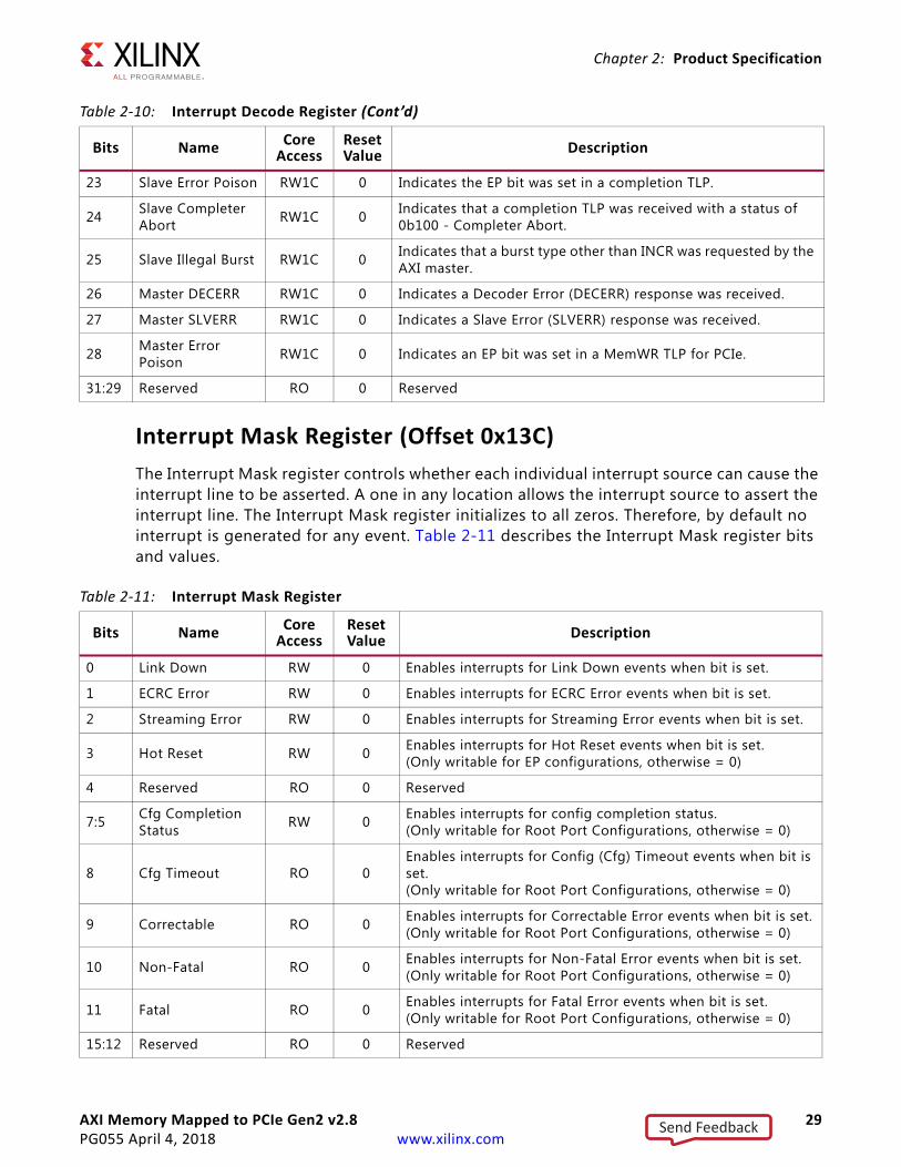
Interrupt Mask Register (Offset 0x13C)The Interrupt Mask register controls whether each individual interrupt source can cause the interrupt line to be asserted. A one in any location allows the interrupt source to assert the interrupt line. The Interrupt Mask register initializes to all zeros. Therefore, by default no interrupt is generated for any event. Table 2-11 describes the Interrupt Mask register bits and values.
23 Slave Error Poison RW1C 0 Indicates the EP bit was set in a completion TLP.
24 Slave Completer Abort RW1C 0 Indicates that a completion TLP was received with a status of
0b100 - Completer Abort.
25 Slave Illegal Burst RW1C 0 Indicates that a burst type other than INCR was requested by the AXI master.
26 Master DECERR RW1C 0 Indicates a Decoder Error (DECERR) response was received.
27 Master SLVERR RW1C 0 Indicates a Slave Error (SLVERR) response was received.
28 Master Error Poison RW1C 0 Indicates an EP bit was set in a MemWR TLP for PCIe.
31:29 Reserved RO 0 Reserved
Table 2-10: Interrupt Decode Register (Cont’d)
Bits Name Core Access
Reset Value Description
Table 2-11: Interrupt Mask Register
Bits Name Core Access
Reset Value Description
0 Link Down RW 0 Enables interrupts for Link Down events when bit is set.
1 ECRC Error RW 0 Enables interrupts for ECRC Error events when bit is set.
2 Streaming Error RW 0 Enables interrupts for Streaming Error events when bit is set.
3 Hot Reset RW 0 Enables interrupts for Hot Reset events when bit is set.(Only writable for EP configurations, otherwise = 0)
4 Reserved RO 0 Reserved
7:5 Cfg Completion Status RW 0 Enables interrupts for config completion status.
(Only writable for Root Port Configurations, otherwise = 0)
8 Cfg Timeout RO 0Enables interrupts for Config (Cfg) Timeout events when bit is set.(Only writable for Root Port Configurations, otherwise = 0)
9 Correctable RO 0 Enables interrupts for Correctable Error events when bit is set.(Only writable for Root Port Configurations, otherwise = 0)
10 Non-Fatal RO 0 Enables interrupts for Non-Fatal Error events when bit is set.(Only writable for Root Port Configurations, otherwise = 0)
11 Fatal RO 0 Enables interrupts for Fatal Error events when bit is set.(Only writable for Root Port Configurations, otherwise = 0)
15:12 Reserved RO 0 Reserved
Send Feedback

AXI Memory Mapped to PCIe Gen2 v2.8 30PG055 April 4, 2018 www.xilinx.com
Chapter 2: Product Specification
Bus Location Register (Offset 0x140)The Bus Location register reports the Bus, Device, and Function number, and the Port number for the PCIe port (Table 2-12).
16 INTx Interrupt Received RO 0 Enables interrupts for INTx Interrupt events when bit is set.
(Only writable for Root Port Configurations, otherwise =0)
17 MSI Interrupt Received RO 0 Enables interrupts for MSI Interrupt events when bit is set.
(Only writable for Root Port Configurations, otherwise =0)
19:18 Reserved RO 0 Reserved
20Slave Unsupported Request
RW 0 Enables the Slave Unsupported Request interrupt when bit is set.
21 Slave Unexpected Completion RW 0 Enables the Slave Unexpected Completion interrupt when bit is
set.
22 Slave Completion Timeout RW 0 Enables the Slave Completion Timeout interrupt when bit is set.
23 Slave Error Poison RW 0 Enables the Slave Error Poison interrupt when bit is set.
24 Slave Completer Abort RW 0 Enables the Slave Completer Abort interrupt when bit is set.
25 Slave Illegal Burst RW 0 Enables the Slave Illegal Burst interrupt when bit is set.
26 Master DECERR RW 0 Enables the Master DECERR interrupt when bit is set.
27 Master SLVERR RW 0 Enables the Master SLVERR interrupt when bit is set.
28 Master Error Poison RW 0 Enables the Master Error Poison interrupt when bit is set.
31:29 Reserved RO 0 Reserved
Table 2-11: Interrupt Mask Register (Cont’d)
Bits Name Core Access
Reset Value Description
Table 2-12: Bus Location Register
Bits Name Core Access
Reset Value Description
2:0 Function Number RO 0 Function number of the port for PCIe. Hard-wired to 0.
7:3 Device Number RO 0 Device number of port for PCIe. For Endpoint, this register is RO and is set by the Root Port.
15:8 Bus Number RO 0 Bus number of port for PCIe. For Endpoint, this register is RO and is set by the external Root Port.
23:16 Port Number RW 0Sets the Port number field of the Link Capabilities register. EP: Read Only on all devices except for Spartan-6 FPGA.
RP: Read and writeable.
31:24 Reserved RO 0 Reserved
Send Feedback
AXI Memory Mapped to PCIe Gen2 v2.8 31PG055 April 4, 2018 www.xilinx.com
Chapter 2: Product Specification
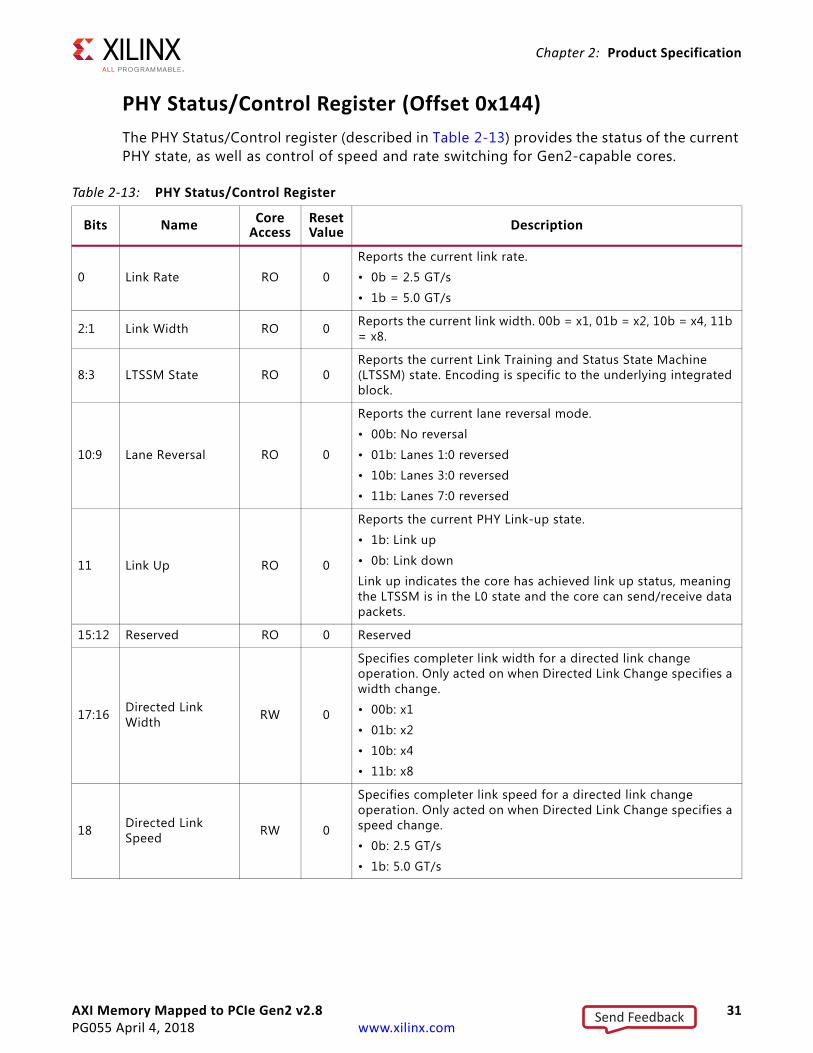
PHY Status/Control Register (Offset 0x144)The PHY Status/Control register (described in Table 2-13) provides the status of the current PHY state, as well as control of speed and rate switching for Gen2-capable cores.
Table 2-13: PHY Status/Control Register
Bits Name Core Access
Reset Value Description
0 Link Rate RO 0
Reports the current link rate.
• 0b = 2.5 GT/s
• 1b = 5.0 GT/s
2:1 Link Width RO 0 Reports the current link width. 00b = x1, 01b = x2, 10b = x4, 11b = x8.
8:3 LTSSM State RO 0Reports the current Link Training and Status State Machine (LTSSM) state. Encoding is specific to the underlying integrated block.
10:9 Lane Reversal RO 0
Reports the current lane reversal mode.
• 00b: No reversal
• 01b: Lanes 1:0 reversed
• 10b: Lanes 3:0 reversed
• 11b: Lanes 7:0 reversed
11 Link Up RO 0
Reports the current PHY Link-up state.
• 1b: Link up
• 0b: Link down
Link up indicates the core has achieved link up status, meaning the LTSSM is in the L0 state and the core can send/receive data packets.
15:12 Reserved RO 0 Reserved
17:16 Directed Link Width RW 0
Specifies completer link width for a directed link change operation. Only acted on when Directed Link Change specifies a width change.
• 00b: x1
• 01b: x2
• 10b: x4
• 11b: x8
18 Directed Link Speed RW 0
Specifies completer link speed for a directed link change operation. Only acted on when Directed Link Change specifies a speed change.
• 0b: 2.5 GT/s
• 1b: 5.0 GT/s
Send Feedback

AXI Memory Mapped to PCIe Gen2 v2.8 32PG055 April 4, 2018 www.xilinx.com
Chapter 2: Product Specification
Root Port Status/Control Register (Offset 0x148)The Root Port Status/Control register provides access to Root Port specific status and control. This register is only implemented for Root Port cores. For non-Root Port cores, reads return 0 and writes are ignored (described in Table 2-14).
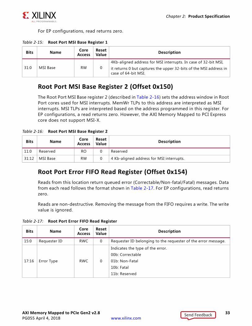
Root Port MSI Base Register 1 (Offset 0x14C)The Root Port MSI Base register contains the upper 32-bits of the 64-bit MSI address (described in Table 2-15).
19 Directed Link Autonomous RW 0
Specifies link reliability or autonomous for directed link change operation.
• 0b: Link reliability
• 1b: Autonomous
21:20 Directed Link Change RW 0
Directs LTSSM to initiate a link width and/or speed change.
• 00b: No change
• 01b: Force link width
• 10b: Force link speed
• 11b: Force link width and speed
31:22 Reserved RO 0 Reserved
Table 2-13: PHY Status/Control Register (Cont’d)
Bits Name Core Access
Reset Value Description
Table 2-14: Root Port Status/Control Register
Bits Name Core Access
Reset Value Description
0 Bridge Enable RW 0
When set, allows the reads and writes to the AXIBARs to be presented on the PCIe bus. Root Port software needs to write 1 to this bit when enumeration is done. AXI Enhanced PCIe Bridge clears this location when link up to link down transition occurs. Default is set to 0.
15:1 Reserved RO 0 Reserved.
16 Error FIFO Not Empty RO 0 Indicates that the Root Port Error FIFO has data to read.
17 Error FIFO Overflow RW1C 0 Indicates that the Root Port Error FIFO overflowed and an error
message was dropped. Writing a 1 clears the overflow status.
18 Interrupt FIFO Not Empty RO 0 Indicates that the Root Port Interrupt FIFO has data to read.
19 Interrupt FIFO Overflow RW1C 0
Indicates that the Root Port Interrupt FIFO overflowed and an interrupt message was dropped. Writing a 1 clears the overflow status
31:20 Reserved RO 0 Reserved.
Send Feedback
AXI Memory Mapped to PCIe Gen2 v2.8 33PG055 April 4, 2018 www.xilinx.com
Chapter 2: Product Specification
For EP configurations, read returns zero.
Root Port MSI Base Register 2 (Offset 0x150)The Root Port MSI Base register 2 (described in Table 2-16) sets the address window in Root Port cores used for MSI interrupts. MemWr TLPs to this address are interpreted as MSI interrupts. MSI TLPs are interpreted based on the address programmed in this register. For EP configurations, a read returns zero. However, the AXI Memory Mapped to PCI Express core does not support MSI-X.
Root Port Error FIFO Read Register (Offset 0x154)Reads from this location return queued error (Correctable/Non-fatal/Fatal) messages. Data from each read follows the format shown in Table 2-17. For EP configurations, read returns zero.
Reads are non-destructive. Removing the message from the FIFO requires a write. The write value is ignored.
Table 2-15: Root Port MSI Base Register 1
Bits Name Core Access
Reset Value Description
31:0 MSI Base RW 04Kb-aligned address for MSI interrupts. In case of 32-bit MSI,
it returns 0 but captures the upper 32-bits of the MSI address in case of 64-bit MSI.
Table 2-16: Root Port MSI Base Register 2
Bits Name Core Access
Reset Value Description
11:0 Reserved RO 0 Reserved
31:12 MSI Base RW 0 4 Kb-aligned address for MSI interrupts.
Table 2-17: Root Port Error FIFO Read Register
Bits Name Core Access
Reset Value Description
15:0 Requester ID RWC 0 Requester ID belonging to the requester of the error message.
17:16 Error Type RWC 0
Indicates the type of the error.
00b: Correctable
01b: Non-Fatal
10b: Fatal
11b: Reserved
Send Feedback
AXI Memory Mapped to PCIe Gen2 v2.8 34PG055 April 4, 2018 www.xilinx.com
Chapter 2: Product Specification
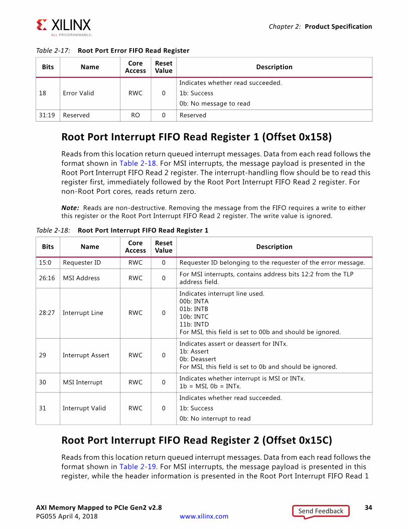
Root Port Interrupt FIFO Read Register 1 (Offset 0x158)Reads from this location return queued interrupt messages. Data from each read follows the format shown in Table 2-18. For MSI interrupts, the message payload is presented in the Root Port Interrupt FIFO Read 2 register. The interrupt-handling flow should be to read this register first, immediately followed by the Root Port Interrupt FIFO Read 2 register. For non-Root Port cores, reads return zero.
Note: Reads are non-destructive. Removing the message from the FIFO requires a write to either this register or the Root Port Interrupt FIFO Read 2 register. The write value is ignored.
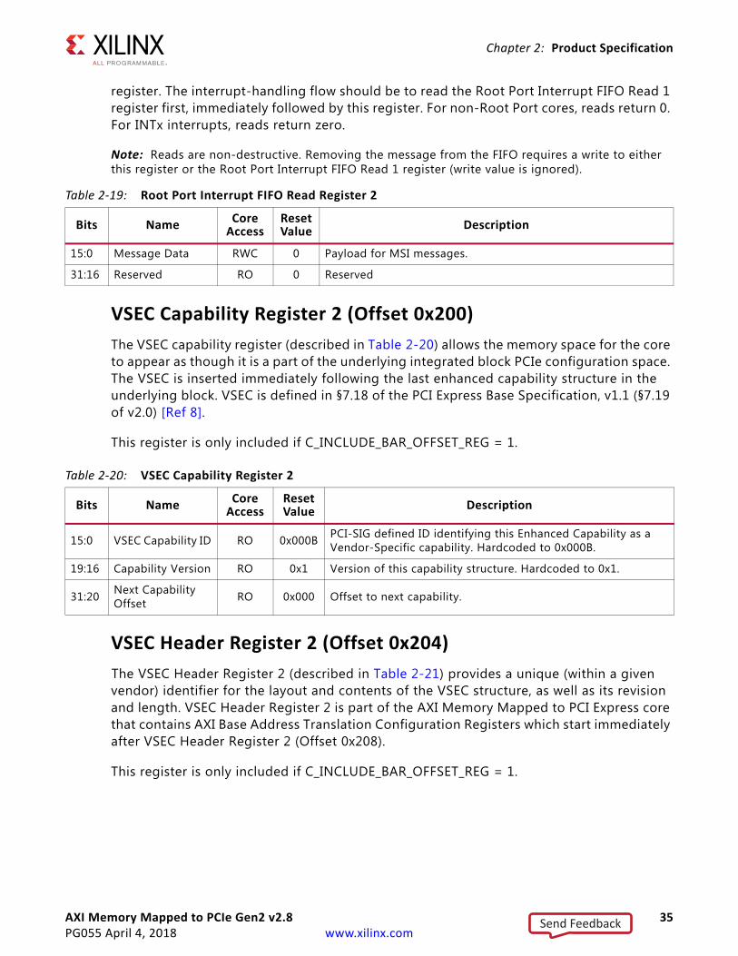
Root Port Interrupt FIFO Read Register 2 (Offset 0x15C)Reads from this location return queued interrupt messages. Data from each read follows the format shown in Table 2-19. For MSI interrupts, the message payload is presented in this register, while the header information is presented in the Root Port Interrupt FIFO Read 1
18 Error Valid RWC 0
Indicates whether read succeeded.
1b: Success
0b: No message to read
31:19 Reserved RO 0 Reserved
Table 2-17: Root Port Error FIFO Read Register
Bits Name Core Access
Reset Value Description
Table 2-18: Root Port Interrupt FIFO Read Register 1
Bits Name Core Access
Reset Value Description
15:0 Requester ID RWC 0 Requester ID belonging to the requester of the error message.
26:16 MSI Address RWC 0 For MSI interrupts, contains address bits 12:2 from the TLP address field.
28:27 Interrupt Line RWC 0
Indicates interrupt line used. 00b: INTA01b: INTB10b: INTC 11b: INTD For MSI, this field is set to 00b and should be ignored.
29 Interrupt Assert RWC 0
Indicates assert or deassert for INTx.1b: Assert0b: DeassertFor MSI, this field is set to 0b and should be ignored.
30 MSI Interrupt RWC 0 Indicates whether interrupt is MSI or INTx. 1b = MSI, 0b = INTx.
31 Interrupt Valid RWC 0
Indicates whether read succeeded.
1b: Success
0b: No interrupt to read
Send Feedback
AXI Memory Mapped to PCIe Gen2 v2.8 35PG055 April 4, 2018 www.xilinx.com
Chapter 2: Product Specification
register. The interrupt-handling flow should be to read the Root Port Interrupt FIFO Read 1 register first, immediately followed by this register. For non-Root Port cores, reads return 0. For INTx interrupts, reads return zero.
Note: Reads are non-destructive. Removing the message from the FIFO requires a write to either this register or the Root Port Interrupt FIFO Read 1 register (write value is ignored).
VSEC Capability Register 2 (Offset 0x200) The VSEC capability register (described in Table 2-20) allows the memory space for the core to appear as though it is a part of the underlying integrated block PCIe configuration space. The VSEC is inserted immediately following the last enhanced capability structure in the underlying block. VSEC is defined in §7.18 of the PCI Express Base Specification, v1.1 (§7.19 of v2.0) [Ref 8].
This register is only included if C_INCLUDE_BAR_OFFSET_REG = 1.
VSEC Header Register 2 (Offset 0x204)The VSEC Header Register 2 (described in Table 2-21) provides a unique (within a given vendor) identifier for the layout and contents of the VSEC structure, as well as its revision and length. VSEC Header Register 2 is part of the AXI Memory Mapped to PCI Express core that contains AXI Base Address Translation Configuration Registers which start immediately after VSEC Header Register 2 (Offset 0x208).
This register is only included if C_INCLUDE_BAR_OFFSET_REG = 1.
Table 2-19: Root Port Interrupt FIFO Read Register 2
Bits Name Core Access
Reset Value Description
15:0 Message Data RWC 0 Payload for MSI messages.
31:16 Reserved RO 0 Reserved
Table 2-20: VSEC Capability Register 2
Bits Name Core Access
Reset Value Description
15:0 VSEC Capability ID RO 0x000B PCI-SIG defined ID identifying this Enhanced Capability as a Vendor-Specific capability. Hardcoded to 0x000B.
19:16 Capability Version RO 0x1 Version of this capability structure. Hardcoded to 0x1.
31:20 Next Capability Offset RO 0x000 Offset to next capability.
Send Feedback

AXI Memory Mapped to PCIe Gen2 v2.8 36PG055 April 4, 2018 www.xilinx.com
Chapter 2: Product Specification
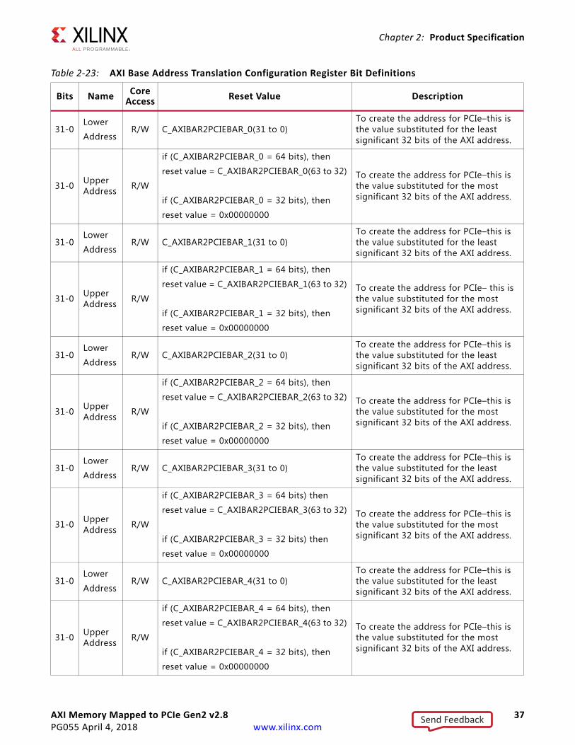
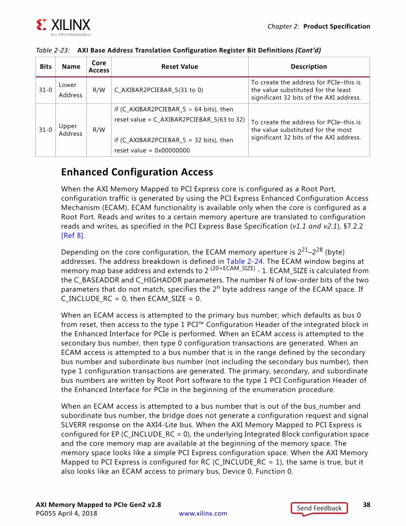
AXI Base Address Translation Configuration Registers (Offset 0x208 - 0x234)The AXI Base Address Translation Configuration Registers and their offsets are shown in Table 2-22 and the register bits are described in Table 2-23. This set of registers can be used in two configurations based on the top-level parameter C_AXIBAR_AS_n. When the BAR is set to a 32-bit address space, then the translation vector should be placed into the AXIBAR2PCIEBAR_nL register where n is the BAR number. When the BAR is set to a 64-bit address space, then the most significant 32 bits are written into the AXIBAR2PCIEBAR_nU and the least significant 32 bits are written into AXIBAR2PCIEBAR_nL. These registers are only included if C_INCLUDE_BAR_OFFSET_REG = 1.
Table 2-21: VSEC Header Register 2
Bits Name Core Access Reset Value Description
15:0 VSEC ID RO 0x0002 ID value uniquely identifying the nature and format of this VSEC structure.
19:16 VSEC REV RO 0x0 Version of this capability structure. Hardcoded to 0x0.
31:20 VSEC Length RO 0x038Length of the entire VSEC Capability structure, in bytes, including the VSEC Capability register. Hardcoded to 0x038 (56 decimal).
Table 2-22: AXI Base Address Translation Configuration Registers
Offset Bits Register Mnemonic
0x208 31-0 AXIBAR2PCIEBAR_0U
0x20C 31-0 AXIBAR2PCIEBAR_0L
0x210 31-0 AXIBAR2PCIEBAR_1U
0x214 31-0 AXIBAR2PCIEBAR_1L
0x218 31-0 AXIBAR2PCIEBAR_2U
0x21C 31-0 AXIBAR2PCIEBAR_2L
0x220 31-0 AXIBAR2PCIEBAR_3U
0x224 31-0 AXIBAR2PCIEBAR_3L
0x228 31-0 AXIBAR2PCIEBAR_4U
0x22C 31-0 AXIBAR2PCIEBAR_4L
0x230 31-0 AXIBAR2PCIEBAR_5U
0x234 31-0 AXIBAR2PCIEBAR_5L
Send Feedback
AXI Memory Mapped to PCIe Gen2 v2.8 37PG055 April 4, 2018 www.xilinx.com
Chapter 2: Product Specification
Table 2-23: AXI Base Address Translation Configuration Register Bit Definitions
Bits Name Core Access Reset Value Description
31-0Lower
AddressR/W C_AXIBAR2PCIEBAR_0(31 to 0)
To create the address for PCIe–this is the value substituted for the least significant 32 bits of the AXI address.
31-0 Upper Address R/W
if (C_AXIBAR2PCIEBAR_0 = 64 bits), then
reset value = C_AXIBAR2PCIEBAR_0(63 to 32)
if (C_AXIBAR2PCIEBAR_0 = 32 bits), then
reset value = 0x00000000
To create the address for PCIe–this is the value substituted for the most significant 32 bits of the AXI address.
31-0Lower
AddressR/W C_AXIBAR2PCIEBAR_1(31 to 0)
To create the address for PCIe–this is the value substituted for the least significant 32 bits of the AXI address.
31-0 Upper Address R/W
if (C_AXIBAR2PCIEBAR_1 = 64 bits), then
reset value = C_AXIBAR2PCIEBAR_1(63 to 32)
if (C_AXIBAR2PCIEBAR_1 = 32 bits), then
reset value = 0x00000000
To create the address for PCIe– this is the value substituted for the most significant 32 bits of the AXI address.
31-0Lower
AddressR/W C_AXIBAR2PCIEBAR_2(31 to 0)
To create the address for PCIe–this is the value substituted for the least significant 32 bits of the AXI address.
31-0 Upper Address R/W
if (C_AXIBAR2PCIEBAR_2 = 64 bits), then
reset value = C_AXIBAR2PCIEBAR_2(63 to 32)
if (C_AXIBAR2PCIEBAR_2 = 32 bits), then
reset value = 0x00000000
To create the address for PCIe–this is the value substituted for the most significant 32 bits of the AXI address.
31-0Lower
AddressR/W C_AXIBAR2PCIEBAR_3(31 to 0)
To create the address for PCIe–this is the value substituted for the least significant 32 bits of the AXI address.
31-0 Upper Address R/W
if (C_AXIBAR2PCIEBAR_3 = 64 bits) then
reset value = C_AXIBAR2PCIEBAR_3(63 to 32)
if (C_AXIBAR2PCIEBAR_3 = 32 bits) then
reset value = 0x00000000
To create the address for PCIe–this is the value substituted for the most significant 32 bits of the AXI address.
31-0Lower
AddressR/W C_AXIBAR2PCIEBAR_4(31 to 0)
To create the address for PCIe–this is the value substituted for the least significant 32 bits of the AXI address.
31-0 Upper Address R/W
if (C_AXIBAR2PCIEBAR_4 = 64 bits), then
reset value = C_AXIBAR2PCIEBAR_4(63 to 32)
if (C_AXIBAR2PCIEBAR_4 = 32 bits), then
reset value = 0x00000000
To create the address for PCIe–this is the value substituted for the most significant 32 bits of the AXI address.
Send Feedback
AXI Memory Mapped to PCIe Gen2 v2.8 38PG055 April 4, 2018 www.xilinx.com
Chapter 2: Product Specification
Enhanced Configuration AccessWhen the AXI Memory Mapped to PCI Express core is configured as a Root Port, configuration traffic is generated by using the PCI Express Enhanced Configuration Access Mechanism (ECAM). ECAM functionality is available only when the core is configured as a Root Port. Reads and writes to a certain memory aperture are translated to configuration reads and writes, as specified in the PCI Express Base Specification (v1.1 and v2.1), §7.2.2 [Ref 8].
Depending on the core configuration, the ECAM memory aperture is 221–228 (byte) addresses. The address breakdown is defined in Table 2-24. The ECAM window begins at memory map base address and extends to 2 (20+ECAM_SIZE) - 1. ECAM_SIZE is calculated from the C_BASEADDR and C_HIGHADDR parameters. The number N of low-order bits of the two parameters that do not match, specifies the 2n byte address range of the ECAM space. If C_INCLUDE_RC = 0, then ECAM_SIZE = 0.
When an ECAM access is attempted to the primary bus number, which defaults as bus 0 from reset, then access to the type 1 PCI™ Configuration Header of the integrated block in the Enhanced Interface for PCIe is performed. When an ECAM access is attempted to the secondary bus number, then type 0 configuration transactions are generated. When an ECAM access is attempted to a bus number that is in the range defined by the secondary bus number and subordinate bus number (not including the secondary bus number), then type 1 configuration transactions are generated. The primary, secondary, and subordinate bus numbers are written by Root Port software to the type 1 PCI Configuration Header of the Enhanced Interface for PCIe in the beginning of the enumeration procedure.
When an ECAM access is attempted to a bus number that is out of the bus_number and subordinate bus number, the bridge does not generate a configuration request and signal SLVERR response on the AXI4-Lite bus. When the AXI Memory Mapped to PCI Express is configured for EP (C_INCLUDE_RC = 0), the underlying Integrated Block configuration space and the core memory map are available at the beginning of the memory space. The memory space looks like a simple PCI Express configuration space. When the AXI Memory Mapped to PCI Express is configured for RC (C_INCLUDE_RC = 1), the same is true, but it also looks like an ECAM access to primary bus, Device 0, Function 0.
31-0Lower
AddressR/W C_AXIBAR2PCIEBAR_5(31 to 0)
To create the address for PCIe–this is the value substituted for the least significant 32 bits of the AXI address.
31-0 Upper Address R/W
if (C_AXIBAR2PCIEBAR_5 = 64 bits), then
reset value = C_AXIBAR2PCIEBAR_5(63 to 32)
if (C_AXIBAR2PCIEBAR_5 = 32 bits), then
reset value = 0x00000000
To create the address for PCIe–this is the value substituted for the most significant 32 bits of the AXI address.
Table 2-23: AXI Base Address Translation Configuration Register Bit Definitions (Cont’d)
Bits Name Core Access Reset Value Description
Send Feedback

AXI Memory Mapped to PCIe Gen2 v2.8 39PG055 April 4, 2018 www.xilinx.com
Chapter 2: Product Specification
When the AXI Memory Mapped to PCI Express core is configured as a Root Port, the reads and writes of the local ECAM are Bus 0. Because the FPGA only has a single Integrated Block for PCIe core, all local ECAM operations to Bus 0 return the ECAM data for Device 0, Function 0.
Configuration write accesses across the PCI Express bus are non-posted writes and block the AXI4-Lite interface while they are in progress. Because of this, system software is not able to service an interrupt if one were to occur. However, interrupts due to abnormal terminations of configuration transactions can generate interrupts. ECAM read transactions block subsequent Requester read TLPs until the configuration read completions packet is returned to allow unique identification of the completion packet.
Unsupported Memory SpaceAdvanced Error Reporting (AER) is not supported in the AXI Memory Mapped to PCI Express core. The AER register space is not accessible in the AXI Memory Mapped to PCI Express memory mapped space.
Table 2-24: ECAM Addressing
Bits Name Description
1:0 Byte Address Ignored for this implementation. The S_AXI_CTL_WSTRB[3:0] signals define byte enables for ECAM accesses.
7:2 Register Number Register within the configuration space to access.
11:8 Extended Register Number
Along with Register Number, allows access to PCI Express Extended Configuration Space.
14:12 Function Number Function Number to completer.
19:15 Device Number Device Number to completer.
(20+n-1):20 Bus NumberBus Number, 1 <= n <= 8. n is the number of bits available for Bus Number as derived from core parameters C_INCLUDE_RC, C_BASEADDR, and C_HIGHADDR.
Send Feedback
AXI Memory Mapped to PCIe Gen2 v2.8 40PG055 April 4, 2018 www.xilinx.com
Chapter 3
Designing with the CoreThis chapter includes guidelines and additional information to make designing with the core easier.
General Design GuidelinesThe Xilinx® Vivado® Design Suite has been optimized to provide a starting point for designing with the AXI Memory Mapped to PCI Express core.
ClockingFigure 3-1 shows the clocking diagram for the core. The main memory mapped AXI4 bus clock axi_aclk is driven by axi_aclk_out.
X-Ref Target - Figure 3-1
Figure 3-1: Clocking Diagram
AXI PCIe IP
axi_aclk
axi_ctl_aclk
axi_aclk_out
axi_ctl_aclk_out
mmcm_lock
refclkPCIe Reference Clock
X12325
Send Feedback
AXI Memory Mapped to PCIe Gen2 v2.8 41PG055 April 4, 2018 www.xilinx.com
Chapter 3: Designing with the Core
IMPORTANT: axi_aclk_out and axi_ctl_aclk_out are internally connected to axi_aclk and axi_ctl_aclk, respectively, and they do not need to be connected in the design.
The refclk input is used to generate the internal clocks used by the core and the output clocks. This clock must be provided at the reference clock frequency selected in the Vivado Integrated Design Environment (IDE) during IP generation.
The AXI4-Lite interconnect clock axi_ctl_aclk is driven by axi_ctl_aclk_out. The axi_ctl_aclk_out clock is rising edge aligned and an integer division of the axi_aclk_out clock.
The output clock frequency is 62.5 MHz for x1 gen1 64-bit AXI interface, and 125 MHz for the remaining configurations.
ResetsThe AXI Memory Mapped to PCI Express core is designed to be used with the Processing System Reset module for generation of the axi_areset input. When using the Vivado IP integrator to build a system, it is best to connect the perstn pin of the host connector for PCIe to the Aux_Reset_In port of the Processing System Reset module. The bridge does not use perstn directly. Also, the mmcm_lock output must be connected to the dcm_locked input of the Processing System Reset module to make sure that axi_aresetn is held active for 16 clocks after mmcm_lock becomes active. See Figure 3-2.
Note: Be sure to set the correct polarity on the aux_reset_in signal of the proc_sys_reset IP block. when PERSTN is active-Low, set the parameter as follows:
PARAMETER C_AUX_RESET_HIGH = 0
Send Feedback
AXI Memory Mapped to PCIe Gen2 v2.8 42PG055 April 4, 2018 www.xilinx.com
Chapter 3: Designing with the Core
Shared LogicThis new feature allows you to share common blocks across multiple instantiations. It minimizes the amount of required HDL modifications. You can use your own system-level clocking or reset circuit. You can modify some of these blocks due to system requirements (for example, swapping a BUFG for a BUFH). You can instantiate multiple cores and share 'common/shared logic' from one core among all instantiated cores. This is applicable for both Endpoint mode and Root Port mode.
In the Vivado Design Suite, the shared logic options are available in the Shared Logic page when customizing the core.
There are four types of logic sharing:
• Shared Clocking
• Shared GT_COMMON
• Shared GT_COMMON and Clocking
• Internal Shared GT_COMMON and Clocking
X-Ref Target - Figure 3-2
Figure 3-2: System Reset Connection
AXIPCIe IP
mmcm_lock
proc_sys_resetIP
PERSTn
DCM_LOCKED
Aux_Reset_In
Interconnect_aresetn AXI4 ARESETn
axi_aresetn
X12326
Send Feedback
AXI Memory Mapped to PCIe Gen2 v2.8 43PG055 April 4, 2018 www.xilinx.com
Chapter 3: Designing with the Core
Shared ClockingTo use the share clocking feature, select Include Shared Logic (Clocking) in example design option in the Shared Logic tab (Figure 3-3).
When this feature is selected, the mixed-mode clock manager (MMCM) instance is removed from the pipe wrappers and is moved into the support wrapper of the example design. It also brings out additional ports to the top level to enable sharing of the clocks.
You also have the option to modify and use the unused outputs of the MMCM.
The MMCM generates the following clocks for PCIe solution wrapper:
• clk_125mhz: 125 MHz clock.
• clk_250mhz: 250 MHz clock.
• userclk: 62.5 MHz/125 MHz/250 MHz clock, depending on selected PCIe core lane width, link speed, and AXI interface width.
• userclk2: 250 MHz/500 MHz clock, depending on selected PCIe core link speed.
X-Ref Target - Figure 3-3
Figure 3-3: Shared Clocking
Send Feedback

AXI Memory Mapped to PCIe Gen2 v2.8 44PG055 April 4, 2018 www.xilinx.com
Chapter 3: Designing with the Core
• oobclk: 50 MHz clock.
The other cores/logic present in the user design can use any of the MMCM outputs listed above.
The MMCM instantiated in the PCIe example design has two unconnected outputs: clkout5, and clkout6. You can use those outputs to generate other desired clock frequencies by selecting the appropriate CLKOUT5_DIVIDE and CLKOUT6_DIVIDE parameters for MMCM.
TIP: Sharing the MMCM between PCIe and other cores in your design saves FPGA resources and eases output clock path routing.
Limitations
• Reference clock input to MMCM is restricted to 100 MHz in most use cases.
° There is an option for selecting a reference clock of 125 MHz or 250 MHz, which is not a common use case.
• The MMCM reset is tied to a static value in the top module. The MMCM can be reset as required by the system design. Note that MMCM reset can be asserted only after reference clock is recovered and is stable. Also, MMCM reset is indirectly tied to the PCIe core reset and asserting MMCM reset will reset the PCIe core.
• The userclk1 and userclk2 outputs are selected based on the PCIe Lane Width, Link Speed, and AXI width selections (for details, see Customizing the Core in Chapter 4). Sharing cores must comply with these requirements.
Shared GT_COMMONA quad phase-locked loop (QPLL) in GT_COMMON can serve a quad of GT_CHANNEL instances. If the PCIe core is configured as X1 or X2 and is using a QPLL, the remaining GT_CHANNEL instances can be used by other cores by sharing the same QPLL and GT_COMMON.
To share GT_COMMON instances, select Include Shared Logic (Transceiver GT_COMMON) in example design option in the Shared Logic tab (Figure 3-4).
When this feature is selected, the GT_COMMON instance is removed from the pipe wrappers and is moved into the support wrapper of the example design. It also brings out additional ports to the top level to enable sharing of the GT_COMMON.
Shared logic feature for GT_COMMON helps save FPGA resources and also eases dedicated clock routing within the single GT Quad.
Send Feedback

AXI Memory Mapped to PCIe Gen2 v2.8 45PG055 April 4, 2018 www.xilinx.com
Chapter 3: Designing with the Core
Shared GT_COMMON Use Cases with GTX and GTP
Limitations
• The reset logic in the pipe wrapper resets the QPLL when the PCIe Block performs a rate change. When sharing is enabled, the core/logic which is sharing the QPLL must be able to handle and recover from this reset.
• The settings of the GT_COMMON should not be changed as they are optimized for the PCIe core.
Table 3-1: Shared GT_COMMON Use Cases
GT – PCIe max Link Speed Device – PCIe Max Link Speed Shared GT_COMMON
GTX Kintex7, Virtex7 (485T) – PCIe Gen2 PCIe Pipe Wrappers instantiate GT_COMMON. Shared IP uses QPLL because PCIe uses CPLL inside GT_CHANNEL
GTP Artix7 – PCIe Gen2 GTP_COMMON has 2 QPLLs. PCIe Pipe Wrappers use only one QPLL. The remaining one can be used by shared IP core.
Send Feedback
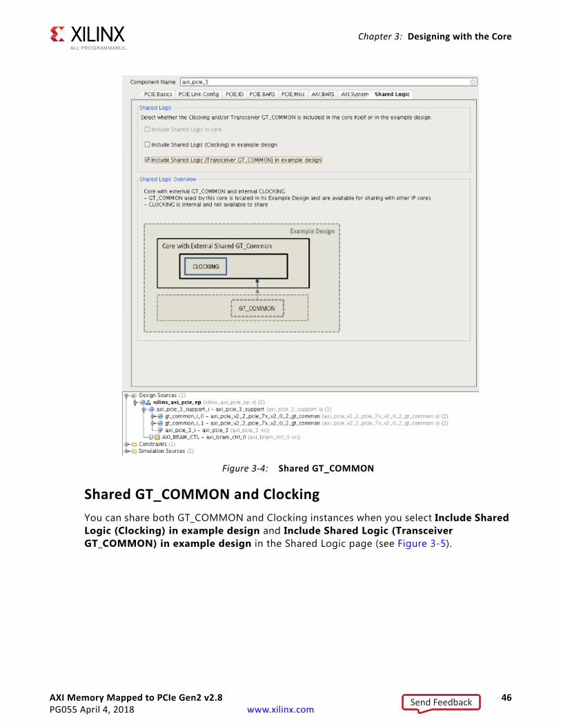
AXI Memory Mapped to PCIe Gen2 v2.8 46PG055 April 4, 2018 www.xilinx.com
Chapter 3: Designing with the Core
Shared GT_COMMON and ClockingYou can share both GT_COMMON and Clocking instances when you select Include Shared Logic (Clocking) in example design and Include Shared Logic (Transceiver GT_COMMON) in example design in the Shared Logic page (see Figure 3-5).
X-Ref Target - Figure 3-4
Figure 3-4: Shared GT_COMMON
Send Feedback
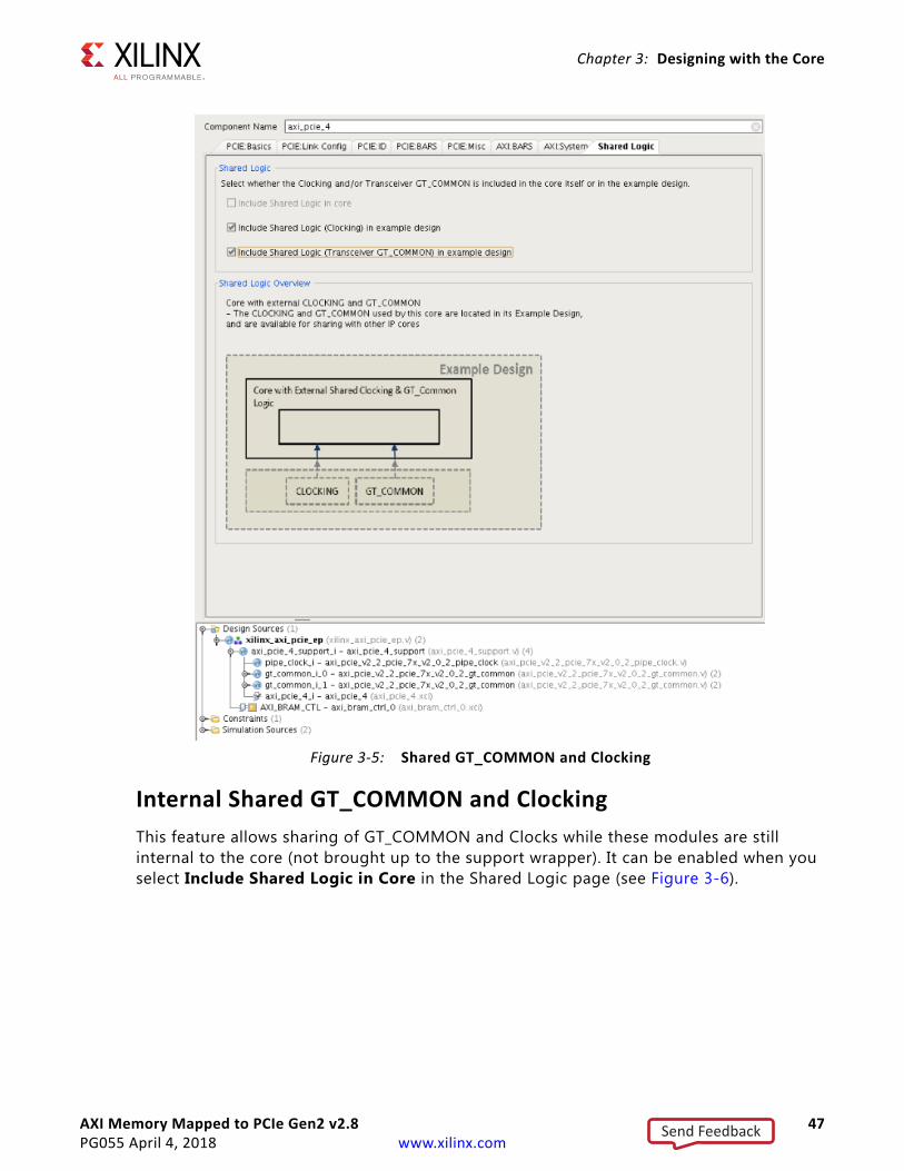
AXI Memory Mapped to PCIe Gen2 v2.8 47PG055 April 4, 2018 www.xilinx.com
Chapter 3: Designing with the Core
Internal Shared GT_COMMON and ClockingThis feature allows sharing of GT_COMMON and Clocks while these modules are still internal to the core (not brought up to the support wrapper). It can be enabled when you select Include Shared Logic in Core in the Shared Logic page (see Figure 3-6).
X-Ref Target - Figure 3-5
Figure 3-5: Shared GT_COMMON and Clocking
Send Feedback
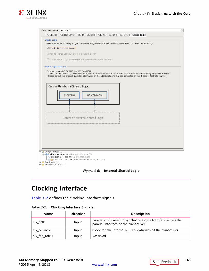
AXI Memory Mapped to PCIe Gen2 v2.8 48PG055 April 4, 2018 www.xilinx.com
Chapter 3: Designing with the Core
Clocking InterfaceTable 3-2 defines the clocking interface signals.
X-Ref Target - Figure 3-6
Figure 3-6: Internal Shared Logic
Table 3-2: Clocking Interface Signals
Name Direction Description
clk_pclk Input Parallel clock used to synchronize data transfers across the parallel interface of the transceiver.
clk_rxusrclk Input Clock for the internal RX PCS datapath of the transceiver.
clk_fab_refclk Input Reserved.
Send Feedback
AXI Memory Mapped to PCIe Gen2 v2.8 49PG055 April 4, 2018 www.xilinx.com
Chapter 3: Designing with the Core
The Clocking architecture is described in detail in the Use Model chapter of the 7 Series FPGAs GTX/GTH Transceivers User Guide (UG476) [Ref 3].
AXI Transactions for PCIeTable 3-3 and Table 3-4 are the translation tables for AXI4-Stream and memory-mapped transactions.
clk_dclk Input GT DRP clock input. This clock is required for proper core operation even when GT DRP interface is not used by the user.
clk_userclk1(1) Input Clock used internally for PCIe block logic.
clk_userclk2(1) Input User clock used for the majority portion of the AXI-PCIe Bridge, AXI4 (axi_aclk_out), and AXI4-Lite (axi_ctl_aclk_out) interfaces.
clk_oobclk_in Input Free running clock used for OOB detect circuitry in the Transceivers
clk_mmcm_lock Input Indicates if the MMCM is locked onto the source clk. This signal is used only when external shared clocking logic is enabled.
clk_txoutclk Output Recommended clock output to the FPGA logic. Frequency of this clock will be equal to the sys_clk frequency.
clk_rxoutclk Output Reserved.
clk_pclk_sel Output Parallel clock select. This signal toggles when PCIe link up-trains to Gen2 speed.
clk_gen3 Output Reserved.
pipe_mmcm_rst_n Input
MMCM reset port. This port could be used by the upper layer to reset MMCM if error recovery is required. If the system detects the deassertion of MMCM lock, Xilinx recommends that you reset the MMCM. The recommended approach is to reset the MMCM after the MMCM input clock recovers (if MMCM reset occurs before the input reference clock recovers, the MMCM might never relock). After MMCM is reset, wait for MMCM to lock and then reset the PIPE Wrapper as normally done. Currently this port is tied High.
Notes: 1. clk_userclk1 and clk_userclk2 are the user clocks for PCIe and AXI related logic and are different than TX/
RXUSRCLK and TX/RXUSRCLK2 referred in 7-series FPGAs GTX/GTH Transceivers User Guide (UG476) [Ref 3]. TX/RXUSRCLK and TX/RXUSRCLK2 referred there are 'user clocks' from the Transceivers perspective which are clk_pclk (Parallel clock).
Table 3-2: Clocking Interface Signals (Cont’d)
Name Direction Description
Send Feedback
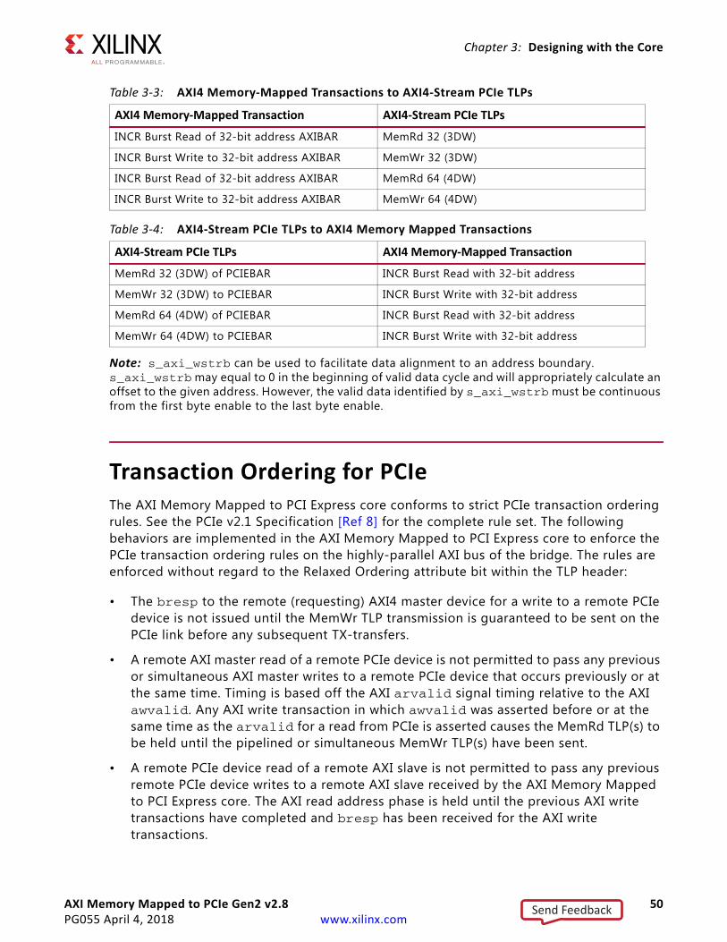
AXI Memory Mapped to PCIe Gen2 v2.8 50PG055 April 4, 2018 www.xilinx.com
Chapter 3: Designing with the Core
Note: s_axi_wstrb can be used to facilitate data alignment to an address boundary. s_axi_wstrb may equal to 0 in the beginning of valid data cycle and will appropriately calculate an offset to the given address. However, the valid data identified by s_axi_wstrb must be continuous from the first byte enable to the last byte enable.
Transaction Ordering for PCIeThe AXI Memory Mapped to PCI Express core conforms to strict PCIe transaction ordering rules. See the PCIe v2.1 Specification [Ref 8] for the complete rule set. The following behaviors are implemented in the AXI Memory Mapped to PCI Express core to enforce the PCIe transaction ordering rules on the highly-parallel AXI bus of the bridge. The rules are enforced without regard to the Relaxed Ordering attribute bit within the TLP header:
• The bresp to the remote (requesting) AXI4 master device for a write to a remote PCIe device is not issued until the MemWr TLP transmission is guaranteed to be sent on the PCIe link before any subsequent TX-transfers.
• A remote AXI master read of a remote PCIe device is not permitted to pass any previous or simultaneous AXI master writes to a remote PCIe device that occurs previously or at the same time. Timing is based off the AXI arvalid signal timing relative to the AXI awvalid. Any AXI write transaction in which awvalid was asserted before or at the same time as the arvalid for a read from PCIe is asserted causes the MemRd TLP(s) to be held until the pipelined or simultaneous MemWr TLP(s) have been sent.
• A remote PCIe device read of a remote AXI slave is not permitted to pass any previous remote PCIe device writes to a remote AXI slave received by the AXI Memory Mapped to PCI Express core. The AXI read address phase is held until the previous AXI write transactions have completed and bresp has been received for the AXI write transactions.
Table 3-3: AXI4 Memory-Mapped Transactions to AXI4-Stream PCIe TLPs
AXI4 Memory-Mapped Transaction AXI4-Stream PCIe TLPs
INCR Burst Read of 32-bit address AXIBAR MemRd 32 (3DW)
INCR Burst Write to 32-bit address AXIBAR MemWr 32 (3DW)
INCR Burst Read of 32-bit address AXIBAR MemRd 64 (4DW)
INCR Burst Write to 32-bit address AXIBAR MemWr 64 (4DW)
Table 3-4: AXI4-Stream PCIe TLPs to AXI4 Memory Mapped Transactions
AXI4-Stream PCIe TLPs AXI4 Memory-Mapped Transaction
MemRd 32 (3DW) of PCIEBAR INCR Burst Read with 32-bit address
MemWr 32 (3DW) to PCIEBAR INCR Burst Write with 32-bit address
MemRd 64 (4DW) of PCIEBAR INCR Burst Read with 32-bit address
MemWr 64 (4DW) to PCIEBAR INCR Burst Write with 32-bit address
Send Feedback
AXI Memory Mapped to PCIe Gen2 v2.8 51PG055 April 4, 2018 www.xilinx.com
Chapter 3: Designing with the Core
• Read completion data received from a remote PCIe device are not permitted to pass any remote PCIe device writes to a remote AXI slave received by the AXI Memory Mapped to PCI Express core prior to the read completion data. The bresp for the AXI write(s) must be received before the completion data is presented on the AXI read data channel.
• Read data from a remote AXI slave is not permitted to pass any remote AXI master writes to a remote PCIe device initiated on the AXI bus prior to or simultaneously with the read data being returned on the AXI bus. Timing is based on the AXI awvalid signal timing relative to the AXI rvalid assertion. Any AXI write transaction in which awvalid was asserted before or simultaneously with the rvalid being asserted up to and including the last data beat, causes the Completion TLP(s) to be held until the pipelined or simultaneous MemWr TLP(s) have been sent.
IMPORTANT: The transaction ordering rules for PCIe might have an impact on data throughput in heavy bidirectional traffic.
BAR and Address Translation
BAR AddressingC_AXIBAR_n and C_AXIBAR_HIGHADDR_n are used to calculate the size of the AXI BAR n and during address translation to PCIe address.
• C_AXIBAR_n provides the low address where AXI BAR n starts and will be regarded as address offset 0x0 when the address is translated.
• C_AXIBAR_HIGHADDR_n is the high address of the last valid byte address of AXI BAR n. (For more details on how the address gets translated, see Address Translation.)
The difference between the two parameters are your AXI BAR n size. These parameters must be set accordingly such that AXI BAR n size is a power of two and must have at least 8 KB and a maximum of 2 GB.
When a packet is sent to the core (outgoing PCIe packets), the packet must have an address that is in the range of C_AXIBAR_n and C_AXIBAR_HIGHADDR_n. Any packet that is received by the core that has an address outside of this range will be responded to with a SLVERR (Slave Error). When IP Integrator is used, these parameters are derived from the Address Editor tab within IP Integrator. The Address Editor sets the AXI Interconnect as well as the core so the address range matches, and the packet is routed to the core only when the packet has an address within the valid range.
Send Feedback
AXI Memory Mapped to PCIe Gen2 v2.8 52PG055 April 4, 2018 www.xilinx.com
Chapter 3: Designing with the Core
Address TranslationThe address space for PCIe is different than AXI address space. To access one address space from another address space requires an address translation process. On the AXI side, the bridge supports mapping to PCIe on up to six 32-bit or 64-bit AXI base address registers (BARs). The generics used to configure the BARs follow.
C_AXIBAR_NUM, C_AXIBAR_n, C_AXIBAR_HIGHADDR_n, C_AXIBAR2PCIEBAR_n and C_AXIBAR_AS_n
where n represents an AXIBAR number from 0 to 5. The bridge for PCIe supports mapping on up to three 64-bit BARs for PCIe. The generics used to configure the BARs are:
C_PCIEBAR_NUM, C_PCIEBAR2AXIBAR_n and C_PCIEBAR_LEN_n
where n represents a particular BAR number for PCIe from 0 to 2.
Note: The C_INCLUDE_BAROFFSET_REG generic allows for dynamic address translation. When this parameter is set to one, the AXIBAR2PCIEBAR_n translation vectors can be changed by using software.
Four examples follow:
• Example 1 (32-bit PCIe Address Mapping) demonstrates how to set up three 32-bit AXI BARs and translate the AXI address to a 32-bit address for PCIe.
• Example 2 (64-bit PCIe Address Mapping) demonstrates how to set up three 64-bit AXI BARs and translate the AXI address to a 64-bit address for PCIe.
• Example 3 demonstrates how to set up two 64-bit PCIe BARs and translate the address for PCIe to an AXI address.
• Example 4 demonstrates how to set up a combination of two 32-bit AXI BARs and two 64 bit AXI BARs, and translate the AXI address to an address for PCIe.
Example 1 (32-bit PCIe Address Mapping)
This example shows the generic settings to set up three independent 32-bit AXI BARs and address translation of AXI addresses to a remote 32-bit address space for PCIe. This setting of AXI BARs does not depend on the BARs for PCIe within the AXI Memory Mapped to PCI Express core.
In this example, where C_AXIBAR_NUM=3, the following assignments for each range are made:
C_AXIBAR_AS_0=0C_AXIBAR_0=0x12340000C_AXI_HIGHADDR_0=0x1234FFFFC_AXIBAR2PCIEBAR_0=0x5671XXXX (Bits 15-0 do not matter as the lower 16-bits hold the actual lower 16-bits of the PCIe address)
Send Feedback

AXI Memory Mapped to PCIe Gen2 v2.8 53PG055 April 4, 2018 www.xilinx.com
Chapter 3: Designing with the Core
C_AXIBAR_AS_1=0C_AXIBAR_1=0xABCDE000C_AXI_HIGHADDR_1=0xABCDFFFFC_AXIBAR2PCIEBAR_1=0xFEDC0XXX (Bits 12-0 do not matter as the lower 13-bits hold the actual lower 13-bits of the PCIe address)
C_AXIBAR_AS_2=0C_AXIBAR_2=0xFE000000C_AXI_HIGHADDR_2=0xFFFFFFFFC_AXIBAR2PCIEBAR_2=0x40XXXXXX (Bits 24-0 do not care)
• Accessing the Bridge AXIBAR_0 with address 0x12340ABC on the AXI bus yields 0x56710ABC on the bus for PCIe.
• Accessing the Bridge AXIBAR_1 with address 0xABCDF123 on the AXI bus yields 0xFEDC1123 on the bus for PCIe.
• Accessing the Bridge AXIBAR_2 with address 0xFFFEDCBA on the AXI bus yields 0x41FEDCBA on the bus for PCIe.
Example 2 (64-bit PCIe Address Mapping)
This example shows the generic settings to set up to three independent 64-bit AXI BARs and address translation of AXI addresses to a remote 64-bit address space for PCIe. This setting of AXI BARs does not depend on the BARs for PCIe within the Bridge.
X-Ref Target - Figure 3-7
Figure 3-7: AXI to PCIe Address Translation
C_AXIBAR_0 =0x12340000
C_AXI_HIGHADDR_0 =0x1234FFFF
C_AXIBAR2PCIEBAR_0 = 0x5671xxxx
0ABC Final PCIe Address =0x56710ABC
+
X12306
AXI AWADDR =0x12340ABC
AXI to PCIe Address Translation
Intermediate Address = 0x0ABC
Send Feedback
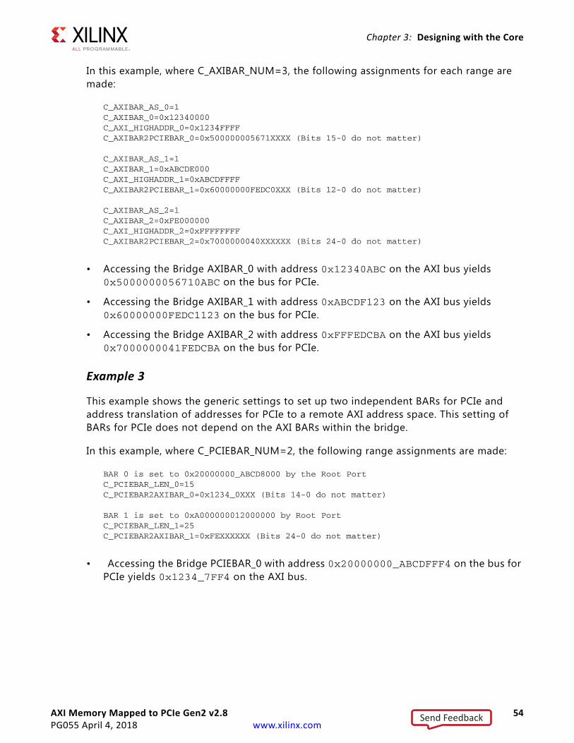
AXI Memory Mapped to PCIe Gen2 v2.8 54PG055 April 4, 2018 www.xilinx.com
Chapter 3: Designing with the Core
In this example, where C_AXIBAR_NUM=3, the following assignments for each range are made:
C_AXIBAR_AS_0=1C_AXIBAR_0=0x12340000C_AXI_HIGHADDR_0=0x1234FFFFC_AXIBAR2PCIEBAR_0=0x500000005671XXXX (Bits 15-0 do not matter)
C_AXIBAR_AS_1=1C_AXIBAR_1=0xABCDE000C_AXI_HIGHADDR_1=0xABCDFFFFC_AXIBAR2PCIEBAR_1=0x60000000FEDC0XXX (Bits 12-0 do not matter)
C_AXIBAR_AS_2=1C_AXIBAR_2=0xFE000000C_AXI_HIGHADDR_2=0xFFFFFFFFC_AXIBAR2PCIEBAR_2=0x7000000040XXXXXX (Bits 24-0 do not matter)
• Accessing the Bridge AXIBAR_0 with address 0x12340ABC on the AXI bus yields 0x5000000056710ABC on the bus for PCIe.
• Accessing the Bridge AXIBAR_1 with address 0xABCDF123 on the AXI bus yields 0x60000000FEDC1123 on the bus for PCIe.
• Accessing the Bridge AXIBAR_2 with address 0xFFFEDCBA on the AXI bus yields 0x7000000041FEDCBA on the bus for PCIe.
Example 3
This example shows the generic settings to set up two independent BARs for PCIe and address translation of addresses for PCIe to a remote AXI address space. This setting of BARs for PCIe does not depend on the AXI BARs within the bridge.
In this example, where C_PCIEBAR_NUM=2, the following range assignments are made:
BAR 0 is set to 0x20000000_ABCD8000 by the Root PortC_PCIEBAR_LEN_0=15C_PCIEBAR2AXIBAR_0=0x1234_0XXX (Bits 14-0 do not matter)
BAR 1 is set to 0xA000000012000000 by Root PortC_PCIEBAR_LEN_1=25C_PCIEBAR2AXIBAR_1=0xFEXXXXXX (Bits 24-0 do not matter)
• Accessing the Bridge PCIEBAR_0 with address 0x20000000_ABCDFFF4 on the bus for PCIe yields 0x1234_7FF4 on the AXI bus.
Send Feedback

AXI Memory Mapped to PCIe Gen2 v2.8 55PG055 April 4, 2018 www.xilinx.com
Chapter 3: Designing with the Core
• Accessing Bridge PCIEBAR_1 with address 0xA00000001235FEDC on the bus for PCIe yields 0xFE35FEDC on the AXI bus.
Example 4
This example shows the generic settings to set up a combination of two independent 32-bit AXI BARs and two independent 64-bit BARs and address translation of AXI addresses to a remote address space for PCIe. This setting of AXI BARs do not depend on the BARs for PCIe within the Bridge.
In this example, where C_AXIBAR_NUM=4, the following assignments for each range are made:
C_AXIBAR_AS_0=0C_AXIBAR_0=0x12340000C_AXI_HIGHADDR_0=0x1234FFFFC_AXIBAR2PCIEBAR_0=0x5671XXXX (Bits 15-0 do not matter)
C_AXIBAR_AS_1=1C_AXIBAR_1=0xABCDE000C_AXI_HIGHADDR_1=0xABCDFFFFC_AXIBAR2PCIEBAR_1=0x50000000FEDC0XXX (Bits 12-0 do not matter)
C_AXIBAR_AS_2=0C_AXIBAR_2=0xFE000000C_AXI_HIGHADDR_2=0xFFFFFFFFC_AXIBAR2PCIEBAR_2=0x40XXXXXX (Bits 24-0 do not matter)
C_AXIBAR_AS_3=1C_AXIBAR_3=0x00000000
X-Ref Target - Figure 3-8
Figure 3-8: PCIe to AXI Translation
PCIe BAR 0 (set by Root Complex) = 0x20000000_ABCD8000
C_PCIEBAR2AXIBAR_0 = 0x12345xxxC_PCIEBAR_LEN_0 = 15
(least significant 15 bits (14:0) provide window)
Final translated AXI Address =0x1234 7FF4
+
X12305
PCI Wr Addr =0x20000000_ABCDFFF4
PCIe to AXI Address Translation
Intermediate Address = 0x7FF4
Send Feedback
AXI Memory Mapped to PCIe Gen2 v2.8 56PG055 April 4, 2018 www.xilinx.com
Chapter 3: Designing with the Core
C_AXI_HIGHADDR_3=0x0000007FC_AXIBAR2PCIEBAR_3=0x600000008765438X (Bits 6-0 do not matter)
• Accessing the Bridge AXIBAR_0 with address 0x12340ABC on the AXI bus yields 0x56710ABC on the bus for PCIe.
• Accessing the Bridge AXIBAR_1 with address 0xABCDF123 on the AXI bus yields 0x50000000FEDC1123 on the bus for PCIe.
• Accessing the Bridge AXIBAR_2 with address 0xFFFEDCBA on the AXI bus yields 0x41FEDCBA on the bus for PCIe.
• Accessing the AXI M S PCIe Bridge AXIBAR_3 with address 0x00000071 on the AXI bus yields 0x60000000876543F1 on the bus for PCIe.
Addressing Checks
When setting the following parameters for PCIe address mapping, C_PCIEBAR2AXIBAR_n and C_PCIEBAR_LEN_n, be sure these are set to allow for the 32-bit addressing space on the AXI system. For example, the following setting is illegal and results in an invalid AXI address.
C_PCIEBAR2AXIBAR_0 = 0xFFFF_0000C_PCIEBAR_LEN_0 = 23
Also, check for a larger value on C_PCIEBAR_LEN_n compared to the value assigned to parameter, C_PCIEBAR2AXIBAR_n. For example, the following parameter settings.
C_PCIEBAR2AXIBAR_0 = 0xFFFF_E000C_PCIEBAR_LEN_0 = 20
To keep the AXIBAR upper address bits as 0xFFFF_E000 (to reference bits [31:13]), the C_PCIEBAR_LEN_0 parameter must be set to 13.
InterruptsThis section describes the interrupt pins which include Local, MSI and Legacy Interrupts.
Local InterruptsThe interrupt_out pin can be configured to send interrupts based on the settings of the Interrupt Mask register. The interrupt_out pin signals interrupts to devices attached to the memory mapped AXI4 side of the bridge. The MSI interrupt defined in the Interrupt Mask & Interrupt Decode registers is used to indicate the receipt of a Message Signaled Interrupt only when the bridge is operating in Root Port mode (C_INCLUDE_RC=1).
Send Feedback
AXI Memory Mapped to PCIe Gen2 v2.8 57PG055 April 4, 2018 www.xilinx.com
Chapter 3: Designing with the Core
MSI InterruptWhen the msi_enable output pin indicates that the bridge has Endpoint MSI functionality enabled (msi_enable = 1), the intx_msi_request input pin is defined as MSI_Request and can be used to trigger a Message Signaled Interrupt through a special MemWr TLP to an external Root Port for PCIe on the PCIe side of the Bridge. The intx_msi_request input pin is positive-edge detected and synchronous to axi_aclk_out. The address and data contained in this MemWr TLP are determined by an external Root Port for PCIe configuration of registers within the integrated block for PCI Express. The intx_msi_request pin input is valid only when the bridge is operating in Endpoint mode (C_INCLUDE_RC=0).
Additional MSI capability now supports multiple vectors on the Endpoint configuration of the AXI Memory Mapped to PCI Express core. Using the handshaking described here, an additional input value specifies the vector number to send with the MSI MemWr TLP upstream to the Root Port. This is specified on the input signal, msi_vector_num. This signal is (4:0), and represents up to (32), the allowable MSI messages that can be sent from the Endpoint (and what is enabled after configuration).
The bridge ignores any bits set on the msi_vector_num input signal, if they are not allocated in the Message Control Register.
The Endpoint requests the number of message as specified in the design parameter (of the AXI Memory Mapped to PCI Express), C_NUM_MSI_REQ. Following specification requirements, this parameter can be set up to 5. C_NUM_MSI_REQ represents the number of MSI vectors requested. For example, C_NUM_MSI_REQ = 5 represents a request of 25 = 32 MSI vectors. This parameter value, C_NUM_MSI_REQ is assigned to the Message Control Register field, Multiple Message Capable, bits (3:1).
After configuration, the number of allocated MSI vectors is specified in the design output port, msi_vector_width. This signal with width, (2:0), can only be values up to 5 (101), representing 32 allocated MSI vectors for the Endpoint. Output values of 6 and 7; 110 and 111 are reserved. The msi_vector_width output signal is a direct correlation from the value in the Multiple Message Enable field bits (6:4) of the Message Control Register as shown in Table 3-5.
Table 3-5: MSI Vectors Enabled in Message Control Register
Value Number of Messages Requested Output Signal, MSI_Vector_Width (2:0)
000 1 000
001 2 001
010 4 010
011 8 011
100 16 100
101 32 101
Send Feedback
AXI Memory Mapped to PCIe Gen2 v2.8 58PG055 April 4, 2018 www.xilinx.com
Chapter 3: Designing with the Core
Additional IP is required in the Endpoint PCIe system to create the priority scheme for the MSI vectors on the PCIe interface.
Legacy InterruptsThe bridge supports legacy interrupts for PCI if selected by the C_INTERRUPT_PIN parameter. (Can only be set to 1 when C_INCLUDE_RC = 0.) A value of 1 selects INTA, as defined in Table 2-2. If a legacy interrupt for PCI support is selected and the msi_enable output pin indicates that the bridge has endpoint MSI functionality disabled (MSI_enable = 0), the intx_msi_request pin is defined as INTX. When the INTX pin goes High, an assert INTA message is sent. When the INTX pin goes Low, a deassert INTA message is sent. The interrupts needs to be synchronized to axi_aclk_out. These messages are defined in the PCI 2.1 specification. The intx_msi_request pin input is valid only when the bridge is operating in Endpoint mode (C_INCLUDE_RC=0).
Malformed TLPThe integrated block for PCI Express detects a malformed TLP. For the IP configured as an Endpoint core, a malformed TLP results in a fatal error message being sent upstream if error reporting is enabled in the Device Control Register.
For the IP configured as a Root Port, when a malformed TLP is received from the Endpoint, this can fall under one of several types of violations as per the PCIe specification. For example, if a Received TLP has the Error Poison bit set, this is discarded by the MM/S master bridge, and the MEP (Master Error Poison) bit is set in the Interrupt Decode register.
Abnormal ConditionsThis section describes how the Slave side (Table 3-6) and Master side (Table 3-7) of the AXI Memory Mapped to PCI Express core handle abnormal conditions.
Slave Bridge Abnormal ConditionsSlave bridge abnormal conditions are classified as: Illegal Burst Type and Completion TLP Errors. The following sections describe the manner in which the Bridge handles these errors.
110 Reserved N/A
111 Reserved N/A
Table 3-5: MSI Vectors Enabled in Message Control Register (Cont’d)
Value Number of Messages Requested Output Signal, MSI_Vector_Width (2:0)
Send Feedback

AXI Memory Mapped to PCIe Gen2 v2.8 59PG055 April 4, 2018 www.xilinx.com
Chapter 3: Designing with the Core
Illegal Burst Type
The slave bridge monitors AXI read and write burst type inputs to ensure that only the INCR (incrementing burst) type is requested. Any other value on these inputs is treated as an error condition and the Slave Illegal Burst (SIB) interrupt is asserted. In the case of a read request, the Bridge asserts SLVERR for all data beats and arbitrary data is placed on the s_axi_rdata bus. In the case of a write request, the Bridge asserts SLVERR for the write response and all write data is discarded.
Completion TLP Errors
Any request to the bus for PCIe (except for posted Memory write) requires a completion TLP to complete the associated AXI request. The Slave side of the Bridge checks the received completion TLPs for errors and checks for completion TLPs that are never returned (Completion Timeout). Each of the completion TLP error types are discussed in the subsequent sections.
Unexpected Completion
When the slave bridge receives a completion TLP, it matches the header RequesterID and Tag to the outstanding RequesterID and Tag. A match failure indicates the TLP is an Unexpected Completion which results in the completion TLP being discarded and a Slave Unexpected Completion (SUC) interrupt strobe being asserted. Normal operation then continues.
Unsupported Request
A device for PCIe might not be capable of satisfying a specific read request. For example, the read request targets an unsupported address for PCIe causing the completer to return a completion TLP with a completion status of 0b001 - Unsupported Request. The completer can also return a completion TLP with a completion status that is reserved according to the 2.1 PCIe Specification, which must be treated as an unsupported request status. When the slave bridge receives an unsupported request response, the Slave Unsupported Request (SUR) interrupt is asserted and the SLVERR response is asserted with arbitrary data on the memory mapped AXI4 bus.
Completion Timeout
A Completion Timeout occurs when a completion (Cpl) or completion with data (CplD) TLP is not returned after an AXI to PCIe read request. Completions must complete within the C_COMP_TIMEOUT parameter selected value from the time the MemRd for PCIe request is issued. When a completion timeout occurs, a Slave Completion Timeout (SCT) interrupt is asserted and the SLVERR response is asserted with arbitrary data on the memory mapped AXI4 bus.
Send Feedback

AXI Memory Mapped to PCIe Gen2 v2.8 60PG055 April 4, 2018 www.xilinx.com
Chapter 3: Designing with the Core
Poison Bit Received on Completion Packet
An Error Poison occurs when the completion TLP EP bit is set, indicating that there is poisoned data in the payload. When the slave bridge detects the poisoned packet, the Slave Error Poison (SEP) interrupt is asserted and the SLVERR response is asserted with arbitrary data on the memory mapped AXI4 bus.
Completer Abort
A Completer Abort occurs when the completion TLP completion status is 0b100 - Completer Abort. This indicates that the completer has encountered a state in which it was unable to complete the transaction. When the slave bridge receives a completer abort response, the Slave Completer Abort (SCA) interrupt is asserted and the SLVERR response is asserted with arbitrary data on the memory mapped AXI4 bus.
Master Bridge Abnormal ConditionsThe following sections describe the manner in which the master bridge handles abnormal conditions.
AXI DECERR Response
When the master bridge receives a DECERR response from the AXI bus, the request is discarded and the Master DECERR (MDE) interrupt is asserted. If the request was
Table 3-6: Slave Bridge Response to Abnormal Conditions
Transfer Type Abnormal Condition Bridge Response
Read Illegal burst typeSIB interrupt is asserted.
SLVERR response given with arbitrary read data.
Write Illegal burst type
SIB interrupt is asserted.
Write data is discarded.
SLVERR response given.
Read Unexpected completionSUC interrupt is asserted.
Completion is discarded.
Read Unsupported Request status returned
SUR interrupt is asserted.
SLVERR response given with arbitrary read data.
Read Completion timeoutSCT interrupt is asserted.
SLVERR response given with arbitrary read data.
Read Poison bit in completion
Completion data is discarded.
SEP interrupt is asserted.
SLVERR response given with arbitrary read data.
Read Completer Abort (CA) status returned
SCA interrupt is asserted.
SLVERR response given with arbitrary read data.
Send Feedback
AXI Memory Mapped to PCIe Gen2 v2.8 61PG055 April 4, 2018 www.xilinx.com
Chapter 3: Designing with the Core
non-posted, a completion packet with the Completion Status = Unsupported Request (UR) is returned on the bus for PCIe.
AXI SLVERR Response
When the master bridge receives a SLVERR response from the addressed AXI slave, the request is discarded and the Master SLVERR (MSE) interrupt is asserted. If the request was non-posted, a completion packet with the Completion Status = Completer Abort (CA) is returned on the bus for PCIe.
Max Payload Size for PCIe, Max Read Request Size or 4K Page Violated
It is the responsibility of the requester to ensure that the outbound request adhere to the Max Payload Size, Max Read Request Size, and 4 Kb Page Violation rules. If the master bridge receives a request that violates one of these rules, the bridge processes the invalid request as a valid request, which can return a completion that violates one of these conditions or can result in the loss of data. The master bridge does not return a malformed TLP completion to signal this violation.
Completion Packets
When the MAX_READ_REQUEST_SIZE is greater than the MAX_PAYLOAD_SIZE, a read request for PCIe can ask for more data than the master bridge can insert into a single completion packet. When this situation occurs, multiple completion packets are generated up to MAX_PAYLOAD_SIZE, with the Read Completion Boundary (RCB) observed.
Poison Bit
When the poison bit is set in a transaction layer packet (TLP) header, the payload following the header is corrupted. When the master bridge receives a memory request TLP with the poison bit set, it discards the TLP and asserts the Master Error Poison (MEP) interrupt strobe.
Zero Length Requests
When the master bridge receives a read request with the Length = 0x1, FirstBE = 0x00, and LastBE = 0x00, it responds by sending a completion with Status = Successful Completion. When the master bridge receives a write request with the Length = 0x1, FirstBE = 0x00, and LastBE = 0x00 there is no effect.
Table 3-7: Master Bridge Response to Abnormal Conditions
Transfer Type Abnormal Condition Bridge Response
Read DECERR responseMDE interrupt strobe asserted.
Completion returned with Unsupported Request status.
Write DECERR response MDE interrupt strobe asserted.
Send Feedback

AXI Memory Mapped to PCIe Gen2 v2.8 62PG055 April 4, 2018 www.xilinx.com
Chapter 3: Designing with the Core
Link Down BehaviorThe normal operation of the AXI Memory Mapped to PCI Express core is dependent on the integrated block for PCIe establishing and maintaining the point-to-point link with an external device for PCIe. If the link has been lost, it must be re-established to return to normal operation.
When a Hot Reset is received by the AXI Memory Mapped to PCI Express core, the link goes down and the PCI Configuration Space must be reconfigured.
Initiated AXI4 write transactions that have not yet completed on the AXI4 bus when the link goes down have a SLVERR response given and the write data is discarded. Initiated AXI4 read transactions that have not yet completed on the AXI4 bus when the link goes down have a SLVERR response given, with arbitrary read data returned.
Any MemWr TLPs for PCIe that have been received, but the associated AXI4 write transaction has not started when the link goes down, are discarded. If the associated AXI4 write transaction is in the process of being transferred, it completes as normal. Any MemRd TLPs for PCIe that have been received, but have not returned completion TLPs by the time the link goes down, complete on the AXI4 bus, but do not return completion TLPs on the PCIe bus.
Root PortWhen configured to support Root Port functionality, the AXI Memory Mapped to PCI Express core fully supports Root Port operation as supported by the underlying block. There are a few details that need special consideration. The following subsections contain information and design considerations about Root Port support.
Read SLVERR responseMSE interrupt strobe asserted.
Completion returned with Completer Abort status.
Write SLVERR response MSE interrupt strobe asserted.
Write Poison bit set in requestMEP interrupt strobe asserted.
Data is discarded.
Read DECERR responseMDE interrupt strobe asserted.
Completion returned with Unsupported Request status.
Write DECERR response MDE interrupt strobe asserted.
Table 3-7: Master Bridge Response to Abnormal Conditions
Transfer Type Abnormal Condition Bridge Response
Send Feedback
AXI Memory Mapped to PCIe Gen2 v2.8 63PG055 April 4, 2018 www.xilinx.com
Chapter 3: Designing with the Core
Power Limit Message TLPThe AXI Memory Mapped to PCI Express core automatically sends a Power Limit Message TLP when the Master Enable bit of the Command Register is set. The software must set the Requester ID register before setting the Master Enable bit to ensure that the desired Requester ID is used in the Message TLP.
Root Port Configuration ReadWhen an ECAM access is performed to the primary bus number, self-configuration of the integrated block for PCIe is performed. A PCIe configuration transaction is not performed and is not presented on the link. When an ECAM access is performed to the bus number that is equal to the secondary bus value in the Enhanced PCIe type 1 configuration header, then type 0 configuration transactions are generated.
When an ECAM access is attempted to a bus number that is in the range defined by the secondary bus number and subordinate bus number range (not including secondary bus number), then type 1 configuration transactions are generated. The primary, secondary and subordinate bus numbers are written and updated by Root Port software to the type 1 PCI Configuration Header of the AXI Memory Mapped to PCI Express core in the enumeration procedure.
When an ECAM access is attempted to a bus number that is out of the range defined by the secondary bus_number and subordinate bus number, the bridge does not generate a configuration request and signal a SLVERR response on the AXI4-Lite bus.
When a Unsupported Request (UR) response is received for a configuration read request, all ones are returned on the AXI4-Lite bus to signify that a device does not exist at the requested device address. It is the responsibility of the software to ensure configuration write requests are not performed to device addresses that do not exist. However, the AXI Memory Mapped to PCI Express core asserts SLVERR response on the AXI4-Lite bus when a configuration write request is performed on device addresses that do not exist or a UR response is received.
Root Port BARDuring core customization in the Vivado Design Suite, select the Hide RP BAR option to force the core to return zeros when User Logic or CPU is probing the RP BAR0 register and to mask any write to this register to prevent any address from being allocated for Root Port BAR. The base address then defaults to 0x0000_0000.
When BAR 64 bit Enabled is selected, the maximum BAR size for Root Port configuration is 4 GB. This option allows all 32-bits of AXI addresses to be addressable from the PCIe link. Inherently, AXI-PCIe BAR translation is then disabled when 4 GB is selected.
Send Feedback
AXI Memory Mapped to PCIe Gen2 v2.8 64PG055 April 4, 2018 www.xilinx.com
Chapter 3: Designing with the Core
BAR 0 cannot be disabled. If a system must have no BAR for Root Port and accepts all incoming packets, select Hide RP BAR, select BAR 64 bit Enabled, and set the Bar 0 size to 4 Gigabytes.
The Root Port BAR customization options in the Vivado Design Suite are found in PCIe Base Address Registers in Chapter 4.
Unsupported Request to Upstream TrafficTo receive upstream traffic from a connected device, the Root Ports PCIe BAR_0 must be configured. If BAR_0 is not configured, the Root Port responds to requests with a Completion returned with Unsupported Request status.
Configuration Transaction TimeoutConfiguration transactions are non-posted transactions. The AXI Memory Mapped to PCI Express core has a timer for timeout termination of configuration transactions that have not completed on the PCIe link. SLVERR is returned when a configuration timeout occurs. Timeout of configuration transactions are flagged by an interrupt as well.
Abnormal Configuration Transaction Termination ResponsesResponses on AXI4-Lite to abnormal terminations to configuration transactions are shown in Table 3-8.
Table 3-8: Responses of AXI Memory Mapped to PCI Express to Abnormal Configuration Terminations
Transfer Type Abnormal Condition Bridge Response
Config Read or Write Bus number not in the range of primary bus number through subordinate bus number. SLVERR response is asserted.
Config Read or Write Valid bus number and completion timeout occurs. SLVERR response is asserted.
Config Read or Write Completion timeout. SLVERR response is asserted.
Config Write Bus number in the range of secondary bus number through subordinate bus number and UR is returned. SLVERR response is asserted.
Send Feedback

AXI Memory Mapped to PCIe Gen2 v2.8 65PG055 April 4, 2018 www.xilinx.com
Chapter 4
Design Flow StepsThis chapter describes customizing and generating the core, constraining the core, and the simulation, synthesis and implementation steps that are specific to this IP core. More detailed information about the Vivado® design flows and the Vivado IP integrator can be found in the following Vivado Design Suite user guides:
• Vivado Design Suite User Guide: Designing IP Subsystems using IP Integrator (UG994) [Ref 15]
• Vivado Design Suite User Guide: Designing with IP (UG896) [Ref 12]
• Vivado Design Suite User Guide: Getting Started (UG910) [Ref 11]
• Vivado Design Suite User Guide: Logic Simulation (UG900) [Ref 13]
Customizing and Generating the CoreThis section includes information about using the Vivado Design Suite to customize and generate the core.
Note: If you are customizing and generating the core in the Vivado IP integrator, see the Vivado Design Suite User Guide: Designing IP Subsystems using IP Integrator (UG994) [Ref 15] for detailed information. IP integrator might auto-compute certain configuration values when validating or generating the design. To check whether the values do change, see the description of the parameter in this chapter. To view the parameter value you can run the validate_bd_design command in the Tcl Console.
You can customize the IP for use in your design by specifying values for the various parameters associated with the IP core using the following steps:
1. Select the IP from the IP catalog.
2. Double-click the selected IP, or select the Customize IP command from the toolbar or right-click menu.
Send Feedback
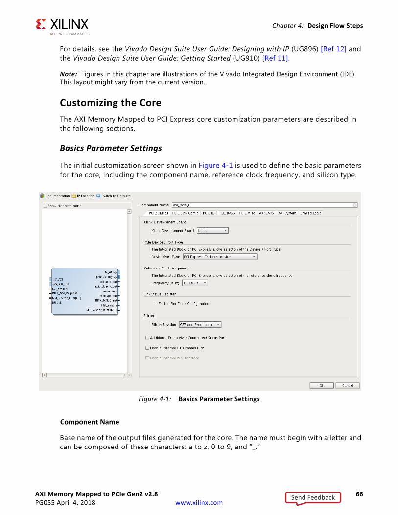
AXI Memory Mapped to PCIe Gen2 v2.8 66PG055 April 4, 2018 www.xilinx.com
Chapter 4: Design Flow Steps
For details, see the Vivado Design Suite User Guide: Designing with IP (UG896) [Ref 12] and the Vivado Design Suite User Guide: Getting Started (UG910) [Ref 11].
Note: Figures in this chapter are illustrations of the Vivado Integrated Design Environment (IDE). This layout might vary from the current version.
Customizing the Core The AXI Memory Mapped to PCI Express core customization parameters are described in the following sections.
Basics Parameter Settings
The initial customization screen shown in Figure 4-1 is used to define the basic parameters for the core, including the component name, reference clock frequency, and silicon type.
Component Name
Base name of the output files generated for the core. The name must begin with a letter and can be composed of these characters: a to z, 0 to 9, and “_.”
X-Ref Target - Figure 4-1
Figure 4-1: Basics Parameter Settings
Send Feedback

AXI Memory Mapped to PCIe Gen2 v2.8 67PG055 April 4, 2018 www.xilinx.com
Chapter 4: Design Flow Steps
IMPORTANT: The name cannot be the same as a core module name; for example, "axi_pcie" is a reserved name.
PCIe Device/Port Type
Indicates the PCI Express logical device type.
Reference Clock Frequency
Selects the frequency of the reference clock provided on the refclk input.
Slot Clock Configuration
Enables the Slot Clock Configuration bit in the Link Status register. Selecting this option means the link is synchronously clocked. See Clocking, page 40 for more information on clocking options.
Silicon Type
Selects the silicon type.
Additional Transceiver Control and Status Ports
When this option is checked, the transceiver debug ports are enabled. See Table B-1 for a list of these ports.
Enable External GT Channel DRP
The external GT channel DRP ports are pulled out to the core top.
• ext_ch_gt_drpdo[15:0]
• ext_ch_gt_drpdi[15:0]
• ext_ch_gt_drpen[0:0]
• ext_ch_gt_drwe[0:0]
• ext_ch_gt_drprdy[:0]
• ext_ch_gt_drpaddr[8:0]
gt_ch_drp_rdy indicates that the external GT channel DRP is ready to use, and that it is not in use by internal logic.
Enable External PIPE Interface
When selected, this option enables an external third-party bus functional Model (BFM) to connect to the PIPE interface of the AXI PCIe core. Note that this option is disabled by default and is enabled when the Include Shared Logic (Clocking) in example design
Send Feedback

AXI Memory Mapped to PCIe Gen2 v2.8 68PG055 April 4, 2018 www.xilinx.com
Chapter 4: Design Flow Steps
option is selected in the Shared Logic page of the Vivado IDE. This is applicable for both Endpoint and Root Port configurations.
PCIe Link Configuration
The PCIe Link Config page is shown in Figure 4-2.
Number of Lanes
The AXI Memory Mapped to PCI Express® core requires the selection of the initial lane width. Table 4-1 defines the available widths and associated generated core. Wider lane width cores can train down to smaller lane widths if attached to a smaller lane-width device.
X-Ref Target - Figure 4-2
Figure 4-2: PCIe Link Configuration
Table 4-1: Lane Width and Product Generated
Lane Width Product Generated
x1 1-Lane
x2 2-Lane
x4 4-Lane
x8 8-Lane
Send Feedback
AXI Memory Mapped to PCIe Gen2 v2.8 69PG055 April 4, 2018 www.xilinx.com
Chapter 4: Design Flow Steps
Link Speed
The AXI Memory Mapped to PCI Express core allows you to select the maximum link speed supported by the device. Table 4-2 defines the lane widths and link speeds supported by the device. Higher link speed cores are capable of training to a lower link speed if connected to a lower link speed capable device.
PCIe Block Location
The AXI Memory Mapped to PCI Express core allows you to select the PCI Express Hard Block within Xilinx FPGAs.
PCIe ID Settings
The Identity Settings pages are shown in Figure 4-3. These settings customize the IP initial values and device class code.
Table 4-2: Lane Width and Link Speed
Lane Width Link Speed
x1 2.5 Gb/s, 5 Gb/s
x2 2.5 Gb/s, 5 Gb/s
x4 2.5 Gb/s, 5 Gb/s
x8 2.5 Gb/s, 5 Gb/s
Send Feedback
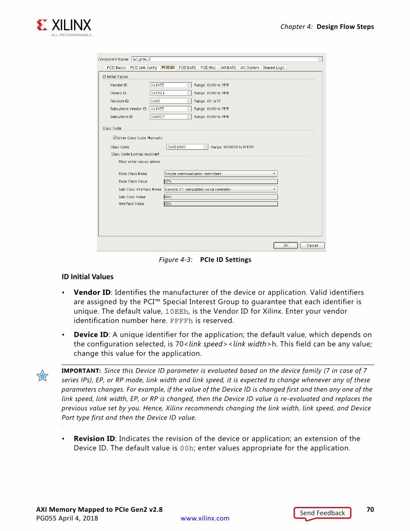
AXI Memory Mapped to PCIe Gen2 v2.8 70PG055 April 4, 2018 www.xilinx.com
Chapter 4: Design Flow Steps
ID Initial Values
• Vendor ID: Identifies the manufacturer of the device or application. Valid identifiers are assigned by the PCI™ Special Interest Group to guarantee that each identifier is unique. The default value, 10EEh, is the Vendor ID for Xilinx. Enter your vendor identification number here. FFFFh is reserved.
• Device ID: A unique identifier for the application; the default value, which depends on the configuration selected, is 70<link speed><link width>h. This field can be any value; change this value for the application.
IMPORTANT: Since this Device ID parameter is evaluated based on the device family (7 in case of 7 series IPs), EP, or RP mode, link width and link speed, it is expected to change whenever any of these parameters changes. For example, if the value of the Device ID is changed first and then any one of the link speed, link width, EP, or RP is changed, then the Device ID value is re-evaluated and replaces the previous value set by you. Hence, Xilinx recommends changing the link width, link speed, and Device Port type first and then the Device ID value.
• Revision ID: Indicates the revision of the device or application; an extension of the Device ID. The default value is 00h; enter values appropriate for the application.
X-Ref Target - Figure 4-3
Figure 4-3: PCIe ID Settings
Send Feedback
AXI Memory Mapped to PCIe Gen2 v2.8 71PG055 April 4, 2018 www.xilinx.com
Chapter 4: Design Flow Steps
• Subsystem Vendor ID: Further qualifies the manufacturer of the device or application. Enter a Subsystem Vendor ID here; the default value is 10EEh. Typically, this value is the same as Vendor ID. Setting the value to 0000h can cause compliance testing issues.
• Subsystem ID: Further qualifies the manufacturer of the device or application. This value is typically the same as the Device ID; the default value depends on the lane width and link speed selected. Setting the value to 0000h can cause compliance testing issues.
Class Code
The Class Code identifies the general function of a device, and is divided into three byte-size fields. The Vivado IDE allows you to either enter the 24-bit value manually (default) by either selecting the Enter Class Code Manually checkbox or using the Class Code lookup assistant to populate the field. De-select the checkbox to enable the Class Code assistant.
• Base Class: Broadly identifies the type of function performed by the device.
• Sub-Class: More specifically identifies the device function.
• Interface: Defines a specific register-level programming interface, if any, allowing device-independent software to interface with the device.
Class code encoding can be found in the PCI-SIG® specifications [Ref 8].
Class Code Look-up Assistant
The Class Code Look-up Assistant provides the Base Class, Sub-Class and Interface values for a selected general function of a device. This Look-up Assistant tool only displays the three values for a selected function. You must enter the values in Class Code for these values to be translated into device settings.
PCIe Base Address Registers
The PCIe Base Address Registers (BARs) screen shown in Figure 4-4 set the base address register space for the Endpoint configuration. Each BAR (0 through 5) configures the BAR Aperture Size and Control attributes of the Physical Function, as described in Table 4-3.
Send Feedback

AXI Memory Mapped to PCIe Gen2 v2.8 72PG055 April 4, 2018 www.xilinx.com
Chapter 4: Design Flow Steps
Base Address Register Overview
The AXI Memory Mapped to PCI Express core in Endpoint configuration supports up to three 32-bit BARs or three 64-bit BARs. The AXI Memory Mapped to PCI Express in Root Port configuration supports one 32-bit BARs or one 64-bit BAR.
All BAR registers share these options:
• Checkbox: Click the checkbox to enable BAR. Deselect the checkbox to disable BAR.
• Type: BARs can be Memory apertures only. Memory BARs can be either 64-bit or 32-bit. Prefetch is enabled for 64-bit and not enabled for 32-bit. When a BAR is set as 64 bits, it uses the next BAR for the extended address space, making it inaccessible.
• Size: The available Size range depends on the PCIe® Device/Port Type and the Type of BAR selected. Table 4-3 lists the available BAR size ranges.
X-Ref Target - Figure 4-4
Figure 4-4: PCIe Base Address Register
Table 4-3: BAR Size Ranges for Device Configuration
PCIe Device/Port Type BAR Type BAR Size Range
PCI Express Endpoint32-bit Memory 8 KB - 2 GB
64-bit Memory 8 KB - 2 GB
Root Port of PCI Express Root Complex
32-bit Memory 8 KB - 2 GB
64-bit Memory 8 KB - 4 GB
Send Feedback
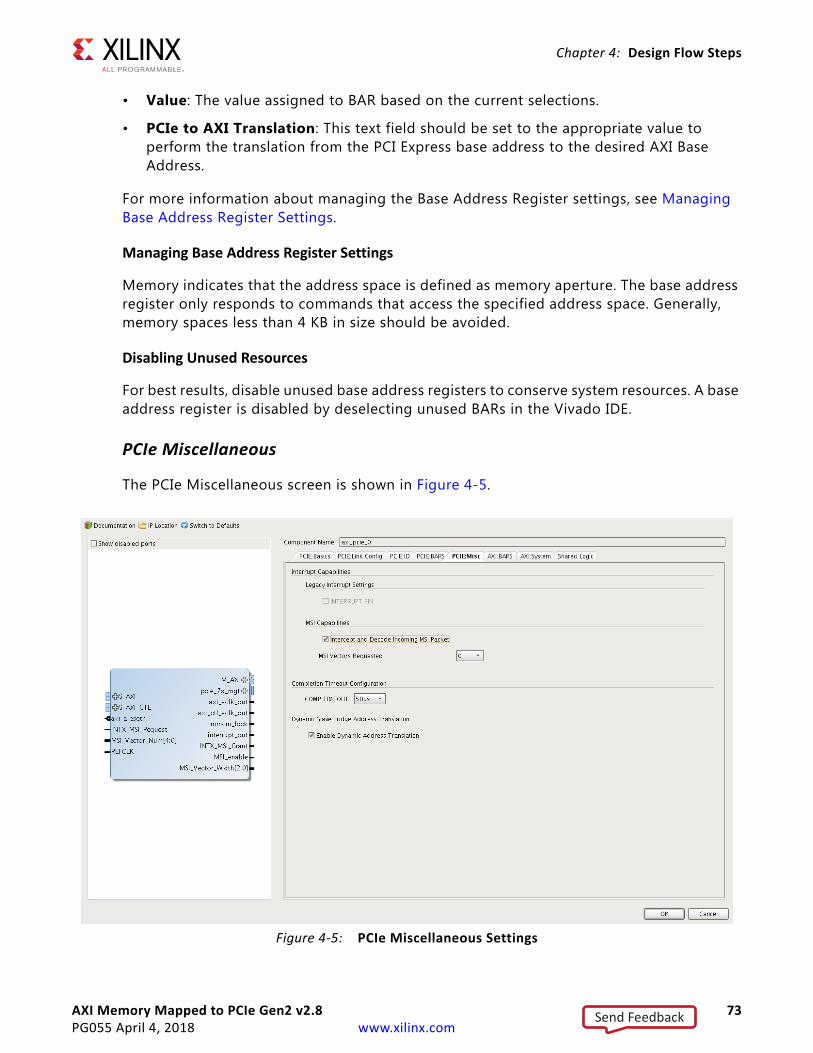
AXI Memory Mapped to PCIe Gen2 v2.8 73PG055 April 4, 2018 www.xilinx.com
Chapter 4: Design Flow Steps
• Value: The value assigned to BAR based on the current selections.
• PCIe to AXI Translation: This text field should be set to the appropriate value to perform the translation from the PCI Express base address to the desired AXI Base Address.
For more information about managing the Base Address Register settings, see Managing Base Address Register Settings.
Managing Base Address Register Settings
Memory indicates that the address space is defined as memory aperture. The base address register only responds to commands that access the specified address space. Generally, memory spaces less than 4 KB in size should be avoided.
Disabling Unused Resources
For best results, disable unused base address registers to conserve system resources. A base address register is disabled by deselecting unused BARs in the Vivado IDE.
PCIe Miscellaneous
The PCIe Miscellaneous screen is shown in Figure 4-5.
X-Ref Target - Figure 4-5
Figure 4-5: PCIe Miscellaneous Settings
Send Feedback
AXI Memory Mapped to PCIe Gen2 v2.8 74PG055 April 4, 2018 www.xilinx.com
Chapter 4: Design Flow Steps
Interrupt Pin
Indicates the usage of Legacy interrupts.The AXI Memory Mapped to PCI Express core implements INTA only.
Intercept and Decode Incoming MSI Packet
Indicates that a received Memory Write packet with an address equal to the value of Root Port MSI Base register will be decoded and reported as an MSI interrupt in the Root Port Interrupt FIFO register.
MSI Vectors Requested
Indicates the number of MSI vectors requested by the core.
Completion Timeout Configuration
Indicates the completion timeout value for incoming completions due to outstanding memory read requests.
Dynamic Slave Bridge Address Translation
Enables the address translation vectors within the AXI Memory Mapped to PCI Express bridge logic to be changed dynamically through the AXI4-Lite interface.
AXI Base Address Registers
The AXI Base Address Registers (BARs) screen shown in Figure 4-6 sets the AXI base address registers and the translation between AXI Memory space and PCI Express Memory space. Each BAR has a Base Address, High Address, and translation field which can be configured through the Vivado IDE.
Send Feedback
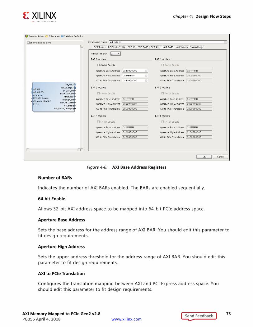
AXI Memory Mapped to PCIe Gen2 v2.8 75PG055 April 4, 2018 www.xilinx.com
Chapter 4: Design Flow Steps
Number of BARs
Indicates the number of AXI BARs enabled. The BARs are enabled sequentially.
64-bit Enable
Allows 32-bit AXI address space to be mapped into 64-bit PCIe address space.
Aperture Base Address
Sets the base address for the address range of AXI BAR. You should edit this parameter to fit design requirements.
Aperture High Address
Sets the upper address threshold for the address range of AXI BAR. You should edit this parameter to fit design requirements.
AXI to PCIe Translation
Configures the translation mapping between AXI and PCI Express address space. You should edit this parameter to fit design requirements.
X-Ref Target - Figure 4-6
Figure 4-6: AXI Base Address Registers
Send Feedback
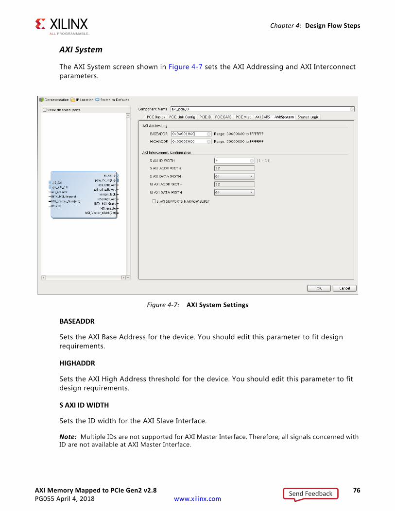
AXI Memory Mapped to PCIe Gen2 v2.8 76PG055 April 4, 2018 www.xilinx.com
Chapter 4: Design Flow Steps
AXI System
The AXI System screen shown in Figure 4-7 sets the AXI Addressing and AXI Interconnect parameters.
BASEADDR
Sets the AXI Base Address for the device. You should edit this parameter to fit design requirements.
HIGHADDR
Sets the AXI High Address threshold for the device. You should edit this parameter to fit design requirements.
S AXI ID WIDTH
Sets the ID width for the AXI Slave Interface.
Note: Multiple IDs are not supported for AXI Master Interface. Therefore, all signals concerned with ID are not available at AXI Master Interface.
X-Ref Target - Figure 4-7
Figure 4-7: AXI System Settings
Send Feedback
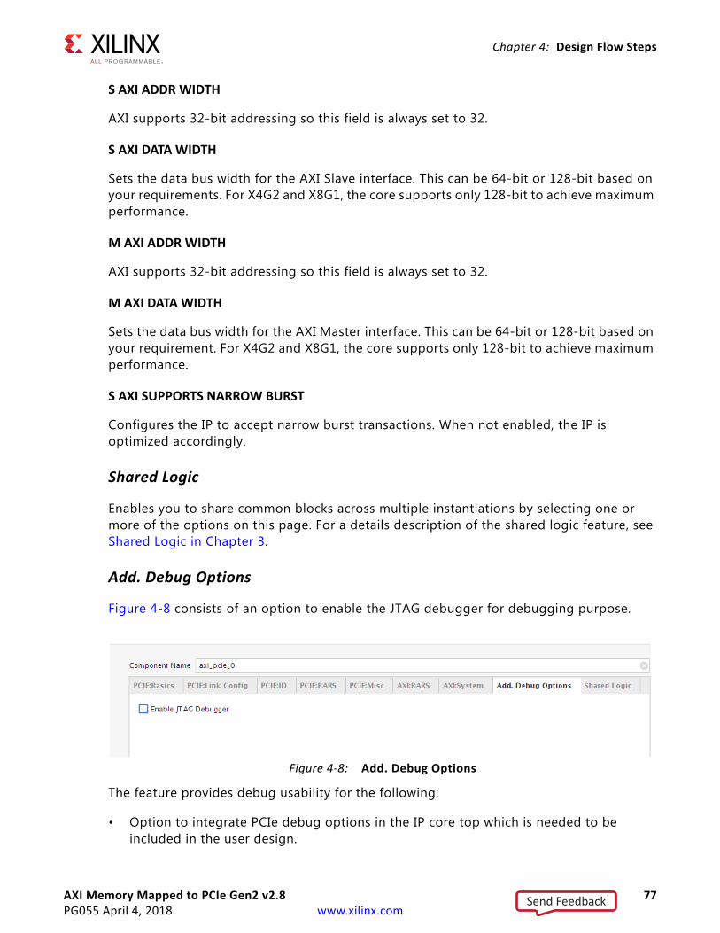
AXI Memory Mapped to PCIe Gen2 v2.8 77PG055 April 4, 2018 www.xilinx.com
Chapter 4: Design Flow Steps
S AXI ADDR WIDTH
AXI supports 32-bit addressing so this field is always set to 32.
S AXI DATA WIDTH
Sets the data bus width for the AXI Slave interface. This can be 64-bit or 128-bit based on your requirements. For X4G2 and X8G1, the core supports only 128-bit to achieve maximum performance.
M AXI ADDR WIDTH
AXI supports 32-bit addressing so this field is always set to 32.
M AXI DATA WIDTH
Sets the data bus width for the AXI Master interface. This can be 64-bit or 128-bit based on your requirement. For X4G2 and X8G1, the core supports only 128-bit to achieve maximum performance.
S AXI SUPPORTS NARROW BURST
Configures the IP to accept narrow burst transactions. When not enabled, the IP is optimized accordingly.
Shared Logic
Enables you to share common blocks across multiple instantiations by selecting one or more of the options on this page. For a details description of the shared logic feature, see Shared Logic in Chapter 3.
Add. Debug Options
Figure 4-8 consists of an option to enable the JTAG debugger for debugging purpose.
The feature provides debug usability for the following:
• Option to integrate PCIe debug options in the IP core top which is needed to be included in the user design.
X-Ref Target - Figure 4-8
Figure 4-8: Add. Debug Options
Send Feedback
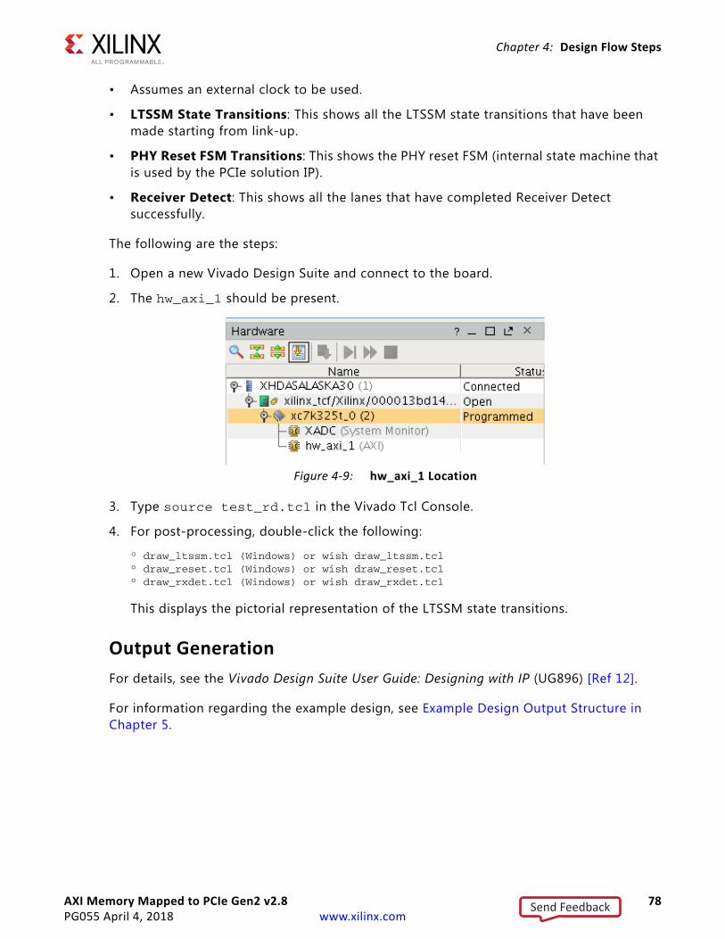
AXI Memory Mapped to PCIe Gen2 v2.8 78PG055 April 4, 2018 www.xilinx.com
Chapter 4: Design Flow Steps
• Assumes an external clock to be used.
• LTSSM State Transitions: This shows all the LTSSM state transitions that have been made starting from link-up.
• PHY Reset FSM Transitions: This shows the PHY reset FSM (internal state machine that is used by the PCIe solution IP).
• Receiver Detect: This shows all the lanes that have completed Receiver Detect successfully.
The following are the steps:
1. Open a new Vivado Design Suite and connect to the board.
2. The hw_axi_1 should be present.
3. Type source test_rd.tcl in the Vivado Tcl Console.
4. For post-processing, double-click the following:
° draw_ltssm.tcl (Windows) or wish draw_ltssm.tcl° draw_reset.tcl (Windows) or wish draw_reset.tcl° draw_rxdet.tcl (Windows) or wish draw_rxdet.tcl
This displays the pictorial representation of the LTSSM state transitions.
Output GenerationFor details, see the Vivado Design Suite User Guide: Designing with IP (UG896) [Ref 12].
For information regarding the example design, see Example Design Output Structure in Chapter 5.
X-Ref Target - Figure 4-9
Figure 4-9: hw_axi_1 Location
Send Feedback
AXI Memory Mapped to PCIe Gen2 v2.8 79PG055 April 4, 2018 www.xilinx.com
Chapter 4: Design Flow Steps
Constraining the CoreThis section contains information about constraining the core in the Vivado Design Suite.
Required ConstraintsThe AXI Memory Mapped to PCI Express core requires a clock period constraint for the REFCLK input that agrees with the C_REF_CLK_FREQ parameter setting. In addition, pin-placement (LOC) constraints are needed that are board/part/package specific.
See Placement Constraints for more details on the constraint paths for FPGA architectures.
Additional information on clocking can be found in the Xilinx Solution Center for PCI Express (see Solution Centers, page 95).
System IntegrationSome additional components to this system in the Vivado IP integrator can include the need to connect the MicroBlaze™ processor or Zynq® device ARM® processor peripheral to communicate with PCI Express (in addition to the AXI4-Lite register port on the PCIe bridge). The AXI Interconnect provides this capability and performs the necessarily conversions for the various AXI ports that might be connected to the AXI Interconnect IP (described in [Ref 9]).
The AXI Memory Mapped to PCI Express core can be configured with each port connection for an AXI Vivado IP integrator system topology. When instantiating the core, ensure the following bus interface tags are defined.
BUS_INTERFACE M_AXIBUS_INTERFACE S_AXIBUS_INTERFACE S_AXI_CTL
PCIe Clock Integration
The PCIe differential clock input in the system might need to use a differential input buffer (that is instantiated separately) from the AXI Memory Mapped to PCI Express core. The Vivado IP integrator automatically inserts the appropriate clock buffer.
Placement ConstraintsThe AXI Memory Mapped to PCI Express core provides a Xilinx design constraint (XDC) file for all supported PCIe, Part, and Package permutations. You can find the generated XDC file in the Sources tab of the Vivado IDE after generating the IP in the Customize IP dialog box.
Send Feedback
AXI Memory Mapped to PCIe Gen2 v2.8 80PG055 April 4, 2018 www.xilinx.com
Chapter 4: Design Flow Steps
For design platforms, it might be necessary to manually place and constrain the underlying blocks of the AXI Memory Mapped to PCI Express core. The modules to assign a LOC constraint include:
• the embedded integrated block for PCIe itself
• the GTX transceivers (for each channel)
• the PCIe differential clock input (if utilized)
The following subsection describes the example location constraints.
Location Constraints for Virtex-7 and Kintex-7 FPGAs
This section highlights the LOC constraints to be specified in the XDC file for the AXI Memory Mapped to PCI Express core for design implementations.
For placement/path information on the integrated block for PCIe itself, the following constraint can be utilized:
set_property LOC PCIE_X*Y* [get_cells {U0/comp_axi_enhanced_pcie/comp_enhanced_core_top_wrap/axi_pcie_enhanced_core_top_i/pcie_7x_v2_0_inst/pcie_top_i/pcie_7x_i/pcie_block_i}]
For placement/path information of the GTX transceivers, the following constraint can be utilized:
set_property LOC GTXE2_CHANNEL_X*Y* [get_cells {U0/comp_axi_enhanced_pcie/comp_enhanced_core_top_wrap/axi_pcie_enhanced_core_top_i/pcie_7x_v2_0_inst/gt_ges.gt_top_i/pipe_wrapper_i/pipe_lane[0].gt_wrapper_i/gtx_channel.gtxe2_channel_i}]
For placement/path constraints of the input PCIe differential clock source (using the example provided in System Integration), the following can be utilized:
set_property LOC IBUFDS_GTE2_X*Y* [get_cells {*/PCIe_Diff_Clk_I/USE_IBUFDS_GTE2.GEN_IBUFDS_GTE2[0].IBUFDS_GTE2_I}]
Location Constraints for Artix-7 FPGAs
Special consideration must be given to Artix®-7 device implementations. The same IP block constraint can be used as described previously (see Location Constraints for Virtex-7 and Kintex-7 FPGAs, page 80). However, the PCIe serial transceiver wrapper instance is different in the IP. Use the following LOC constraint for the GTP transceivers in Artix-7 devices.
set_property LOC GTPE2_CHANNEL_X*Y* [get_cells {U0/comp_axi_enhanced_pcie/comp_enhanced_core_top_wrap/axi_pcie_enhanced_core_top_i/pcie_7x_v2_0_inst/gt_ges.gt_top_i/pipe_wrapper_i/pipe_lane[0].gt_wrapper_i/gtp_channel.gtpe2_channel_i}]
Send Feedback

AXI Memory Mapped to PCIe Gen2 v2.8 81PG055 April 4, 2018 www.xilinx.com
Chapter 4: Design Flow Steps
Also for Artix-7 devices, the GTP_COMMON must be constrained to a location. The following LOC constraint can be utilized.
set_property LOC GTPE2_COMMON_X*Y* [get_cells {U0/comp_axi_enhanced_pcie/comp_enhanced_core_top_wrap/axi_pcie_enhanced_core_top_i/pcie_7x_v2_0_inst/gt_ges.gt_top_i/pipe_wrapper_i/pipe_lane[0].pipe_quad.pipe_common.qpll_wrapper_i/gtp_common.gtpe2_common_i}]
Clock FrequenciesThe AXI Memory Mapped to PCI Express Bridge supports reference clock frequencies of 100 MHz, and 250 MHz and is configurable within the Vivado IDE.
Clock ManagementFor details, see Clocking in Chapter 3.
Clock PlacementFor details, see Placement Constraints.
BankingThis section is not applicable for this IP core.
Transceiver PlacementThe Transceiver primitives adjacent to the PCIe hard block should be used to aid in the place and route of the solution IP. The adjacent Transceiver banks one above or one below the desired PCIe hard block can also be used. Transceivers outside this range are not likely to meet the timing requirements for the PCI Express Solution IP and should not be used.
Simulation• For comprehensive information about Vivado simulation components, as well as
information about using supported third party tools, see the Vivado Design Suite User Guide: Logic Simulation (UG900) [Ref 13].
• For information regarding simulating the example design, see Simulation Design Overview in Chapter 5.
IMPORTANT: For cores targeting 7 series or Zynq-7000 AP SoC devices, UNIFAST libraries are not supported. Xilinx IP is tested and qualified with UNISIM libraries only.
Send Feedback
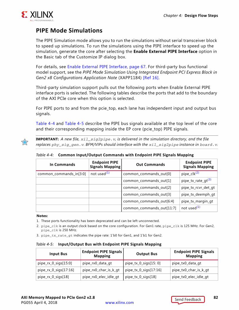
AXI Memory Mapped to PCIe Gen2 v2.8 82PG055 April 4, 2018 www.xilinx.com
Chapter 4: Design Flow Steps
PIPE Mode SimulationsThe PIPE Simulation mode allows you to run the simulations without serial transceiver block to speed up simulations. To run the simulations using the PIPE interface to speed up the simulation, generate the core after selecting the Enable External PIPE Interface option in the Basic tab of the Customize IP dialog box.
For details, see Enable External PIPE Interface, page 67. For third-party bus functional model support, see the PIPE Mode Simulation Using Integrated Endpoint PCI Express Block in Gen2 x8 Configurations Application Note (XAPP1184) [Ref 16].
Third-party simulation support pulls out the following ports when Enable External PIPE interface ports is selected. The following tables describe the ports that add to the boundary of the AXI PCIe core when this option is selected.
For PIPE ports to and from the pcie_top, each lane has independent input and output bus signals.
Table 4-4 and Table 4-5 describe the PIPE bus signals available at the top level of the core and their corresponding mapping inside the EP core (pcie_top) PIPE signals.
IMPORTANT: A new file, xil_sig2pipe.v, is delivered in the simulation directory, and the file replaces phy_sig_gen.v. BFM/VIPs should interface with the xil_sig2pipe instance in board.v.
Table 4-4: Common Input/Output Commands with Endpoint PIPE Signals Mapping
In Commands Endpoint PIPE Signals Mapping Out Commands Endpoint PIPE
Signals Mapping
common_commands_in[3:0] not used(1) common_commands_out[0] pipe_clk(2)
common_commands_out[1] pipe_tx_rate_gt(3)
common_commands_out[2] pipe_tx_rcvr_det_gt
common_commands_out[3] pipe_tx_deemph_gt
common_commands_out[6:4] pipe_tx_margin_gt
common_commands_out[11:7] not used(1)
Notes: 1. These ports functionality has been deprecated and can be left unconnected.2. pipe_clk is an output clock based on the core configuration. For Gen1 rate, pipe_clk is 125 MHz. For Gen2,
pipe_clk is 250 MHz.3. pipe_tx_rate_gt indicates the pipe rate: 1’b0 for Gen1, and 1’b1 for Gen2.
Table 4-5: Input/Output Bus with Endpoint PIPE Signals Mapping
Input Bus Endpoint PIPE Signals Mapping Output Bus Endpoint PIPE Signals
Mapping
pipe_rx_0_sigs[15:0] pipe_rx0_data_gt pipe_tx_0_sigs[15: 0] pipe_tx0_data_gt
pipe_rx_0_sigs[17:16] pipe_rx0_char_is_k_gt pipe_tx_0_sigs[17:16] pipe_tx0_char_is_k_gt
pipe_rx_0_sigs[18] pipe_rx0_elec_idle_gt pipe_tx_0_sigs[18] pipe_tx0_elec_idle_gt
Send Feedback
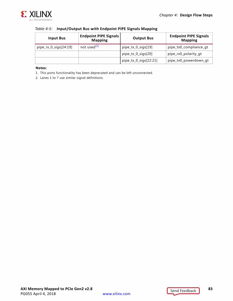
AXI Memory Mapped to PCIe Gen2 v2.8 83PG055 April 4, 2018 www.xilinx.com
Chapter 4: Design Flow Steps
pipe_rx_0_sigs[24:19] not used(1) pipe_tx_0_sigs[19] pipe_tx0_compliance_gt
pipe_tx_0_sigs[20] pipe_rx0_polarity_gt
pipe_tx_0_sigs[22:21] pipe_tx0_powerdown_gt
Notes: 1. This ports functionality has been deprecated and can be left unconnected.2. Lanes 1 to 7 use similar signal definitions.
Table 4-5: Input/Output Bus with Endpoint PIPE Signals Mapping
Input Bus Endpoint PIPE Signals Mapping Output Bus Endpoint PIPE Signals
Mapping
Send Feedback
AXI Memory Mapped to PCIe Gen2 v2.8 84PG055 April 4, 2018 www.xilinx.com
Chapter 5
Example DesignThis chapter contains information about the example design provided in the Vivado® Design Suite.
OverviewThe example simulation design for the Endpoint configuration of the AXI-PCIe block consists of two parts.
• Root Port Model: a test bench that generates, consumes, and checks PCI Express bus traffic
• AXI Block RAM Controller
Simulation Design OverviewFor the simulation design, transactions are sent from the Root Port Model to the AXI Memory Mapped to PCI Express core configured as an Endpoint and processed inside the AXI Block RAM controller design.
Figure 5-1 illustrates the simulation design provided with the AXI Memory Mapped to PCI Express core.
Send Feedback

AXI Memory Mapped to PCIe Gen2 v2.8 85PG055 April 4, 2018 www.xilinx.com
Chapter 5: Example Design
Note: The example design supports Verilog as the target language.
Customizing and Generating the Example DesignIn Customize IP dialog box, make the following selections for the example design.
1. In the PCIE:Basics page, the example design supports only an Endpoint (EP) device.
2. The PCIE:ID defaults are supported.
3. The PCIE:BARS defaults are supported.
4. The PCIE:Misc page defaults are supported.
5. In the AXI:BARS page, default values are assigned to the Base Address, High Address, and AXI to PCIe Translation values.
6. The AXI:System page default values are supported.
Note: After customizing the core, right-click the component name, and select Open IP Example Design. This opens a separate example design. Simulate the core by following the steps in the next section.
Simulating the Example DesignThe example design can be run in any configuration using:
• Vivado simulator
• Cadence IES Simulator
• Mentor Graphics Questa Advanced Simulator
• VCS Simulator
X-Ref Target - Figure 5-1
Figure 5-1: Example Design Block Diagram
X13767
TrafficGenerator DS Port AXI PCIe (EP)
AXI BRAMController
(inbuilt BRAM)
AXI4 InterfacePCIe Link
Send Feedback
AXI Memory Mapped to PCIe Gen2 v2.8 86PG055 April 4, 2018 www.xilinx.com
Chapter 5: Example Design
Vivado Simulator
By defaults, the simulator is set to Vivado simulator. To run a simulation, click Run Behavioral Simulation in the Flow Navigator.
Cadence IES
For a Cadence IES simulation, the following steps are required:
1. In Vivado IDE, change the simulation settings as follows:
° Target simulator: Incisive Enterprise Simulator (IES)
2. On the simulator tab, select Run Simulation > Run behavioral simulation.
Mentor Graphics Questa Advanced Simulator
For a Questa Advanced Simulator simulation, the following steps are required:
1. In the Vivado IDE, change the simulation settings as follows:
° Target simulator: Questa Advanced Simulator/ModelSim
2. On the Simulator tab, select Run Simulation > Run behavioral simulation.
VCS Simulator
For a VCS simulation, the following steps are required:
1. In Vivado IDE, change the simulation settings as follows:
° Target simulator: Verilog Compiler Simulator (VCS)
2. On the simulator tab, select Run Simulation > Run behavioral simulation.
IMPORTANT: Simulation is not supported for configurations with the Silicon Revision option set to IES. Only implementation is supported.
Implementation Design OverviewFor implementation design, the AXI Block RAM controller can be used as a scratch pad memory to write and read to Block RAM locations.
Send Feedback
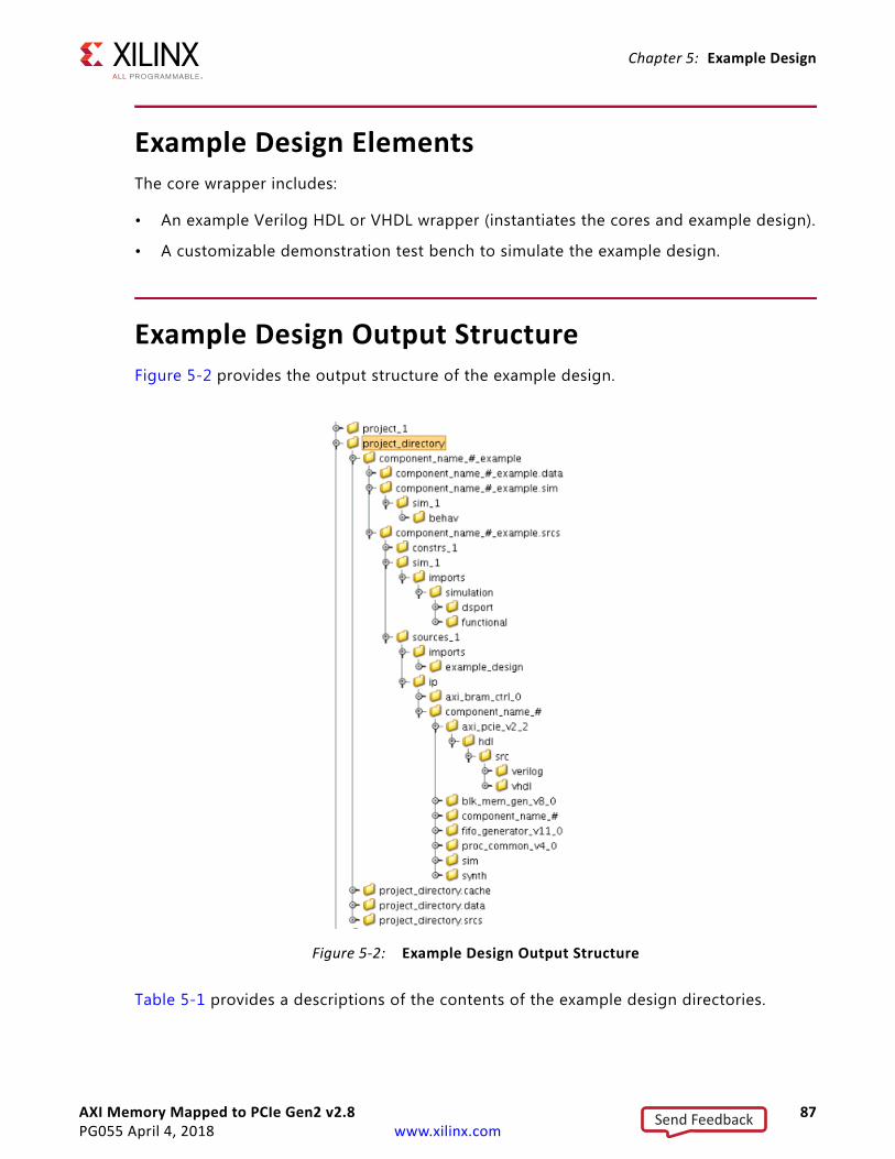
AXI Memory Mapped to PCIe Gen2 v2.8 87PG055 April 4, 2018 www.xilinx.com
Chapter 5: Example Design
Example Design ElementsThe core wrapper includes:
• An example Verilog HDL or VHDL wrapper (instantiates the cores and example design).
• A customizable demonstration test bench to simulate the example design.
Example Design Output StructureFigure 5-2 provides the output structure of the example design.
Table 5-1 provides a descriptions of the contents of the example design directories.
X-Ref Target - Figure 5-2
Figure 5-2: Example Design Output Structure
Send Feedback
AXI Memory Mapped to PCIe Gen2 v2.8 88PG055 April 4, 2018 www.xilinx.com
Chapter 5: Example Design
Table 5-1: Example Design StructureDirectory Description
project_1/axi_pcie_0_example Contains all example design files.
project_1/axi_pcie_0_example/axi_pcie_0_example.srcs/sources_1/imports/example_design/
Contains the top module for the example design, xilinx_axi_pcie_ep.v.
project_1/axi_pcie_0_example/axi_pcie_0_example.srcs/sources_1/ip/axi_pcie_0
Contains the XDC file based on device selected, all design files and subcores used in axi_pcie, and the top modules for simulation and synthesis.
project_1/axi_pcie_0_example/axi_pcie_0_example.srcs/sources_1/ip/axi_bram_ctrl_0
Contains block RAM controller files used in example design.
project_1/axi_pcie_0_example/axi_pcie_0_example.srcs/sim_1/imports/simulation/dsport
Contains all RP files, cgator and PIO files.
project_1/axi_pcie_0_example/axi_pcie_0_example.srcs/sim_1/imports/simulation/functional
Contains the test bench file.
project_1/axi_pcie_0_example/axi_pcie_0_example.srcs/constrs_1/imports/example_design
Contains the example design XDC file.
Send Feedback
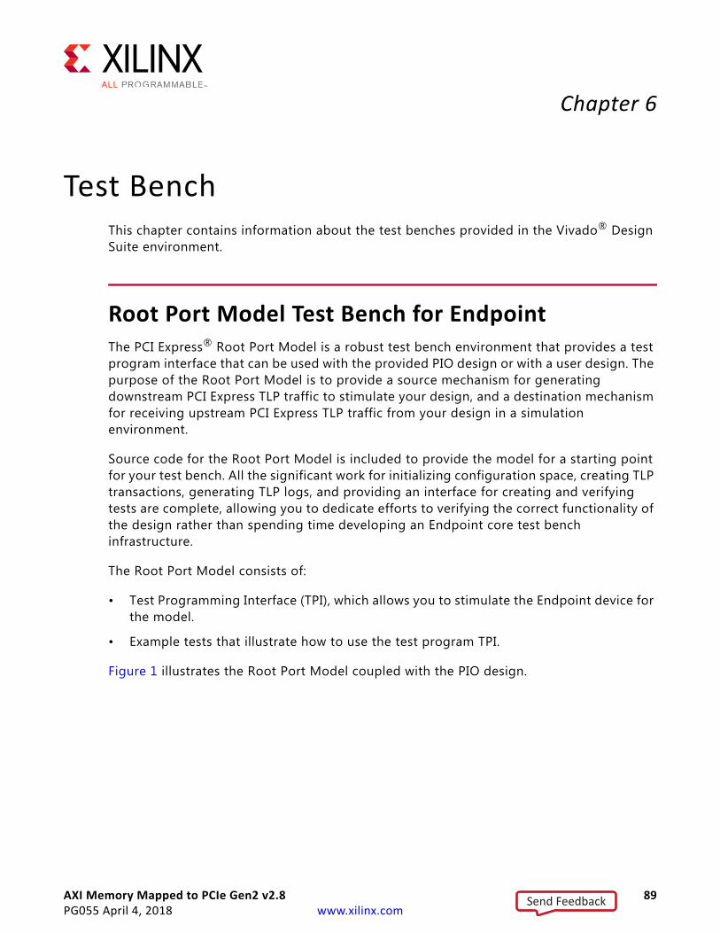
AXI Memory Mapped to PCIe Gen2 v2.8 89PG055 April 4, 2018 www.xilinx.com
Chapter 6
Test BenchThis chapter contains information about the test benches provided in the Vivado® Design Suite environment.
Root Port Model Test Bench for EndpointThe PCI Express® Root Port Model is a robust test bench environment that provides a test program interface that can be used with the provided PIO design or with a user design. The purpose of the Root Port Model is to provide a source mechanism for generating downstream PCI Express TLP traffic to stimulate your design, and a destination mechanism for receiving upstream PCI Express TLP traffic from your design in a simulation environment.
Source code for the Root Port Model is included to provide the model for a starting point for your test bench. All the significant work for initializing configuration space, creating TLP transactions, generating TLP logs, and providing an interface for creating and verifying tests are complete, allowing you to dedicate efforts to verifying the correct functionality of the design rather than spending time developing an Endpoint core test bench infrastructure.
The Root Port Model consists of:
• Test Programming Interface (TPI), which allows you to stimulate the Endpoint device for the model.
• Example tests that illustrate how to use the test program TPI.
Figure 1 illustrates the Root Port Model coupled with the PIO design.
Send Feedback
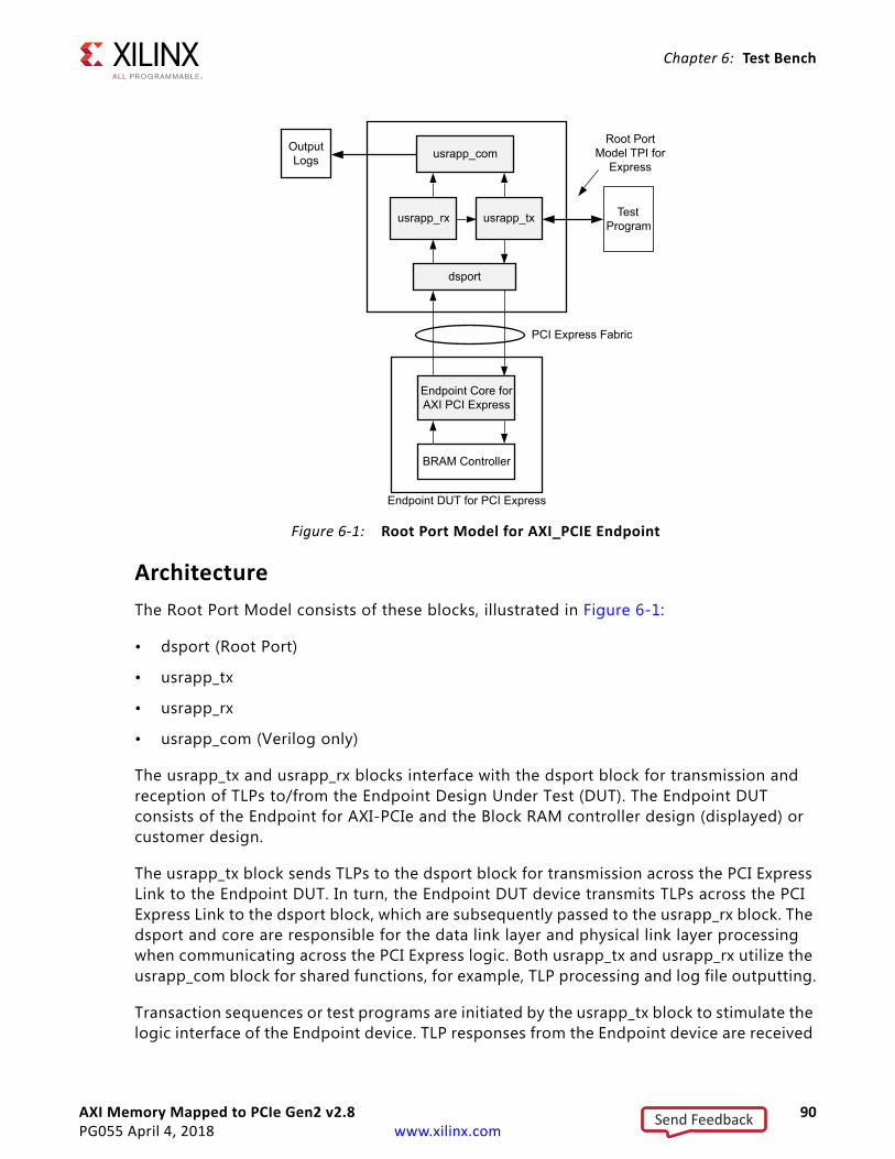
AXI Memory Mapped to PCIe Gen2 v2.8 90PG055 April 4, 2018 www.xilinx.com
Chapter 6: Test Bench
ArchitectureThe Root Port Model consists of these blocks, illustrated in Figure 6-1:
• dsport (Root Port)
• usrapp_tx
• usrapp_rx
• usrapp_com (Verilog only)
The usrapp_tx and usrapp_rx blocks interface with the dsport block for transmission and reception of TLPs to/from the Endpoint Design Under Test (DUT). The Endpoint DUT consists of the Endpoint for AXI-PCIe and the Block RAM controller design (displayed) or customer design.
The usrapp_tx block sends TLPs to the dsport block for transmission across the PCI Express Link to the Endpoint DUT. In turn, the Endpoint DUT device transmits TLPs across the PCI Express Link to the dsport block, which are subsequently passed to the usrapp_rx block. The dsport and core are responsible for the data link layer and physical link layer processing when communicating across the PCI Express logic. Both usrapp_tx and usrapp_rx utilize the usrapp_com block for shared functions, for example, TLP processing and log file outputting.
Transaction sequences or test programs are initiated by the usrapp_tx block to stimulate the logic interface of the Endpoint device. TLP responses from the Endpoint device are received
X-Ref Target - Figure 6-1
Figure 6-1: Root Port Model for AXI_PCIE Endpoint
Test Program
Endpoint DUT for PCI Express
PCI Express Fabric
Endpoint Core for AXI PCI Express
BRAM Controller
dsport
usrapp_tx
usrapp_com
usrapp_rx
Output Logs
Root Port Model TPI for
Express
Send Feedback
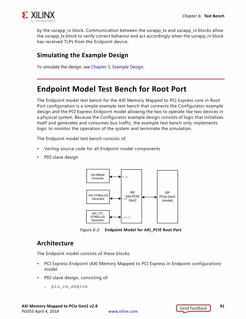
AXI Memory Mapped to PCIe Gen2 v2.8 91PG055 April 4, 2018 www.xilinx.com
Chapter 6: Test Bench
by the usrapp_rx block. Communication between the usrapp_tx and usrapp_rx blocks allow the usrapp_tx block to verify correct behavior and act accordingly when the usrapp_rx block has received TLPs from the Endpoint device.
Simulating the Example Design
To simulate the design, see Chapter 5, Example Design.
Endpoint Model Test Bench for Root PortThe Endpoint model test bench for the AXI Memory Mapped to PCI Express core in Root Port configuration is a simple example test bench that connects the Configurator example design and the PCI Express Endpoint model allowing the two to operate like two devices in a physical system. Because the Configurator example design consists of logic that initializes itself and generates and consumes bus traffic, the example test bench only implements logic to monitor the operation of the system and terminate the simulation.
The Endpoint model test bench consists of:
• Verilog source code for all Endpoint model components
• PIO slave design
ArchitectureThe Endpoint model consists of these blocks:
• PCI Express Endpoint (AXI Memory Mapped to PCI Express in Endpoint configuration) model.
• PIO slave design, consisting of:
° pio_rx_engine
X-Ref Target - Figure 6-2
Figure 6-2: Endpoint Model for AXI_PCIE Root Port
EP PCIe Gen2
(model)
RP AXI-PCIE
Gen2
AXI BRAM Controller
AXI STIMULUSGenerator
AXI_CTLSTIMULUSGenerator
m_axi
s_axi
s_axi_ctl
Send Feedback
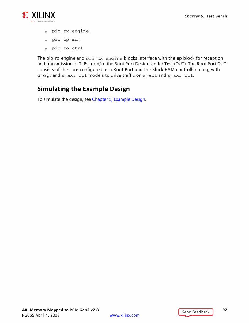
AXI Memory Mapped to PCIe Gen2 v2.8 92PG055 April 4, 2018 www.xilinx.com
Chapter 6: Test Bench
° pio_tx_engine
° pio_ep_mem
° pio_to_ctrl
The pio_rx_engine and pio_tx_engine blocks interface with the ep block for reception and transmission of TLPs from/to the Root Port Design Under Test (DUT). The Root Port DUT consists of the core configured as a Root Port and the Block RAM controller along with σ_αξι and s_axi_ctl models to drive traffic on s_axi and s_axi_ctl.
Simulating the Example DesignTo simulate the design, see Chapter 5, Example Design.
Send Feedback
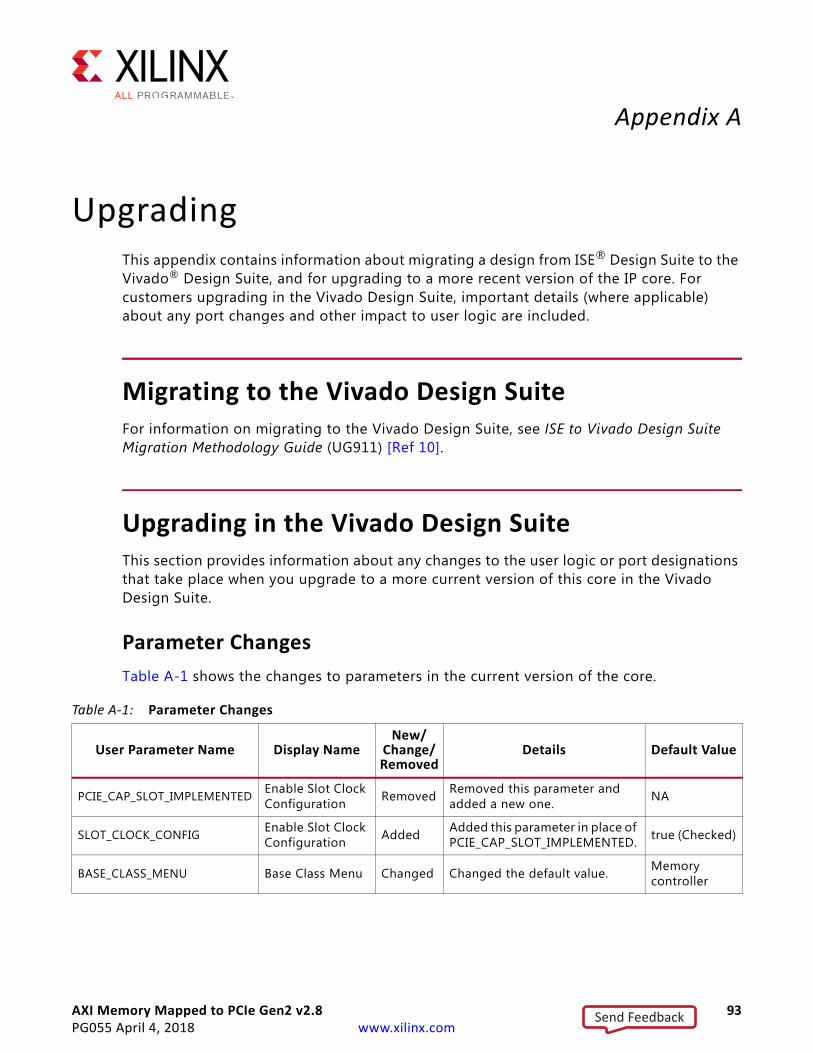
AXI Memory Mapped to PCIe Gen2 v2.8 93PG055 April 4, 2018 www.xilinx.com
Appendix A
UpgradingThis appendix contains information about migrating a design from ISE® Design Suite to the Vivado® Design Suite, and for upgrading to a more recent version of the IP core. For customers upgrading in the Vivado Design Suite, important details (where applicable) about any port changes and other impact to user logic are included.
Migrating to the Vivado Design SuiteFor information on migrating to the Vivado Design Suite, see ISE to Vivado Design Suite Migration Methodology Guide (UG911) [Ref 10].
Upgrading in the Vivado Design SuiteThis section provides information about any changes to the user logic or port designations that take place when you upgrade to a more current version of this core in the Vivado Design Suite.
Parameter ChangesTable A-1 shows the changes to parameters in the current version of the core.
Table A-1: Parameter Changes
User Parameter Name Display NameNew/
Change/Removed
Details Default Value
PCIE_CAP_SLOT_IMPLEMENTED Enable Slot Clock Configuration Removed Removed this parameter and
added a new one. NA
SLOT_CLOCK_CONFIG Enable Slot Clock Configuration Added Added this parameter in place of
PCIE_CAP_SLOT_IMPLEMENTED. true (Checked)
BASE_CLASS_MENU Base Class Menu Changed Changed the default value. Memory controller
Send Feedback
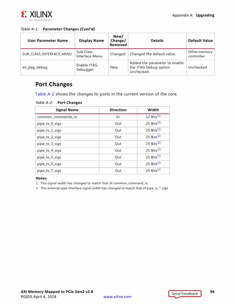
AXI Memory Mapped to PCIe Gen2 v2.8 94PG055 April 4, 2018 www.xilinx.com
Appendix A: Upgrading
Port ChangesTable A-2 shows the changes to ports in the current version of the core.
SUB_CLASS_INTERFACE_MENU Sub Class Interface Menu Changed Changed the default value. Other memory
controller
en_jtag_debug Enable JTAG Debugger New
Added the parameter to enable the JTAG Debug option Unchecked.
Unchecked
Table A-1: Parameter Changes (Cont’d)
User Parameter Name Display NameNew/
Change/Removed
Details Default Value
Table A-2: Port Changes
Signal Name Direction Width
common_commands_in In 12 Bits(1)
pipe_tx_0_sigs Out 25 Bits(2)
pipe_tx_1_sigs Out 25 Bits(2)
pipe_tx_2_sigs Out 25 Bits(2)
pipe_tx_3_sigs Out 25 Bits(2)
pipe_tx_4_sigs Out 25 Bits(2)
pipe_tx_5_sigs Out 25 Bits(2)
pipe_tx_6_sigs Out 25 Bits(2)
pipe_tx_7_sigs Out 25 Bits(2)
Notes: 1. This signal width has changed to match that of common_command_in.2. This external pipe interface signal width has changed to match that of pipe_rx_*_sigs.
Send Feedback
AXI Memory Mapped to PCIe Gen2 v2.8 95PG055 April 4, 2018 www.xilinx.com
Appendix B
DebuggingThis appendix provides information for using the resources available on the Xilinx® Support website, debug tools, and other step-by-step processes for debugging designs that use the AXI Memory Mapped to PCI Express core.
Finding Help on Xilinx.comTo help in the design and debug process when using the AXI Memory Mapped to PCI Express core, the Xilinx Support web page contains key resources such as product documentation, release notes, answer records, information about known issues, and links for opening a Technical Support WebCase.
DocumentationThis product guide is the main document associated with the AXI Memory Mapped to PCI Express core. This guide, along with documentation related to all products that aid in the design process, can be found on the Xilinx Support web page or by using the Xilinx Documentation Navigator.
You can download the Xilinx Documentation Navigator from the Downloads page. For more information about this tool and the features available, see the online help after installation.
Solution CentersSee the Xilinx Solution Centers for support on devices, software tools, and intellectual property at all stages of the design cycle. Topics include design assistance, advisories, and troubleshooting tips.
The PCI Express Solution Center is located at Xilinx Solution Center for PCI Express. Extensive debugging collateral is available in AR: 56802.
Answer RecordsAnswer Records include information about commonly encountered problems, helpful information on how to resolve these problems, and any known issues with a Xilinx product.
Send Feedback

AXI Memory Mapped to PCIe Gen2 v2.8 96PG055 April 4, 2018 www.xilinx.com
Appendix B: Debugging
Answer Records are created and maintained daily ensuring that users have access to the most accurate information available.
Answer Records for this core are listed below, and can be located by using the Search Support box on the main Xilinx support web page. To maximize your search results, use proper keywords, such as:
• the product name
• tool messages
• summary of the issue encountered
A filter search is available after results are returned to further target the results.
Master Answer Record for the AXI Memory Mapped to PCI Express
AR: 54646
Technical SupportXilinx provides technical support in the Xilinx Support web page for this LogiCORE™ IP product when used as described in the product documentation. Xilinx cannot guarantee timing, functionality, or support if you do any of the following:
• Implement the solution in devices that are not defined in the documentation.
• Customize the solution beyond that allowed in the product documentation.
• Change any section of the design labeled DO NOT MODIFY.
To contact Xilinx Technical Support, navigate to the Xilinx Support web page.
Debug ToolsThere are many tools available to address AXI Memory Mapped to PCI Express design issues. It is important to know which tools are useful for debugging various situations.
Vivado Design Suite Debug FeatureThe Vivado® Design Suite debug feature inserts logic analyzer and virtual I/O cores directly into your design. The debug feature also allows you to set trigger conditions to capture application and integrated block port signals in hardware. Captured signals can then be analyzed. This feature in the Vivado IDE is used for logic debugging and validation of a design running in Xilinx devices.
Send Feedback
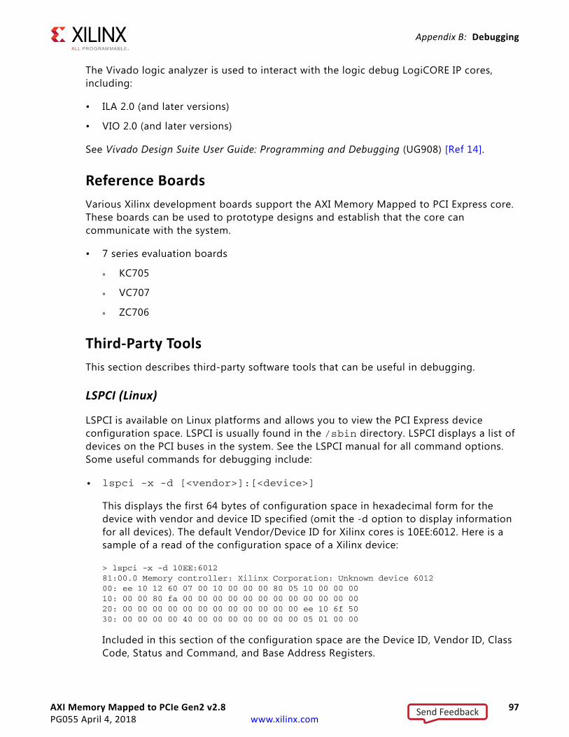
AXI Memory Mapped to PCIe Gen2 v2.8 97PG055 April 4, 2018 www.xilinx.com
Appendix B: Debugging
The Vivado logic analyzer is used to interact with the logic debug LogiCORE IP cores, including:
• ILA 2.0 (and later versions)
• VIO 2.0 (and later versions)
See Vivado Design Suite User Guide: Programming and Debugging (UG908) [Ref 14].
Reference BoardsVarious Xilinx development boards support the AXI Memory Mapped to PCI Express core. These boards can be used to prototype designs and establish that the core can communicate with the system.
• 7 series evaluation boards
° KC705
° VC707
° ZC706
Third-Party ToolsThis section describes third-party software tools that can be useful in debugging.
LSPCI (Linux)
LSPCI is available on Linux platforms and allows you to view the PCI Express device configuration space. LSPCI is usually found in the /sbin directory. LSPCI displays a list of devices on the PCI buses in the system. See the LSPCI manual for all command options. Some useful commands for debugging include:
• lspci -x -d [<vendor>]:[<device>]
This displays the first 64 bytes of configuration space in hexadecimal form for the device with vendor and device ID specified (omit the -d option to display information for all devices). The default Vendor/Device ID for Xilinx cores is 10EE:6012. Here is a sample of a read of the configuration space of a Xilinx device:
> lspci -x -d 10EE:601281:00.0 Memory controller: Xilinx Corporation: Unknown device 601200: ee 10 12 60 07 00 10 00 00 00 80 05 10 00 00 0010: 00 00 80 fa 00 00 00 00 00 00 00 00 00 00 00 0020: 00 00 00 00 00 00 00 00 00 00 00 00 ee 10 6f 5030: 00 00 00 00 40 00 00 00 00 00 00 00 05 01 00 00
Included in this section of the configuration space are the Device ID, Vendor ID, Class Code, Status and Command, and Base Address Registers.
Send Feedback
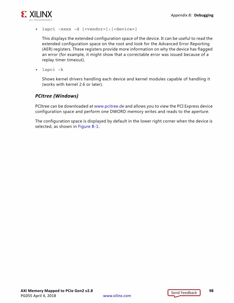
AXI Memory Mapped to PCIe Gen2 v2.8 98PG055 April 4, 2018 www.xilinx.com
Appendix B: Debugging
• lspci -xxxx -d [<vendor>]:[<device>]
This displays the extended configuration space of the device. It can be useful to read the extended configuration space on the root and look for the Advanced Error Reporting (AER) registers. These registers provide more information on why the device has flagged an error (for example, it might show that a correctable error was issued because of a replay timer timeout).
• lspci -k
Shows kernel drivers handling each device and kernel modules capable of handling it (works with kernel 2.6 or later).
PCItree (Windows)
PCItree can be downloaded at www.pcitree.de and allows you to view the PCI Express device configuration space and perform one DWORD memory writes and reads to the aperture.
The configuration space is displayed by default in the lower right corner when the device is selected, as shown in Figure B-1.
Send Feedback
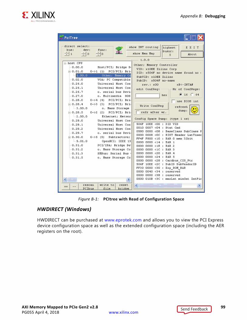
AXI Memory Mapped to PCIe Gen2 v2.8 99PG055 April 4, 2018 www.xilinx.com
Appendix B: Debugging
HWDIRECT (Windows)
HWDIRECT can be purchased at www.eprotek.com and allows you to view the PCI Express device configuration space as well as the extended configuration space (including the AER registers on the root).
X-Ref Target - Figure B-1
Figure B-1: PCItree with Read of Configuration Space
Send Feedback
AXI Memory Mapped to PCIe Gen2 v2.8 100PG055 April 4, 2018 www.xilinx.com
Appendix B: Debugging
PCI-SIG Software Suites
PCI-SIG® software suites such as PCIE-CV can be used to test compliance with the specification. This software can be downloaded at www.pcisig.com.
X-Ref Target - Figure B-2
Figure B-2: HWDIRECT with Read of Configuration Space
Send Feedback
AXI Memory Mapped to PCIe Gen2 v2.8 101PG055 April 4, 2018 www.xilinx.com
Appendix B: Debugging
Simulation DebugThe simulation debug flow for Mentor Graphics Questa Advanced Simulator is illustrated in Figure B-3. A similar approach can be used with other simulators.
Send Feedback

AXI Memory Mapped to PCIe Gen2 v2.8 102PG055 April 4, 2018 www.xilinx.com
Appendix B: Debugging
X-Ref Target - Figure B-3
Figure B-3: Questa Advanced Simulator Simulation Debug Flow
.
X13108
Update Questa Advanced Simulator to
version 6.4a or later.
Obtain a mixed-modesimulation license.
Need to compile and map the proper libraries. See the Vivado Design Suite User Guide: Logic
Simulation (UG900).
Add the “-L” switch with the appropriate library reference to the vslm command line. For example:
-L secureip or -L unisims_ver.
If the issue is more design specific, open a case with Xilinx Technical Support and include
a wlf file dump of the simulation. For best results, dump the entire
design hierarchy.
Questa Advanced Simulation Debug
Are you using Questa Advanced Simulator
version 6.4a or later?
If using VHDL, do you have a mixed-mode simulation license?
Do you get errors referring tofailing to access library?
Do you get errors indicating “PCIE_2_1” or other elements like
“BUFG” not defined?
Are you able to receive packets on the AXI RX interface
and transmit packets on the AXI TX interface?
Write to the PCI Command register at DWORD address offset
0x04 and set bits [2:0] to 111b
NoSecureIP models are used tosimulate the integrated blockfor PCI Express and the transceivers.To use these models, a VerilogLRM-IEEE 1364-2005 encription-compliant simulator is required.
A Verilog license is required tosimulate with the SecureIP models.If the user design uses VHDL, amixed-mode simulation license isrequired.
If the libraries are not compiled andmapped correctly, it causes errorssuch as:# ** Error: (vopt-19) Failed to access library 'secureip' at "secureip".# No such file or directory. (errno = ENOENT)# ** Error: ../../example_design/ xilinx_pcie_2_1_ep_7x.v(820): Library secureip not found.
To model the Integrated Block forPCI Express and the transceivers,theSecureIP models are used. These models must be referencedDuring the vsim call. Also, it is necessary to reference the unisims library and possibly xilinxcorelib Depending on the design.
One of the most common mistakes insimulation of an Endpoint is forgettingto set the Memory, I/O, and Bus MasterEnable bits to a 1 in the PCI Commandregister in the configuration space.
Yes
Yes
Yes
No
No
Yes
Yes
No
No
Send Feedback
AXI Memory Mapped to PCIe Gen2 v2.8 103PG055 April 4, 2018 www.xilinx.com
Appendix B: Debugging
Hardware DebugHardware issues can range from device recognition issues to problems seen after hours of testing. This section provides debug flow diagrams for some of the most common issues. Endpoints that are shaded gray indicate that more information is found in sections after Figure B-4.
Send Feedback

AXI Memory Mapped to PCIe Gen2 v2.8 104PG055 April 4, 2018 www.xilinx.com
Appendix B: Debugging
X-Ref Target - Figure B-4
Figure B-4: Design Fails in Hardware Debug Flow Diagram
Design Fails in Hardware
Does a soft reset fix the problem?(user_lnk_up = 1)
Is user_reset deasserted?(user_reset = 0)
Is user_lnk_up asserted?(user_lnk_up = 1)
To eliminate FPGA configuration as a root cause, perform a soft restart of the system. Performing asoft reset on the system will keeppower applied and forces re-enumeration of the device.
One reason user_reset stays asserted other than the systemreset being asserted is due to a faulty clock. This might keep thePLL from locking which holdsuser_reset asserted.
See “Link is Training Debug” section.
See "FPGA Configuration Time Debug" section.
Is it a multi-lane link?
Multi-lane links are susceptible to crosstalk and noise when all lanes are switching during training.A quick test for this is to force one lane operation, which can be done using an interposer or adapter to isolate the upper lanes, or using tape, such as Scotch tape, to tape off the upper lanes on the connector. For an embedded board, remove the AC capacitors to isolate the lanes.
Force x1 Operation
Does user_lnk_up = 1 when usingas x1 only?
There are potentially issues with the board layout causing interference when all lanes are switching. See
board debug suggestions.
Do you have a link analyzer?
Use the link analyzer to monitor the training sequence and to determine the point of failure.Have the analyzer
trigger on the first TS1 that it recognizes and then compare the output to the LTSSM state machine
sequences outlined in Chapter 4 of the PCI Express Base Specification.
The Vivado Design Suite debug feature can be used to determine the point of failure.
Using probes, an LED, Vivado Design Suite debug feature or some other method, determine ifuser_lnk_up is asserted. Whenuser_lnk_up is High, it indicates the core has achieved link up meaning the LTSSM is in L0 state and the data link layer is in the DL_Active state.
See "Clock Debug" section.
YesNo
No
Yes
Yes
No
No
Yes
Yes
No
Yes
X14216
Send Feedback
AXI Memory Mapped to PCIe Gen2 v2.8 105PG055 April 4, 2018 www.xilinx.com
Appendix B: Debugging
FPGA Configuration Time DebugDevice initialization and configuration issues can be caused by not having the FPGA configured fast enough to enter link training and be recognized by the system. Section 6.6 of PCI Express Base Specification, rev. 2.1 [Ref 8] states two rules that might be impacted by FPGA Configuration Time:
• A component must enter the LTSSM Detect state within 20 ms of the end of the Fundamental reset.
• A system must guarantee that all components intended to be software visible at boot time are ready to receive Configuration Requests within 100 ms of the end of Conventional Reset at the Root Complex.
These statements basically mean the FPGA must be configured within a certain finite time, and not meeting these requirements could cause problems with link training and device recognition.
Configuration can be accomplished using an onboard PROM or dynamically using JTAG. When using JTAG to configure the device, configuration typically occurs after the Chipset has enumerated each peripheral. After configuring the FPGA, a soft reset is required to restart enumeration and configuration of the device. A soft reset on a Windows-based PC is performed by going to Start > Shut Down and then selecting Restart.
To eliminate FPGA configuration as a root cause, you should perform a soft restart of the system. Performing a soft reset on the system keeps power applied and forces re-enumeration of the device. If the device links up and is recognized after a soft reset is performed, the FPGA configuration is most likely the issue. Most typical systems use ATX power supplies which provide some margin on this 100 ms window as the power supply is normally valid before the 100 ms window starts.
Link is Training DebugFigure B-5 shows the flowchart for link trained debug.
Send Feedback

AXI Memory Mapped to PCIe Gen2 v2.8 106PG055 April 4, 2018 www.xilinx.com
Appendix B: Debugging
X-Ref Target - Figure B-5
Figure B-5: Link Trained Debug Flow Diagram
.
X13110
See “Data Transfer Failing Debug” section
See “FPGA Configuration Time
Debug” section.
Compare the configuration register settings with the default example design.
If the default example design works, but mirroring the configuration parameters does not fix the
problem, then attention should be focused on the user application design.
Link is Training(user_lnk_up = 1)
Is the device recognized by the system? Can it be seen
by PCITREE (Windows) or Ispci (Linux)?
With no link analyzer, use the Vivado Design Suite debug feature
to gather the same information.
PCITREE and Ispci scan thesystem and display devicesrecognized during startup. Thesetools show the PCI configurationspace and its settings withinthe device.
To eliminate FPGA configuration as a root cause, perform a soft restart of the system, which keepspower applied and forces re-enumeration of the device.If this fixes the problem, the FPGA might not be configured in timefor the host to access the card.
The default example design is knownto work. Often, the default design works when a user design does not.This usually indicates some para-meter or resource conflict due to settings used for the user designconfiguration. Recommended: Mirror the defaultGUI settings in your design. Even though the design might notfunction, it should still be recognizedby the system.
Does a soft reset fix the problem?(user_lnk_up = 1)
Does the default example design fix the problem?
Do you have a link analyzer?
Does the default example design fix the problem?
It is likely the problem is due to the device not responding properly to some type of access. A link analyzer allows the user to view the link traffice and determine if something is incorrect. See the “Using
a Link Analyzer to Debug Device Recognition Issues” section.
Yes
No
No
Yes
Yes
No
Yes
Yes
No
No
Send Feedback
AXI Memory Mapped to PCIe Gen2 v2.8 107PG055 April 4, 2018 www.xilinx.com
Appendix B: Debugging
FPGA Configuration Time Debug
Device initialization and configuration issues can be caused by not having the FPGA configured fast enough to enter link training and be recognized by the system. Section 6.6 of PCI Express Base Specification, rev. 2.1 [Ref 8] states two rules that might be impacted by FPGA Configuration Time:
• A component must enter the LTSSM Detect state within 20 ms of the end of the Fundamental reset.
• A system must guarantee that all components intended to be software visible at boot time are ready to receive Configuration Requests within 100 ms of the end of Conventional Reset at the Root Complex.
These statements basically mean the FPGA must be configured within a certain finite time, and not meeting these requirements could cause problems with link training and device recognition.
Configuration can be accomplished using an onboard PROM or dynamically using JTAG. When using JTAG to configure the device, configuration typically occurs after the Chipset has enumerated each peripheral. After configuring the FPGA, a soft reset is required to restart enumeration and configuration of the device. A soft reset on a Windows based PC is performed by going to Start > Shut Down and then selecting Restart.
To eliminate FPGA configuration as a root cause, you should perform a soft restart of the system. Performing a soft reset on the system keeps power applied and forces re-enumeration of the device. If the device links up and is recognized after a soft reset is performed, then FPGA configuration is most likely the issue. Most typical systems use ATX power supplies which provides some margin on this 100 ms window as the power supply is normally valid before the 100 ms window starts.
Clock Debug
One reason to not deassert the user_reset_out signal is that the FPGA PLL (MMCM) and Transceiver PLL have not locked to the incoming clock. To verify lock, monitor the transceiver RXPLLLKDET output and the MMCM LOCK output. If the PLLs do not lock as expected, it is necessary to ensure the incoming reference clock meets the requirements in 7 Series FPGAs GTX/GTH Transceivers User Guide [Ref 3]. The REFCLK signal should be routed to the dedicated reference clock input pins on the serial transceiver, and the design should instantiate the IBUFDS_GTE2 primitive in the design. See the 7 Series FPGAs GTX/GTH Transceivers User Guide for more information on PCB layout requirements, including reference clock requirements.
Reference clock jitter can potentially close both the TX and RX eyes, depending on the frequency content of the phase jitter. Therefore, maintain as clean a reference clock as possible. Reduce crosstalk on REFCLK by isolating the clock signal from nearby high-speed traces. Maintain a separation of at least 25 mils from the nearest aggressor signals.
Send Feedback

AXI Memory Mapped to PCIe Gen2 v2.8 108PG055 April 4, 2018 www.xilinx.com
Appendix B: Debugging
The PCI Special Interest Group website provides other tools for ensuring the reference clocks are compliant to the requirements of the PCI Express Specification: www.pcisig.com/specifications/pciexpress/compliance/compliance_library.
Debugging PCI Configuration Space Parameters
Often, a user application fails to be recognized by the system, but the Xilinx PIO Example design works. In these cases, the user application is often using a PCI configuration space setting that is interfering with the system systems ability to recognize and allocate resources to the card.
The Xilinx solutions for PCI Express handle all configuration transactions internally and generate the correct responses to incoming configuration requests. Chipsets have limits to the amount of system resources they can allocate and the core must be configured to adhere to these limitations.
The resources requested by the Endpoint are identified by the BAR settings within the Endpoint configuration space. You should verify that the resources requested in each BAR can be allocated by the chipset. Generate a core that implements a small amount of memory (approximately 2 KB) to identify if this is the root cause.
The Class Code setting selected in the Vivado IDE can also affect configuration. The Class Code informs the Chipset as to what type of device the Endpoint is. Chipsets might expect a certain type of device to be plugged into the PCI Express slot and configuration might fail if it reads an unexpected Class Code. The BIOS could be configurable to work around this issue.
Using a link analyzer, it is possible to monitor the link traffic and possibly determine when during the enumeration and configuration process problems occur.
Using a Link Analyzer to Debug Device Recognition Issues
In cases where the link is up (user_lnk_up = 1), but the device is not recognized by the system, a link analyzer can help solve the issue. It is likely the FPGA is not responding properly to some type of access. The link view can be used to analyze the traffic and see if anything looks out of place.
To focus on the issue, it might be necessary to try different triggers. Here are some trigger examples:
• Trigger on the first INIT_FC1 and/or UPDATE_FC in either direction. This allows the analyzer to begin capture after link up.
• The first TLP normally transmitted to an Endpoint is the Set Slot Power Limit Message. This usually occurs before Configuration traffic begins. This might be a good trigger point.
• Trigger on Configuration TLPs.
Send Feedback
AXI Memory Mapped to PCIe Gen2 v2.8 109PG055 April 4, 2018 www.xilinx.com
Appendix B: Debugging
• Trigger on Memory Read or Memory Write TLPs.
Data Transfer Failing DebugFigure B-6 shows the flowchart for data transfer debug.
Send Feedback
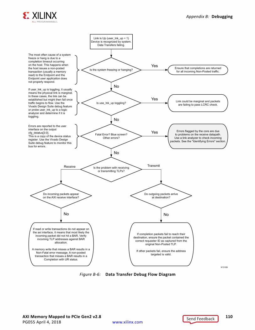
AXI Memory Mapped to PCIe Gen2 v2.8 110PG055 April 4, 2018 www.xilinx.com
Appendix B: Debugging
X-Ref Target - Figure B-6
Figure B-6: Data Transfer Debug Flow Diagram
Link is Up (user_lnk_up = 1)Device is recognized by system.
Data Transfers failing.
Is the system freezing or hanging?
Is use_lnk_up toggling? Link could be marginal and packetsare failing to pass LCRC check.
Fatal Error? Blue screen?Other errors?
Is the problem with receivingor transmitting TLPs?
The most often cause of a systemfreeze or hang is due to acompletion timeout occurring on the host. This happens whenthe host issues a non-postedtransaction (usually a memoryread) to the Endpoint and the Endpoint user application doesnot properly respond.
If user_lnk_up is toggling, it usuallymeans the physical link is marginal. In these cases, the link can be established but might then fail oncetraffic begins to flow. Use the Vivado Design Suite debug featureor probe user_lnk_up to a logic analyzer and determine if it is toggling.
If read or write transactions do not appear on the axi interface, it means that most likely the
incoming packet did not hit a BAR. Verify incoming TLP addresses against BAR
allocation.
A memory write that misses a BAR results in a Non-Fatal error message. A non-posted
transaction that misses a BAR results in a Completion with UR status.
Ensure that completions are returnedfor all incoming Non-Posted traffic.
Do incoming packets appearon the AXI receive interface?
Errors flagged by the core are dueto problems on the receive datapath.Use a link analyzer to check incoming
packets. See the "Identifying Errors" section.
Errors are reported to the userinterface on the output cfg_dstatus[3:0].This is a copy of the device statusregister. Use the Vivado Design Suite debug feature to monitor this bus for errors.
Do outgoing packets arriveat destination?
Receive Transmit
X13109
If completion packets fail to reach their destination, ensure the packet contained the
correct requester ID as captured from the original Non-Posted TLP.
If other packets fail, ensure the address targeted is valid.
No No
No
No
No
Yes
Yes
Yes
Send Feedback

AXI Memory Mapped to PCIe Gen2 v2.8 111PG055 April 4, 2018 www.xilinx.com
Appendix B: Debugging
Identifying ErrorsSee Abnormal Conditions in Chapter 3 for information about how the Slave side and Master side of the AXI Memory Mapped to PCI Express handle abnormal conditions.
Next StepsIf the debug suggestions listed previously do not resolve the issue, open a support case or visit the Xilinx User Community forums to have the appropriate Xilinx expert assist with the issue.
To can create a technical support case, go to the Xilinx Service Portal, and include the following items when opening a case:
° Detailed description of the issue and results of the steps listed above.
° Vivado Design Suite debug feature captures taken in the steps above.
To discuss possible solutions, use the Xilinx User Community Forums page.
Transceiver DebugTable B-1 describes the ports used to debug transceiver related issues.
IMPORTANT: Debugging transceiver issues is recommended for advanced users only.
Table B-1: Ports Used for Transceiver Debug
Port Direction Width Description
pipe_txprbssel I 3 PRBS input.
pipe_rxprbssel I 3 PRBS input.
pipe_rxprbsforceerr I 1 PRBS input.
pipe_rxprbscntrreset I 1 PRBS input.
pipe_loopback I 1 PIPE loopback.
pipe_rxprbserr O 1 PRBS output.
pipe_rst_fsm O Should be examined if pipe_rst_idle is stuck at 0.
pipe_qrst_fsm O Should be examined if pipe_rst_idle is stuck at 0.
pipe_sync_fsm_tx OShould be examined if pipe_rst_fsm stuck at 11'b10000000000, or pipe_rate_fsm stuck at 24'b000100000000000000000000.
pipe_sync_fsm_rx O Deprecated.
pipe_drp_fsm O Should be examined if pipe_rate_fsm is stuck at 100000000.
Send Feedback
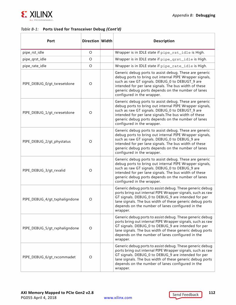
AXI Memory Mapped to PCIe Gen2 v2.8 112PG055 April 4, 2018 www.xilinx.com
Appendix B: Debugging
pipe_rst_idle O Wrapper is in IDLE state if pipe_rst_idle is High.
pipe_qrst_idle O Wrapper is in IDLE state if pipe_qrst_idle is High.
pipe_rate_idle O Wrapper is in IDLE state if pipe_rate_idle is High.
PIPE_DEBUG_0/gt_txresetdone O
Generic debug ports to assist debug. These are generic debug ports to bring out internal PIPE Wrapper signals, such as raw GT signals. DEBUG_0 to DEBUGT_9 are intended for per lane signals. The bus width of these generic debug ports depends on the number of lanes configured in the wrapper.
PIPE_DEBUG_1/gt_rxresetdone O
Generic debug ports to assist debug. These are generic debug ports to bring out internal PIPE Wrapper signals, such as raw GT signals. DEBUG_0 to DEBUGT_9 are intended for per lane signals.The bus width of these generic debug ports depends on the number of lanes configured in the wrapper.
PIPE_DEBUG_2/gt_phystatus O
Generic debug ports to assist debug. These are generic debug ports to bring out internal PIPE Wrapper signals, such as raw GT signals. DEBUG_0 to DEBUG_9 are intended for per lane signals. The bus width of these generic debug ports depends on the number of lanes configured in the wrapper.
PIPE_DEBUG_3/gt_rxvalid O
Generic debug ports to assist debug. These are generic debug ports to bring out internal PIPE Wrapper signals, such as raw GT signals. DEBUG_0 to DEBUG_9 are intended for per lane signals. The bus width of these generic debug ports depends on the number of lanes configured in the wrapper.
PIPE_DEBUG_4/gt_txphaligndone O
Generic debug ports to assist debug. These generic debug ports bring out internal PIPE Wrapper signals, such as raw GT signals. DEBUG_0 to DEBUG_9 are intended for per lane signals. The bus width of these generic debug ports depends on the number of lanes configured in the wrapper.
PIPE_DEBUG_5/gt_rxphaligndone O
Generic debug ports to assist debug. These generic debug ports bring out internal PIPE Wrapper signals, such as raw GT signals. DEBUG_0 to DEBUG_9 are intended for per lane signals. The bus width of these generic debug ports depends on the number of lanes configured in the wrapper.
PIPE_DEBUG_6/gt_rxcommadet O
Generic debug ports to assist debug. These generic debug ports bring out internal PIPE Wrapper signals, such as raw GT signals. DEBUG_0 to DEBUG_9 are intended for per lane signals. The bus width of these generic debug ports depends on the number of lanes configured in the wrapper.
Table B-1: Ports Used for Transceiver Debug (Cont’d)
Port Direction Width Description
Send Feedback
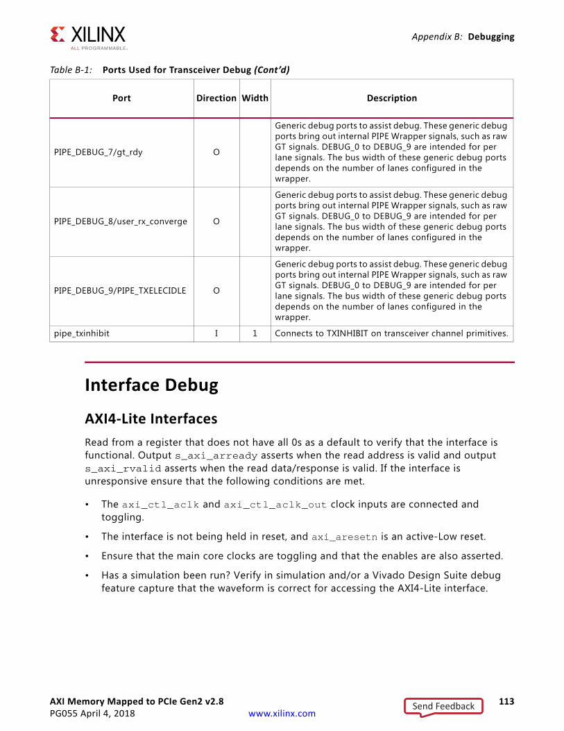
AXI Memory Mapped to PCIe Gen2 v2.8 113PG055 April 4, 2018 www.xilinx.com
Appendix B: Debugging
Interface Debug
AXI4-Lite InterfacesRead from a register that does not have all 0s as a default to verify that the interface is functional. Output s_axi_arready asserts when the read address is valid and output s_axi_rvalid asserts when the read data/response is valid. If the interface is unresponsive ensure that the following conditions are met.
• The axi_ctl_aclk and axi_ctl_aclk_out clock inputs are connected and toggling.
• The interface is not being held in reset, and axi_aresetn is an active-Low reset.
• Ensure that the main core clocks are toggling and that the enables are also asserted.
• Has a simulation been run? Verify in simulation and/or a Vivado Design Suite debug feature capture that the waveform is correct for accessing the AXI4-Lite interface.
PIPE_DEBUG_7/gt_rdy O
Generic debug ports to assist debug. These generic debug ports bring out internal PIPE Wrapper signals, such as raw GT signals. DEBUG_0 to DEBUG_9 are intended for per lane signals. The bus width of these generic debug ports depends on the number of lanes configured in the wrapper.
PIPE_DEBUG_8/user_rx_converge O
Generic debug ports to assist debug. These generic debug ports bring out internal PIPE Wrapper signals, such as raw GT signals. DEBUG_0 to DEBUG_9 are intended for per lane signals. The bus width of these generic debug ports depends on the number of lanes configured in the wrapper.
PIPE_DEBUG_9/PIPE_TXELECIDLE O
Generic debug ports to assist debug. These generic debug ports bring out internal PIPE Wrapper signals, such as raw GT signals. DEBUG_0 to DEBUG_9 are intended for per lane signals. The bus width of these generic debug ports depends on the number of lanes configured in the wrapper.
pipe_txinhibit I 1 Connects to TXINHIBIT on transceiver channel primitives.
Table B-1: Ports Used for Transceiver Debug (Cont’d)
Port Direction Width Description
Send Feedback
AXI Memory Mapped to PCIe Gen2 v2.8 114PG055 April 4, 2018 www.xilinx.com
Appendix C
Additional Resources and Legal Notices
Xilinx ResourcesFor support resources such as Answers, Documentation, Downloads, and Forums, see Xilinx Support.
Documentation Navigator and Design HubsXilinx® Documentation Navigator provides access to Xilinx documents, videos, and support resources, which you can filter and search to find information. To open the Xilinx Documentation Navigator (DocNav):
• From the Vivado® IDE, select Help > Documentation and Tutorials.
• On Windows, select Start > All Programs > Xilinx Design Tools > DocNav.
• At the Linux command prompt, enter docnav.
Xilinx Design Hubs provide links to documentation organized by design tasks and other topics, which you can use to learn key concepts and address frequently asked questions. To access the Design Hubs:
• In the Xilinx Documentation Navigator, click the Design Hubs View tab.
• On the Xilinx website, see the Design Hubs page.
Note: For more information on Documentation Navigator, see the Documentation Navigator page on the Xilinx website.
ReferencesThis section provides links to supplemental material useful to this document:
1. Vivado Design Suite AXI Reference Guide (UG1037)
2. 7 Series FPGAs Integrated Block for PCI Express LogiCORE IP Product Guide (PG054)
Send Feedback
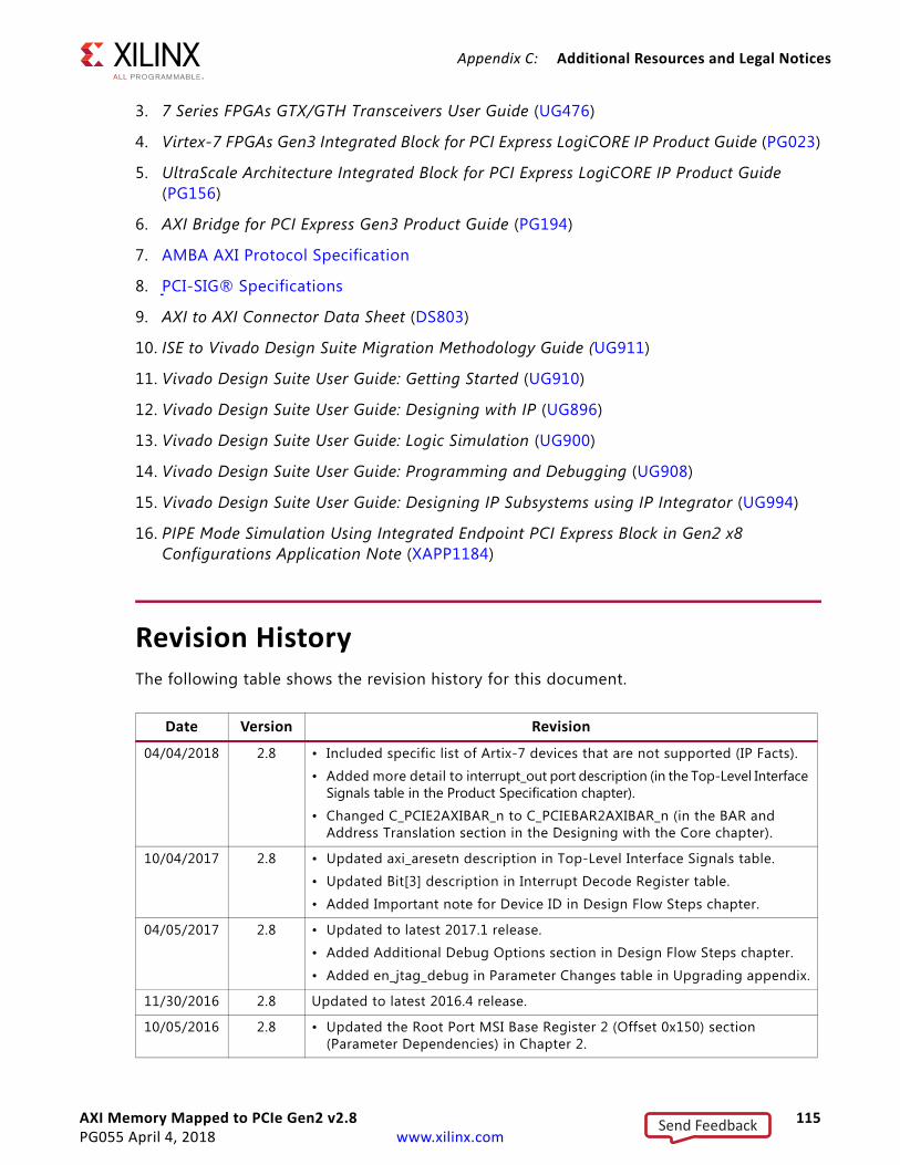
AXI Memory Mapped to PCIe Gen2 v2.8 115PG055 April 4, 2018 www.xilinx.com
Appendix C: Additional Resources and Legal Notices
3. 7 Series FPGAs GTX/GTH Transceivers User Guide (UG476)
4. Virtex-7 FPGAs Gen3 Integrated Block for PCI Express LogiCORE IP Product Guide (PG023)
5. UltraScale Architecture Integrated Block for PCI Express LogiCORE IP Product Guide (PG156)
6. AXI Bridge for PCI Express Gen3 Product Guide (PG194)
7. AMBA AXI Protocol Specification
8. PCI-SIG® Specifications
9. AXI to AXI Connector Data Sheet (DS803)
10. ISE to Vivado Design Suite Migration Methodology Guide (UG911)
11. Vivado Design Suite User Guide: Getting Started (UG910)
12. Vivado Design Suite User Guide: Designing with IP (UG896)
13. Vivado Design Suite User Guide: Logic Simulation (UG900)
14. Vivado Design Suite User Guide: Programming and Debugging (UG908)
15. Vivado Design Suite User Guide: Designing IP Subsystems using IP Integrator (UG994)
16. PIPE Mode Simulation Using Integrated Endpoint PCI Express Block in Gen2 x8 Configurations Application Note (XAPP1184)
Revision HistoryThe following table shows the revision history for this document.
Date Version Revision
04/04/2018 2.8 • Included specific list of Artix-7 devices that are not supported (IP Facts).
• Added more detail to interrupt_out port description (in the Top-Level Interface Signals table in the Product Specification chapter).
• Changed C_PCIE2AXIBAR_n to C_PCIEBAR2AXIBAR_n (in the BAR and Address Translation section in the Designing with the Core chapter).
10/04/2017 2.8 • Updated axi_aresetn description in Top-Level Interface Signals table.
• Updated Bit[3] description in Interrupt Decode Register table.
• Added Important note for Device ID in Design Flow Steps chapter.
04/05/2017 2.8 • Updated to latest 2017.1 release.
• Added Additional Debug Options section in Design Flow Steps chapter.
• Added en_jtag_debug in Parameter Changes table in Upgrading appendix.
11/30/2016 2.8 Updated to latest 2016.4 release.
10/05/2016 2.8 • Updated the Root Port MSI Base Register 2 (Offset 0x150) section (Parameter Dependencies) in Chapter 2.
Send Feedback
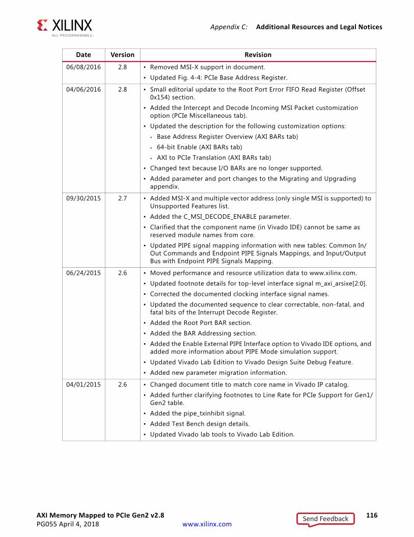
AXI Memory Mapped to PCIe Gen2 v2.8 116PG055 April 4, 2018 www.xilinx.com
Appendix C: Additional Resources and Legal Notices
06/08/2016 2.8 • Removed MSI-X support in document.
• Updated Fig. 4-4: PCIe Base Address Register.
04/06/2016 2.8 • Small editorial update to the Root Port Error FIFO Read Register (Offset 0x154) section.
• Added the Intercept and Decode Incoming MSI Packet customization option (PCIe Miscellaneous tab).
• Updated the description for the following customization options:
° Base Address Register Overview (AXI BARs tab)
° 64-bit Enable (AXI BARs tab)
° AXI to PCIe Translation (AXI BARs tab)
• Changed text because I/O BARs are no longer supported.
• Added parameter and port changes to the Migrating and Upgrading appendix.
09/30/2015 2.7 • Added MSI-X and multiple vector address (only single MSI is supported) to Unsupported Features list.
• Added the C_MSI_DECODE_ENABLE parameter.
• Clarified that the component name (in Vivado IDE) cannot be same as reserved module names from core.
• Updated PIPE signal mapping information with new tables: Common In/Out Commands and Endpoint PIPE Signals Mappings, and Input/Output Bus with Endpoint PIPE Signals Mapping.
06/24/2015 2.6 • Moved performance and resource utilization data to www.xilinx.com.
• Updated footnote details for top-level interface signal m_axi_arsixe[2:0].
• Corrected the documented clocking interface signal names.
• Updated the documented sequence to clear correctable, non-fatal, and fatal bits of the Interrupt Decode Register.
• Added the Root Port BAR section.
• Added the BAR Addressing section.
• Added the Enable External PIPE Interface option to Vivado IDE options, and added more information about PIPE Mode simulation support.
• Updated Vivado Lab Edition to Vivado Design Suite Debug Feature.
• Added new parameter migration information.
04/01/2015 2.6 • Changed document title to match core name in Vivado IP catalog.
• Added further clarifying footnotes to Line Rate for PCIe Support for Gen1/Gen2 table.
• Added the pipe_txinhibit signal.
• Added Test Bench design details.
• Updated Vivado lab tools to Vivado Lab Edition.
Date Version Revision
Send Feedback

AXI Memory Mapped to PCIe Gen2 v2.8 117PG055 April 4, 2018 www.xilinx.com
Appendix C: Additional Resources and Legal Notices
11/19/2014 2.5 • Correction made to 64-bit BAR size range upper limit.
• Updated the simulation procedures for Cadence Incisive Enterprise Simulator (IES), and Verilog Compiler Simulator (VCS).
• Added Important Note regarding the recommended version of Mentor Graphics Questa SIM to use to avoid simulation failure.
• Minor change made to debug diagrams.
10/01/2014 2.5 Updated for core v2.5.
06/02/2014 2.4 • Updated for core v2.4.
• Added new device support.
• Removed the axi_aclk and axi_ctl_aclk input ports.
04/02/2014 2.3 • Updated simulation information.
• Minor changes and updates.
12/18/2013 2.3 • Updated for core v2.3.
• Updated Example Design chapter.
• Updated parameter changes and port changes in Migrating and Updating chapter.
10/02/2013 2.2 • Updated for core v2.2.
• Updated resource utilization numbers.
• Added information about the Shared Logic feature.
• Added example design information.
• Added port and parameter upgrade information.
• Added transceiver debug information.
03/20/2013 2.0 Updated for core v2.0, and for Vivado Design Suite-only support.
12/18/2012 1.2 • Updated core v1.06a, ISE Design Suite 14.4, and Vivado Design Suite 2012.4.
• Updated Chapter 4, Customizing and Generating the Core.
• Added Appendix B, Debugging.
10/16/2012 1.1 • Updated core v1.05a, ISE Design Suite 14.3, and Vivado Design Suite 2012.3.
• Added Chapter 4, Customizing and Generating the Core.
• Major updates to PCIe Clock Integration.
• Added Unsupported Request to Upstream Traffic and Clock Frequencies.
07/25/2012 1.0 Initial Xilinx release. This release is for core version 1.04.a with ISE Design Suite 14.2 and Vivado Design Suite 2012.2. This document replaces DS820, LogiCORE IP AXI Bridge for PCI Express Data Sheet.
Date Version Revision
Send Feedback
AXI Memory Mapped to PCIe Gen2 v2.8 118PG055 April 4, 2018 www.xilinx.com
Appendix C: Additional Resources and Legal Notices
Please Read: Important Legal NoticesThe information disclosed to you hereunder (the "Materials") is provided solely for the selection and use of Xilinx products. To the maximum extent permitted by applicable law: (1) Materials are made available "AS IS" and with all faults, Xilinx hereby DISCLAIMS ALL WARRANTIES AND CONDITIONS, EXPRESS, IMPLIED, OR STATUTORY, INCLUDING BUT NOT LIMITED TO WARRANTIES OF MERCHANTABILITY, NON-INFRINGEMENT, OR FITNESS FOR ANY PARTICULAR PURPOSE; and (2) Xilinx shall not be liable (whether in contract or tort, including negligence, or under any other theory of liability) for any loss or damage of any kind or nature related to, arising under, or in connection with, the Materials (including your use of the Materials), including for any direct, indirect, special, incidental, or consequential loss or damage (including loss of data, profits, goodwill, or any type of loss or damage suffered as a result of any action brought by a third party) even if such damage or loss was reasonably foreseeable or Xilinx had been advised of the possibility of the same. Xilinx assumes no obligation to correct any errors contained in the Materials or to notify you of updates to the Materials or to product specifications. You may not reproduce, modify, distribute, or publicly display the Materials without prior written consent. Certain products are subject to the terms and conditions of Xilinx's limited warranty, please refer to Xilinx's Terms of Sale which can be viewed at https://www.xilinx.com/legal.htm#tos; IP cores may be subject to warranty and support terms contained in a license issued to you by Xilinx. Xilinx products are not designed or intended to be fail-safe or for use in any application requiring fail-safe performance; you assume sole risk and liability for use of Xilinx products in such critical applications, please refer to Xilinx's Terms of Sale which can be viewed at https://www.xilinx.com/legal.htm#tos.AUTOMOTIVE APPLICATIONS DISCLAIMERAUTOMOTIVE PRODUCTS (IDENTIFIED AS “XA” IN THE PART NUMBER) ARE NOT WARRANTED FOR USE IN THE DEPLOYMENT OF AIRBAGS OR FOR USE IN APPLICATIONS THAT AFFECT CONTROL OF A VEHICLE (“SAFETY APPLICATION”) UNLESS THERE IS A SAFETY CONCEPT OR REDUNDANCY FEATURE CONSISTENT WITH THE ISO 26262 AUTOMOTIVE SAFETY STANDARD (“SAFETY DESIGN”). CUSTOMER SHALL, PRIOR TO USING OR DISTRIBUTING ANY SYSTEMS THAT INCORPORATE PRODUCTS, THOROUGHLY TEST SUCH SYSTEMS FOR SAFETY PURPOSES. USE OF PRODUCTS IN A SAFETY APPLICATION WITHOUT A SAFETY DESIGN IS FULLY AT THE RISK OF CUSTOMER, SUBJECT ONLY TO APPLICABLE LAWS AND REGULATIONS GOVERNING LIMITATIONS ON PRODUCT LIABILITY.© Copyright 2012–2018 Xilinx, Inc. Xilinx, the Xilinx logo, Artix, ISE, Kintex, Spartan, Virtex, Vivado, Zynq, and other designated brands included herein are trademarks of Xilinx in the United States and other countries. AMBA, AMBA Designer, ARM, ARM1176JZ-S, CoreSight, Cortex, PrimeCell, and MPCore are trademarks of ARM in the EU and other countries. PCI, PCIe, and PCI Express are trademarks of PCI-SIG and used under license.All other trademarks are the property of their respective owners.
Send Feedback


![AXI Bridge for PCI Express v2 - Xilinx...The AXI Bridge for PCIe core is compliant with the ARM® AMBA® AXI4 Protocol Specification [Ref 7] and the PCI Express Base Specification](https://img.pdfslide.us/doc/110x75/5ea7f2aeb67dff456776491e/axi-bridge-for-pci-express-v2-xilinx-the-axi-bridge-for-pcie-core-is-compliant.jpg)