Embed Size (px)
DESCRIPTION
Gefran AVy Quick Setup
Citation preview
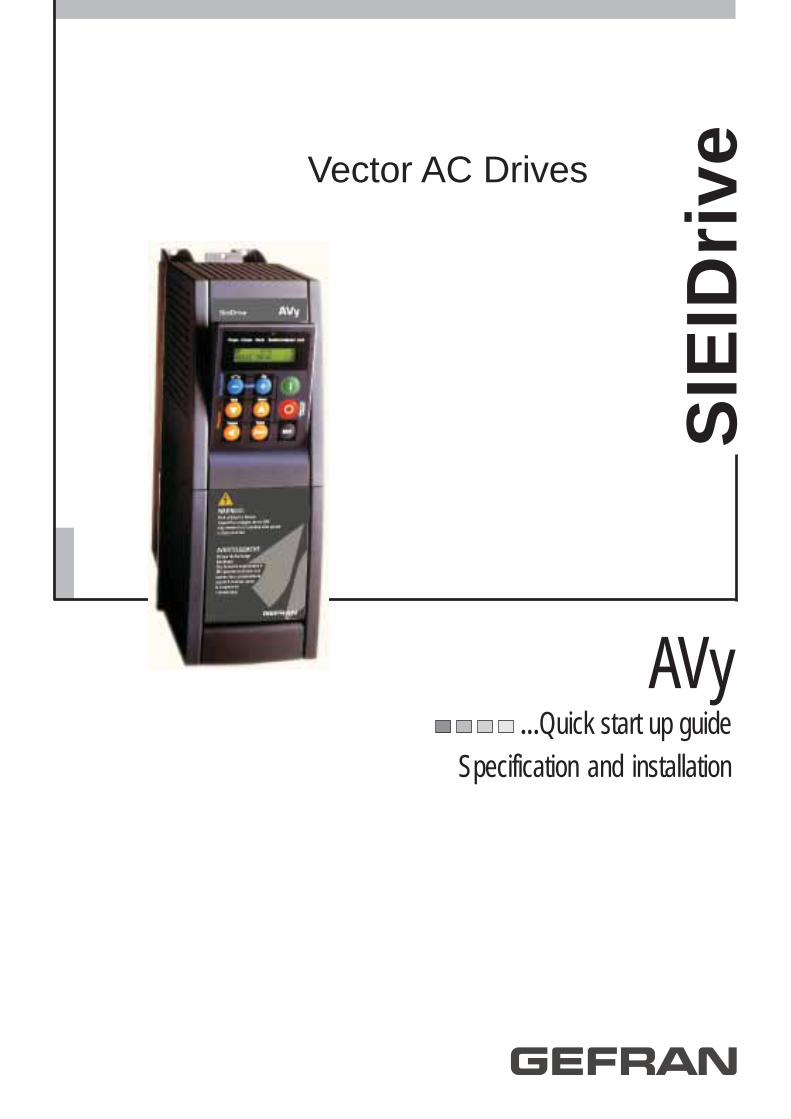
...Quick start up guideSpecification and installation
SIEI
Driv
eVector AC Drives
AVy
2
Thank you for choosing this Gefran product.We will be glad to receive any possible information which could help us improvingthis manual. The e-mail address is the following: [email protected].
Before using the product, read the safety instruction section carefully.
Keep the manual in a safe place and available to engineering and installation per-sonnel during the product functioning period.
Gefran S.p.A has the right to modify products, data and dimensions without notice.
The data can only be used for the product description and they can not be under-stood as legally stated properties.
All rights reserved
This manual is updated according the software version V1.X00.
Variation of the number replacing “X” have no influence on the functionality of thedevice.
The identification number of the software version can be read on the inverter name-plate or on the label on the FLASH memories mounted on the regulation card.

3
Table of ContentsSafety symbol legend ........................................................................................................................... 8
0. SAFETY PRECAUTIONS - PRECAUTIONS DE SECURITÉ ....................................... 9
1. QUICK START UP GUIDE ...................................................................................... 131.1. FUNCTIONAL CONNECTION DIAGRAM .................................................................................. 131.2. OVERVIEW .............................................................................................................................. 141.3. CONTROL TERMINALS............................................................................................................ 15
1.3.1 Maximum cable cross section for regulator terminals ....................................................... 161.4. POWER TERMINALS ............................................................................................................... 16
Figure 1.4.1: Power Terminals connection ................................................................................................ 161.4.1 Maximum cable cross section for power terminals ........................................................... 16
1.5 ENCODER TERMINALS (XE CONNECTOR) ................................................................................ 171.5.1 Encoder type connection .................................................................................................. 171.5.2 Jumpers setting ................................................................................................................ 181.5.3 Maximum cable length for encoder terminals ................................................................... 18
1.6. LIST OF JUMPERS AND DIP-SWITCH ..................................................................................... 191.7. KEYBOARD OPERATION .......................................................................................................... 20
1.7.1 LEDs & buttons ................................................................................................................. 201.7.2 Moving inside a menu ...................................................................................................... 22
1.8. PRE POWER CHECKS .............................................................................................................. 231.9. QUICK TUNING........................................................................................................................ 24
1.9.1 Motor Potentiometer .................................................................................................................. 27
1.10 OPTIONAL THINGS ................................................................................................................ 281.11 QUICK TUNING GUIDE FOR FACTORY CONFIGURED (OR PRE-CONFIGURED) DRIVES ........... 291.12 TROUBLESHOOTING .............................................................................................................. 30
Overflow list ....................................................................................................................................... 30LIST OF SELF TUNE ERROR MESSAGES.................................................................................... 31Failure alarms in the keypad display .......................................................................................... 32Other faults ............................................................................................................................... 34
2. FUNCTION AND FEATURE (OVERVIEW) .............................................................. 37
3. INSPECTION PROCEDURE, COMPONENT IDENTIFICATION AND STANDARDSPECIFICATION .................................................................................................... 393.1. UPON DELIVERY INSPECTION PROCEDURES .......................................................................... 39
3.1.1. General ........................................................................................................................... 393.1.2. Inverter type designation ................................................................................................ 393.1.3. Nameplate ...................................................................................................................... 40Figure 3.1.3.1: Identification nameplate .................................................................................................. 40Figure 3.1.3.2: Firmware & Card revision level nameplate ....................................................................... 40Figure 3.1.3.3: Nameplates position ......................................................................................................... 40
3.2. COMPONENT IDENTIFICATION .............................................................................................. 41Figure 3.2.1: Basic Setup of Frequency Inverter ...................................................................................... 41Figure 3.2.2: Drive view & components .................................................................................................... 42
4
3.3. STANDARD SPECIFICATIONS ................................................................................................. 433.3.1. Permissible environmental conditions .............................................................................. 43Table 3.3.1.1: Environmental specification ............................................................................................... 43
Disposal of the Device ........................................................................................................................ 443.3.2. AC Input/Output Connection ........................................................................................... 44Table 3.3.2.1:AC Input/Output specifications ............................................................................................ 453.3.3. AC Input current ............................................................................................................. 463.3.4. AC Output ........................................................................................................................ 46Table 3.3.3.1: Nominal Drive Current ....................................................................................................... 473.3.5. Open-Loop and Closed-Loop Control Section ................................................................... 483.3.6. Accuracy ......................................................................................................................... 49
4. INSTALLATION GUIDELINES ................................................................................ 514.1. MECHANICAL SPECIFICATION................................................................................................ 51
Figure 4.1.1: Drive dimensions (sizes 1007 ... 3150) ................................................................................ 51Figure 4.1.2: Mounting methods (sizes 1007 ... 3150) ............................................................................. 51Table 4.1.1: Drive dimensions and Weights (sizes 1007 ... 3150) ............................................................. 51Figure 4.1.3: Drive dimensions (sizes 4185 ... 82000) ............................................................................. 52Figure 4.1.4: Mounting methods (sizes 4185 ... 82000) ........................................................................... 52Table 4.1.2: Drive dimensions and Weights (sizes 4185 ... 82000) .......................................................... 52Figure 4.1.5: Keypad positioning .............................................................................................................. 53
4.2. WATTS LOSS, HEAT DISSIPATION, INTERNAL FANS AND MINIMUM CABINET OPENINGSUGGESTED FOR THE COOLING .................................................................................................... 53
Table 4.2.1: Heat dissipation and Required Air Flow ................................................................................ 53Table 4.2.2: Minimum cabinet opening suggested for the cooling ............................................................ 534.2.1 Cooling fans power supply ............................................................................................... 54Figure 4.2.1: UL type fans connections on AVy7900, AVy71100 and AVy71320 sizes .............................. 54Figure 4.2.2: UL type fans connections on AVy6750 and AVy82000 sizes ................................................ 54Figure 4.2.3: Example for external connection .......................................................................................... 54
4.3. INSTALLATION MOUNTING CLEARANCE ................................................................................ 55Figure 4.3.1: Max. Angle of Inclination ..................................................................................................... 55Figure 4.3.2: Mounting Clearance ............................................................................................................ 55
4.4. MOTORS AND ENCODERS ...................................................................................................... 564.4.1. Motors ............................................................................................................................ 564.4.2. Encoder ........................................................................................................................... 57Table 4.4.2.1: Recommended cable section and length for the connection of encoders ........................... 57Table 4.4.2.2: Encoders setting via S11...S23 jumpers ............................................................................. 58Table 4.4.2.3: Encoders connections ........................................................................................................ 58Table 4.4.2.4: Assignment of the high density XE connector for a sinusoidal or a digital encoder ............ 60
5. WIRING PROCEDURE ........................................................................................... 615.1. ACCESSING TO THE CONNECTORS ........................................................................................ 61
5.1.1 Removing the Covers ........................................................................................................ 61Figure 5.1.1: Removing the covers (sizes 1007 to 3150) .......................................................................... 61Figure 5.1.2: Removing the covers (sizes 4220 to 82000) ........................................................................ 62
5.2. POWER SECTION .................................................................................................................... 635.2.1. PV33-.. Power card ......................................................................................................... 63Figure 5.2.1.1: PV33-1-. power card (sizes 1007 to 1030) ....................................................................... 63Figure 5.2.1.2: PV33-2-.. power card (sizes 2040 to 2075) ...................................................................... 63Figure 5.2.1.3: PV33-3-.. power card (sizes 3110 and 3150) ................................................................... 64Figure 5.2.1.4: PV33-4-.. power card (sizes 4220 to 5550) ...................................................................... 64
5
Figure 5.2.1.5: PV33-5-.. power card (sizes 6750 to 71320) .................................................................... 65Figure 5.2.1.6: PV33-6-.. power card (sizes 81600 to 82000) .................................................................. 655.2.2. Terminal Assignment on Power section / Cable Cross-Section ......................................... 66Figure 5.2.2.1: Power Terminals connection ............................................................................................. 66Table 5.2.2.1: Maximum cable cross section for power terminals .......................................................... 66
5.3. REGULATION SECTION ........................................................................................................... 675.3.1 RV33 Regulation Card ...................................................................................................... 67Figure 5.3.1.1: RV33-4 Regulation Card Switch & Jumpers ..................................................................... 67Table 5.3.1.1: LEDs & Test points on Regulation card ............................................................................... 67Table 5.3.1.3: Jumpers on Regulation Card RV33-3 ................................................................................. 68Table 5.3.1.4: RV33 Regulation Card Switch S3 Settings ......................................................................... 685.3.2. Terminal Assignments on regulation section .................................................................... 69Table 5.3.2.1: Plug-in Terminal Strip Assignments .................................................................................... 69Table 5.3.2.2: Maximum permissible cable cross-section on the plug-in terminals of the regulator section ................................................................................................................................................................. 70
Table 5.3.2.3: Maximum Control Cable Lengths ....................................................................................... 70Figure 5.3.1.2: Potentials of the control section, Digital I/O NPN connection ........................................... 71
5.4. SERIAL INTERFACE ................................................................................................................. 725.4.1. Serial Interface Description ............................................................................................. 72Figure 5.4.1.1: RS485 Serial Interface ..................................................................................................... 725.4.2. RS 485 Serial Interface Connector Description ................................................................ 73Table 5.4.2.1: Assignment of the plug XS connector for the RS 485 serial interface ................................. 73
5.5. STANDARD CONNECTION DIAGRAM ..................................................................................... 745.5.1. AVy Connections ............................................................................................................. 74Figure 5.5.1.1:Control sequencing ............................................................................................................ 74Figure 5.5.1.2: Typical connection ............................................................................................................ 755.5.2. Parallel Connection on the AC (Input) and DC (Intermediate Circuit) Side of SeveralInverters .................................................................................................................................... 76Figure 5.5.2.1: Parallel Connection on the AC and DC Side of Several Inverters ...................................... 76
5.6. CIRCUIT PROTECTION ............................................................................................................. 775.6.1. External fuses of the power section ................................................................................. 77Table 5.6.1.1: External Fuse Types for AC input side ................................................................................ 775.6.2. External fuses of the power section DC input side ........................................................... 78Table 5.6.2.1: External fuses type for DC input side.................................................................................. 785.6.3. Internal fuses .................................................................................................................. 78Table 5.6.3.1: Internal fuses ..................................................................................................................... 78
5.7. CHOKES / FILTERS .................................................................................................................. 795.7.1. AC Input Chokes .............................................................................................................. 79Table 5.7.1.1:3-Phase AC Input Chokes .................................................................................................... 795.7.2. Output Chokes ................................................................................................................. 79Table 5.7.2.1: Recommended values for output chokes ............................................................................ 805.7.3. Interference Suppression Filters ...................................................................................... 80
5.8. BRAKING UNITS ..................................................................................................................... 81Figure 5.8.1: Operation with Braking Unit (Principle) ................................................................................ 815.8.1. Internal braking unit ........................................................................................................ 81Figure 5.8.1.1: Connection with internal Braking Unit and external braking resistor ................................. 815.8.2 External braking resistor ................................................................................................... 82Table 5.8.2.1: Lists and technical data of the external standard resistors for inverters AVy1007 to 5550 82Figure 5.8.2.2: Limit operating braking cycle with typical triangular power profile ................................... 82Figure 5.8.2.2: Braking cycle with TBR / TC = 20% ................................................................................. 83Figure 5.8.2.3:Generic braking cycle with triangular profile ..................................................................... 84
6
Table 5.8.2.2: Braking thresholds for different Mains .............................................................................. 85Table 5.8.2.3: Technical data of the internal braking units ........................................................................ 855.8.3. Calculation of generic external braking resistor to be combined with the internal brakingunit with an approximate method .............................................................................................. 86Figure 5.8.3.1: Power Resistor Overload Factor ....................................................................................... 86
5.9. BUFFERING THE REGULATOR SUPPLY .................................................................................... 87Table 5.9.1: DC Link Buffer Time ............................................................................................................. 87Figure 5.9.1: Buffering the Regulator Supply by Means of Additional Intermediate Circuit Capacitors ..... 87
5.10. AVY POWER DIP RIDE THROUGH DATA AND RESTART SETUP ............................................. 89Table 5.10.1: Drive Trip Times, 230-V Threshold ....................................................................................... 90Table 5.10.2: Drive Trip Times, 400-V Threshold ....................................................................................... 91Table 5.10.3: Drive Trip Time, 460-V Threshold ........................................................................................ 91
5.11. DISCHARGE TIME OF THE DC-LINK ....................................................................................... 92Table 5.11.1: DC Link Discharge Times .................................................................................................... 92
6. MAINTENANCE .................................................................................................... 936.1. CARE ...................................................................................................................................... 936.2. SERVICE .................................................................................................................................. 936.3. REPAIRS.................................................................................................................................. 936.4. CUSTOMER SERVICE .............................................................................................................. 93
Block diagram legend ................................................................................................................ 94
7. BLOCK DIAGRAM ................................................................................................. 95AVy Inverter Overview ........................................................................................................................ 95Digital inputs/Outputs & Mapping Standard and Option cards ............................................................. 96Analog Inputs/Outputs & Mapping ...................................................................................................... 97Speed Reference generation ............................................................................................................... 98Speed / Torque regulation ................................................................................................................... 99Ramp reference Block ....................................................................................................................... 100Speed regulator ................................................................................................................................. 101Speed regulator PI part ..................................................................................................................... 102Droop compensation ......................................................................................................................... 103Inertia / Loss compensation .............................................................................................................. 104Torque current regulator .................................................................................................................... 105Speed Feedback ............................................................................................................................... 106Motor control .................................................................................................................................... 107Motor parameters ............................................................................................................................. 108Sensorless parameters ..................................................................................................................... 109V/Hz functions ................................................................................................................................... 110Speed Threshold / Speed control ...................................................................................................... 111Speed adaptive and Speed zero logic ................................................................................................ 112PID function ...................................................................................................................................... 113Start and Stop management ............................................................................................................. 114Power loss stop control .................................................................................................................... 115Jog function ...................................................................................................................................... 116Motor potentiometer ......................................................................................................................... 117Multi speed ....................................................................................................................................... 118Dual Motor setup .............................................................................................................................. 119Brake unit function ............................................................................................................................ 120DC Braking function .......................................................................................................................... 121Dimension factor / Face value factor ................................................................................................. 122PAD parameters ................................................................................................................................ 123

7
Links function ................................................................................................................................... 124Test Generator .................................................................................................................................. 125Alarm mapping ................................................................................................................................. 126
8. PARAMETERS LIST ............................................................................................ 127
EMC DIRECTIVE ...................................................................................................... 154

8
Safety symbol legend
WARNING! Commands attention to an operating procedure, practice, condition, or statement which,if not strictly observed, could result in personai injury or death.
CAUTION! Commands attention to an operating procedure, practice, condition, or statement which,if not strictly observed, could result in damage or destruction of equipment.
The seriousness of the injuries and of the damages which could be caused by the non-observance of such indications, depends on the different conditions. Anyway, theinstructions given below should always be followed with the highest attention.
NOTE! Commands attention to an operating procedure, practice, condition, or statement thatmust be highlighted.
QS9—————— Quick Start up ——————
ATTENTION!
According to the EEC standards the AVy and accessoriesmust be used only after checking that the machine has beenproduced using those safety devices required by the 89/392/EEC set of rules, as far as the machine industry isconcerned.
Drive systems cause mechanical motion. It is theresponsibility of the user to insure that any such motiondoes not result in an unsafe condition. Factory providedinterlocks and operating limits should not be bypassed ormodified.
Selon les normes EEC, les drives AVy et leurs accessoiresdoivent être employés seulement après avoir verifié quela machine ait été produit avec les même dispositifs desécurité demandés par la réglementation 89/392/EECconcernant le secteur de l’industrie.
Les systèmes provoquent des mouvements mécaniques.L’utilisateur est responsable de la sécurité concernant lesmouvements mécaniques. Les dispositifs de sécuritéprévues par l’usine et les limitations operationelles nedoivent être dépassés ou modifiés.
WARNING - ELECTRICAL SHOCK AND BURN HAZARD /ATTENTION – DÉCHARGE ÉLECTRIQUE ET RISQUE DEBRÚLURE :
When using instruments such as oscilloscopes to work onlive equipment, the oscilloscope’s chassis should begrounded and a differential amplifier input should be used.Care should be used in the selection of probes and leadsand in the adjustment of the oscilloscope so that accuratereadings may be made. See instrument manufacturer’sinstruction book for proper operation and adjustments tothe instrument.
Lors de l’utilisation d’instruments (par exampleoscilloscope) sur des systémes en marche, le chassis del’oscilloscope doit être relié à la terre et un amplificateurdifférentiel devrait être utilisé en entrée.
Les sondes et conducteurs doivent être choissis avec soinpour effectuer les meilleures mesures à l’aide d’unoscilloscope.
Voir le manuel d’instruction pour une utilisation correctedes instruments.
WARNING - FIRE AND EXPLOSION HAZARD / ATTENTION– RISQUE D’INCENDIES ET D’EXPLOSIONS:
Fires or explosions might result from mounting Drives inhazardous areas such as locations where flammable orcombustible vapors or dusts are present. Drives should beinstalled away from hazardous areas, even if used withmotors suitable for use in these locations.
L’utilisation des drives dans des zônes à risques (présencede vapeurs ou de poussières inflammables), peut
provoquer des incendies ou des explosions. Les drivesdoivent être installés loin des zônes dangeureuses, etéquipés de moteurs appropriés.
WARNING - STRAIN HAZARD / ATTENTION ÀL’ÉLÉVATION:
Improper lifting practices can cause serious or fatal injury.Lift only with adequate equipment and trained personnel.
Une élévation inappropriée peut causer des dommagessérieux ou fatals. Il doit être élevé seulement avec desmoyens appropriés et par du personnel qualifié.
ATTENTION – CAS DE DECHARGE ELECTRIQUE:
Drives and motors must be ground connected accordingto the NEC.
Tous les moteurs et les drives doivent être mis à la terreselon le Code Electrique National ou équivalent.
WARNING / ATTENTION:
Replace all covers before applying power to the Drive.Failure to do so may result in death or serious injury.
Remettre tous les capots avant de mettre sous tension ledrive. Des erreurs peuvent provoquer de sérieux accidentsou même la mort.
WARNING / ATTENTION:
Adjustable frequency drives are electrical apparatus foruse in industrial installations. Parts of the Drives areenergized during operation. The electrical installation andthe opening of the device should therefore only be carriedout by qualified personnel. Improper installation of motorsor Drives may therefore cause the failure of the device aswell as serious injury to persons or material damage.
Drive is not equipped with motor overspeed protectionlogic.
Follow the instructions given in this manual and observethe local and national safety regulations applicable.
Les drives à fréquence variable sont des dispositifsélectriques utilisés dans des installations industriels. Unepartie des drives sont sous tension pendant l’operation.L’installation électrique et l’ouverture des drives devraitêtre executé uniquement par du personel qualifié. Demauvaises installations de moteurs ou de drives peuventprovoquer des dommages materiels ou blesser despersonnes. Le convertisseur n’est pas pourvu de protectioncontre vitesse de fuite du moteur.
On doit suivir les instructions donneés dans ce manuel etobserver les régles nationales de sécurité.
0. SAFETY PRECAUTIONS - PRECAUTIONS DE SECURITÉ
10QS AVy -HGB
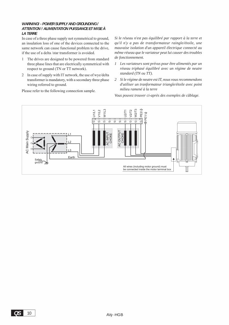
WARNING! - POWER SUPPLY AND GROUNDING /ATTENTION ! ALIMENTATION PUISSANCE ET MISE ÀLA TERREIn case of a three phase supply not symmetrical to ground,an insulation loss of one of the devices connected to thesame network can cause functional problem to the drive,if the use of a delta /star transformer is avoided.
1 The drives are designed to be powered from standardthree phase lines that are electrically symmetrical withrespect to ground (TN or TT network).
2 In case of supply with IT network, the use of wye/deltatransformer is mandatory, with a secondary three phasewiring referred to ground.
Please refer to the following connection sample.
Safetyground
L1
L2
L3
Earth
U1
/L1
V1
/L2
W1
/L3
U2
/T1
V2
/T2
W2
/T3
PE
2/
All wires (including motor ground) mustbe connected inside the motor terminal box
AC
OU
TP
UT
CH
OK
E
AC
Ma
inS
up
ply
AC
INP
UT
CH
OK
E
PE
1/
Si le réseau n'est pas équilibré par rapport à la terre etqu'il n'y a pas de transformateur raingle/étoile, unemauvaise isolation d'un appareil électrique connecté aumême réseau que le variateur peut lui causer des troublesde fonctionnement.
1 Les variateurs sont prévus pour être alimentés par unréseau triphasé équilibré avec un régime de neutrestandard (TN ou TT).
2 Si le régime de neutre est IT, nous vous recommendonsd'utiliser un tranformateur triangle/étoile avec pointmilieu ramené à la terre
Vous pouvez trouver ci-après des exemples de câblage.
QS11—————— Quick Start up ——————
CAUTION / PRECAUTION:
Do not connect power supply voltage that exceeds thestandard specification voltage fluctuation permissible. Ifexcessive voltage is applied to the Drive, damage to theinternal components will result.
Ne pas raccorder de tension d’alimentation dépassant lafluctuation de tension permise par les normes. Dans lecas d’ une alimentation en tension excessive, descomposants internes peuvent être endommagés.
CAUTION / PRECAUTION:
Do not operate the Drive without the ground wireconnected. The motor chassis should be grounded to earththrough a ground lead separate from all other equipmentground leads to prevent noise coupling.
The grounding connector shall be sized in accordance withthe NEC or Canadian Electrical Code. The connectionshall be made by a UL listed or CSA certified closed-loopterminal connector sized for the wire gauge involved. Theconnector is to be fixed using the crimp tool specified bythe connector manufacturer.
Ne pas faire fonctionner le drive sans prise de terre. Lechassis du moteur doit être mis à la terre à l’aide d’unconnecteur de terre separé des autres pour éviter le couplagedes perturbations. Le connecteur de terre devrait êtredimensionné selon la norme NEC ou le Canadian Electricalcode. Le raccordement devrait être fait par un connecteurcertifié et mentionné à boucle fermé par les normes CSA etUL et dimensionné pour l’épaisseur du cable correspondant.Le connecteur doit être fixé a l’aide d’un instrument deserrage specifié par le producteur du connecteur.
CAUTION / PRECAUTION:
Do not perform a megger test between the Drive terminalsor on the control circuit terminals.
Ne pas exécuter un test megger entre les bornes du driveou entre les bornes du circuit de contrôle.
CAUTION / PRECAUTION:
Because the ambient temperature greatly affects Drive lifeand reliability, do not install the Drive in any location thatexceeds the allowable temperature. Leave the ventilationcover attached for temperatures of 104° F (40° C) or below.
Étant donné que la température ambiante influe sur la vieet la fiabilité du drive, on ne devrait pas installer le drivedans des places ou la temperature permise est dépassée.Laisser le capot de ventilation en place pour températuresde 104°F (40°C) ou inférieures.
CAUTION / PRECAUTION:
If the Drive’s Fault Alarm is activated, consult theTROUBLESHOOTING section of this instruction book, andafter correcting the problem, resume operation. Do not resetthe alarm automatically by external sequence, etc.
Si la Fault Alarm du drive est activée, consulter la sectiondu manuel concernant les défauts et après avoir corrigél’erreur, reprendre l’opération. Ne pas réiniliatiser l’alarmeautomatiquement par une séquence externe, etc….
CAUTION / PRECAUTION:
Be sure to remove the desicant dryer packet(s) whenunpacking the Drive. (If not removed these packets maybecome lodged in the fan or air passages and cause theDrive to overheat).
Lors du déballage du drive, retirer le sachet déshydraté.(Si celui-ci n’est pas retiré, il empêche la ventilation etprovoque une surchauffe du drive).
CAUTION / PRECAUTION:
The Drive must be mounted on a wall that is constructedof heat resistant material. While the Drive is operating,the temperature of the Drive's cooling fins can rise to atemperature of 194° F (90°C).
Le drive doit être monté sur un mur construit avec desmatériaux résistants à la chaleur. Pendant lefonctionnement du drive, la température des ailettes dudissipateur thermique peut arriver à 194°F (90°).
NOTE: The terms “Inverter”, “Controller” and “Drive”are sometimes used interchangably throughoutthe industry. We will use the term “Drive” inthis document
Les mots “Inverter”, “Controller” et“Drive” sont interchangeables dans le domaineindustriel. Nous utiliserons dans ce manuelseulement le mot “Drive”.
1. Never open the device or covers while theAC Input power supply is switched on. Mini-mum time to wait before working on theterminals or inside the device is listed in section5.11 on Instruction manual .
Ne jamais ouvrir l’appareil lorsqu’il estsuns tension. Le temps minimum d’attente avantde pouvoir travailler sur les bornes ou bien àl’intérieur de l’appareil est indiqué dans lasection 5.11 (Instruction manual).
2. Do not touch or damage any componentswhen handling the device. The changing of theisolation gaps or the removing of the isolationand covers is not permissible. If the front platehas to be removed because of a roomtemperature higher than 40 degrees, the userhas to ensure that no occasional contact withlive parts may occur.
Manipuler l’appareil de façon à ne pastoucher ou endommager des parties. Il n’estpas permis de changer les distances d’isolementou bien d’enlever des matériaux isolants ou des
12QS AVy -HGB
capots. Si la plaque frontale doit être enlevéepour un fonctionnement avec la températurede l’environnement plus haute que 40°C,l’utilisateur doit s’assurer, par des moyensopportuns, qu’aucun contact occasionnel nepuisse arriver avec les parties sous tension.
3. Protect the device from impermissibleenvironmental conditions (temperature, humid-ity, shock etc.)
Protéger l’appareil contre des effetsextérieurs non permis (température, humidité,chocs etc.).
4. No voltage should be connected to theoutput of the frequency inverter (terminals U2,V2 W2). The parallel connection of severalfrequency inverters via the outputs and the directconnection of the inputs and outputs (bypass)are not permissible.
Aucune tension ne doit être appliquée surla sortie du convertisseur (bornes U2, V2 etW2). Il n’est pas permis de raccorder la sortiede plusieurs convertisseurs en parallèle, nid’effectuer une connexion directe de l’entréeavec la sortie du convertisseur (Bypass).
5. When engaging a running motor, the Autocapture function (Auto capture in the ADDSPEED FUNCT menu) must be activated (notapplicable to Regulation mode=sensorlessvect).
Pour reprendre des moteurs en rotation, lafonction suivante doit être activée : “Autocapture” dans le menu ADD SPEED FUNCT.
6. A capacitative load (e.g. Var compensationcapacitors) should not be connected to theoutput of the frequency inverter (terminals U2,V2, W2).
Aucune charge capacitive ne doit êtreconnectée à la sortie du convertisseur (bornesU2, V2 et W2) (par exemple des condensateursde mise en phase).
7. Always connect the Drive to the protectiveground (PE) via the marked connectionterminals (PE2) and the housing (PE1).Adjustable Frequency Drives and AC Inputfilters have ground discharge currents greaterthan 3.5 mA. EN 50178 specifies that withdischarge currents greater than 3.5 mA theprotective conductor ground connection (PE1)must be fixed type and doubled for redundancy.
Effectuer toujours des connexions de terre (PE)par le biais des bornes (PE2) et du chassis (PE1).Le courant de dispersion vers la terre est supérieurà 3,5 mA. Selon EN 50178 il faut prévoir dans cescas une double connexion à terre.
8. The electrical commissioning should only
be carried out by qualified personnel, who arealso responsible for the provision of a suitableground connection and a protected powersupply feeder in accordance with the local andnational regulations. The motor must beprotected against overloads.
La mise en service électrique doit êtreeffectuée par un personnel qualifié. Ce dernierest responsable de l’existence d’une connexionde terre adéquate et d’une protection des câblesd’alimentation selon les prescriptions localeset nationales. Le moteur doit être protégé contrela surcharge
9. No dielectric tests should be carried out onparts of the frequency inverter. A suitablemeasuring instrument (internal resistance of atleast 10 kΩ/V) should be used for measuringthe signal voltages.
Il ne faut pas éxécuter de tests de rigiditédiélectrique sur des parties du convertisseurs.Pour mesurer les tensions, des signaux, il faututiliser des instruments de mesure appropriés(résistance interne minimale 10 kΩ/V).
10. If the Drives have been stored for longerthan two years, the operation of the DC linkcapacitors may be impaired. Beforecommissioning devices that have been storedfor long periods, connect them to a power supplyfor two hours with no load connected in orderto regenerate the capacitors, (the input voltagehas to be applied without enabling the inverter).
En cas de stockage des convertisseurspendant plus de deux ans, il faut tenir comptedu fait que les condensateurs du circuitintermédiaire gardent leurs caractéristiquesd’origine seulement s’ils sont alimentés avanttrois ans, à partir de leur date de fabrication.Avant la mise en service des appareils, qui sontrestés stockés aussi longtemps, il est conseilléd’alimenter les convertisseurs pendant aumoins deux heures, pour récupérer lescaractéristiques d’origine des condensateurs :appliquer une tension d’entrée sans activer leconvertisseur (Disable).
11. The drive may start accidentally in the eventof a failure, even if it is disabled, unless it hasbeen disconnected from the AC input feeder.
L’appaeil peut rédémarrer de façonaccidentel en cas d’anomalie, sauf s’il a étédéconnecté du reseau.
QS13—————— Quick Start up ——————
1. QUICK START UP GUIDE
1.1. FUNCTIONAL CONNECTION DIAGRAM
ACPowerSupply
Cabinet Mounting panelAC Drive
AC
Mains
choke
GroundBus
Motor
cable
terminals
AC Motor
Encoder cable
EMI filter
U1 V1 W1 U2 V2 W2 PE2 PE1
AC Mains
ContactorAC fuses
NOTE: PE1 is the drive safety ground. If PE2 is used to connect the motor ground, EMI filterground must be connected to PE1.
14QS AVy -HGB
1.2. OVERVIEW
This guide assumes a standard start up using thekeypad for a drive and motor that is to be run in eithersensorless vector or flux vector (with digital orsinusoidal encoder for feedback) mode. It is alsoassumed that a standard scheme is to be used forcontrol. In other words, that the drive will be runfrom pushbuttons (or contacts) and the speed will beset from a pot input (or 0 to 10 vdc source). Whilethe drive has more modes of operation and dozensof combinations of more exotic and complex optionalconfigurations, this guide will cover mostapplications that are not being started up by a serviceengineer anyway. The manual can always be used todo more complex changes to standard configurationbeyond this set up.
Standard Wiring: see the manual for the standardsuggested configuration for wiring. Note that if thisis a system designed and wired by our factory, theset up of the drive (aside from tuning the motor) hasalready been done and this Quick Start up guide isnot applicable. You will instead, need to use theQuick Tuning guide for Factory Configured Drives(AVy) located in this guide.
NOTE:Memory: There are two memories for set-upparameters. One is the active memory which isalways the one currently in use by the drive. Theother is the permanent memory which is the one thedrive will use if power is lost and then restored. Notethat power up is the ONLY time when the drive looksat permanent memory. All file uploads anddownloads, all changes, etc. are made only to theactive memory and read from the active memory. Theonly time permanent memory is used in any way isthat when it is booted into active memory on powerup, and when it is changed to new values by the “SaveParameters” command. When parameters arechanged during set up, the drive will use thoseparameters but unless you “SAVE PARAMETERS”these changes will not be permanent and uponrecycling power, you will lose the changes. This isan advantage if you are “trying” something to seehow it works and don’t intend to change yourpermanent set-up.
Underline: Below, when words are underlined, theyrefer to a key on the keypad labeled that way.
Quotes: Quote marks are put around words whichwill be seen in the display window of the keypad.
Menu Navigation: in the directions below, you willbe directed to press keys to get to some menu item.In many cases, the key will have to be pressed morethan once to get to the displayed value. Note that thedisplay has two lines, the top line always shows thenext HIGHER level of the menu than where you are.All of the menu items referred to in this start up meanslook for that item in the SECOND LINE of thedisplay. What is displayed on the top line is forinformation only and has nothing to do with enteringdata. If the directions say to press the [Down arrow]to “Regulation Mode” it means keep pushing the[Down arrow] until “Regulation Mode” is displayedin the Second line. If you get confused, look in themanual and it shows the complete menu structure.
I/O Connections: the drive WILL NOT OPERATEunless the hardware enable (I/O terminal 12) andthe other interlocks are made. It is suggested to makethings simple, to temporarily connect the digitalinputs as follows:
Jumper 16 to 18, jumper 19 to 15, jumper 15 to 14,jumper 12 to 13, and connect a simple switch between13 and 14. This is low voltage logic, so if you don’thave a switch, just leave two short pieces of barewire to twist (or untwist) together. Turning the switchon and off will now enable and disable the drive (andstart and stop at the same time) and all other necessaryinterlocks will be made correctly to test the drive. Ifyou have control over the I/O already with theconnected logic and can make the same connectionswith your own pushbuttons/contacts, the drive canbe enabled with those, but this eliminates anypossibility of external wiring problems making setup a problem.
QS15—————— Quick Start up ——————
1.3. CONTROL TERMINALS
1
2
3
4
5
6
7
8
9
12
13
14
15
16
18
19
BU-External braking
unit (optional)
Strip X1 Function max
Programmable/configurable analog differential input. Signal: terminal 1.
Reference point: terminal 2. Default setting: Ramp ref 1±10V
Programmable/configurable analog differential input. Signal: terminal 3. 0.25mA
Reference point: terminal 4. Default setting: none (20mA when
Programmable/configurable analog differential input. Signal: terminal 5.current ref
input)
Reference point: terminal 6. Default setting: none. (1)
+10V Reference voltage +10V; Reference point: terminal 9 +10V/10mA
-10V Reference voltage -10V; Reference point: terminal 9 -10V/10mA
0V Internal 0V and reference point for±10V -
Enable drive Inverter enable; 0V or open: inverter disabled; +15…+30V: Inverte enabled +30V
Start Inverter start command; 0V or open: No start; +15…+30V: Start 3.2mA @ 15V
Fast stop OV or open: Fast stop. +15…+30V: No Fast stop. 5mA @ 24V
External fault OV or open: External fault. +15…+30V: No External fault 6.4mA @ 30V
COM D I/O Reference point for digital inputs and outputs, term.12...15, 36...39, 41...42 -
0 V 24 Reference point for + 24V OUT supply, terminal 19 -
+24V OUT +24V supply output. Reference point: terminal 18 or 27 or 28+22…28V
120mA @ 24V
Analog input 1
Analog input 2
Analog input 3
Analog output
1 Program.analog output; def.setting: Motor speed. Ref. point: term.22 ±10V/5mA
0V Internal 0V and reference point for terminals 21 and 23 -
Analog output
2 Program.analog output; def.setting: Motor current. Ref. point: term.22 ±10V/5mA
BU comm.
output VeCon controlled BU-... braking units command. Ref. point: term.27. +28V/15mA
0 V 24 Reference point for BU-... command, terminal 26 -
RESERVED -
Digital input 1 +30V
Digital input 2 3.2mA @ 15V
Digital input 3 5mA @ 24V
Digital input 4 6.4mA @ 30V
Digital output
1+30V/40mA
Digital output
2
Supply D O Supply input for digital outputs on terminals 41/42. Ref. point: term.16. +30V/80mA
Motor PTC 1.5mA
Programmable digital output; default setting: none
Motor PTC sensing for overtemperature (cutoff R1k if used)
Programmable digital input; default setting: none
21
22
23
26
27
28
29
36
37
38
39
41
42
46
78
79R1K
Strip X2 Function max curr.
250V AC1 A AC11
250V AC1 A AC11
OK relay
contact
Potential-relay contact configurable (relay 2).Default: open 0 drive stopped
Relay 2
contact
Potential- relay contact OK relay (closed=OK)80
82
83
85
RESERVED
Programmable digital input; default setting: none. Configurable as 1st encoderindex qualifier (”Digital input 4” parameter must be set 0=OFF ).
Progr. digital input; def. setting: none. Configurable as 2nd encoder index qualifier(setting via S30 jumper, )”Digital input 3” parameter must be set 0=OFF

16QS AVy -HGB
1.3.1 Maximum cable cross section for regulator terminals
Maximum Permissible Cable Cross-Section Tightening
[mm2] torque
flexible multi-core [Nm]
1 ... 79 0.14 ... 1.5 0.14 ... 1.5 28 ... 16 0.4
80 ... 85 0.14 ... 1.5 0.14 ... 1.5 28 ... 16 0.4Ai4090
AWGTerminals
NOTE: Terminal board points are intended for 1 wire/point. Daisy chains and multiple wires/point arebetter done with a panel monted terminal board.
1.4. POWER TERMINALS
Figure 1.4.1: Power Terminals connection
Function (max) - Sizes 1007 … 3150
Motor ground connection
Braking unit resistor circuit (braking resistormust be connected between BR1 and C)
DC link circuit connection(770 V / 1.65 output current)DC
AC mains voltage(3x480 V +10% 3Ph,AC see table 3.3.2.1)
Motor connection(AC line volt 3Ph, 1.36 output current)
Braking resistor(optional)
M
3Ph~
PE1 / Grounding (protective earth) conductor
U1/L1
V1/L2
W1/L3
BR1
U2/T1
V2/T2
W2/T3
C
D
PE2/ Motor ground connection
Braking unit resistor circuit (braking resistormust be connected between BR1 and C)
AC mains voltage(max 3x480 V +10%, see table 3.3.2.1)AC
Braking resistor(optional)
PE1 / Grounding (protective earth) conductor
U1/L1
V1/L2
W1/L3
BR1
U2/T1
V2/T2
W2/T3
C
D
PE2/
M
3Ph~
Motor connection(AC line volt 3Ph, 1.36 output current)
DC link circuit connection(770 V / 1.65 output current)DC
Function (max)- Sizes 4220… 81600
1.4.1 Maximum cable cross section for power terminals
1007 1015 1022 1030 2040 2055 2075 3110 3150 4185 4220
AWG 12 8
[mm2] 8 10
[Nm]
AWG 12 8 6
[mm2] 8 10
[Nm]
AWG 12 8 6
[mm2] 8 10
[Nm]
4300 4370 5450 5550 6750 7900 71100 71320 81600 82000
AWG 4 1/0 2/0 4/0 300* 350* 4xAWG2 * = kcmils
[mm2] 25 50 70 95 150 185 4x35 150** **: copper bar
[Nm] 3
AWG 8 8
[mm2] 10 10
[Nm] 1.6 1.6
AWG 6
[mm2] 16
[Nm] 3 3
avy4040
2
2
50
4
6
0.9
6
16
6
16
2
10
2
0.5 to 0.6 1.2 to 1.5
10
4
14
2
10
0.5 to 0.6
1.2 to 1.50.5 to 0.6
4
1.2 to 1.5
14 10
2 4
14
3
6
16
2
35
4 12 10-30
6
terminals not available16
QS17—————— Quick Start up ——————
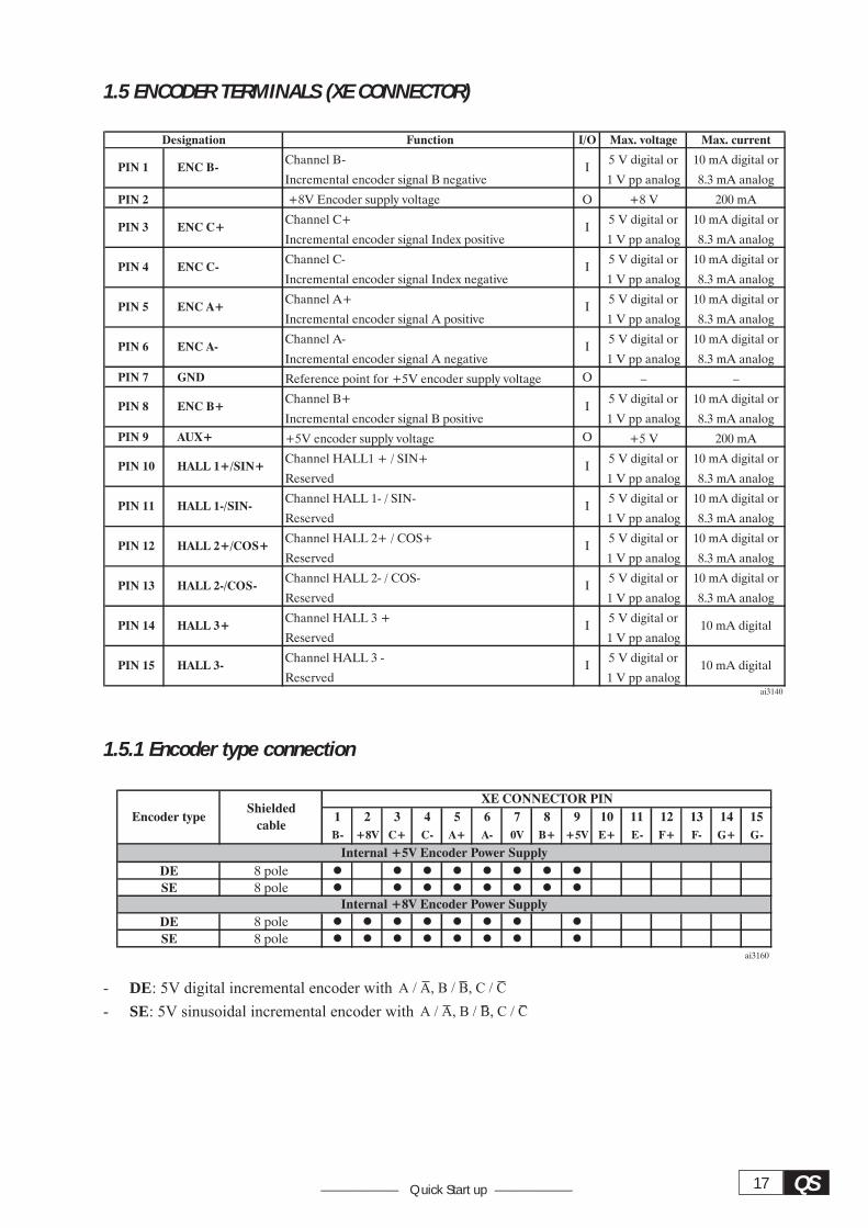
1.5 ENCODER TERMINALS (XE CONNECTOR)
Function I/O Max. voltage Max. current
Channel B- 5 V digital or 10 mA digital or
Incremental encoder signal B negative 1 V pp analog 8.3 mA analog
PIN 2 +8V Encoder supply voltage O +8 V 200 mA
Channel C+ 5 V digital or 10 mA digital or
Incremental encoder signal Index positive 1 V pp analog 8.3 mA analog
Channel C- 5 V digital or 10 mA digital or
Incremental encoder signal Index negative 1 V pp analog 8.3 mA analog
Channel A+ 5 V digital or 10 mA digital or
Incremental encoder signal A positive 1 V pp analog 8.3 mA analog
Channel A- 5 V digital or 10 mA digital or
Incremental encoder signal A negative 1 V pp analog 8.3 mA analog
PIN 7 GND Reference point for +5V encoder supply voltage O – –
Channel B+ 5 V digital or 10 mA digital or
Incremental encoder signal B positive 1 V pp analog 8.3 mA analog
PIN 9 AUX+ +5V encoder supply voltage O +5 V 200 mA
Channel HALL1 + / SIN+ 5 V digital or 10 mA digital or
Reserved 1 V pp analog 8.3 mA analog
Channel HALL 1- / SIN- 5 V digital or 10 mA digital or
Reserved 1 V pp analog 8.3 mA analog
Channel HALL 2+ / COS+ 5 V digital or 10 mA digital or
Reserved 1 V pp analog 8.3 mA analog
Channel HALL 2- / COS- 5 V digital or 10 mA digital or
Reserved 1 V pp analog 8.3 mA analog
Channel HALL 3 + 5 V digital or
Reserved 1 V pp analog
Channel HALL 3 - 5 V digital or
Reserved 1 V pp analogai3140
HALL 2+/COS+
HALL 2-/COS-
HALL 3+
HALL 3-
Designation
ENC B-
ENC C-
ENC A+
ENC C+
PIN 1
PIN 3
PIN 4
PIN 5
10 mA digital
10 mA digitalPIN 14
I
I
I
PIN 15 I
PIN 12
PIN 13
I
I
I
I
PIN 10
PIN 11
I
IHALL 1-/SIN-
HALL 1+/SIN+
I
I
PIN 6
PIN 8
ENC A-
ENC B+
1.5.1 Encoder type connection
1 2 3 4 5 6 7 8 9 10 11 12 13 14 15
B- +8V C+ C- A+ A- 0V B+ +5V E+ E- F+ F- G+ G-
DE 8 pole � � � � � � � �
SE 8 pole � � � � � � � �
DE 8 pole � � � � � � � �
SE 8 pole � � � � � � � �
ai3160
Internal +8V Encoder Power Supply
XE CONNECTOR PIN
Encoder typeShielded
cable
Internal +5V Encoder Power Supply
- DE: 5V digital incremental encoder with A / A, B / B, C / C
- SE: 5V sinusoidal incremental encoder with A / A, B / B, C / C
18QS AVy -HGB
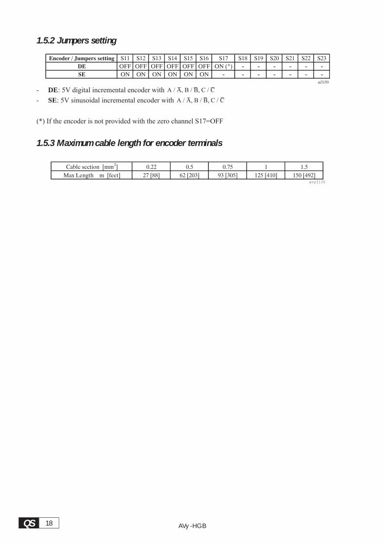
1.5.2 Jumpers setting
Encoder / Jumpers setting S11 S12 S13 S14 S15 S16 S17 S18 S19 S20 S21 S22 S23
DE OFF OFF OFF OFF OFF OFF ON (*) - - - - - -
SE ON ON ON ON ON ON - - - - - - -ai3150
- DE: 5V digital incremental encoder with A / A, B / B, C / C
- SE: 5V sinusoidal incremental encoder with A / A, B / B, C / C
(*) If the encoder is not provided with the zero channel S17=OFF
1.5.3 Maximum cable length for encoder terminals
Cable section [mm2] 0.22 0.5 0.75 1 1.5
Max Length m [feet] 27 [88] 62 [203] 93 [305] 125 [410] 150 [492]avy3130
QS19—————— Quick Start up ——————
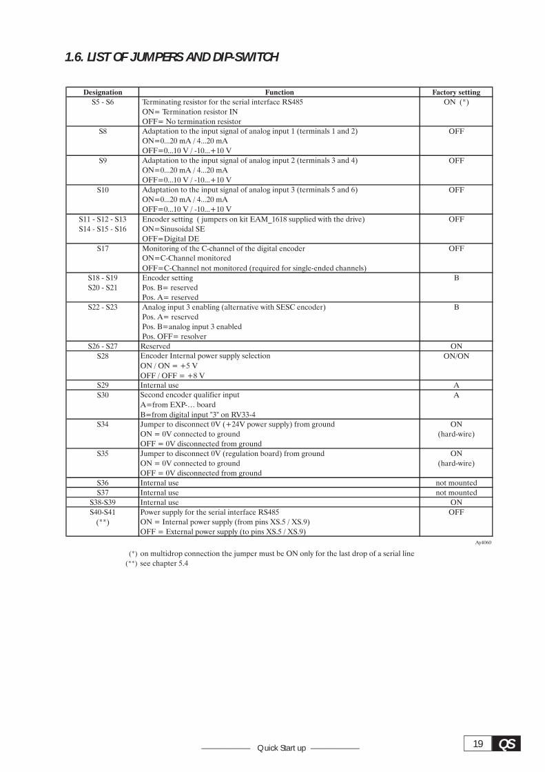
1.6. LIST OF JUMPERS AND DIP-SWITCH
Designation Function Factory setting
S5 - S6 Terminating resistor for the serial interface RS485 ON (*)
ON= Termination resistor IN
OFF= No termination resistor
S8 Adaptation to the input signal of analog input 1 (terminals 1 and 2) OFFON=0...20 mA / 4...20 mA
OFF=0...10 V / -10...+10 V
S9 Adaptation to the input signal of analog input 2 (terminals 3 and 4) OFFON=0...20 mA / 4...20 mA
OFF=0...10 V / -10...+10 V
S10 Adaptation to the input signal of analog input 3 (terminals 5 and 6) OFFON=0...20 mA / 4...20 mA
OFF=0...10 V / -10...+10 V
S11 - S12 - S13 Encoder setting ( jumpers on kit EAM_1618 supplied with the drive) OFF
S14 - S15 - S16 ON=Sinusoidal SE
OFF=Digital DE
S17 Monitoring of the C-channel of the digital encoder OFFON=C-Channel monitored
OFF=C-Channel not monitored (required for single-ended channels)
S18 - S19 Encoder setting B
S20 - S21 Pos. B= reserved
Pos. A= reserved
S22 - S23 Analog input 3 enabling (alternative with SESC encoder) B
Pos. A= reserved
Pos. B=analog input 3 enabled
Pos. OFF= resolver
S26 - S27 Reserved ON
S28 Encoder Internal power supply selection
ON / ON = +5 V
OFF / OFF = +8 V
ON/ON
S29 Internal use A
S30 Second encoder qualifier input
A=from EXP-… board
B=from digital input "3" on RV33-4
A
Jumper to disconnect 0V (+24V power supply) from ground ON
ON = 0V connected to ground (hard-wire)
OFF = 0V disconnected from ground
Jumper to disconnect 0V (regulation board) from ground ON
ON = 0V connected to ground (hard-wire)
OFF = 0V disconnected from ground
S36 Internal use not mounted
S37 Internal use not mounted
S38-S39 Internal use ON
Power supply for the serial interface RS485 OFF
ON = Internal power supply (from pins XS.5 / XS.9)
OFF = External power supply (to pins XS.5 / XS.9)
Ay4060
(*) on multidrop connection the jumper must be ON only for the last drop of a serial line(**) see chapter 5.4
S40-S41
(**)
S34
S35
20QS AVy -HGB
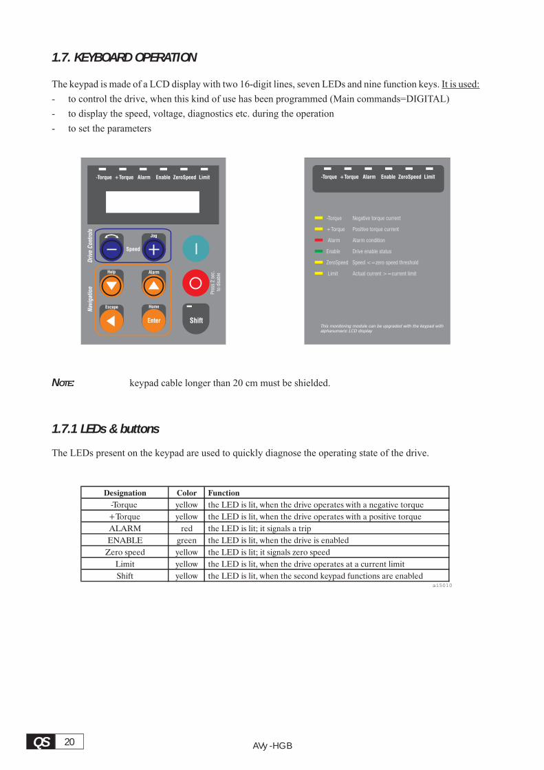
1.7. KEYBOARD OPERATION
The keypad is made of a LCD display with two 16-digit lines, seven LEDs and nine function keys. It is used:
- to control the drive, when this kind of use has been programmed (Main commands=DIGITAL)
- to display the speed, voltage, diagnostics etc. during the operation
- to set the parameters
-Torque +Torque Alarm Enable ZeroSpeed Limit
-Torque Negative torque current
+Torque Positive
Alarm Alarm condition
Enable Drive enable status
ZeroSpeed Speed <=zero speed threshold
Limit Actual current >=current limit
torque current
This monitoring module can be upgraded with the keypad with
alphanumeric LCD display
NOTE: keypad cable longer than 20 cm must be shielded.
1.7.1 LEDs & buttons
The LEDs present on the keypad are used to quickly diagnose the operating state of the drive.
Designation Color Function
-Torque yellow the LED is lit, when the drive operates with a negative torque
+Torque yellow the LED is lit, when the drive operates with a positive torque
ALARM red the LED is lit; it signals a trip
ENABLE green the LED is lit, when the drive is enabled
Zero speed yellow the LED is lit; it signals zero speed
Limit yellow the LED is lit, when the drive operates at a current limit
Shift yellow the LED is lit, when the second keypad functions are enabledai5010
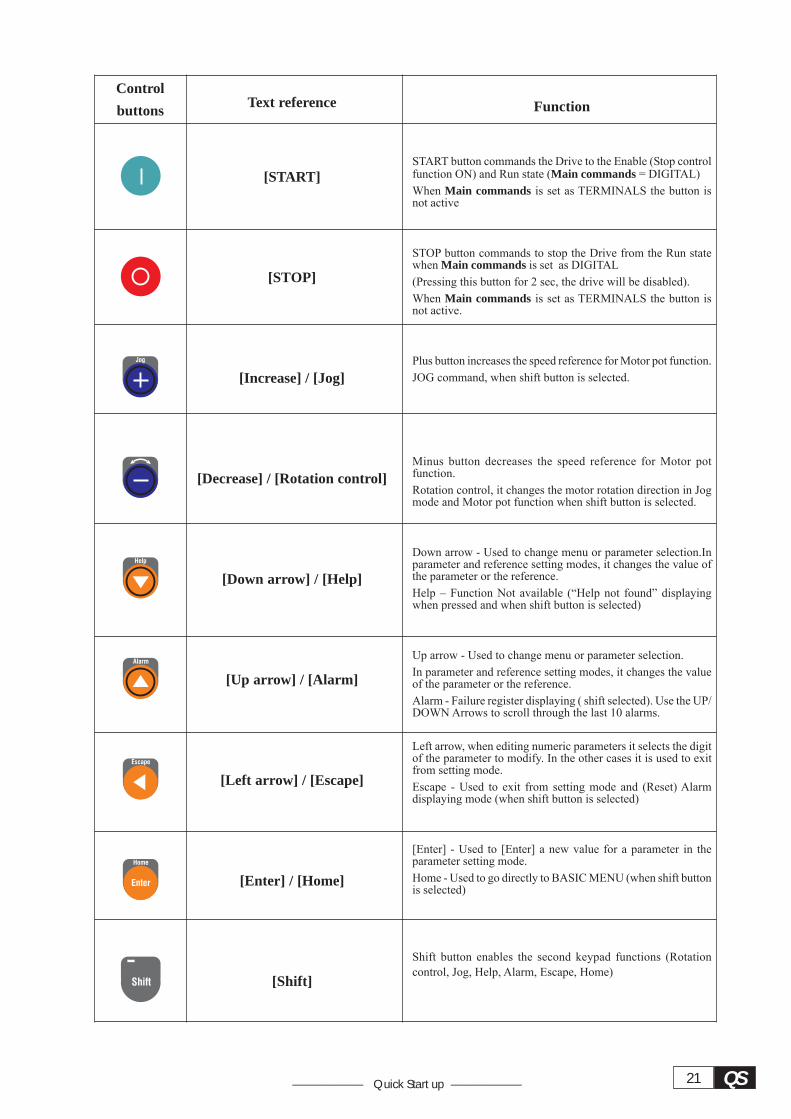
QS21—————— Quick Start up ——————
Control
buttons
Jog
Help
Alarm
Escape
Home
Enter
Shift
Text reference
[START]
[STOP]
[Increase] / [Jog]
[Decrease] / [Rotation control]
[Down arrow] / [Help]
[Up arrow] / [Alarm]
[Left arrow] / [Escape]
[Enter] / [Home]
[Shift]
Function
START button commands the Drive to the Enable (Stop controlfunction ON) and Run state (Main commands = DIGITAL)
When Main commands is set as TERMINALS the button isnot active
STOP button commands to stop the Drive from the Run statewhen Main commands is set as DIGITAL
(Pressing this button for 2 sec, the drive will be disabled).
When Main commands is set as TERMINALS the button isnot active.
Plus button increases the speed reference for Motor pot function.
JOG command, when shift button is selected.
Minus button decreases the speed reference for Motor potfunction.
Rotation control, it changes the motor rotation direction in Jogmode and Motor pot function when shift button is selected.
Down arrow - Used to change menu or parameter selection.Inparameter and reference setting modes, it changes the value ofthe parameter or the reference.
Help – Function Not available (“Help not found” displayingwhen pressed and when shift button is selected)
Up arrow - Used to change menu or parameter selection.
In parameter and reference setting modes, it changes the valueof the parameter or the reference.
Alarm - Failure register displaying ( shift selected). Use the UP/DOWN Arrows to scroll through the last 10 alarms.
Left arrow, when editing numeric parameters it selects the digitof the parameter to modify. In the other cases it is used to exitfrom setting mode.
Escape - Used to exit from setting mode and (Reset) Alarmdisplaying mode (when shift button is selected)
[Enter] - Used to [Enter] a new value for a parameter in theparameter setting mode.
Home - Used to go directly to BASIC MENU (when shift buttonis selected)
Shift button enables the second keypad functions (Rotationcontrol, Jog, Help, Alarm, Escape, Home)
22QS AVy -HGB
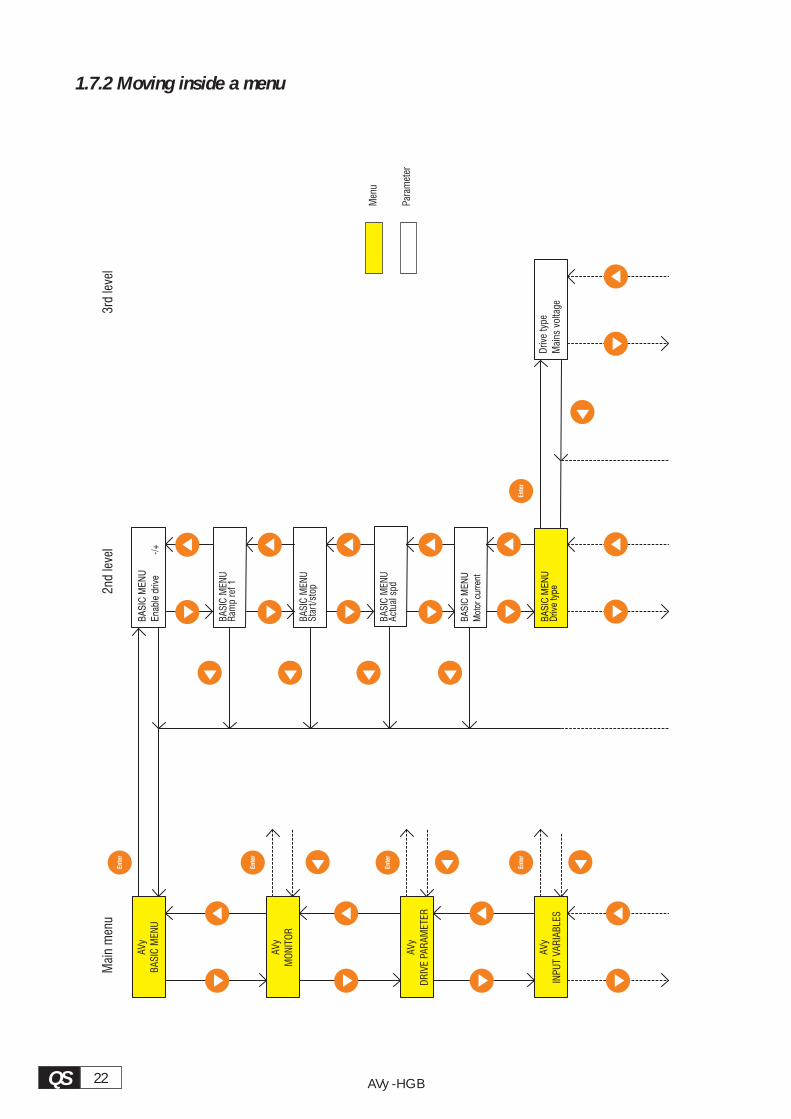
1.7.2 Moving inside a menu
Ent
er
AV
y
BA
SIC
MEN
U
AV
y
MO
NIT
OR
AV
y
DR
IVE
PAR
AM
ETER
AV
y
INP
UT
VA
RIA
BLE
S
Mai
nm
enu
BA
SIC
ME
NU
Ena
ble
driv
e-/
+
Men
u
Para
met
er
BA
SIC
ME
NU
Mot
orcu
rren
t
BA
SIC
ME
NU
Driv
ety
peD
rive
type
Mai
nsvo
ltage3rd
leve
l2n
dle
vel
BA
SIC
MEN
UR
amp
ref
1
BA
SIC
MEN
US
tart
/sto
p
Ent
er
Ent
er
Ent
er
BA
SIC
MEN
UA
ctua
l spd
Ent
er
QS23—————— Quick Start up ——————
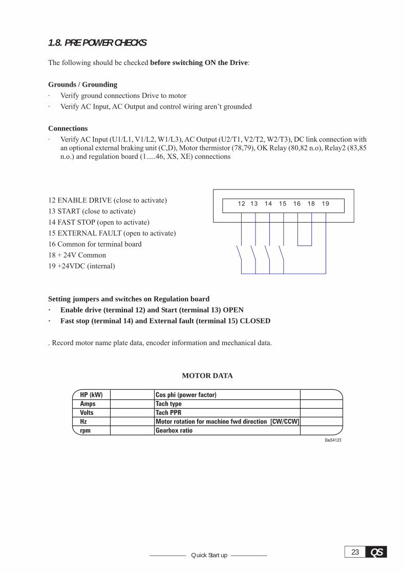
1.8. PRE POWER CHECKS
The following should be checked before switching ON the Drive:
Grounds / Grounding
· Verify ground connections Drive to motor
· Verify AC Input, AC Output and control wiring aren’t grounded
Connections
· Verify AC Input (U1/L1, V1/L2, W1/L3), AC Output (U2/T1, V2/T2, W2/T3), DC link connection withan optional external braking unit (C,D), Motor thermistor (78,79), OK Relay (80,82 n.o), Relay2 (83,85n.o.) and regulation board (1.....46, XS, XE) connections
12 ENABLE DRIVE (close to activate)
13 START (close to activate)
14 FAST STOP (open to activate)
15 EXTERNAL FAULT (open to activate)
16 Common for terminal board
18 + 24V Common
19 +24VDC (internal)
Setting jumpers and switches on Regulation board
· Enable drive (terminal 12) and Start (terminal 13) OPEN
· Fast stop (terminal 14) and External fault (terminal 15) CLOSED
. Record motor name plate data, encoder information and mechanical data.
MOTOR DATA
HP (kW)
Amps
Volts
Hz
rpm
Cos phi (power factor)
Tach type
Tach PPR
Motor rotation for machine fwd direction [CW/CCW]
Gearbox ratio
Dai54123
24QS AVy -HGB
1.9. QUICK TUNING
1. After a complete check of wiring and inputvoltage levels and then turn the power on:
·Verify the following voltages must be present:
Terminal 7, +10V to terminal 9 (on regulationboard)
Terminal 8, -10V to terminal 9 (on regulationboard)
Terminal 19, +24…30V to terminal 18 (onregulation board)
·Check DC link voltage by pressing [Downarrow] to get “MONITOR”, then [Enter], then[Down arrow] to“measurements”, then [Enter],then [Down arrow] to “DC link voltage”, then[Enter].
The value should be:
480-650 vdc for 400 vac input
550-715 vdc for 460 vac input
If it is not within these values, check your linevoltage, as it is unlikely the drive will workproperly.
2. Default to Factory Values: If you are not alreadycertain of the drive configuration, it is necessary todefault to factory values or copy in a file from a PCto be certain you are starting from a knownconfiguration. To default to factory values:
· Default to working memory: Push [Leftarrow] to get back to “MONITOR”, then [Downarrow] to “SPEC FUNCTIONS” and then [Enter].Push [Down arrow] to “Load Default” and[Enter]. The factory values will now be loadedinto working memory for all parameters but theprevious values are still in permanent memory.
3. Set Line Voltage:
· Press [Left arrow] to “SPEC FUNCTIONS”then [Up arrow] to “BASIC MENU”, then[Enter], then [Down arrow] to “Drive type”,then [Enter] to “Mains voltage” and [Enter].Now using the [Up arrow] / [Down arrow] keys,change the voltage value closest to your nominalAC input rating. Then [Enter] to set the value.
4. Adaption to maximum ambient temperature:
· Press [Down arrow] to “Ambient temp” then[Enter]. Now using the [Up arrow] / [Downarrow] keys, set the maximum ambienttemperature value: 40°C or 50°C, then [Enter].
5. Load Default Motor Values:
· Press [Left arrow] until back to “BASICMENU” and then [Down arrow] to “DRIVEPARAMETER”, then [Enter], then [Downarrow] to “Motor Parameter”, [Enter], then[Down arrow] to “Load Motor Par” and [Enter].Use the [Up arrow]/[Down arrow] keys until thedisplay is the correct motor voltage, then [Enter].For 460 VAC motors, select 460, and for 380/400VAC motors select 400.
6. Set Actual Motor Data:
· Press [Left arrow] until back to “DRIVEPARAMETER”, then [Enter] to get “Mot platedata” and [Enter] to “Nominal Voltage” then[Enter] again to see the value. Using the [Uparrow]/[Down arrow] keys to change the valueand the [Left arrow] to move the characterposition. When correct press [Enter].
· Press [Down arrow] to “Nominal speed”,[Enter], then use the [Up arrow] / [Downarrow] keys to get the nominal speed on themotor nameplate. Press [Enter] to set data. Note,some manufacturers of vector motors put thesynchronous speed (exactly 600, 900, 1500,1800, 3600) for the nominal speed, rather thanthe slip speed it would run if run on 50 Hz power.If this is done, you MUST put a slip speed in thisdata. Figure 20 rpm less than the synchronousspeed for these cases.
· Press [Down arrow] to “Nom frequency” and[Enter] and set to the nominal frequency on thenameplate (50 or 60 Hz usually) by using the[Up arrow] / [Down arrow] keys. Press [Enter]to set data.
· Press [Down arrow] to “Nominal current” and[Enter] and set to the nominal current on the motornameplate (rated current) by using the [Up arrow]/ [Down arrow] keys. Press [Enter] to set data.
· Press [Down arrow] to “Cos phi” and [Enter]and set to the nominal power factor on thenameplate by using the [Up arrow] / [Downarrow] keys (accept the default if you don’tknow). Press [Enter] to set data.
· Press [Down arrow] to “Base Voltage” and[Enter] and set to the base voltage by using the[Up arrow] / [Down arrow] keys (usually ratedvoltage). Press [Enter] to set data. Look in themanual for both Base Voltage and BaseFrequency when operating the motor abovenormal synchronous speed.
· Press [Down arrow] to “Base Frequency” and[Enter], set to the base frequency by using the[Up arrow] / [Down arrow] keys (usually ratedfrequency). Press [Enter] to set data.
QS25—————— Quick Start up ——————
· Press [Down arrow] to “Take motor par” and[Enter] and set all the motor parameters. If, whenyou do this, a message saying “Over-rangeerror XXX” appears, there is something wrongwith the data you have entered. The drive hasNOT ACCEPTED the values you have entered.The most common cause of this is trying to[Enter] a value for “Nominal Current that is lessthan 30% of the drive rating. This is not alloweddue to problems in control of a large drive on avery small motor. Try to go back to the beginningof step 6 and repeat the entries. If this doesn’twork, see Overflow list in chapter 1.12,“Troubleshooting” or contact your service office.
7. Set Drive Base Values:
· Press [Left arrow] until back to “driveparameter” then [Down arrow] to“configuration”, then [Enter].
· Press [Down arrow] to “Speed Base Value”then [Enter] and set the nameplate rated full loadspeed on the motor nameplate, press [Enter].
· Press [Down arrow] to “full load current” then[Enter] and set the DRIVE (not motor) rated fullload current on the drive nameplate by using the[Up arrow] / [Down arrow] keys, then press[Enter] to set.
8. Set Regulation Mode: (V7f, Sensorless vect orField oriented mode )
· Press [Up arrow] to “Regulation mode”, then[Enter] and use [Up arrow] / [Down arrow]keys to select “sensorless vect” or “Fieldoriented” then [Enter].
· If “Field oriented” mode is select:
· Press [Down arrow] until to “Motor spd fbk”,then press [Enter], [Down arrow] to “Encoder1 type”, then [Enter]. Use the [Up arrow]/[Down arrow] keys to select sinusoidal encoderor digital encoder, then [Enter].
· Press [Down arrow] to “Encoder 1 pulses”, then[Enter] and set the value using the [Up arrow]/[Down arrow] keys to the ppr (pulses perrevolution) of your encoder (usually 1024), [Enter].
9. Speed Limit:
· Press [Left arrow] until “Basic Menu”, then[Down arrow] to “Limits”, then [Enter] for“Speed Limits”, then [Enter] for “SpeedAmount”, then [Enter] to “Speed Min Amount”.Press [Down arrow] to “Speed Max Amount”,and [Enter]. Change the value from 5000 rpmto the maximum speed of the motor using the[Up arrow]/[Down arrow] keys as before (fornow set it to 105% of the rated motor speed).Press [Enter].
10. Prepare for Self Tune:
The keypad will be used for this purpose but theI/O needs to be connected properly so thehardware enable/disable functions.
11. Save Parameters:
· Press [Left arrow] until to “limits”, then [Uparrow] until “Basic Menu” then [Enter], then[Down arrow] to “save parameters”, then[Enter].
The display will read “wait” until the values arepermanently stored.
12. Self Tune:
Make sure power is on and drive not enabled.
Close the switch on terminal 12 (hardware enablehas 24 Vdc on it).
· When the enable switch is made, Press [Leftarrow] until “Basic Menu” then [Down arrow]to “Drive Parameter”, then [Enter], then [Downarrow] to “motor parameters” and [Enter].Press “[Down arrow] to “Self Tuning” and[Enter] to see “self tune 1”. Press [Enter] to see“start part 1” and [Enter], “start part 1 ?” and[Enter] again. The keypad should show the“enable” led illuminated, if not, make sure thatyou have the jumpers (or external switches) setso that 24 Vdc exists on 12, 13, 14, 15, withrespect to 16 or 18.
· You should now see “measuring Rs” (statorresistance). Wait until the display says “end”,then disable the drive (open the switch to 12)and push [Left arrow] twice to see “self tune1”, press [Enter], then [Down arrow] all theway to “take val part 1” and [Enter]. The displaywill read “wait” until the values are stored.
NOTE: “xxx range error” or “timeout” messagesmay also occur in some extreme parameterranges. Repeat execution in this case. Iferror messages are persistent seetroubleshooting section.
13. Self Tune part 2:
The initial part of self tuning that can be donewithout the motor rotating has beenaccomplished, now in order to get the bestpossible tuning, the motor needs to be free toturn with no load attached to the shaft. For thiswe use Self tune mode 2a. If, for any reason, themotor cannot be made free to rotate with no load,then a “close” level of tuning can still beaccomplished by selecting Self tune mode 2b.
· Now press [Left arrow] to see “self tune 1”then [Down arrow] to “self tune 2a or 2b andpress [Enter]. Enable the drive using the switch
26QS AVy -HGB
to terminal 12. Press [Enter], “start part 2a ?”or “start part 2b ?” then [Enter] and see “measuresat 2a (or b)” will appear and the motor shaftwill turn (if “self tune 2a” is select). Wait untilthe display says “end”, press [Left arrow] tosee “self tune 2a (or b)” then [Enter] and press[Down arrow] to see “take val part 2a (or b)”.Disable the drive (switch off terminal 12), then[Enter].
NOTE: “xxx range error” or “timeout” messagesmay also occur in some extreme parameterranges. Repeat execution in this case. Iferror messages are persistent seetroubleshooting section.
If there was some reason you did not wantto keep these values permanently, but onlywanted to try to run the drive with them,there is no need to save to permanentmemory. If power is cycled however, thesevalues just obtained will be lost unless thenext step is taken.
14. Self tune part 3:
The third part of self tuning (Speed regulatortuning) identifies the total inertia value at the motorshaft, the friction value and computes theproportional and integral gains of the speedregulator. The motor needs to be free to turn withload attached to the shaft.
WARNING !This procedure requires free rotation of themotor shaft coupled to the load. Start/Stopcommand is disregarded, therefore it can notbe used on drives with limited travel.
CAUTION !The test is performed using the torque limitvalue set in Test T curr lim parameter. Thetorque is applied stepwise, with no ramp(profile), therefore the mechanical transmis-sion must not have significant backlash, andit must be compatible with operation at thetorque limit set in Test T curr lim parameter.The user can reduce the torque limit to asuitable value via the Test T curr limparameter.
NOTE ! - Application where the system inertia cou-pled to the motor shaft is much higher thanthe motor inertia value , increase the Test Tcurr lim parameter to avoid “Time out” error.
- This procedure is not suitable for usewith “hoist” or “elevator” drives.
- Encoder feedback is required when Fieldoriented mode is selected.
- Set the current limit (BASIC MENU\ TCurrent lim +/-) to a value compatible withthe motor size and load. (Example whenmotor is 1/3 of the Drive power, the limitshould be reduced compared to the defaultvalue).
- Select the torque current value to be usedduring the test via the Test T curr limparameter
· Now press [Left arrow] to see “self tune 2aor 2b” then [Down arrow] to “self tune 3” andpress [Enter] to Fwd-Rev spd tune, then [Enter],set the motor shaft direction for this test: Forwardor Reverse by using [Up arrow] / [Down arrow]keys. Press [Enter] to set the selection.
· Enable the drive using the switch to terminal12 [and close terminal 13 to terminal 19 if Speedcontrol function is enabled (default)]. Press[Down arrow] to “Start part 3” then press[Enter], “start part 3 ?” then [Enter] and see“measure speed” will appear and the motor willturn. Wait until the display says “end”, press [Leftarrow] to see “self tune 3” then [Enter] and press[Down arrow] to see “take val part 3”. Disablethe drive, then [Enter]. You are now finished withthe initial set up and tuning with values stored inonly in the “working memory”.
NOTE: “xxx range error” or “timeout” messagesmay also occur in some extreme parameterranges. Repeat execution in this case. Iferror messages are persistent see chapter1.12, “Troubleshooting”
NOTE: If there was some reason you did not wantto keep these values permanently, but onlywanted to try to run the drive with them,there is no need to save to permanentmemory. If power is cycled however, thesevalues just obtained will be lost. To saveall values to permanent memory, selectSave parameters and press [Enter] .
15. Set up for Running:
First, before saving, let’s put the drive into theconfiguration you want to run it in.
The drive is factory setting to run through anexternal +/- 10V reference using a potentiometerconnected to terminals 1, 2 (see table 5.3.2.1). Ifyou would like to run the motor using the keypadthrough the Increase [+] and Decrease [-] keys(Enable motor pot parameter = Enabled), seethe following instruction to run.
If a change of the default acceleration / decel-eration ramp time value is needed, using the Accdelta time / Acc delta speed and Dec delta time/ Dec delta speed is possible to set the desideredvalue.

QS27—————— Quick Start up ——————
1.9.1 Motor Potentiometer
NOTE! (Main commands = DIGITAL)
Enable drive, terminal 12 to24Vdc
Start, terminal 13 to 24Vdc
Resetting the speed reference value using Mot potfunction
· Press [STOP] button to stop the motor
· Press [Left arrow] until to “Basic menu”, then[Down arrow] to “Functions”. [Enter] to motorpot, then [Enter] to “enab motor pot”, press[Down arrow] to motor pot reset, then [Enter].
The diplay will read “ready” until the referencevalue is set to zero.
Set motor pot disable (Enable motor pot parameter= Disable) if you will want to use an analog voltage(pot or otherwise) into terminal 1 for speed reference(already factory set).
Jog function
NOTE! This function is already standardsetting enabled. (Enable jog pa-rameter = Enabled) with a speedreference value = 100 rpm.
(Main commands = DIGITAL)
Enable drive, terminal 12 to 24Vdc
Start, terminal 13 to 24Vdc
Press [SHIFT and [+] to run, the speed will bedisplayed
Press [-] to select the motor shaft rotation
Press [jog] to run the other direction
Press [Left arrow] to exit from jog operation
Changing jog reference
Press [Down arrow] until “Functions”, [Enter], then[Down arrow] until “Jog reference”, [Enter], usingthe [Up arrow]/[Down arrow] keys to change thevalue and the [Left arrow] to move the characterposition, set the reference value, then [Enter].
If there are other changes you might want to maketo set up (see Optional Things), do them now,and complete the following step to put everythinginto permanent memory.
Saving all values to Permanent Memory:
. Press [Left arrow] back to “Configuration”then [Up arrow] to “basic menu” and [Enter].Press [Down arrow] to “save parameters” and[Enter]. Parameters are now stored permanently.
Control buttons
Jog
Shift
Sequencing
Press START button to command the Drive to the Enableand Run state
Press STOP button commands to stop the Drive from theRun state
Press to display the current reference value and to increasethe reference value and accelerate the drive.
Press to decrease the reference value and decelerate thedrive.
Press SHIFT and [-] to change the motor shaft rotation
Display
Motor pot oper
+0 [rpm] POS
Motor pot oper
-0 [rpm] NEG

28QS AVy -HGB
1.10 OPTIONAL THINGS
Encoder verification: Set the Drive in V/f mode andrun the motor, enable and start the drive and set ananalog reference. If the reference is positive onterminal 1 with respect to 2 (common) the motorshould be turning clockwise. With the motor turningclockwise (looking at the driving shaft pointing atyou.) (you can even do this by hand while notenabled), monitor the encoder measurement byclicking “Monitor/measurements/speed/speed in rpm/Enc 1 speed”. The speed should be positive, notnegative. If it is negative, then A and A- or B and B-should be interchanged on the encoder. Now returnto the “Set Up for Running” section.
Current Limit: The current limit will have been setto approximately 136% by default in the previous setup(exact number is a function of the power factor but thedifference is very small). The value actually set canbe verified by (from “Basic Menu”) pressing down/right arrow to “Limits”, then [Enter], then down/rightarrow to “current limits”, then [Enter], then down rightarrow to “T current lim” and [Enter]. The value of Tcurrent limit can be changed if you like to a higher (orlower) number. Bear in mind that the ultimate limitsare based on the capacity of the drive, not the motor.T current is the torque producing component of totalcurrent. Settings in excess of 200% are possible,although the motor may not be able to handle thiscurrent. Most motors are rated only for 150% for 1minute. The drive will protect itself though anintelligent temperature, voltage, I2T algorithmregardless of how you set this number. The drive willprovide 150% of the value in “Configuration/Full LoadCurrent” for 1 minute (200 % for a short time).
I/O Configuration: This drive can be configured invirtually any imaginable way.
The standard drive has three standard analog inputsand gives you two analog outputs as well as six digitalinputs and two digital outputs which are assignableand configurable. The drive is defaulted alreadyto provide the analog outputs as Actual speed andload (Torque current), but may require some scaling.To set up the drive for two analog outputs (one forspeed and one for load) for metering or otherpurposes, do the following:
Refer to the “Control terminals” section of thisguide showing a description of the connection ofthe regulation section and how to make them. Amore detailed description and discussion of the I/O are showed in the manual. The analog outputsare defaulted to a scale of 1, which means 10 voltsout at max parameter value. In other words, if
analog output 1 is set to maximum speed then maxspeed will be scaled 10 Vdc (maximum outputvoltage available) at “Speed Base Value” (foundunder Configuration). If you wanted 5 volts out atmax speed then set the scale to 0.5. If the outputwas set to Torque current (the torque producingcurrent, which is the part of the total motor currentthat actually produces torque), then 10 Vdc wouldbe rated current. If you wanted the output to be10 Vdc at 150% of “Full Load Current” (foundunder Configuration) then the scale would be 0.66.The standard factory default is already set up toput out speed (with scale factor of 1) on analogoutput 1 (terminals 21 and 22) and load (Torquecurrent, with scale factor of 1) on analog output 2(terminals 23 and 22). Note that terminal 22 is acommon for both the outputs. This common canbe grounded, and should be grounded somewhere,preferably at the load device (meter).
How to disable analog input 1 as ramp reference:(Analog inputs 2 and 3 are already off from default,#1 is defaulted to Ramp ref 1). This is being donenow to allow us to use the keypad to set speed indigital way.
· Press [Up arrow]/[Down arrow] to “I/OConfig”, then [Enter].
· Press [Down arrow] to “Analog inputs”, then[Enter] for Analog input 1, then [Enter] to Selectinput 1, then [Enter] to display the setting, whichwill be “Ramp ref 1”.
· Press [Up arrow] / [Down arrow] keys until“OFF” is displayed, then [Enter].
How to enable analog input 2 as ramp reference
· Press [Up arrow]/[Down arrow] to “I/OConfig” and press [Enter], then down right arrowto “Analog inputs” then [Enter] for “Analoginput 1” then [Down arrow] to ”analog input 2then [Enter] to “select input 2”, then [Enter]again to see the set up. It says “OFF”. Use the[Up arrow] / [Down arrow] keys to display“Ramp ref 1” (if this setting is not already used,or “Ramp ref 2”) and [Enter]. This means theAnalog input 2 (terminals 3 and 4) will be theramped (accel/decel) speed reference for thedrive.
The AVy manual on CD-ROM shows the entire con-figuration of the I/O and other set up for the drive. Itthis does not help, call the customer service and wecan help you with your specific configuration.
QS29—————— Quick Start up ——————
1.11 QUICK TUNING GUIDE FORFACTORY CONFIGURED (OR PRE-CONFIGURED) DRIVES
When the drive configuration has already been setand you are simply tuning a motor which has notbeen tuned, you can ignore most of the precedingprocedure, since it has already been done, but unlessyou are certain, it is recommended that you gothrough the steps anyway, just to verify that the datashown in the various locations indicated is OK. Youcan just use the [Left arrow] key rather than the[Enter] key in all the steps in which the entry is foundto be correct. Start with step 4 of the full procedureand do not default the parameters to factoryparameters. If there is any question about whetherthe existing setup should be saved or not, then usethe configuration tool software that came with thedrive and save the file to a PC first so it can be usedlater. Normally, drives configured at the factory willhave the setup file already saved to your configura-tion tool diskette.
30QS AVy -HGB
1.12 TROUBLESHOOTING
Overflow list
CODE CAUSES
10 ; 54 The ratio between the Encoder 1 pulses[416] and the number of motor poles pair must behigher than 128
3 ; 4 The Stator resistance [436] value is too high. The motor is not compatible with the drivesize used.
5 ; 8 ; 9 ; 15 The Leakage inductance [437] value is too high. The motor is not compatible with thedrive size used.
16 ; 24 The Rotor resistance [166] value is too high. The motor is not compatible with the drivesize used.
17 The Nominal voltage [161] and Nom frequency [163] values produce motor nominal flux(out of range) that is too high.
- Verify these values: the Nominal voltage value is too high and/or the Nom Frequencyvalue is too small.
18 The Base voltage [167] and Base frequency [168] values produce motor nominal flux (out ofrange) that is too high.
- Verify these values: the Base voltage value is too high and/or the Base frequency valueis too small
23 The ratio between nominal flux (Nominal voltage, Nom frequency) and working flux (Basevoltage , base frequency) is too high.
- Verify the above parameters value.
The Magnetizing current [165] value is too high.
- Verify that this value is lower than Full load curr.
27 The Base voltage value is too high. The maximum value is 500V.
28 The Base frequency value is too high. This value must be lower than 500Hz
59 The Magnetizing working curr [726] is too high.
- Verify that the nominal flux value (Nominal voltage and Nom frequency) is lower thanthe working flux value (Base voltage and Base frequency). Check the parameters value.
The Magnetizing current value is too high.
- Verify that this value is lower than Full load curr.
64 The Motor cont curr [656] value, of the motor thermal protection function (menu Ovldmot contr), produces continuative current that is too low in comparison to the used invertersize. This error can also be due to a too low setting of the Nominal current [164] parameter(0.3 x I
2N).
66 The Nominal speed [162] value is wrong.
The set value produces too small (or too high) slip value.

QS31—————— Quick Start up ——————
LIST OF SELF TUNE ERROR MESSAGES
- Generic messages
Description Note
“Drive disabled”: Provide enable input by setting terminal 12 high.
“Not ready”: “Take values part 1” or “Take values part 2a” or “Take values part 2b”or “Takevalues part 3” can not be executed because the measurement has not been completedcorrectly. Repeat self tune procedure.
“Time out”: Measurement has not been completed in the proper time.
“Start part…?”: Press [ENTER] to confirm start of measurement.
“Tuning aborted”: Measurement aborted by user ([SHIFT] / [Escape] buttons has been pressed).
“Set Main cmd=Dig”: Go to CONFIGURATION menu and set Main commands = digital.
“Set Ctrl=Local”: Go to CONFIGURATION menu and set Control mode = Local.
“Reg mode NOK”: Self tune part 3 can only be executed Regulation mode = Field oriented orRegulation mode = Sensorless vect. Go to BASIC MENU and set Regulationmode properly.
“Inertia range”: Self-tuning part 3 procedure has found an inertia motor value too low, for thisreason it cannot calculate the speed regulator gains. Try to repeat self tune procedureto overcome possible accidental measure error.
If this error persist (inertia is really lower than the measurable minimum value),avoid to give “Take val part 3”command. The speed regulator will be also stablewith the factory gains value. It is possible to optimize the feedback speed by usingthe regulator manual tuning .
- Measurement error messages
These messages may occour when extreme parameter values have to be identified. It can be useful to retrythe self tune command when any of the following messages occours. If messages persist, alternative manualtuning procedures should be adopted.
Description Note
“No break point” Self tune part1 failed. Check integrity of connections between inverter and motorprior to attempt repeating part 1.
“Over speed” Self tune part3 detected a a much higher speed than expected. Possible causes are:load causing a speed drift or bad tuning of inner loops when using Sensorless vectormode. Try repeating Self tune 1 or the corresponding manual tune operations.
“Drive stalled”: Increase value of parameter Test T curr lim and repeat Self tune 3
“Load applied”: Nominal zero load torque at standstill was detected. Self tune 3 is impossible forthis type of load.
“T curr too high”: Reduce value of parameter Test T curr lim for Self tune 3
“Friction null”: Value of friction is zero or lower than the accuracy limit of the control system.
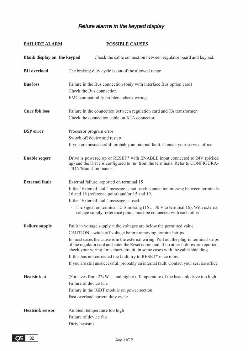
32QS AVy -HGB
Failure alarms in the keypad display
FAILURE ALARM POSSIBLE CAUSES
Blank display on the keypad Check the cable connection between regulator board and keypad.
BU overload The braking duty cycle is out of the allowed range
Bus loss Failure in the Bus connection (only with interface Bus option card)
Check the Bus connection
EMC compatibility problem, check wiring.
Curr fbk loss Failure in the connection between regulation card and TA transformer.
Check the connection cable on XTA connector.
DSP error Processor program error
Switch off device and restart
If you are unsuccessful: probably an internal fault. Contact your service office.
Enable seqerr Drive is powered up or RESET* with ENABLE input connected to 24V (pickedup) and the Drive is configured to run from the terminals. Refer to CONFIGURA-TION/Main Commands.
External fault External failure, reported on terminal 15
If the "External fault" message is not used: connection missing between terminals16 and 18 (reference point) and/or 15 and 19.
If the "External fault" message is used:
- The signal on terminal 15 is missing (15 ... 30 V to terminal 16). With externalvoltage supply: reference points must be connected with each other!
Failure supply Fault in voltage supply = the voltages are below the permitted value
CAUTION: switch off voltage before removing terminal strips.
In most cases the cause is in the external wiring. Pull out the plug-in terminal stripsof the regulator card and enter the Reset command. If no other failures are reported,check your wiring for a short-circuit, in some cases with the cable shielding.
If this has not corrected the fault, try to RESET* once more.
If you are still unsuccessful: probably an internal fault. Contact your service office.
Heatsink ot (For sizes from 22kW ... and higher). Temperature of the heatsink drive too high.
Failure of device fan.
Failure in the IGBT module on power section.
Fast overload current duty cycle.
Heatsink sensor Ambient temperature too high
Failure of device fan
Dirty heatsink

QS33—————— Quick Start up ——————
Intake air ot (For sizes from 22kW ... and higher). Temperature of the cooling air too high.
Failure of device fan(s).
Cooling opening obstructed.
Interrupt error An unused interrupt has occurred
Switch off device and restart
If you are unsuccessful: probably an internal fault. Contact your service office.
Module overtemp (For sizes from 0.75 to 15 kW). Temperature of the IGBT module too high.
Failure of device fan.
Failure in the IGBT module on power section.
Fast overload current duty cycle.
Output stages Internal Overcurrent failure of IGBT power section
Switch off device and restart
If you are unsuccessful, contact your service office.
Overcurrent Overcurrent in the motor circuit
Short-circuit or ground fault at the output of the drive
Current regulator optimized incorrectly
Message appears when switching on the device: drive is engaging a motor that isrunning. Auto capture function must be activated.
Switch off device and restart
If you are unsuccessful, contact your service office.
Overvoltage Overvoltage in intermediate circuit due to energy feedback from motor
Lengthen deceleration ramp. If not possible:
Use a BU... braking unit to reduce the feed
Overtemp Motor Overtemperature of the motor (indicated via thermistor on terminals 78/79)
Cable between thermistor connection on motor and terminals 78 and 79 interrupted.
Overheating of motor:
- Load cycle too extreme
- Ambient temperature at site of motor too high
- Motor has an external fan: fan failed
- Motor does not have an external fan: too large a load at low speeds. The coolingeffect of the fan on the motor shaft is too low for this load cycle. Change cycleor fit external fan.
Regulation ot Temperature of the Regulation card of the Drive too High.
Ambient temperature too high.
Speed fbk loss Speed feedback loss
Encoder not connected, or incorrectly connected or not supplied:
Select the Enc 1 speed parameter in the MONITOR\ Measurement \ Speed \ Speedin rpm menu.
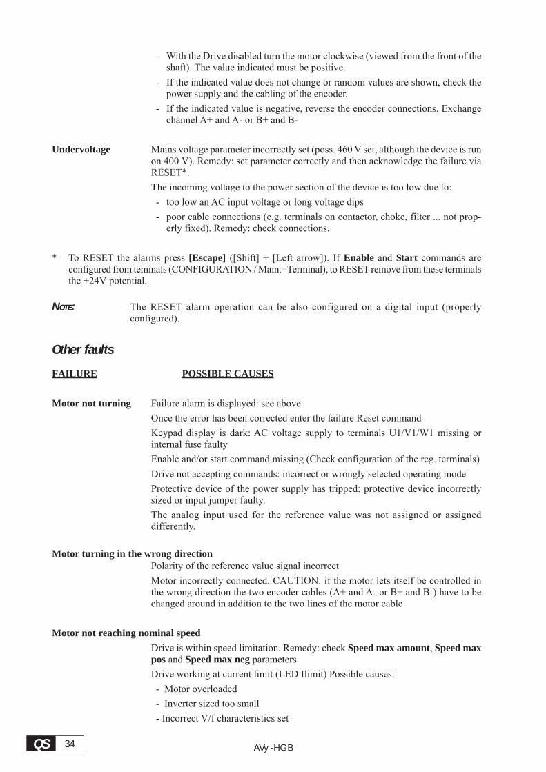
34QS AVy -HGB
- With the Drive disabled turn the motor clockwise (viewed from the front of theshaft). The value indicated must be positive.
- If the indicated value does not change or random values are shown, check thepower supply and the cabling of the encoder.
- If the indicated value is negative, reverse the encoder connections. Exchangechannel A+ and A- or B+ and B-
Undervoltage Mains voltage parameter incorrectly set (poss. 460 V set, although the device is runon 400 V). Remedy: set parameter correctly and then acknowledge the failure viaRESET*.
The incoming voltage to the power section of the device is too low due to:
- too low an AC input voltage or long voltage dips
- poor cable connections (e.g. terminals on contactor, choke, filter ... not prop-erly fixed). Remedy: check connections.
* To RESET the alarms press [Escape] ([Shift] + [Left arrow]). If Enable and Start commands areconfigured from teminals (CONFIGURATION / Main.=Terminal), to RESET remove from these terminalsthe +24V potential.
NOTE: The RESET alarm operation can be also configured on a digital input (properlyconfigured).
Other faults
FAILURE POSSIBLE CAUSES
Motor not turning Failure alarm is displayed: see above
Once the error has been corrected enter the failure Reset command
Keypad display is dark: AC voltage supply to terminals U1/V1/W1 missing orinternal fuse faulty
Enable and/or start command missing (Check configuration of the reg. terminals)
Drive not accepting commands: incorrect or wrongly selected operating mode
Protective device of the power supply has tripped: protective device incorrectlysized or input jumper faulty.
The analog input used for the reference value was not assigned or assigneddifferently.
Motor turning in the wrong directionPolarity of the reference value signal incorrect
Motor incorrectly connected. CAUTION: if the motor lets itself be controlled inthe wrong direction the two encoder cables (A+ and A- or B+ and B-) have to bechanged around in addition to the two lines of the motor cable
Motor not reaching nominal speed
Drive is within speed limitation. Remedy: check Speed max amount, Speed maxpos and Speed max neg parameters
Drive working at current limit (LED Ilimit) Possible causes:
- Motor overloaded
- Inverter sized too small
- Incorrect V/f characteristics set
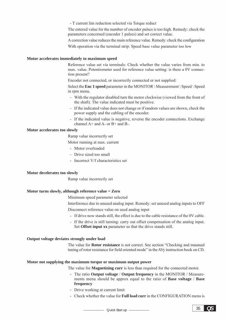
QS35—————— Quick Start up ——————
- T current lim reduction selected via Torque reduct
The entered value for the number of encoder pulses is too high. Remedy: check theparameters concerned (encoder 1 pulses) and set correct value.
A correction value reduces the main reference value. Remedy: check the configuration
With operation via the terminal strip: Speed base value parameter too low
Motor accelerates immediately to maximum speed
Reference value set via terminals: Check whether the value varies from min. tomax. value. Potentiometer used for reference value setting: is there a 0V connec-tion present?
Encoder not connected, or incorrectly connected or not supplied:
Select the Enc 1 speed parameter in the MONITOR \ Measurement \ Speed \ Speedin rpm menu.
- With the regulator disabled turn the motor clockwise (viewed from the front ofthe shaft). The value indicated must be positive.
- If the indicated value does not change or if random values are shown, check thepower supply and the cabling of the encoder.
- If the indicated value is negative, reverse the encoder connections. Exchangechannel A+ and A- or B+ and B-.
Motor accelerates too slowly
Ramp value incorrectly set
Motor running at max. current
- Motor overloaded
- Drive sized too small
- Incorrect V/f characteristics set
Motor decelerates too slowly
Ramp value incorrectly set
Motor turns slowly, although reference value = Zero
Minimum speed parameter selected
Interference due to unused analog input. Remedy: set unused analog inputs to OFF
Disconnect reference value on used analog input
- If drive now stands still, the effect is due to the cable resistance of the 0V cable.
- If the drive is still turning: carry out offset compensation of the analog input.Set Offset input xx parameter so that the drive stands still.
Output voltage deviates strongly under load
The value for Rotor resistance is not correct. See section “Checking and maunualtuning of rotor resistance for field oriented mode” in the AVy instruction book on CD.
Motor not supplying the maximum torque or maximum output power
The value for Magnetizing curr is less than required for the connected motor.
- The ratio Output voltage / Output frequency in the MONITOR / Measure-ments menu should be approx equal to the ratio of Base voltage / Basefrequency
- Drive working at current limit
- Check whether the value for Full load curr in the CONFIGURATION menu is
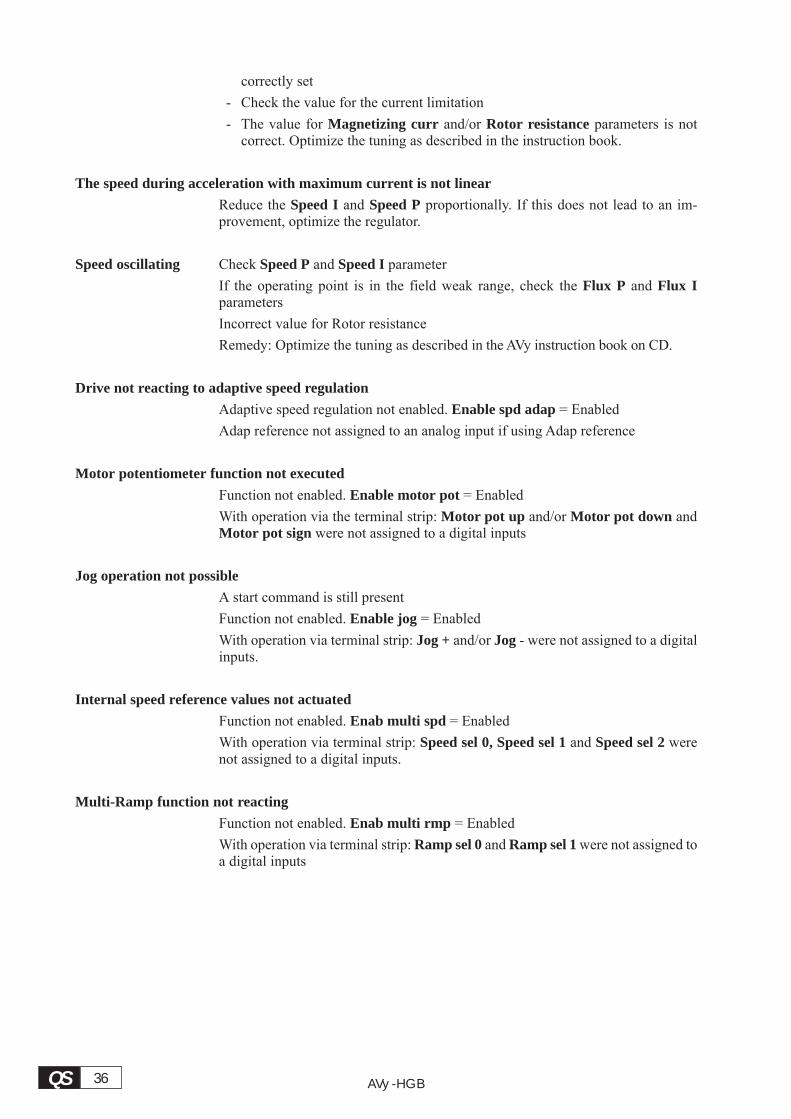
36QS AVy -HGB
correctly set
- Check the value for the current limitation
- The value for Magnetizing curr and/or Rotor resistance parameters is notcorrect. Optimize the tuning as described in the instruction book.
The speed during acceleration with maximum current is not linear
Reduce the Speed I and Speed P proportionally. If this does not lead to an im-provement, optimize the regulator.
Speed oscillating Check Speed P and Speed I parameter
If the operating point is in the field weak range, check the Flux P and Flux Iparameters
Incorrect value for Rotor resistance
Remedy: Optimize the tuning as described in the AVy instruction book on CD.
Drive not reacting to adaptive speed regulation
Adaptive speed regulation not enabled. Enable spd adap = Enabled
Adap reference not assigned to an analog input if using Adap reference
Motor potentiometer function not executed
Function not enabled. Enable motor pot = Enabled
With operation via the terminal strip: Motor pot up and/or Motor pot down andMotor pot sign were not assigned to a digital inputs
Jog operation not possible
A start command is still present
Function not enabled. Enable jog = Enabled
With operation via terminal strip: Jog + and/or Jog - were not assigned to a digitalinputs.
Internal speed reference values not actuated
Function not enabled. Enab multi spd = Enabled
With operation via terminal strip: Speed sel 0, Speed sel 1 and Speed sel 2 werenot assigned to a digital inputs.
Multi-Ramp function not reacting
Function not enabled. Enab multi rmp = Enabled
With operation via terminal strip: Ramp sel 0 and Ramp sel 1 were not assigned toa digital inputs
Ch.237—————— Function and feature (overview) ——————
2. FUNCTION AND FEATURE(OVERVIEW)
The AVy is a field-oriented vector Drive with excel-lent speed control properties and a high torque.
Available control modes are:- Field oriented with speed sensor- Field oriented without speed sensor (Sensorless
vect mode)- V/f control
Space vector modulation keeps the noise level to aminimum.- Output voltage up to 98% of input voltage- Self tuning procedure for current, flux and speed
regulators
The Drives are fitted with IGBTs (insulated gatebipolar transistors).
The output is protected against ground fault and phaseto phase output short.
Regulator power supply via switched-mode powersupply unit from the DC Bus circuit. Power supplybackup in the event of short-term voltage dips.
Galvanic isolation between control section andcommand terminals.
Analog inputs designed as differential inputs.
Simple operation of the drive- via the terminal strip- via the user-friendly keypad- via the PC program supplied and the RS485 serial
interface- via a fieldbus connection (optional): DeviceNet,
PROFIBUS-DP or GENIUS.- Easy Drive configuration tool
Fault register storing the last ten fault alarms withthe associated lifetime.Overload control.Engaging a running motor (Fly catching).Three freely configurable analog inputs on the stand-ard device.Expansion of the analog / digital outputs and analog/ digital inputs via option cards (EXP D8R4, EXPD14A4F).Reference value entry and actual value display as apercentage of a user-defined dimension.Speed and torque current regulation possible.Adaptive speed regulation.Speed-related alarms
Motor potentiometer function (Increase/Decreasespeed by command)Jog operation8 internal speed reference values (Preset speed)4 internal ramps
PID control
Controlled stop in case of AC mains power loss.

——— Function and feature (overview) ———Ch.2 38
Ch.339——— Inspection procedure, component identification and standard specification ———
3. INSPECTION PROCEDURE, COMPONENT IDENTIFICATIONAND STANDARD SPECIFICATION
3.1. UPON DELIVERY INSPECTION PROCEDURES
3.1.1. General
A high degree of care is taken in packing the AVy Drives and preparing them for delivery. They should onlybe transported with suitable transport equipment (see weight data). Observe the instructions printed on thepackaging. This also applies when the device is unpacked and installed in the control cabinet.
Upon delivery, check the following:
- the packaging for any external damage
- whether the delivery note matches your order.
Open the packaging with suitable tools. Check whether:
- any parts were damaged during transport
- the device type corresponds to your order
In the event of any damage or of an incomplete or incorrect delivery please notify the responsible salesofffices immediately.
The devices should only be stored in dry rooms within the specified temperature ranges .
NOTE! A certain degree of moisture condensation is permissible if this arises from changes intemperature (see section 3.4.1, “Permissible Environmental Conditions”). This does not,however, apply when the devices are in operation. Always ensure that there is no mois-ture condensation in devices that are connected to the power supply!
3.1.2. Inverter type designation
The technical specification of the AVy Drive is stated in the type code. Example:
X = software,standard L = LIFT software (specific for lift control)
X = without internal brake transistor , B = with internal brake transistor
X = KCS led module, K = programmable KBS keypad
Nominal motor output = 3kW
Enclosure dimension identification
Siei - AVy series vectorDrive , AC flux drive, 3 phase input voltage
AVy1030-XXX
The AVy Drive selected depends on the rated current of the motor. The rated output current at the appropri-ate service conditions must be greater than or equal to the motor current required.
The speed of the three-phase motor is determined by the number of pole pairs and the frequency (nameplate,data sheet) of the motor concerned. Operation above the rated frequency and speed of the motor must takeinto account the specifications given by the manufacturer losses (bearings, unbalance etc.). This also appliesto temperature specifications for continuous operation under 20 Hz (poor motor ventilation, not applicableto motors with external ventilation).
AVy - HGBCh.3 40
3.1.3. Nameplate
Check that all the data stated in the nameplate enclosed to the inverter correspond to what has been ordered.
Figure 3.1.3.1: Identification nameplate
Type : AVy1030-XXX S/N 9862330
Main Power In : 480 Vac 8.9 A 50/60Hz 3Phase
Main Power Out : 0-480Vac 7.5A 0-400Hz
LISTED
INDUSTRIAL CONTROL EQUIPMENT
Type: Inverter model S/N: Serial numberMain Power In: Power supply voltage - AC Input current - FrequencyMain Power Out: Output voltage - Output current - Output frequency
Figure 3.1.3.2: Firmware & Card revision level nameplate
Firmware HW release S/N 9862330 Prod.
Release D F P R S BU SW. CFG CONF
1.000 0.A 0.A 0.A 1.000 D1
Figure 3.1.3.3: Nameplates position
Ch.341——— Inspection procedure, component identification and standard specification ———
3.2. COMPONENT IDENTIFICATION
An AVy Drive converts the constant voltage and frequency of a three-phase power supply into a directvoltage and then converts this direct voltage into a new three-phase power supply with a variable voltageand frequency. This variable three-phase power supply can be used for the infinitely variable adjustment ofthe speed of three-phase asynchronous motors.
Figure 3.2.1: Basic Setup of Frequency Inverter
1 AC Input supply voltage
2 AC Mains choke (see section 5.7.1)
3 Three-phase rectifier bridge Converts the alternating current into direct current using a
three phase full wave bridge.
4 DC intermediate circuit With charging resistor and smoothing capacitor.
Direct voltage (UDC
) = √2 x Mains voltage (ULN
)
5 IGBT inverter Converts direct voltage to a variable three-phase alternating
voltage with variable frequency.
6 Configurable control section Modules for open-loop and closed-loop control of the
power section. This is used for processing control
commands, reference values and actual values.
7 Output voltage: Three-phase, variable alternating voltage.
8 Encoder For speed feedback (see section 4.4.2).
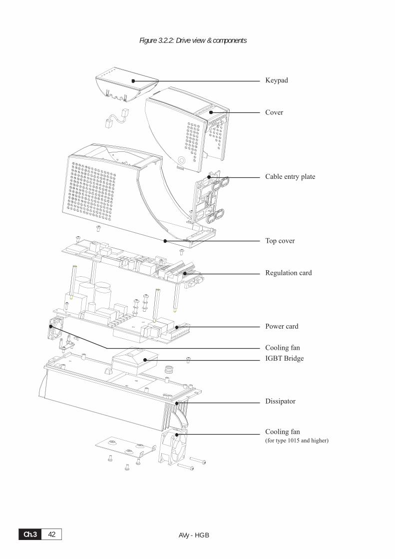
AVy - HGBCh.3 42
Figure 3.2.2: Drive view & components
Keypad
Cover
Cable entry plate
Top cover
Regulation card
Power card
Cooling fan
IGBT Bridge
Dissipator
Cooling fan(for type 1015 and higher)
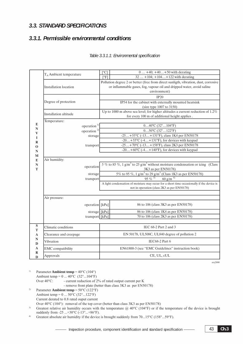
Ch.343——— Inspection procedure, component identification and standard specification ———
3.3. STANDARD SPECIFICATIONS
3.3.1. Permissible environmental conditions
Table 3.3.1.1: Environmental specification
[°C]
[°F]
Installation location
Installation altitude
Temperature:
operation 1)
operation 2)
storage
transport
Air humidity:
operation
storage
transport
Air pressure:
operation [kPa]
storage [kPa]
transport [kPa]
Climatic conditions
Clearance and creepage
Vibration
EMC compatibility
Approvals
TA Ambient temperature
E
N
V
I
R
O
N
M
E
N
T
IP54 for the cabinet with externally mounted heatsink
(size type 1007 to 3150)
IP20
Degree of protection
86 to 106 (class 3K3 as per EN50178)
86 to 106 (class 1K4 as per EN50178)
-25…+55°C (-13…+131°F), class 1K4 per EN50178
-20…+55°C (-4…+131°F), for devices with keypad
-25…+70°C (-13…+158°F), class 2K3 per EN50178
-20…+60°C (-4…+140°F), for devices with keypad
Up to 1000 m above sea level; for higher altitudes a current reduction of 1.2%
for every 100 m of additional height applies .
0…40°C (32°…104°F)
0…50°C (32°…122°F)
0 … +40; +40…+50 with derating
32 … +104; +104…+122 with derating
Pollution degree 2 or better (free from direct sunligth, vibration, dust, corrosive
or inflammable gases, fog, vapour oil and dripped water, avoid saline
environment)
70 to 106 (class 2K3 as per EN50178)
IEC 68-2 Part 2 and 3
EN 50178, UL508C, UL840 degree of pollution 2
IEC68-2 Part 6
EN61800-3 (see “EMC Guidelines” instruction book)
CE, UL, cUL
avy2000
S
T
A
N
D
A
R
D
5% to 95 %, 1 g/m3 to 29 g/m3 (Class 1K3 as per EN50178)
5 % to 85 %, 1 g/m3 to 25 g/m3 without moisture condensation or icing (Class
3K3 as per EN50178)
95 % 3) 60 g/m 4)
A light condensation of moisture may occur for a short time occasionally if the device is
not in operation (class 2K3 as per EN50178)
1) Parameter Ambient temp = 40°C (104°)Ambient temp = 0 ... 40°C (32°...104°F)Over 40°C: - current reduction of 2% of rated output current per K
- remove front plate (better than class 3K3 as per EN50178)2) Parameter Ambient temp = 50°C (122°F)
Ambient temp = 0 ... 50°C (32°...122°F)Current derated to 0.8 rated ouput currentOver 40°C (104°): removal of the top cover (better than class 3K3 as per EN50178)
3) Greatest relative air humidity occurs with the temperature @ 40°C (104°F) or if the temperature of the device is broughtsuddenly from -25 ...+30°C (-13°...+86°F).
4) Greatest absolute air humidity if the device is brought suddenly from 70...15°C (158°...59°F).
AVy - HGBCh.3 44
Disposal of the Device
The AVy Drive can be disposed as electronic scraps in accordance with the currently valid national regula-tions for the disposal of electronic parts.
The plastic covering of the Drives (up to size 3150) are recyclable: the material used is >ABS+PC< .
3.3.2. AC Input/Output Connection
The AVy Drive must be connected to an AC mains supply capable of delivering a symmetrical short circuitcurrent (at 480V +10% Vmax) lower or equal to the values indicated on following table. For the use of anAC input choke see chapter 5.7.1.
No external connection of the regulator power supply to the existing AC Input supply is required since thepower supply is taken from the DC Link circuit. When commissioning, set the Mains voltage parameter tothe value of the AC Input voltage concerned. This automatically sets the threshold for the Undervoltagealarm at the appropriate level.
NOTE! In some cases AC Input chokes, and possibly noise suppression filters should be fittedon the AC Input side of the device. See chapter “Chokes/Filters”.
Adjustable Frequency Drives and AC Input filters have ground discharge currents greater then 3.5 mA. EN50178 specifies that with discharge currents greater than 3.5 mA the protective conductor ground connection(PE1) must be fixed type.
AVy...-DC versions
In this version, the drive must be powered by a rectified DC supply of 600 Vdc.
The use of Gefran SM32 series power supplies is recommended for this, available with an output currentfrom 185 to 2000A.
From size AVy4185, insertion of an AC mains inductance on the power supply input of the power supplyunit is compulsory (for the type of inductance, consult the manual of the power supply unit), see figure
5.5.1.2.
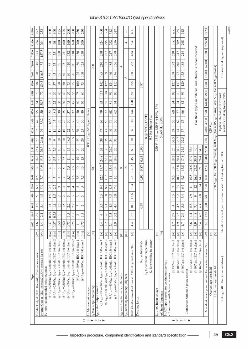
Ch.345——— Inspection procedure, component identification and standard specification ———
Table 3.3.2.1:AC Input/Output specifications
10
07
10
15
10
22
10
30
20
40
20
55
20
75
31
10
31
50
41
85
42
20
43
00
43
70
54
50
55
50
67
50
79
00
71
10
07
13
20
81
60
08
20
00
Inve
rter
Ou
tpu
t(I
EC
146
clas
s1),
Co
nti
nu
ou
sse
rvic
e[k
VA
]1.
62.
73.
85
6.5
8.5
1216
.822
.427
3242
5564
7998
128
145
173
224
277
Inve
rter
Ou
tpu
t(I
EC
146
clas
s2),
150%
ove
rlo
adfo
r60
s[k
VA
]1.
42.
43.
44.
55.
97.
710
.915
.320
.324
.629
38.2
5058
.372
89.2
116.
513
215
7.5
204
252
PN
mo
t(r
eco
mm
end
edm
oto
ro
utp
ut)
:
@U
LN
=23
0Vac
;f S
W=
def
ault
;IE
C14
6cl
ass
1[k
W]
0.37
0.75
1.1
1.5
2.2
34
5.5
7.5
1011
18.5
2222
3037
5555
7590
100
@U
LN
=23
0Vac
;f S
W=
def
ault
;IE
C14
6cl
ass
2[k
W]
0.37
0.75
1.1
1.5
2.2
34
5.5
7.5
911
1518
.522
3037
4555
5590
100
@U
LN
=23
0Vac
;f S
W=
def
ault
;IE
C14
6cl
ass
1[H
p]
0.50
11.
52
34
57.
510
1015
2530
3040
5075
7510
010
012
5
@U
LN
=23
0Vac
;f S
W=
def
ault
;IE
C14
6cl
ass
2[H
p]
0.50
11.
52
34
57.
510
1015
2025
3040
5060
7575
100
125
@U
LN
=40
0Vac
;f S
W=
def
ault
;IE
C14
6cl
ass
1[k
W]
0.75
1.5
2.2
34
5.5
7.5
1115
18.5
2230
3745
5575
9011
013
216
020
0
@U
LN
=40
0Vac
;f S
W=
def
ault
;IE
C14
6cl
ass
2[k
W]
0.75
1.5
2.2
34
5.5
7.5
1115
18.5
2230
3745
5555
9090
110
160
200
@U
LN
=46
0Vac
;IE
C14
6cl
ass
1[H
p]
12
33
57.
510
1520
2530
4050
6075
100
125
150
150
200
250
@U
LN
=46
0Vac
;IE
C14
6cl
ass
2[H
p]
0.75
1.5
23
57.
510
1520
2025
3040
5060
7510
012
515
020
025
0
U2
Max
ou
tpu
tvo
ltag
e[V
]
f 2M
axo
utp
ut
freq
uen
cy[H
z]
I 2N
Rat
edo
utp
ut
curr
ent
:
@U
LN
=23
0-40
0Vac
;f S
W=
def
ault
;IE
C14
6cl
ass
1[A
]2.
44
5.6
7.5
9.6
12.6
17.7
24.8
3339
4763
7993
114
142
185
210
250
324
400
@U
LN
=23
0-40
0Vac
;f S
W=
def
ault
;IE
C14
6cl
ass
2[A
]2.
23.
65.
16.
88.
711
.516
.122
.530
3543
5872
8510
412
916
919
122
729
536
4
@U
LN
=46
0Vac
;f S
W=
def
ault
;IE
C14
6cl
ass
1[A
]2.
13.
54.
96.
58.
311
15.4
21.6
28.7
3440
5468
8199
124
160
183
217
282
348
@U
LN
=46
0Vac
;f S
W=
def
ault
;IE
C14
6cl
ass
2[A
]1.
93.
24.
45.
97.
610
1419
.626
3136
5062
7490
112
146
166
198
256
317
f SW
swit
chin
gfr
equ
ency
(Def
ault
)[k
Hz]
f SW
swit
chin
gfr
equ
ency
(Hig
her
)[k
Hz]
4--
Iovl
d(s
ho
rtte
rmo
verl
oad
curr
ent,
200%
of
I 2N
for
0.5s
on
60s)
[A]
4.4
7.2
10.2
13.6
17.4
2332
.245
6070
8611
614
417
020
825
833
838
245
4n
.a.
n.a
.
Der
atin
gfa
cto
r:
KV
at46
0/48
0Vac
0.96
0.87
0.93
0.90
KT
for
amb
ien
tte
mp
erat
ure
KF
for
swit
chin
gfr
equ
ency
UL
NA
CIn
pu
tvo
ltag
e[V
]
AC
Inp
ut
freq
uen
cy[H
z]
I NA
CIn
pu
tcu
rren
tfo
rco
nti
nu
ou
sse
rvic
e:
-C
on
nec
tio
nw
ith
3-p
has
ere
acto
r @23
0Vac
;IE
C14
6cl
ass1
[A]
1.7
2.9
45.
57
9.5
1418
.225
32.5
3955
6984
9812
215
819
222
0n
.a.
n.a
.
@40
0Vac
;IE
C14
6cl
ass1
[A]
1.9
3.3
4.5
6.2
7.9
10.7
15.8
20.4
28.2
36.7
4462
7794
110
137
177
216
247
309
365
@46
0Vac
;IE
C14
6cl
ass1
[A]
1.7
2.9
3.9
5.4
6.7
9.3
13.8
17.8
24.5
32.5
3753
6682
9612
015
318
821
426
831
8-
Co
nn
ecti
on
wit
ho
ut
3-p
has
ere
acto
r
@23
0Vac
;IE
C14
6cl
ass1
[A]
3.6
4.4
6.8
7.9
1115
.521
.527
.935
.4
@40
0Vac
;IE
C14
6cl
ass1
[A]
3.9
4.8
7.4
912
16.9
24.2
30.3
40
@46
0Vac
;IE
C14
6cl
ass1
[A]
3.4
4.2
6.4
7.8
10.4
14.7
2126
.434
.8
Max
sho
rtci
rcu
itp
ow
erw
ith
ou
tli
ne
reac
tor
(Zm
in=
1%)
[kV
A]
160
270
380
500
650
850
1200
1700
2250
2700
3200
4200
5500
6400
7900
9800
1280
014
500
1730
022
400
2770
0
[V]
[V]
avy2
010
16
0.87
0.8
@50
°C(1
22°F
)
0.7
for
hig
her
f SW
200
Bra
kin
gIG
BT
Un
it(s
tan
dar
dd
rive
)
O U T P U T I N P U T
Ove
rvo
ltag
eth
resh
old
Un
der
volt
age
thre
sho
ld
230
V-1
5%...
480
V+
10%
,3P
h
230
VD
C(f
or
230
VA
Cm
ain
s),4
00V
DC
(fo
r40
0VA
Cm
ain
s),4
60V
DC
for
460
VA
Cm
ain
s)
Typ
e
0.87
8
4
0.98
xU
LN
(AC
Inp
ut
volt
age)
500 8
Ext
ern
alb
rak
ing
un
it(o
pti
on
al)
50/6
0H
z±
5%
820
VD
C
Sta
nd
ard
inte
rnal
(wit
hex
tern
alre
sist
or)
;B
rak
ing
torq
ue
150%
Op
tio
nin
tern
al(w
ith
exte
rnal
resi
sto
r);
Bra
kin
gto
rqu
e15
0%
Fo
rth
ese
typ
esan
exte
rnal
ind
uct
ance
isre
com
men
ded
AVy - HGBCh.3 46
3.3.3. AC Input current
NOTE! The Input current of the Drive depends on the operating state and the service conditionsof the connected motor, and the use of input reactors. The table 3.3.2.1 shows the valuescorresponding to rated continuous service (IEC 146 class 1), keeping into account typicaloutput power factor for each size
3.3.4. AC Output
The output of the AVy Drive is ground fault and phase to phase output short protected. The switchingfrequency is constant in the speed range and depends on the drive size.
NOTE! The connection of an external voltage to the output terminals of the Drive is not permissible!It is allowed to disconnect the motor from the Drive output, after the Drive has been disabled.
The value for the continuous output current rating ( ICONT
) depends on AC Input voltage ( KV ), Ambient
temperature ( KT ) and Switching frequency ( K
F ):
ICONT
= I2N
x KV x K
T x K
F (Values of derating factor are the listed on table 3.3.2.1)
with an overload capacity IMAX
= 1.36 x ICONT
for 60 seconds
The applicable deratings are automatically set when selecting the appropriate values of AC Input voltage,Ambient temperature and Switching frequency.
Recommended motor outputs
The coordination of the motor rated powers with the Drive type presented in the table below refers to the useof standard 4 poles motors with a rated voltage equal to the rated voltage of the input supply.
As for those motors with different voltages, the type of Drive to use is determined by the rated current of themotor.
Motor nominal current cannot be lower than 0,3 x I2N
. Magnetizing motor current must not be higher ofI
CONT.
NOTE! For service conditions with overload higher than 150%, the nominal current must bederated.
Table 3.3.3.1 shows nominal current values for typical service profiles (Ambienttemperature =40°C [104°F], standard switching frequency). For cycles with nominalcurrent applied after the overload, the minimum duration is also specified.
For cycles shorter than the minimum duration specified, the current following the overloadshould be reduced to a level lower than the nominal, so that the RMS average over thecycle does not exceed the continuous current, I
CONT.
Similar criteria apply for operation with additional derating factors.
Ch.347——— Inspection procedure, component identification and standard specification ———
Table 3.3.3.1: Nominal Drive Current
10
07
10
15
10
22
10
30
20
40
20
55
20
75
31
10
31
50
41
85
42
20
43
00
43
70
54
50
55
50
67
50
79
00
71
10
07
13
20
81
60
08
20
00
Co
nti
nu
ou
sse
rvic
e,n
oo
verl
oad
(IE
C14
6cl
ass
1)[A
]2.
44
5.6
7.5
9.6
12.6
17.7
24.8
3339
4763
7993
114
142
185
210
250
324
400
Ove
rlo
adse
rvic
e15
0%x6
0sfo
llo
wed
by
I N,m
in.c
ycle
tim
e36
0s
(IE
C14
6cl
ass2
)[A
]2.
23.
65.
16.
88.
711
.516
.122
.529
.935
4357
7285
104
129
168
191
228
295
364
Ove
rlo
adse
rvic
e20
0%x1
0sfo
llo
wed
by
I N,m
in.c
ycle
tim
e30
s[A
]1.
62.
73.
85.
16.
58.
612
.016
.922
.427
3243
5463
7897
126
143
171
221
273
Ove
rlo
adse
rvic
e20
0%x6
0sfo
llo
wed
by
I N,m
in.c
ycle
tim
e16
0s[A
]1.
62.
73.
85.
16.
58.
612
.016
.922
.427
3243
5463
7897
126
143
171
221
273
Ove
rlo
adse
rvic
e25
0%x1
0sfo
llo
wed
by
I N,m
in.c
ycle
tim
e25
s[A
]1.
32.
23.
04.
15.
26.
89.
613
.518
2126
3443
5162
7810
111
513
717
721
8
Ove
rlo
adse
rvic
e30
0%x1
0sfo
llo
wed
by
I N,m
in.c
ycle
tim
e25
s[A
]1.
11.
82.
53.
44.
35.
78.
011
.215
1821
2936
4252
6584
9611
414
718
2
Ove
rlo
adse
rvic
e30
0%x6
0sfo
llo
wed
by
I N,m
in.c
ycle
tim
e13
0s[A
]1.
11.
82.
53.
44.
35.
78.
011
.215
1821
2936
4252
6584
9611
414
718
2
Co
nti
nu
ou
sse
rvic
e,n
oo
verl
oad
(IE
C14
6cl
ass
1)[A
]2.
13.
54.
96.
58.
311
15.4
21.6
28.7
3441
5569
8199
124
161
183
218
282
348
Ove
rlo
adse
rvic
e15
0%x6
0sfo
llo
wed
by
I N,m
in.c
ycle
tim
e36
0s
(IE
C14
6cl
ass2
)[A
]1.
93.
24.
45.
97.
610
1419
.626
3137
5063
7490
112
146
166
198
257
317
Ove
rlo
adse
rvic
e20
0%x1
0sfo
llo
wed
by
I N,m
in.c
ycle
tim
e30
s[A
]1.
42.
43.
34.
45.
67.
510
.514
.719
.523
2837
4755
6884
110
125
148
192
238
Ove
rlo
adse
rvic
e20
0%x6
0sfo
llo
wed
by
I N,m
in.c
ycle
tim
e16
0s[A
]1.
42.
43.
34.
45.
67.
510
.514
.719
.523
2837
4755
6884
110
125
148
192
238
Ove
rlo
adse
rvic
e25
0%x1
0sfo
llo
wed
by
I N,m
in.c
ycle
tim
e25
s[A
]1.
11.
92.
73.
54.
56.
08.
411
.715
.619
2230
3844
5467
8810
011
915
419
0
Ove
rlo
adse
rvic
e30
0%x1
0sfo
llo
wed
by
I N,m
in.c
ycle
tim
e25
s[A
]0.
91.
62.
22.
93.
85.
07.
09.
813
1519
2531
3745
5673
8399
128
158
Ove
rlo
adse
rvic
e30
0%x6
0sfo
llo
wed
by
I N,m
in.c
ycle
tim
e13
0s[A
]0.
91.
62.
22.
93.
85.
07.
09.
813
1519
2531
3745
5673
8399
128
158
avy2
020
-I 2
NR
ate
do
utp
ut
curr
ent
(@U
LN=
230-4
00V
ac)
:
-I 2
Nx
KV
Ra
ted
ou
tpu
tcu
rren
t(@
UL
N=
460/4
80V
ac)
:
Typ
e
AVy - HGBCh.3 48
3.3.5. Open-Loop and Closed-Loop Control Section
Enable inputs 0 / 15...30 V 3.2...6.4 mA (5 mA @ 24 V)
Analog inputs Selectable 0... ± 10 V 0.25 mA max0...20 mA 10 V max4...20 mA 10 V max
Max common mode voltage: 0...± 10 V
Analog outputs 0...± 10 V 5 mA max per output
Digital inputs 0 / 15...30 V 3.2...6.4 mA (5 mA @ 24 V)
Digital outputs Supply + 15...35 VSignals + 15...35 V 40 mA max per output
Encoder inputs Sinusoidal Voltage 1 V pp
Current 8.3 mA pp per channel (input resistance = 124 Ohms).No. of pulses min 600per revolution max 9999max. frequency 80 kHzCable max. 500 feet (150 m), screened, 4 twisted pairs as shown in the table 4.4.2.1
Digital Voltage 5 VCurrent 10 mANo. of pulses min 600per revolution max 9999Type standard and inverted signalmax. frequency 150 kHz
Int. voltage supply
Load capacity + 5 V 160 mA Plug connector+ 10 V 10 mA Terminal 7- 10 V 10 mA Terminal 8+ 24 V 120 mA Terminal 19
Tolerance + 10 V ± 3 % 1)
- 10 V ± 3 % 1)
+ 24 V + 20 ... 30 V, not stabilized
XE for digital encoder, PIN 7/9
1) The tolerance between positive and negative amplitudes is ± 0.5%
Ch.349——— Inspection procedure, component identification and standard specification ———
3.3.6. Accuracy
[°C]
[V]
[°C]
Speed limit / Absolute max speed [rpm]
Digital reference resolution [rpm]
Field oriented (with sinusoidal Encoder):
accuracy [%]
control range [rpm]
max bandwidth [rad/s]
Field oriented (with digital Encoder):
speed feedback resolution [rpm]
accuracy [%]
control range [rpm]
max bandwidth [rad/s]
Sensorless vector control:
speed feedback resolution [rpm]
control range [rpm]
max bandwidth [rad/s]
Constant V/f control:
accuracy [rpm]
control range [%]
Field oriented - Sensorless:
resolution [rpm]
accuracy [%]
control range [rpm]
min. response time (at load step) [ms]
max bandwidth
[rpm]
300 rad/s [47 Hz] (1)
> 0.25(for encoder pulses number <1900)
300 rad/s [47 Hz] (1)
0.25 (for encoder pulses number � 1900)
typical 0.01%
better than 1:10000
16 bit or 15 bit + sign
linearity via terminals ( 1/2, 3/4, 5/6 )
- temperature dependent stability error 100 ppm/°C typical
Reference values:
11 bit + sign
± 0.1 % of full scale
avy2030
resolution via keypad / Interface bus
resolution via terminals ( 1/2, 3/4, 5/6 )
8000
0.25
S
P
E
E
D
C
O
N
T
R
O
L
1.3% @ 2% of Nominal speedaccuracy [%]
speed feedback resolution
� 50 ppm/°C typicaltemperature dependent stability error
Internal reference value voltage:
Output frequency:
0.001 Hz at 50 Hz
± 10V, terminals 7 and 8
0.005 Hz at 300 Hzresolution [Hz]
0.5
typical 0.02%
better than 1:1000
0.002 x Nominal speed
0.3% @ Nominal speed
from 1:50 to 2.5 x Nominal speed
T
O
R
Q
U
E
C
O
N
T
R
O
L
typical 1:1.000
typical 5% (2)
1÷20
0.8
2.4 krad/s [380 Hz]
depending on motor nominal slip, typ. 1:50
100 rad /s [15,9Hz] (1)
0.3 x nominal motor slip with automatic slip
compensation
(1) The response time and bandwidth are affected by the load and inertia. These represent limit values.(2) This value does not include iron losses, mechanical losses and cogging torque. With Rr adaptation enabled.

AVy - HGBCh.3 50
Ch.451—————— Installation guidelines ——————
4. INSTALLATION GUIDELINES
4.1. MECHANICAL SPECIFICATION
Figure 4.1.1: Drive dimensions (sizes 1007 ... 3150)
Figure 4.1.2: Mounting methods (sizes 1007 ... 3150)
Mounting wall (D)Mounting with external dissipator (E)
E2 E4
E5
E3
E1
d
Table 4.1.1: Drive dimensions and Weights (sizes 1007 ... 3150)
1007 1015 1022 1030 2040 2055 2075 3110 3150
a mm (inch)
b mm (inch)
c mm (inch)
d mm (inch)
D1 mm (inch)
D2 mm (inch)
E1 mm (inch)
E2 mm (inch)
E3 mm (inch)
E4 mm (inch)
E5 mm (inch)
Ø d
Weight kg (lbs) 3.5 (7.7) 3.6 (7.9)avy3100
8.6 (19)3.7 (8.1) 4.95 (10.9)
M5
Type
306.5 (12.0)
105.5 (4.1) 151.5 (5.9)
Drive dimensions:
310.5 (12.2)
164 (6.5)
296.5 (11.6)
299.5 (11.7)
69 (2.7)
315 (12.4)
208 (8.2)
323 (12.7)
240 (9.5)
168 (6.6)
84 (3.3)
115 (4.5)
115 (4.5)
199.5 (7.8)
69 (2.7)
62 (2.4)
9 (0.35)
299.5 (11.8)
99.5 (3.9) 145.5 (5.7) 199 (7.8)
284 (11.2)

AVy - HGBCh.4 52
Figure 4.1.3: Drive dimensions (sizes 4185 ... 82000)
Figure 4.1.4: Mounting methods (sizes 4185 ... 82000)
D1
D2 D2
D3 D3 D3 D3
D4
Mounting wall (D)
Table 4.1.2: Drive dimensions and Weights (sizes 4185 ... 82000)
4185 4220 4300 4370 5450 5550 6750 7900 71100 71320 81600 82000
a mm (inch)
b mm (inch) 741 (29.2)
c mm (inch)
D1 mm (inch)
D2 mm (inch)
D3 mm (inch)
D4 mm (inch) 725 (28.5)
Ø
Weight kg 22 22.2 34 34 59 75.4 80.2 86.5
lbs 48.5 48.9 74.9 74.9 130 166.1 176.7 190.6
avy3105
M6
268 (10.5)
225 (8.8)
475 (18.7)
Type
150 (5.9)
550 (21.6)
100 (3.9)
308 (12.1) 297.5 (11.7)
Drive dimensions:
509 (20)
564 (22.2)
376 (14.7)
909 (35.8)
309 (12.1)
489 (19.2)
18
39.6
965 (38)
442 (17.4)
947 (37.3)
109
240.3
891 (35)
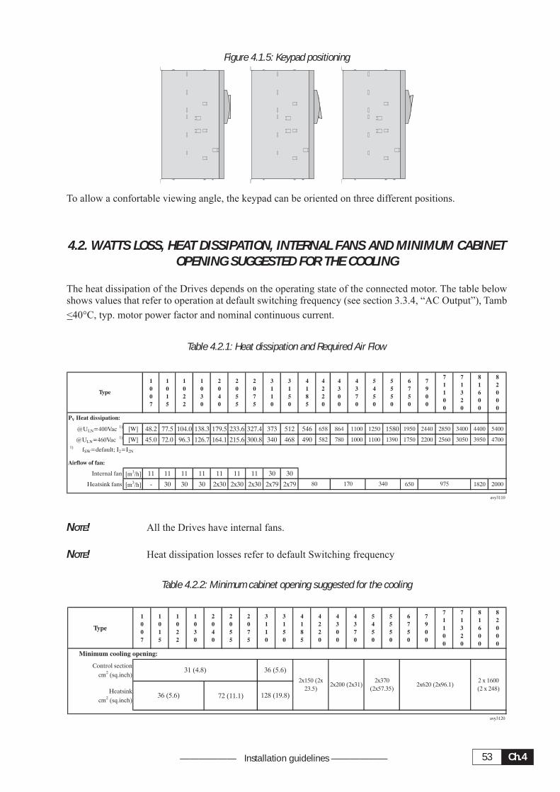
Ch.453—————— Installation guidelines ——————
Figure 4.1.5: Keypad positioning
To allow a confortable viewing angle, the keypad can be oriented on three different positions.
4.2. WATTS LOSS, HEAT DISSIPATION, INTERNAL FANS AND MINIMUM CABINETOPENING SUGGESTED FOR THE COOLING
The heat dissipation of the Drives depends on the operating state of the connected motor. The table belowshows values that refer to operation at default switching frequency (see section 3.3.4, “AC Output”), Tamb
<40°C, typ. motor power factor and nominal continuous current.
Table 4.2.1: Heat dissipation and Required Air Flow
1
0
0
7
1
0
1
5
1
0
2
2
1
0
3
0
2
0
4
0
2
0
5
5
2
0
7
5
3
1
1
0
3
1
5
0
4
1
8
5
4
2
2
0
4
3
0
0
4
3
7
0
5
4
5
0
5
5
5
0
6
7
5
0
7
9
0
0
7
1
1
0
0
7
1
3
2
0
8
1
6
0
0
8
2
0
0
0
PV Heat dissipation:
@ULN=400Vac 1) [W] 48.2 77.5 104.0 138.3 179.5 233.6 327.4 373 512 546 658 864 1100 1250 1580 1950 2440 2850 3400 4400 5400
@ULN=460Vac 1) [W] 45.0 72.0 96.3 126.7 164.1 215.6 300.8 340 468 490 582 780 1000 1100 1390 1750 2200 2560 3050 3950 47001) fSW=default; I2=I2N
Airflow of fan:
Internal fan [m3/h] 11 11 11 11 11 11 11 30 30
Heatsink fans [m3/h] - 30 30 30 2x30 2x30 2x30 2x79 2x79 650 1820 2000
avy3110
Type
170 340 97580
NOTE! All the Drives have internal fans.
NOTE! Heat dissipation losses refer to default Switching frequency
Table 4.2.2: Minimum cabinet opening suggested for the cooling
Type
1
0
0
7
1
0
1
5
1
0
2
2
1
0
3
0
2
0
4
0
2
0
5
5
2
0
7
5
3
1
1
0
3
1
5
0
4
1
8
5
4
2
2
0
4
3
0
0
4
3
7
0
5
4
5
0
5
5
5
0
6
7
5
0
7
9
0
0
7
1
1
0
0
7
1
3
2
0
8
1
6
0
0
8
2
0
0
0
Control section
cm2 (sq.inch)
Heatsink
cm2 (sq.inch)72 (11.1)
avy3120
Minimum cooling opening:
36 (5.6)
31 (4.8) 36 (5.6)
128 (19.8)
2x150 (2x
23.5)
2 x 1600
(2 x 248)2x200 (2x31)
2x370
(2x57.35)2x620 (2x96.1)
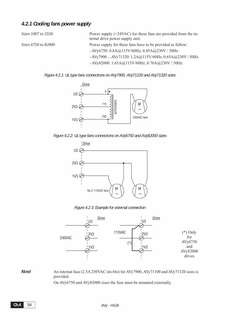
AVy - HGBCh.4 54
4.2.1 Cooling fans power supply
Sizes 1007 to 5550 Power supply (+24VAC) for these fans are provided from the in-ternal drive power supply unit.
Sizes 6750 to 82000 Power supply for these fans have to be provided as follow:
- AVy6750: 0.8A@115V/60Hz, 0.45A@230V / 50Hz
- AVy7900 ... AVy71320: 1.2A@115V/60Hz, 0.65A@230V / 50Hz
- AVy82000: 1.65A@115V/60Hz, 0.70A@230V / 50Hz
Figure 4.2.1: UL type fans connections on AVy7900, AVy71100 and AVy71320 sizes
M
~
U3
2V3
1V3
0
115
230A
UTO
TRA
FO230VAC fans
Drive
Figure 4.2.2: UL type fans connections on AVy6750 and AVy82000 sizes
M
~
U3
2V3
1V3
No.2 115VAC fansM
~
Drive
Figure 4.2.3: Example for external connection
U3
2V3
1V3
230VAC
U3
2V3
1V3
115VAC
Drive Drive
(*)
NOTE! An internal fuse (2.5A 250VAC slo-blo) for AVy7900, AVy71100 and AVy71320 sizes isprovided.
On AVy6750 and AVy82000 sizes the fuse must be mounted externally.
(*) Onlyfor
AVy6750and
AVy82000drives
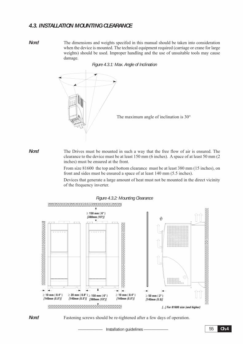
Ch.455—————— Installation guidelines ——————
4.3. INSTALLATION MOUNTING CLEARANCE
NOTE! The dimensions and weights specifed in this manual should be taken into considerationwhen the device is mounted. The technical equipment required (carriage or crane for largeweights) should be used. Improper handling and the use of unsuitable tools may causedamage.
Figure 4.3.1: Max. Angle of Inclination
The maximum angle of inclination is 30°
NOTE! The Drives must be mounted in such a way that the free flow of air is ensured. Theclearance to the device must be at least 150 mm (6 inches). A space of at least 50 mm (2inches) must be ensured at the front.
From size 81600 the top and bottom clearance must be at least 380 mm (15 inches), onfront and sides must be ensured a space of at least 140 mm (5.5 inches).
Devices that generate a large amount of heat must not be mounted in the direct vicinityof the frequency inverter.
Figure 4.3.2: Mounting Clearance
� 10 mm 0.4"( )
[140mm (5.5")]
� 6"150 mm ( )
[380mm (15")]
� 2" )50 mm (
[140mm (5.5)]
� 20 mm ( 0.8" )
[140mm (5.5")]� 6"150 mm ( )
[380mm (15")]
� 10 mm 0.4"( )
[140mm (5.5")]
[...] For 81600 size (and higher)
NOTE! Fastening screws should be re-tightened after a few days of operation.
AVy - HGBCh.4 56
4.4. MOTORS AND ENCODERS
The AVy Drives designed for the field oriented regulation of standard three-phase induction AC motors. Asinusoidal encoder or digital encoder can be used for feedback in proportion to speed.
4.4.1. Motors
The electrical and mechanical data of standard three-phase motors refers to a particular operating range. Thefollowing points should be noted when these motors are connected to an AC Drive:
Is it possible to use standard induction motors?
With the AVy Drives it is possible to use standard induction motors. Some features of the motor have a greatinfluence on the obtained performances. Notice also what is stated in section 3.3.4, “AC Output”, about thevoltages and the motor power.
Which properties of the asynchronous motors have an unfavorable result in operation with fre-quency inverters?
Motors with double squirrel-cage rotors or deep rotor bars should not be used.
Star or delta connection?
Motors can be connected in both star or delta connections. Experience has shown that star connected motorshave better control properties, so star connections are preferred.
Cooling
The cooling of three-phase motors is normally implemented by means of a fan that is mounted on the motorshaft. Remember that the output of the fan is reduced when the motor is running at lower speeds, which incertain circumstances may mean that the cooling is insufficient for the motor. Check with the motor manu-facturer whether an external fan is required and the motor speed range in the application concerned.
Operation above the rated speed
Due to the mechanical factors involved (bearings, unbalance of rotor) and due to the increased iron losses,consult the manufacturer of the motor if this is operated above the rated speed .
What motor data is required for connecting the frequency inverter?
Nameplate specifications
- Motor rated voltage
- Motor rated current
- Motor rated frequency
- Motor rated speed
- Power factor
The other data required for vector control is calculated inside the inverter. In order to optimize the driveoperation it is also useful to know the values for :
- Magnetizing current
- Rotor resistance
- Stator resistance (Sensorless mode only)
- Leakage inductance ( Field oriented mode with Rotor resistance adaptation enabled or Sensorless mode.).
Motor protection
Thermistors
PTC thermistors according to DIN 44081 or 44082 fitted in the motor can be connected directly to thefrequency inverter via terminals 78 and 79. In this case the resistor (1Kohm) mounted between the terminals78 and 79 has to be removed.
Ch.457—————— Installation guidelines ——————
Temperature-dependent contacts in the motor winding
Temperature-dependent contacts “Klixon” type can disconnect the drive via the external control or can bereported as an external fault on the frequency inverter (terminal 15). They can also be connected to theterminals 78 and 79 in order to have a specific error signal. In this case connect the existing 1 Kohm resistorin series to the wiring, note that one side of it must be connected directly to terminal 79.
NOTE! The motor PTC interface circuit (or klixon) has to be considered and treated as a signalcircuit. The connections cables to the motor PTC must be made of twisted pairs with ashield, the cable route should not be parallel to the motor cable or far away at least 20 cm.
Current limitation of the frequency inverter
The current limitation can protect the motor from impermissible overloads. For this the current limitationand the motor overload control function of the Drive (“Ovld mot ctrl”) must be set so that the current is keptwithin the permissible range for the motor concerned.
NOTE! Remember that the current limitation can control an overheating of the motor only dueto overload, not due to insufficient ventilation. When the drive is operated at low speedsthe additional use of PTC resistors or temperature-dependent contacts in the motorwindings is recommended, unless separate forced ventilation is available.
Output chokes
When using general purpose standard motors, output chokes are recommended to protect winding isolationin some cases. See section 5.7.2, “ Output chokes”.
4.4.2. Encoder
One of two types of encoder may be connected to the XE connector (high density 15-pole socket, fitted ondevice), see the table 4.4.2.2 for the jumper settings
- DE: 5V digital incremental encoder with A / A, B / B, C / C
- SE: 5V sinusoidal incremental encoder with A / A, B / B, C / C
Encoders are used to feed back a speed signal to the regulator. The encoder should be coupled to the motorshaft with a backlash free connection.
Optimal regulation results are ensured when using sinusoidal encoders. Digital encoders (rotary encoders)may also be used. See section 4.3.6, “Accuracy”.
The encoder cable can be made of twisted pairs with a global shield, which connect to ground on the Driveside. Avoid connecting the shield on the motor side. In particular cases where the cable length is more than100 meters (328 feet), (high electromagnetic noise), it may useful to use a cable with a shield on eachconductor pair, which can be connected to the common point (0V). The global shield must always be grounded.
Some types of sinusoidal encoders may require installation with galvanic isolation from the motor frameand shaft.
Table 4.4.2.1: Recommended cable section and length for the connection of encoders
Cable section [mm2] 0.22 0.5 0.75 1 1.5
Max Length m [feet] 27 [88] 62 [203] 93 [305] 125 [410] 150 [492]avy3130
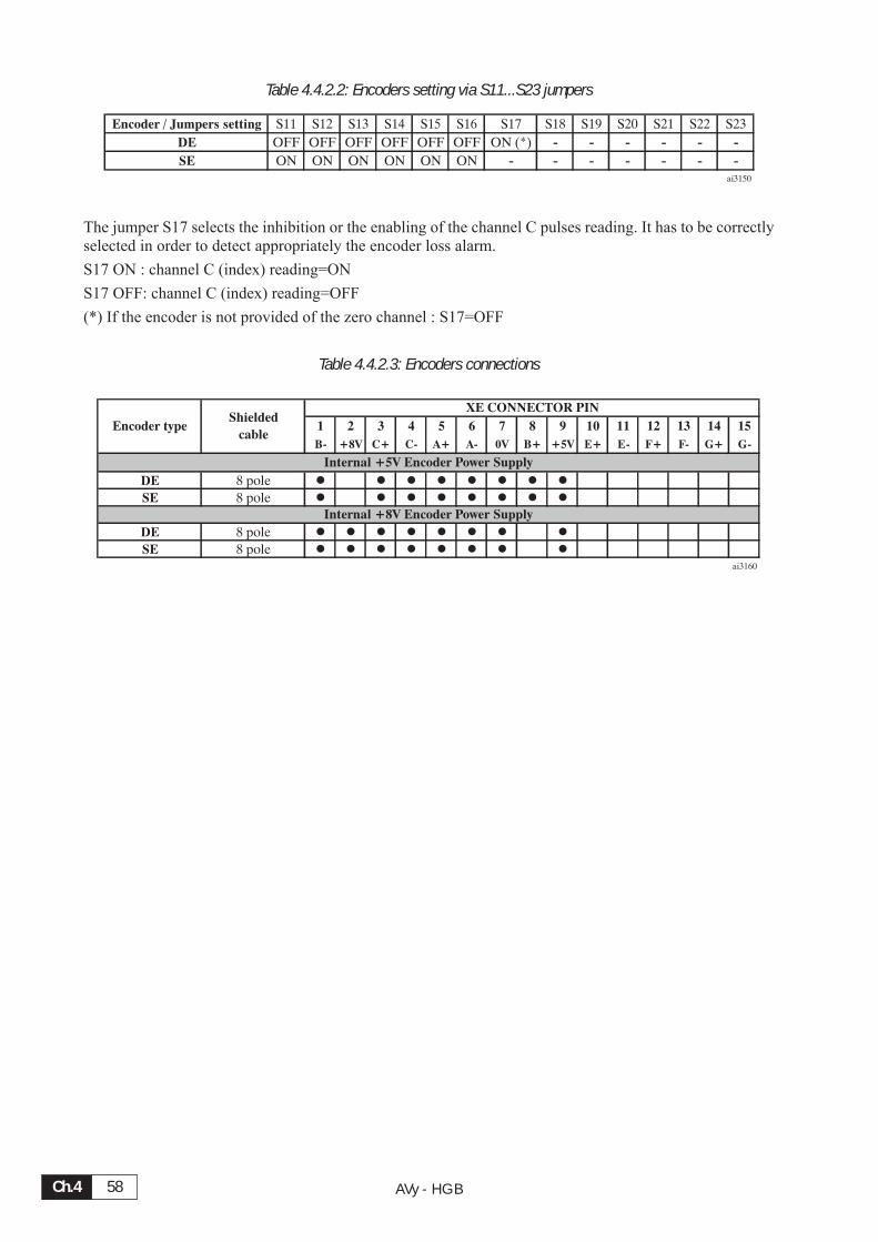
AVy - HGBCh.4 58
Table 4.4.2.2: Encoders setting via S11...S23 jumpers
Encoder / Jumpers setting S11 S12 S13 S14 S15 S16 S17 S18 S19 S20 S21 S22 S23
DE OFF OFF OFF OFF OFF OFF ON (*) - - - - - -
SE ON ON ON ON ON ON - - - - - - -ai3150
The jumper S17 selects the inhibition or the enabling of the channel C pulses reading. It has to be correctlyselected in order to detect appropriately the encoder loss alarm.
S17 ON : channel C (index) reading=ON
S17 OFF: channel C (index) reading=OFF
(*) If the encoder is not provided of the zero channel : S17=OFF
Table 4.4.2.3: Encoders connections
1 2 3 4 5 6 7 8 9 10 11 12 13 14 15
B- +8V C+ C- A+ A- 0V B+ +5V E+ E- F+ F- G+ G-
DE 8 pole � � � � � � � �
SE 8 pole � � � � � � � �
DE 8 pole � � � � � � � �
SE 8 pole � � � � � � � �
ai3160
Internal +8V Encoder Power Supply
XE CONNECTOR PIN
Encoder typeShielded
cable
Internal +5V Encoder Power Supply
Ch.459—————— Installation guidelines ——————
Requirements:
Sinusoidal encoders (XE connector on Regulation card)
max. frequency 80 KHz ( select the appropriate number of pulsesdepending on required max. speed )
Number of pulses per revolution min 600, max 9999
Channels two-channel, differential
Power supply + 5 V (Internal supply) *
Load capacity > 8.3 mA pp per channel
Digital encoders (XE connector on Regulation card)
max. frequency 150 KHz ( select the appropriate number of pulsesdepending on required max. speed )
Number of pulses per revolution min 600, max 9999
Channels - two-channel, differential A / A, B / B, C / C). Anencoder loss detection is possible via firmware setting.
- two channel, (A,B) only with optional card.
Power supply + 5 V (Internal supply) *
Load capacity > 4.5 mA / 6.8 ... 10 mA per channel
* Via keypad (“CONFIGURATION/Motor spd fbk/ Enc 1 supply vlt” menu) it is possible to select 4different values of internal encoder supply voltage to compensate the voltage reduction due to encodercable length and load current encoder.
Selection available are:
- for +5 V encoder supply: 0=5.41V, 1=5.68V, 2=5.91V, 3=6.18V via Enc 1 supply vlt parameter.
- for +8 V encoder supply: leave standard default =0
Encoder power supply test (if the internal supply +5V is used)
During the start up of the drive:
- verify the encoder power supply to the encoders terminals with all the encoders channels connected
- via Enc 1 supply vlt parameter set the appropriate voltage if the encoder supply characteristic (example:+5V ± 5%) is out of range.
Terminals for external encoder connections
Male terminals type: 15 poles high density (VGA type)
Connector cover: Standard 9 poles low profile (Example manufacturer code: AMP0-748676-1, 3M 3357-6509)
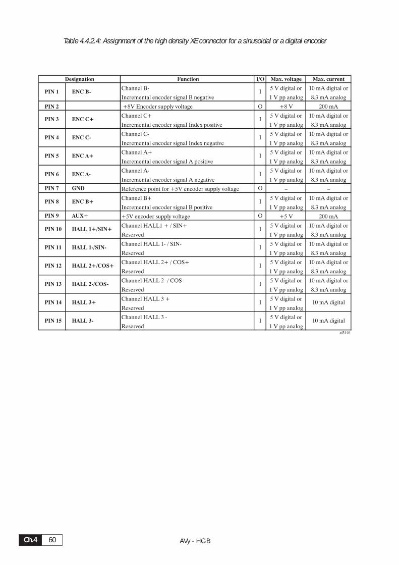
AVy - HGBCh.4 60
Table 4.4.2.4: Assignment of the high density XE connector for a sinusoidal or a digital encoder
Function I/O Max. voltage Max. current
Channel B- 5 V digital or 10 mA digital or
Incremental encoder signal B negative 1 V pp analog 8.3 mA analog
PIN 2 +8V Encoder supply voltage O +8 V 200 mA
Channel C+ 5 V digital or 10 mA digital or
Incremental encoder signal Index positive 1 V pp analog 8.3 mA analog
Channel C- 5 V digital or 10 mA digital or
Incremental encoder signal Index negative 1 V pp analog 8.3 mA analog
Channel A+ 5 V digital or 10 mA digital or
Incremental encoder signal A positive 1 V pp analog 8.3 mA analog
Channel A- 5 V digital or 10 mA digital or
Incremental encoder signal A negative 1 V pp analog 8.3 mA analog
PIN 7 GND Reference point for +5V encoder supply voltage O – –
Channel B+ 5 V digital or 10 mA digital or
Incremental encoder signal B positive 1 V pp analog 8.3 mA analog
PIN 9 AUX+ +5V encoder supply voltage O +5 V 200 mA
Channel HALL1 + / SIN+ 5 V digital or 10 mA digital or
Reserved 1 V pp analog 8.3 mA analog
Channel HALL 1- / SIN- 5 V digital or 10 mA digital or
Reserved 1 V pp analog 8.3 mA analog
Channel HALL 2+ / COS+ 5 V digital or 10 mA digital or
Reserved 1 V pp analog 8.3 mA analog
Channel HALL 2- / COS- 5 V digital or 10 mA digital or
Reserved 1 V pp analog 8.3 mA analog
Channel HALL 3 + 5 V digital or
Reserved 1 V pp analog
Channel HALL 3 - 5 V digital or
Reserved 1 V pp analogai3140
HALL 2+/COS+
HALL 2-/COS-
HALL 3+
HALL 3-
Designation
ENC B-
ENC C-
ENC A+
ENC C+
PIN 1
PIN 3
PIN 4
PIN 5
10 mA digital
10 mA digitalPIN 14
I
I
I
PIN 15 I
PIN 12
PIN 13
I
I
I
I
PIN 10
PIN 11
I
IHALL 1-/SIN-
HALL 1+/SIN+
I
I
PIN 6
PIN 8
ENC A-
ENC B+
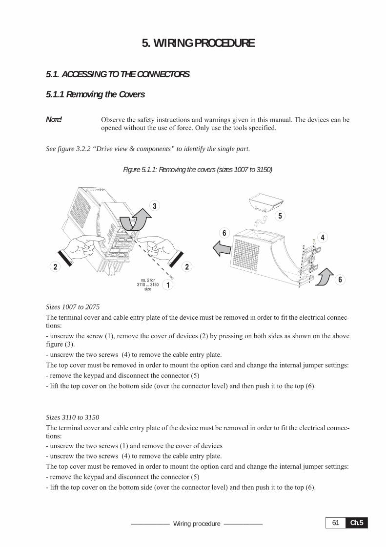
Ch.561—————— Wiring procedure ——————
5. WIRING PROCEDURE
5.1. ACCESSING TO THE CONNECTORS
5.1.1 Removing the Covers
NOTE! Observe the safety instructions and warnings given in this manual. The devices can beopened without the use of force. Only use the tools specified.
See figure 3.2.2 “Drive view & components” to identify the single part.
Figure 5.1.1: Removing the covers (sizes 1007 to 3150)
Sizes 1007 to 2075
The terminal cover and cable entry plate of the device must be removed in order to fit the electrical connec-tions:
- unscrew the screw (1), remove the cover of devices (2) by pressing on both sides as shown on the abovefigure (3).
- unscrew the two screws (4) to remove the cable entry plate.
The top cover must be removed in order to mount the option card and change the internal jumper settings:
- remove the keypad and disconnect the connector (5)
- lift the top cover on the bottom side (over the connector level) and then push it to the top (6).
Sizes 3110 to 3150
The terminal cover and cable entry plate of the device must be removed in order to fit the electrical connec-tions:- unscrew the two screws (1) and remove the cover of devices
- unscrew the two screws (4) to remove the cable entry plate.
The top cover must be removed in order to mount the option card and change the internal jumper settings:
- remove the keypad and disconnect the connector (5)
- lift the top cover on the bottom side (over the connector level) and then push it to the top (6).

AVy - HGBCh.5 62
Figure 5.1.2: Removing the covers (sizes 4220 to 82000)
2 2
1
33
4
Sizes 4220 to 82000
The terminal cover of the device must be removed in order to fit the electrical connections: unscrew the twoscrew (2) and remove the cover (1)
The top cover must be removed in order to mount the option card and change the internal jumper settings:unscrew the two screw (3) and remove the top cover by moving it as indicated on figure (4)
ATTENTION: In order to avoid damages of the device it is not allowed to transport it by handling on itscards !
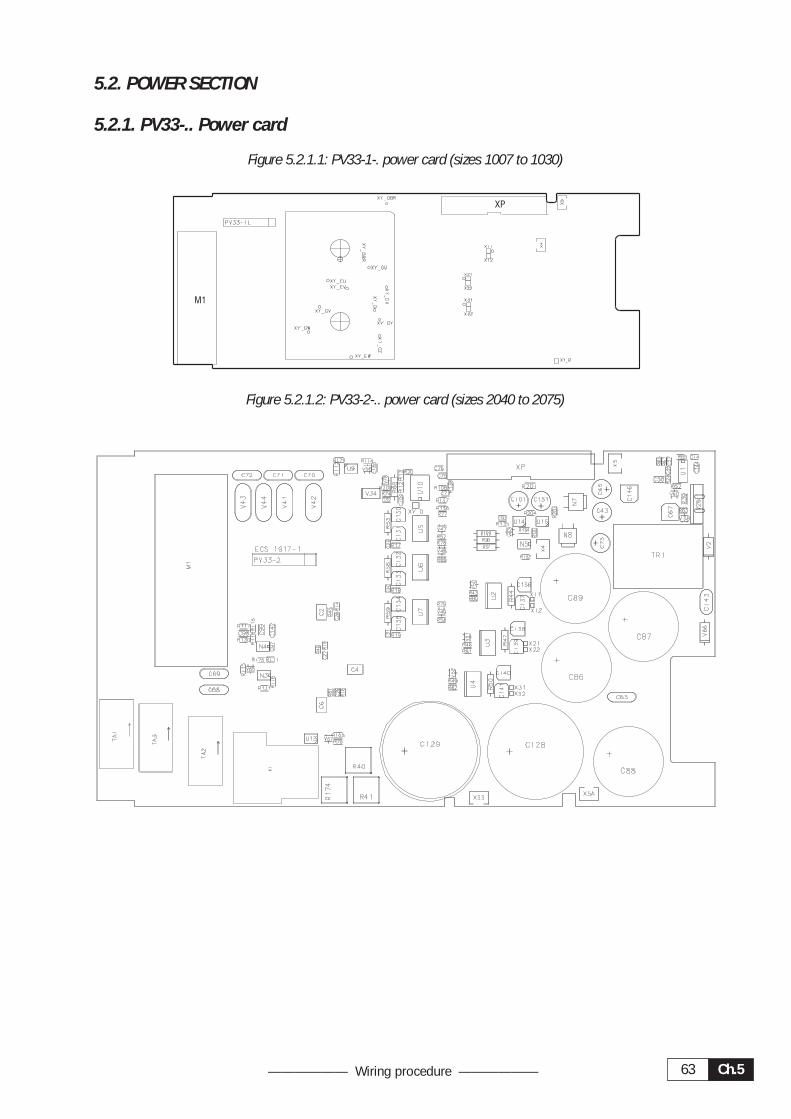
Ch.563—————— Wiring procedure ——————
5.2. POWER SECTION
5.2.1. PV33-.. Power card
Figure 5.2.1.1: PV33-1-. power card (sizes 1007 to 1030)
M1
XP
Figure 5.2.1.2: PV33-2-.. power card (sizes 2040 to 2075)
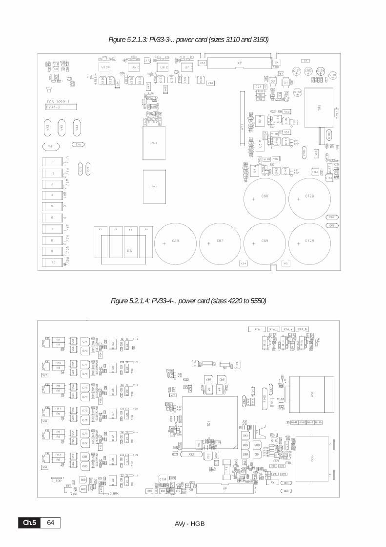
AVy - HGBCh.5 64
Figure 5.2.1.3: PV33-3-.. power card (sizes 3110 and 3150)
Figure 5.2.1.4: PV33-4-.. power card (sizes 4220 to 5550)
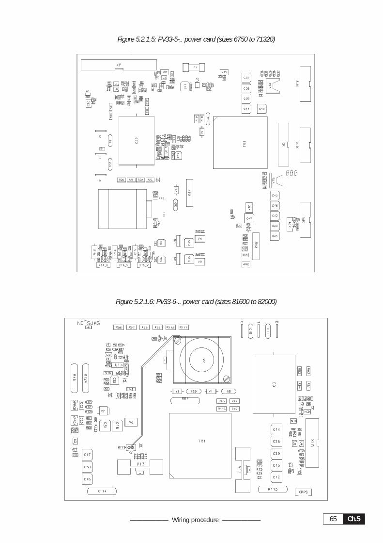
Ch.565—————— Wiring procedure ——————
Figure 5.2.1.5: PV33-5-.. power card (sizes 6750 to 71320)
Figure 5.2.1.6: PV33-6-.. power card (sizes 81600 to 82000)
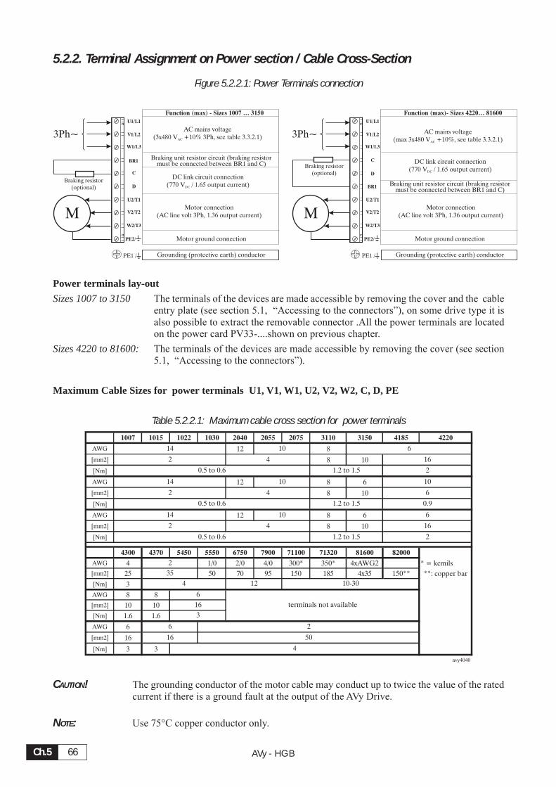
AVy - HGBCh.5 66
5.2.2. Terminal Assignment on Power section / Cable Cross-Section
Figure 5.2.2.1: Power Terminals connection
Function (max) - Sizes 1007 … 3150
Motor ground connection
Braking unit resistor circuit (braking resistormust be connected between BR1 and C)
DC link circuit connection(770 V / 1.65 output current)DC
AC mains voltage(3x480 V +10% 3Ph,AC see table 3.3.2.1)
Motor connection(AC line volt 3Ph, 1.36 output current)
Braking resistor(optional)
M
3Ph~
PE1 / Grounding (protective earth) conductor
U1/L1
V1/L2
W1/L3
BR1
U2/T1
V2/T2
W2/T3
C
D
PE2/ Motor ground connection
Braking unit resistor circuit (braking resistormust be connected between BR1 and C)
AC mains voltage(max 3x480 V +10%, see table 3.3.2.1)AC
Braking resistor(optional)
PE1 / Grounding (protective earth) conductor
U1/L1
V1/L2
W1/L3
BR1
U2/T1
V2/T2
W2/T3
C
D
PE2/
M
3Ph~
Motor connection(AC line volt 3Ph, 1.36 output current)
DC link circuit connection(770 V / 1.65 output current)DC
Function (max)- Sizes 4220… 81600
Power terminals lay-out
Sizes 1007 to 3150 The terminals of the devices are made accessible by removing the cover and the cableentry plate (see section 5.1, “Accessing to the connectors”), on some drive type it isalso possible to extract the removable connector .All the power terminals are locatedon the power card PV33-....shown on previous chapter.
Sizes 4220 to 81600: The terminals of the devices are made accessible by removing the cover (see section5.1, “Accessing to the connectors”).
Maximum Cable Sizes for power terminals U1, V1, W1, U2, V2, W2, C, D, PE
Table 5.2.2.1: Maximum cable cross section for power terminals
1007 1015 1022 1030 2040 2055 2075 3110 3150 4185 4220
AWG 12 8
[mm2] 8 10
[Nm]
AWG 12 8 6
[mm2] 8 10
[Nm]
AWG 12 8 6
[mm2] 8 10
[Nm]
4300 4370 5450 5550 6750 7900 71100 71320 81600 82000
AWG 4 1/0 2/0 4/0 300* 350* 4xAWG2 * = kcmils
[mm2] 25 50 70 95 150 185 4x35 150** **: copper bar
[Nm] 3
AWG 8 8
[mm2] 10 10
[Nm] 1.6 1.6
AWG 6
[mm2] 16
[Nm] 3 3
avy4040
2
2
50
4
6
0.9
6
16
6
16
2
10
2
0.5 to 0.6 1.2 to 1.5
10
4
14
2
10
0.5 to 0.6
1.2 to 1.50.5 to 0.6
4
1.2 to 1.5
14 10
2 4
14
3
6
16
2
35
4 12 10-30
6
terminals not available16
CAUTION! The grounding conductor of the motor cable may conduct up to twice the value of the ratedcurrent if there is a ground fault at the output of the AVy Drive.
NOTE: Use 75°C copper conductor only.
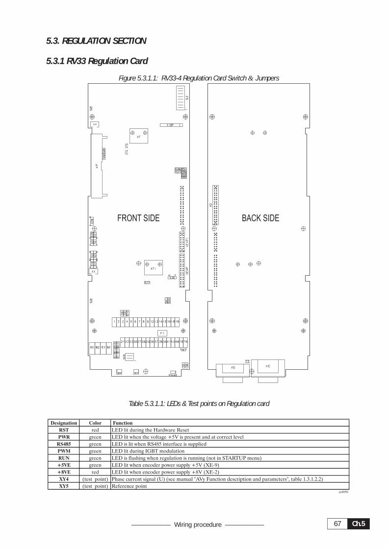
Ch.567—————— Wiring procedure ——————
5.3. REGULATION SECTION
5.3.1 RV33 Regulation Card
Figure 5.3.1.1: RV33-4 Regulation Card Switch & Jumpers
FRONT SIDE BACK SIDE
Table 5.3.1.1: LEDs & Test points on Regulation card
Designation Color Function
RST red LED lit during the Hardware Reset
PWR green LED lit when the voltage +5V is present and at correct level
RS485 green LED is lit when RS485 interface is supplied
PWM green LED lit during IGBT modulation
RUN green LED is flashing when regulation is running (not in STARTUP menu)
+5VE green LED lit when encoder power supply +5V (XE-9)
+8VE red LED lit when encoder power supply +8V (XE-2)
XY4 (test point) Phase current signal (U) (see manual "AVy Function description and parameters", table 1.3.1.2.2)
XY5 (test point) Reference pointai4050

AVy - HGBCh.5 68
Table 5.3.1.3: Jumpers on Regulation Card RV33-3
Designation Function Factory setting
S5 - S6 Terminating resistor for the serial interface RS485 ON (*)
ON= Termination resistor IN
OFF= No termination resistor
S8 Adaptation to the input signal of analog input 1 (terminals 1 and 2) OFFON=0...20 mA / 4...20 mA
OFF=0...10 V / -10...+10 V
S9 Adaptation to the input signal of analog input 2 (terminals 3 and 4) OFFON=0...20 mA / 4...20 mA
OFF=0...10 V / -10...+10 V
S10 Adaptation to the input signal of analog input 3 (terminals 5 and 6) OFFON=0...20 mA / 4...20 mA
OFF=0...10 V / -10...+10 V
S11 - S12 - S13 Encoder setting ( jumpers on kit EAM_1618 supplied with the drive) OFF
S14 - S15 - S16 ON=Sinusoidal SE
OFF=Digital DE
S17 Monitoring of the C-channel of the digital encoder OFFON=C-Channel monitored
OFF=C-Channel not monitored (required for single-ended channels)
S18 - S19 Encoder setting B
S20 - S21 Pos. B= reserved
Pos. A= reserved
S22 - S23 Analog input 3 enabling (alternative with SESC encoder) B
Pos. A= reserved
Pos. B=analog input 3 enabled
Pos. OFF= resolver
S26 - S27 Reserved ON
S28 Encoder Internal power supply selection
ON / ON = +5 V
OFF / OFF = +8 V
ON/ON
S29 Internal use A
S30 Second encoder qualifier input
A=from EXP-… board
B=from digital input "3" on RV33-4
A
Jumper to disconnect 0V (+24V power supply) from ground ON
ON = 0V connected to ground (hard-wire)
OFF = 0V disconnected from ground
Jumper to disconnect 0V (regulation board) from ground ON
ON = 0V connected to ground (hard-wire)
OFF = 0V disconnected from ground
S36 Internal use not mounted
S37 Internal use not mounted
S38-S39 Internal use ON
Power supply for the serial interface RS485 OFF
ON = Internal power supply (from pins XS.5 / XS.9)
OFF = External power supply (to pins XS.5 / XS.9)
Ay4060
(*) on multidrop connection the jumper must be ON only for the last drop of a serial line(**) see chapter 5.4
S40-S41
(**)
S34
S35
Table 5.3.1.4: RV33 Regulation Card Switch S3 SettingsType 1007 1015 1022 1030 2040 2055 2075 3110 3150 4185 4220 4300 4370 5450 5550 6750 7900 71100 71320 81600 82000
S3-1 ON OFF ON OFF OFF ON OFF ON OFF OFF ON OFF ON OFF ON OFF ON OFF ON OFF ON
S3-2 OFF ON ON OFF OFF OFF ON ON OFF ON OFF ON ON OFF OFF ON ON OFF OFF ON OFF
S3-3 OFF OFF OFF OFF ON OFF OFF OFF ON ON ON ON ON OFF OFF OFF OFF ON ON ON ON
S3-4 OFF OFF OFF OFF OFF OFF OFF OFF OFF ON OFF OFF OFF ON ON ON ON ON ON ON ON
S3-5 ON ON ON OFF ON OFF OFF OFF OFF ON OFF OFF OFF OFF OFF OFF OFF OFF OFF OFF ON
S3-6 OFF OFF OFF OFF OFF OFF OFF OFF OFF OFF OFF OFF OFF OFF OFF OFF OFF OFF OFF OFF OFF
S3-7 ON ON ON ON ON ON ON ON ON ON ON ON ON ON ON ON ON ON ON ON ON
S3-8 OFF OFF OFF OFF OFF OFF OFF OFF OFF OFF OFF OFF OFF OFF OFF OFF OFF OFF OFF OFF OFF
avy4080
The devices are factory set accordingly.When fitting a regulation card as a spare, remember to set dip-switch S3 and encoder
jumpers accordingly.
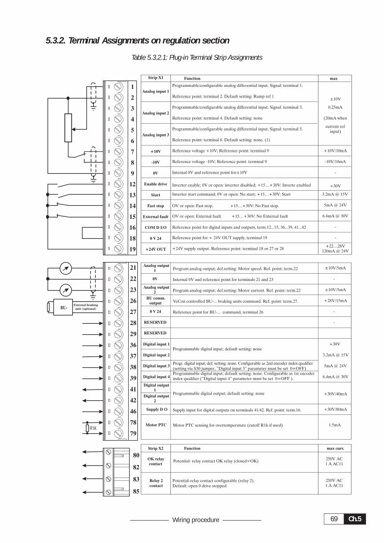
Ch.569—————— Wiring procedure ——————
5.3.2. Terminal Assignments on regulation section
Table 5.3.2.1: Plug-in Terminal Strip Assignments
1
2
3
4
5
6
7
8
9
12
13
14
15
16
18
19
BU-External braking
unit (optional)
Strip X1 Function max
Programmable/configurable analog differential input. Signal: terminal 1.
Reference point: terminal 2. Default setting: Ramp ref 1±10V
Programmable/configurable analog differential input. Signal: terminal 3. 0.25mA
Reference point: terminal 4. Default setting: none (20mA when
Programmable/configurable analog differential input. Signal: terminal 5.current ref
input)
Reference point: terminal 6. Default setting: none. (1)
+10V Reference voltage +10V; Reference point: terminal 9 +10V/10mA
-10V Reference voltage -10V; Reference point: terminal 9 -10V/10mA
0V Internal 0V and reference point for±10V -
Enable drive Inverter enable; 0V or open: inverter disabled; +15…+30V: Inverte enabled +30V
Start Inverter start command; 0V or open: No start; +15…+30V: Start 3.2mA @ 15V
Fast stop OV or open: Fast stop. +15…+30V: No Fast stop. 5mA @ 24V
External fault OV or open: External fault. +15…+30V: No External fault 6.4mA @ 30V
COM D I/O Reference point for digital inputs and outputs, term.12...15, 36...39, 41...42 -
0 V 24 Reference point for + 24V OUT supply, terminal 19 -
+24V OUT +24V supply output. Reference point: terminal 18 or 27 or 28+22…28V
120mA @ 24V
Analog input 1
Analog input 2
Analog input 3
Analog output
1 Program.analog output; def.setting: Motor speed. Ref. point: term.22 ±10V/5mA
0V Internal 0V and reference point for terminals 21 and 23 -
Analog output
2 Program.analog output; def.setting: Motor current. Ref. point: term.22 ±10V/5mA
BU comm.
output VeCon controlled BU-... braking units command. Ref. point: term.27. +28V/15mA
0 V 24 Reference point for BU-... command, terminal 26 -
RESERVED -
Digital input 1 +30V
Digital input 2 3.2mA @ 15V
Digital input 3 5mA @ 24V
Digital input 4 6.4mA @ 30V
Digital output
1+30V/40mA
Digital output
2
Supply D O Supply input for digital outputs on terminals 41/42. Ref. point: term.16. +30V/80mA
Motor PTC 1.5mA
Programmable digital output; default setting: none
Motor PTC sensing for overtemperature (cutoff R1k if used)
Programmable digital input; default setting: none
21
22
23
26
27
28
29
36
37
38
39
41
42
46
78
79R1K
Strip X2 Function max curr.
250V AC1 A AC11
250V AC1 A AC11
OK relay
contact
Potential-relay contact configurable (relay 2).Default: open 0 drive stopped
Relay 2
contact
Potential- relay contact OK relay (closed=OK)80
82
83
85
RESERVED
Programmable digital input; default setting: none. Configurable as 1st encoderindex qualifier (”Digital input 4” parameter must be set 0=OFF ).
Progr. digital input; def. setting: none. Configurable as 2nd encoder index qualifier(setting via S30 jumper, )”Digital input 3” parameter must be set 0=OFF
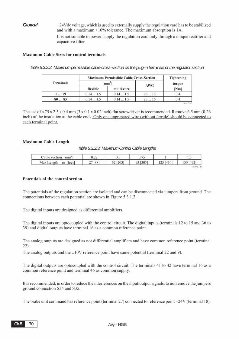
AVy - HGBCh.5 70
CAUTION! +24Vdc voltage, which is used to externally supply the regulation card has to be stabilizedand with a maximum ±10% tolerance. The maximum absorption is 1A.
It is not suitable to power supply the regulation card only through a unique rectifier andcapacitive filter.
Maximum Cable Sizes for control terminals
Table 5.3.2.2: Maximum permissible cable cross-section on the plug-in terminals of the regulator section
Maximum Permissible Cable Cross-Section Tightening
[mm2] torque
flexible multi-core [Nm]
1 ... 79 0.14 ... 1.5 0.14 ... 1.5 28 ... 16 0.4
80 ... 85 0.14 ... 1.5 0.14 ... 1.5 28 ... 16 0.4Ai4090
AWGTerminals
The use of a 75 x 2.5 x 0.4 mm (3 x 0.1 x 0.02 inch) flat screwdriver is recommended. Remove 6.5 mm (0.26inch) of the insulation at the cable ends. Only one unprepared wire (without ferrule) should be connected toeach terminal point.
Maximum Cable Length
Table 5.3.2.3: Maximum Control Cable Lengths
Cable section [mm2] 0.22 0.5 0.75 1 1.5
Max Length m [feet] 27 [88] 62 [203] 93 [305] 125 [410] 150 [492]avy3130
Potentials of the control section
The potentials of the regulation section are isolated and can be disconnected via jumpers from ground. Theconnections between each potential are shown in Figure 5.3.1.2.
The digital inputs are designed as differential amplifiers.
The digital inputs are optocoupled with the control circuit. The digital inputs (terminals 12 to 15 and 36 to39) and digital outputs have terminal 16 as a common reference point.
The analog outputs are designed as not differential amplifiers and have common reference point (terminal22).
The analog outputs and the ±10V reference point have same potential (terminal 22 and 9).
The digital outputs are optocoupled with the control circuit. The terminals 41 to 42 have terminal 16 as acommon reference point and terminal 46 as common supply.
It is recommended, in order to reduce the interferences on the input/output signals, to not remove the jumpersground connection S34 and S35.
The brake unit command has reference point (terminal 27) connected to reference point +24V (terminal 18).
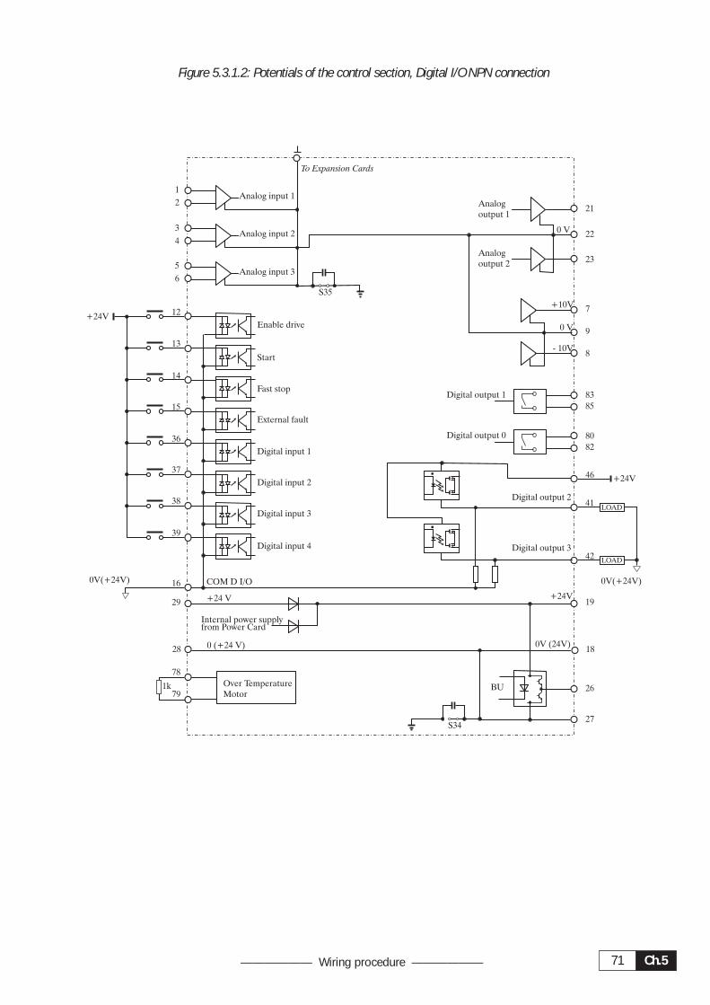
Ch.571—————— Wiring procedure ——————
Figure 5.3.1.2: Potentials of the control section, Digital I/O NPN connection
1
2
3
4
5
6
+24V
13
14
15
36
37
38
39
16
29
28
Over TemperatureMotor
1k
Analog input 1
Analog input 2
Analog input 3
Enable drive
Start
Fast stop
External fault
Digital input 1
Digital input 2
Digital input 3
Digital input 4
Internal power supplyfrom Power Card
COM D I/O
+24 V
0 (+24 V)
78
79
Analogoutput 2
21
220 V
23
7
9
8
+10V
- 10V
0 V
8385
8082
Digital output 1
Digital output 0
46
41
42
Digital output 2
Digital output 3
19
18
26
27
+24V
0V (24V)
BU
To Expansion Cards
S35
S34
Analogoutput 1
0V(+24V)
LOAD
+24V
0V(+24V)
LOAD
12
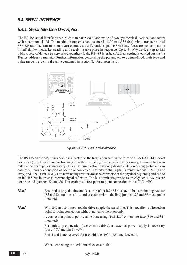
AVy - HGBCh.5 72
5.4. SERIAL INTERFACE
5.4.1. Serial Interface Description
The RS 485 serial interface enables data transfer via a loop made of two symmetrical, twisted conductorswith a common shield. The maximum transmission distance is 1200 m (3936 feet) with a transfer rate of38.4 KBaud. The transmission is carried out via a differential signal. RS 485 interfaces are bus-compatiblein half-duplex mode, i.e. sending and receiving take place in sequence. Up to 31 AVy devices (up to 128address selectable) can be networked together via the RS 485 interface. Address setting is carried out via theDevice address parameter. Further information concerning the parameters to be transfered, their type andvalue range is given in the table contained in section 8, “Parameter lists”.
12345
9 8 7 6
150 R
TxA/RxA
TxB/RxB
0 V S
+5 V S
S5 S6
PE
RS485
XS
100
R
470
R
470
R
+5 V
S41
S40
Figure 5.4.1.1: RS485 Serial Interface
The RS 485 on the AVy series devices is located on the Regulation card in the form of a 9-pole SUB-D socketconnector (XS).The communication may be with or without galvanic isolation: by using galvanic isolation anexternal power supply is necessary (+5V). Communication without galvanic isolation are suggested only incase of temporary connection of one drive connected. The differential signal is transferred via PIN 3 (TxA/RxA) and PIN 7 (TxB/RxB). Bus terminating resistors must be connected at the physical beginning and end ofan RS 485 bus in order to prevent signal reflexion. The bus terminating resistors on AVy series devices areconnected via jumpers S5 and S6. This enables a direct point-to-point connection with a PLC or PC.
NOTE! Ensure that only the first and last drop of an RS 485 bus have a bus terminating resistor(S5 and S6 mounted). In all other cases (within the line) jumpers S5 and S6 must not bemounted.
NOTE! With S40 and S41 mounted the drive supply the serial line. This modality is allowed onpoint-to-point connection without galvanic isolation only.
A connection point to point can be done using “PCI-485” option interface (S40 and S41mounted).
For multidrop connection (two or more drive), an external power supply is necessary(pin 5 / 0V and pin 9 / +5V).
Pins 6 and 8 are reserved for use with the “PCI-485” interface card.
When connecting the serial interface ensure that
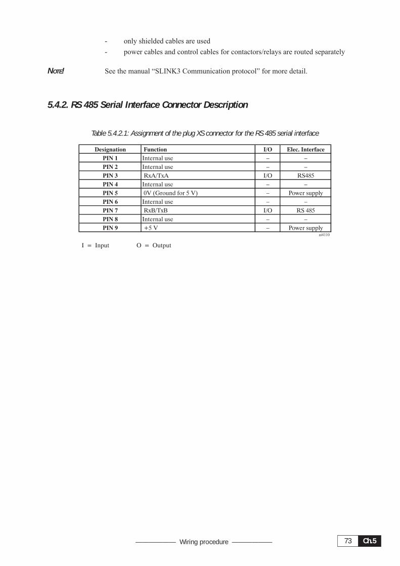
Ch.573—————— Wiring procedure ——————
- only shielded cables are used
- power cables and control cables for contactors/relays are routed separately
NOTE! See the manual “SLINK3 Communication protocol” for more detail.
5.4.2. RS 485 Serial Interface Connector Description
Table 5.4.2.1: Assignment of the plug XS connector for the RS 485 serial interface
Designation Function I/O Elec. Interface
PIN 1 Internal use – –
PIN 2 Internal use – –
PIN 3 RxA/TxA I/O RS485
PIN 4 Internal use – –
PIN 5 0V (Ground for 5 V) – Power supply
PIN 6 Internal use – –
PIN 7 RxB/TxB I/O RS 485
PIN 8 Internal use – –
PIN 9 +5 V – Power supplyai4110
I = Input O = Output
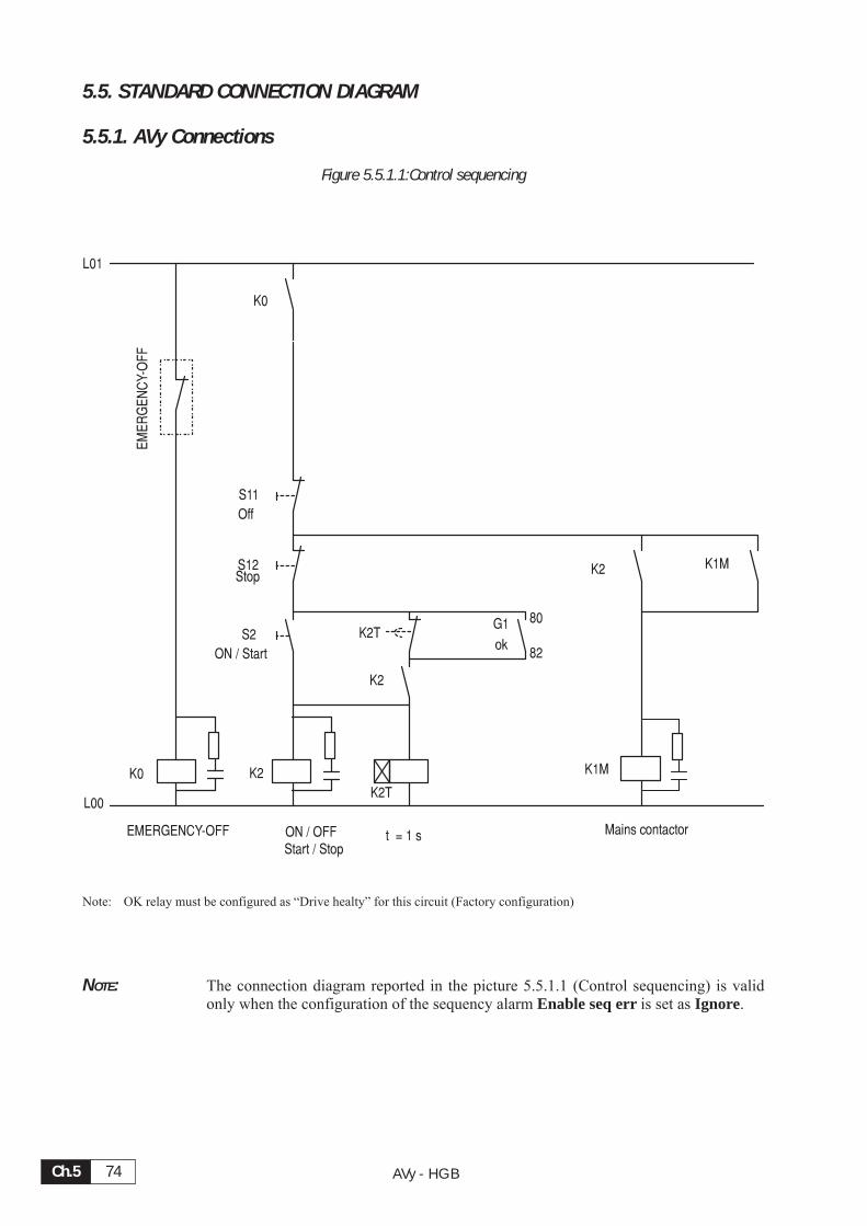
AVy - HGBCh.5 74
5.5. STANDARD CONNECTION DIAGRAM
5.5.1. AVy Connections
Figure 5.5.1.1:Control sequencing
EM
ER
GE
NC
Y-O
FF
EMERGENCY-OFF
K0
K0
S11
Off
S12Stop
S2
ON / Start
ON / OFFStart / Stop
K2
K2T
K2T
K2
G1 80
82ok
t = 1 s
K2 K1M
K1M
Mains contactor
L01
L00
Note: OK relay must be configured as “Drive healty” for this circuit (Factory configuration)
NOTE: The connection diagram reported in the picture 5.5.1.1 (Control sequencing) is validonly when the configuration of the sequency alarm Enable seq err is set as Ignore.
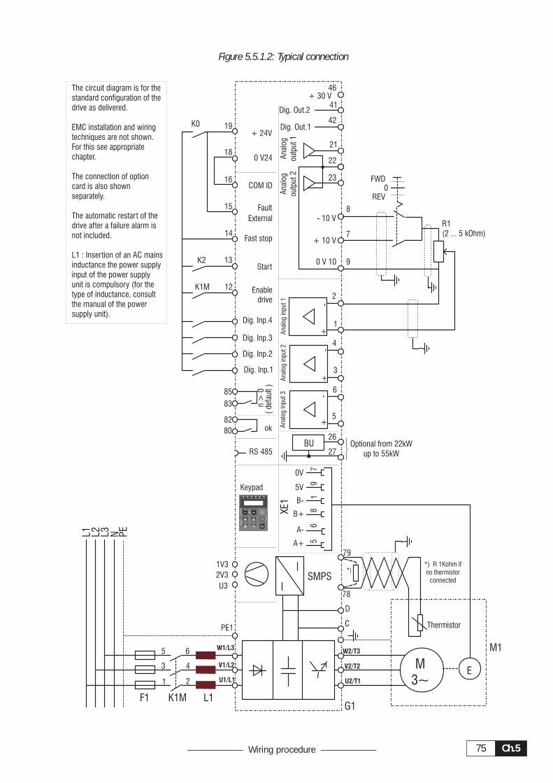
Ch.575—————— Wiring procedure ——————
Figure 5.5.1.2: Typical connection
+ 24V
U1/L1
M1
K1M
5
F1
L1 L2 L3 N PE
K2
G1
0 V24
C
D
1 2
3 4
6
K1M
SMPS
K0
L1
Thermistor
78
79
B-
1
A+ 5
A-
6
B+
87
0V
9
5V
XE1
COM ID
19
18
16
15
External
Fault
14
13
12
Fast stop
Start
Enabledrive
80
82
83
85
ok
n>
0(
defa
ult)
RS 485
Keypad
7
8
9
+ 10 V
- 10 V
0 V 10
0FWD
REV
R1(2 ... 5 kOhm)
2
1
Ana
log
inpu
t1
Ana
log
inpu
t2
-
3
4-+
+
Ana
log
inpu
t3
5
6-+
E
*) R 1Kohm ifno thermistor
connected
*)
PE1
V1/L2
W1/L3
U2/T1
V2/T2
W2/T3
Dig. Inp.1
Dig. Inp.2
Dig. Inp.3
Dig. Inp.4
Ana
log
outp
ut2
Ana
log
outp
ut1
21
22
23
42
46
41+ 30 V
Dig. Out.1
Dig. Out.2
27
26BU
1V3
U3
2V3
Optional from 22kWup to 55kW
M3~
The circuit diagram is for thestandard configuration of thedrive as delivered.
EMC installation and wiringtechniques are not shown.For this see appropriatechapter.
The connection of optioncard is also shownseparately.
The automatic restart of thedrive after a failure alarm isnot included.
L1 : Insertion of an AC mainsinductance the power supplyinput of the power supplyunit is compulsory (for thetype of inductance, consultthe manual of the powersupply unit).

AVy - HGBCh.5 76
5.5.2. Parallel Connection on the AC (Input) and DC (Intermediate Circuit) Side ofSeveral Inverters
Features and Limits:
1 The inverters used have to be all the same size.
2 AC line chokes (see chapter 5.7.1) have to be the same (provided by the same supplier).
3 The mains power supply has to be simultaneous for all inverters, i.e. a single switch /line contactor has tobe used.
4 Such connection is suitable for a maximum of 6 inverters.
5 If necessary dissipate braking energy; a single internal braking unit (with external resistor) has to be usedor one (or several) external braking unit ("BU32-.., BUy-...”) configured with the inverter or a BU asmaster (all the other connected BUs are configured as slaves).
6 Fast fuses (F12...F62) have to be fitted on the dc-link side ( C and D terminals) of each inverters (seechapter 5.6.2).
(*) ATTENTION ! Do not connect if external braking unit are used.
Figure 5.5.2.1: Parallel Connection on the AC and DC Side of Several Inverters
M13
M23
M63
F11 L1
F21 L2
F61 L6
U
V
W
U2
V2
W2
C
D
INVERTER 1
U
V
W
U2
V2
W2
C
D
INVERTER 2
BR
F12
F22
F62
U
V
W
U2
V2
W2
C
D
INVERTER 6
2627(0V24)
BR
CR C
D
BU-32-...(B y-...)U
(SLAVE)
7 8 9 10
RBR
F7
RBR
L1
L2
L3
K1
M..3
F.. L..
U
V
W
U2
V2
W2
C
D
INVERTER ..
F..
(*)
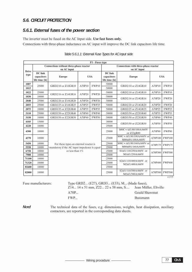
Ch.577—————— Wiring procedure ——————
5.6. CIRCUIT PROTECTION
5.6.1. External fuses of the power section
The inverter must be fused on the AC Input side. Use fast fuses only.
Connections with three-phase inductance on AC input will improve the DC link capacitors life time.
Table 5.6.1.1: External Fuse Types for AC input side
DC link
capacitors
life time [h]
Europe USA
DC link
capacitors
life time [h]
Europe USA
1007 50000
1015 50000
1022 25000 50000 GRD2/10 or Z14GR10 A70P10 FWP10
1030 10000 50000
2040 25000 GRD2/20 or Z14GR20 A70P20 FWP20 50000
2055 25000 GRD2/25 or Z14GR25 A70P25 FWP25 50000 GRD2/20 or Z14GR20 A70P20 FWP20
2075 10000 GRD3/35 or Z22GR40 A70P35 FWP35 50000 GRD2/25 or Z14GR25 A70P25 FWP25
3110 25000 GRD3/50 or Z22GR40 A70P40 FWP40 50000 GRD3/50 or Z22GR40 A70P35 FWP35
3150 10000 GRD3/50 or Z22GR50 A70P40 FWP50 50000 GRD3/50 or Z22GR50 A70P40 FWP40
4185 15000 30000
4220 10000 25000
4300 10000 25000S00C+/üf1/80/100A/660V
or Z22gR80A70P80 FWP80
4370 10000 25000S00C+/üf1/80/100A/660V or
M00üf01/100A/660VA70P100 FWP100
5450 10000 25000
5550 10000 25000
6750 10000 25000
7900 10000 25000
71100 10000 25000
71320 10000 25000
81600 10000 25000
82000 10000 25000S2üf1/110/500A/660V or
M2üf1/500A/660VA70P500 FWP500
avy4120
F1 - Fuses type
Drive
type
Connections with three-phase reactor
on AC input
GRD2/10 or Z14GR10 A70P10 FWP10GRD2/10 or Z14GR10
Connections without three-phase reactor
on AC input
25000 A70P10 FWP10
GRD2/16 or Z14GR16
S00C+/üf1/80/160A/660V or
M00üf01/160A/660VA70P175 FWP175
GRD2/16 or Z14GR16 FWP20A70P20
A70P20 FWP20
For these types an external reactor is
mandatory if the AC input impedence is equal
or less than 1%
GRD3/50 or Z22GR50 A70P50 FWP50
A70P300 FWP300
S2üf1/110/400A/660V or
M2üf1/400A/660VA70P400 FWP400
S1üf1/110/250A/660V or
M1üf1/250A/660V
Fuse manufacturers: Type GRD2... (E27), GRD3... (E33), M... (blade fuses),Z14... 14 x 51 mm, Z22... 22 x 58 mm, S.... Jean Müller, Eltville
A70P... Gould Shawmut
FWP... Bussmann
NOTE! The technical data of the fuses, e.g. dimensions, weights, heat dissipation, auxiliarycontactors, are reported in the corresponding data sheets.
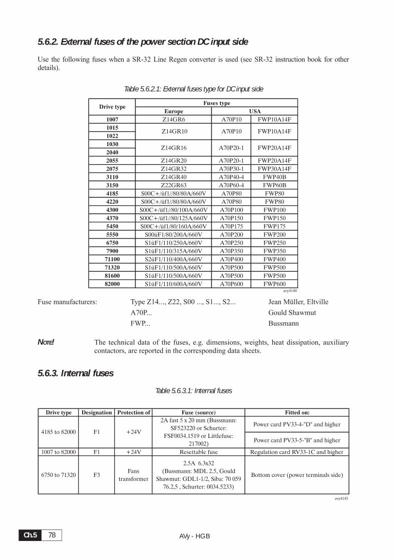
AVy - HGBCh.5 78
5.6.2. External fuses of the power section DC input side
Use the following fuses when a SR-32 Line Regen converter is used (see SR-32 instruction book for otherdetails).
Table 5.6.2.1: External fuses type for DC input side
Fuses type
Europe USA
1007 Z14GR6 A70P10 FWP10A14F
1015
1022
1030
2040
2055 Z14GR20 A70P20-1 FWP20A14F
2075 Z14GR32 A70P30-1 FWP30A14F
3110 Z14GR40 A70P40-4 FWP40B
3150 Z22GR63 A70P60-4 FWP60B
4185 S00C+/üf1//80/80A/660V A70P80 FWP80
4220 S00C+/üf1//80/80A/660V A70P80 FWP80
4300 S00C+/üf1//80/100A/660V A70P100 FWP100
4370 S00C+/üf1//80/125A/660V A70P150 FWP150
5450 S00C+/üf1/80/160A/660V A70P175 FWP175
5550 S00üF1/80/200A/660V A70P200 FWP200
6750 S1üF1/110/250A/660V A70P250 FWP250
7900 S1üF1/110/315A/660V A70P350 FWP350
71100 S2üF1/110/400A/660V A70P400 FWP400
71320 S1üF1/110/500A/660V A70P500 FWP500
81600 S1üF1/110/500A/660V A70P500 FWP500
82000 S1üF1/110/600A/660V A70P600 FWP600avy4140
Z14GR16 A70P20-1 FWP20A14F
Drive type
Z14GR10 A70P10 FWP10A14F
Fuse manufacturers: Type Z14..., Z22, S00 ..., S1..., S2... Jean Müller, Eltville
A70P... Gould Shawmut
FWP... Bussmann
NOTE! The technical data of the fuses, e.g. dimensions, weights, heat dissipation, auxiliarycontactors, are reported in the corresponding data sheets.
5.6.3. Internal fuses
Table 5.6.3.1: Internal fuses
Drive type Designation Protection of Fuse (source) Fitted on:
Power card PV33-4-"D" and higher
Power card PV33-5-"B" and higher
1007 to 82000 F1 +24V Resettable fuse Regulation card RV33-1C and higher
6750 to 71320 F3Fans
transformer
2.5A 6.3x32
(Bussmann: MDL 2.5, Gould
Shawmut: GDL1-1/2, Siba: 70 059
76.2,5 , Schurter: 0034.5233)
Bottom cover (power terminals side)
avy4145
2A fast 5 x 20 mm (Bussmann:
SF523220 or Schurter:
FSF0034.1519 or Littlefuse:
217002)
4185 to 82000 F1 +24V
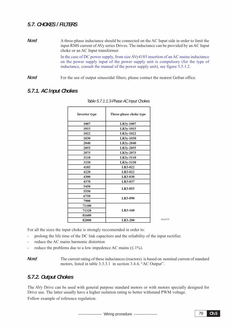
Ch.579—————— Wiring procedure ——————
5.7. CHOKES / FILTERS
NOTE! A three-phase inductance should be connected on the AC Input side in order to limit theinput RMS current of AVy series Drives. The inductance can be provided by an AC Inputchoke or an AC Input transformer.
In the case of DC power supply, from size AVy4185 insertion of an AC mains inductanceon the power supply input of the power supply unit is compulsory (for the type ofinductance, consult the manual of the power supply unit), see figure 5.5.1.2.
NOTE! For the use of output sinusoidal filters, please contact the nearest Gefran office.
5.7.1. AC Input Chokes
Table 5.7.1.1:3-Phase AC Input Chokes
Inverter type Three-phase choke type
1007 LR3y-1007
1015 LR3y-1015
1022 LR3y-1022
1030 LR3y-1030
2040 LR3y-2040
2055 LR3y-2055
2075 LR3y-2075
3110 LR3y-3110
3150 LR3y-3150
4185 LR3-022
4220 LR3-022
4300 LR3-030
4370 LR3-037
5450
5550
6750
7900
71100
71320
81600
82000 LR3-200 Avy4135
LR3-055
LR3-090
LR3-160
For all the sizes the input choke is strongly reccomended in order to:
- prolong the life time of the DC link capacitors and the reliability of the input rectifier.- reduce the AC mains harmonic distortion
- reduce the problems due to a low impedence AC mains (≤ 1%).
NOTE! The current rating of these inductances (reactors) is based on nominal current of standardmotors, listed in table 3.3.3.1 in section 3.4.4, “AC Output”.
5.7.2. Output Chokes
The AVy Drive can be used with general purpose standard motors or with motors specially designed forDrive use. The latter usually have a higher isolation rating to better withstand PWM voltage.
Follow example of reference regulation:
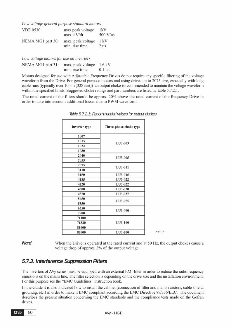
AVy - HGBCh.5 80
Low voltage general purpose standard motors
VDE 0530: max peak voltage 1kVmax. dV/dt 500 V/us
NEMA MG1 part 30: max. peak voltage 1 kVmin. rise time 2 us
Low voltage motors for use on inverters
NEMA MG1 part 31: max. peak voltage 1.6 kVmin. rise time 0.1 us.
Motors designed for use with Adjustable Frequency Drives do not require any specific filtering of the voltagewaveform from the Drive. For general purpose motors and using drives up to 2075 size, especially with longcable runs (typically over 100 m [328 feet]) an output choke is recommended to mantain the voltage waveformwithin the specified limits. Suggested choke ratings and part numbers are listed in table 5.7.2.1.
The rated current of the filters should be approx. 20% above the rated current of the frequency Drive inorder to take into account additional losses due to PWM waveform.
Table 5.7.2.1: Recommended values for output chokes
Inverter type Three-phase choke type
1007
1015
1022
1030
2040
2055
2075
3110
3150 LU3-015
4185 LU3-022
4220 LU3-022
4300 LU3-030
4370 LU3-037
5450
5550
6750
7900
71100
71320
81600
82000 LU3-200 Avy4150
LU3-160
LU3-055
LU3-090
LU3-003
LU3-005
LU3-011
NOTE! When the Drive is operated at the rated current and at 50 Hz, the output chokes cause avoltage drop of approx. 2% of the output voltage.
5.7.3. Interference Suppression Filters
The inverters of AVy series must be equipped with an external EMI filter in order to reduce the radiofrequencyemissions on the mains line. The filter selection is depending on the drive size and the installation environment.For this purpose see the “EMC Guidelines” instruction book.
In the Guide it is also indicated how to install the cabinet (connection of filter and mains reactors, cable shield,groundig, etc.) in order to make it EMC compliant according the EMC Directive 89/336/EEC. The documentdescribes the present situation concerning the EMC standards and the compliance tests made on the Gefrandrives.
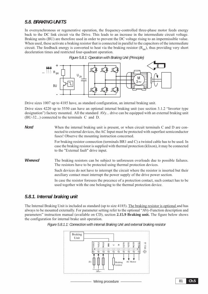
Ch.581—————— Wiring procedure ——————
5.8. BRAKING UNITS
In oversynchronous or regenerative operation, the frequency-controlled three-phase motor feeds energyback to the DC link circuit via the Drive. This leads to an increase in the intermediate circuit voltage.Braking units (BU) are therefore used in order to prevent the DC voltage rising to an impermissible value.When used, these activate a braking resistor that is connected in parallel to the capacitors of the intermediatecircuit. The feedback energy is converted to heat via the braking resistor (R
BR), thus providing very short
deceleration times and restricted four-quadrant operation.
Figure 5.8.1: Operation with Braking Unit (Principle)
E
3M
_R
BR
BU
UZK
Drive sizes 1007 up to 4185 have, as standard configuration, an internal braking unit.
Drive sizes 4220 up to 5550 can have an optional internal braking unit (see section 3.1.2 “Inverter typedesignation”) factory mounted. All the standard AVy... drive can be equipped with an external braking unit(BU-32...) connected to the terminals C and D.
NOTE! When the internal braking unit is present, or when circuit terminals C and D are con-nected to external devices, the AC Input must be protected with superfast semiconductorfuses! Observe the mounting instruction concerned.
For braking resistor connection (terminals BR1 and C) a twisted cable has to be used. Incase the braking resistor is supplied with thermal protection (klixon), it may be connectedto the "External fault" drive input.
WARNING! The braking resistors can be subject to unforeseen overloads due to possible failures.The resistors have to be protected using thermal protection devices.
Such devices do not have to interrupt the circuit where the resistor is inserted but theirauxiliary contact must interrupt the power supply of the drive power section.
In case the resistor foresees the precence of a protection contact, such contact has to beused together with the one belonging to the thermal protection device.
5.8.1. Internal braking unit
The Internal Braking Unit is included as standard (up to size 4185). The braking resistor is optional and hasalways to be mounted externally. For parameter setting refer to the optional “AVy-Function description andparameters” instruction manual (available on CD), section 2.15.9 Braking unit. The figure below showsthe configuration for internal brake unit operation.
Figure 5.8.1.1: Connection with internal Braking Unit and external braking resistor
Brakingresistor
3Ph~
PE
1/
U1
/L1
V1
/L2
W1
/L3
BR
1
U2
/T1
V2
/T2
W2
/T3
C D
PE
2/
F1
BrakingUnit
AC Motor
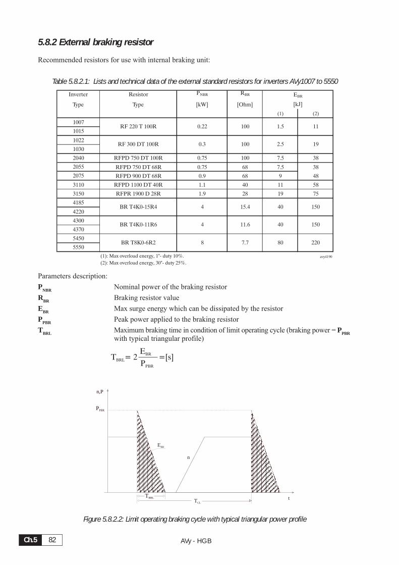
AVy - HGBCh.5 82
5.8.2 External braking resistor
Recommended resistors for use with internal braking unit:
Table 5.8.2.1: Lists and technical data of the external standard resistors for inverters AVy1007 to 5550
Inverter Resistor PNBR RBR
Type Type [kW] [Ohm]
(1) (2)
1007
1015
1022
1030
2040 RFPD 750 DT 100R 0.75 100 7.5 38
2055 RFPD 750 DT 68R 0.75 68 7.5 38
2075 RFPD 900 DT 68R 0.9 68 9 48
3110 RFPD 1100 DT 40R 1.1 40 11 58
3150 RFPR 1900 D 28R 1.9 28 19 75
4185
4220
4300
4370
5450
5550
(1): Max overload energy, 1"- duty 10%. avy4190
(2): Max overload energy, 30"- duty 25%.
40 150BR T4K0-11R6
BR T8K0-6R2
4
8
11.6
7.7 80 220
BR T4K0-15R4 4 15.4
RF 220 T 100R 0.22 100
RF 300 DT 100R 0.3 100
EBR
[kJ]
40 150
19
1.5 11
2.5
Parameters description:
PNBR
Nominal power of the braking resistor
RBR
Braking resistor value
EBR
Max surge energy which can be dissipated by the resistor
PPBR
Peak power applied to the braking resistor
TBRL
Maximum braking time in condition of limit operating cycle (braking power = PPBR
with typical triangular profile)
T = 2BRL
EBR
PPBR
=[s]
TCL
n,P
PPBR
TBRL
n
EBR
t
Figure 5.8.2.2: Limit operating braking cycle with typical triangular power profile
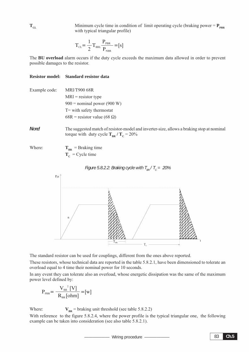
Ch.583—————— Wiring procedure ——————
TCL
Minimum cycle time in condition of limit operating cycle (braking power = PPBR
with typical triangular profile)
T =CL TBRL
PPBR
PNBR
=[s]1
2
The BU overload alarm occurs if the duty cycle exceeds the maximum data allowed in order to preventpossible damages to the resistor.
Resistor model: Standard resistor data
Example code: MRI/T900 68R
MRI = resistor type
900 = nominal power (900 W)
T= with safety thermostat
68R = resistor value (68 Ω)
NOTE! The suggested match of resistor-model and inverter-size, allows a braking stop at nominaltorque with duty cycle T
BR / T
C = 20%
Where: TBR
= Braking time
TC = Cycle time
Figure 5.8.2.2: Braking cycle with TBR / TC = 20%
TC
P,n
TBR
n
t
The standard resistor can be used for couplings, different from the ones above reported.
These resistors, whose technical data are reported in the table 5.8.2.1, have been dimensioned to tolerate anoverload equal to 4 time their nominal power for 10 seconds.
In any event they can tolerate also an overload, whose energetic dissipation was the same of the maximumpower level defined by:
P =PBR
V [V]BR
2
R [ohm]BR
=[w]
Where: VBR
= braking unit threshold (see table 5.8.2.2)
With reference to the figure 5.8.2.4, where the power profile is the typical triangular one, the followingexample can be taken into consideration (see also table 5.8.2.1).
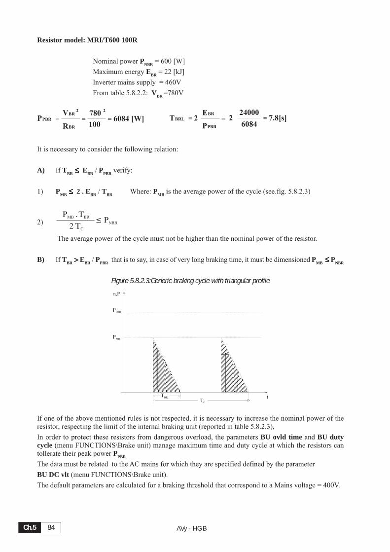
AVy - HGBCh.5 84
Resistor model: MRI/T600 100R
Nominal power PNBR
= 600 [W]
Maximum energy EBR
= 22 [kJ]
Inverter mains supply = 460V
From table 5.8.2.2: VBR
=780V
TBRL = 2EBR
PPBR
=24000
6084= 7.8[s]2PPBR =
VBR
RBR
2
=780
100
2
= 6084 [W]
It is necessary to consider the following relation:
A) If TBR
≤≤≤≤≤ EBR
/ PPBR
verify:
1) PMB ≤≤≤≤≤ 2 . E
BR / T
BRWhere: P
MB is the average power of the cycle (see.fig. 5.8.2.3)
2)P .MB TBR
2 TC
� PNBR
The average power of the cycle must not be higher than the nominal power of the resistor.
B) If TBR
>>>>> EBR
/ PPBR
that is to say, in case of very long braking time, it must be dimensioned PMB
≤ ≤ ≤ ≤ ≤ P
NBR
Figure 5.8.2.3:Generic braking cycle with triangular profile
TC
n,P
PPBR
TBR t
PMB
If one of the above mentioned rules is not respected, it is necessary to increase the nominal power of theresistor, respecting the limit of the internal braking unit (reported in table 5.8.2.3),
In order to protect these resistors from dangerous overload, the parameters BU ovld time and BU dutycycle (menu FUNCTIONS\Brake unit) manage maximum time and duty cycle at which the resistors cantollerate their peak power P
PBR.
The data must be related to the AC mains for which they are specified defined by the parameter
BU DC vlt (menu FUNCTIONS\Brake unit).
The default parameters are calculated for a braking threshold that correspond to a Mains voltage = 400V.
Ch.585—————— Wiring procedure ——————
The use of different braking resistors from those indicated on table 5.8.2.1, requires to take into considera-tion the meaning of following formulas:
BU ovld time [s] = EBR
/ P
PBR (time of braking at limit condition for cycle with triangular profile)
BU duty cycle % = (PNBR
/ PPBR
) x 100
Table 5.8.2.2: Braking thresholds for different Mains
Mains Braking threshold
voltage VBR [V]
230Vac 400
400Vac 680
460Vac / 480 Vac 780avy4200
The result of these calculations must be assigned to the corresponding parameters in menu FUNCTIONS\Brakeunit. When the duty cycle exceeds the data entered, the alarm BU overload automatically occurs in order toprevent possible damages to the resistor.
The following table can be used to choose an external resistor, different from the standard series.
Table 5.8.2.3: Technical data of the internal braking unitsInverter Minimum
type IRMS IPK T RBR
[A] [A] [s] [ohm]
1007
1015
1022
1030
2040
2055
2075
3110 12 22 17 36
3150 17 31 16 26
4185
4220
4300 37 23
4370 29 37
5450
5550
6750
7900
71100
71320
81600
82000 avy4210
67
4.1
6.6
7.8
12
19
16
100
External braking unit (optional)
1078
50 104 22 7.5
18 52 42 15
IRMS
: Nominal current of the braking unit
IPK
: Peak current deliverable for 60 seconds max.
T : Minimum cycle time for a working at IPK
for 10 seconds
Generally the following condition must be satisfed IRMS1 P TPBR BR
R TBR C2
Each drive is provided of the terminals 26 and 27 which allows control of one or more external braking units,parallel connected. The drive will act as Master and the external braking units BU32 must be configured asSlave.
In this way it will be possible to utilize the internal I2x t protection also using external BU (see “AVy-Function description and parameters” instruction manual (available on CD), section 2.15.9 Braking unit).
In case of using more external BUs, each BU with a resistor (all the same) refers to the parameters calcula-tion of a single unit.
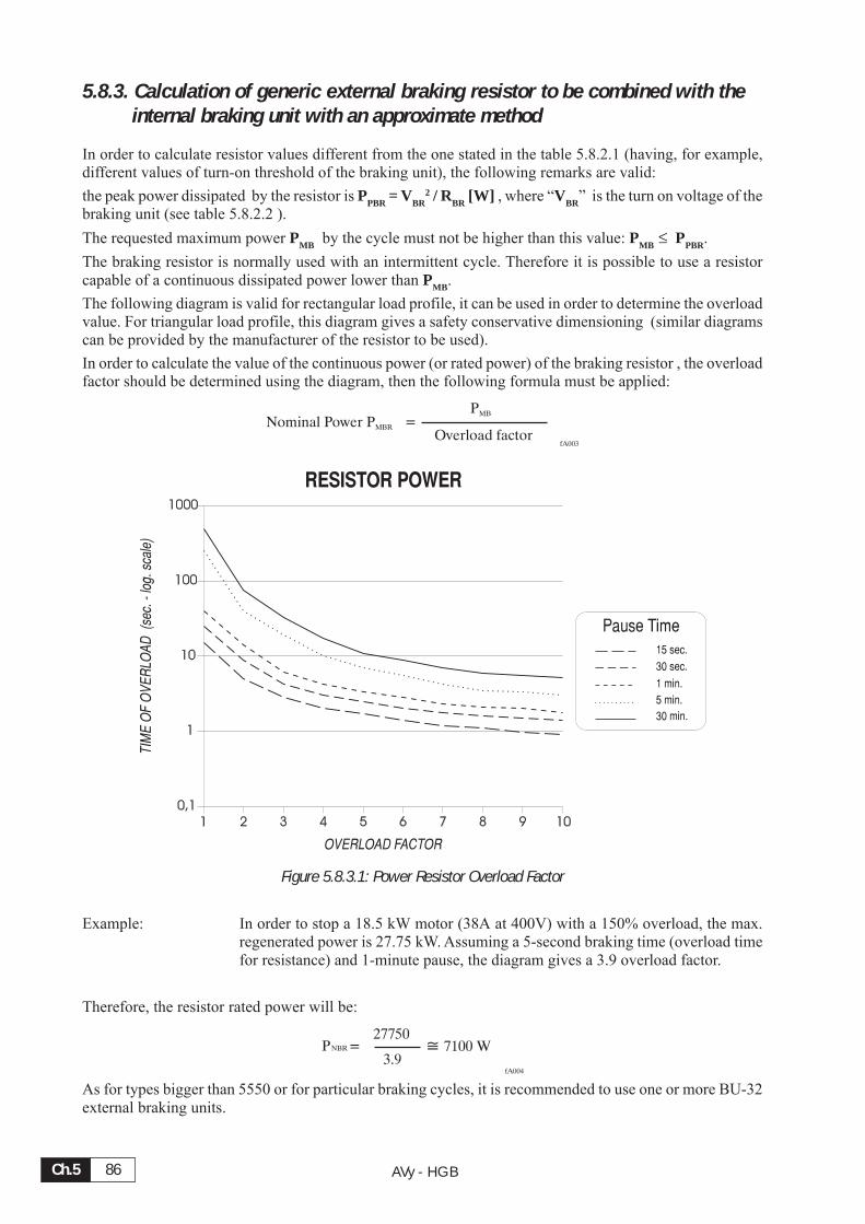
AVy - HGBCh.5 86
5.8.3. Calculation of generic external braking resistor to be combined with theinternal braking unit with an approximate method
In order to calculate resistor values different from the one stated in the table 5.8.2.1 (having, for example,different values of turn-on threshold of the braking unit), the following remarks are valid:
the peak power dissipated by the resistor is PPBR
= VBR
2 / RBR
[W] , where “VBR
” is the turn on voltage of thebraking unit (see table 5.8.2.2 ).
The requested maximum power PMB
by the cycle must not be higher than this value: PMB
≤ PPBR
.
The braking resistor is normally used with an intermittent cycle. Therefore it is possible to use a resistorcapable of a continuous dissipated power lower than P
MB.
The following diagram is valid for rectangular load profile, it can be used in order to determine the overloadvalue. For triangular load profile, this diagram gives a safety conservative dimensioning (similar diagramscan be provided by the manufacturer of the resistor to be used).
In order to calculate the value of the continuous power (or rated power) of the braking resistor , the overloadfactor should be determined using the diagram, then the following formula must be applied:
Nominal Power PMBR =
fA003Overload factor
PMB
RESISTOR POWER
TIM
EO
FO
VE
RLO
AD
(sec
. -lo
g.sc
ale)
OVERLOAD FACTOR
Pause Time
15 sec.
30 sec.
1 min.
5 min.
30 min.
Figure 5.8.3.1: Power Resistor Overload Factor
Example: In order to stop a 18.5 kW motor (38A at 400V) with a 150% overload, the max.regenerated power is 27.75 kW. Assuming a 5-second braking time (overload timefor resistance) and 1-minute pause, the diagram gives a 3.9 overload factor.
Therefore, the resistor rated power will be:
PNBR=
fA004
27750
3.9� 7100 W
As for types bigger than 5550 or for particular braking cycles, it is recommended to use one or more BU-32external braking units.
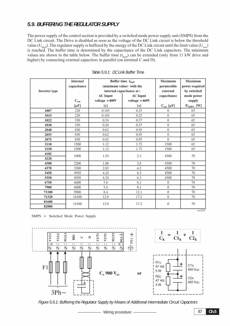
Ch.587—————— Wiring procedure ——————
5.9. BUFFERING THE REGULATOR SUPPLY
The power supply of the control section is provided by a switched mode power supply unit (SMPS) from theDC Link circuit. The Drive is disabled as soon as the voltage of the DC Link circuit is below the thresholdvalue (U
Buff). The regulator supply is buffered by the energy of the DC Link circuit until the limit value (U
min)
is reached. The buffer time is determined by the capacitance of the DC Link capacitors. The minimumvalues are shown in the table below. The buffer time (t
Buff) can be extended (only from 11 kW drive and
higher) by connecting external capacitors in parallel (on terminal C and D).
Table 5.9.1: DC Link Buffer Time
Internal Buffer time tBuff Maximum Maximum
capacitance (minimum value) with the permissible power required
Inverter type internal capacitance at : external by switched
AC Input AC Input capacitance mode power
Cstd voltage =400V voltage =460V supply
[µF] [s] [s] Cext [µF] PSMPS [W]
1007 220 0.165 0.25 0 65
1015 220 0.165 0.25 0 65
1022 330 0.24 0.37 0 65
1030 330 0.24 0.37 0 65
2040 830 0.62 0.95 0 65
2055 830 0.62 0.95 0 65
2075 830 0.62 0.95 0 65
3110 1500 1.12 1.72 1500 65
3150 1500 1.12 1.72 1500 65
4185
4220
4300 2200 1.88 2.8 4500 70
4370 3300 2.83 4.2 4500 70
5450 4950 4.24 6.3 4500 70
5550 4950 4.24 6.3 4500 70
6750 6600 5.6 8.1 0 70
7900 6600 5.6 8.1 0 70
71100 9900 8.4 12.1 0 70
71320 14100 12.8 17.2 0 70
81600
82000avy4220
SMPS = Switched Mode Power Supply
70
14100 12.8 17.2 0 70
1800 1.54 2.3 4500
3Ph~
PE
1/
U1/L
1
V1/L
2
W1/L
3
BR
1
U2/T
1
V2/T
2
W2/T
3
C D
PE
2/
F1
1
Cx
1
C1x
1
C2x= +
C 900 V orX DC
Figure 5.9.1: Buffering the Regulator Supply by Means of Additional Intermediate Circuit Capacitors
AVy - HGBCh.5 88
NOTE! When connecting the intermediate circuit terminals C and D the AC Input side must beprotected with superfast semiconductor fuses!
Formula for calculating the size of the external capacitors:
fA018
Cext =2 P SMPS t Buff 10 6
U2Buff - U2
min
- Cstd
Cext
, Cstd
[μF]
PSMPS
[W] UBuff
= 400 V at ULN
= 400 V
tBuff
[s] UBuff
= 460 V at ULN
= 460 V
UBuff
, Umin
[V] Umin
= 250 V
Calculation example
An AVy4220 Drive is operated with an AC Input supply ULN
= 400 V. A voltage failure buffer is required formax. 1.5 s.
PSMPS
70 W tBuff
1.5 s
UBuff
400 V Umin
250 V
Cstd
1800 μF
C ext =
(400 V) 2 - (250 V) 2- 1800�F = 2154 �F - 1800 �F = 354�F
2 . 70 W . 1.5 s . 10 F / F6�
Ch.589—————— Wiring procedure ——————
5.10. AVy POWER DIP RIDE THROUGH DATA AND RESTART SETUP
The AVy has a 3-phase full-wave rectifier feeding the DC link.
If the DC link reaches the Undervoltage threshold for its voltage input (see tables 5.10.1, 5.10.2 and 5.10.3),the AVy will disable the Drive, and generate an undervoltage alarm.
The undervoltage alarm can latch & trip the drive immediately, or be programmed to reset itself and restart.The undervoltage alarm settings define how many restarts are permitted. There is a ‘restart time’ parameterthat sets how long the undervoltage condition can exist before the AVy gives up on the reset.
The DC link feeds the AVy power supply. If the DC link goes below 250 VDC the electronics reset as if justpowered up. The capacity of the DC link between the undervoltage shutdown of the Drivesection, the 250VDC power supply threshold, and the power draw of the AVy electronics & cooling fan determine how longthe drive stays up under power dips or power loss.
The DC link can have extra capacitance added externally to the DC link to add time to keep the DC linkabove 250 VDC as long as possible. The following tables calculate how long the Drive can keep the powerabove 250 VDC for control power if the maximum amount of capacitance is added externally. Remember,adding capacitance holds in the power supply longer, but also takes longer to recharge.
The survival of an input power dip without shutting down the Drive section depends on the relative load(energy) that the DC bus has to output, and the magnitude and duration of the power dip. A power dip needsto be below the DC undervoltage threshold before the drive would even see any trip condition from it.
Without external capacitors, as an estimate, a power dip of 1 cycle (16.6ms @ 60Hz) when the motor is atfull load will cause an undervoltage trip.
The undervoltage trip time can be calculated by means of the following formula:
fA027t
(U - U ) (C + C )2 2
Buff Std extdc
2Pam
=106
where:
t: undervoltage trip time [ms]
Udc: DC link voltage [V]
Ubuff: trip threshold voltage [V]
CStd
: DC link capacitance [mF]
Cext: external capacitance [mF]
Pam: motor power consumption [W]
Pam depends on the motor load conditions:
- at full load, it can be calculated as follows:
fA028Pam
Pm
�m
=
where:
Pm: motor rated power
ηm: motor rated efficiency
- at no load, it depends on the iron losses, on mechanical losses, and stator joule losses. The sum ofthese terms is about 50% of the full load losses.
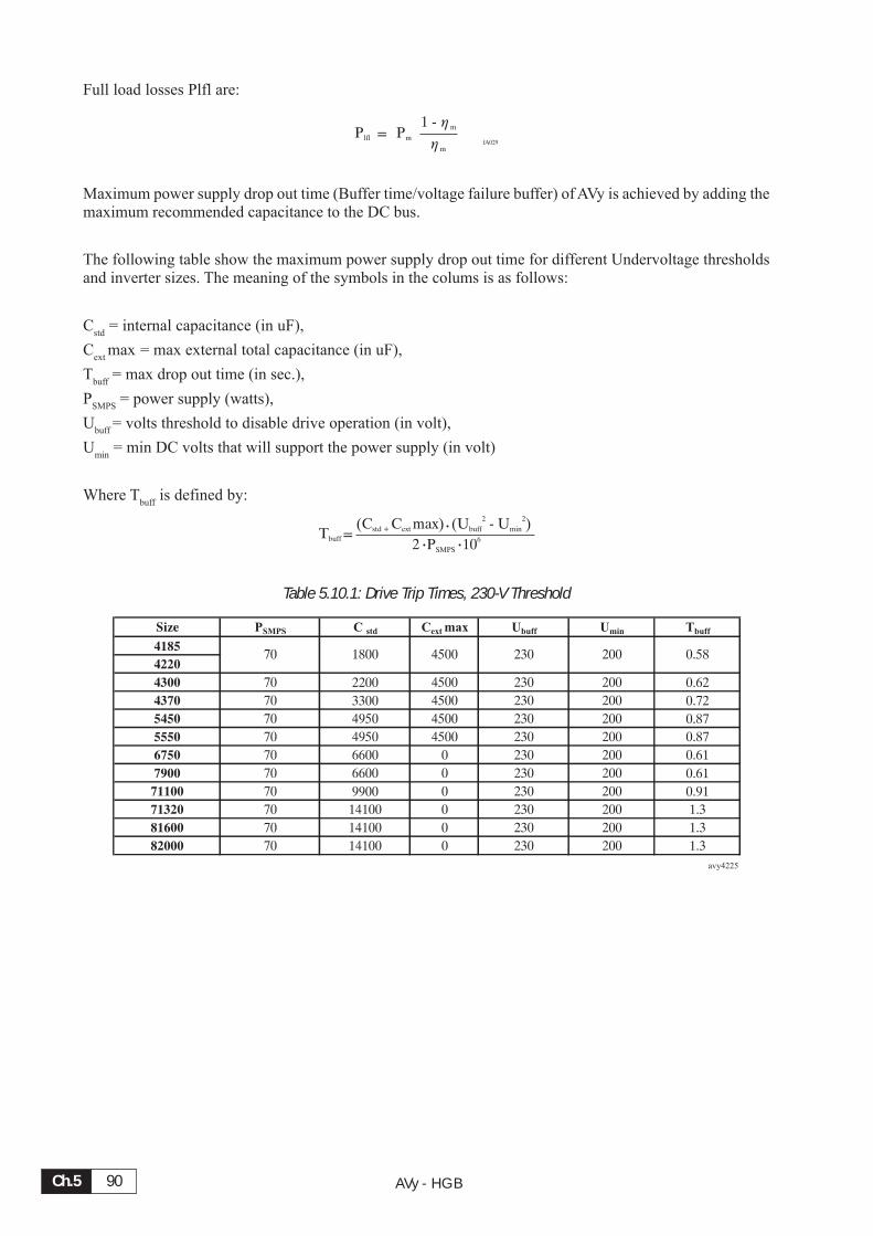
AVy - HGBCh.5 90
Full load losses Plfl are:
fA029Plfl Pm
1 - �m
�m
=
Maximum power supply drop out time (Buffer time/voltage failure buffer) of AVy is achieved by adding themaximum recommended capacitance to the DC bus.
The following table show the maximum power supply drop out time for different Undervoltage thresholdsand inverter sizes. The meaning of the symbols in the colums is as follows:
Cstd
= internal capacitance (in uF),
Cext
max = max external total capacitance (in uF),
Tbuff
= max drop out time (in sec.),
PSMPS
= power supply (watts),
Ubuff
= volts threshold to disable drive operation (in volt),
Umin
= min DC volts that will support the power supply (in volt)
Where Tbuff
is defined by:
Tbuff
(C C max) (U - U )std + ext buff min
2 2
2 P 10SMPS
6=
Table 5.10.1: Drive Trip Times, 230-V Threshold
Size PSMPS C std Cext max Ubuff Umin Tbuff
4185
4220
4300 70 2200 4500 230 200 0.62
4370 70 3300 4500 230 200 0.72
5450 70 4950 4500 230 200 0.87
5550 70 4950 4500 230 200 0.87
6750 70 6600 0 230 200 0.61
7900 70 6600 0 230 200 0.61
71100 70 9900 0 230 200 0.91
71320 70 14100 0 230 200 1.3
81600 70 14100 0 230 200 1.3
82000 70 14100 0 230 200 1.3
avy4225
200 0.5870 1800 4500 230
Ch.591—————— Wiring procedure ——————
Table 5.10.2: Drive Trip Times, 400-V Threshold
Size Psmps C std Cext max Ubuff Umin Tbuff
1007 65 220 0 400 250 0.165
1015 65 220 0 400 250 0.165
1022 65 330 0 400 250 0.24
1030 65 330 0 400 250 0.24
2040 65 830 0 400 250 0.62
2055 65 830 0 400 250 0.62
2075 65 830 0 400 250 0.62
3110 65 1500 1500 400 250 1.12
3150 65 1500 1500 400 250 1.12
4185 70 1800 4500 400 200 1.54
4220 70 1800 4500 400 200 1.54
4300 70 2200 4500 400 200 1.88
4370 70 3300 4500 400 200 2.83
5450 70 4950 4500 400 200 4.24
5550 70 4950 4500 400 200 4.24
6750 70 6600 0 400 200 5.65
7900 70 6600 0 400 200 5.65
71100 70 9900 0 400 200 8.4
71320 70 14100 0 400 200 12.8
81600 70 14100 0 400 200 12.8
82000 70 14100 0 400 200 12.8avy4230
Table 5.10.3: Drive Trip Time, 460-V Threshold
Size Psmps C std Cext max Ubuff Umin Tbuff
1007 65 220 0 460 250 0.25
1015 65 220 0 460 250 0.25
1022 65 330 0 460 250 0.37
1030 65 330 0 460 250 0.37
2040 65 830 0 460 250 0.95
2055 65 830 0 460 250 0.95
2075 65 830 0 460 250 0.95
3110 65 1500 1500 460 250 1.72
3150 65 1500 1500 460 250 1.72
4185 70 1800 4500 460 200 2.3
4220 70 1800 4500 460 200 2.3
4300 70 2200 4500 460 200 2.8
4370 70 3300 4500 460 200 4.2
5450 70 4950 4500 460 200 6.3
5550 70 4950 4500 460 200 6.3
6750 70 6600 0 460 200 8.1
7900 70 6600 0 460 200 8.1
71100 70 9900 0 460 200 12.1
71320 70 14100 0 460 200 17.2
81600 70 14100 0 460 200 17.2
82000 70 14100 0 460 200 17.2avy4240
AVy - HGBCh.5 92
5.11. DISCHARGE TIME OF THE DC-LINK
Table 5.11.1: DC Link Discharge Times
Type I2N Time (seconds) Type I2N Time (seconds)
1007 2.1 4300 58 60
1015 3.5 4370 76 90
1022 4.9 5450 90
1030 6.5 5550 110
2040 8.3 6750 142
2055 11 7900 180
2075 15.4 71100 210
3110 21.6 71320 250
3150 28.7 81600 310
4185 35,5 60 82000 365 120
4220 42 60 avy4250
120
90
150
205
220
This is the minimum time that must be elapsed since an AVy Drive is disconnected from the AC Input beforean operator may service parts inside the Drive to avoid electric shock hazard.
CONDITION These values consider a turn off for a Drive supplied at 480Vac +10%, without any option, ( thecharge for the switching supply is the regulation card, the keypad and the 24Vdc fans “ifmounted”).
The Drive is disabled. This represents the worst case condition.
Ch.693——— Maintenance ———
6. MAINTENANCE
6.1. CARE
The SieiDrive - AVy inverters must be installedaccording to the relevant installation regulations.They do not require any particular maintenance. Theyshould not be cleaned with a wet or moist cloth. Thepower supply must be switched off before cleaning.
6.2. SERVICE
The screws of all terminals on the device should bere-tightened two weeks after initial commissioning.This should be repeated each year.
If the drives have been stored for more than threeyears, the capacitance of the intermediate circuitcapacitors may have been impaired. Beforecommissioning these devices, it is advisable toregenerate the capacitors by connecting them to thevoltage for two hours with the inverter disabled. Afterthese operations the device is ready to be installedwithout limitations.
6.3. REPAIRS
Repairs of the device should only be carried out bythe specialist personnel (qualified by the manufac-turer)
If you carry out a repair on your own, observe thefollowing points:
- When ordering spare parts do not only state thedevice type but also the device serial number(nameplate). It is also useful to state the type ofthe regulator card and the version of the operatingsystem (on Firmware & Card revision levelnameplate, see figure 3.1.3.2).
- When exchanging cards ensure that the positionsof switches and jumpers are observed! This par-ticularly applies to switch S3 on the regulationcard.
NOTE! The manufacturer does not acceptany liability for any device partsthat are destroyed due to the in-correct switch position of "switchS3".
6.4. CUSTOMER SERVICE
For customer service, please contact your Gefranoffice.
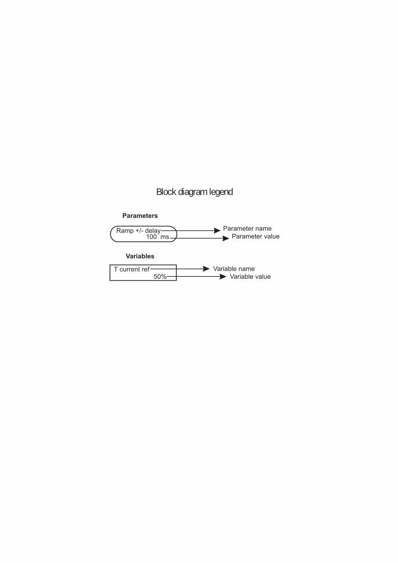
Block diagram legend
Ramp +/- delay100 ms
T current ref50%
Parameter name
Variable name
Parameter value
Variable value
Parameters
Variables
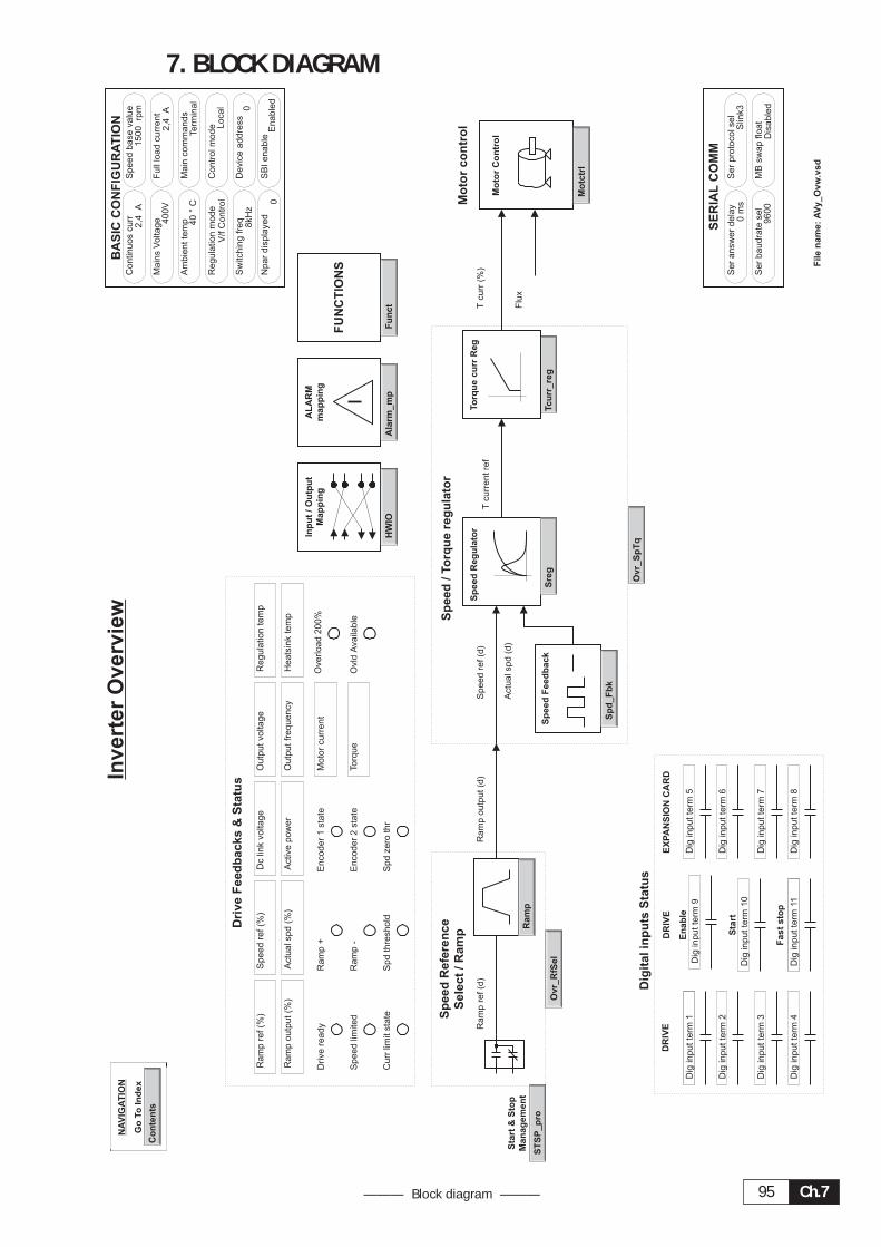
Ch.795——— Block diagram ———
7. BLOCK DIAGRAM
Inve
rte
rO
ve
rv
iew
Sp
eed
Re
feren
ce
Se
lec
t/
Ra
mp
Mo
tor
Co
ntr
ol
Inp
ut
/O
utp
ut
Ma
pp
ing
HW
IO
Sp
ee
dR
eg
ula
tor
Sp
ee
dF
ee
db
ac
k
Sp
eed
/To
rq
ue
re
gu
lato
r
FU
NC
TIO
NS
Fu
nct
Driv
eF
eed
bac
ks
&S
tatu
s
Sre
g
Ra
mp
Ov
r_
RfS
el
Ov
r_
Sp
Tq
Sp
d_
Fb
k
Tc
urr_
re
g
Mo
tctr
l
Co
nte
nts
Go
To
Ind
ex
NA
VIG
AT
ION
To
rq
ue
cu
rr
Re
g
Ala
rm
_m
p
AL
AR
M
ma
pp
ing
BA
SIC
CO
NF
IGU
RA
TIO
N
Dig
ital
inp
uts
Sta
tus
DR
IVE
DR
IVE
Mo
tor
co
ntr
ol
ST
SP
_p
ro
Sta
rt
&S
top
Ma
na
ge
men
t
En
ab
le
Sta
rt
Fast
sto
p
EX
PA
NS
ION
CA
RD
Ram
pre
f(d
)S
peed
ref(d
)T
curr
entre
f
Flu
x
Ram
poutp
ut(d
)
Actu
alspd
(%)
Outp
utfr
equency
Dc
link
voltage
Ram
pre
f(%
)
Active
pow
er
Actu
alspd
(d)
Drive
ready
Encoder
1sta
teR
am
p+
Speed
limited
Ram
p-
Spd
zero
thr
Encoder
2sta
te
Curr
limit
sta
te
Torq
ue
Ram
poutp
ut(%
)
Outp
utvoltage
Speed
ref(%
)R
egula
tion
tem
p
Heats
ink
tem
p
Moto
rcurr
ent
Ovld
Availa
ble
Spd
thre
shold
Tcurr
(%)
Main
sV
oltage 400V
Am
bie
ntte
mp 40
°C
Regula
tion
mode
V/f
Contr
ol
Dig
inputte
rm1
Dig
inputte
rm2
Dig
inputte
rm3
Dig
inputte
rm4
Dig
inputte
rm5
Dig
inputte
rm6
Dig
inputte
rm7
Dig
inputte
rm8
Sw
itchin
gfr
eq
8kH
z
Speed
base
valu
e1500
rpm
Full
load
curr
ent
2,4
A
Main
com
mands
Term
inal
Contr
olm
ode L
ocal
Devic
eaddre
ss
0
Overload
200%
Continuos
curr
2,4
A
Dig
inputte
rm9
Dig
inputte
rm10
Dig
inputte
rm11
Fil
en
am
e:
AV
y_
Ov
w.v
sd
Npar
dis
pla
yed
0S
BIenable
Enable
d
SE
RIA
LC
OM
M
Ser
baudra
tesel
9600
Ser
pro
tocolsel
Slin
k3
MB
sw
ap
float
Dis
able
d
Ser
answ
er
dela
y0
ms
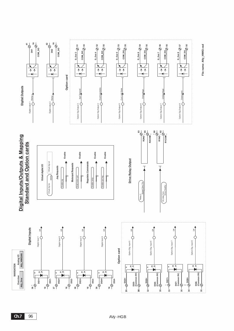
AVy -HGBCh.7 96
Dig
italIn
pu
ts/O
utp
uts
&M
ap
pin
g
Sta
nd
ard
an
dO
pti
on
card
s
AV
y_O
vw
Overvie
wNA
VIG
AT
ION
Dig
ita
lIn
pu
ts
AV
y_H
WIO
AN
An
alo
gI/O
*
DG
1-
16
DG
1+
36
*
DG
2-
16
DG
2+
37
*
DG
3-
16
DG
3+
38
*
DG
4-
16
DG
4+
39
*
DG
5-
(Co
mm
on
0V
)
DG
5+
*
DG
6-
(Co
mm
on
0V
)
DG
6+
*
DG
7-
Co
mm
on
0V
)
DG
7+
DG
8-
(Co
mm
on
0V
)
DG
8+
Driv
eR
ela
yO
utp
ut
D02
42
CO
M_D
O
16
D_O
ut
3
CO
M_D
O
D_O
ut
4
CO
M_D
O
D_O
ut
5
CO
M_D
O
D_O
ut
6
CO
M_D
O
D_O
ut
7
CO
M_D
O
D_O
ut
8
CO
M_D
O
R2N
O
83
R2C
OM
85
D01
41
CO
M_D
O
16
Dig
ita
lO
utp
uts
R1N
O
80
R1C
OM
82
Op
tio
nc
ard
Op
tio
nc
ard
Jo
gR
eq
uests
Reg
ula
tor
Co
mm
an
ds
Mo
torp
ot
Req
uests
T T TT
En
ab
le
En
ab
le
En
ab
le
En
ab
le
Vir
tuald
igit
alI/O
Dig
ita
lin
pu
t1
Off
Op
tio
nD
ig.
inp
ut8
Off
Dig
ita
lin
pu
t2
Off
Dig
ita
lin
pu
t3
Off
Dig
ita
lin
pu
t4
Off
Op
tio
nD
ig.
inp
ut
5O
ff
Op
tio
nD
ig.
inp
ut6
Off
Op
tio
nD
ig.
inp
ut7
Off
Ok
rela
yfu
nc.
Drive
He
alth
y
Re
lay
2 Sp
ee
dZ
ero
Th
r
Dig
ita
lo
utp
ut
1R
am
p+
Dig
ita
lo
utp
ut
2R
am
p-
Op
tio
nD
ig.O
utp
ut
3S
pd
Th
resold
Op
tio
nD
ig.O
utp
ut4
Ove
rld
Ava
ilab
le
Op
tio
nD
ig.O
utp
ut5
Cu
rrLim
itS
tate
Op
tio
nD
ig.O
utp
ut6
Ove
rvolta
ge
Op
tio
nD
ig.O
utp
ut7
Un
de
rvolta
ge
Op
tio
nD
ig.O
utp
ut8
Ove
rcu
rre
nt
En
ab
lejo
g
En
ab
mo
tor
po
t
En
ab
lesp
dre
g
En
ab
lera
mp
Virtu
ald
igo
ut
Virtu
ald
igin
p0
00
0h
31
35
32
35
33
35
34
35
31
35
51
55
52
55
53
55
54
55
56
55
57
55
Fil
en
am
e:
AV
y_
HW
IO.v
sd

Ch.797——— Block diagram ———
An
alo
gIn
pu
ts/O
utp
uts
&M
ap
pin
gA
na
log
Ou
tpu
ts
22
21
D A C 1
2223
D A C 2
AO
1
AC
OM
AO
2
AC
OM
12
11
D A C 1
AO
3
AC
OM
14
13
D A C 2
AO
4
AC
OM
�+
-65
Vo
lts
Ref_
3-
Ref_
3+
HW
inp
ut
typ
e
S+
-43
Vo
lts
Ref_
2-
Ref_
2+
HW
inp
ut
typ
e
AV
y_O
vw
Overvie
wNA
VIG
AT
ION
AV
y_H
WIO
Dig
italI/
O
�+
-21
Vo
lts
Ref_
1-
Ref_
1+
HW
inp
ut
typ
e
Win
do
wco
mp
arato
r
F
F
F
Op
tio
nc
ard
65 18 97
A+
A-
B+
B-
0V
5V
XE
co
nn
ec
tor
65 18 2/9
7
A+
A-
B+
B-
0V
+V
XF
Ic
on
ne
cto
r
En
co
de
r1
En
co
de
r2
(Op
tio
n)
Tach
follo
wer
Fro
md
igit
alrefe
re
nc
e
sett
ing
Fro
md
igit
alrefe
re
nc
e
sett
ing
Fro
md
igit
alrefe
re
nc
e
sett
ing
Sele
ctoutp
ut1
1
Actu
alS
pd
(rpm
)
Sele
ctoutp
ut2
Torq
ue
Curr
ent
Scale
outp
ut1
1
Scale
outp
ut2
Sele
ctoutp
ut3
Curr
entU
Scale
outp
ut3
1
Sele
ctoutp
ut4
Moto
rC
urr
ent
Scale
outp
ut4
1
Input3
type -1
0V
...+
10V
Offsetin
put3
0
Scale
input3
1
Tune
valu
ein
p3
1
Sele
ctin
put3
Off
Input2
type -1
0V
...+
10V
Offsetin
put2
0
Scale
input2
1
Tune
valu
ein
p2
1
Sele
ctin
put2
Off
Auto
tune
inp
30
Auto
tune
inp
20
Input1
type -1
0V
...+
10V
Offsetin
put1
0
Scale
input1
1
Tune
valu
ein
p1
1A
uto
tune
inp
10
Input1
filter
0m
s
Sele
ctin
put1
Ram
pR
ef1
Input1
com
pare
0
Input1
cp
err
or
0
Input1
cp
dela
y0
ms
Input1
cp
matc
hAn
in1
targ
et
An
in2
targ
et
An
in3
targ
et
Sele
ctenc
2O
FF
Sele
ctenc
1O
FF
Sele
ctin
put1
Ram
pR
ef1
Sele
ctin
put2
Off
Sele
ctin
put3
Off
�
Fil
en
am
e:
AV
y_H
WIO
AN
.vsd
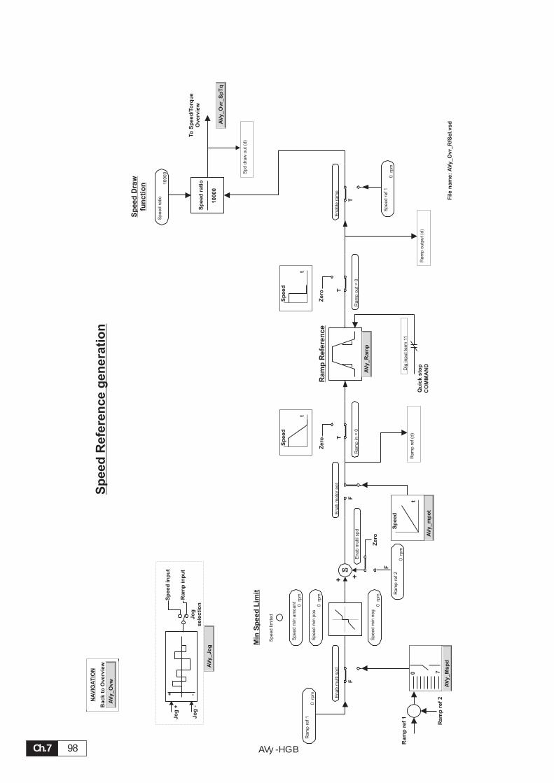
AVy -HGBCh.7 98
Sp
ee
dR
efe
re
nc
eg
en
era
tio
nA
Vy_O
vw
Back
toO
vervie
w
NA
VIG
AT
ION
AV
y_O
vr_S
pT
q
To
Sp
eed
/To
rq
ue
Overvie
wS
peed
rati
o
10000
FF
Min
Sp
ee
dL
imit
S+ +
AV
y_m
po
t
T
Ra
mp
Re
fere
nc
e
AV
y_R
am
p
Zero
T
Zero
T
+ -
Jo
g+
Jo
g-
Ram
pin
pu
t
Sp
eed
inp
ut
Jo
g
sele
cti
on
AV
y_Jo
g
Sp
eed
tt
Sp
eed
t
Sp
eed
Sp
ee
dD
ra
w
fun
cti
on
Qu
ick
sto
p
CO
MM
AN
D
0 7
AV
y_M
sp
d
Ram
pref
1
Ram
pref
2
Sp
ee
dra
tio
10
00
0 Sp
dd
raw
ou
t(d
)
En
ab
mo
tor
po
tE
na
bm
ultisp
d
Sp
ee
dm
ina
mo
un
t0
rpm
Sp
ee
dm
inp
os
0rp
m
Sp
ee
dm
inn
eg
0rp
m
Ra
mp
in=
0R
am
po
ut
=0
En
ab
lera
mp
Sp
ee
dre
f1
0rp
m
Ra
mp
ref
10
rpm
Ra
mp
ref
20
rpm
Ra
mp
ref
(d)
Sp
ee
dlim
ite
d
Ra
mp
ou
tpu
t(d
)
Dig
inp
ut
term
11
�
File
nam
e:
AV
y_O
vr_R
fSel.v
sd
Zero
F
En
ab
mu
ltisp
d
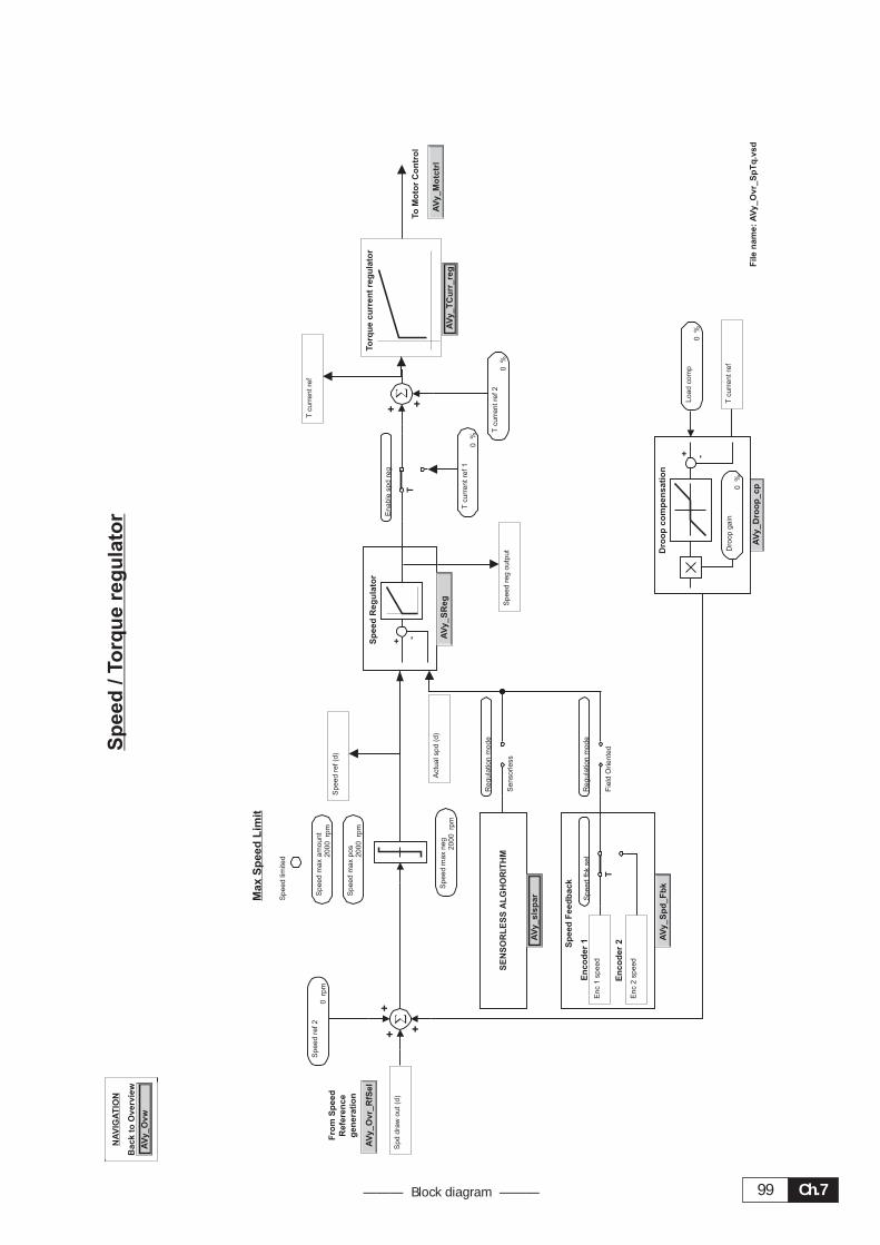
Ch.799——— Block diagram ———
Sp
ee
d/
To
rq
ue
reg
ula
tor
AV
y_O
vw
Back
toO
vervie
w
NA
VIG
AT
ION
Sp
ee
dF
ee
db
ack
-
+Sp
ee
dR
eg
ula
tor
AV
y_S
Reg
AV
y_O
vr_R
fSel
Fro
mS
pee
d
Refe
re
nc
e
gen
erati
on
AV
y_D
ro
op
_cp
+ +
+
En
co
der
1
-+
AV
y_S
pd
_F
bk
En
co
der
2
T
T
AV
y_M
otc
trl
To
Mo
tor
Co
ntr
ol
AV
y_T
Cu
rr_re
g
To
rq
ue
cu
rre
nt
re
gu
lato
r
+ +
Ma
xS
pe
ed
Lim
it
Dro
op
co
mp
en
sati
on
SE
NS
OR
LE
SS
AL
GH
OR
ITH
M
AV
y_
sls
par
Enc
1speed
Enc
2speed
Dro
op
ga
in0
%
Speed
max
am
ount
2000
rpm
Speed
max
pos
2000
rpm
Speed
max
neg
2000
rpm
Speed
ref2
0rp
m
Speed
reg
outp
ut
Speed
fbk
sel
Enable
spd
reg
Tcurr
entre
f1
0%
Tcurr
entre
f2
0%
Tcurr
entre
f
Load
com
p0
%
Spd
dra
wout(d
)
Speed
ref(d
)
Actu
alspd
(d)
Tcurr
entre
f
Speed
limited
Regula
tion
mode
Fie
ldO
riente
d
Regula
tion
mode
Sensorless
Fil
en
am
e:
AV
y_
Ov
r_
Sp
Tq
.vs
d
AVy -HGBCh.7 100
Ra
mp
re
feren
ce
Blo
ck
Mu
ltiR
am
pF
un
cti
on
Sp
ee
d
t
Qu
ick
sto
p
F
AV
y_O
vr_R
fSel
Back
NA
VIG
AT
ION
Refe
re
nc
eR
am
pA
Vy_S
re
g
To
Sp
ee
dR
efe
re
nc
e
gen
erati
on
F
Lin
ear
S-s
hap
e
S-s
hap
eT
0t
Lin
ear
T Free
ze
ram
p
CO
MM
AN
D
Fro
m
Ram
pin
=0
To
Ram
po
ut=
0
Acc
de
lta
sp
ee
d1
10
0rp
mD
ec
de
lta
sp
ee
d1
10
0rp
m
Acc
de
lta
sp
ee
d1
00
rpm
De
cd
elta
sp
ee
d1
00
rpm
Acc
de
lta
sp
ee
d2
10
0rp
mD
ec
de
lta
sp
ee
d2
10
0rp
m
Acc
de
lta
tim
e1
s
De
cd
elta
tim
e1
s
QS
tpd
elta
sp
ee
d1
00
0rp
m
En
ab
mu
ltirm
p
QS
tpd
elta
tim
e1
s
Acc
de
lta
sp
ee
d0
10
0rp
m
Acc
de
lta
sp
ee
d3
10
0rp
m
De
cd
elta
sp
ee
d0
10
0rp
m
De
cd
elta
sp
ee
d3
10
0rp
m
Acc
de
lta
tim
e0
1s
Acc
de
lta
tim
e1
1s
Acc
de
lta
tim
e2
1s
Acc
de
lta
tim
e3
1s
De
cd
elta
tim
e0
1s
De
cd
elta
tim
e1
1s
De
cd
elta
tim
e2
1s
De
cd
elta
tim
e3
1s
Sa
cc
tco
nst
05
00
ms
Sa
cc
tco
nst
15
00
ms
Sa
cc
tco
nst
25
00
ms
Sa
cc
tco
nst
35
00
ms
Sd
ec
tco
nst
05
00
ms
Sd
ec
tco
nst
15
00
ms
Sd
ec
tco
nst
25
00
ms
Sd
ec
tco
nst
35
00
ms
Ra
mp
ref
(d)
Ra
mp
sh
ap
e
Ssh
ap
et
co
nst 50
0m
s
Sa
cc
tco
nst
50
0m
s
Sd
ec
tco
nst
50
0m
s
Ra
mp
sh
ap
e
Ramp
+
Ra
mp
-
Ra
mp
+/-
de
lay 1
00
ms
Fre
eze
ram
p
Fil
en
am
e:
AV
y_R
am
p.v
sd
Ch.7101——— Block diagram ———
Sp
ee
dre
gu
lato
r
AV
y_
Ovr_
Sp
Tq
Ba
ck
NA
VIG
AT
ION
Sp
ee
dA
dap
tive
an
d
Sp
ee
dzero
log
ic
P/I
sp
eed
reg
ula
tor
�+ +
�+ +
+
AV
y_
Srp
i
Sp
eed
up
AV
y_
J_
co
mp
AV
y_
Dro
op
_c
p
Ine
rti
a/L
os
sc
om
p
Sp
eed
dro
op
co
mp
�+ +
AV
y_
Sp
d_
fbk
AV
y_
Ad
p_s
pd
Sp
ee
dP
/Ib
ase
valu
e
Sp
eed
fbk
T
AV
y_
Tc
urr_reg
To
To
rq
ue
cu
rren
t
reg
ula
tor
FT
�+
+
Ze
ro
�+ +
Sp
ee
dL
imit
s
Lo
ad
co
mp
T
Ze
ro
torq
ue
CO
MM
AN
D
P/I
reg
ula
tor
inc
lud
es
an
ti-w
ind
up
log
ic
F
Tcurrent
ref
2
0%
Tcurrent
ref1
0%
Speed
reg
output
Speed
ref
1 0rpm
Speed
ref
2 0rpm
Speed
ref
(d)
Actual
spd
(rpm)
Speed
up
gain 0
%
Speed
up
filter
0ms
Speed
up
base
1000
ms
Speed
Pin
use
Speed
Iin
use
Speed
P
10
%
Speed
I
1%
Prop.
filter 0
ms
Lock
speed
I
Not
Active
Speed
Pbase
0.939379
A/rpm
Speed
Ibase
0.234845
A/rpm*ms
Aux
spd
fun
sel
Speed
min
pos
0rpm
Speed
min
neg
0rpm
Speed
min
amount
0rpm
Speed
max
pos
5000
rpm
Speed
max
neg
5000
rpm
Speed
max
amount
5000
rpm
Lock
speed
reg
Enable
spd
reg
Zero
Torque
Tcurrent
ref
Aux
spd
fun
sel
�
�
�
Fil
en
am
e:
AV
y_
Sreg
.vs
d
AVy -HGBCh.7 102
Sp
ee
dre
gu
lato
rP
Ip
art
+ +
+ +
He
re
the
co
ntr
ibu
tio
n
du
eto
the
sp
ee
du
pp
art
isn
ot
sh
ow
n
Ze
ro
AV
y_
Sre
g
Ba
ck
toO
ve
rv
iew
NA
VIG
AT
ION
T
F
Ze
ro
F
Ad
ap
Ig
ain
s
Sp
ee
dA
da
pti
ve
an
d
Sp
ee
dze
ro
log
ic
Ad
ap
re
fere
nc
eA
da
pI
ga
ins
Ad
ap
Pg
ain
s
F
Ad
ap
Pg
ain
s
AV
y_
Ad
p_
sp
d
An
ti-w
ind
up
To
rq
ue
cu
rre
nt
lim
its
An
ti-w
ind
up
Sp
ee
dre
f(d
)
Actu
alsp
d(r
pm
)
Sp
ee
dP
inu
se
Sp
ee
dI
inu
se
Sp
ee
dre
go
utp
ut
Pro
p.
filte
r0
ms
Lo
ck
sp
ee
dI
Lo
ck
sp
ee
dre
g
En
able
sp
da
da
p
Sp
ee
dI
1%
En
able
sp
da
da
p
Sp
ee
dP
10
%
��
Ch.7103——— Block diagram ———
Dro
op
co
mp
en
sa
tio
n
AV
y_S
reg
Back
NA
VIG
AT
ION
-+
low
pass
filter
Zero
T
To
Sp
eed
refe
ren
ce
Tcu
rre
nt
ref
Lo
ad
co
mp
0%
Dro
op
limit
15
00
rpm
Dro
op
filte
r0
ms
Dro
op
gain
0%
En
able
dro
op
�
Fil
en
am
e:
AV
y_D
ro
op
_cp
.vsd
AVy -HGBCh.7 104
Ine
rti
a/L
os
sc
om
pe
ns
ati
on
n
d
low
pass
filter
AV
y_
Sre
g
Ba
ck
NA
VIG
AT
ION
Sp
ee
d
+1
To
sp
ee
dre
gu
lato
r
ou
tpu
t
T
Speed
ref(d
)
Ref0
level
10
rpm
Inert
iac
filter
0m
s
Flu
xre
fere
nce
Inert
ia0.0
05
Kg*m
*m
Friction
0.0
01
N*m
Torq
ue
const
Aux
spd
fun
se
l
Fil
en
am
e:
AV
y_
J_
co
mp
.vs
d
Ch.7105——— Block diagram ———
Fil
en
am
e:
AV
i_Tcu
rr_re
g.v
sd
To
rq
ue
cu
rren
treg
ula
tor
Mo
torin
g&
Gen
erati
ng
To
rq
ue
Lim
it
Fro
mS
pee
dR
eg
ula
tor
AV
y_O
vr_S
pT
q
Back
toO
vervie
w
NA
VIG
AT
ION
AV
y_S
Reg
AV
y_
mo
tctr
l
To
Mo
tor
Co
ntr
ol
To
Dro
op
Fee
db
ack
AV
y_D
ro
op
_cp
Cu
rren
treg
P/I
base
valu
e
speed
torq
ue
Tcu
rren
tlim
+
Tcurr
ent
lim-
Tcurr
ent
lim-
Tcu
rren
tlim
+
+1%
of
Moto
rnom
speed
-1%
of
Moto
rnom
speed
OV
ER
LO
AD
Co
ntr
ol
I2t
DR
IVE
MO
TO
R
To
rq
ue
cu
rren
tlim
its
To
rq
ue
re
du
cti
on
+
speed
torq
ue
Tcu
rren
tlim
+
Tcurr
ent
lim-
Tcurr
ent
lim-
Tcu
rren
tlim
+
T
P/I
reg
ula
tor
inclu
des
an
ti-w
ind
up
log
ic
T
To
rq
ue
red
uc
tio
n
CO
MM
AN
D
To
rq
ue
Lim
it+
/-
Tcu
rre
ntlim
+1
36
%
Tcu
rre
ntlim
-1
36
%
Tcu
rre
ntlim
13
6%
Inu
se
Tcu
rlim
+
Inu
se
Tcu
rlim
-
Cu
rre
nt
P6
.1%
Cu
rre
ntI
0.6
%
Cu
rre
nt
Pb
ase
47
5.5
18
V/A
Cu
rre
ntI
ba
se
47
5.5
18
V/A
*ms
Cu
rre
ntlim
red
10
0%
I_sq
rt_
t_a
ccu
m
Ovld
Ava
ilab
le
Mo
tor
co
nt
cu
rr1
00
%
Trip
tim
e5
0%
60
s
Tcurrent
ref
To
rqu
ecu
rre
nt
Ovld
mo
tsta
te
Cu
rrlim
itsta
te
Tcu
rrlim
typ
e
To
rqu
ere
du
ct.
Ove
rlo
ad
20
0%
AVy -HGBCh.7 106
Sp
eed
Feed
back
AV
y_
Ovr_
Sp
Tq
Ba
ck
toO
ve
rv
iew
NA
VIG
AT
ION
Mo
tor
En
co
de
rS
etu
p
Sp
eed
En
co
de
r1
(Sin
us
oid
al
or
Dig
ita
l)
T
Ind
ex
Sto
rin
g
AV
y_m
otc
trl
Go
tom
oto
rc
on
tro
l
OP
TIO
N
En
co
de
rrep
ea
ter
(OP
TIO
N)
XE
1c
on
ne
cto
r
En
co
de
r1
65 18 43
A+
A-
B+
B-
C+
C-
0V
5V
97
65 18 43
A+
A-
B+
B-
C+
C-
0V
+V
2/97
XF
Ic
on
ne
cto
r
En
co
de
r2
T
Encoder
1ty
pe
Dig
ital
Encoder
1pu
lses
1024
Encoder
2pu
lses
1024
Refr
esh
enc
1D
isable
d
Refr
esh
enc
2D
isable
d
Enab
lein
dsto
re Dis
ab
led
Speed
fbk
se
l
Actu
alspd
(d)
Enc1
supp
lyvlt
5.4
1V
Encoder
repeat
File
na
me:
AV
y_
sp
d_
fbk
.vsd
Ch.7107——— Block diagram ———
Mo
tor
co
ntr
ol
Flu
xreg
ula
tor
Vo
ltag
ereg
ula
tor
Flu
xcu
rre
nt
reg
ula
tor
RE
GU
LA
TIO
N
Flu
xm
od
el
++
+
Vo
ltag
elim
it
AC
Mo
tor
En
co
de
r
(op
tio
n)
Vo
lta
ge
re
gb
as
ev
alu
eF
lux
re
gb
as
ev
alu
e
Flu
xm
ax
(ram
ped)
Flu
xm
in
AV
y_sp
d_fb
k
AV
y_O
vw
Back
toO
vervie
w
NA
VIG
AT
ION
AV
y_m
otp
ar
AV
y_O
vr_S
pT
q
Fro
mS
peed
/To
rq
ue
reg
ula
tor
AV
y_sls
par
T
Flu
xm
ax
(ram
ped)
CO
NF
IGU
RA
TIO
N
Flu
xm
od
el
Flu
xm
ax
PW
M
Mag
neti
zati
on
log
ic
Flu
xm
ax
(ram
ped)
Flu
xcu
rre
nt
lim
it
P/I
reg
ula
tors
inclu
de
an
ti-w
ind
up
log
ic
AV
y_m
otp
ar
Go
toM
oto
r
param
ete
rs
Go
toM
oto
r
param
ete
rs
Go
toS
en
so
rle
ss
param
ete
rs
Ou
tvlt
leve
l1
00
%
Dc
link
vo
lta
ge
Flu
xle
ve
l1
00
%
Ba
se
vo
lta
ge
46
0V
Ba
se
fre
qu
en
cy
60
Hz
Ro
tor
resis
tan
ce
1.0
75
85
Oh
m
P1
flu
xm
od
el
0.4
5
P2
flu
xm
od
el
9
Sta
tor
resis
t1
.07
58
5O
hm
Ma
gn
etizin
gcu
rr2
.33
27
6A
Lkg
ind
ucta
nce
0.0
31
70
09
H
Flu
xcu
rre
nt
Flu
x
Ou
tpu
tvo
lta
ge
Dyn
am
vlt
ma
rgin
1%
Vo
lta
ge
P1
5%
Vo
lta
ge
I4
%
Flu
xP
6%
Flu
xI
1.4
%Vo
lta
ge
Pb
ase
0.0
05
26
42
8V
s/V
Vo
lta
ge
Ib
ase
0.6
58
03
5V
s/V
*s
Flu
xP
ba
se
85
5.0
43
A/V
s
Flu
xI
Ba
se
7.5
15
03
A/V
s*m
s
Flu
xre
fere
nce
Fcu
rre
nt
ref
Flu
xre
gm
od
e
To
rqu
ecu
rre
nt
Ba
se
vo
lta
ge
46
0V
File
nam
e:
AV
y_m
otc
trl.v
sd
AVy -HGBCh.7 108
Mo
tor
pa
ra
me
ters
f
V
AV
y_O
vw
Back
toO
vervie
w
NA
VIG
AT
ION
AV
y_
mo
tctr
l
Back
tom
ot
ctr
l
LS
LR
LS
+L
R
Flu
xre
f
t
Flu
xre
f
t
Dyn
am
ic
CE
MF
Flu
xcurr
ent
Flu
x
Mag
neti
zati
on
init
log
ic
min
Flu
xm
ax
(ram
ped)
T
En
ab
lerr
ad
ap
.
No
min
alvo
lta
ge
46
0V
No
min
alsp
ee
d1
76
5rp
m
No
mfr
eq
ue
ncy
60
Hz
No
min
alcu
rre
nt
4.8
A
Co
sp
hi
0.8
1
Ba
se
vo
lta
ge
46
0V
Ba
se
fre
qu
en
cy
60
Hz
Ma
gn
etizin
gcu
rr2
.33
27
6A
Sta
tor
resis
t1
.07
58
5O
hm
Ro
tor
resis
tan
ce
1.0
75
85
Oh
m
Lkg
ind
ucta
nce
0.0
31
70
09
H
Ma
gn
ram
ptim
e1
s
Ma
gn
bo
ost
cu
rr.
30
%
Fil
en
am
e:
AV
y_
mo
tpar.
vsd
Ch.7109——— Block diagram ———
SE
NS
OR
LE
SS
Param
ete
rs
Flu
xm
od
el
Esti
mate
dsp
ee
d
for
Sen
so
rle
ss
mo
de
IM
ag
n
Flu
x
Wo
rkin
g
Flu
x
AV
y_O
vw
Overvie
wNA
VIG
AT
ION AV
y_
mo
tctr
l
Back
toM
ot
co
ntr
ol
De
ad
tim
ec
om
pe
ns
ati
on
Ac
tualsp
ee
d
Ou
tpu
tvo
ltag
e
Vo
ltag
eco
mm
an
d
toP
WM
Low
speed
facto
r5000
Sls
speed
filter
0.0
1s
Flu
xcorr
facto
r0.9
Magn
work
ing
cur
Regula
tion
mode
V/f
Contr
ol
Com
pslo
pe
13
V/A
Voltage
com
plim
6V
Fil
en
am
e:
AV
y_
sls
par.
vsd
AVy -HGBCh.7 110
V/H
zfu
nc
tio
ns
Vo
ut
f
EN
ER
GY
SA
VE
Vo
ltag
eB
oo
st
AV
y_O
vw
Overvie
wNA
VIG
AT
ION
AV
y_F
un
ct
Go
tofu
ncti
on
s
Slip
Co
mp
en
sati
on
To
rq
ue
Sp
ee
d
V
f
V/f
sh
ap
e
V/f
sp
eed
searchT
En
ab
le
Ba
se
volta
ge
460
V
Ba
se
freq
ue
ncy
60
Hz
V/f
sh
ap
eV
=k
*f
1.0
Vlt
bo
ost
typ
eM
an
ual
Ma
nu
alb
oo
st
1%
Slip
co
mp
typ
eM
an
ual
Ma
nu
alslip
co
mp 0
rpm
Slip
co
mp
filt
0.0
3s
Flu
xva
rtim
e1
0s
En
able
sa
ve
en
g Dis
able
Lo
ck
sa
ve
en
gO
ff
Actu
alb
oo
st
Actu
alslip
co
mp
V/f
flu
xle
vel
Au
toca
ptu
re
10
0%
Moto
rlo
sse
s0
%
Re
gula
tio
nm
od
eV
/fC
on
trol
Sp
dsrc
htim
e1
0s
Flu
xsrc
htim
e1
s
Sp
da
uto
ca
ptu
re1
50
0rp
m
De
lay
au
toca
p 10
00
ms
De
lay
retr
yin
g 10
00
ms
Fil
en
am
e:
AV
y_
Vf.
vsd
Ch.7111——— Block diagram ———
Sp
ee
dT
hre
sh
old
/S
pe
ed
co
ntr
ol
AV
y_O
vw
Ov
ervie
wNA
VIG
AT
ION
AV
y_F
un
ct
Go
tofu
nc
tio
ns
0t
0t
Actu
alsp
d(r
pm
)
Th
resh
old
de
lay
10
0m
s
Sp
dth
resh
old
Sp
dth
resh
old
+1
00
0rp
m
Sp
dth
resh
old
-1
00
0rp
m
Se
td
ela
y1
00
ms
Se
tsp
ee
d
Se
te
rro
r1
00
rpm
Sp
ee
dre
f
Actu
alsp
d(r
pm
)
Fil
en
am
e:
AV
y_S
PD
_T
HR
.vsd
AVy -HGBCh.7 112
Sp
ee
da
da
pti
ve
an
dS
pe
ed
ze
ro
log
ic
AV
y_S
reg
Back
too
vervie
w
NA
VIG
AT
ION
Sp
eed
zero
log
ic
An
tiD
rif
t
Sp
eed
Ad
ap
fun
cti
on
0t
&
&&
>=
> =&
>=
Lo
ck
sp
eed
I
Lo
ck
sp
eed
I
Ref
0le
vel
Sp
eed
zero
An
tiD
rif
t
Sp
eed
Ram
pref
/S
peed
ref
&
Fro
mp
os
A
Fro
mp
os
B
To
po
sA
(Lo
ck
sen
so
rle
ss)
To
po
sB
(Lo
ck
sen
so
rle
ss)
Inib
itfi
eld
ro
tati
on
in
Flu
xm
od
el
(fo
rS
en
so
rle
ss
mo
de)
Lo
ck
Sen
so
rle
ss
T
T
T
T T
TT
Adap
Pgain
110
%
Adap
Pgain
210
%
Adap
Pgain
310
%
Adap
Igain
11
%
Adap
Igain
21
%
Adap
Igain
31
%
Adap
speed
120.3
%A
dap
speed
240.7
%
Adap
join
t1
6.1
%A
dap
join
t2
6.1
%
Adap
refe
rence
1000
rpm
Sel.
adap
type
Speed
Zero
pos
gain
10
%
Spd=
0P
gain
10
%
Ref0
level
10
rpm
Speed
zero
dela
y100
ms
Enable
spd=
0I
Enable
spd=
0P
Enable
spd=
0R
Lock
zero
pos
Enable
zero
pos
Enablelcksls
Enable
spd=
0P
Enable
spd
adap
Dis
able
d
File
nam
e:
AV
y_A
dp
_sp
d.v
sd
Ch.7113——— Block diagram ———
PID
fun
cti
on
Gain
thr
thr2
Ste
ad
y
sta
te
Gain
Feed
fwd
sig
n:
po
sg
ain
=-1
neg
gain
=+
1
�+
+
sig
nP
ID
+ +
Gain
+
sig
nP
ID
+
Dia
mete
r
calc
ula
tor
AV
y_O
vw
Overvie
wNA
VIG
AT
ION
AV
y_F
un
ct
Go
tofu
ncti
on
s
En
co
der
1p
osit
ion
En
co
der
2p
osit
ion
T
TO
N
TO
N
PID
so
urc
e0
PID
so
urc
eg
ain
1
PID
acc
tim
e0
s
PID
de
ctim
e0
s
PID
cla
mp
10
00
0
PD
Dg
ain
1P
ID1
%
PD
Dg
ain
2P
ID1
%
PD
Dg
ain
3P
ID1
%
PD
Dfilte
rP
ID0
ms
PD
Pg
ain
1P
ID1
0%
PD
Pg
ain
2P
ID1
0%
PD
Pg
ain
3P
ID1
0%
PID
targ
et
0
Min
imu
md
iam
ete
r 1cm
Ge
ar
bo
xra
tio
1
Po
sitio
nin
gsp
d0
rpm
Ma
xd
evia
tio
n8
00
0
Da
nce
rco
nsta
nt 1
mm
Sp
ee
dfb
kse
l En
co
de
r1
PI
ce
ntr
alv1
1
PI
ce
ntr
alv2
1
PID
ou
t.sig
nP
ID Bip
ola
rP
Ito
plim
10
PI
bo
tto
mlim
0
PI
Pg
ain
PID
10
%
Pin
itg
ain
PID
10
%
PI
Ig
ain
PID
10
%
Iin
itg
ain
PID
10
%
PID
offse
t1
0
PI
ste
ad
yd
ela
y0
ms
Fe
ed
-fw
dP
ID
PID
ou
tsca
le1
PID
ou
tpu
t
Dia
me
ter
ca
lcst
PI
ou
tpu
tP
IDP
IDe
rro
r
PI
ou
tpu
tP
ID
PI
ou
tpu
tP
ID
PID
fee
d-b
ack
0
PID
offse
t0
0P
IDo
ffs.
se
l.O
ffse
t0
PI
inte
gr
fre
eze
Off
PI
ce
ntr
alv
se
l1 PI
ce
ntr
alv3
1
PID
fee
d-b
ack
0
En
ab
led
rive
Dis
ab
led
rive
Dia
me
ter
ca
lc
En
ab
leP
IP
ID
En
ab
l eP
DP
ID
�+
+
File
nam
e:
AV
y_P
ID.v
sd
AVy -HGBCh.7 114
Sta
rt
an
dS
top
ma
na
ge
me
nt
AV
y_O
vw
Overvie
wNA
VIG
AT
ION
AV
y_F
un
ct
Go
tofu
nc
tio
ns
TT
Fro
me
xte
rn
al
se
qu
en
ce
or
dig
ita
lc
om
ma
nd
s
Dig
ita
lC
om
ma
nd
s
En
ab
le/
Dis
ab
leD
riv
e
ma
na
ge
me
nt
Sto
pm
od
e
Sto
p&
sp
ee
d0
Sto
pm
od
e
Fa
st
stp
&sp
d0
Sto
pm
od
e
Fst
/stp
&sp
d0
Sto
pm
od
e
OF
F
En
ab
led
rive
Sta
rt/S
top
Sp
d0
trip
de
lay
0m
s
Sp
ee
dze
role
ve
l1
0rp
m
Dig
inp
ut
term
9D
igin
pu
tte
rm1
0
File
nam
e:
AV
y_S
TS
P_p
ro
.vsd
Ch.7115——— Block diagram ———
Po
we
rlo
ss
sto
pc
on
tro
l
AC
Main
svo
ltag
e
100
%
100
%
DC
lin
kvo
ltag
e
PL
Tim
er
Sp
eed
ref
Actu
alsp
eed
AV
y_O
vw
Overvie
wNA
VIG
AT
ION
AV
y_F
un
ct
Go
tofu
ncti
on
s
To
rq
ue
cu
rren
t
+100
%
-100
%
Po
wer
loss
dete
cti
on
UV
leveld
ete
cti
on
PIreg
ula
tor
tim
e
Sp
eed
rati
o
calc
ula
tor
To
An
alo
gin
pu
tset
as
"S
peed
rati
o"
of
Next
Driv
e
Dc
link
voltage
PL
sto
pvdc
ref
646
V
Actu
alspd
(d)
PL
tim
e-o
ut
10
s
PL
sto
pdec 1
00
rpm
/s
PL
sto
pacc 1
00
rpm
/s
Speed
ref(d
)
PL
sto
pt
limit
100
%
PL
active
limit
PL
tim
e-o
utack
Notacknole
dged
Dc
link
vo
ltage
PL
sto
pIga
in0.3
%
PL
sto
pP
ga
in5
%
PL
active
limit
PL
sto
pvdc
ref
646
V
Actu
alspd
(d)
PL
nextfa
cto
r
Speed
ref(d
)
PL
nextactive
PL
sto
penab
le Dis
ab
led
PL
ma
ins
sta
tus
Noto
kP
Ltim
e-o
utack
Notackno
ledged
PL
sto
pactive
PL
nextactive
PL
tim
e-o
utsig
Fil
en
am
e:
AV
y_p
wrls
s_c
trl.v
sd
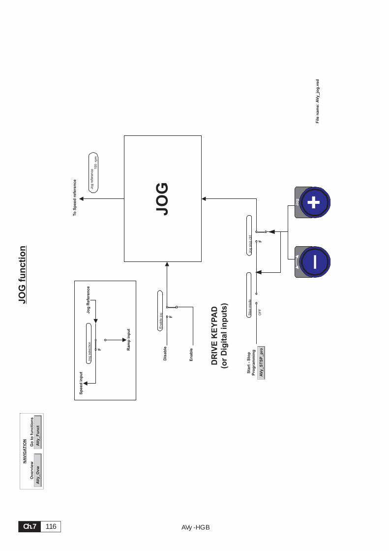
AVy -HGBCh.7 116
JO
Gfu
ncti
on
AV
y_O
vw
Overvie
wNA
VIG
AT
ION
AV
y_F
un
ct
Go
tofu
ncti
on
s
JO
G
DR
IVE
KE
YP
AD
(or
Dig
ita
lin
pu
ts)
Dis
ab
le
En
ab
le
F
F
Sp
ee
din
pu
t
Ram
pin
pu
t
Jo
gR
efe
re
nce
To
Sp
ee
dre
fere
nc
e
FA
Vy_S
TS
P_p
ro
Sta
rt
-S
top
Pro
gram
min
g
+Jo
g
_
En
ab
lejo
g
Jo
gse
lectio
nJo
gre
fere
nce 1
00
rpm
Jo
gsto
pctr
lS
top
mo
de
OF
F
File
nam
e:
AV
y_jo
g.v
sd
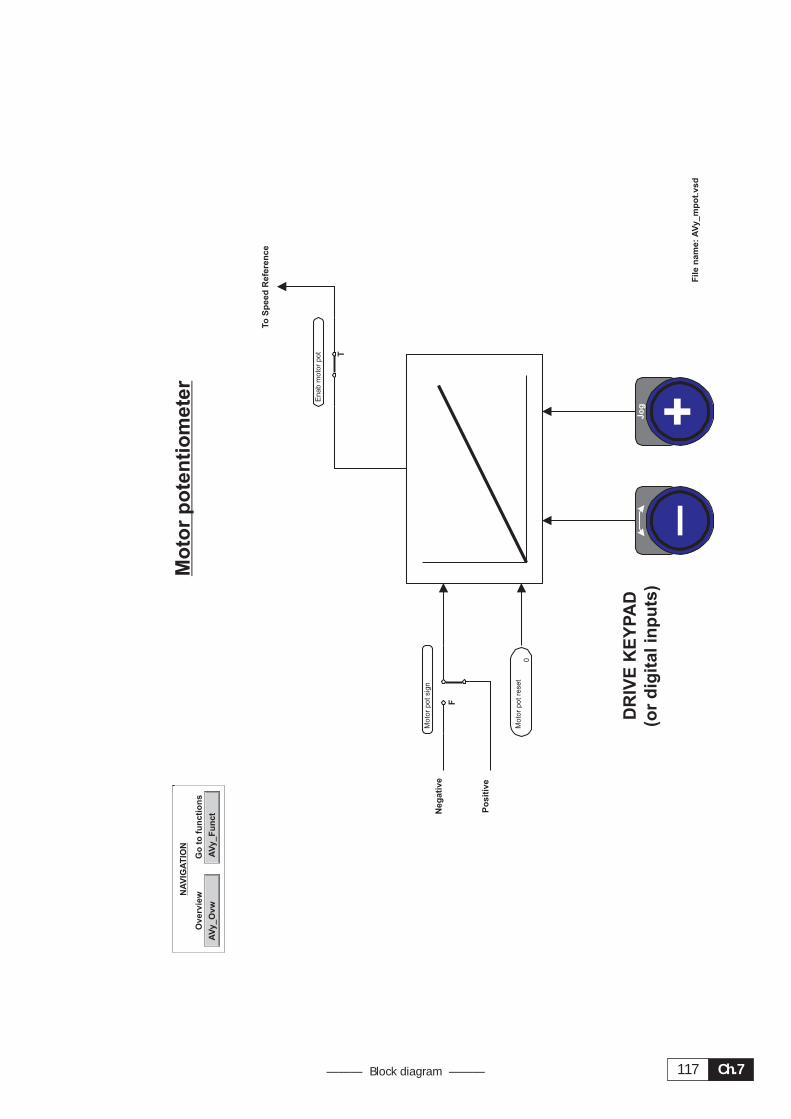
Ch.7117——— Block diagram ———
Mo
tor
po
ten
tio
mete
r
DR
IVE
KE
YP
AD
(or
dig
ita
lin
pu
ts)
Po
sit
ive
Ne
ga
tiv
e
AV
y_
Ov
w
Ov
erv
iewN
AV
IGA
TIO
N
AV
y_
Fu
nc
t
Go
tofu
nc
tio
ns
T
F
To
Sp
ee
dR
efe
re
nc
e
+Jo
g
_
Moto
rpotre
set
0
Enab
moto
rpot
Moto
rpotsig
n
Fil
en
am
e:
AV
y_
mp
ot.
vs
d

AVy -HGBCh.7 118
Mu
lti
sp
ee
dA
Vy
_O
vw
Ov
erv
iewN
AV
IGA
TIO
N
AV
y_
Fu
nc
t
Go
tofu
nc
tio
ns
RE
FE
RE
NC
E
+0 1 0 1 0 1 1
0 0 1 1 0 0 1 1
0 0 0 0 1 1 1 1
Mu
ltisp
ee
dsel
0
Ra
mp
ref
(d)
Sp
ee
dsel0
bit
0n
ot
sele
cte
dS
pe
ed
sel1
bit
1n
ot
sele
cte
dS
pe
ed
sel2
bit
2n
ot
sele
cte
d
Ra
mp
ref
10
rpm
Mu
ltisp
ee
d3
0rp
m
Mu
ltisp
ee
d2
0rp
m
Mu
ltisp
ee
d1
0rp
m
Mu
ltisp
ee
d4
0rp
m
Mu
ltisp
ee
d5
0rp
m
Mu
ltisp
ee
d7
0rp
m
Mu
ltisp
ee
d6
0rp
m
Ra
mp
ref
20
rpm
En
ab
multisp
d Dis
able
d
Fil
en
am
e:
AV
y_
ms
pd
.vs
d
0
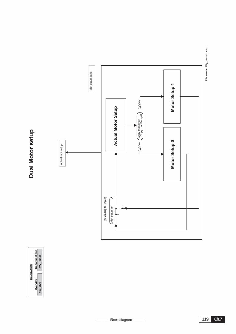
Ch.7119——— Block diagram ———
Du
alM
oto
rsetu
p
AV
y_O
vw
Overvie
wNA
VIG
AT
ION
AV
y_F
un
ct
Go
tofu
ncti
on
s
Mo
tor
Se
tup
0M
oto
rS
etu
p1
Ac
tua
lM
oto
rS
etu
p CO
PY
CO
PY
F
(or
via
Dig
italin
pu
t)
Mo
tse
tup
sta
te
Actu
alm
ot
se
tup
Co
py
mo
tse
tup
Co
py
mo
tS
etu
p0
Mo
tse
tup
se
l
File
nam
e:
AV
y_m
ots
tp.v
sd
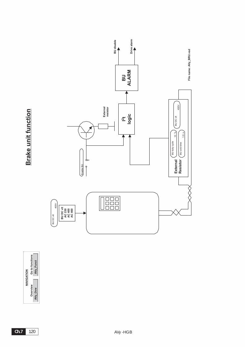
AVy -HGBCh.7 120
Bra
ke
un
itfu
nc
tio
nA
Vy
_O
vw
Ove
rv
iewN
AV
IGA
TIO
N
AV
y_
Fu
nct
Go
tofu
ncti
on
s
BU
DC
vlt
AC
23
0
AC
40
0
AC
46
0
Ex
tern
al
Res
isto
r
I2t
log
ic
BU
AL
AR
M
BU
dis
ab
le
Driv
eala
rm
T
Exte
rn
al
re
sis
tor
BU
DC
vlt
400V
BU
duty
cycle
10
%
BU
ovld
tim
e1.9
s
BU
DC
vlt
400V
Enable
BU
File
na
me:
AV
y_
BR
U.v
sd
Ch.7121——— Block diagram ———
DC
Brakin
gfu
ncti
on
AV
y_O
vw
Ov
ervie
wNA
VIG
AT
ION
AV
y_F
un
ct
Go
tofu
nc
tio
ns
DC
Brakin
gm
od
e
se
lec
tio
n
T
Sp
eed
10
0%
IDC
Ze
ro
sp
dth
re
sh
old
DC
Brakin
gm
od
e0
Sp
eed
10
0%
IDC
Ze
ro
sp
dth
re
sh
old
DC
Brak
ing
mo
de
1
F Ra
mp
sto
p
Qu
ick
sto
p
DC
Brak
ing
cu
rren
t
DC
bra
kin
gm
od
e
DC
bra
kin
gcu
rr5
0%
DC
bra
kin
gd
ela
y5
00
ms
DC
bra
kin
gcu
rr5
0%
Brk
tim
e@
sto
p1
00
0m
s
QS
tpo
pt
co
de
Fil
en
am
e:
AV
y_D
CB
R.v
sd
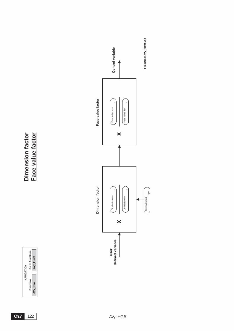
AVy -HGBCh.7 122
Dim
en
sio
nfa
cto
r
Face
valu
efa
cto
r
Dim
en
sio
nfa
cto
r
User
defi
ned
varia
ble
X
AV
y_O
vw
Overvie
wNA
VIG
AT
ION
AV
y_F
un
ct
Go
tofu
ncti
on
s
Face
valu
efa
cto
r
X
Co
ntr
olvaria
ble
Dim
facto
rn
um
1
Dim
facto
rd
en
1
Dim
facto
rte
xt
rpm
Fa
ce
valu
en
um
1
Fa
ce
valu
ed
en
1
File
nam
e:
AV
y_fc
tfct.
vsd
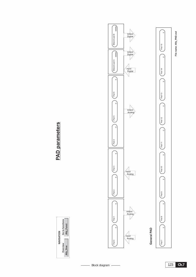
Ch.7123——— Block diagram ———
PA
Dp
aram
ete
rs
Analog
input
Analog
output
Analog
output
Analog
input
Digital
input
Digital
output
Digital
output
Gen
eralP
AD
AV
y_O
vw
Overvie
wNA
VIG
AT
ION
AV
y_F
un
ct
Go
tofu
ncti
on
s
Pa
d0
0P
ad
10
Pa
d2
0P
ad
30
Pa
d4
0P
ad
50
Pa
d6
0B
itw
ord
pa
dA
00
00
hB
itw
ord
pa
dB
00
00
h
Pa
d7
0P
ad
80
Pa
d9
0P
ad
10
0P
ad
11
0P
ad
12
0P
ad
13
0P
ad
14
0P
ad
15
0
File
nam
e:
AV
y_P
AD
.vsd

AVy -HGBCh.7 124
LIN
KS
Fu
ncti
on
+ +X
�+ +
LIN
K1
+ +X
+ +
LIN
K2
AV
y_
Ov
w
Ove
rv
iewN
AV
IGA
TIO
N
AV
y_
Fu
nct
Go
tofu
ncti
on
s
Sourc
e1
0par.
n
Inputabso
lute
1O
ff
Inputoffset1
0
Mulga
in1
1D
ivga
in1
1
Outp
utoffset1
0
Destination
10
par.
n
Inputm
in1
0
Inputm
ax
10
Sourc
e2
0par.
n
Inputabso
lute
2O
ff
Inputoffset2
0
Mulga
in2
1D
ivga
in2
1
Outp
utoffset2
0
Destination
20
pa
r.n
Inputm
in2
0
Inputm
ax
20
�
��
File
na
me:
AV
y_
Lin
ks
.vs
d
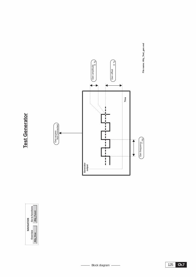
Ch.7125——— Block diagram ———
Te
st
Ge
ne
ra
tor
Ge
ne
ra
tor
ou
tpu
t
Tim
e
AV
y_
Ov
w
Ov
erv
iewN
AV
IGA
TIO
N
AV
y_
Fu
nc
t
Go
tofu
nc
tio
ns
Ge
nfr
eq
ue
ncy 1
Hz
Gen
am
plit
ud
e 0%
Ge
no
ffse
t0
%
Ge
na
cce
ss
No
tC
on
ne
cte
d
Fil
en
am
e:
AV
y_
Te
st_
ge
n.v
sd
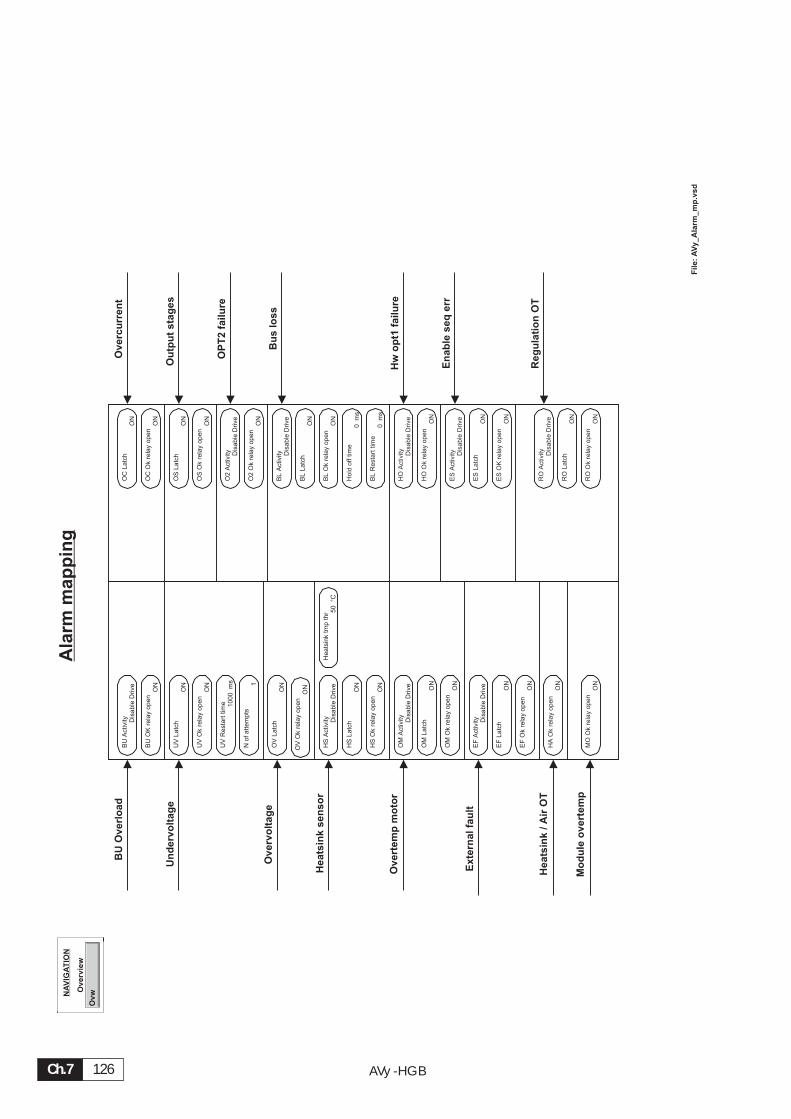
AVy -HGBCh.7 126
Fil
e:
AV
y_A
larm
_m
p.v
sd
Ala
rm
ma
pp
ing
BU
Ov
erlo
ad
Un
de
rv
olt
ag
e
Ov
erv
olt
ag
e
He
ats
ink
se
ns
or
Ov
erte
mp
mo
tor
Ex
tern
al
fau
lt
Ov
erc
urre
nt
Ou
tpu
ts
tag
es
OP
T2
fail
ure
Bu
slo
ss
Hw
op
t1fa
ilu
re
En
ab
les
eq
err
OvwO
vervie
w
NA
VIG
AT
ION
He
ats
ink
/A
irO
T
Mo
du
leo
ve
rte
mp
Re
gu
lati
on
OT
BU
Activity
Dis
able
Drive
BU
OK
rela
yopen
ON
UV
Latc
hO
N
UV
Ok
rela
yopen
ON
UV
Resta
rttim
e 1000
ms
Nofattem
pts
1
OV
Latc
hO
N
OV
Ok
rela
yopen
ON
HS
Activity
Dis
able
Drive
HS
Latc
hO
N
HS
Ok
rela
yopen
ON
ON
OM
Activity
Dis
able
Drive
OM
Latc
hO
N
OM
Ok
rela
yopen
ON
EF
Activity Dis
able
Drive
EF
Latc
hO
N
EF
Ok
rela
yopen
ON
OC
Latc
hO
N
OC
Ok
rela
yopen
ON
OS
Latc
hO
N
OS
Ok
rela
yopen
ON
O2
Activity Dis
able
Drive
O2
Ok
rela
yopen
ON
BL
Activity Dis
able
Drive
BL
Latc
h
BL
Ok
rela
yopen
ON
Hold
off
tim
e0
ms
BL
Resta
rttim
e0
ms
HO
Activity
Dis
able
Drive
HO
Ok
rela
yopen
ON
ES
Activity Dis
able
Drive
ES
Latc
hO
N
ES
OK
rela
yopen
ON
ON
HA
Ok
rela
yopen
ON
MO
Ok
rela
yopen
ON
RO
Activity
Dis
able
Drive
RO
Latc
hO
N
RO
Ok
rela
yopen
Heats
ink
tmp
thr 5
0°C
Ch.8127——— Parameters lists ———
8. PARAMETERS LIST
Explanation of tables:
White text on black background Menu/submenu
White text on black background Menu does not exist in the keypad
in brackets
Fields with gray background Function not accessible via keypad. The status of the correspond-ing parameter is only displayed.
[FF] in the Parameter column Dimension based on the factor function
"No." column Parameter number (decimal). The value 2000H (= decimal8192) must be added to the number given in the “No.” columnin order to obtain the index to access the parameter via Bus ,serial line or Opt2 (APC card). The parameters in the Drivecomgroup can be accessed using the format and index specified inthe DRIVECOM power transmission profile (#21).
"Format" column Internal parameter format:
I= Integer (Example: I16 = Integer 16 bit)
U = Unsigned (Example: U32 = unsigned 32 bit)
Float = Floating point
"Value" column Minimum, maximum and factory parameter values.
S = set value depending on the size of the device.
F = set value depending on the Flt 100 mF [303] parameter
“Factory” column S = factory set value depending on the size of the device.
“Keypad” column √ = Parameter available via keypad
“RS485/BUS/Opt2-M" column Parameter available via RS485, field Bus or via the APC Card
(Low priority) manual communication (see the APC Card user manual)
The numbers indicate what has to be sent via interface line in orderto set the single parameters.
“Term.” column Parameter addressable to one of the analog or digital input/outputterminals.
AVy -HGBCh.8 128
“Opt2-A” (Low Priority)
“PDC” (High Priority) Parameter available via the APC Card asynchronous communica-tion (see the APC Card user manual) and/or the Process DataChannel (PDC) of the Field bus.
NOTE: When field Bus interface parameters whose range is[min=0; max=1] can be assigned to either virtual digital inputs(if “w” access code exists) and/or virtual digital outputs (if “R”access code exists).
IA, QA, ID, QD in the "Term." column The function can be accessed via a freely programmable analog ordigital input or output.
IA = analog input
QA = analog output
ID = digital input
QD = digital output.
The possibly present number is the one by which the terminal isidentified.
H, L in the "Term." column Level of the terminal signals (H=high, L=low) which enables thesingle function.
R/W/Z/C Access possibilities via the serial interface, Bus or Opt2 manual orasynchronous communication :
R = Read, W = Write, Z = Write only when drive disabled,C=Command parameter (the writing of any value causes theexecution of a command).
X · Pyy The value of this parameter can correspond to min/max X timesthe value of the yy parameter.
NOTE ! The parameter number shown in the following table is a base number. The value 2000H(=8192 decimal) must be added to the number given in the “No.” column in order toobtain the index to access the parametr via Bus, serial line or Opt2 (APC card). Theparameters in the Drivecom group can be accessed using the format and index specifiedin the DRIVECOM power transmission profile (#21).
* When the parameter is accessed by Opt2-A/PDC the format is U16** When the parameter is accessed by Opt2-A/PDC the format is I16*** When the parameter is accessed by Opt2-A/PDC the lower word of the parameter is considered
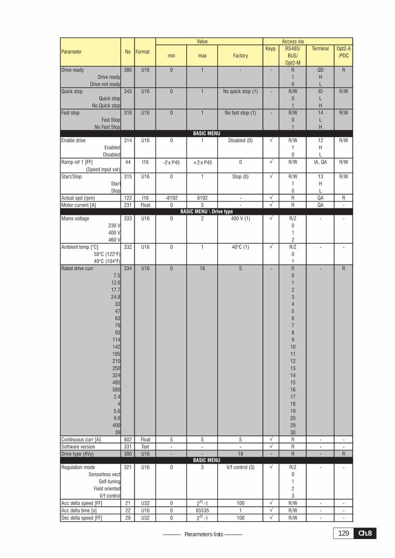
Ch.8129——— Parameters lists ———
Value Access via
Keyp. RS485/ Terminal Opt2-A
min max Factory BUS/ /PDC
Opt2-M
Drive ready 380 U16 0 1 - - R QD R
Drive ready 1 H
Drive not ready 0 L
Quick stop 343 U16 0 1 No quick stop (1) - R/W ID R/W
Quick stop 0 L
No Quick stop 1 H
Fast stop 316 U16 0 1 No fast stop (1) - R/W 14 R/W
Fast Stop 0 L
No Fast Stop 1 H
Enable drive 314 U16 0 1 Disabled (0) � R/W 12 R/W
Enabled 1 H
Disabled 0 L
Ramp ref 1 [FF] 44 I16 -2 x P45 +2 x P45 0 � R/W IA, QA R/W
(Speed input var)
Start/Stop 315 U16 0 1 Stop (0) � R/W 13 R/W
Start 1 H
Stop 0 L
Actual spd (rpm) 122 I16 -8192 8192 - � R QA R
Motor current [A] 231 Float 0 S - � R QA -
Mains voltage 333 U16 0 2 400 V (1) � R/Z - -
230 V 0
400 V 1
460 V 2
Ambient temp [°C] 332 U16 0 1 40°C (1) � R/Z - -
50°C (122°F) 0
40°C (104°F) 1
Rated drive curr 334 U16 0 16 S - R - R
7.5 0
12.6 1
17.7 2
24.8 3
33 4
47 5
63 6
79 7
93 8
114 9
142 10
185 11
210 12
250 13
324 14
485 15
580 16
2.4 17
4 18
5.6 19
9.6 20
400 29
39 30
Continuous curr [A] 802 Float S S S � R - -
Software version 331 Text - - - � R - -
Drive type (AVy) 300 U16 - - 18 - R - R
Regulation mode 321 U16 0 3 V/f control (3) � R/Z - -
Sensorless vect 0
Self-tuning 1
Field oriented 2
V/f control 3
Acc delta speed [FF] 21 U32 0 232 -1 100 � R/W - -
Acc delta time [s] 22 U16 0 65535 1 � R/W - -
Dec delta speed [FF] 29 U32 0 232 -1 100 � R/W - -
BASIC MENU \ Drive type
BASIC MENU
Parameter No Format
BASIC MENU
AVy -HGBCh.8 130
Value Access via
Keyp. RS485/ Terminal Opt2-A
min max Factory BUS/ /PDC
Opt2-M
Dec delta time [s] 30 U16 0 65535 1 R/W - -
T current lim + [%] 8 U16 0 F S R/W IA R/W
T current lim - [%] 9 U16 0 F S R/W IA R/W
Encoder 1 type 415 I16 0 1 Digital (1) R/Z - -
Sinusoidal 0
Digital 1
Encoder 1 pulses 416 Float* 600 9999 1024 R/Z - R
Speed base value [FF] 45 U32*** 1 16383 1500 R/Z - R
Save parameters 256 U16 0 65535 - C - -
Enable drive 314 U16 0 1 Disabled (0) R/W 12 R/W
Enabled 1 H
Disabled 0 L
Start/Stop 315 U16 0 1 Stop (0) R/W 13 R/W
Start 1 H
Stop 0 L
Ramp ref (d) [FF] 109 I16 -32768 32767 - R - R
Ramp output (d) [FF] 112 I16 -32768 32767 - R - R
Speed ref (d) [FF] 115 I16 -32768 32767 - R - R(Speed ref var)
Actual spd (d) [FF] 119 I16 -32768 32767 - R - R(Act spd value)
F act spd (d) [FF] 925 I16 -32768 32767 - R - R
Act spd filter [s] 923 Float 0.001 0.100 0.001 R/W - -
Ramp ref (rpm) 110 I16 -32768 32767 - R QA R
Ramp outp (rpm) 113 I16 -32768 32767 - R QA R
Speed ref (rpm) 118 I16 -32768 32767 - R QA R
Actual spd (rpm) 122 I16 -8192 8192 - R QA R
Enc1 speed [rpm] 427 I16 -8192 8192 - R - R
Enc2 speed [rpm] 420 I16 -8192 8192 - R - R
F act spd (rpm) 924 I16 -32768 32767 - R QA R
Act spd filter [rpm] 923 Float 0.001 0.100 0.001 R/W - -
Ramp ref (%) 111 Float -200.0 + 200.0 - R - -
Ramp output (%) 114 Float -200.0 + 200.0 - R - -
Speed ref (%) 117 Float -200.0 + 200.0 - R - -
Actual spd (%) 121 Float -200.0 + 200.0 - R - -
DC link voltage [V] 227 U16 0 999 - R QA -
Active power [%] 229 Float** -500 500 - R QA R
Output voltage [V] 233 Float** 0 500 - R QA R
Output frequency [Hz] 324 Float 0.0 500.0 - R - -
Motor current [A] 231 Float 0.00 S - R QA -
Torque [%] 230 Float -500 500 - R QA -
T current ref [%] 41 I16 -500 500 - R QA R
T curr (%) 927 I16 -500 500 - R QA R
F T curr (%) 928 I16 -500 500 - R QA R
T curr filter [s] 926 Float 0.001 0.250 0.100 R/W - -
Flux [%] 234 Float* 0.00 100.00 - R QA R
Heatsink temp [°C] 881 I16 - - - R - -
Regulation temp [°C] 1147 I16 - - - R - -
Intake air temp [°C] 914 U16 - - - R QA -
Digital I/Q - - R - -
Dig input term 564 U16 0 65535 - R - R
Dig input term 1 565 U16 0 1 - R - R
Dig input term 2 566 U16 0 1 - R - R
Dig input term 3 567 U16 0 1 - R - R
Dig input term 4 568 U16 0 1 - R - R
Dig input term 5 569 U16 0 1 - R - R
Dig input term 6 570 U16 0 1 - R - R
Dig input term 7 571 U16 0 1 - R - R
MONITOR
MONITOR \ Measurements \ Speed \ Speed in DRC []
Parameter No Format
MONITOR \ Measurements \ Speed \ Speed in rpm
MONITOR \ Measurements \ Speed \ Speed in %
MONITOR \ I/O
MONITOR \ Measurements
Ch.8131——— Parameters lists ———
Value Access via
Keyp. RS485/ Terminal Opt2-A
min max Factory BUS/ /PDC
Opt2-M
Dig input term 8 572 U16 0 1 - - R - R
Dig input term 9 573 U16 0 1 - - R - R
Dig input term 10 574 U16 0 1 - - R - R
Dig input term 11 575 U16 0 1 - - R - R
Dig input term 12 576 U16 0 1 - - R - R
Dig input term 13 577 U16 0 1 - - R - R
Dig input term 14 578 U16 0 1 - - R - R
Dig input term 15 579 U16 0 1 - - R - R
Dig input term 16 580 U16 0 1 - - R - R
Dig output term 581 U16 0 65535 - - R - R
Virtual dig inp 582 U16 0 65535 - R/W - R/W
Virtual dig out 583 U16 0 65535 - R - R
Nominal voltage [V] 161 Float 1 999 400 R/Z - -
Nominal speed [rpm] 162 Float** 1 99999 S R/Z - -
Nom frequency [Hz] 163 Float 1 999 50 R/Z - -
Nominal current [A] 164 Float 0.10 999.00 S R/Z - -
Cos phi 371 Float 0.1 0.99 S R/Z - -
Base voltage [V] 167 Float 1 999 400 R/Z - -
Base frequency [Hz] 168 Float 1 999 50 R/Z - -
Take motor par 694 U16 0 1 - C - -
Magnetizing cur [A] 165 Float 0.10 999.00 S R/W - -
Magn working cur [A] 726 Float 0.10 999.00 S R - -
Rotor resistance [Ohm] 166 Float 0.0001 S S R/W - -
Stator resist [Ohm] 436 Float 0.0001 S S R/W - -
Lkg inductance [H] 437 Float 0.00001 9.00000 S R/W - -
Load motor par 251 U16 0 1 Std400V (0) Z - -
Std for 400V 0
Std for 460V 1
Self tune state 705 U16 0 65535 - R - -
Start part 1 676 U16 0 65535 - C - -
Stator resist [Ohm] 436 Float 0.0001 S S R/W - -
Stator resist Nw [Ohm] 683 Float S S - R - -
Voltage comp lim [V] 644 Float 0.1 30.0 6.0 R/W - -
Volt comp lim Nw [V] 685 Float 0.1 30.0 - R - -
Comp slope [V/A] 645 Float 0.1 50.0 13.0 R/W - -
Comp slope Nw [V/A] 686 Float 0.1 50.0 - R - -
Lkg inductance [H] 437 Float 0.00001 9.00000 S R/W - -
Lkg indutance Nw [H] 684 Float S S - R - -
Current P [%] 89 Float 0.00 100.00 S R/W - -
Current P Nw [%] 687 Float S S - R - -
Rotor resistance [Ohm] 166 Float 0.0001 S S R/W - -
Rotor resist Nw [Ohm] 682 Float S S - R - -
Current I [%] 90 Float 0.00 100.00 S R/W - -
Current I Nw [%] 688 Float S S - R - -
Take val part 1 677 U16 0 65535 - Z/C - -
Start part 2a 678 U16 0 65535 - C - -
P1 flux model 176 Float 0.00 1.00 S R/W - -
P1 flux model Nw 689 Float S S S R - -
P2 flux model 692 U16 1 20 S R/W - -
P2 flux model Nw 690 U16 S S S R - -
Magnetizing curr [A] 165 Float 0.1 999.0 S R/W - -
Magnetiz curr Nw [A] 691 Float S S S R - -
Flux P [%] 91 Float 0.00 100.00 S R/W - -
Flux P Nw [%] 907 Float 0.00 100.00 S R - -
Flux I [%] 92 Float 0.00 100.00 S R/W - -
Flux I Nw [%] 908 Float 0.00 100.00 S R - -
Voltage P [%] 1022 Float 0 100.00 15.00 RW RW -
Voltage P Nw [%] 1024 Float 100.00 0.00 S R R -
DRIVE PARAMETER \ Motor Parameter \ Self-tuning
DRIVE PARAMETER \ Motor Parameter \ Self-tuning \ Self-tune 1
DRIVE PARAMETER \ Mot plate data
DRIVE PARAMETER \ Motor Parameter
DRIVE PARAMETER \ Motor Parameter \ Self-tuning \ Self-tune 2a
Parameter No Format
AVy -HGBCh.8 132
Value Access via
Keyp. RS485/ Terminal Opt2-A
min max Factory BUS/ /PDC
Opt2-M
Voltage I [%] 902 Float 0.00 100.00 4.00 R/W - -
Voltage I Nw [%] 909 Float 0.00 100.00 S R - -
Take val part 2a 679 U16 0 65535 - Z/C - -
Start part 2b 680 U16 0 65535 - C - -
P1 flux model 176 Float 0.00 1.00 S R/W - -
P1 flux model Nw 689 Float S S S R - -
P2 flux model 692 U16 1 20 S R/W - -
P2 flux model Nw 690 U16 S S S R - -
Magnetizing curr [A] 165 Float 0.1 999.0 S R/W - -
Magnetiz curr Nw [A] 691 Float S S S R - -
Flux P [%] 91 Float 0.00 100.00 S R/W - -
Flux P Nw [%] 907 Float 0.00 100.00 S R - -
Flux I [%] 92 Float 0.00 100.00 S R/W - -
Flux I Nw [%] 908 Float 0.00 100.00 S R - -
Voltage P [%] 1022 Float 0.00 100.00 15.00 RW RW -
Voltage P Nw [%] 1024 Float 100.00 0.00 S R R -
Voltage I [%] 902 Float 0.00 100.00 4.00 R/W - -
Voltage I Nw [%] 909 Float 0.00 100.00 S R - -
Take val part 2b 681 U16 0 65535 - Z/C - -
Fwd-Rev spd tune 1029 U16 1 2 Fwd direction (1) R/Z - -
Fwd direction 1
Rev direction 2
Test T curr lim [%] 1048 U16 0 S 20 R/Z - -
Start part 3 1027 U16 0 65535 - C - -
Inertia [kg*m*m*] 1014 Float 0.0010 999.9990 S R/W - -
Inertia Nw [kg*m*m*] 1030 Float 0.0010 999.9990 - R - -
Friction [N*m] 1015 Float 0.000 99.99 S R/W - -
Friction Nw [N*m] 1031 Float 0.000 99.99 - R - -
Speed P [%] 87 Float 0.00 100.00 S R/W - -
Speed P Nw [%] 1032 Float 0.00 100.00 - R - -
Speed I [%] 88 Float 0.00 100.00 S R/W - -
Speed I Nw [%] 1033 Float 0.00 100.00 - R - -
Take val part 3 1028 U16 0 65535 - Z/C - -
Low speed factor 646 I16 0 32000 5000 R/W - -
Sls speed filter [s] 643 Float 0.01 0.50 0.01 R/W - -
Flux corr factor 647 Float 0.50 1.0 0.90 R/W - -
V/f shape 712 U16 0 3 V = k . f 1.0 (0) R/Z - -
V = k . f 1.0 0
V = k . f 1.5 1
V = k . f 1.7 2
V = k . f 2.0 3
Vlt boost type 709 U16 0 1 Manual (0) R/Z - -
Manual 0
Automatic 1
Manual boost [%] 710 Float 0.0 10.0 1.0 R/W - -
Actual boost [%] 711 Float 0.0 100.0 - R - -
Slip comp type 722 U16 0 1 Manual (0) R/Z - -
Manual 0
Automatic 1
Manual slip comp [rpm] 723 I16 0 200 0 R/W - -
Actual slip comp [rpm] 724 I16 -400 400 0 R - -
Slip comp filt [s] 725 Float 0.003 0.300 0.030 R/W - -
Motor losses % 727 Float 0.0 20.0 0 R/W - -
Spd srch time [s] 893 Float 0.01 10.00 10.00 R/W - -
Flux srch time [s] 894 Float 0.01 20.00 1.00 R/W - -
Spd autocapture [FF] 895 I16 -32768 32767 1500 R/W - -
DRIVE PARAMETER \ V/f control
DRIVE PARAMETER \ V/f control \ Voltage boost
DRIVE PARAMETER \ V/f control \ Slip compens
DRIVE PARAMETER \ V/f control \ V/f spd search
DRIVE PARAMETER \ Motor Parameter \ Self-tuning \ Sel-tune 2b
DRIVE PARAMETER \ Motor Parameter \ Self-tuning \ Sel-tune 3
DRIVE PARAMETER \ Sensorless
Parameter No Format
Ch.8133——— Parameters lists ———
Value Access via
Keyp. RS485/ Terminal Opt2-A
min max Factory BUS/ /PDC
Opt2-M
Delay auto cap [ms] 896 U16 0 10000 1000 � R/W - -
Delay retrying [ms] 897 U16 0 10000 1000 � R/W - -
Enable save eng 898 U16 0 1 Disabled (0) � R/Z - -
Enabled 1
Disabled 0
Lock save eng 899 U16 0 1 OFF (0) � R/W ID R/W
OFF 0 L
ON 1 H
V/f flux level [%] 900 U16 0 100 100 � R/W IA R/W
Flux var time [s] 901 U16 1 100 10 � R/W - -
Ramp ref 1 [FF] 44 I16 -2 × P45 +2 × P45 0 � R/W IA, QA R/W
(Speed input var)
Ramp ref 1 (%) 47 Float -200.0 +200.0 0.0 � R/W - -
Ramp ref 2 [FF] 48 I16 -2 × P45 +2 × P45 0 � R/W IA, QA R/W
Ramp ref 2 (%) 49 Float -200.0 +200.0 0.0 � R/W - -
Speed ref 1 [FF] 42 I16 -2 × P45 +2 × P45 0 � R/W IA, QA R/W
Speed ref 1 (%) 378 Float -200.0 +200.0 0.0 � R/W - -
Speed ref 2 [FF] 43 I16 -2 × P45 +2 × P45 0 � R/W IA, QA R/W
Speed Ref 2 (%) 379 Float -200.0 +200.0 0.0 � R/W - -
T current ref 1 [%] 39 I16 F F 0 � R/W IA, QA R/W
T current ref 2 [%] 40 I16 F F 0 � R/W IA, QA R/W
Speed min amount [FF] 1 U32 0 232 -1 0 � R/Z - -
Speed max amount [FF] 2 U32 0 232 -1 5000 � R/Z - -
Speed min pos [FF] 5 U32 0 232 -1 0 � R/Z - -
Speed max pos [FF] 3 U32 0 232 -1 5000 � R/Z - -
Speed min neg [FF] 6 U32 0 232 -1 0 � R/Z - -
Speed max neg [FF] 4 U32 0 232 -1 5000 � R/Z - -
Speed limited 372 U16 0 1 - R QD R
Speed not limited 0 L
Speed limited 1 H
T curr lim type 715 U16 0 1 T lim +/- (0) � R/Z - -
T lim + / - 0
T lim mot gen 1
T lim VDC Ctrl 3
T current lim [%] 7 U16 0 F S � R/W IA R/W
T current lim + [%] 8 U16 0 F S � R/W IA R/W
T current lim - [%] 9 U16 0 F S � R/W IA R/W
Curr limit state 349 U16 0 1 - R QD R
Curr. limit not reached 0 L
Curr. limit reached 1 H
In use Tcur lim+ [%] 10 U16 0 F � R - R
In use Tcur lim- [%] 11 U16 0 F � R - R
Current lim red [%] 13 U16 0 F 100 � R/W - R/W
Torque reduct 342 U16 0 1 Not act. (0) � R/W ID R/W
Not actived 0 L
actived 1 H
Flux level [%] 467 U16 10 100 100 � R/W IA R/W
QA
Dynam vlt margin [%] 889 Float 10.00 10.00 1.00 � R/W - -
Parameter No Format
LIMITS \ Flux limits
LIMITS \ Voltage limits
LIMITS \ Current limits
INPUT VARIABLES \ T current ref
LIMITS \ Speed limits \ Speed amount
LIMITS \ Speed limits \ Speed min/max
INPUT VARIABLES \ Ramp ref \ Ramp ref 1
INPUT VARIABLES \ Ramp ref \ Ramp ref 2
INPUT VARIABLES \ Speed ref \ Speed ref 1
INPUT VARIABLES \ Speed ref \ Speed ref 2
DRIVE PARAMETER \ V/f control \ Energy save
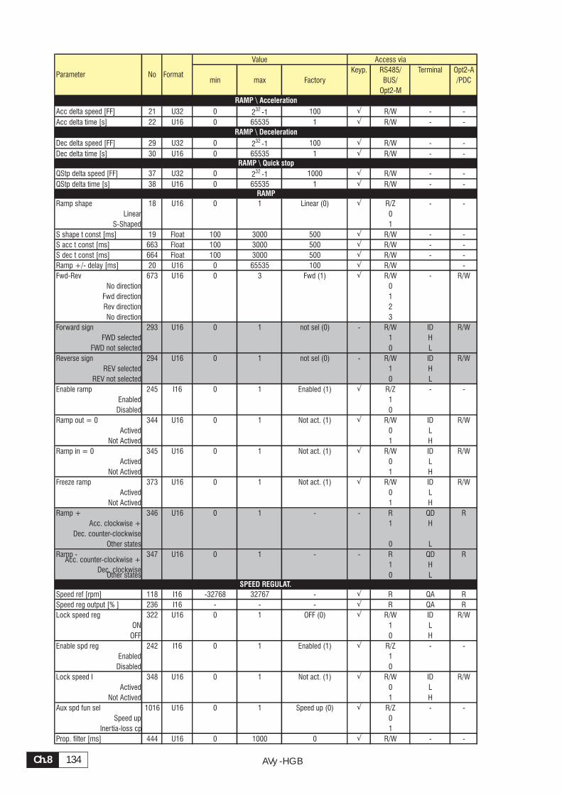
AVy -HGBCh.8 134
Value Access via
Keyp. RS485/ Terminal Opt2-A
min max Factory BUS/ /PDC
Opt2-M
Acc delta speed [FF] 21 U32 0 232 -1 100 � R/W - -
Acc delta time [s] 22 U16 0 65535 1 � R/W - -
Dec delta speed [FF] 29 U32 0 232 -1 100 � R/W - -
Dec delta time [s] 30 U16 0 65535 1 � R/W - -
QStp delta speed [FF] 37 U32 0 232 -1 1000 � R/W - -
QStp delta time [s] 38 U16 0 65535 1 � R/W - -
Ramp shape 18 U16 0 1 Linear (0) � R/Z - -
Linear 0
S-Shaped 1
S shape t const [ms] 19 Float 100 3000 500 � R/W - -
S acc t const [ms] 663 Float 100 3000 500 � R/W - -
S dec t const [ms] 664 Float 100 3000 500 � R/W - -
Ramp +/- delay [ms] 20 U16 0 65535 100 � R/W -
Fwd-Rev 673 U16 0 3 Fwd (1) � R/W - R/W
No direction 0
Fwd direction 1
Rev direction 2
No direction 3
Forward sign 293 U16 0 1 not sel (0) - R/W ID R/W
FWD selected 1 H
FWD not selected 0 L
Reverse sign 294 U16 0 1 not sel (0) - R/W ID R/W
REV selected 1 H
REV not selected 0 L
Enable ramp 245 I16 0 1 Enabled (1) � R/Z - -
Enabled 1
Disabled 0
Ramp out = 0 344 U16 0 1 Not act. (1) � R/W ID R/W
Actived 0 L
Not Actived 1 H
Ramp in = 0 345 U16 0 1 Not act. (1) � R/W ID R/W
Actived 0 L
Not Actived 1 H
Freeze ramp 373 U16 0 1 Not act. (1) � R/W ID R/W
Actived 0 L
Not Actived 1 H
Ramp + 346 U16 0 1 - - R QD R
Acc. clockwise + 1 H
Dec. counter-clockwise
Other states 0 L
Ramp - 347 U16 0 1 - - R QD RAcc. counter-clockwise +
Dec. clockwise1 H
Other states 0 L
Speed ref [rpm] 118 I16 -32768 32767 - � R QA R
Speed reg output [% ] 236 I16 - - - � R QA R
Lock speed reg 322 U16 0 1 OFF (0) � R/W ID R/W
ON 1 L
OFF 0 H
Enable spd reg 242 I16 0 1 Enabled (1) � R/Z - -
Enabled 1
Disabled 0
Lock speed I 348 U16 0 1 Not act. (1) � R/W ID R/W
Actived 0 L
Not Actived 1 H
Aux spd fun sel 1016 U16 0 1 Speed up (0) � R/Z - -
Speed up 0
Inertia-loss cp 1
Prop. filter [ms] 444 U16 0 1000 0 � R/W - -
Parameter No Format
RAMP \ Acceleration
RAMP \ Deceleration
RAMP \ Quick stop
RAMP
SPEED REGULAT.
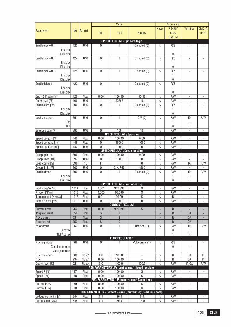
Ch.8135——— Parameters lists ———
Value Access via
Keyp. RS485/ Terminal Opt2-A
min max Factory BUS/ /PDC
Opt2-M
Enable spd=0 I 123 U16 0 1 Disabled (0) R/Z - -
Enabled 1
Disabled 0
Enable spd=0 R 124 U16 0 1 Disabled (0) R/Z - -
Enabled 1
Disabled 0
Enable spd=0 P 125 U16 0 1 Disabled (0) R/Z - -
Enabled 1
Disabled 0
Enable lck sls 422 U16 0 1 Disabled (0) R/Z - -
Enabled 1
Disabled 0
Spd=0 P gain [%] 126 Float 0.00 100.00 10.00 R/W - -
Ref 0 level [FF] 106 U16 1 32767 10 R/W - -
Enable zero pos 890 U16 0 1 Disabled (0) R/Z - -
Enabled 1
Disabled 0
Lock zero pos 891 U16 0 1 OFF (0) R/W ID R/W
ON 1 L
OFF 0 H
Zero pos gain [%] 892 U16 0 100 10 R/W - -
Speed up gain [%] 445 Float 0.00 100.00 0.00 R/W - -
Speed up base [ms] 446 Float 0 16000 1000 R/W - -
Speed up filter [ms] 447 U16 0 1000 0 R/W - -
Droop gain [%] 696 Float 0.00 100.00 0.00 R/W - -
Droop filter [ms] 697 U16 0 1000 0 R/W - -
Load comp [%] 698 I16 F F 0 R/W IA R/W
Droop limit [FF] 700 U16 0 2 × P45 1500 R/W - -
Enable droop 699 U16 0 1 Disabled (0) R/W ID R/W
Enabled 1 H
Disabled 0 L
Inertia [kg*m*m] 1014 Float 0.001 999.999 S R/W - -
Friction [N*m] 1015 Float 0.000 99.999 S R/W - -
Torque const [N*m/A] 1013 Float 0.01 99.99 S R - -
Inertia c filter [ms] 1012 U16 0 1000 0 R/W - -
Current norm 267 Float 0.00 9999.99 S R - -
Torque current 350 Float S S R QA -
Flux current 351 Float S S R QA -
F current ref 352 Float S S R QA -
Zero torque 353 U16 0 1 Not Act. (1) R/W ID R/W
Actived 0 L
Not Actived 1 H
Flux reg mode 469 U16 0 1 Volt.control (1) R/Z -
Constant current 0 -
Voltage control 1
Flux reference 500 Float* 0.0 100.0 - R QA R
Flux 234 Float* 0.00 100.00 - R QA R
Out vlt level [%] 921 Float* 0.0 100.0 100.0 R/W IA,QA R/W
Speed P [%] 87 Float 0.00 100.00 S R/W - -
Speed I [%] 88 Float 0.00 100.00 S R/W - -
Current P [%] 89 Float 0.00 100.00 S R/W - -
Current I [%] 90 Float 0.00 100.00 S R/W - -
Voltage comp lim [V] 644 Float 0.1 30.0 6.0 R/W - -
Comp slope [V/A] 645 Float 0.1 50.0 13.0 R/W - -
SPEED REGULAT \ Spd zero logic
Parameter No Format
REG PARAMETERS \ Percent values \ Current reg\Dead time comp
SPEED REGULAT \ Speed up
SPEED REGULAT \ Droop function
SPEED REGULAT \ Inertia/loss cp
CURRENT REGULAT
FLUX REGULATION
REG PARAMETERS \ Percent values \ Speed regulator
REG PARAMETERS \ Percent values \ Current reg
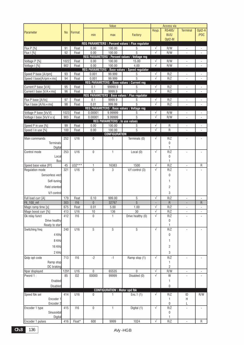
AVy -HGBCh.8 136
Value Access via
Keyp. RS485/ Terminal Opt2-A
min max Factory BUS/ /PDC
Opt2-M
Flux P [%] 91 Float 0.00 100.00 S � R/W - -
Flux I [%] 92 Float 0.00 100.00 S � R/W - -
Voltage P [%] 1022 Float 0.00 100.00 15.00 � R/W - -
Voltage I [%] 902 Float 0.00 100.00 4.00 � R/W - -
Speed P base [A/rpm] 93 Float 0.001 99.999 S � R/Z - -
Speed I base[A/rpm×ms] 94 Float 0.001 99.999 S � R/Z - -
Current P base [V/A] 95 Float 0.1 99999.9 S � R/Z - -
Current I base [V/A×ms] 96 Float 0.1 9999.9 S � R/Z - -
Flux P base [A/Vs] 97 Float 0.1 9999.9 S � R/Z - -
Flux I base [A/Vs×ms] 98 Float 0.01 999.99 S � R/Z - -
Voltage P base [Vs/V] 1023 Float 0.00001 9.99999 S � R/W - -
Voltage I base [Vs/V x s] 903 Float 0.00001 9.99999 S � R/W - -
Speed P in use [%] 99 Float 0.00 100.00 S � R - -
Speed I in use [%] 100 Float 0.00 100.00 S � R - -
Main commands 252 U16 0 1 Terminals (0) � R/Z - -
Terminals 0
Digital 1
Control mode 253 U16 0 1 Local (0) � R/Z - -
Local 0
Bus 1
Speed base value [FF] 45 U32*** 1 16383 1500 � R/Z - R
Regulation mode 321 U16 0 3 V/f control (3) � R/Z - -
Sensorless vect 0
Self-tuning 1
Field oriented 2
V/f control 3
Full load curr [A] 179 Float 0.10 999.00 S � R/Z - -
Flt_100_mf 303 I16 0 32767 S - R - R
Magn ramp time [s] 675 Float 0.01 5.00 1.00 � R/Z - -
Magn boost curr [%] 413 U16 10 136 30 � R/Z - -
Ok relay funct 412 I16 0 1 Drive healthy (0) � R/Z - -
Drive healthy 0
Ready to start 1
Switching freq 240 U16 S S S � R/Z - -
4 KHz 0
8 KHz 1
16 KHz 2
2 KHz 3
Qstp opt code 713 I16 -2 -1 Ramp stop (1) � R/Z - -
Ramp stop 1
DC braking 2
Npar displayed 1291 U16 0 65535 0 � R/W - -
Pword 1 : 85 I32 00000 99999 Disabled (0) � W - -
Enabled 1
Disabled 0
Speed fbk sel 414 U16 0 1 Enc.1 (1) � R/Z ID R/W
Encoder 1 1 H
Encoder 2 0 L
Encoder 1 type 415 I16 0 1 Digital (1) � R/Z - -
Sinusoidal 0
Digital 1
Encoder 1 pulses 416 Float* 600 9999 1024 � R/Z - R
REG PARAMETERS \ Percent values \ Flux regulator
Parameter No Format
REG PARAMETERS \ Base values \ Voltage reg
CONFIGURATION
REG PARAMETERS \ In use values
CONFIGURATION \ Motor spd fbk
REG PARAMETERS \ Percent values \ Voltage reg
REG PARAMETERS \ Base values \ Speed regulator
REG PARAMETERS \ Base values \ Current reg
REG PARAMETERS \ Base values \ Flux regulator
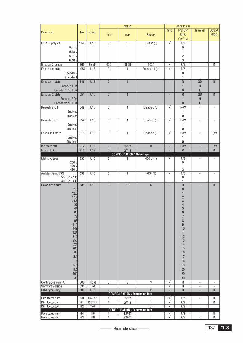
Ch.8137——— Parameters lists ———
Value Access via
Keyp. RS485/ Terminal Opt2-A
min max Factory BUS/ /PDC
Opt2-M
Enc1 supply vlt 1146 U16 0 3 5.41 V (0) � R/Z
5.41 V 0
5.68 V 1
5.91 V 2
6.18 V 3
Encoder 2 pulses 169 Float* 600 9999 1024 � R/Z - R
Encoder repeat 1054 U16 0 1 Encoder 1 (1) � R/Z - -
Encoder 2 0
Encoder 1 1
Encoder 1 state 648 U16 0 1 - - R QD R
Encoder 1 OK 1 H
Encoder 1 NOT OK 0 L
Encoder 2 state 651 U16 0 1 - - R QD R
Encoder 2 OK 1 H
Encoder 2 NOT OK 0 L
Refresh enc 1 649 U16 0 1 Disabled (0) � R/W - -
Enabled 1
Disabled 0
Refresh enc 2 652 U16 0 1 Disabled (0) � R/W - -
Enabled 1
Disabled 0
Enable ind store 911 U16 0 1 Disabled (0) � R/W - R/W
Enabled 1
Disabled 0
Ind store ctrl 912 U16 0 65535 0 - R/W - R/W
Index storing 913 U32 0 232 -1 - - R - R
Mains voltage 333 U16 S 2 400 V (1) � R/Z - -230 V 0400 V 1460 V 2
Ambient temp [°C] 332 U16 0 1 40°C (1) � R/Z - -50°C (122°F) 040°C (104°F) 1
Rated drive curr 334 U16 0 16 S - R - R
7.5 0
12.6 117.7 224.8 3
33 447 563 6
79 7
93 8114 9142 10
185 11210 12250 13324 14485 15
580 16
2.4 17
4 18
5.6 19
9.6 20
400 29
39 30
Continuous curr [A] 802 Float S S S � R - -Software version 331 Text � R - -Drive type (AVy) 300 U16 - - 18 - R - R
Dim factor num 50 I32*** 1 65535 1 � R/Z - R
Dim factor den 51 I32*** 1 232 -1 1 � R/Z - R
Dim factor text 52 Text rpm � R/Z - -
Face value num 54 I16 1 32767 1 � R/Z - RFace value den 53 I16 1 32767 1 � R/Z - R
Parameter No Format
CONFIGURATION \ Face value fact
CONFIGURATION \ Dimension fact
CONFIGURATION \ Drive type
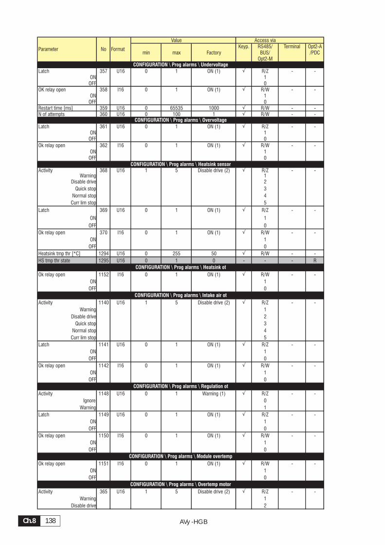
AVy -HGBCh.8 138
Value Access viaKeyp. RS485/ Terminal Opt2-A
min max Factory BUS/ /PDCOpt2-M
Latch 357 U16 0 1 ON (1) � R/Z - -ON 1
OFF 0OK relay open 358 I16 0 1 ON (1) � R/W - -
ON 1OFF 0
Restart time [ms] 359 U16 0 65535 1000 � R/W - -N of attempts 360 U16 0 100 1 � R/W - -
Latch 361 U16 0 1 ON (1) � R/Z - -ON 1
OFF 0
Ok relay open 362 I16 0 1 ON (1) � R/W - -ON 1
OFF 0
Activity 368 U16 1 5 Disable drive (2) � R/Z - -Warning 1
Disable drive 2
Quick stop 3
Normal stop 4
Curr lim stop 5
Latch 369 U16 0 1 ON (1) � R/Z - -
ON 1
OFF 0
Ok relay open 370 I16 0 1 ON (1) � R/W - -
ON 1
OFF 0
Heatsink tmp thr [*C] 1294 U16 0 255 50 � R/W - -
HS tmp thr state 1295 U16 0 1 0 - - - R
Ok relay open 1152 I16 0 1 ON (1) � R/W - -
ON 1
OFF 0
Activity 1140 U16 1 5 Disable drive (2) � R/Z - -
Warning 1
Disable drive 2
Quick stop 3
Normal stop 4
Curr lim stop 5
Latch 1141 U16 0 1 ON (1) � R/Z - -
ON 1
OFF 0
Ok relay open 1142 I16 0 1 ON (1) � R/W - -
ON 1
OFF 0
Activity 1148 U16 0 1 Warning (1) � R/Z - -
Ignore 0
Warning 1
Latch 1149 U16 0 1 ON (1) � R/Z - -
ON 1
OFF 0
Ok relay open 1150 I16 0 1 ON (1) � R/W - -
ON 1
OFF 0
Ok relay open 1151 I16 0 1 ON (1) � R/W - -
ON 1
OFF 0
Activity 365 U16 1 5 Disable drive (2) � R/Z - -
Warning 1
Disable drive 2
Parameter No Format
CONFIGURATION \ Prog alarms \ Overvoltage
CONFIGURATION \ Prog alarms \ Heatsink ot
CONFIGURATION \ Prog alarms \ Regulation ot
CONFIGURATION \ Prog alarms \ Module overtemp
CONFIGURATION \ Prog alarms \ Heatsink sensor
CONFIGURATION \ Prog alarms \ Undervoltage
CONFIGURATION \ Prog alarms \ Intake air ot
CONFIGURATION \ Prog alarms \ Overtemp motor
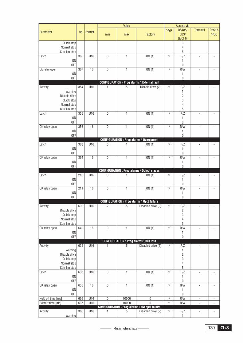
Ch.8139——— Parameters lists ———
Value Access via
Keyp. RS485/ Terminal Opt2-A
min max Factory BUS/ /PDC
Opt2-M
Quick stop 3
Normal stop 4
Curr lim stop 5
Latch 366 U16 0 1 ON (1) � R/Z - -
ON 1
OFF 0
Ok relay open 367 I16 0 1 ON (1) � R/W - -
ON 1
OFF 0
Activity 354 U16 1 5 Disable drive (2) � R/Z - -
Warning 1
Disable drive 2
Quick stop 3
Normal stop 4
Curr lim stop 5
Latch 355 U16 0 1 ON (1) � R/Z - -
ON 1
OFF 0
OK relay open 356 I16 0 1 ON (1) � R/W - -
ON 1
OFF 0
Latch 363 U16 0 1 ON (1) � R/Z - -
ON 1
OFF 0
OK relay open 364 I16 0 1 ON (1) � R/W - -
ON 1
OFF 0
Latch 210 U16 0 1 ON (1) � R/Z - -
ON 1
OFF 0
OK relay open 211 I16 0 1 ON (1) � R/W - -
ON 1
OFF 0
Activity 639 U16 2 5 Disabled drive (2) � R/Z - -
Disable drive 2
Quick stop 3
Normal stop 4
Curr lim stop 5
OK relay open 640 I16 0 1 ON (1) � R/W - -
ON 1
OFF 0
Activity 634 U16 1 5 Disabled drive (2) � R/Z - -
Warning 1
Disable drive 2
Quick stop 3
Normal stop 4
Curr lim stop 5
Latch 633 U16 0 1 ON (1) � R/Z - -
ON 1
OFF 0
OK relay open 635 I16 0 1 ON (1) � R/W - -
ON 1
OFF 0
Hold off time [ms] 636 U16 0 10000 0 � R/W - -
Restart time [ms] 637 U16 0 10000 0 � R/W - -
Activity 386 U16 1 5 Disabled drive (2) � R/Z - -
Warning 1
CONFIGURATION \ Prog alarms \ Output stages
CONFIGURATION \ Prog alarms \ Opt2 failure
CONFIGURATION \ Prog alarms \ Bus loss
CONFIGURATION \ Prog alarms \ Hw opt1 failure
CONFIGURATION \ Prog alarms \ External fault
CONFIGURATION \ Prog alarms \ Overcurrent
Parameter No Format
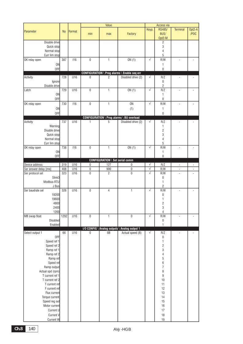
AVy -HGBCh.8 140
Value Access via
Keyp. RS485/ Terminal Opt2-A
min max Factory BUS/ /PDC
Opt2-M
Disable drive 2
Quick stop 3
Normal stop 4
Curr lim stop 5
OK relay open 387 I16 0 1 ON (1) � R/W - -
ON 1
OFF 0
Activity 728 U16 0 2 Disabled drive (2) � R/Z - -
Ignore 0
Disable drive 2
Latch 729 U16 0 1 ON (1) � R/Z - -
ON 1
OFF 0
OK relay open 730 I16 0 1 ON � R/W - -
ON (1) 1
OFF 0
Activity 737 U16 1 5 Disabled drive (2) � R/Z - -
Warning 1
Disable drive 2
Quick stop 3
Normal stop 4
Curr lim stop 5
OK relay open 738 I16 0 1 ON (1) � R/W - -
ON 1
OFF 0
Device address 319 U16 0 127 0 � R/Z - -
Ser answer delay [ms] 408 U16 0 900 0 � R/W - -
Ser protocol sel 323 U16 0 2 0 � R/W - -
Slink3 0
Modbus-RTU 1
J Bus 2
Ser baudrate sel 326 U16 0 4 1 � R/W - -
19200 0
19600 1
4800 2
2400 3
1200 4
MB swap float 1292 U16 0 1 0 � R/W - -
Disabled 0
Enabled 1
Select output 1 66 U16 0 88 Actual speed (8) � R/Z - -
OFF 0
Speed ref 1 1
Speed ref 2 2
Ramp ref 1 3
Ramp ref 2 4
Ramp ref 5
Speed ref 6
Ramp output 7
Actual spd (rpm) 8
T current ref 1 9
T current ref 2 10
T current ref 11
F current ref 12
Flux current 13
Torque current 14
Speed reg out 15
Motor current 16
Current U 17
Current V 18
Current W 19
CONFIGURATION \ Prog alarms \ BU overload
CONFIGURATION \ Prog alarms \ Enable seq err
Parameter No Format
I/O CONFIG \ Analog outputs \ Analog output 1
CONFIGURATION \ Set serial comm
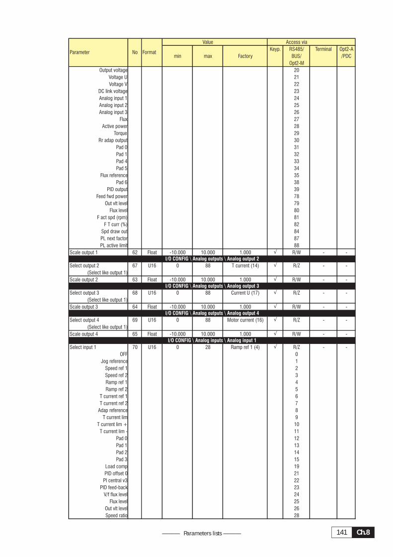
Ch.8141——— Parameters lists ———
Value Access via
Keyp. RS485/ Terminal Opt2-A
min max Factory BUS/ /PDC
Opt2-M
Output voltage 20
Voltage U 21
Voltage V 22
DC link voltage 23
Analog input 1 24
Analog input 2 25
Analog input 3 26
Flux 27
Active power 28
Torque 29
Rr adap output 30
Pad 0 31
Pad 1 32
Pad 4 33
Pad 5 34
Flux reference 35
Pad 6 38
PID output 39
Feed fwd power 78
Out vlt level 79
Flux level 80
F act spd (rpm) 81
F T curr (%) 82
Spd draw out 84
PL next factor 87
PL active limit 88
Scale output 1 62 Float -10.000 10.000 1.000 � R/W - -
Select output 2 67 U16 0 88 T current (14) � R/Z - -
(Select like output 1)
Scale output 2 63 Float -10.000 10.000 1.000 � R/W - -
Select output 3 68 U16 0 88 Current U (17) � R/Z - -
(Select like output 1)
Scale output 3 64 Float -10.000 10.000 1.000 � R/W - -
Select output 4 69 U16 0 88 Motor current (16) � R/Z - -
(Select like output 1)
Scale output 4 65 Float -10.000 10.000 1.000 � R/W - -
Select input 1 70 U16 0 28 Ramp ref 1 (4) � R/Z - -
OFF 0
Jog reference 1
Speed ref 1 2
Speed ref 2 3
Ramp ref 1 4
Ramp ref 2 5
T current ref 1 6
T current ref 2 7
Adap reference 8
T current lim 9
T current lim + 10
T current lim - 11
Pad 0 12
Pad 1 13
Pad 2 14
Pad 3 15
Load comp 19
PID offset 0 21
PI central v3 22
PID feed-back 23
V/f flux level 24
Flux level 25
Out vlt level 26
Speed ratio 28
Parameter No Format
I/O CONFIG \ Analog inputs \ Analog input 1
I/O CONFIG \ Analog outputs \ Analog output 4
I/O CONFIG \ Analog outputs \ Analog output 3
I/O CONFIG \ Analog outputs \ Analog output 2

AVy -HGBCh.8 142
Value Access via
Keyp. RS485/ Terminal Opt2-A
min max Factory BUS/ /PDC
Opt2-M
An in 1 target 295 U16 0 1 Assign. (0) � R/W ID R/W
Assigned 0 L
Not assigned 1 H
Input 1 type 71 U16 0 2 ± 10 V (0) � R/Z - -
-10V ... + 10 V 0
0...20 mA, 0...10 V 1
4...20 mA 2
Input 1 sign 389 U16 0 1 Positive (1) � R/W - R/W
Positive 1
Negative 0
Scale input 1 72 Float -10000 10.000 1.000 � R/W - -
Tune value inp 1 73 Float 0.1 10.000 1.000 � R/W - -
Auto tune inp 1 259 U16 0 65535 - � C - -
Auto tune 1
Input 1 filter [ms] 792 U16 0 1000 0 � R/W - -
Input 1 compare 1042 I16 -10000 10000 0 � R/W - -
Input 1 cp error 1043 U16 0 10000 0 � R/W - -
Input 1 cp delay 1044 U16 0 65000 0 � R/W - -
Input 1 cp match 1045 U16 0 1 - - R QD R
Input 1 not thr.val. 0 L
Input 1=thr.val 1 H
Offset input 1 74 I16 -32768 32767 0 � R/W - -
Select input 2 75 U16 0 28 OFF (0) � R/Z - -
(Select like Input 1)
An in 2 target 296 U16 0 1 Assign.(0) � R/W ID R/W
Assigned 0 L
Not assigned 1 H
Input 2 type 76 U16 0 2 ± 10 V (0) � R/Z - -
-10V ... + 10 V 0
0...20 mA, 0...10 V 1
4...20 mA 2
Input 2 sign 390 U16 0 1 Positive (1) � R/W - R/W
Positive 1
Negative 0
Scale input 2 77 Float -10000 10.000 1.000 � R/W - -
Tune value inp 2 78 Float 0.1 10.000 1.000 � R/W - -
Auto tune inp 2 260 U16 0 65535 - � C - -
Auto tune 1
Offset input 2 79 I16 -32768 32767 0 � R/W - -
Select input 3 80 U16 0 28 OFF (0) � R/Z - -
(Select like Input 1)
An in 3 target 297 U16 0 1 Assign. (0) � R/W ID R/W
Assigned 0 L
Not assigned 1 H
Input 3 type 81 U16 0 2 ± 10 V (0) � R/Z - -
-10V ... + 10 V 0
0...20 mA, 0...10 V 1
4...20 mA 2
Input 3 sign 391 U16 0 1 Positive (1) � R/W - R/W
Positive 1
Negative 0
Scale input 3 82 Float -10000 10.000 1.000 � R/W - -
Tune value inp 3 83 Float 0.1 10.000 1.000 � R/W - -
Auto tune inp 3 261 U16 0 65535 - � C - -
Auto tune 1
Offset input 3 84 I16 -32768 32767 0 � R/W - -
Digital output 1 145 U16 0 63 Ramp + (8) � R/Z - -
OFF 0
Speed zero thr 1
Spd threshold 2
Set speed 3
Curr limit state 4
Parameter No Format
I/O CONFIG \ Analog inputs \ Analog input 3
I/O CONFIG \ Analog inputs \ Analog input 2
I/O CONFIG \ Digital outputs
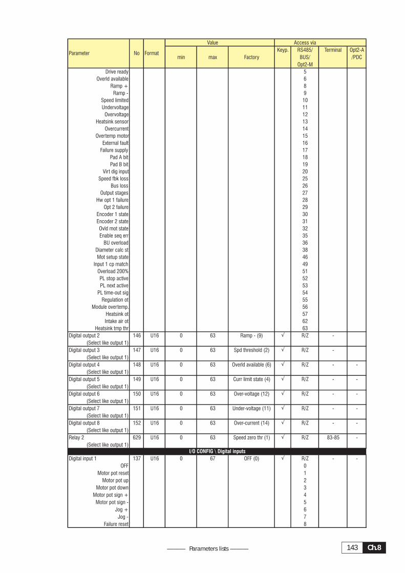
Ch.8143——— Parameters lists ———
Value Access via
Keyp. RS485/ Terminal Opt2-A
min max Factory BUS/ /PDC
Opt2-M
Drive ready 5
Overld available 6
Ramp + 8
Ramp - 9
Speed limited 10
Undervoltage 11
Overvoltage 12
Heatsink sensor 13
Overcurrent 14
Overtemp motor 15
External fault 16
Failure supply 17
Pad A bit 18
Pad B bit 19
Virt dig input 20
Speed fbk loss 25
Bus loss 26
Output stages 27
Hw opt 1 failure 28
Opt 2 failure 29
Encoder 1 state 30
Encoder 2 state 31
Ovld mot state 32
Enable seq err 35
BU overload 36
Diameter calc st 38
Mot setup state 46
Input 1 cp match 49
Overload 200% 51
PL stop active 52
PL next active 53
PL time-out sig 54
Regulation ot 55
Module overtemp. 56
Heatsink ot 57
Intake air ot 62
Heatsink tmp thr 63
Digital output 2 146 U16 0 63 Ramp - (9) � R/Z -
(Select like output 1)
Digital output 3 147 U16 0 63 Spd threshold (2) � R/Z -
(Select like output 1)
Digital output 4 148 U16 0 63 Overld available (6) � R/Z - -
(Select like output 1)
Digital output 5 149 U16 0 63 Curr limit state (4) � R/Z - -
(Select like output 1)
Digital output 6 150 U16 0 63 Over-voltage (12) � R/Z - -
(Select like output 1)
Digital output 7 151 U16 0 63 Under-voltage (11) � R/Z - -
(Select like output 1)
Digital output 8 152 U16 0 63 Over-current (14) � R/Z - -
(Select like output 1)
Relay 2 629 U16 0 63 Speed zero thr (1) � R/Z 83-85 -
(Select like output 1)
Digital input 1 137 U16 0 67 OFF (0) � R/Z - -
OFF 0
Motor pot reset 1
Motor pot up 2
Motor pot down 3
Motor pot sign + 4
Motor pot sign - 5
Jog + 6
Jog - 7
Failure reset 8
Parameter No Format
I/O CONFIG \ Digital inputs
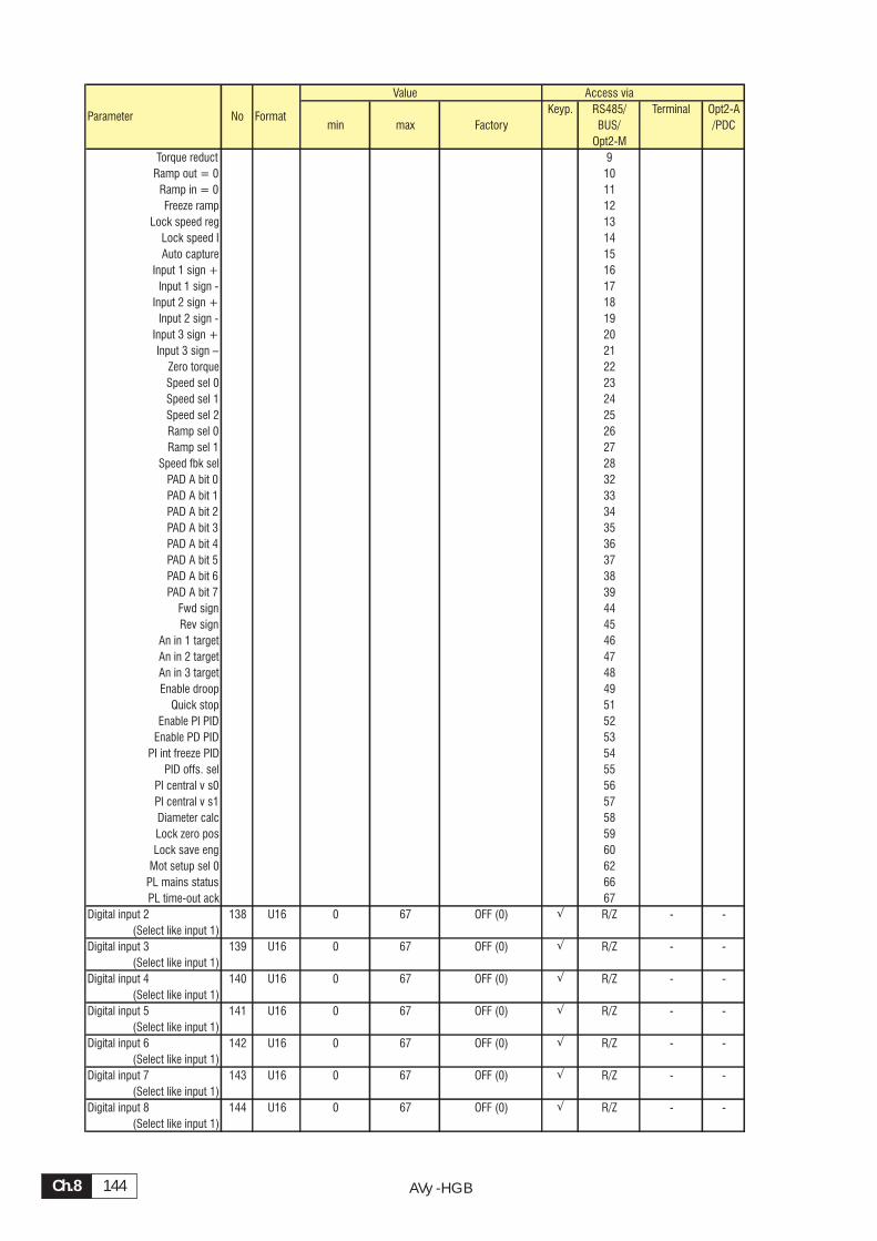
AVy -HGBCh.8 144
Value Access via
Keyp. RS485/ Terminal Opt2-A
min max Factory BUS/ /PDC
Opt2-M
Torque reduct 9
Ramp out = 0 10
Ramp in = 0 11
Freeze ramp 12
Lock speed reg 13
Lock speed I 14
Auto capture 15
Input 1 sign + 16
Input 1 sign - 17
Input 2 sign + 18
Input 2 sign - 19
Input 3 sign + 20
Input 3 sign – 21
Zero torque 22
Speed sel 0 23
Speed sel 1 24
Speed sel 2 25
Ramp sel 0 26
Ramp sel 1 27
Speed fbk sel 28
PAD A bit 0 32
PAD A bit 1 33
PAD A bit 2 34
PAD A bit 3 35
PAD A bit 4 36
PAD A bit 5 37
PAD A bit 6 38
PAD A bit 7 39
Fwd sign 44
Rev sign 45
An in 1 target 46
An in 2 target 47
An in 3 target 48
Enable droop 49
Quick stop 51
Enable PI PID 52
Enable PD PID 53
PI int freeze PID 54
PID offs. sel 55
PI central v s0 56
PI central v s1 57
Diameter calc 58
Lock zero pos 59
Lock save eng 60
Mot setup sel 0 62
PL mains status 66
PL time-out ack 67
Digital input 2 138 U16 0 67 OFF (0) � R/Z - -
(Select like input 1)
Digital input 3 139 U16 0 67 OFF (0) � R/Z - -
(Select like input 1)
Digital input 4 140 U16 0 67 OFF (0) � R/Z - -
(Select like input 1)
Digital input 5 141 U16 0 67 OFF (0) � R/Z - -
(Select like input 1)
Digital input 6 142 U16 0 67 OFF (0) � R/Z - -
(Select like input 1)
Digital input 7 143 U16 0 67 OFF (0) � R/Z - -
(Select like input 1)
Digital input 8 144 U16 0 67 OFF (0) � R/Z - -
(Select like input 1)
Parameter No Format
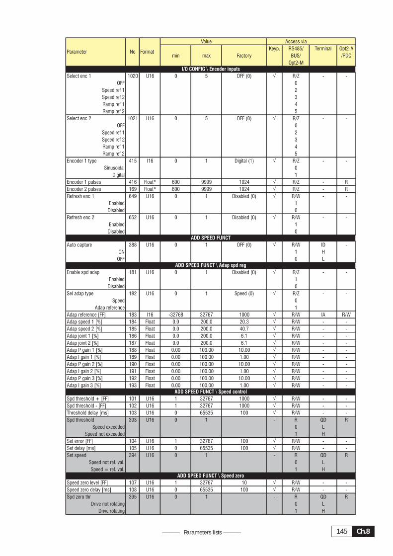
Ch.8145——— Parameters lists ———
Value Access via
Keyp. RS485/ Terminal Opt2-A
min max Factory BUS/ /PDC
Opt2-M
Select enc 1 1020 U16 0 5 OFF (0) � R/Z - -
OFF 0
Speed ref 1 2
Speed ref 2 3
Ramp ref 1 4
Ramp ref 2 5
Select enc 2 1021 U16 0 5 OFF (0) � R/Z - -
OFF 0
Speed ref 1 2
Speed ref 2 3
Ramp ref 1 4
Ramp ref 2 5
Encoder 1 type 415 I16 0 1 Digital (1) � R/Z - -
Sinusoidal 0
Digital 1
Encoder 1 pulses 416 Float* 600 9999 1024 � R/Z - R
Encoder 2 pulses 169 Float* 600 9999 1024 � R/Z - R
Refresh enc 1 649 U16 0 1 Disabled (0) � R/W - -
Enabled 1
Disabled 0
Refresh enc 2 652 U16 0 1 Disabled (0) � R/W - -
Enabled 1
Disabled 0
Auto capture 388 U16 0 1 OFF (0) � R/W ID -
ON 1 H
OFF 0 L
Enable spd adap 181 U16 0 1 Disabled (0) � R/Z - -
Enabled 1
Disabled 0
Sel adap type 182 U16 0 1 Speed (0) � R/Z - -
Speed 0
Adap reference 1
Adap reference [FF] 183 I16 -32768 32767 1000 � R/W IA R/W
Adap speed 1 [%] 184 Float 0.0 200.0 20.3 � R/W - -
Adap speed 2 [%] 185 Float 0.0 200.0 40.7 � R/W - -
Adap joint 1 [%] 186 Float 0.0 200.0 6.1 � R/W - -
Adap joint 2 [%] 187 Float 0.0 200.0 6.1 � R/W - -
Adap P gain 1 [%] 188 Float 0.00 100.00 10.00 � R/W - -
Adap I gain 1 [%] 189 Float 0.00 100.00 1.00 � R/W - -
Adap P gain 2 [%] 190 Float 0.00 100.00 10.00 � R/W - -
Adap I gain 2 [%] 191 Float 0.00 100.00 1.00 � R/W - -
Adap P gain 3 [%] 192 Float 0.00 100.00 10.00 � R/W - -
Adap I gain 3 [%] 193 Float 0.00 100.00 1.00 � R/W - -
Spd threshold + [FF] 101 U16 1 32767 1000 � R/W - -
Spd threshold - [FF] 102 U16 1 32767 1000 � R/W - -
Threshold delay [ms] 103 U16 0 65535 100 � R/W - -
Spd threshold 393 U16 0 1 - R QD R
Speed exceeded 0 L
Speed not exceeded 1 H
Set error [FF] 104 U16 1 32767 100 � R/W - -
Set delay [ms] 105 U16 0 65535 100 � R/W - -
Set speed 394 U16 0 1 - R QD R
Speed not ref. val. 0 L
Speed = ref. val. 1 H
Speed zero level [FF] 107 U16 1 32767 10 � R/W - -
Speed zero delay [ms] 108 U16 0 65535 100 � R/W - -
Spd zero thr 395 U16 0 1 - R QD R
Drive not rotating 0 L
Drive rotating 1 H
Format
ADD SPEED FUNCT \ Speed control
ADD SPEED FUNCT \ Speed zero
ADD SPEED FUNCT
ADD SPEED FUNCT \ Adap spd reg
I/O CONFIG \ Encoder inputs
Parameter No
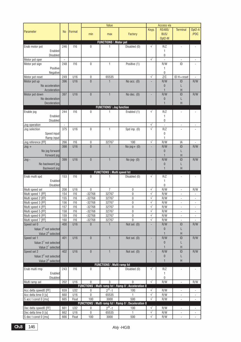
AVy -HGBCh.8 146
Value Access via
Keyp. RS485/ Terminal Opt2-A
min max Factory BUS/ /PDC
Opt2-M
Enab motor pot 246 I16 0 1 Disabled (0) � R/Z - -
Enabled 1
Disabled 0
Motor pot oper - � - - -
Motor pot sign 248 I16 0 1 Positive (1) R/W ID -
Positive 1
Negative 0
Motor pot reset 249 U16 0 65535 � Z/C ID H=reset -
Motor pot up 396 U16 0 1 No acc. (0) - R/W ID R/W
No acceleration 0 L
Acceleration 1 H
Motor pot down 397 U16 0 1 No dec. (0) - R/W ID R/W
No deceleration 0 L
Deceleration 1 H
Enable jog 244 I16 0 1 Enabled (1) � R/Z - -
Enabled 1
Disabled 0
Jog operation - � - - -
Jog selection 375 U16 0 1 Spd inp. (0) � R/Z - -
Speed input 0
Ramp input 1
Jog reference [FF] 266 I16 0 32767 100 � R/W IA -
Jog + 398 U16 0 1 No jog+ (0) - R/W ID R/W
No jog forward 0 L
Forward jog 1 H
Jog - 399 U16 0 1 No jog- (0) - R/W ID R/W
No backward jog 0 L
Backward jog 1 H
Enab multi spd 153 I16 0 1 Disabled (0) � R/Z - -
Enabled 1
Disabled 0
Multi speed sel 208 U16 0 7 0 � R/W - R/W
Multi speed 1 [FF] 154 I16 -32768 32767 0 � R/W - -
Multi speed 2 [FF] 155 I16 -32768 32767 0 � R/W - -
Multi speed 3 [FF] 156 I16 -32768 32767 0 � R/W - -
Multi speed 4 [FF] 157 I16 -32768 32767 0 � R/W - -
Multi speed 5 [FF] 158 I16 -32768 32767 0 � R/W - -
Multi speed 6 [FF] 159 I16 -32768 32767 0 � R/W - -
Multi speed 7 [FF] 160 I16 -32768 32767 0 � R/W - -
Speed sel 0 400 U16 0 1 Not sel. (0) - R/W ID R/W
Value 20 not selected 0 L
Value 20 selected 1 H
Speed sel 1 401 U16 0 1 Not sel. (0) - R/W ID R/W
Value 21 not selected 0 L
Value 21 selected 1 H
Speed sel 2 402 U16 0 1 Not sel. (0) - R/W ID R/W
Value 22 not selected 0 L
Value 22 selected 1 H
Enab multi rmp 243 I16 0 1 Disabled (0) � R/Z - -
Enabled 1
Disabled 0
Multi ramp sel 202 U16 0 3 0 � R/W - R/W
Acc delta speed0 [FF] 659 U32 0 232 -1 100 � R/W - -
Acc delta time 0 [s] 660 U16 0 65535 1 � R/W - -
S acc t const 0 [ms] 665 Float 100 3000 500 � R/W - -
Dec delta speed0 [FF] 661 U32 0 232 -1 100 � R/W - -
Dec delta time 0 [s] 662 U16 0 65535 1 � R/W - -
S dec t const 0 [ms] 666 Float 100 3000 500 � R/W - -
FUNCTIONS \ Multi speed fct
FUNCTIONS \ Motor pot
FUNCTIONS \ Jog function
Parameter No Format
FUNCTIONS \ Multi ramp fct \ Ramp 0 \ Deceleration 0
FUNCTIONS \ Multi ramp fct
FUNCTIONS \ Multi ramp fct \ Ramp 0 \ Acceleration 0
Ch.8147——— Parameters lists ———
Value Access via
Keyp. RS485/ Terminal Opt2-A
min max Factory BUS/ /PDC
Opt2-M
Acc delta speed1 [FF] 23 U32 0 232 -1 100 � R/W - -
Acc delta time 1 [s] 24 U16 0 65535 1 � R/W - -
S acc t const 1 [ms] 667 Float 100 3000 500 � R/W - -
Dec delta speed1 [FF] 31 U32 0 232 -1 100 � R/W - -
Dec delta time 1 [s] 32 U16 0 65535 1 � R/W - -
S dec t const 1 [ms] 668 Float 100 3000 500 � R/W - -
Acc delta speed2 [FF] 25 U32 0 232 -1 100 � R/W - -
Acc delta time 2 [s] 26 U16 0 65535 1 � R/W - -
S acc t const 2 [ms] 669 Float 100 3000 500 � R/W - -
Dec delta speed2 [FF] 33 U32 0 232 -1 100 � R/W - -
Dec delta time 2 [s] 34 U16 0 65535 1 � R/W - -
S dec t const 2 [ms] 670 Float 100 3000 500 � R/W - -
Acc delta speed3 [FF] 27 U32 0 232 -1 100 � R/W - -
Acc delta time 3 [s] 28 U16 0 65535 1 � R/W - -
S acc t const 3 [ms] 671 Float 100 3000 500 � R/W - -
Dec delta speed3 [FF] 35 U32 0 232 -1 100 � R/W - -
Dec delta time 3 [s] 36 U16 0 65535 1 � R/W - -
S dec t const 3 [ms] 672 Float 100 3000 500 � R/W - -
Ramp sel 0 403 U16 0 1 Not sel. (0) - R/W ID R/W
Value 20 not selected 0 L
Value 20 selected 1 H
Ramp sel 1 404 U16 0 1 Not sel. (0) - R/W ID R/W
Value 21 not selected 0 L
Value 21 selected 1 H
Stop mode 626 U16 0 3 1 � R/Z - -
OFF 0
Stop & Speed 0 1
Fast stp & Spd 0 2
Fst / stp & spd 0 3
Spd 0 trip delay [ms] 627 U16 0 40000 0 � R/W - -
Jog stop control 630 U16 0 1 OFF (0) � R/Z - -
ON 1
OFF 0
Speed ratio 1017 I16 0 32767 10000 � R/W IA R/W
Spd draw out (d) 1018 I16 -32767 32767 - � R QA R
Spd draw out (%) 1019 Float -200.0 +200.0 - � R - -
Mot setup sel 943 U16 0 1 Setup 0 (0) � R/Z - R/W
Setup 0 0
Setup 1 1
Mot setup sel 0 940 U16 0 1 Not sel (0) - R/Z ID R/W
Value 2° not sel 0 L
Value 2° sel 1 H
Copy mot setup 941 U16 0 1 Setup 0 (0) � R/Z - -
Setup 0 0
Setup 1 1
Mot setup state 944 U16 0 1 0 - R QD R
Not running 0 L
Running 1 H
Actual mot setup 942 U16 0 1 Setup 0 (0) � R - R
Setup 0 0
Setup 1 1
Motor cont curr [%] 656 U16 50 100 100 � R/W - -
Trip time 50% [s] 657 U16 0 120 60 � R/W - -
FUNCTIONS \ Multi ramp fct \ Ramp 1 \ Acceleration 1
Parameter No Format
FUNCTIONS \ Multi ramp fct \ Ramp 3 \ Acceleration 3
FUNCTIONS \ Multi ramp fct \ Ramp 2 \ Acceleration 2
FUNCTIONS \ Multi ramp fct \ Ramp 1 \ Deceleration 1
FUNCTIONS \ Multi ramp fct \ Ramp 2 \ Deceleration 2
FUNCTIONS \ Motor setup
FUNCTIONS \ Speed draw
FUNCTIONS \ Stop control
FUNCTIONS \ Multi ramp fct \ Ramp 3 \ Deceleration 3
FUNCTIONS \ Overload contr \ Ovld mot contr
AVy -HGBCh.8 148
Value Access via
Keyp. RS485/ Terminal Opt2-A
min max Factory BUS/ /PDC
Opt2-M
Ovld mot state 658 U16 0 1 Not ovrl (1) - R QD R
Overload 0 L
Not overload 1 H
I_sqrt_t_accum [%] 655 U16 0 100 0 � R - R
Ovld Available 406 U16 0 1 - - R QD R
Overload not possible 0 L
Overload possible 1 H
Overload 200% 1139 U16 0 1 - - R QD R
Overload not possible 0 L
Overload possible 1 H
Enable BU 736 U16 0 1 Disabled (0) � R/W - -
Enabled 1
Disabled 0
BU ovld time [s] 740 Float 0.10 50.00 S � R/W
BU duty cycle [%] 741 U16 1 75 S � R/W - -
BU DC vlt [V] 801 U16 0 2 1 � R/W - -
230 0
400 1
460 2
PL stop enable 1083 U16 0 2 0 � R/W - -
Disabled 0
Enabled as Mst 1
Enabled as Slv 2
PL stop t limit [%] 1082 U16 0 F 100 � R/W - -
PL stop acc [rpm/s] 1080 U32 0 99999999 100 � R/W - -
PL stop dec [rpm/s] 1081 U32 0 10000 10000 � R/W - -
PL stop vdc ref [V] 1084 U16 0 800 646 � R/W - -
PL time-out [s] 1087 U16 0 65535 10 � R/W - -
PL stop P Gain [%] 1086 Float 0.00 100.00 5.00 � R/W - -
PL stop I Gain [%] 1085 Float 0.00 100.00 0.30 � R/W - -
PL stop active 1088 U16 0 1 Not active (0) � R - R
Not active 0
Active 1
PL active limit [%] 1089 U16 - - - � R - -
PL next active 1090 U16 0 1 Not active (0) � R - R
Not active 0
Active 1
PL next factor 1091 I16 0 32767 10000 � R - R
PL time-out sig 1093 U16 0 1 Not active (0) � R - R
Not active 0
Active 1
PL time-out ack 1094 U16 0 1 Not acknowledged � R/W - R/W
Not acknowledged (0) 0
Acknowledged 1
PL mains status 1092 U16 0 1 Not ok (0) � R/W - R/W
Not ok 0
Ok 1
VDC Ctrl P Gain [%] 1289 Float 0.00 100 10 � R/W - -
VDC Ctrl I Gain [%] 1290 Float 0.00 100 10 � R/W - -
Gen access 58 U16 0 4 Not conn. (0) � R/Z - -
Not connected 0
F current ref 1
T current ref 2
Flux ref 3
Ramp ref 4
Gen frequency [Hz] 59 Float 0.1 62.5 1.0 � R/W - -
Gen amplitude [%] 60 Float 0.00 200.00 0.00 � R/W - -
Gen offset [%] 61 Float -200.00 200.00 0.00 � R/W - -
Parameter No Format
SPEC FUNCTIONS \ Test generator
FUNCTIONS \ Pwr loss stop f
FUNCTIONS \ Overload contr \ Ovld drv contr
FUNCTIONS \ Brake unit
FUNCTIONS \ VDC control f
Ch.8149——— Parameters lists ———
Value Access via
Keyp. RS485/ Terminal Opt2-A
min max Factory BUS/ /PDC
Opt2-M
Enable rr adap 435 U16 0 1 Disabled (0) � R/W - -
Enabled 1
Disabled 0
Save parameters 256 U16 0 65535 � C - -
Load default 258 U16 0 65535 � Z/C - -
Life time [h.min] 235 Float 0.00 65535.00 � R - -
Failure register - � R - -
Failure text 327 Text - R - -
Failure hour 328 U16 0 65535 - R - -
Failure min 329 U16 0 59 - R - -
Failure code 417 U16 0 65535 - R - -
No failure 0000h
Overcurrent 2300h
Overvoltage 3210h
Undervoltage 3220h
Heatsink sensor 4210h
Heatsink ot 4211h
Regulation ot 4212h
Module overtemp 4213h
Intake air ot 4214h
Overtemp motor 4310h
Failure supply 5100h
Curr fbk loss 5210h
Output stages 5410h
DSP error 6110h
Interrupt error 6120h
BU overload 7110h
Speed fbk loss 7301h
Opt2 7400h
Hw Opt 1failure 7510h
Bus loss 8110h
External fault 9000h
Enable seq err 9009h
Pointer 330 U16 1 10 10 - R/W - -
Failure reset 262 U16 0 65535 � Z/C ID W
H=reset
Failure reg del 263 U16 0 65535 � C - -
DC braking mode 904 U16 0 1 0 � R/Z - -
Enabled 1
Disabled 0
Brk time @ stop [ms] 905 U16 0 30000 1000 � R/W - -
DC braking curr [%] 717 U16 0 100 50 � R/W - -
DC braking delay [ms] 716 U16 0 65535 500 � R/W - -
Source 484 U16 0 65535 0 � R/W - -
Destination 485 U16 0 65535 0 � R/W - -
Mul.Gain 486 Float -10000 10000 1 � R/W - -
Div.Gain 487 Float -10000 10000 1 � R/W - -
Input max 488 Float -231 231 -1 0 � R/W - -
Input min 489 Float -231 231 -1 0 � R/W - -
Input offset 490 Float -231 231 -1 0 � R/W - -
Output offset 491 Float -231 231 -1 0 � R/W - -
Input absolute 492 U16 0 1 OFF (0) � R/W - -
ON 1
OFF 0
Source 553 U16 0 65535 0 � R/W - -
Destination 554 U16 0 65535 0 � R/W - -
Mul.Gain 555 Float -10000 10000 1 � R/W - -
Div.Gain 556 Float -10000 10000 1 � R/W - -
Input max 557 Float -231 231 -1 0 � R/W - -
Input min 558 Float -231 231 -1 0 � R/W - -
SPEC FUNCTIONS \ Links \ Link 2
SPEC FUNCTIONS \ Links \ Link 1
SPEC FUNCTIONS \ DC braking
SPEC FUNCTIONS
Parameter No Format
AVy -HGBCh.8 150
Value Access via
Keyp. RS485/ Terminal Opt2-A
min max Factory BUS/ /PDC
Opt2-M
Input offset 559 Float -231 231 -1 0 � R/W - -
Output offset 560 Float -231 231 -1 0 � R/W - -
Input absolute 561 U16 0 1 OFF (0) � R/W - -
ON 1
OFF 0
Pad 0 503 I16 -32768 32767 0 � R/W IA, QA R/W
Pad 1 504 I16 -32768 32767 0 � R/W IA, QA R/W
Pad 2 505 I16 -32768 32767 0 � R/W IA R/W
Pad 3 506 I16 -32768 32767 0 � R/W IA R/W
Pad 4 507 I16 -32768 32767 0 � R/W QA R/W
Pad 5 508 I16 -32768 32767 0 � R/W QA R/W
Pad 6 509 I16 -32768 32767 0 � R/W QA R/W
Pad 7 510 I16 -32768 32767 0 � R/W - R/W
Pad 8 511 I16 -32768 32767 0 � R/W - R/W
Pad 9 512 I16 -32768 32767 0 � R/W - R/W
Pad 10 513 I16 -32768 32767 0 � R/W - R/W
Pad 11 514 I16 -32768 32767 0 � R/W - R/W
Pad 12 515 I16 -32768 32767 0 � R/W - R/W
Pad 13 516 I16 -32768 32767 0 � R/W - R/W
Pad 14 517 I16 -32768 32767 0 � R/W - R/W
Pad 15 518 I16 -32768 32767 0 � R/W - R/W
Bitword Pad A 519 U16 0 65535 0 � R/W ID*, QD* R/W
Pad A Bit 0 520 U16 0 1 0 - R/W ID, QD R/W
Pad A Bit 1 521 U16 0 1 0 - R/W ID, QD R/W
Pad A Bit 2 522 U16 0 1 0 - R/W ID, QD R/W
Pad A Bit 3 523 U16 0 1 0 - R/W ID, QD R/W
Pad A Bit 4 524 U16 0 1 0 - R/W ID, QD R/W
Pad A Bit 5 525 U16 0 1 0 - R/W ID, QD R/W
Pad A Bit 6 526 U16 0 1 0 - R/W ID, QD R/W
Pad A Bit 7 527 U16 0 1 0 - R/W ID, QD R/W
Pad A Bit 8 528 U16 0 1 0 - R/W QD* -
Pad A Bit 9 529 U16 0 1 0 - R/W QD* -
Pad A Bit 10 530 U16 0 1 0 - R/W QD* -
Pad A Bit 11 531 U16 0 1 0 - R/W QD* -
Pad A Bit 12 532 U16 0 1 0 - R/W QD* -
Pad A Bit 13 533 U16 0 1 0 - R/W QD* -
Pad A Bit 14 534 U16 0 1 0 - R/W QD* -
Pad A Bit 15 535 U16 0 1 0 - R/W QD* -
Bitword Pad B 536 U16 0 65535 0 � R/W QD* R/W
Pad B Bit 0 537 U16 0 1 0 - R/W QD R
Pad B Bit 1 538 U16 0 1 0 - R/W QD R
Pad B Bit 2 539 U16 0 1 0 - R/W QD R
Pad B Bit 3 540 U16 0 1 0 - R/W QD R
Pad B Bit 4 541 U16 0 1 0 - R/W QD R
Pad B Bit 5 542 U16 0 1 0 - R/W QD R
Pad B Bit 6 543 U16 0 1 0 - R/W QD R
Pad B Bit 7 544 U16 0 1 0 - R/W QD R
Pad B Bit 8 545 U16 0 1 0 - R/W QD* -
Pad B Bit 9 546 U16 0 1 0 - R/W QD* -
Pad B Bit 10 547 U16 0 1 0 - R/W QD* -
Pad B Bit 11 548 U16 0 1 0 - R/W QD* -
Pad B Bit 12 549 U16 0 1 0 - R/W QD* -
Pad B Bit 13 550 U16 0 1 0 - R/W QD* -
Pad B Bit 14 551 U16 0 1 0 - R/W QD* -
Pad B Bit 15 552 U16 0 1 0 - R/W QD* -
SBI enable 1293 U16 0 1 0 � R/W - -Disabled 0Enabled 1
Menu
Pdc in 0 1095 U16 0 65535 0 � R/W - -
SPEC FUNCTIONS \ Pad Parameters
Parameter No Format
Accessible only with optional Field bus card
OPTIONS \ Option 1\ PDC config \ PDC inputs
OPTIONS \ Option 1
Ch.8151——— Parameters lists ———
Value Access via
Keyp. RS485/ Terminal Opt2-A
min max Factory BUS/ /PDC
Opt2-M
Pdc in 1 1096 U16 0 65535 0 � R/W - -
Pdc in 2 1097 U16 0 65535 0 � R/W - -
Pdc in 3 1098 U16 0 65535 0 � R/W - -
Pdc in 4 1099 U16 0 65535 0 � R/W - -
Pdc in 5 1100 U16 0 65535 0 � R/W - -
Pdc out 0 1101 U16 0 65535 0 � R/W - -
Pdc out 1 1102 U16 0 65535 0 � R/W - -
Pdc out 2 1103 U16 0 65535 0 � R/W - -
Pdc out 3 1104 U16 0 65535 0 � R/W - -
Pdc out 4 1105 U16 0 65535 0 � R/W - -
Pdc out 5 1106 U16 0 65535 0 � R/W - -
Virt dig in 0 1107 U16 0 65535 0 � R/W - -
Virt dig in 1 1108 U16 0 65535 0 � R/W - -
Virt dig in 2 1109 U16 0 65535 0 � R/W - -
Virt dig in 3 1110 U16 0 65535 0 � R/W - -
Virt dig in 4 1111 U16 0 65535 0 � R/W - -
Virt dig in 5 1112 U16 0 65535 0 � R/W - -
Virt dig in 6 1113 U16 0 65535 0 � R/W - -
Virt dig in 7 1114 U16 0 65535 0 � R/W - -
Virt dig in 8 1115 U16 0 65535 0 � R/W - -
Virt dig in 9 1116 U16 0 65535 0 � R/W - -
Virt dig in 10 1117 U16 0 65535 0 � R/W - -
Virt dig in 11 1118 U16 0 65535 0 � R/W - -
Virt dig in 12 1119 U16 0 65535 0 � R/W - -
Virt dig in 13 1120 U16 0 65535 0 � R/W - -
Virt dig in 14 1121 U16 0 65535 0 � R/W - -
Virt dig in 15 1122 U16 0 65535 0 � R/W - -
Virt dig out 0 1123 U16 0 65535 0 � R/W - -
Virt dig out 1 1124 U16 0 65535 0 � R/W - -
Virt dig out 2 1125 U16 0 65535 0 � R/W - -
Virt dig out 3 1126 U16 0 65535 0 � R/W - -
Virt dig out 4 1127 U16 0 65535 0 � R/W - -
Virt dig out 5 1128 U16 0 65535 0 � R/W - -
Virt dig out 6 1129 U16 0 65535 0 � R/W - -
Virt dig out 7 1130 U16 0 65535 0 � R/W - -
Virt dig out 8 1131 U16 0 65535 0 � R/W - -
Virt dig out 9 1132 U16 0 65535 0 � R/W - -
Virt dig out 10 1133 U16 0 65535 0 � R/W - -
Virt dig out 11 1134 U16 0 65535 0 � R/W - -
Virt dig out 12 1135 U16 0 65535 0 � R/W - -
Virt dig out 13 1136 U16 0 65535 0 � R/W - -
Virt dig out 14 1137 U16 0 65535 0 � R/W - -
Virt dig out 15 1138 U16 0 65535 0 � R/W - -
Menu
Enable OPT2 425 U16 0 1 Disabled (0) � R/Z
Enabled 1
Disabled 0
Enable PI PID 769 U16 0 1 Disabled (0) � R/W ID R/W
Enabled 1
Disabled 0
Enable PD PID 770 U16 0 1 Disabled (0) � R/W ID R/W
Enabled 1
Disabled 0
PID source 786 U16 0 65535 0 � R/W - -
PID source gain 787 Float -100.000 100.000 1.000 � R/W - -
Feed-fwd PID 758 I16 -10000 10000 0 � R IA R
OPTIONS \ PID
OPTIONS \ PID \ PID source
OPTIONS \ PID
Accessible only with optional DGF card (See DGF card user manual)
OPTIONS \ Option 1\ PDC config \ PDC outputs
OPTIONS \ Option 1\ PDC config \ Virt dig in
OPTIONS \ Option 1\ PDC config \ Virt dig out
Parameter No Format
OPTIONS \ Option 2
AVy -HGBCh.8 152
Value Access via
Keyp. RS485/ Terminal Opt2-A
min max Factory BUS/ /PDC
Opt2-M
PID error 759 I16 -10000 10000 0 � R - R
PID feed-back 763 I16 -10000 10000 0 � R/W IA R/W
PID offs. Sel 762 U16 0 1 Offset 0 (0) � R/W ID R/W
Offest 0 0
Offset 1 1
PID offset 0 760 I16 -10000 10000 0 � R/W IA R/W
PID offset 1 761 I16 -10000 10000 0 � R/W - -
PID acc time [s] 1046 Float 0.0 900.0 0.0 � R/W - -
PID dec time [s] 1047 Float 0.0 900.0 0.0 � R/W - -
PID clamp 757 I16 0 10000 10000 � R/W - -
PI P gain PID % 765 Float 0.00 100.00 10.00 � R/W - -
PI I gain PID % 764 Float 0.00 100.00 10.00 � R/W - -
PI steady thr 695 I16 0 10000 0 � R/W - -
PI steady delay [ms] 731 U16 0 60000 0 � R/W - -
P init gain PID % 793 Float 0.00 100.00 10.00 � R/W - -
I init gain PID % 734 Float 0.00 100.00 10.00 � R/W - -
PI central v sel 779 U16 0 3 1 � R/W ID R/W
PI central v1 776 Float P785 P784 1.00 � R/W - -
PI central v2 777 Float P785 P784 1.00 � R/W - -
PI central v3 778 Float P785 P784 1.00 � R/W IA -
PI top lim 784 Float P785 10.00 10.00 � R/W - -
PI bottom lim 785 Float -10.00 P784 0 � R/W - -
PI integr freeze 783 U16 0 1 0 � R/W ID R/W
ON 1
OFF 0
PI output PID 771 I16 0 1000 x 1000 � R - R
P784
Real FF PID 418 I16 -10000 10000 0 � R - R
PD P gain 1 PID [%] 768 Float 0.00 100.00 10.00 � R/W - -
PD D gain 1 PID [%] 766 Float 0.00 100.00 1.00 � R/W - -
PD P gain 2 PID [%] 788 Float 0.00 100.00 10.00 � R/W - -
PD D gain 2 PID [%] 789 Float 0.00 100.00 1.00 � R/W - -
PD P gain 3 PID [%] 790 Float 0.00 100.00 10.00 � R/W - -
PD D gain 3 PID[%] 791 Float 0.00 100.00 1.00 � R/W - -
PD D filter PID [ms] 767 U16 0 1000 0 � R/W - -
PD output PID 421 I16 -10000 10000 0 � R - R
PID out sign PID 772 U16 0 1 1 � R/W - -
Positive 0
Bipolar 1
PID output 774 I16 -10000 10000 0 � R QA R
PID target 782 U16 0 65535 0 � R/W - -
PID out scale 773 Float -100.000 100.000 1.000 � R/W - -
Diameter calc 794 U16 0 1 0 � Z/R ID R/W
Enabled 1
Disabled 0
Positioning spd [rpm] 795 I16 -100 100 0 � R/W - -
Max deviation 796 I16 -10000 10000 8000 � R/W - -
Gear box ratio 797 Float 0.001 1.000 1.000 � R/W - -
Dancer constant [mm] 798 U16 1 10000 1 � R/W - -
Minimum diameter [cm] 799 U16 1 2000 1 � R/W - -
PI central vs0 780 U16 0 1 1 - R/W ID R/W
PI central vs1 781 U16 0 1 0 - R/W ID R/W
Diameter calc st 800 U16 0 1 0 - R QD R
OPTIONS \ PID \ PI controls
OPTIONS \ PID \ PID references
OPTIONS \ PID
OPTIONS \ PID
OPTIONS \ PID \ Diameter calc
OPTIONS \ PID \ PID target
No Format
OPTIONS \ PID
OPTIONS \ PID \ PD controls
Parameter
Ch.8153——— Parameters lists ———
Value Access via
Keyp. RS485/ Terminal Opt2-A
min max Factory BUS/ /PDC
Opt2-M
Malfunction code 57 U16 0 65535 � R - R
No failure 0000hOvercurrent 2300hOvervoltage 3210h
Undervoltage 3220hHeatsink sensor 4210h
Heatsink ot 4211hRegulation ot 4212h
Module overtemp 4213hIntake air ot 4214h
Overtemp motor 4310hFailure supply 5100hCurr fbk loss 5210h
Output stages 5410hDSP error 6110h
Interrupt error 6120hBU overload 7110h
Speed fbk loss 7301hOpt2 7400h
Hw opt 1 failure 7510hBus loss 8110h
External fault 9000hEnable seq err 9009h
Control Word 55 U16 0 65535 0 � R/W - R/W
Status word 56 U16 0 65535 - � R - R
Speed input var [FF] 44 I16 -2 × P45 +2 × P45 0 � R/W IA, QA
(Ramp ref 1)
Speed ref var [FF] 115 I16 -32768 32767 � R - R
(Speed ref)
Act speed value [FF] 119 I16 -32768 32767 � R - R
(Actual spd)
Speed min amount [FF] 1 U32 0 232 -1 0 � R/Z -
Speed max amount [FF] 2 U32 0 232 -1 5000 � R/Z - -
Speed min pos [FF] 5 U32 0 232 -1 0 � R/Z - -
Speed max pos [FF] 3 U32 0 232 -1 5000 � R/Z - -
Speed min neg [FF] 6 U32 0 232 -1 0 � R/Z - -
Speed max neg [FF] 4 U32 0 232 -1 5000 � R/Z - -
Acc delta speed [FF] 21 U32 0 232 -1 100 � R/W - -
Acc delta time [s] 22 U16 0 65535 1 � R/W - -
Dec delta speed [FF] 29 U32 0 232 -1 100 � R/W - -
Dec delta time [s] 30 U16 0 65535 1 � R/W - -
QStp opt code 713 I16 -2 -1 Ramp stop (1) � R/Z -
Ramp stop 1
DC braking curr 2
QStp delta speed [FF] 37 U32 0 232 -1 1000 � R/W - -
QStp delta time [s] 38 U16 0 65535 1 � R/W - -
Face value num 54 I16 1 32767 1 � R/Z - R
Face value den 53 I16 1 32767 1 � R/Z - R
Dim factor num 50 I32*** 1 65535 1 � R/Z - R
Dim factor den 51 I32*** 1 232 -1 1 � R/Z - R
Dim factor text 52 Text rpm � R/Z - -
Speed base value [FF] 45 U32*** 1 16383 1500 � R/Z - R
Speed input perc [%] 46 I16 -32768 32767 0 � R/W - R/W
Percent ref var [%] 116 I16 -32768 32767 0 � R - R
Act percentage [%] 120 I16 -32768 32767 0 � R - R
Password 2 86 � W - -
Parameter No Format
Service
SERVICE
DRIVECOM
DRIVECOM \ Dimension fact
DRIVECOM \ Speed amount
DRIVECOM \ Speed min/max
DRIVECOM \ Acceleration
DRIVECOM \ Quick stop
DRIVECOM \ Face value fact
DRIVECOM \ Deceleration
DRIVECOM
AVy -HGB154
EMC DIRECTIVEThe possible Validity Fields of the EMC Directive (89/336) applied to PDS
“CE marking” summarises the presumption of compliance with the
Essential Requirements of the EMC Directive, which is formulated in the EC Declaration of Conformity
Clauses numbers [.] refer to European Commission document “Guide to the Application of Directive 89/336/EEC”
1997 edition. ISBN 92-828-0762-2
Validity Field
-1-Finished Product/
Complex componentavailable to general public
[Clauses: 3.7, 6.2.1, 6.2.3.1 & 6.3.1]
A PDS (or CDM/BDM) of the Unre-
stricted Distribution class
-2-Finished Product/
Complex componentonly for professional assemblers
[Clauses: 3.7, 6.2.1, 6.2.3.2 & 6.3.2]A PDS (or CDM/BDM)
of the Restricted Distribution class
sold to be included as part of a
system or installation
-3-Installation[Clause: 6.5]
Several combined items of system,
finished product or other components
brought together at a given place. May
include PDSs (CDM or BDM), possibly
of different classes -Restricted or
Unrestricted
-4-System
[Clause: 6.4]
Ready to use finished item(s). May
include PDSs (CDM or BDM), possibly
of different classes
- Restricted or Unrestricted
DescriptionPlaced on the market as a single commercial unit for distribution and final use.
Free movement based on compliance with the EMC Directive
- EC Declaration of conformity required - CE marking required
- PDS or CDM/BDM should comply with IEC 1800-3/EN 61800-3
The manufacturer of the PDS (or CDM/BDM) is responsible for the EMC behaviour of the
PDS (or CDM/BDM), under specified conditions. EMC measures outside the item are described
in an easy to understand fashion and could actually be implemented by a layman in the field of
EMC.
The EMC responsiblity of the assembler of the final product is to follow the manufacturer’s
recommendations and guidelines.
Note: The manufacturer of the PDS (or CDM/BDM) is not responsible for the resulting behaviour
of any system or installation which includes the PDS, see Validity Fields 3 or 4.
Not placed on the marked as a single commercial unit for distribution and final use.
Intended only for professional assemblers who have a level of technical competence to correctly
install.
- No EC Declaration of conformity - No CE marking
- PDS or CDM/BDM should comply with IEC 1800-3/EN 61800-3
The manufacturer of the PDS (or CDM/BDM) is responsible for the provision of installation
guidelines that will assist the manufacturer of the apparatus, system or installation to achieve
compliance.
The resulting EMC behaviour is the responsibility of the manufacturer of the apparatus, system,
or installation, for which its own standards may apply.
Not intended to be placed on the market as a single functional unit (no free movement).
Each system included is subject to the provisions of the EMC Directive.
- No EC Declaration of conformity - No CE marking
- For the PDSs or CDM/BDMs themselves see Validity Fields 1 or 2
- Responsibility of the manufacturer of the PDS may include commissioning
The resulting EMC behaviour is the responsibility of the manufacturer of the installation in co-
operation with the user (e.g. by following an appropriate EMC plan). Essential protection re-
quirements of EMC Directive apply regarding the neighbourhood of the installation.
Has a direct function for the final user. Placed on the market for distribution as a single functional
unit, or as units intended to be easily connected together.
- EC Declaration of conformity required - CE marking required for the system
- For the PDSs or CDM/BDMs themselves see Validity Fields 1 or 2
The resulting EMC behaviour, under specified conditions is the responsibility of the manufac-
turer of the system by using a modular or system approach as appropriate.
Note: The manufacturer of the system is not responsible for the resulting behaviour of any
installation which includes the PDS, see Validity Field 3.
Rel
ates
to
PD
S o
r C
DM
or
BD
M d
irec
tly
Rel
ates
to
app
lica
tion
of
PD
S o
r C
DM
or
BD
M
Examples of application in the different Validity Fields:1 BDM to be used anywhere: (example in domestic premises, or BDM available from commercial distributors), sold without any knowledge of the purchaser or the
application. The manufacture is responsible that sufficient EMC can be achieved even by any unknown customer or layman (snap-in, switch-on).
2 CDM/BDM or PDS for general purpose: to be incorporated in a machine or for industrial application. This is sold as a subassembly to a professional assembler whoincorporates it in a machine, system or installation. Conditions of use are specified in the manufacturer’s documentation. Exchange of technical data allows optimisationof the EMC solution. (See restricted distribution definition).
3 Installation: It can consist of different commercial units (PDS, mechanics, process control etc.). The conditions of incorporation for the PDS (CDM or BDM) arespecified at the time of the order, consequently an exchange of technical data between supplier and client is possible. The combination of the various items in theinstallation should be considered in order to ensure EMC. Harmonic compensation is an evident example of this, for both technical and economical reasons. (E.g.rolling mill, paper machine, crane, etc.)
4 System: Ready to use finished item which includes one or more PDSs (or CDMs/BDMs); e.g. household equipment, air conditioners, standard machine tools,standard pumping systems, etc.


Gef
ran
wo
rld
wid
e
GEFRAN S.p.A.Via Sebina 7425050 Provaglio d’Iseo (BS) ITALYPh. +39 030 98881Fax +39 030 [email protected]
Drive & Motion Control UnitVia Carducci 2421040 Gerenzano [VA] ITALYPh. +39 02 967601Fax +39 02 [email protected]
GEFRAN BENELUXLammerdries-Zuid, 14AB-2250 OLENPh. +32 (0) 14248181Fax. +32 (0) [email protected]
GEFRAN BRASILELETROELETRÔNICAAvenida Dr. Altino Arantes,377/379 Vila Clementino04042-032 SÂO PAULO - SPPh. +55 (0) 1155851133Fax +55 (0) [email protected]
GEFRAN DEUTSCHLANDPhilipp-Reis-Straße 9a63500 SELIGENSTADTPh. +49 (0) 61828090Fax +49 (0) [email protected]
SIEI AREG - GERMANYGottlieb-Daimler-Strasse 17/3D-74385 PleidelsheimPh. +49 7144 89 736 0 Fax +49 7144 89 736 [email protected]
GEFRAN ESpAñA Josep Pla, 163 2°-6ª08020 BARCELONAPh. +34 934982643Fax +34 932662713 [email protected]
GEFRAN - FRANCE4, rue Jean Desparmet - BP 823769355 LYON Cedex 08Ph. +33 (0) 478770300Fax +33 (0) [email protected]
GEFRAN SUISSE SARue Fritz Courvoisier 402302 La Chaux-de-FondsPh. +41 (0) 329684955Fax +41 (0) [email protected]
GEFRAN SIEI - UK Ltd.7 Pearson Road, Central ParkTELFORD, TF2 9TX Ph. +44 (0) 845 2604555Fax +44 (0) 845 [email protected]
GEFRAN INCSensors and Automation8 Lowell AvenueWINCHESTER - MA 01890Toll Free 1-888-888-4474Ph. +1 (781) 7295249Fax +1 (781) [email protected]
Motion Control14201 D South Lakes DriveNC 28273 - CharlottePh. +1 704 3290200Fax +1 704 [email protected]
GEFRAN SIEI - ASIABlk. 30 Loyang way 03-19 Loyang Industrial Estate 508769 SINGAPORE Ph. +65 6 8418300 Fax. +65 6 7428300 [email protected]
GEFRAN SIEI ElectricBlock B, Gr.Flr, No.155, Fu Te Xi Yi Road,Wai Gao Qiao Trade Zone 200131 Shanghai - CHINAPh. +86 21 5866 7816Ph. +86 21 5866 [email protected]
GEFRAN SIEI DRIVES TECHNOLOGYNo.1265, Beihe Road,Jiading District201821 Shanghai - CHINAPh. +86 21 69169898Fax +86 21 [email protected]
GEFRAN INDIA pRIVATE LIMITEDSurvey No.: 129/1, Nandan ParkPlot No.: 6, Chakankar MalaBaner-Balewadi Road, BanerPune 411045, MH, INDIAPh. +91 20 66400400Fax +91 20 66400401
Technical Assistance : [email protected]
Customer Service : [email protected]. +39 02 96760500Fax +39 02 96760278 1S9A30
Manuale AVy QS - ENRev 2.6 - 25.2.2010