Embed Size (px)
Citation preview
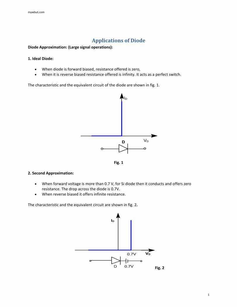
Applications of Diode Diode Approximation: (Large signal operations):
1. Ideal Diode:
• When diode is forward biased, resistance offered is zero, • When it is reverse biased resistance offered is infinity. It acts as a perfect switch.
The characteristic and the equivalent circuit of the diode are shown in fig. 1.
Fig. 1
2. Second Approximation:
• When forward voltage is more than 0.7 V, for Si diode then it conducts and offers zero resistance. The drop across the diode is 0.7V.
• When reverse biased it offers infinite resistance.
The characteristic and the equivalent circuit are shown in fig. 2.
Fig. 2
mywbut.com
1
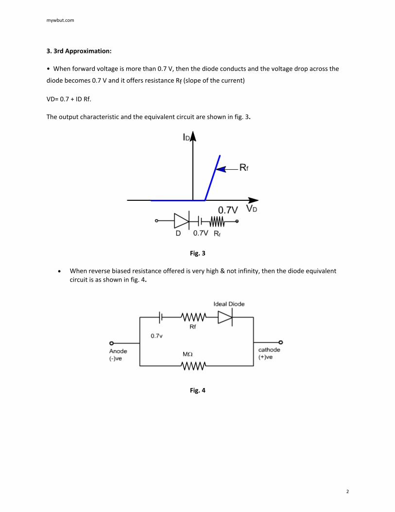
3. 3rd Approximation:
• When forward voltage is more than 0.7 V, then the diode conducts and the voltage drop across the
diode becomes 0.7 V and it offers resistance Rf (slope of the current)
VD= 0.7 + ID Rf.
The output characteristic and the equivalent circuit are shown in fig. 3.
Fig. 3
• When reverse biased resistance offered is very high & not infinity, then the diode equivalent circuit is as shown in fig. 4.
Fig. 4
mywbut.com
2
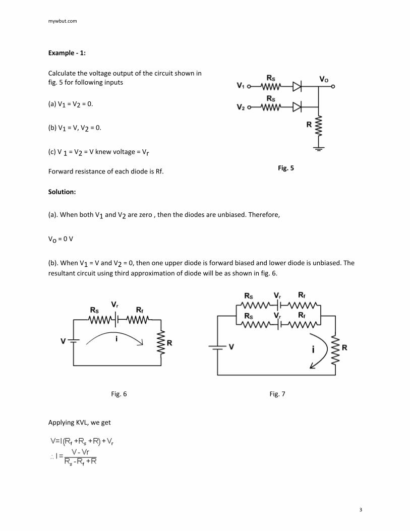
Example - 1:
Calculate the voltage output of the circuit shown in fig. 5 for following inputs
(a) V1 = V2 = 0.
(b) V1 = V, V2 = 0.
(c) V 1 = V2 = V knew voltage = Vr
Forward resistance of each diode is Rf.
Fig. 5
Solution:
(a). When both V1 and V2 are zero , then the diodes are unbiased. Therefore,
Vo = 0 V
(b). When V1 = V and V2 = 0, then one upper diode is forward biased and lower diode is unbiased. The resultant circuit using third approximation of diode will be as shown in fig. 6.
Fig. 6 Fig. 7
Applying KVL, we get
mywbut.com
3
(c) When both V1 and V2 are same as V, then both the diodes are forward biased and conduct. The resultant circuit using third approximation of diode will be as shown in Fig. 7.
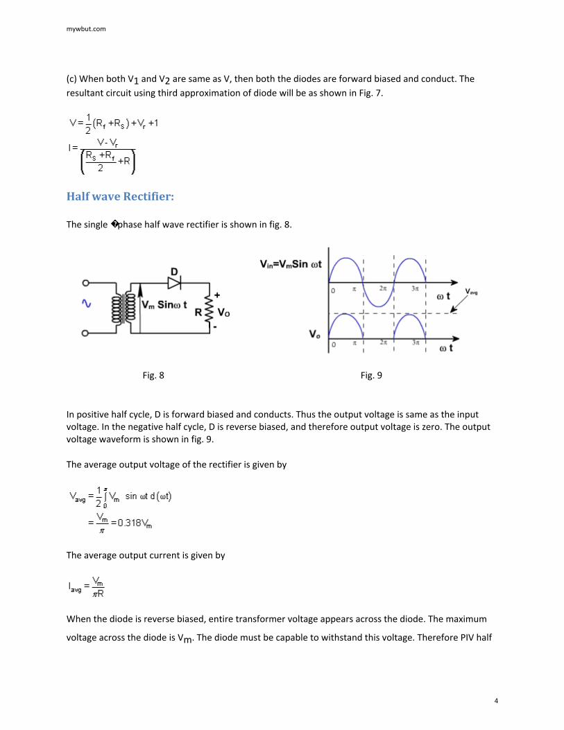
Half wave Rectifier:
The single � phase half wave rectifier is shown in fig. 8.
Fig. 8 Fig. 9
In positive half cycle, D is forward biased and conducts. Thus the output voltage is same as the input voltage. In the negative half cycle, D is reverse biased, and therefore output voltage is zero. The output voltage waveform is shown in fig. 9.
The average output voltage of the rectifier is given by
The average output current is given by
When the diode is reverse biased, entire transformer voltage appears across the diode. The maximum
voltage across the diode is Vm. The diode must be capable to withstand this voltage. Therefore PIV half
mywbut.com
4
wave rating of diode should be equal to Vm in case of single-phase rectifiers. The average current rating
must be greater than Iavg
Full Wave Rectifier:
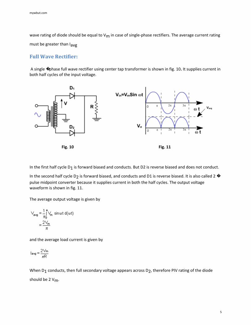
A single � phase full wave rectifier using center tap transformer is shown in fig. 10. It supplies current in both half cycles of the input voltage.
Fig. 10 Fig. 11
In the first half cycle D1 is forward biased and conducts. But D2 is reverse biased and does not conduct.
In the second half cycle D2 is forward biased, and conducts and D1 is reverse biased. It is also called 2 � pulse midpoint converter because it supplies current in both the half cycles. The output voltage waveform is shown in fig. 11.
The average output voltage is given by
and the average load current is given by
When D1 conducts, then full secondary voltage appears across D2, therefore PIV rating of the diode
should be 2 Vm.
mywbut.com
5
Clipper Circuits
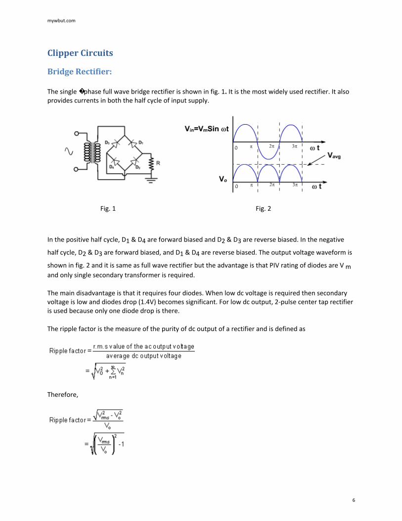
Bridge Rectifier:
The single � phase full wave bridge rectifier is shown in fig. 1. It is the most widely used rectifier. It also provides currents in both the half cycle of input supply.
Fig. 1 Fig. 2
In the positive half cycle, D1 & D4 are forward biased and D2 & D3 are reverse biased. In the negative
half cycle, D2 & D3 are forward biased, and D1 & D4 are reverse biased. The output voltage waveform is
shown in fig. 2 and it is same as full wave rectifier but the advantage is that PIV rating of diodes are V m and only single secondary transformer is required.
The main disadvantage is that it requires four diodes. When low dc voltage is required then secondary voltage is low and diodes drop (1.4V) becomes significant. For low dc output, 2-pulse center tap rectifier is used because only one diode drop is there.
The ripple factor is the measure of the purity of dc output of a rectifier and is defined as
Therefore,
mywbut.com
6
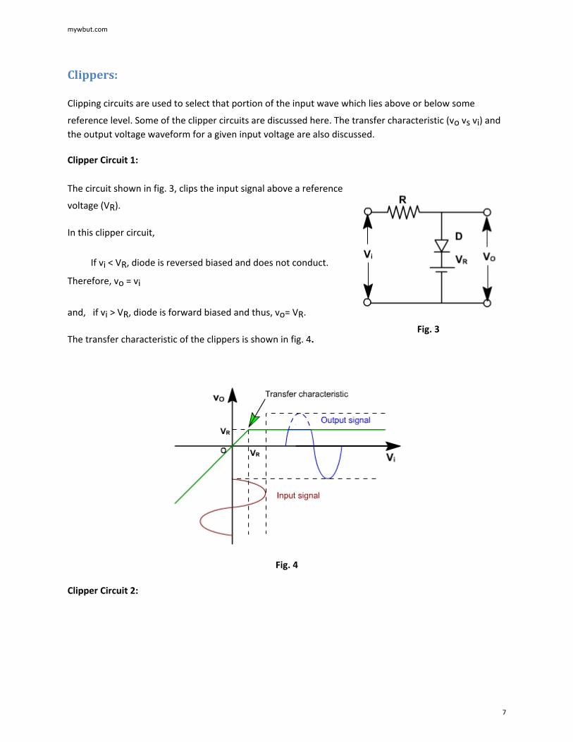
Clippers:
Clipping circuits are used to select that portion of the input wave which lies above or below some
reference level. Some of the clipper circuits are discussed here. The transfer characteristic (vo vs vi) and the output voltage waveform for a given input voltage are also discussed.
Clipper Circuit 1:
The circuit shown in fig. 3, clips the input signal above a reference
voltage (VR).
In this clipper circuit,
If vi < VR, diode is reversed biased and does not conduct.
Therefore, vo = vi
and, if vi > VR, diode is forward biased and thus, vo= VR.
The transfer characteristic of the clippers is shown in fig. 4.
Fig. 3
Fig. 4
Clipper Circuit 2:
mywbut.com
7
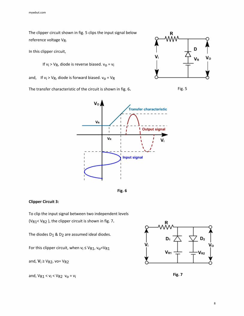
The clipper circuit shown in fig. 5 clips the input signal below
reference voltage VR.
In this clipper circuit,
If vi > VR, diode is reverse biased. vo = vi
and, If vi > VR, diode is forward biased. vo = VR
The transfer characteristic of the circuit is shown in fig. 6.
Fig. 5
Fig. 6
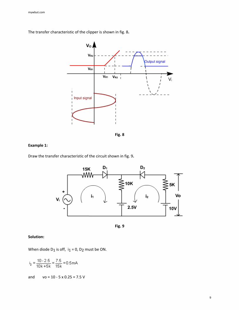
Clipper Circuit 3:
To clip the input signal between two independent levels
(VR1< VR2 ), the clipper circuit is shown in fig. 7.
The diodes D1 & D2 are assumed ideal diodes.
For this clipper circuit, when vi ≤ VR1, vo=VR1
and, vi ≥ VR2, vo= VR2
and, VR1 < vi < VR2 vo = vi
Fig. 7
mywbut.com
8
The transfer characteristic of the clipper is shown in fig. 8.
Fig. 8
Example 1:
Draw the transfer characteristic of the circuit shown in fig. 9.
Fig. 9
Solution:
When diode D1 is off, i1 = 0, D2 must be ON.
and vo = 10 - 5 x 0.25 = 7.5 V
mywbut.com
9
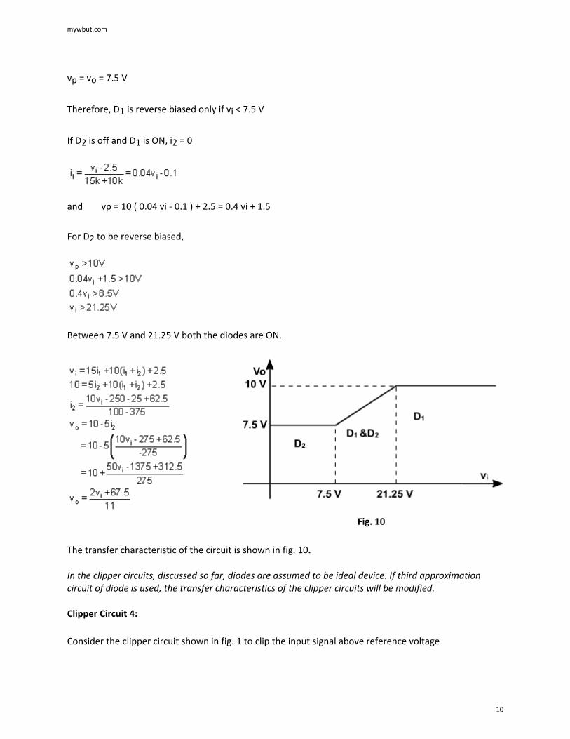
vp = vo = 7.5 V
Therefore, D1 is reverse biased only if vi < 7.5 V
If D2 is off and D1 is ON, i2 = 0
and vp = 10 ( 0.04 vi - 0.1 ) + 2.5 = 0.4 vi + 1.5
For D2 to be reverse biased,
Between 7.5 V and 21.25 V both the diodes are ON.
Fig. 10
The transfer characteristic of the circuit is shown in fig. 10.
In the clipper circuits, discussed so far, diodes are assumed to be ideal device. If third approximation circuit of diode is used, the transfer characteristics of the clipper circuits will be modified.
Clipper Circuit 4:
Consider the clipper circuit shown in fig. 1 to clip the input signal above reference voltage
mywbut.com
10
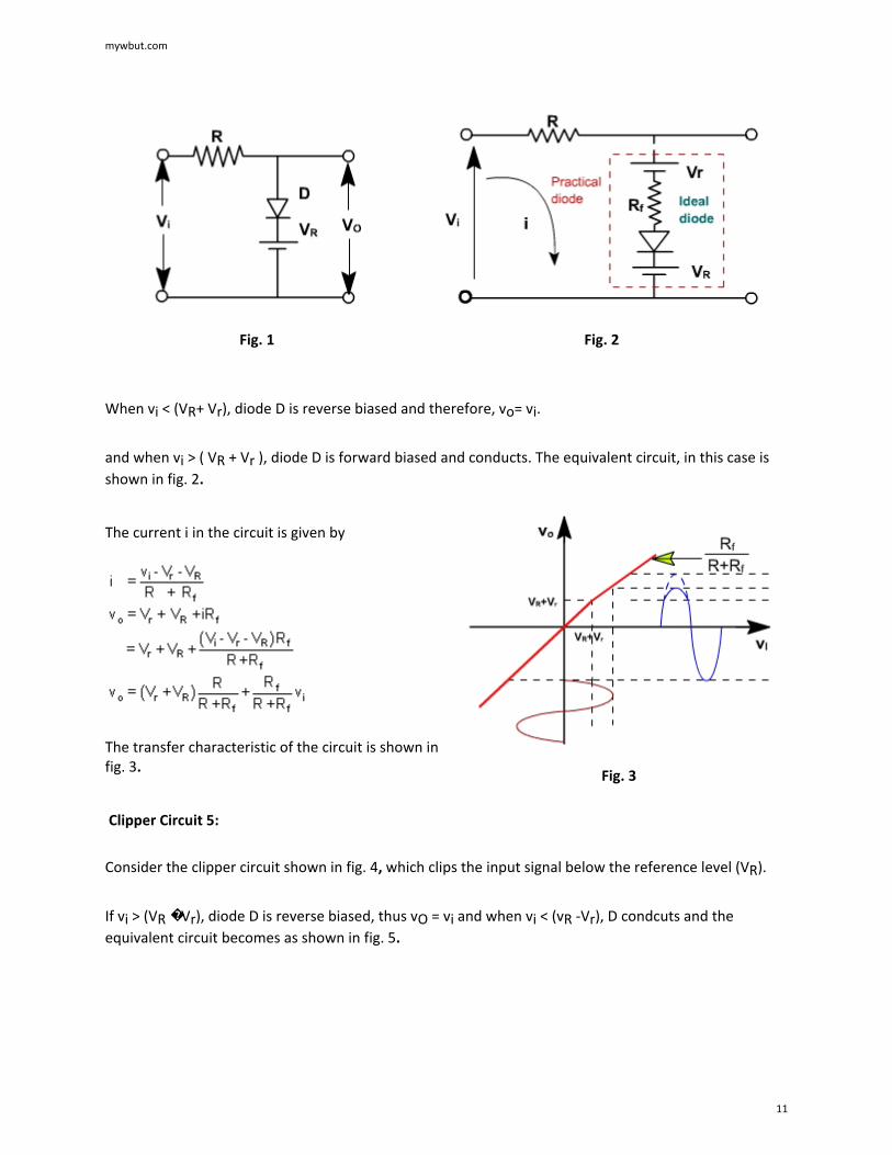
Fig. 1 Fig. 2
When vi < (VR+ Vr), diode D is reverse biased and therefore, vo= vi.
and when vi > ( VR + Vr ), diode D is forward biased and conducts. The equivalent circuit, in this case is shown in fig. 2.
The current i in the circuit is given by
The transfer characteristic of the circuit is shown in fig. 3.
Fig. 3
Clipper Circuit 5:
Consider the clipper circuit shown in fig. 4, which clips the input signal below the reference level (VR).
If vi > (VR � Vr), diode D is reverse biased, thus vO = vi and when vi < (vR -Vr), D condcuts and the equivalent circuit becomes as shown in fig. 5.
mywbut.com
11
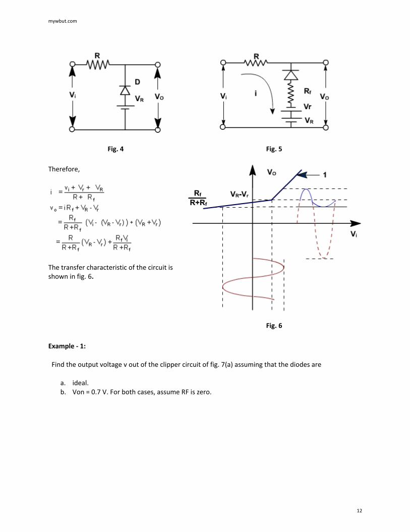
Fig. 4 Fig. 5
Therefore,
The transfer characteristic of the circuit is shown in fig. 6.
Fig. 6
Example - 1:
Find the output voltage v out of the clipper circuit of fig. 7(a) assuming that the diodes are
a. ideal. b. Von = 0.7 V. For both cases, assume RF is zero.
mywbut.com
12
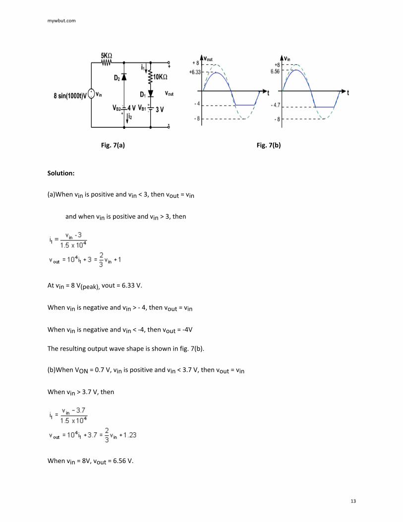
Fig. 7(a) Fig. 7(b)
Solution:
(a)When vin is positive and vin < 3, then vout = vin
and when vin is positive and vin > 3, then
At vin = 8 V(peak), vout = 6.33 V.
When vin is negative and vin > - 4, then vout = vin
When vin is negative and vin < -4, then vout = -4V
The resulting output wave shape is shown in fig. 7(b).
(b)When VON = 0.7 V, vin is positive and vin < 3.7 V, then vout = vin
When vin > 3.7 V, then
When vin = 8V, vout = 6.56 V.
mywbut.com
13
When vin is negative and vin > -4.7 V, then vout = vin
When vin < - 4.7 V, then vout = - 4.7 V
The resulting output wave form is shown in fig. 7(b).
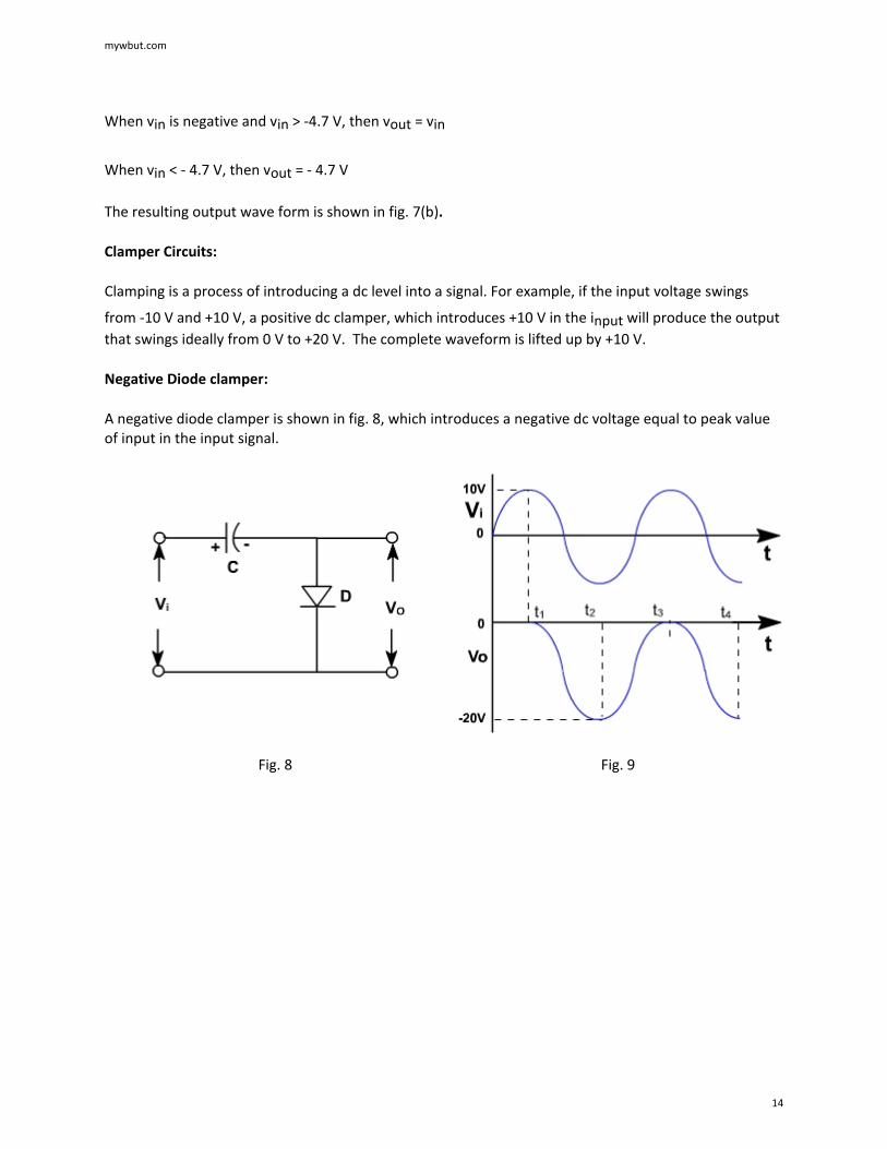
Clamper Circuits:
Clamping is a process of introducing a dc level into a signal. For example, if the input voltage swings
from -10 V and +10 V, a positive dc clamper, which introduces +10 V in the input will produce the output that swings ideally from 0 V to +20 V. The complete waveform is lifted up by +10 V.
Negative Diode clamper:
A negative diode clamper is shown in fig. 8, which introduces a negative dc voltage equal to peak value of input in the input signal.
Fig. 8 Fig. 9
mywbut.com
14
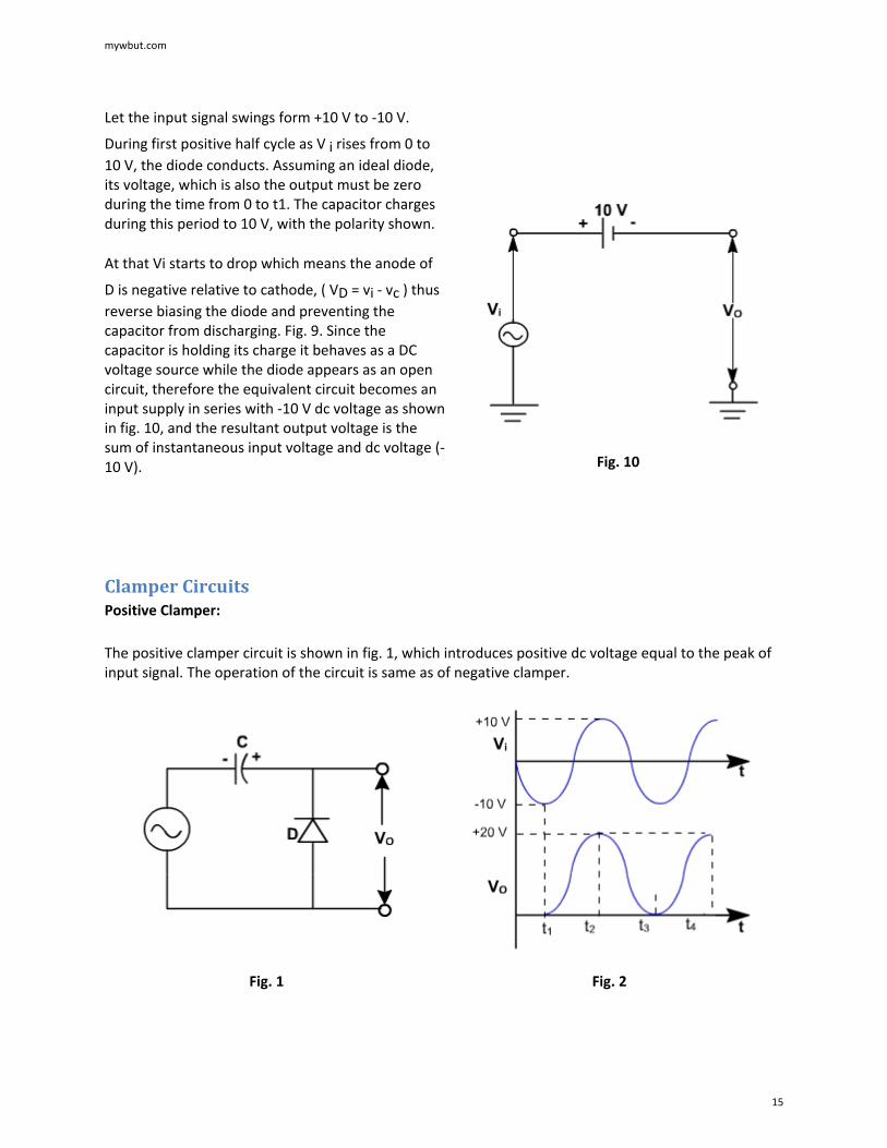
Let the input signal swings form +10 V to -10 V.
During first positive half cycle as V i rises from 0 to 10 V, the diode conducts. Assuming an ideal diode, its voltage, which is also the output must be zero during the time from 0 to t1. The capacitor charges during this period to 10 V, with the polarity shown.
At that Vi starts to drop which means the anode of
D is negative relative to cathode, ( VD = vi - vc ) thus reverse biasing the diode and preventing the capacitor from discharging. Fig. 9. Since the capacitor is holding its charge it behaves as a DC voltage source while the diode appears as an open circuit, therefore the equivalent circuit becomes an input supply in series with -10 V dc voltage as shown in fig. 10, and the resultant output voltage is the sum of instantaneous input voltage and dc voltage (-10 V).
Fig. 10
Clamper Circuits Positive Clamper:
The positive clamper circuit is shown in fig. 1, which introduces positive dc voltage equal to the peak of input signal. The operation of the circuit is same as of negative clamper.
Fig. 1 Fig. 2
mywbut.com
15
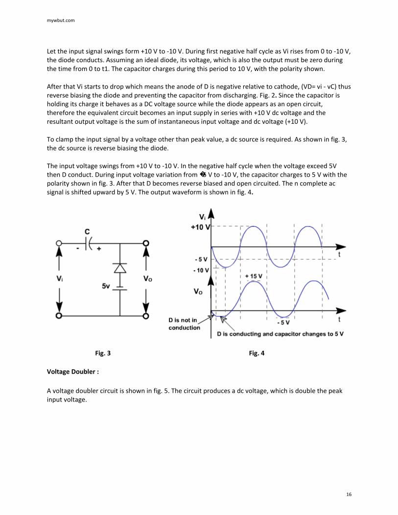
Let the input signal swings form +10 V to -10 V. During first negative half cycle as Vi rises from 0 to -10 V, the diode conducts. Assuming an ideal diode, its voltage, which is also the output must be zero during the time from 0 to t1. The capacitor charges during this period to 10 V, with the polarity shown.
After that Vi starts to drop which means the anode of D is negative relative to cathode, (VD= vi - vC) thus reverse biasing the diode and preventing the capacitor from discharging. Fig. 2. Since the capacitor is holding its charge it behaves as a DC voltage source while the diode appears as an open circuit, therefore the equivalent circuit becomes an input supply in series with +10 V dc voltage and the resultant output voltage is the sum of instantaneous input voltage and dc voltage (+10 V).
To clamp the input signal by a voltage other than peak value, a dc source is required. As shown in fig. 3, the dc source is reverse biasing the diode.
The input voltage swings from +10 V to -10 V. In the negative half cycle when the voltage exceed 5V then D conduct. During input voltage variation from �5 V to -10 V, the capacitor charges to 5 V with the polarity shown in fig. 3. After that D becomes reverse biased and open circuited. The n complete ac signal is shifted upward by 5 V. The output waveform is shown in fig. 4.
Fig. 3 Fig. 4
Voltage Doubler :
A voltage doubler circuit is shown in fig. 5. The circuit produces a dc voltage, which is double the peak input voltage.
mywbut.com
16
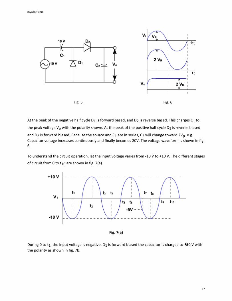
Fig. 5 Fig. 6
At the peak of the negative half cycle D1 is forward based, and D2 is reverse based. This charges C1 to
the peak voltage Vp with the polarity shown. At the peak of the positive half cycle D1 is reverse biased
and D2 is forward biased. Because the source and C1 are in series, C2 will change toward 2Vp. e.g. Capacitor voltage increases continuously and finally becomes 20V. The voltage waveform is shown in fig. 6.
To understand the circuit operation, let the input voltage varies from -10 V to +10 V. The different stages
of circuit from 0 to t10 are shown in fig. 7(a).
Fig. 7(a)
During 0 to t1, the input voltage is negative, D1 is forward biased the capacitor is charged to �10 V with the polarity as shown in fig. 7b.
mywbut.com
17
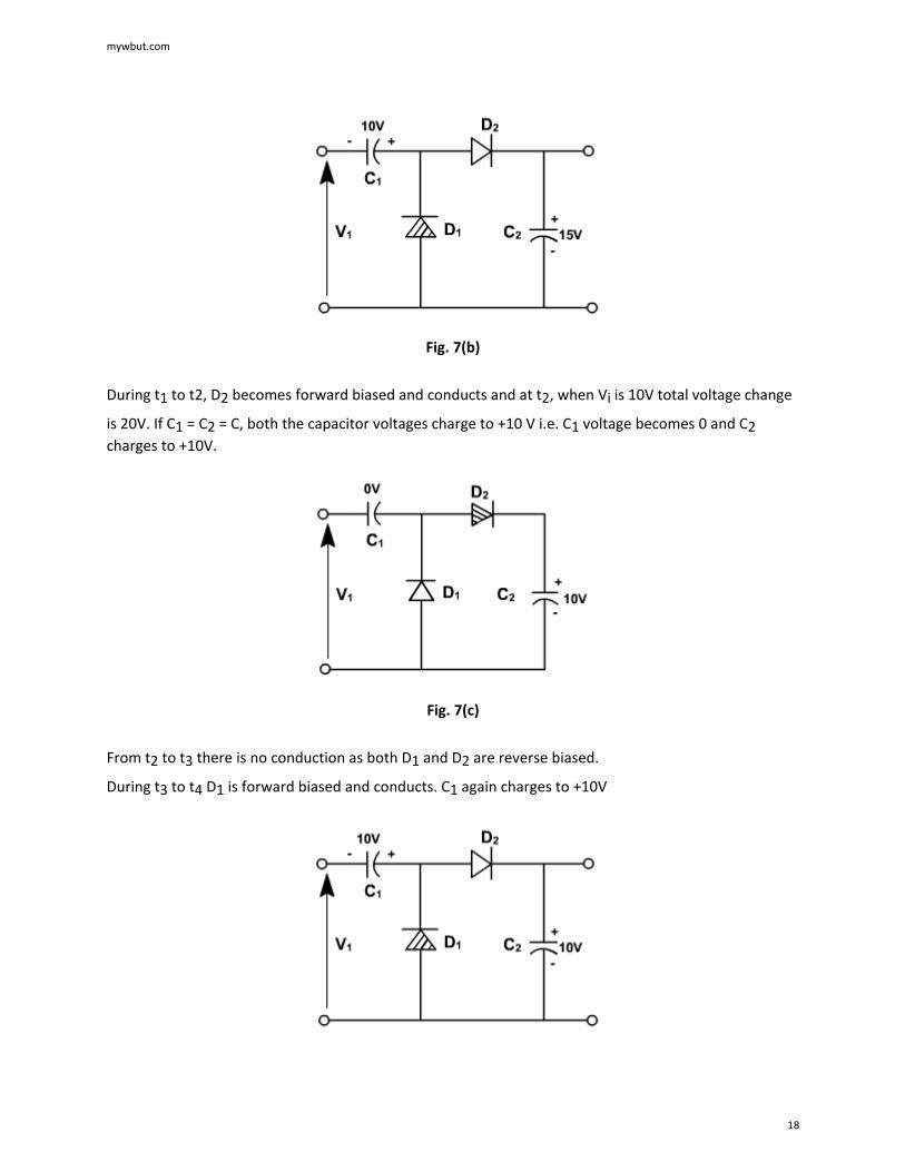
Fig. 7(b)
During t1 to t2, D2 becomes forward biased and conducts and at t2, when Vi is 10V total voltage change
is 20V. If C1 = C2 = C, both the capacitor voltages charge to +10 V i.e. C1 voltage becomes 0 and C2 charges to +10V.
Fig. 7(c)
From t2 to t3 there is no conduction as both D1 and D2 are reverse biased.
During t3 to t4 D1 is forward biased and conducts. C1 again charges to +10V
mywbut.com
18
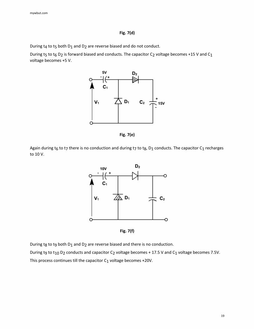
Fig. 7(d)
During t4 to t5 both D1 and D2 are reverse biased and do not conduct.
During t5 to t6 D2 is forward biased and conducts. The capacitor C2 voltage becomes +15 V and C1 voltage becomes +5 V.
Fig. 7(e)
Again during t6 to t7 there is no conduction and during t7 to t8, D1 conducts. The capacitor C1 recharges to 10 V.
Fig. 7(f)
During t8 to t9 both D1 and D2 are reverse biased and there is no conduction.
During t9 to t10 D2 conducts and capacitor C2 voltage becomes + 17.5 V and C1 voltage becomes 7.5V.
This process continues till the capacitor C1 voltage becomes +20V.
mywbut.com
19
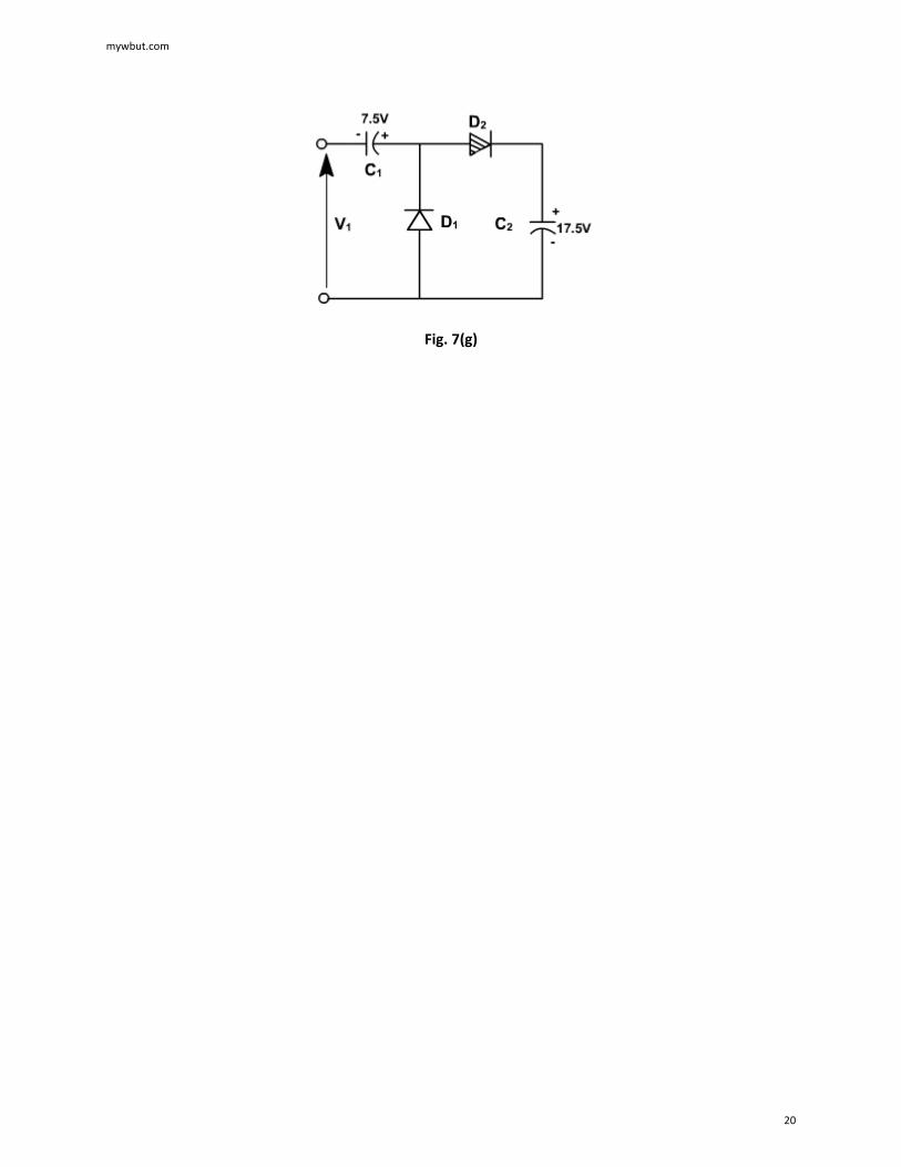
Fig. 7(g)
mywbut.com
20