Embed Size (px)
Citation preview
This is a repository copy of Automated background subtraction technique for electron energy-loss spectroscopy and application to semiconductor heterostructures.
White Rose Research Online URL for this paper:http://eprints.whiterose.ac.uk/107202/
Version: Accepted Version
Article:
Angadi, V. orcid.org/0000-0002-0538-4483, Abhayaratne, C. and Walther, T. orcid.org/0000-0003-3571-6263 (2016) Automated background subtraction technique for electron energy-loss spectroscopy and application to semiconductor heterostructures. Journal of Microscopy, 262 (2). pp. 157-166. ISSN 0022-2720
https://doi.org/10.1111/jmi.12397
[email protected]://eprints.whiterose.ac.uk/
Reuse
Unless indicated otherwise, fulltext items are protected by copyright with all rights reserved. The copyright exception in section 29 of the Copyright, Designs and Patents Act 1988 allows the making of a single copy solely for the purpose of non-commercial research or private study within the limits of fair dealing. The publisher or other rights-holder may allow further reproduction and re-use of this version - refer to the White Rose Research Online record for this item. Where records identify the publisher as the copyright holder, users can verify any specific terms of use on the publisher’s website.
Takedown
If you consider content in White Rose Research Online to be in breach of UK law, please notify us by emailing [email protected] including the URL of the record and the reason for the withdrawal request.

For Review O
nly
�
�
�
�
�
�
������������ ������������������������������������
���� ����������������������������������������������������������������
�
�
�������� �������������� �����
������ ������ ����������������
� ������������ �������� ��� �!�������"�����
�����#�$ ���!�$������%������ �&��
'� ������( ����)�%������� %�*�! +�,�����!��-�.� /��� ����)�#��)) ��!+������� �����)�0������� ����!�
0����� ����0�* ���� �*�%$���������+�'��� ��-�����.� /��� ����)�#��)) ��!+������� �����)�0������� ����!�0����� ����0�* ���� �*��������+���� ��-�.�/��� ����)�#��)) ��!+�000�
1��2��!���������������*�������������������+����������+�$��3*����!���$����� ��+����/��) �+�00(#�4���� ) ��� ��+� �� 5�� ����!*�+��������������� �* �*�
��
�
�
Journal of Microscopy

For Review O
nly
Automated Background Subtraction Technique for Electron Energy-loss Spectroscopy and
Application to Semiconductor Heterostructures
Veerendra C Angadi*, Charith Abhayaratne and Thomas Walther
†�
Dept. Electronic and Electrical Engineering, Sir Frederick Mappin Building,
University of Sheffield, Sheffield S1 3JD, UK.
Email: †[email protected] (corresponding author),
Key words
EELS quantification, background subtraction, ionization edge, core-loss, hyperspectral
imaging
Summary
Electron energy loss spectroscopy (EELS) has become a standard tool for identification and
sometimes also quantification of elements in materials science. This is important for
understanding the chemical and/or structural composition of processed materials. In EELS,
the background is often modelled using an inverse power-law function. Core-loss ionization
edges are superimposed on top of the dominating background, making it difficult to
quantify their intensities. The inverse power-law has to be modelled for each pre-edge
region of the ionization edges in the spectrum individually rather than for the entire
spectrum. To achieve this, the pre-requisite is that one knows all core-losses possibly
present. The aim of this study is to automatically detect core-loss edges, model the
background and extract quantitative elemental maps and profiles of EELS, based on several
EELS spectrum images (EELS SI) without any prior knowledge of the material. The algorithm
provides elemental maps and concentration profiles by making smart decisions in selecting
pre-edge regions and integration ranges. The results of the quantification for a
semiconductor thin film heterostructure show high chemical sensitivity, reasonable group
III/V intensity ratios but also quantification issues when narrow integration windows are
used without deconvolution.
Introduction
Electron energy-loss spectroscopy (EELS) can be used for identification and quantification of
light elements present in a material at near atomic or even atomic resolution. An EEL
spectrum consists of a zero-loss peak, band-edge transitions, plasmon and ionization edges
on top of a background which decays almost exponentially with energy for high energy-
losses. The ionization core-losses superimposed on this can be extracted using statistical
tools (Egerton, 1975, 2011b). However, the inverse power-law fails to model EELS in the
low-loss region (van Puymbroeck et al, 1992). The conventional method of quantification by
manually selecting a pre-edge region to extract ionization edges is exhaustive and leads to
inconsistency for thousands of spectra. State of the art software tools like Hyperspy (de la
Peña et al., 2015) and Gatan Digital Micrograph (Gatan, 2015) remove such inconsistency
partly by applying quantification routines to entire EELS SI data sets. Similarly, a model-
based approach to EELS quantification has been presented (Verbeeck & Van Aert, 2004).
Page 1 of 23 Journal of Microscopy

For Review O
nly
These authors later discussed standard-less quantification of EELS, which provided better
results (Verbeeck & Bertoni, 2008). None of these software packages, however, detects an
ionization edge and quantifies it automatically without any human intervention: Hyperspy
can perform an independent component analysis (de la Pena, 2011) but the physical
interpretation of the statistically significant components in terms of element-specific core
losses still needs to be provided by the user for any type of multivariate statistical analysis
(Walther and Trebbia, 1996). Digital Micrograph scripts such as Oxide Wizard (Yedra et al.,
2014) typically work on the basis of the user first assigning regions of interest and
identifying edges manually, which the algorithm can then track and quantify in similar
spectra of larger data sets. The aim of this study is to subtract the EELS background and
provide elemental maps and profiles of thousands of spectra or an extended SI without any
prior knowledge of the ionization edges.
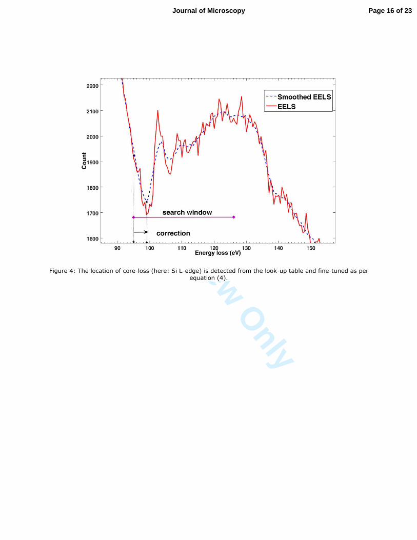
Description of the program
The process can be explained in two parts: ionization core-loss edge detection and
background subtraction for detected individual ionization edges. The quantification of EELS
used in our approach is by the standard integration method (Egerton, 1978). To quantify a
spectrum there are a lot of challenges in terms of artifacts, noise and gain correction
problems of the charged couple device (CCD) camera. Hence, a pre-treatment of spectra is
necessary before the process of edge detection and background subtraction. If the
background is exponentially decaying, there is no ionization edge and the signal-to-noise-
ratio (SNR) is high, then the gradient of the spectrum should be negative everywhere. As the
spectrum is pre-processed, positive gradients indicate the presence of core-loss edges. A
look-up table is used to accurately identify the corresponding core-losses of the elements.
An inverse power-law is used to fit a curve in the pre-edge region to subtract the
background. The extracted core-loss edges are used for further quantification using
integration after background subtraction. All programming was performed in Matlab using
the current version, R2015b.
Data pre-processing
The noise in a spectrum arises due to a combination of low electron count numbers and
read-out noise of the CCD camera (Ishizuka, 1993). The objective is to detect the core-loss
edges after the acquisition of the spectrum image in the presence of noise. The noise in the
spectra is a mixture of Poisson noise (or shot noise) and Gaussian noise (de la Pena, 2010).
The ionization cross-section decreases with increasing energy loss. As the signal-to-noise-
ratio (SNR) decreases with energy-loss, the intensity of high-loss ionization edges becomes
comparable to the noise level. This emphasises the necessity of pre-processing signals
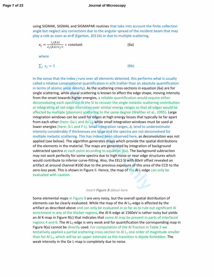
before calculating the gradient of the spectra. An averaging filter is always inefficient (Boyle
& Thomas, 1988; Davies, 1997; Justusson, 1981) as it does not consider the type of noise
and spikes (or pulses) are not completely removed (Figure 1). The number of spectral
channels selected as filter width, w, influences the residual noise after smoothing but will
also suppress the core-loss signal to some degree, in particular for sharp edges. An
averaging filter gives good noise suppression when multiple spectra are averaged, providing
a collective representative spectrum with reduced noise. Principle component analysis (PCA)
is a form of multivariate analysis, using orthogonal eigenfunctions (Fukunaga, 1990; Jolliffe,
Page 2 of 23Journal of Microscopy

For Review O
nly
2002; Pearson, 1901; Manly, 2004). A multivariate analysis tool (simply called PCA function
in Matlab R2015b) has been used to analyse datasets in an unsupervised manner. The
dataset in this case is the SI. The components of the PCA are spectral components ranked in
order of significance. The lower order components with high variance represent all the
components needed to describe most features of the spectrum apart from the noise (low
variance). Hence, PCA can in principle be used for denoising the spectrum, and a Poisson-
weighted PCA algorithm that properly accounts for the variance in shot noise has been used
to reduce noise in Time-of-Flight Secondary Ion Mass Spectrum images (Keenan and Kotula,
2004). If the noise is Poissonian however, a morphological filter such as a median filter is the
most effective way of improving the SNR, as shown in Figure 1. In 2-D (images), a median
filter has been proven to be best filter in case of ‘salt and pepper noise’, which corresponds
to Poisson noise in images (Lim, 1990; Pratt, 2007). Here, it preserves the shape of the
spectrum. Figure 1 shows the performance of different filters in terms of removing artificial
spikes in a spectrum with a delayed In M-edge from InGaAs. As the SNR is decreasing with
energy almost exponentially, a median filter is chosen as defined in equation (1).
�� = exp�median ln ����� (1)
where S is the spectrum, w is a window over which the median filter is applied. In the
following, all spectra were median filtered first to help identify the core-loss edges, then the
quantification routines for background fit, extrapolation and signal integration were applied
to the unfiltered spectra. Filtering will not remove noise due to CCD gain inconsistencies.
This can lead to false positive identification of apparent ionization edges.
Insert Figure 1 about here
Detection of ionization core-loss edges
For automation of background subtraction, a novel approach of core-loss edge detection is
proposed. The gradient of the EELS SI in the direction of energy-loss is determined by
equation (2).
∇�� = ���
���� (2)
where ∇�� is the gradient of the SI (data cube) with regard to spatial ��, �� directions and
energy-loss direction��. The gradient of EELS has to be negative for ranges beyond multiple
plasmon losses and without any core-losses. The only points that are positive must be due
to the presence of noise or ionization edges. If the EELS SI is de-noised, the probability of
positive gradient being noise is low, although clearly dependent on the type of denoising
method used. The angle (�) between the EELS and horizontal energy axis is determined by
equation (3) and can be plotted, as shown for an example spectrum of silicon with carbon in
Figure 2.
Insert Figure 2 about here
� = arctan "��� �� (3)
Only positive angles are considered further as negative values are due to the background of
EELS. A cluster of positive angles is formed if a core-loss edge is present. Positive angle
values without a cluster are due to noise. Clusters are detected by counting the positive
Page 3 of 23 Journal of Microscopy

For Review O
nly
angular data points that are comparable to the size of a window. The flow chart for the
process implemented in Matlab is shown in Figure 3.
Insert Figure 3 about here
The size of the window is chosen such that it should be comparable to the sharpness of the
onset of typical edges (a few eV for sharp hydrogenic and up to 10eV for delayed edges).
Similarly, the window size should not be too small (<5 channels), to avoid false positives due
to noise. Typically, the window sizes selected are between 5 to 20 channels wide (the
default is w=15), and clusters are identified as intervals of that given width wherein at least
2/3 of all channels have angular values θ>0.
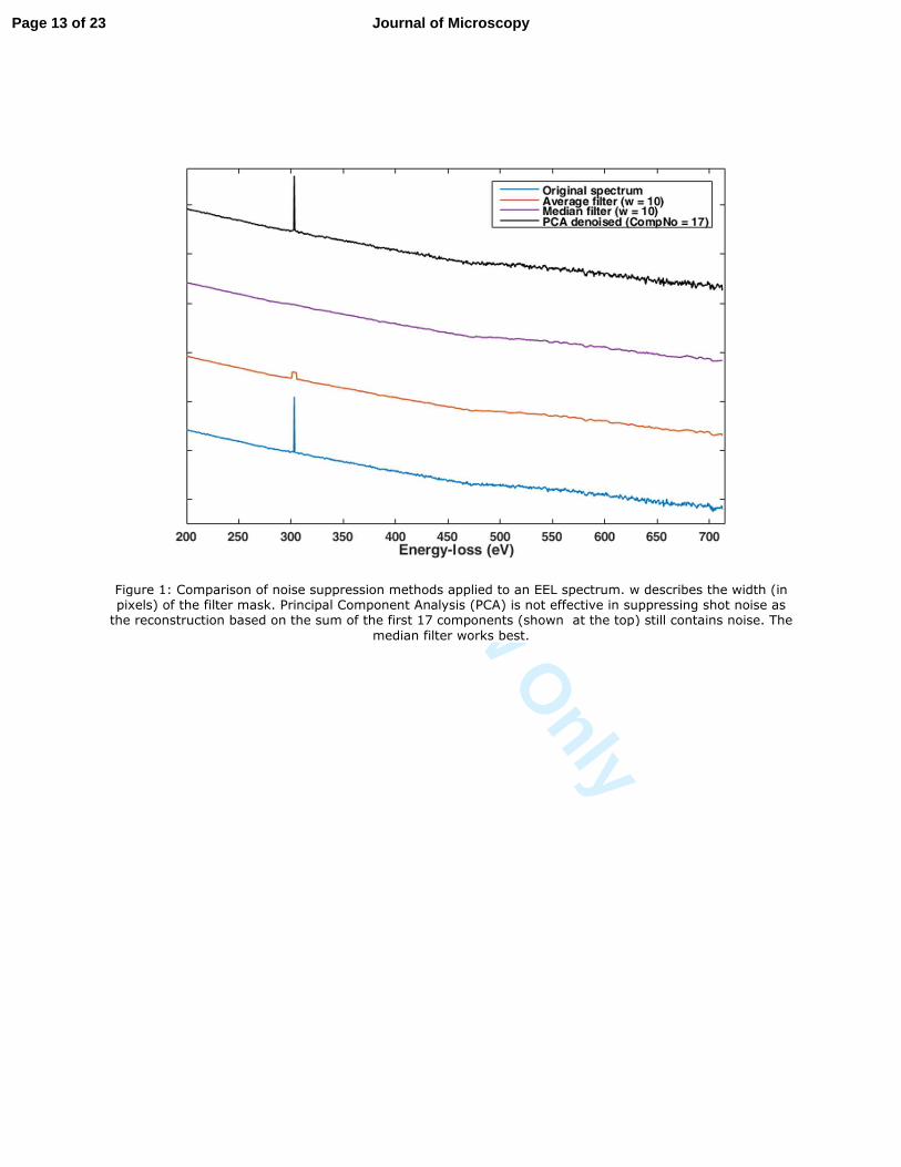
Due to near edge structures or/and chemical shifts the edges detected may not be at the
exact location of the ionization onset predicted for free atoms. It may also happen that 2 or
3 consecutive windows might detect positive angles. To refine the results from ionization
edge identification, a look-up table is used containing onset values of all major ionization
edges (Ahn et al, 1983; Egerton, 2011b). The shape of the edges is also considered during
quantification, as discussed later. The exact edge onset is identified from the predicted
edges (clusters) by finding the nearest ionization edge in the look-up table, as shown in
equation (4):
�#$%& = � '() ‖�+,-./01234‖5� (4)
where En is the list of all n ionization edges from the look up table, Clusteri is the list of all
predicted ionization edge onsets (numbered consecutively by index). The ionization edge
detection and correction can be visualized as shown in Figure 4.
Insert Figure 4 about here
Histograms of the detected edges in three different EELS SI of a cross-sectioned multi-
junction solar cell are shown in Figure 5. While edge onset identification may fail in
individual spectra due to noise the histograms clearly show that the identification of the
edges is unambiguous when thousands of spectra from all locations in SI are considered.
The efficiency of the edge detection is also dependent on the quality of the gain correction
of the CCD. Long exposures of the zero-loss peak might yield artifacts in successively
acquired spectra due to gain changes induced by over exposures. This could potentially lead
to false positive detection of ionization edges in EELS acquired with energy offsets. Such
artifacts can, however, be identified by varying the energy offset as they remain fixed at
that channel (usually around # 100) where the zero-loss peak had been before.
Insert Figure 5: about here
Curve-fitting
The presence of the zero-loss peak and plasmon losses in low loss spectra makes it difficult
to model the background for energies below about 100eV. The inverse power-law is used to
Page 4 of 23Journal of Microscopy

For Review O
nly
model the background in pre-edge regions for individual ionization core-loss edges above
this threshold. This may be justified in our case as Table 1 demonstrates we have generally
used high dispersions for lower energy losses and lower dispersions at higher offsets so that
wide regions with low energy losses, wherein the shape of the core-loss background often
departs significantly from the slope expected from a simple inverse power-law function
(Leapman, 2005), have been avoided. A linear model of ionization edges superimposed on a
background modelled by an inverse power-law at higher losses is considered as shown in
equation (5).
�6%789:; = <�,3 + ∑ �&?&,A&,A (5)
where A and r are the inverse power-law curve fitting parameters for energy-loss (E), � is the
intensity and σ the ionization the cross-section for the jth
shell of ith
element in the
spectrum.
The pre-edge regions for the background modelling should be selected as large as possible
to minimize systematic errors. A larger pre-edge region provides more data points for
modelling of the background and chemical shifts that could shift the edge onset by up to
~8eV are less prone to influence the background modelling. Due to the possible presence of
near edge structure, the pre-edge region should ideally end well before the edge onset.
Hence the pre-edge region is selected dynamically by the algorithm over all the core-loss
edges and across the EELS SI. The pre-edge region extends typically from half the distance
between two consecutive core-loss edges to a few channels before the nominal edge onset.
Standard integration methods are used for the quantification of background subtracted EEL
spectra (Egerton, 1978). If the integration window exceeded the experimental energy-loss
axis limit then the edge would be omitted (in the semiconductor multilayer example
presented later, the integration window for the P L3 edge was manually reduced to 37.4eV
to avoid this). The selection of integration window and the systematic and statistical errors
influencing quantification have been discussed by Leapman (2005). Two core-loss edges
close to each other will be partially overlapping and are not accurately quantifiable by this
integration method. The accuracy of the quantification also depends on the shape of the
ionization edges. If the onset of an ionization edge is delayed, small integration windows
give high statistical errors. Hence the initially specified integration window (∆) is applied
only to hydrogenic edges. In case of delayed edge onsets, the spectrum is integrated up to
the next ionization edge onset, providing better statistics for delayed maximum edge shapes
but at the cost of slightly higher systematic errors. EELS is usually performed with a
spectrometer entrance aperture, and the integration of the spectrum intensity is a function
of collection angle (β) and integration window (∆) (Egerton, 2011b). The values of partial
cross-sections are evaluated from the SIGMAK3, SIGMAL3 and SIGPAR Matlab routines
written by Egerton (2011a). The overall process of core-loss edge selection and background
subtraction is shown in the form of a block diagram in Figure 6.
Insert Figure 6 about here
Experimental
Four EELS SI using different energy offsets and dispersions were acquired from the same
area of a cross-sectioned semiconductor heterostructure designed to be used for multi-
junction solar cells. On top of a germanium substrate (not shown due to limited field of
Page 5 of 23 Journal of Microscopy

For Review O
nly
view) several GaAs-based layers of different thicknesses had been deposited. The SIs have
been acquired in a JEOL 2010F field emission transmission electron microscope operated in
STEM mode at 197kV and equipped with a Gatan Imaging Filter (GIF200) with parameters as
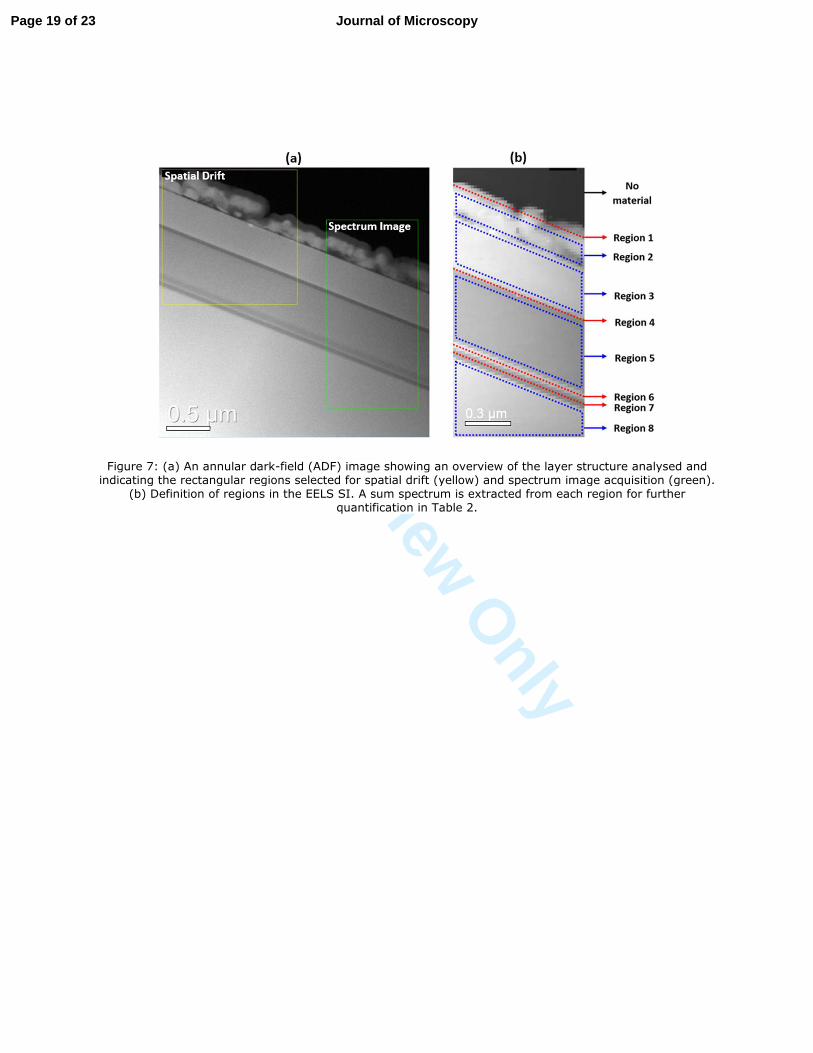
shown in Table 1. Figure 7(a) is an annular dark-field (ADF) overview image of the
heterostructure obtained with 55-170 mrad collection angle in which the spectrum image
and spatial drift regions used are indicated. The SI shows 8 distinctive regions as labelled in
Figure 7(b). The thicker layers labelled by numbers 3, 5 and 8 clearly differ in their scattering
power due to their different chemistry, which we want to investigate in this study, and the
top regions (1 & 2) consist of nano-crystals that appear to overlap in projection or are
sintered together and were deposited to further improve the coupling to the incoming light.
EELS SI_0 EELS SI_1 EELS SI_2 EELS SI_3
SI size [pixels] 90 x 44 x
1024
45 x 22 x
1024
90 x 44 x
1024
92 x 43 x
1024
real-space pixel size [nm] 24.4 48.8 24.4 23.9
dispersion [eV/channel] 0.2 0.1 0.5 1
nominal magnification 20000 20000 20000 20000
conv. angle (α) [mrad] 16.6 16.6 16.6 16.6
coll. angle (β) [mrad] 15 15 15 15
spectrum offset [eV] 0 80 250 950
exposure time [sec] 0.1 0.5 0.5 2
total acquisition time
[min]
9 11 44 176
Table 1: EELS data acquisition parameters for the four spectrum images (SI) acquired from
the same area, indicated by the green rectangle in Figure 6(a). Actual acquisition
commenced in reverse order, starting with the highest energy losses. The SI sizes give pixel
numbers along x- and y-directions and channel number along the energy-loss coordinate.
Acceleration voltage: 197kV
Insert Figure 7 about here
Results from a test case of a semiconductor heterostructure
Sum spectra are extracted from each individual region for quantification. Elemental
concentrations (x) are calculated using equation (6a) where the constant is chosen such that
the concentrations of all detected elements sums up to unity in equation (6b).
Quantification results for each region are shown in Table 2. Specimen thickness (t) values in
terms of multiples of the mean free path (λ) of inelastic scattering can be extracted from the
first EELS Si which contains the zero loss and plasmon peaks. These t/λ values are
approximately 1 (except in the top thin layer of region 1) indicating an average specimen
thickness around t≈130nm, which corresponds to the inelastic mean free path calculated
according to Egerton (2011b) for GaAs under the conditions listed in Table 1.
The values in Table 2 are normalised with respect to thickness (t/λ) and exposure time (τ).
The parameters in Table 1 are used for the calculation of partial cross-sections, σ (β, ∆),
Page 6 of 23Journal of Microscopy
For Review O
nly
using SIGMAK, SIGMAL and SIGMAPAR routines that take into account the finite collection
angle but neglect any corrections due to the angular spread of the incident beam that may
play a role as soon as α>β (Egerton, 2011b) or due to multiple scattering.
�A =�B C,∆�
EB C,∆�∗1B∗G×constant (6a)
where
∑ �A = 1A (6b)
In the sense that the index j runs over all elements detected, this performs what is usually
called a relative compositional quantification in at% (rather than an absolute quantification
in terms of atomic areal density). As the scattering cross-sections in equation (6a) are for
single scattering, while plural scattering is known to affect the edge shape, moving intensity
from the onset towards higher energies, a reliable quantification would require either
deconvoluting each spectrum in the SI to recover the single inelastic scattering contribution
or integrating all net edge intensities over similar energy ranges so that all edges would be
affected by multiple (plasmon) scattering to the same degree (Walther et al., 1995). Large
integration windows can be used for edges at high energy losses that typically lie far apart
from each other (here: Ga L and As L), while small integration windows must be used at
lower energies (here: Si L and P L). Small integration ranges, Δ, tend to underestimate
intensity considerably if thicknesses are large and the spectra are not deconvolved for
multiple inelastic scattering. This has indeed been observed here, as deconvolution was not
applied (see below). The algorithm generates maps which provide the spatial distributions
of the elements in the material. The maps are generated by integration of background
subtracted spectra at each point according to equation (6a). The background subtraction
may not work perfectly for some spectra due to high noise or near edge structures which
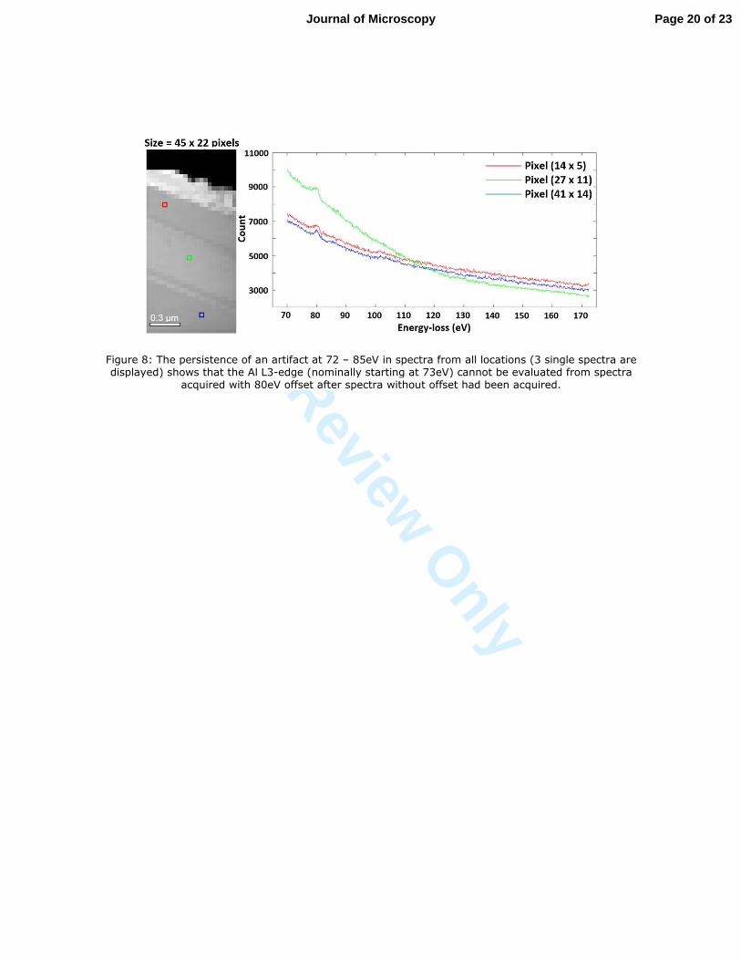
would contribute to inferior curve-fitting. Also, the EELS SI with 80eV offset revealed an
artifact at around channel #100 due to the previous exposure of this area of the CCD to the
zero-loss peak. This is shown in Figure 8. Hence, the map of the Al L-edge can only be
evaluated with caution.
Insert Figure 8 about here
Some elemental maps in Figure 9 are very noisy, but the overall spatial distribution of
elements can be clearly evaluated. While the map of the Al L3-edge is affected by the
artifact as described above and can only be evaluated in so far as to rule out significant Al
enrichment in any of the thicker regions, the Al K-edge at 1560eV is rather noisy but yields
an Al K-map in Figure 9(c) that indicates that some Al may be present in parts of interfacial
regions 4 and 6. The Al L1-edge is very weak and for quantification the corresponding map in
Figure 9(a) cannot be directly used. For computation of the Al fraction in Table 2 we
tentatively applied a partial scattering cross-section to Al L1 one order of magnitude smaller
than for Al L3, which will be an upper estimate as this transition is dipole-forbidden. The
weak intensity in the Ge L-map is completely due to noise.
Page 7 of 23 Journal of Microscopy

For Review O
nly
The quantification of individual spectra generally lacks statistics due to noise. Considering
instead the sum of spectra from sub-regions as labelled in Figure 7(b) not only provides
better SNR but a computationally viable method for quantification. Each inclined row
marked by red lines in Figure 7(b) consists of 24 spectra (for EELS SI_1) or 47 spectra (for all
other SIs), while the wider regions numbered 2, 3, 5 and 8 all contain several hundred
spectra.
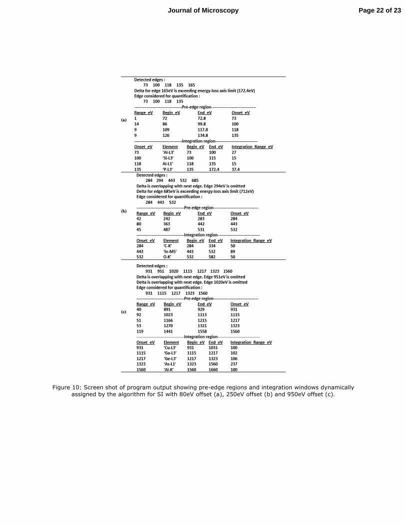
Screen shots of the program outputs are shown in Figures 9 and 10. It can be observed that
the algorithm automatically detects the core losses and dynamically selects pre-edge
regions and integration windows for each core-loss of the SI and that the output maps yield
a quick visual feedback on the relative strengths of the chemical signals detected.
Neglecting the signals from C (main surface contamination) and O (due to surface oxidation)
the nominal values from Table 2 for wider regions 3, 5 and 8 would indicate chemical
compositions of the underlying compound semiconductors of GaAs0.84P0.16:Si,
Al0.09In0.37Ga0.54P:As and GaAs:P,Si respectively, where the elements listed after the colon
refer to minority elements in the detection range of 1-2 at%, which however seems
somewhat high for dopants. If we check the ratio of group III/ group V elements in these
three compounds, i.e. (xAl+xIn+xGa)/(xP+xAs), the values of 1.06, 1.04 and 0.91 obtained from
the above three regions are in reasonably good agreement with the expected value of unity
for a stoichiometric III/V compound semiconductor. As previously stated, the proposed
method is mainly a demonstration of automated background subtraction by identifying
core-losses, and plural scattering is not presently taken into account in Table 2. The effect
from plural scattering could be pronounced for Al, Si and P L2,3-edges as these display
slightly delayed onsets while the integration ranges are small. Hence the effect of plural
scattering will move intensity from the edge onsets to values beyond the range of the actual
EELS measurement (for P) or the integration range (for Al and Si), so the intensities in the
experiment may be significantly lower than the cross-sections calculated for single
scattering predict. A quick estimate based on the small widths of the integration ranges
used here (15 eV for Al and Si, and 37.4eV for P) relative to the plasmon energy of GaAs
(~16eV) shows that plural scattering could reduce intensities of the Al and Si L edges by
factors of up to 2 for t/λ≈1, however, the concentrations for Al and Si are rather low anyway
and so the precise values are perhaps not so relevant, while the effect on the P L2,3 edge will
be much weaker. The effect of plural scattering could in principle be minimised by
deconvolution with the low loss spectrum, which we will explore in the future. The
identification of the chemical composition in the smaller regions is strongly limited by
counting statistics as well as a potential undersampling of the thinnest layers given the pixel
sizes reported in Table 1. The implementation of the algorithm in Matlab R2015b means the
code can be distributed not only to multiple processing cores (presently a PC with 2 cores is
used) but to multiple computers using the Matlab parallel computing tool box.
Insert Figure 9 about here
Insert Figure 10 about here
Page 8 of 23Journal of Microscopy

For Review O
nly
�80eV offset 250eV offset 950eV offset
�t/λ Si L3 Al L1 P L3 C K In M4,5 O K Cu L3 Ga L3 As L3
dispersion
(eV/channel) 0.10 0.10 0.10 0.50 0.50 0.50 1.00 1.00 1.00
τ (sec) 0.50 0.50 0.50 0.50 0.50 0.50 2.00 2.00 2.00
∆ (eV) 15 15 37.4 50 89 50 200 200 200
region 1 0.52 1.44 3.22 5.47 44.09 2.37 43.40 0.00 0.00 0.00
region 2 0.96 1.51 2.08 3.89 30.03 0.00 38.30 24.18 0.00 0.00
region 3 0.95 7.87 0.00 6.26 9.29 0.00 2.41 0.00 41.46 32.72
region 4 0.95 8.53 1.63 40.73 18.61 10.37 0.00 0.00 10.07 10.05
region 5 1.01 0.00 3.99 43.48 10.10 16.90 0.00 0.00 25.02 0.50
region 6 1.04 3.82 1.62 29.97 4.84 3.61 0.00 0.00 22.80 33.35
region 7 1.04 1.57 3.17 49.16 7.87 19.08 0.00 0.00 8.92 10.23
region 8 1.11 8.07 0.00 1.92 0.00 0.00 1.50 0.00 42.94 45.57
Table 2. Quantification in at% of each region of the four Sis recorded. The sum of all
concentrations has been normalised to 100% according to equation (6b).
Conclusion
The algorithm is robust in detecting ionization edges. Mapping of the core loss intensity is
provided for quantitative assessment of sub-regions. Quantification can be done from
spectra integrated over each sub-region. The ionization edges at low energies or edges
which are very close to each other are always difficult to quantify as the background is
difficult to subtract. Inconsistencies in gain correction of the detector are not taken into
account in edge detection and background subtraction. Hence, a false positive identification
of edges is possible at around channel #100 or more generally in the presence of excessive
noise. The elemental maps produced by the proposed algorithm are in qualitative
agreement with results from Gatan Digital Micrograph. The noise present in elemental maps
can be reduced by applying image processing techniques. The effects from plural scattering
have not been taken into account for quantification as yet but this needs to be done in the
future and a graphical user interface is also in development.
Page 9 of 23 Journal of Microscopy

For Review O
nly
References
Ahn, C.C., Burgner, R.P. & Krivanek, O.L. (1983) EELS Atlas: a reference guide of electron
energy loss spectra covering all stable elements: Center for Solid State Science,
Arizona State University, USA.
Boyle, R.D. & Thomas, R.C. (1988) Computer vision: a first course: Blackwell Scientific,
Oxford, UK.
Davies, E.R. (1997) Machine Vision: Theory, Algorithms and Practicalities. 2nd
ed, Academic
Press. New York, pp77-99.
de la Peña, F. (2010) Advanced methods for Electron Energy Loss Spectroscopy core-loss
analysis. PhD thesis, Université de Paris-Sud, Paris.
de la Peña, F., Berger, M.-H., Hochepied J.-F., Dynys F., Spephan O. & Walls M. (2011)
Mapping titanium and tin oxide phases using EELS: An application of independent
component analysis. Ultramicroscopy 111, pp 169-176.
de la Peña, F. et al (2015) hyperspy: HyperSpy 0.8.1. Retrieved from http://hyperspy.org/,
Date: 22/10/2015.
Egerton, R.F. (1975) Inelastic scattering of 80 keV electrons in amorphous carbon.
Philos.Mag. 31, pp199-215.
Egerton, R.F. (1978) Formulae for light-element micro analysis by electron energy-loss
spectrometry. Ultramicroscopy 3, pp243-251.
Egerton, R.F. (2011a) Computer Programs for Electron Energy-Loss Spectroscopy in the
Electron Microscope. Retrieved from http://www.tem-eels.ca/computer-
programs/index.html, Date: 22/10/2015.
Egerton, R.F. (2011b) Electron energy-loss spectroscopy in the electron microscope, 3rd
edition, Springer, New York.
Fukunaga, K (1990). Introduction to statistical pattern recognition. 2nd
edition, Academic
Press, New York.
Gatan (2015) Gatan Microscopy Suite Software. Retrieved from
http://www.gatan.com/products/tem-analysis/gatan-microscopy-suite-software,
Date: 22/10/2015.
Ishizuka, K. (1993) Analysis of Electron Image Detection Efficiency of Slow-Scan CCD
Cameras. Ultramicroscopy 52, pp7-20.
Jolliffe, I (2002). Principal Component Analysis and Factor Analysis: Principal Component
Analysis, 2nd
edition, Springer, New York, pp150-166.
Justusson, B.I. (1981) Two-dimensional digital signal processing II: transforms and median
filters. Median filtering: statistical properties, Springer, Berlin, pp161-196.
Keenan, M.R. & Kotula, P.G (2004) Accounting for Poisson noise in the multivariate analysis
of ToF-SIMS spectrum images. Surface Interface Anal. 36, pp 203-212.
Leapman, R. (2005) EELS Quantitative Analysis Transmission Electron Energy Loss
Spectrometry in Materials Science and The EELS Atlas, 2nd
edition, Wiley-VCH,
Weinheim, pp49-96.
Lim, J.S. (1990). Two-dimensional signal and image processing. Prentice Hall, Englewood
Cliffs, New Jersey.
Pearson, K. (1901) On lines and planes of closest fit to systems of points in space.
Philos.Mag. Series 6, 2, pp559-572.
Pratt, W.K. (2007). Geometrical Image Modification, in: Digital Image Processing, 4th
edition,
Wiley, New Jersey, pp386-393.
Page 10 of 23Journal of Microscopy

For Review O
nly
Manly, B.F.J. (2004). Multivariate Statistical Methods: A Primer, 3rd
edition, CRC Press,
Florida, USA.
van Puymbroeck, J., Jacob, W. & van Espen, P. (1992) Methodology for spectrum evaluation
in quantitative electron energy-loss spectrometry using the Zeiss CEM902. J.
Microsc. 166, pp273-286.
Verbeeck, J. & Bertoni, G. (2008). Model-based quantification of EELS: is standardless
quantification possible? Microchimica Acta 161, pp439-443.
Verbeeck, J. & Van Aert, S. (2004) Model based quantification of EELS spectra.
Ultramicroscopy 101, pp207-224.
Walther, T., Humphreys, C.J., Cullis, A.G. & Robbins, D.J. (1995) A correlation between
compositional fluctuations and surface undulations in strained layer epitaxy.
Material Science Forum 196-201, pp. 505-510.
Walther T. & Trebbia P. (1996) Maxwell's demon and data analysis — Discussion. Philos.
Trans. Roy. Soc. Lond. A 354, pp 2709-2711.
Yedra, L., Xuriguera, E., Estrader, M., Lopez-Orteag A., Baro, M.D., Nogues, J., Roldan, M.,
Varela, M., Estrade, S. & Peiro, F. (2014) Oxide Wizard: An EELS application to
characterize the white lines of transition metal edges. Microsc. Microanal. 20, pp 698-
705.
Page 11 of 23 Journal of Microscopy

For Review O
nly
Figure captions
Figure 1: Comparison of noise suppression methods applied to an EEL spectrum. w describes
the width (in pixels) of the filter mask. Principal Component Analysis (PCA) is not effective in
suppressing shot noise as the reconstruction based on the sum of the first 17 components
(shown at the top) still contains noise. The median filter works best.
Figure 2: Original spectrum of Si L-edge and C K-edge (in dark blue) and angle as defined in
equation (3) (in red) showing the presence of clusters in the latter correlates with the onset
of ionization edges.
Figure 3: Flow chart for edge detection in spectra that consist of 1024 channels. c=count of
channels with positive gradient, i=energy channel, j=loop count, w= window width, mod =
modulo operator (remainder after division).
Figure 4: The location of core-loss (here: Si L-edge) is detected from the look-up table and
fine-tuned as per equation (4).
Figure 5: Histogram distribution of edge onsets detected for EELS SI from semiconductor
heterostructure shown in Figure 7 for 80eV offset (a), 250eV offset (b) and 950eV offset (c).
The edges are later identified in Table 2.
Figure 6: Block diagram of ionization core-loss edge selection and background subtraction.
Figure 7: (a) An annular dark-field (ADF) image showing an overview of the layer structure
analysed and indicating the rectangular regions selected for spatial drift (yellow) and
spectrum image acquisition (green). (b) Definition of regions in the EELS SI. A sum spectrum
is extracted from each region for further quantification in Table 2.
Figure 8: The persistence of an artifact at 72 – 85eV in spectra from all locations (3 single
spectra are displayed) shows that the Al L3-edge (nominally starting at 73eV) cannot be
evaluated from spectra acquired with 80eV offset after spectra without offset had been
acquired.
Figure 9: Set of maps generated with EELS SI of 80eV offset (a), with 250eV offset (b) and
with 950eV offset (c). The elemental maps show the spatial distribution of Al L3, Si L3, Al L1, P
L3, C K, In M4,5, O K, Cu L3, Ga L3, Ge L3, As L3 and Al K edges. Al L3 is a false positive detection
due to an artifact. Maximum intensity values in kilo-counts after background subtraction,
integration and scaling according to equation (6a) with constant=1.
Figure 10: Screen shot of program output showing pre-edge regions and integration
windows dynamically assigned by the algorithm for SI with 80eV offset (a), 250eV offset (b)
and 950eV offset (c).
Page 12 of 23Journal of Microscopy
For Review O
nly
��
�
�
����������� ������������������ ����������������� ���������������� ���������������������������������� ��������������������������� ����� ����� ������!���"����� !����������������#������� ������������������������������������������������������������������������$���� ������������������������ ������������������������%���
���������������������������
�
�
Page 13 of 23 Journal of Microscopy

For Review O
nly
��
�
�
��������������� ���������������������������������������������� ����������� �������������������������� ������������!�"�����!��������������� �����������!�� ����������� �����"��!��!���������������#�����������$��
�
�
Page 14 of 23Journal of Microscopy

For Review O
nly
��
�
�
������������� ������������������ ����������� ��������� ��������������� �������� � �������� ���������������������������������������� ������������� ����������������������� ����� ��������������!�� �������
��������������"���
�
�
Page 15 of 23 Journal of Microscopy
For Review O
nly
��
�
�
������������� ���� �� ��� ���� ���������������������������������� ������� ��������������������������������������� ��������
�
�
Page 16 of 23Journal of Microscopy

For Review O
nly
��
�
�
������������ ��������������� �� ������� ���������������� ������������ ������� ����� ������� ������������ ���������������� ������� �������� !�"����� �������� �����#����� �������� $�%�������������&�������������������
%��&��"$��
�
�
Page 17 of 23 Journal of Microscopy
For Review O
nly
����������� ������������������������ ������������������ ����������� �������������� �������
Page 18 of 23Journal of Microscopy
For Review O
nly
��
�
�
������������ ��������������������� ����������������������������������������������������������������������������������������������������������������������������������������������������������������������������� �
!�������������������������������""#$�$% � ������������������&�������������������������������������������������������'�!���( ��
�
�
Page 19 of 23 Journal of Microscopy
For Review O
nly
��
�
�
��������������� � ������������������������������������� ������������������������ ���� ������ ������������� �������� �� ����������!��"�#���������������� ������������������������$���%������������� �������
��&������ �����'������ ��������� ������� ���������� �������$������&�����(��
�
�
Page 20 of 23Journal of Microscopy

For Review O
nly
��
�
�
������������� ���������������������������� ������� ��������������� ����� �����!������������ ����� �����"�#�$����%������%���������������������%�������!������� �&%��'�����'��&%��(��)��'��*�+�����,-� ��.�+��*���'��/���'��/���'��&���'�����&%�+������#�&%��'������ �%���������0������"������������������� �"�#�,�1�����
��������2�0�%�������3�%�4"������� ����!�"3���������!���"�����������������������"�%�����""�����������5��������6��������"�������7(#��
�
�
Page 21 of 23 Journal of Microscopy
For Review O
nly
��
�
�
�������������� ����������������������������� ���������������� ��� ��� �������� ��� ������� �������������� ��������������������������������������������� !�"#������������ �� ��$#������������ %��
�
�
Page 22 of 23Journal of Microscopy
For Review O
nly
1
Lay Summary
Electron energy loss spectroscopy (EELS) has become a standard tool for identification and
sometimes also quantification of elements in materials science. This is important for
understanding the chemical and/or structural composition of processed materials. In EELS,
the background is often intense and can be modelled over small energy ranges using an
inverse power-law function. On top of this background, core-loss edges are superimposed
that are due to the ionization energies characteristic of each element. This study describes a
Matlab algorithm to automatically detect and quantify core-loss edges based on a single
inelastic scattering approach, without any prior knowledge of the material. The algorithm
provides elemental maps and concentration profiles by making smart decisions in selecting
pre-edge regions and integration ranges. Deconvolution to take into account plural
scattering is not considered yet but will be integrated in a future version.
Page 23 of 23 Journal of Microscopy


![DAF TAR PUSTAKA - scholar.unand.ac.idscholar.unand.ac.id/45709/4/DAFTAR PUSTAKA.pdf · [5] Soumya Jolad, Shridhar,“Speech Enhancement Using Spectral Subtraction Technique with Minimized](https://img.pdfslide.us/doc/110x75/5ff2bdb56effd4164178f592/daf-tar-pustaka-pustakapdf-5-soumya-jolad-shridharaoespeech-enhancement.jpg)