Embed Size (px)
Citation preview
This article appeared in a journal published by Elsevier. The attachedcopy is furnished to the author for internal non-commercial researchand education use, including for instruction at the authors institution
and sharing with colleagues.
Other uses, including reproduction and distribution, or selling orlicensing copies, or posting to personal, institutional or third party
websites are prohibited.
In most cases authors are permitted to post their version of thearticle (e.g. in Word or Tex form) to their personal website orinstitutional repository. Authors requiring further information
regarding Elsevier’s archiving and manuscript policies areencouraged to visit:
http://www.elsevier.com/copyright
Author's personal copy
Germanium films with strong in-plane and out-of-plane textureon flexible, randomly textured metal substrates
V. Selvamanickam a,�, S. Sambandam b, A. Sundaram a, S. Lee a, A. Rar b, X. Xiong b, A. Alemu c,C. Boney c, A. Freundlich c
a Department of Mechanical Engineering and Texas Center for Superconductivity, University of Houston, 4800 Calhoun Road, Houston, TX 77204, USAb SuperPower Inc., 450 Duane Avenue, Schenectady, NY 12304, USAc Center for Advanced Materials and Department of Physics, University of Houston, Houston, TX 77204-5004, USA
a r t i c l e i n f o
Article history:
Received 5 July 2009
Received in revised form
22 August 2009
Accepted 29 August 2009
Communicated by P. RudolphAvailable online 6 September 2009
PACS:
81.05.Cy
81.15.Jj
81.15.Kk
68.55.jm
81.15.Cd
Keywords:
A1. Texture
A3. Ion beam-assisted deposition
A3. Vapor phase epitaxy
B2. Photovoltaic materials
B2. Semiconducting germanium
B2. Semiconducting gallium arsenide
a b s t r a c t
High efficiencies have been achieved in photovoltaic cells based on III–V compounds grown on single
crystal germanium substrates. Since the size of these substrates is limited and their cost is very high,
such III–V photovoltaics have not found widespread terrestrial use. The objective of this work is to
develop highly textured, epitaxial germanium thin films on inexpensive substrates suitable for roll-to-
roll continuous processing to serve as templates for III–V compounds. Germanium films with a high
degree of in-plane and out-of plane texture have been demonstrated on randomly textured, flexible
nickel alloy substrates by epitaxial growth on template films made by ion beam-assisted deposition
(IBAD). In order to achieve epitaxial growth, an intermediate layer of CeO2 was found to be required
between the IBAD MgO template and the Ge film. Our study shows that structural match between Ge
and the underlying oxide layer is the key to epitaxial growth. Room temperature optical bandgap of the
Ge films was identified at 0.67 eV suggesting minimal residual strain in the film. Refraction index and
extinction coefficient values of the epitaxial Ge film were found to match well with that measured from
a reference Ge single crystal.
& 2009 Elsevier B.V. All rights reserved.
1. Introduction
Due to their excellent lattice and structural match with GaAs,Ge is commonly used as substrates for III–V semiconductor filmsfor various applications such as photovoltaics and optoelectronics.Photovoltaic cells based on III–V compounds have exhibitedefficiencies of about 40%, but have found only limited use becauseof their cost, which is primarily driven by the high cost of singlecrystal Ge substrates. Additionally, multi-junction or tandem cellswhich have resulted in high efficiencies in III–V compoundshave been viable only with single-crystalline individual cells [1].At the other end of the spectrum, thin film solar cells offer theadvantage of low-cost fabrication, but have not yielded thehigher efficiencies of single-crystalline cells. Misfit dislocations
at high-angle grain boundaries have been identified as traps tocharge carriers reducing the open circuit voltage of polycrystallinesolar cells [2]. If highly textured, epitaxial Ge films could beachieved on polycrystalline, flexible substrates, then roll-to-rollprocessing of inexpensive ultra-high efficient III–V thin filmphotovoltaics could be enabled. The enabler that we haveemployed to achieve such an architecture is a biaxially-texturedtemplate made by ion beam-assisted deposition (IBAD) [3,4]. Inthe IBAD process, materials with rock-salt structures such as MgOare deposited on amorphous layers on polycrystalline substrates,with simultaneous ion beam bombardment. Under appropriateconditions, within a first few nanometers of the film, a gooddegree of biaxial texture is achieved. Such biaxially-textured filmshave been successfully employed as templates for epitaxialgrowth of cube-textured superconducting films on polycrystallinesubstrates with critical current densities as high as those achievedon single crystal substrates [5,6]. In fact, kilometer lengths ofIBAD-based templates are routinely produced with in-planetexture of about 61 full-width-at-half-maximum (FWHM) [6]. In
ARTICLE IN PRESS
Contents lists available at ScienceDirect
journal homepage: www.elsevier.com/locate/jcrysgro
Journal of Crystal Growth
0022-0248/$ - see front matter & 2009 Elsevier B.V. All rights reserved.
doi:10.1016/j.jcrysgro.2009.08.030
� Corresponding author. Tel.: +713 743 4044; fax: +713 743 4513.
E-mail address: [email protected] (V. Selvamanickam).
Journal of Crystal Growth 311 (2009) 4553–4557
Author's personal copyARTICLE IN PRESS
this study, we adopted the IBAD technique to synthesize highlytextured, epitaxial germanium films that can then be used for highquality III–V semiconducting photovoltaic films such as GaAs.While IBAD templates have been used for Si growth [7], we are notaware of any work on epitaxial Ge on these templates on flexiblesubstrates. Recombination of charge carriers at grain boundariesand other defects has been determined to be a primary lossmechanism in silicon cells [2]. Hence, there have been effortsto minimize grain boundaries in silicon by crystallization ofamorphous silicon films on large-grained templates [8] orepitaxially grow them on biaxially-textured, large-grained metalsubstrates [9]. Similar work on III–V semiconducting photovoltaicfilms has not been conducted partly because to the unavailabilityof suitable substrates. The present study provides an opportunityto evaluate the potential benefit of III–V photovoltaic filmgrowth on highly-textured Ge films with only small-angle grainboundaries.
2. IBAD templates
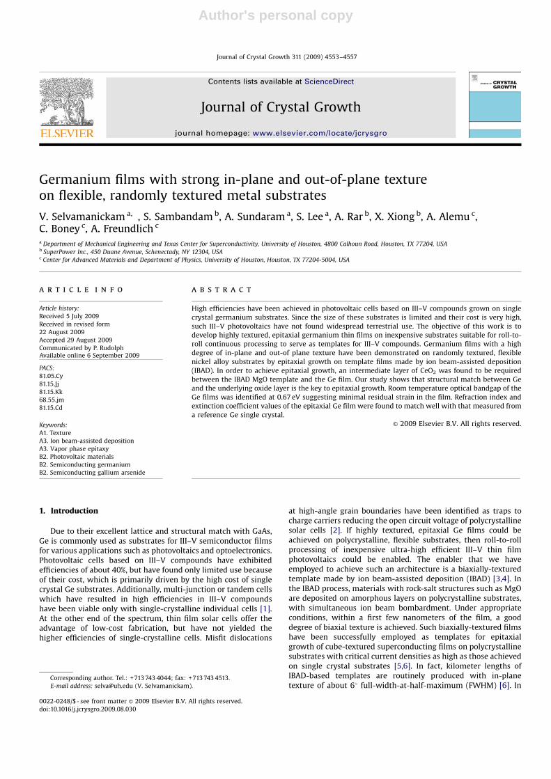
All films in the multilayer architectures prepared in this studywere grown in reel-to-reel thin film deposition systems. Fig. 1 is aschematic of the architecture that was developed in this work.Hastelloy C-276 substrates, 12 mm in width and 50mm inthickness were electropolished to a surface roughness betterthan 1 nm as measured by atomic force microscopy. An 80 nmthick Al2O3 film and a 7 nm thick Y2O3 film were deposited atroom temperature by reactive magnetron sputtering using metaltargets on the polished Hastelloy substrates. The alumina layerserves as a diffusion barrier to cations from the substrate thatcould otherwise poison the electrically active layers. Incomparison to other materials, only a thin layer of alumina isneeded to be an effective diffusion barrier which is desirable forhigh-throughput manufacturing. The yttria layer provides apristine surface for nucleation of the IBAD film. Biaxial texturedevelopment during IBAD of MgO occurs during the nucleationstage within the first few nanometers and hence it can becompromised by the templating effect if the IBAD film is grownon a polycrystalline surface. When grown on amorphous ornanocrystalline surfaces, any kind of the templating effect on IBADMgO is avoided. IBAD films were made by ion beam sputtering ofMgO at room temperature with simultaneous bombardment ofthe substrate with an Ar ion beam inclined at 451 to the substratenormal. A beam voltage of 900 eV and beam current of 180 mAwere used. Reflection high energy electron diffraction (RHEED)was used in situ during IBAD to confirm and qualify the texturedevelopment in the growing MgO film. Homo-epitaxial MgO,about 30–50 nm in thickness was grown on the IBAD films byreactive magnetron sputtering of Mg at a temperature of700–750 1C. X-ray diffraction (XRD) measurements on thehomo-epitaxial MgO film showed an in-plane texture of 6–71FWHM.
3. Epitaxial germanium
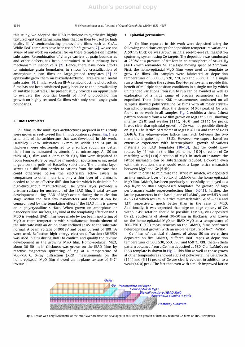
All Ge films reported in this work were deposited using thefollowing conditions except for deposition temperature variations.A 50 nm thick Ge was grown using a reel-to-reel r.f. magnetronsputtering system using Ge targets. The deposition was conductedat 250 W at a pressure of 4 mTorr in an atmosphere of Ar–4% H2
(4% H2 with remainder Ar) at a tape moving speed of 2 cm/min.First, the homo-epitaxial MgO films were used as template togrow Ge films. Six samples were fabricated at depositiontemperatures of 600, 650, 720, 770, 820 and 850 1C all in a singlerun without venting the system. Reel-to-reel systems provide thisbenefit of multiple deposition conditions in a single run by whichunintended variations from run to run can be avoided as well asexploration of a large range of process parameters can beexpedited. Theta–2theta XRD measurements conducted on allsamples showed polycrystalline Ge films with all major crystal-lographic orientations. Also, the desired (4 0 0) peak of Ge wasfound to be weak in all samples. Fig. 2 exhibits a theta–2thetapattern obtained from a Ge film grown on MgO at 600 1C showingintense (2 2 0) and weaker (111), (4 0 0) and (311) Ge peaks.It was clear that epitaxial growth of Ge was not possible directlyon MgO. The lattice parameter of MgO is 4.22 A and that of Ge is5.646 A. The edge-on-edge lattice mismatch between the twomaterials is quite high �33.8%. However, we expect, based onextensive experience with heteroepitaxial growth of variousmaterials on IBAD templates [10–13], that Ge could growrotated by 451 within the film plane, i.e. [10 0] direction of Gematching with [110] direction of MgO. In such an instance, thelattice mismatch can be substantially reduced. However, evenwith this rotation, there would exist a large lattice mismatchbetween MgO and Ge (5.4%).
Next, in order to minimize the lattice mismatch, we depositedan intermediate layer of epitaxial LaMnO3 on the homo-epitaxialMgO film. LaMnO3 has been previously successfully employed as acap layer on IBAD MgO-based templates for growth of highperformance oxide superconducting films [5,6,11]. Further, thelattice parameters in the basal plane of LaMnO3 are a=5.53 A andb=5.71 A which results in lattice mismatch with Ge of �2.1% and1.1% respectively, much better than in the case of MgO.Additionally, it was expected that edge-on-edge epitaxy of Ge,without 451 rotation should be possible. LaMnO3 was depositedby r.f. sputtering of about 30–50 nm in thickness was grownon the homo-epitaxial MgO on IBAD MgO at a temperature of700–750 1C. XRD measurements on the LaMnO3 films confirmedheteroepitaxial growth with an in-plane texture of 6–71 FWHM.
Ge films of identical thickness of about 50 nm were thendeposited on five LaMnO3 buffered IBAD tapes at depositiontemperatures of 500, 530, 550, 580, and 650 1C. XRD theta–2thetapattern obtained from a Ge film deposited at 580 1C on LaMnO3 onIBAD template is shown in Fig. 2. This film as well as those grownat other temperatures showed signs of polycrystalline Ge growth.(111) and (3 11) peaks of Ge are clearly evident in addition to aweak (4 0 0) peak. The fact that even with a much improved lattice
Fig. 1. (color web only) Schematic of the multilayer architecture developed in this work on growth of biaxially-textured Ge films on IBAD templates.
V. Selvamanickam et al. / Journal of Crystal Growth 311 (2009) 4553–45574554
Author's personal copyARTICLE IN PRESS
match, Ge did not grow epitaxially on LaMnO3 indicated thatthere should be other factors key for epitaxial growth of Ge usingIBAD templates such as structural and chemical incompatibilities.Chemical incompatibility could be due to the formation of anintermediate phase between LaMnO3 and Ge although no suchinformation has been found in the literature. We have successfullygrown non-oxides such as Ni epitaxially on LaMnO3 as well as onMgO using IBAD templates and it is not obvious why there wouldbe a chemical compatibility issue in the growth of Ge on LaMnO3
or on MgO. Structural incompatibility could be due to the lack ofmatch of the atomic locations of the basal plane of Ge andLaMnO3. Ge has a diamond structure with atoms in the fourtetrahedral hole locations, projections of which on the basal planeare at 1
4 ;14 ;0;
14 ;
34 ;0;
34 ;
14 ;0 and 3
4 ;34;0. LaMnO3 and MgO possess a
perovskite structure and rock-salt structure respectively with noatoms in the tetrahedral holes and hence do not have a goodstructural match with Ge.
We then focused specifically on the issue of structuralcompatibility between Ge and the underlying oxide layer. In thisregards, we investigated an alternate layer, CeO2, between Ge andIBAD MgO. The lattice parameter of CeO2 is 5.41 A which results ina high mismatch of �4.5% with Ge, almost as high as thatbetween MgO and Ge (considering 451 rotation of Ge lattice onMgO). We still chose CeO2 because of its better structural matchwith Ge. CeO2 has a fluorite structure with atoms in the eighttetrahedral hole locations, projections of which on the basal planeare at 1
4 ;14 ;0;
14 ;
34 ;0;
34 ;
14 ;0 and 3
4 ;34;0 which match perfectly with
the atomic locations of Ge. A meter-long CeO2 film was depositedon LaMnO3 on homo-epitaxial MgO on IBAD template in the samereel-to-reel magnetron sputtering system using conditions of300 W, 820 1C, 4 mTorr, in an atmosphere of Ar–O2 and at a tapespeed of 1.4 cm/min. XRD measurements confirmed epitaxialgrowth of CeO2.
Ge films were then deposited on six CeO2 buffered IBAD tapesat deposition temperatures of 500, 550, 580, 600, 640, 670 and720 1C. XRD theta–2theta pattern obtained from a Ge filmdeposited at 600 1C on CeO2 on IBAD template is shown inFig. 2. The presence of an intense single orientation of CeO2 (2 0 0)is obvious in the figure. Also, a strong Ge (4 0 0) orientation isseen, much stronger than the (4 0 0) peaks observed in Ge films
grown directly on MgO and LaMnO3. No evidence of (111) orother peaks of Ge is present indicating the preferential out-of-plane texture of (4 0 0) in the Ge film. The insets in Fig. 2 show theclear absence of (111) and (311) peaks of Ge compared with thefilms grown on MgO and LaMnO3.
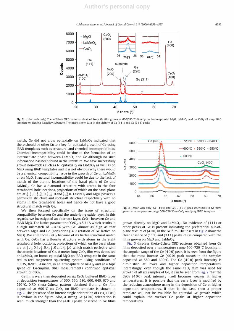
Fig. 3 displays theta–2theta XRD patterns obtained from Gefilms deposited over a temperature range 500–720 1C focusing inthe angular range of the Ge (4 0 0) peak. It is seen from the figurethat the most intense Ge (4 0 0) peak occurs in the samplesdeposited at 580 and 600 1C. The Ge (4 0 0) peak intensity isdiminished at lower and higher deposition temperatures.Interestingly, even though the same CeO2 film was used forgrowth of all six samples of Ge, it can be seen from Fig. 2 that theCeO2 (4 0 0) peak intensity itself becomes weaker at highertemperatures. It is possible that the ceria layer is modified bythe reducing atmosphere using in the deposition of Ge at higherdeposition temperatures. If that is the case, then a propertemplate will not be available for epitaxial Ge growth whichcould explain the weaker Ge peaks at higher depositiontemperatures.
0
1000
2000
3000
4000
5000
6000
7000
8000
20 30 40 50 60 70
Cou
nts
2 theta (°)
MgO
LaMnO3
CeO2
CeO2(400)
Ge(400)
CeO2(200)
LaMnO3(100)
MgO(200)
Ge (111)
Ge (311)
substrateGe
(220)
26 282 (°) 53 542 (°)
Fig. 2. (color web only) Theta–2theta XRD patterns obtained from Ge film grown at 600/580 1C directly on homo-epitaxial MgO, LaMnO3 and on CeO2 all atop IBAD
template on flexible hastelloy substrate. The insets show data in the vicinity of Ge (111) and Ge (3 11) peaks.
0
1000
2000
3000
4000
5000
6000
64
Cou
nts
2 theta (°)
720°C 670°C 640°C
600°C 580°C 550°C
500°C
CeO2 (400)
Ge (400)
65 66 67 68 69 70
Fig. 3. (color web only) Ge (4 0 0) and CeO2 (4 0 0) peak intensities in Ge films
grown at a temperature range 500–720 1C on CeO2 overlying IBAD template.
V. Selvamanickam et al. / Journal of Crystal Growth 311 (2009) 4553–4557 4555
Author's personal copyARTICLE IN PRESS
The in-plane texture of Ge was measured by XRD (111)polefigure measurements of Ge and data are shown in Fig. 4.A clear four-fold symmetry is shown in the figure without thepresence of other orientations. This result clearly demonstratesstrong biaxial texture achieved in Ge epitaxially grown on CeO2 onIBAD MgO template on metal substrate. The spread in the in-planetexture of Ge is calculated to be 6.61 FWHM which is comparableto that of the underlying IBAD MgO template. Based on ourwork on superconducting oxide films on IBAD templates, weexpect that this texture can be sharpened with growth of thickerheteroepitaxial layers.
High-resolution X-ray diffraction data were obtained from the(0 0 4) peak of Ge film and data is shown in Fig. 5. The peak isfound to be sharp at 2800 arcsec indicating the strong texture andcrystallinity of the film. The width of the peak indicates a defectdensity in the range 108–109 cm�2 which needs to be improvedfor device quality III–V semiconductor growth.
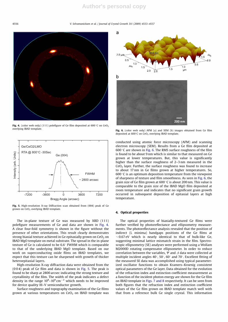
Surface roughness and topography examination of the Ge filmsgrown at various temperatures on CeO2 on IBAD template was
conducted using atomic force microscopy (AFM) and scanningelectron microscopy (SEM). Results from a Ge film deposited at600 1C are shown in Fig. 6. The RMS surface roughness of the filmis found to be about 9 nm which is similar to that measured on Gegrown at lower temperatures. But, this value is significantlyhigher than the surface roughness of 2–3 nm measured in theCeO2 layer. Further, the surface roughness was found to increaseto about 17 nm in Ge films grown at higher temperatures. So,600 1C is an optimum deposition temperature from the viewpointof sharpness of texture and film smoothness. As seen in Fig. 6, thegrain size of Ge film grown at 600 1C is about 200 nm. This value iscomparable to the grain size of the IBAD MgO film deposited atroom temperature and indicates that no significant grain growthoccurred in subsequent deposition of epitaxial layers at hightemperature.
4. Optical properties
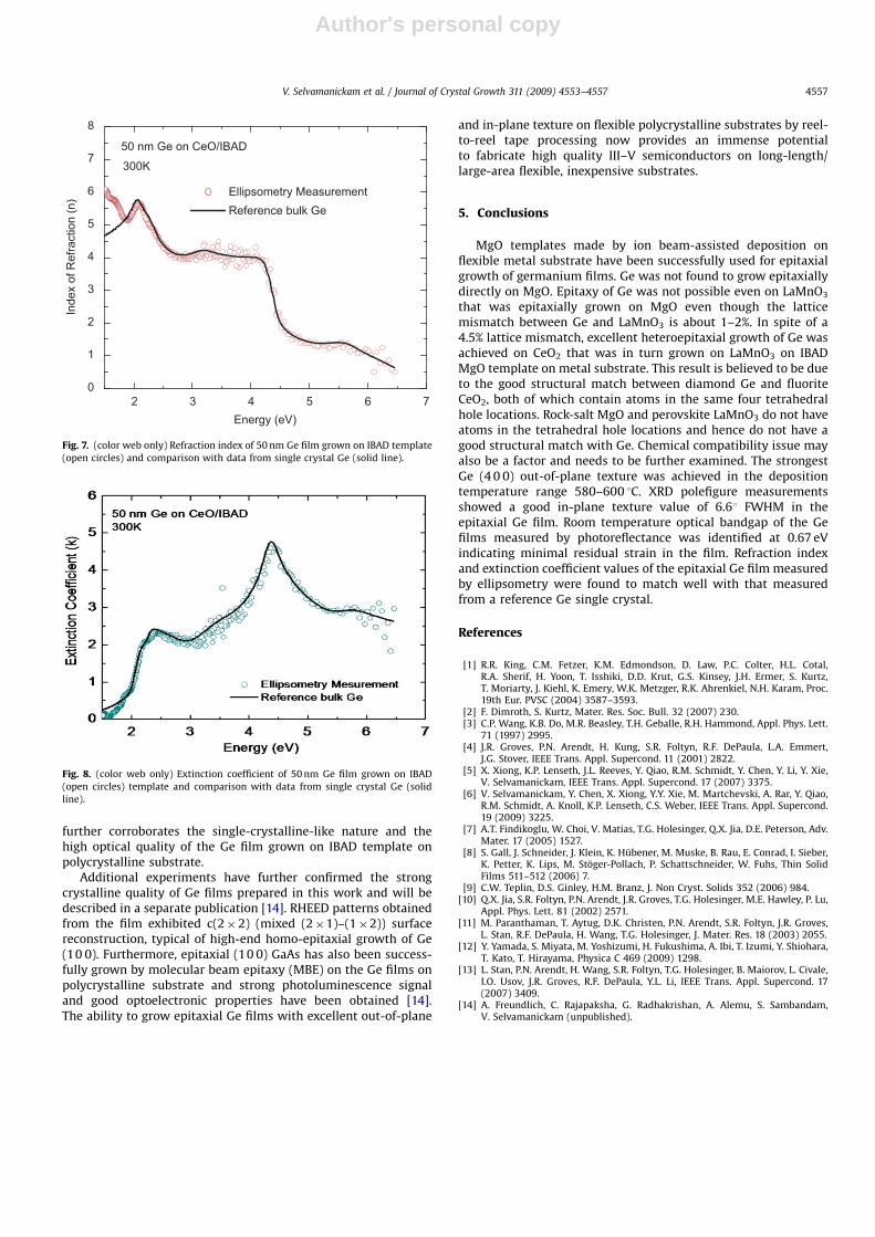
The optical properties of biaxially-textured Ge films werefurther verified by photoreflectance and ellipsometry measure-ments. The photoreflectance analysis revealed that the position ofindirect (L minima) bandgaps positions of the Ge films at�0.67 eV which is nearly identical to that of bulk-like Ge,suggesting minimal lattice mismatch strain in the film. Spectro-scopic ellipsometry (SE) analyses were performed using a WollamM2000D rotating compensator ellipsometer. In order to reducecorrelation between the variables, C and D data were collected atmultiple incident angles 401, 501, 601 and 701. Excellent fitting ofthe measured SE data was accomplished using typical parameter-ized oscillator functions to obtain Kramers–Kroenig consistentoptical parameters of the Ge layer. Data obtained for the evolutionof the refraction index and extinction coefficient measurement asa function of the incident photon energy are shown for the Ge filmon IBAD template in Figs. 7 and 8 respectively. It can be seen fromboth figures that the refraction index and extinction coefficientvalues of the Ge film grown on IBAD template match well withthat from a reference bulk Ge single crystal. This information
Fig. 4. (color web only) (111) polefigure of Ge film deposited at 600 1C on CeO2
overlying IBAD template.
Inte
nsity
(arb
. Uni
ts) RTA @ 800°C -30Sec
Ge (004)
FWHM
~ 2800 arcsec
Ge/CeO2/LMO
-7200Bragg Angle (arcsec)
-3600 0 3600 7200
Fig. 5. High-resolution X-ray Diffraction scan obtained from (004) peak of Ge
grown on CeO2 overlying IBAD template.
Fig. 6. (color web only) AFM (a) and SEM (b) images obtained from Ge film
deposited at 6001C on CeO2 overlying IBAD template.
V. Selvamanickam et al. / Journal of Crystal Growth 311 (2009) 4553–45574556
Author's personal copyARTICLE IN PRESS
further corroborates the single-crystalline-like nature and thehigh optical quality of the Ge film grown on IBAD template onpolycrystalline substrate.
Additional experiments have further confirmed the strongcrystalline quality of Ge films prepared in this work and will bedescribed in a separate publication [14]. RHEED patterns obtainedfrom the film exhibited c(2�2) (mixed (2�1)–(1�2)) surfacereconstruction, typical of high-end homo-epitaxial growth of Ge(10 0). Furthermore, epitaxial (10 0) GaAs has also been success-fully grown by molecular beam epitaxy (MBE) on the Ge films onpolycrystalline substrate and strong photoluminescence signaland good optoelectronic properties have been obtained [14].The ability to grow epitaxial Ge films with excellent out-of-plane
and in-plane texture on flexible polycrystalline substrates by reel-to-reel tape processing now provides an immense potentialto fabricate high quality III–V semiconductors on long-length/large-area flexible, inexpensive substrates.
5. Conclusions
MgO templates made by ion beam-assisted deposition onflexible metal substrate have been successfully used for epitaxialgrowth of germanium films. Ge was not found to grow epitaxiallydirectly on MgO. Epitaxy of Ge was not possible even on LaMnO3
that was epitaxially grown on MgO even though the latticemismatch between Ge and LaMnO3 is about 1–2%. In spite of a4.5% lattice mismatch, excellent heteroepitaxial growth of Ge wasachieved on CeO2 that was in turn grown on LaMnO3 on IBADMgO template on metal substrate. This result is believed to be dueto the good structural match between diamond Ge and fluoriteCeO2, both of which contain atoms in the same four tetrahedralhole locations. Rock-salt MgO and perovskite LaMnO3 do not haveatoms in the tetrahedral hole locations and hence do not have agood structural match with Ge. Chemical compatibility issue mayalso be a factor and needs to be further examined. The strongestGe (4 0 0) out-of-plane texture was achieved in the depositiontemperature range 580–600 1C. XRD polefigure measurementsshowed a good in-plane texture value of 6.61 FWHM in theepitaxial Ge film. Room temperature optical bandgap of the Gefilms measured by photoreflectance was identified at 0.67 eVindicating minimal residual strain in the film. Refraction indexand extinction coefficient values of the epitaxial Ge film measuredby ellipsometry were found to match well with that measuredfrom a reference Ge single crystal.
References
[1] R.R. King, C.M. Fetzer, K.M. Edmondson, D. Law, P.C. Colter, H.L. Cotal,R.A. Sherif, H. Yoon, T. Isshiki, D.D. Krut, G.S. Kinsey, J.H. Ermer, S. Kurtz,T. Moriarty, J. Kiehl, K. Emery, W.K. Metzger, R.K. Ahrenkiel, N.H. Karam, Proc.19th Eur. PVSC (2004) 3587–3593.
[2] F. Dimroth, S. Kurtz, Mater. Res. Soc. Bull. 32 (2007) 230.[3] C.P. Wang, K.B. Do, M.R. Beasley, T.H. Geballe, R.H. Hammond, Appl. Phys. Lett.
71 (1997) 2995.[4] J.R. Groves, P.N. Arendt, H. Kung, S.R. Foltyn, R.F. DePaula, L.A. Emmert,
J.G. Stover, IEEE Trans. Appl. Supercond. 11 (2001) 2822.[5] X. Xiong, K.P. Lenseth, J.L. Reeves, Y. Qiao, R.M. Schmidt, Y. Chen, Y. Li, Y. Xie,
V. Selvamanickam, IEEE Trans. Appl. Supercond. 17 (2007) 3375.[6] V. Selvamanickam, Y. Chen, X. Xiong, Y.Y. Xie, M. Martchevski, A. Rar, Y. Qiao,
R.M. Schmidt, A. Knoll, K.P. Lenseth, C.S. Weber, IEEE Trans. Appl. Supercond.19 (2009) 3225.
[7] A.T. Findikoglu, W. Choi, V. Matias, T.G. Holesinger, Q.X. Jia, D.E. Peterson, Adv.Mater. 17 (2005) 1527.
[8] S. Gall, J. Schneider, J. Klein, K. Hubener, M. Muske, B. Rau, E. Conrad, I. Sieber,K. Petter, K. Lips, M. Stoger-Pollach, P. Schattschneider, W. Fuhs, Thin SolidFilms 511–512 (2006) 7.
[9] C.W. Teplin, D.S. Ginley, H.M. Branz, J. Non Cryst. Solids 352 (2006) 984.[10] Q.X. Jia, S.R. Foltyn, P.N. Arendt, J.R. Groves, T.G. Holesinger, M.E. Hawley, P. Lu,
Appl. Phys. Lett. 81 (2002) 2571.[11] M. Paranthaman, T. Aytug, D.K. Christen, P.N. Arendt, S.R. Foltyn, J.R. Groves,
L. Stan, R.F. DePaula, H. Wang, T.G. Holesinger, J. Mater. Res. 18 (2003) 2055.[12] Y. Yamada, S. Miyata, M. Yoshizumi, H. Fukushima, A. Ibi, T. Izumi, Y. Shiohara,
T. Kato, T. Hirayama, Physica C 469 (2009) 1298.[13] L. Stan, P.N. Arendt, H. Wang, S.R. Foltyn, T.G. Holesinger, B. Maiorov, L. Civale,
I.O. Usov, J.R. Groves, R.F. DePaula, Y.L. Li, IEEE Trans. Appl. Supercond. 17(2007) 3409.
[14] A. Freundlich, C. Rajapaksha, G. Radhakrishan, A. Alemu, S. Sambandam,V. Selvamanickam (unpublished).
20
1
2
3
4
5
6
7
8
50 nm Ge on CeO/IBAD
300K
Inde
x of
Ref
ract
ion
(n)
Energy (eV)
Ellipsometry Measurement Reference bulk Ge
3 4 5 6 7
Fig. 7. (color web only) Refraction index of 50 nm Ge film grown on IBAD template
(open circles) and comparison with data from single crystal Ge (solid line).
Fig. 8. (color web only) Extinction coefficient of 50 nm Ge film grown on IBAD
(open circles) template and comparison with data from single crystal Ge (solid
line).
V. Selvamanickam et al. / Journal of Crystal Growth 311 (2009) 4553–4557 4557