Embed Size (px)
Citation preview
This article appeared in a journal published by Elsevier. The attachedcopy is furnished to the author for internal non-commercial researchand education use, including for instruction at the authors institution
and sharing with colleagues.
Other uses, including reproduction and distribution, or selling orlicensing copies, or posting to personal, institutional or third party
websites are prohibited.
In most cases authors are permitted to post their version of thearticle (e.g. in Word or Tex form) to their personal website orinstitutional repository. Authors requiring further information
regarding Elsevier’s archiving and manuscript policies areencouraged to visit:
http://www.elsevier.com/copyright
Author's personal copy
Synthetic Metals 161 (2011) 426–430
Contents lists available at ScienceDirect
Synthetic Metals
journa l homepage: www.e lsev ier .com/ locate /synmet
Solution-processed small molecular electron transport layer for multilayerpolymer light-emitting diodes
Zong-You Liub, Shin-Rong Tsenga, Yu-Chiang Chaoa, Chun-Yu Chena, Hsin-Fei Menga,∗,Sheng-Fu Horngc, Yu-Hsun Wud, Su-Hua Chend
a Institute of Physics, National Chiao Tung University, Hsinchu 300, Taiwan, ROCb Department of Electrophysics, National Chiao Tung University, Hsinchu 300, Taiwan, ROCc Department of Electrical Engineering, National Tsing Hua University, Hsinchu 300, Taiwan, ROCd Department of Materials Science and Engineering, National Dong Hwa University, Hualien, Taiwan, ROC
a r t i c l e i n f o
Article history:Received 27 July 2010Received in revised form15 December 2010Accepted 16 December 2010Available online 15 January 2011
Keywords:Blade coatingSolution-processed electron transportlayers
a b s t r a c t
Solution-processed electron transport layers (ETL) have been fabricated by solution processand applied in multilayer polymer light-emitting diodes with tris[2-(p-tolyl)pyridine]iridium(III)blended in poly(vinylcarbazole) as the emissive layer. Three kinds of small molecular electrontransport materials,including 2,2′,2′′-(1,3,5-benzinetriyl)-tris(1-phenyl-1-H-benzimidazole) (TPBi), 3-(4-biphenyl)-4-phenyl-5-(4-tert-butylphenyl)-1,2,4-triazole (TAZ), and 4,7-diphenyl-1,10-phenanthroline(BPhen), are tested and dissolved in methanol to form electron transport layers by blade coating. Suchelectron transport layer provides efficient electron injection and electron transport ability in the devices.The efficiency of the devices with the combination of ETL and LiF/Al cathode reaches 21.5 cd/A at 10 V(4050 cd/m2). The efficiency of the devices without ETL are 3.5 cd/A (13 V) for LiF/Al cathode and 17 cd/A(7 V) for CsF/Al cathode at 1000 cd/m2. The aggregation of the solution-processed ETL can be controlledby annealing temperature to further optimize the device performance to maximal efficiency of 53 cd/A.
© 2010 Elsevier B.V. All rights reserved.
1. Introduction
Recently the development of polymer light-emitting diodes(PLED) focuses on enhancing the device efficiency and operatinglifetime by multilayer device structure [1–4]. In the multilayerPLED, electron transport layer (ETL) plays an important role whichcan provide efficient electron transport, reduce the potential barrierbetween the emission layer (EML) and the cathode, and prevent thecathode quenching effect by hole-blocking. Concerning the fabrica-tion of PLED, solution process is low-cost and is more competitivethan the high-cost thermal evaporation. Despite of some reportsabout solution-processed PLED, the dissolution problem betweenlayers still exists in common solution-processed multilayer PLED.Therefore the ETL needs to be deposited by thermal evaporation[5–8]. In addition, if there is no ETL the device needs low workfunction or unstable cathodes, like Ca, Ba, or CsF/Al. That is oneof the reasons why the lifetime of PLED is less than that of smallmolecular organic light-emitting diodes. The cathode LiF/Al, whichis commonly used in small molecular organic light-emitting diodes,is known to be more stable than the low work function cath-
∗ Corresponding author. Tel.: +886 5731955.E-mail address: [email protected] (H.-F. Meng).
odes in PLED. Up to date there is no polymer electron transportmaterials for solution-processed PLED. There is no study to applycommon small molecular electron transport materials by solutionprocess either [9]. In this report, we demonstrate the performanceof solution-processed PLED including the ETL is comparable to theone prepared by conventional vacuum deposition. All solution-processed multilayer PLED in this work is fabricated by bladecoating method [10–12]. Three common small molecular electrontransport materials, including 2,2′,2′′-(1,3,5-benzinetriyl)-tris(1-phenyl-1-H-benzimidazole) (TPBi), 3-(4-biphenyl)-4-phenyl-5-(4-tert-butylphenyl)-1,2,4-triazole (TAZ), and 4,7-diphenyl-1,10-phenanthroline (BPhen), are dissolved in methanol, and the ETL canbe formed by blade coating method. Methanol is a very weak sol-vent to the emissive layer and the dissolution problem betweenETL and EML is solved. We find that these solution-processedsmall molecular ETLs would provide efficient electron injection andtransport ability although they may have the tendency to formaggregates. The small molecular ETLs can be optimized and theaggregation can be controlled by the annealing temperature andenvironment. Some ETLs also provide hole-blocking effect withproper energy level compared with the emissive layer and enhancethe device performance. As a result, high efficiency of multilayerPLED can be achieved by applying the solution-processed smallmolecular ETL and LiF/Al cathode.
0379-6779/$ – see front matter © 2010 Elsevier B.V. All rights reserved.doi:10.1016/j.synthmet.2010.12.021
Author's personal copy
Z.-Y. Liu et al. / Synthetic Metals 161 (2011) 426–430 427
PVK
2.3eV
5.5eV
TPD
5.5eV
2.4eV
Ir(mppy)3
2.4eV
6.2eV
PBD
2.7eV
6.7eV
TPBi
2.8eV
6.4eV
TAZ
3.0eV
6.4eV
2.2eV
5.8eV
BPhen
EML ETL
5.2eV
TFB
2.3eV
5.3eV
EML
ETL
LiF/Al
3.0eV
PEDOT:PSS
(a)
(b)
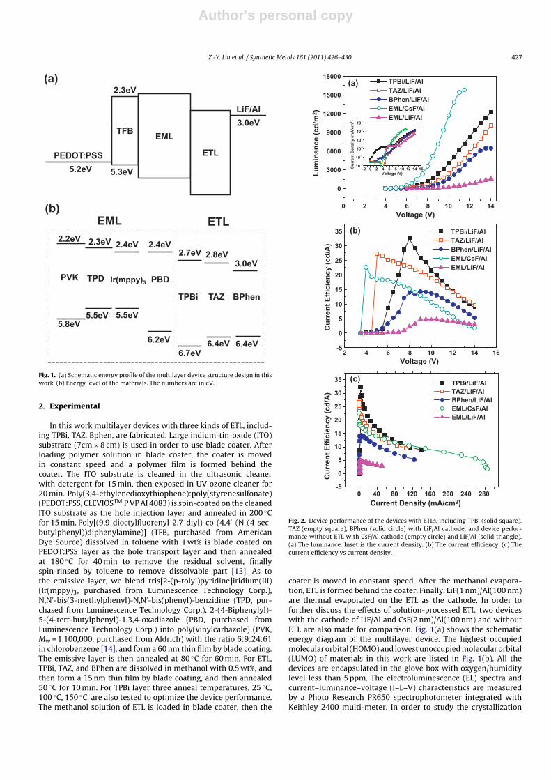
Fig. 1. (a) Schematic energy profile of the multilayer device structure design in thiswork. (b) Energy level of the materials. The numbers are in eV.
2. Experimental
In this work multilayer devices with three kinds of ETL, includ-ing TPBi, TAZ, Bphen, are fabricated. Large indium-tin-oxide (ITO)substrate (7cm × 8 cm) is used in order to use blade coater. Afterloading polymer solution in blade coater, the coater is movedin constant speed and a polymer film is formed behind thecoater. The ITO substrate is cleaned in the ultrasonic cleanerwith detergent for 15 min, then exposed in UV ozone cleaner for20 min. Poly(3,4-ethylenedioxythiophene):poly(styrenesulfonate)(PEDOT:PSS, CLEVIOSTM P VP AI 4083) is spin-coated on the cleanedITO substrate as the hole injection layer and annealed in 200 ◦Cfor 15 min. Poly[(9,9-dioctylfluorenyl-2,7-diyl)-co-(4,4′-(N-(4-sec-butylphenyl))diphenylamine)] (TFB, purchased from AmericanDye Source) dissolved in toluene with 1 wt% is blade coated onPEDOT:PSS layer as the hole transport layer and then annealedat 180 ◦C for 40 min to remove the residual solvent, finallyspin-rinsed by toluene to remove dissolvable part [13]. As tothe emissive layer, we blend tris[2-(p-tolyl)pyridine]iridium(III)(Ir(mppy)3, purchased from Luminescence Technology Corp.),N,N′-bis(3-methylphenyl)-N,N′-bis(phenyl)-benzidine (TPD, pur-chased from Luminescence Technology Corp.), 2-(4-Biphenylyl)-5-(4-tert-butylphenyl)-1,3,4-oxadiazole (PBD, purchased fromLuminescence Technology Corp.) into poly(vinylcarbazole) (PVK,Mw = 1,100,000, purchased from Aldrich) with the ratio 6:9:24:61in chlorobenzene [14], and form a 60 nm thin film by blade coating.The emissive layer is then annealed at 80 ◦C for 60 min. For ETL,TPBi, TAZ, and BPhen are dissolved in methanol with 0.5 wt%, andthen form a 15 nm thin film by blade coating, and then annealed50 ◦C for 10 min. For TPBi layer three anneal temperatures, 25 ◦C,100 ◦C, 150 ◦C, are also tested to optimize the device performance.The methanol solution of ETL is loaded in blade coater, then the
14121086420
0
3000
6000
9000
12000
15000
18000 TPBi/LiF/Al TAZ/LiF/Al BPhen/LiF/Al EML/CsF/Al EML/LiF/Al
Lu
min
ance
(cd
/m2 )
Voltage (V)
161412108642-5
0
5
10
15
20
25
30
35 TPBi/LiF/AlTAZ/LiF/AlBPhen/LiF/AlEML/CsF/AlEML/LiF/Al
Cu
rren
t E
ffic
ien
cy (
cd/A
)
Voltage (V)
(a)
(b)
28024020016012080400-5
0
5
10
15
20
25
30
35 TPBi/LiF/AlTAZ/LiF/AlBPhen/LiF/AlEML/CsF/AlEML/LiF/Al
Cu
rren
t E
ffic
ien
cy (
cd/A
)
Current Density (mA/cm2)
(c)
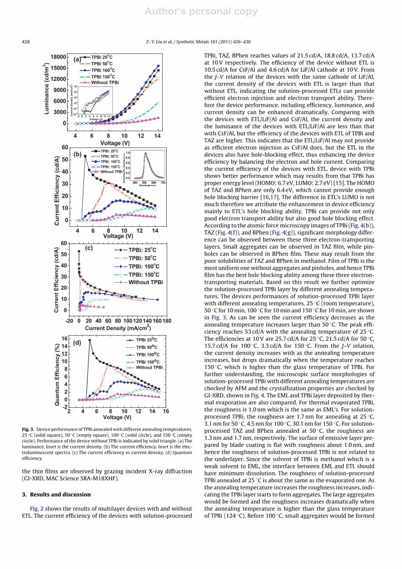
Fig. 2. Device performance of the devices with ETLs, including TPBi (solid square),TAZ (empty square), BPhen (solid circle) with LiF/Al cathode, and device perfor-mance without ETL with CsF/Al cathode (empty circle) and LiF/Al (solid triangle).(a) The luminance. Inset is the current density. (b) The current efficiency. (c) Thecurrent efficiency vs current density.
coater is moved in constant speed. After the methanol evapora-tion, ETL is formed behind the coater. Finally, LiF(1 nm)/Al(100 nm)are thermal evaporated on the ETL as the cathode. In order tofurther discuss the effects of solution-processed ETL, two deviceswith the cathode of LiF/Al and CsF(2 nm)/Al(100 nm) and withoutETL are also made for comparison. Fig. 1(a) shows the schematicenergy diagram of the multilayer device. The highest occupiedmolecular orbital (HOMO) and lowest unoccupied molecular orbital(LUMO) of materials in this work are listed in Fig. 1(b). All thedevices are encapsulated in the glove box with oxygen/humiditylevel less than 5 ppm. The electroluminescence (EL) spectra andcurrent–luminance–voltage (I–L–V) characteristics are measuredby a Photo Research PR650 spectrophotometer integrated withKeithley 2400 multi-meter. In order to study the crystallization
Author's personal copy
428 Z.-Y. Liu et al. / Synthetic Metals 161 (2011) 426–430
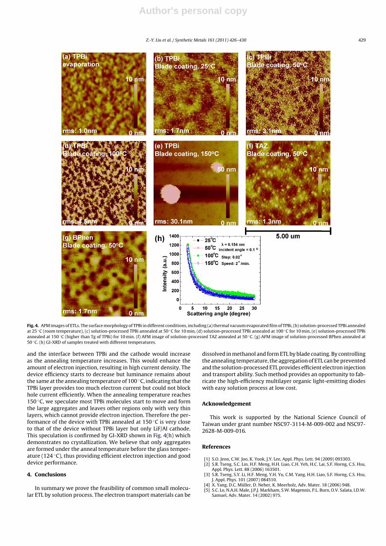
Fig. 3. Device performance of TPBi annealed with different annealing temperatures,25 ◦C (solid square), 50 ◦C (empty square), 100 ◦C (solid circle), and 150 ◦C (emptycircle). Performance of the device without TPBi is indicated by solid triangle. (a) Theluminance. Inset is the current density. (b) The current efficiency. Inset is the elec-troluminescent spectra. (c) The current efficiency vs current density. (d) Quantumefficiency.
the thin films are observed by grazing incident X-ray diffraction(GI-XRD, MAC Science SRA-M18XHF).
3. Results and discussion
Fig. 2 shows the results of multilayer devices with and withoutETL. The current efficiency of the devices with solution-processed
TPBi, TAZ, BPhen reaches values of 21.5 cd/A, 18.8 cd/A, 13.7 cd/Aat 10 V respectively. The efficiency of the device without ETL is10.5 cd/A for CsF/Al and 4.6 cd/A for LiF/Al cathode at 10 V. Fromthe J–V relation of the devices with the same cathode of LiF/Al,the current density of the devices with ETL is larger than thatwithout ETL, indicating the solution-processed ETLs can provideefficient electron injection and electron transport ability. There-fore the device performance, including efficiency, luminance, andcurrent density can be enhanced dramatically. Comparing withthe devices with ETL/LiF/Al and CsF/Al, the current density andthe luminance of the devices with ETL/LiF/Al are less than thatwith CsF/Al, but the efficiency of the devices with ETL of TPBi andTAZ are higher. This indicates that the ETL/LiF/Al may not provideas efficient electron injection as CsF/Al does, but the ETL in thedevices also have hole-blocking effect, thus enhancing the deviceefficiency by balancing the electron and hole current. Comparingthe current efficiency of the devices with ETL, device with TPBishows better performance which may results from that TPBi hasproper energy level (HOMO: 6.7 eV, LUMO: 2.7 eV) [15]. The HOMOof TAZ and BPhen are only 6.4 eV, which cannot provide enoughhole blocking barrier [16,17]. The difference in ETL’s LUMO is notmuch therefore we attribute the enhancement in device efficiencymainly to ETL’s hole blocking ability. TPBi can provide not onlygood electron transport ability but also good hole blocking effect.According to the atomic force microscopy images of TPBi (Fig. 4(b)),TAZ (Fig. 4(f)), and BPhen (Fig. 4(g)), significant morphology differ-ence can be observed between these three electron-transportinglayers. Small aggregates can be observed in TAZ film, while pin-holes can be observed in BPhen film. These may result from thepoor solubilities of TAZ and BPhen in methanol. Film of TPBi is themost uniform one without aggregates and pinholes, and hence TPBifilm has the best hole blocking ability among these three electron-transporting materials. Based on this result we further optimizethe solution-processed TPBi layer by different annealing tempera-tures. The devices performances of solution-processed TPBi layerwith different annealing temperatures, 25 ◦C (room temperature),50 ◦C for 10 min, 100 ◦C for 10 min and 150 ◦C for 10 min, are shownin Fig. 3. As can be seen the current efficiency decreases as theannealing temperature increases larger than 50 ◦C. The peak effi-ciency reaches 53 cd/A with the annealing temperature of 25 ◦C.The efficiencies at 10 V are 25.7 cd/A for 25 ◦C, 21.5 cd/A for 50 ◦C,15.7 cd/A for 100 ◦C, 3.3 cd/A for 150 ◦C. From the J–V relation,the current density increases with as the annealing temperatureincreases, but drops dramatically when the temperature reaches150 ◦C, which is higher than the glass temperature of TPBi. Forfurther understanding, the microscopic surface morphologies ofsolution-processed TPBi with different annealing temperatures arechecked by AFM and the crystallization properties are checked byGI-XRD, shown in Fig. 4. The EML and TPBi layer deposited by ther-mal evaporation are also compared. For thermal evaporated TPBi,the roughness is 1.0 nm which is the same as EML’s. For solution-processed TPBi, the roughness are 1.7 nm for annealing at 25 ◦C,3.1 nm for 50 ◦C, 4.5 nm for 100 ◦C, 30.1 nm for 150 ◦C. For solution-processed TAZ and BPhen annealed at 50 ◦C, the roughness are1.3 nm and 1.7 nm, respectively. The surface of emissive layer pre-pared by blade coating is flat with roughness about 1.0 nm, andhence the roughness of solution-processed TPBi is not related tothe underlayer. Since the solvent of TPBi is methanol which is aweak solvent to EML, the interface between EML and ETL shouldhave minimum dissolution. The roughness of solution-processedTPBi annealed at 25 ◦C is about the same as the evaporated one. Asthe annealing temperature increases the roughness increases, indi-cating the TPBi layer starts to form aggregates. The large aggregateswould be formed and the roughness increases dramatically whenthe annealing temperature is higher than the glass temperatureof TPBi (124 ◦C). Before 100 ◦C, small aggregates would be formed
Author's personal copy
Z.-Y. Liu et al. / Synthetic Metals 161 (2011) 426–430 429
Fig. 4. AFM images of ETLs. The surface morphology of TPBi in different conditions, including (a) thermal vacuum evaporated film of TPBi, (b) solution-processed TPBi annealedat 25 ◦C (room temperature), (c) solution-processed TPBi annealed at 50 ◦C for 10 min, (d) solution-processed TPBi annealed at 100 ◦C for 10 min, (e) solution-processed TPBiannealed at 150 ◦C (higher than Tg of TPBi) for 10 min. (f) AFM image of solution-processed TAZ annealed at 50 ◦C. (g) AFM image of solution-processed BPhen annealed at50 ◦C. (h) GI-XRD of samples treated with different temperatures.
and the interface between TPBi and the cathode would increaseas the annealing temperature increases. This would enhance theamount of electron injection, resulting in high current density. Thedevice efficiency starts to decrease but luminance remains aboutthe same at the annealing temperature of 100 ◦C, indicating that theTPBi layer provides too much electron current but could not blockhole current efficiently. When the annealing temperature reaches150 ◦C, we speculate most TPBi molecules start to move and formthe large aggregates and leaves other regions only with very thinlayers, which cannot provide electron injection. Therefore the per-formance of the device with TPBi annealed at 150 ◦C is very closeto that of the device without TPBi layer but only LiF/Al cathode.This speculation is confirmed by GI-XRD shown in Fig. 4(h) whichdemonstrates no crystallization. We believe that only aggregatesare formed under the anneal temperature before the glass temper-ature (124 ◦C), thus providing efficient electron injection and gooddevice performance.
4. Conclusions
In summary we prove the feasibility of common small molecu-lar ETL by solution process. The electron transport materials can be
dissolved in methanol and form ETL by blade coating. By controllingthe annealing temperature, the aggregation of ETL can be preventedand the solution-processed ETL provides efficient electron injectionand transport ability. Such method provides an opportunity to fab-ricate the high-efficiency multilayer organic light-emitting diodeswith easy solution process at low cost.
Acknowledgement
This work is supported by the National Science Council ofTaiwan under grant number NSC97-3114-M-009-002 and NSC97-2628-M-009-016.
References
[1] S.O. Jeon, C.W. Joo, K. Yook, J.Y. Lee, Appl. Phys. Lett. 94 (2009) 093303.[2] S.R. Tseng, S.C. Lin, H.F. Meng, H.H. Liao, C.H. Yeh, H.C. Lai, S.F. Horng, C.S. Hsu,
Appl. Phys. Lett. 88 (2006) 163501.[3] S.R. Tseng, S.Y. Li, H.F. Meng, Y.H. Yu, C.M. Yang, H.H. Liao, S.F. Horng, C.S. Hsu,
J. Appl. Phys. 101 (2007) 084510.[4] X. Yang, D.C. Müller, D. Neher, K. Meerholz, Adv. Mater. 18 (2006) 948.[5] S.C. Lo, N.A.H. Male, J.P.J. Markham, S.W. Magennis, P.L. Burn, O.V. Salata, I.D.W.
Samuel, Adv. Mater. 14 (2002) 975.

Author's personal copy
430 Z.-Y. Liu et al. / Synthetic Metals 161 (2011) 426–430
[6] J.J. Park, T.J. Park, W.S. Jeon, R. Pode, J. Jang, J.H. Kwon, E.S. Yu, M.Y. Chae, Org.Electron. 10 (2009) 189.
[7] H. Kim, Y. Byun, R.R. Das, B.K. Choi, P.S. Ahn, Appl. Phys. Lett. 91 (2007) 093512.[8] K.S. Yook, S.E. Jang, S.O. Jeon, J.Y. Lee, Adv. Mater. 22 (2010) 4479.[9] T. Earmme, E. Ahmed, S.A. Jenekhe, Adv. Mater. 22 (2010) 4744.
[10] S.R. Tseng, H.F. Meng, K.C. Lee, S.F. Horng, Appl. Phys. Lett. 93 (2008)153308.
[11] J.D. You, S.R. Tseng, H.F. Meng, F.W. Yen, I.F. Lin, S.F. Horng, Org. Electron. 10(2009) 1610.
[12] Y.H. Chang, S.R. Tseng, C.Y. Chen, H.F. Meng, E.C. Chen, S.F. Horng, C.S. Hsu, Org.Electron. 10 (2009) 741.
[13] J.S. Kim, R.H. Friend, I. Grizzi, J.H. Burroughes, Appl. Phys. Lett. 87 (2005) 023506.[14] S.A. Choulis, V.E. Choong, M.K. Mathai, F. So, Appl. Phys. Lett. 87 (2005) 113503.[15] E.B. Namdas, T.D. Anthopoulos, I.D.W. Samuel, M.J. Frampton, S.C. Lo, P.L. Burn,
Appl. Phys. Lett. 86 (2005) 161104.[16] M. Cocchi, J. Kalinowski, S. Stagni, S. Muzzioli, Appl. Phys. Lett. 94 (2009)
083306.[17] S. Liu, B. Li, L. Zhang, H. Song, H. Jiang, Appl. Phys. Lett. 97 (2010) 083304.