Embed Size (px)
Citation preview
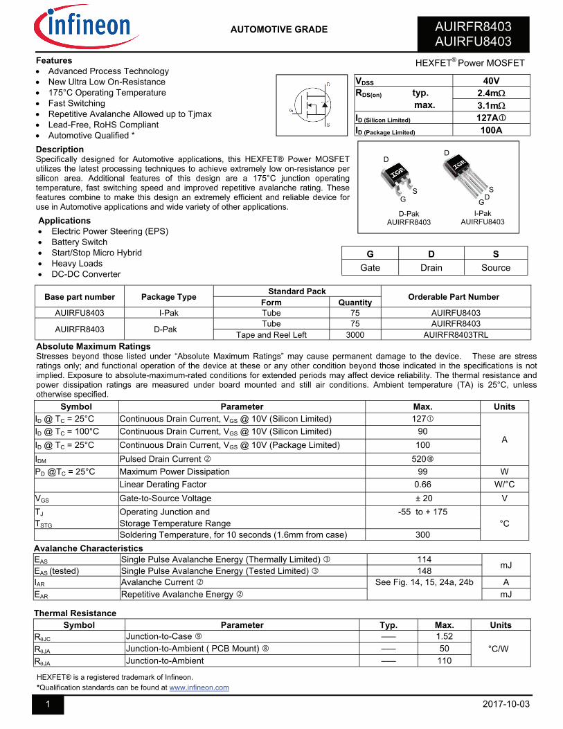
AUIRFR8403 AUIRFU8403
VDSS 40V RDS(on) typ. 2.4m
ID (Silicon Limited) 127A
max. 3.1m
ID (Package Limited) 100A
Features Advanced Process Technology New Ultra Low On-Resistance 175°C Operating Temperature Fast Switching Repetitive Avalanche Allowed up to Tjmax Lead-Free, RoHS Compliant Automotive Qualified *
Description Specifically designed for Automotive applications, this HEXFET® Power MOSFET utilizes the latest processing techniques to achieve extremely low on-resistance per silicon area. Additional features of this design are a 175°C junction operating temperature, fast switching speed and improved repetitive avalanche rating. These features combine to make this design an extremely efficient and reliable device for use in Automotive applications and wide variety of other applications.
1 2017-10-03
HEXFET® is a registered trademark of Infineon.
*Qualification standards can be found at www.infineon.com
AUTOMOTIVE GRADE
Symbol Parameter Max. Units ID @ TC = 25°C Continuous Drain Current, VGS @ 10V (Silicon Limited) 127
A ID @ TC = 100°C Continuous Drain Current, VGS @ 10V (Silicon Limited) 90
ID @ TC = 25°C Continuous Drain Current, VGS @ 10V (Package Limited) 100
IDM Pulsed Drain Current 520
PD @TC = 25°C Maximum Power Dissipation 99 W
Linear Derating Factor 0.66 W/°C
VGS Gate-to-Source Voltage ± 20 V
TJ Operating Junction and -55 to + 175
TSTG Storage Temperature Range °C
Soldering Temperature, for 10 seconds (1.6mm from case) 300
Absolute Maximum Ratings Stresses beyond those listed under “Absolute Maximum Ratings” may cause permanent damage to the device. These are stress ratings only; and functional operation of the device at these or any other condition beyond those indicated in the specifications is not implied. Exposure to absolute-maximum-rated conditions for extended periods may affect device reliability. The thermal resistance and power dissipation ratings are measured under board mounted and still air conditions. Ambient temperature (TA) is 25°C, unless otherwise specified.
Thermal Resistance Symbol Parameter Typ. Max. Units
RJC Junction-to-Case ––– 1.52
°C/W RJA Junction-to-Ambient ( PCB Mount) ––– 50
RJA Junction-to-Ambient ––– 110
D-Pak AUIRFR8403
I-Pak AUIRFU8403
Base part number Package Type Standard Pack
Form Quantity AUIRFU8403 I-Pak Tube 75 AUIRFU8403
AUIRFR8403 D-Pak Tube 75 AUIRFR8403
Tape and Reel Left 3000 AUIRFR8403TRL
Orderable Part Number
G D S
Gate Drain Source
G
S D
D
S G
D
Avalanche Characteristics EAS Single Pulse Avalanche Energy (Thermally Limited) 114 EAS (tested) Single Pulse Avalanche Energy (Tested Limited) 148 IAR Avalanche Current See Fig. 14, 15, 24a, 24b A EAR Repetitive Avalanche Energy mJ
mJ
Applications Electric Power Steering (EPS) Battery Switch Start/Stop Micro Hybrid Heavy Loads DC-DC Converter
HEXFET® Power MOSFET
AUIRFR/U8403
2 2017-10-03
Notes: Calculated continuous current based on maximum allowable junction temperature. Bond wire current limit is 100A by source bonding technology. Note that current limitations arising from heating of the device leads may occur with some lead mounting arrangements. (Refer to AN-1140) Repetitive rating; pulse width limited by max. junction temperature. (See fig. 11) Limited by TJmax , starting TJ = 25°C, L = 0.039mH, RG = 50, IAS = 76A, VGS =10V. Part not recommended for use above this value. ISD 76A, di/dt 1255A/µs, VDD V(BR)DSS, TJ 175°C. Pulse width 400µs; duty cycle 2%. Coss eff. (TR) is a fixed capacitance that gives the same charging time as Coss while VDS is rising from 0 to 80% VDSS. Coss eff. (ER) is a fixed capacitance that gives the same energy as Coss while VDS is rising from 0 to 80% VDSS. When mounted on 1" square PCB (FR-4 or G-10 Material). For recommended footprint and soldering techniques refer to application note #AN-994 Ris measured at TJ approximately 90°C. Pulse drain current is limited by source bonding technology.
Static @ TJ = 25°C (unless otherwise specified)
Parameter Min. Typ. Max. Units Conditions
V(BR)DSS Drain-to-Source Breakdown Voltage 40 ––– ––– V VGS = 0V, ID = 250µA V(BR)DSS/TJ Breakdown Voltage Temp. Coefficient ––– 0.03 ––– V/°C Reference to 25°C, ID = 5mA
RDS(on) Static Drain-to-Source On-Resistance ––– 2.4 3.1 m VGS = 10V, ID = 76A
VGS(th) Gate Threshold Voltage 2.2 3.0 3.9 V VDS = VGS, ID = 100µA
IDSS Drain-to-Source Leakage Current ––– ––– 1.0
µA VDS = 40V, VGS = 0V
––– ––– 150 VDS = 40V,VGS = 0V,TJ =125°C
IGSS Gate-to-Source Forward Leakage ––– ––– 100
nA VGS = 20V
Gate-to-Source Reverse Leakage ––– ––– -100 VGS = -20V RG Internal Gate Resistance ––– 1.5 –––
Dynamic Electrical Characteristics @ TJ = 25°C (unless otherwise specified)
gfs Forward Trans conductance 283 ––– ––– S VDS = 10V, ID = 76A Qg Total Gate Charge ––– 66 99
nC
ID = 76A Qgs Gate-to-Source Charge ––– 18 ––– VDS = 20V Qgd Gate-to-Drain Charge ––– 22 ––– VGS = 10V Qsync Total Gate Charge Sync. (Qg - Qgd) ––– 44 ––– td(on) Turn-On Delay Time ––– 10 –––
ns
VDD = 26V tr Rise Time ––– 32 ––– ID = 76A td(off) Turn-Off Delay Time ––– 31 ––– RG = 2.7tf Fall Time ––– 23 ––– VGS = 10V Ciss Input Capacitance ––– 3171 –––
pF
VGS = 0V Coss Output Capacitance ––– 477 ––– VDS = 25V Crss Reverse Transfer Capacitance ––– 331 ––– ƒ = 1.0MHz, See Fig. 5 Coss eff. (ER) Effective Output Capacitance (Energy Related) ––– 573 ––– VGS = 0V, VDS = 0V to 32V Coss eff. (TR) Effective Output Capacitance (Time Related) ––– 681 ––– VGS = 0V, VDS = 0V to 32V
Diode Characteristics
Parameter Min. Typ. Max. Units Conditions
IS Continuous Source Current
––– ––– 127 A
MOSFET symbol (Body Diode) showing the
ISM Pulsed Source Current
––– ––– 520 integral reverse
(Body Diode) p-n junction diode. VSD Diode Forward Voltage ––– 0.9 1.3 V TJ = 25°C,IS = 76A,VGS = 0V dv/dt Peak Diode Recovery dv/dt ––– 5.1 ––– V/ns TJ = 175°C,IS = 76A,VDS = 40V trr Reverse Recovery Time ––– 25 –––
ns TJ = 25°C
––– 26 ––– TJ = 125°C Qrr Reverse Recovery Charge ––– 20 –––
nC TJ = 25°C
––– 21 ––– TJ = 125°C IRRM Reverse Recovery Current ––– 1.2 ––– A TJ = 25°C
VR = 34V, IF = 76A di/dt = 100A/µs
AUIRFR/U8403
3 2017-10-03
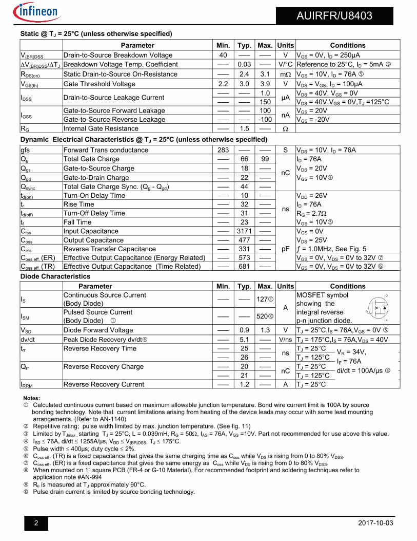
Fig. 2 Typical Output Characteristics
Fig. 3 Typical Transfer Characteristics
Fig. 1 Typical Output Characteristics
Fig 5. Typical Capacitance vs. Drain-to-Source Voltage Fig 6. Typical Gate Charge vs. Gate-to-Source Voltage
Fig. 4 Normalized On-Resistance vs. Temperature
0.1 1 10 100
VDS, Drain-to-Source Voltage (V)
0.1
1
10
100
1000
I D, D
rain
-to-
Sou
rce
Cu
rren
t (A
)VGS
TOP 15V10V7.0V6.0V5.5V5.0V4.5V
BOTTOM 4.3V
60µs PULSE WIDTHTj = 25°C
4.3V
0.1 1 10 100
VDS, Drain-to-Source Voltage (V)
1
10
100
1000
I D, D
rain
-to-
Sou
rce
Cu
rren
t (A
)
VGSTOP 15V
10V7.0V6.0V5.5V5.0V4.5V
BOTTOM 4.3V
60µs PULSE WIDTHTj = 175°C
4.3V
2 3 4 5 6 7 8
VGS, Gate-to-Source Voltage (V)
0.1
1
10
100
1000
I D, D
rain
-to-
Sou
rce
Cur
rent
(A
)
TJ = 25°C
TJ = 175°C
VDS = 10V
60µs PULSE WIDTH
-60 -20 20 60 100 140 180
TJ , Junction Temperature (°C)
0.4
0.8
1.2
1.6
2.0
RD
S(o
n) ,
Dra
in-t
o-S
ourc
e O
n R
esis
tanc
e
(
Nor
mal
ized
)
ID = 76A
VGS = 10V
0.1 1 10 100
VDS, Drain-to-Source Voltage (V)
100
1000
10000
100000
C, C
apac
itanc
e (p
F)
VGS = 0V, f = 1 MHZCiss = Cgs + Cgd, C ds SHORTED
Crss = Cgd Coss = Cds + Cgd
Coss
Crss
Ciss
0 10 20 30 40 50 60 70 80 90
QG, Total Gate Charge (nC)
0.0
2.0
4.0
6.0
8.0
10.0
12.0
14.0
VG
S, G
ate-
to-S
ourc
e V
olta
ge (
V)
VDS= 32V
VDS= 20V
ID = 76A
AUIRFR/U8403
4 2017-10-03
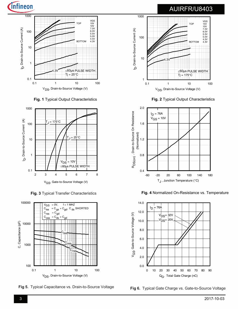
Fig 8. Maximum Safe Operating Area Fig. 7 Typical Source-to-Drain Diode Forward Voltage
Fig. 9 Maximum Drain Current vs. Case Temperature
Fig 12. Maximum Avalanche Energy vs. Drain Current Fig. 11 Typical COSS Stored Energy
0.2 0.4 0.6 0.8 1.0 1.2 1.4 1.6
VSD, Source-to-Drain Voltage (V)
0.1
1
10
100
1000I S
D, R
ever
se D
rain
Cur
rent
(A
)
TJ = 25°C
TJ = 175°C
VGS = 0V
0.1 1 10 100
VDS, Drain-to-Source Voltage (V)
0.01
0.1
1
10
100
1000
10000
I D,
Dra
in-t
o-S
ourc
e C
urre
nt (
A)
Tc = 25°CTj = 175°CSingle Pulse
1msec
10msec
OPERATION IN THIS AREA LIMITED BY RDS(on)
100µsec
DC
25 50 75 100 125 150 175
TC , Case Temperature (°C)
0
20
40
60
80
100
120
140
I D,
Dra
in C
urre
nt (
A)
Limited By Package
-60 -20 20 60 100 140 180
TJ , Temperature ( °C )
40
41
42
43
44
45
46
47
48
49
50
V(B
R)D
SS
, Dra
in-t
o-S
ourc
e B
reak
dow
n V
olta
ge (
V)
Id = 5.0mA
-5 0 5 10 15 20 25 30 35 40 45
VDS, Drain-to-Source Voltage (V)
0.0
0.1
0.1
0.2
0.2
0.3
0.3
0.4
0.4
0.5
Ene
rgy
(µJ)
25 50 75 100 125 150 175
Starting TJ , Junction Temperature (°C)
0
100
200
300
400
500
EA
S ,
Sin
gle
Pul
se A
vala
nche
Ene
rgy
(mJ) ID
TOP 13A 24ABOTTOM 76A
Fig 10. Drain-to-Source Breakdown Voltage
AUIRFR/U8403
5 2017-10-03
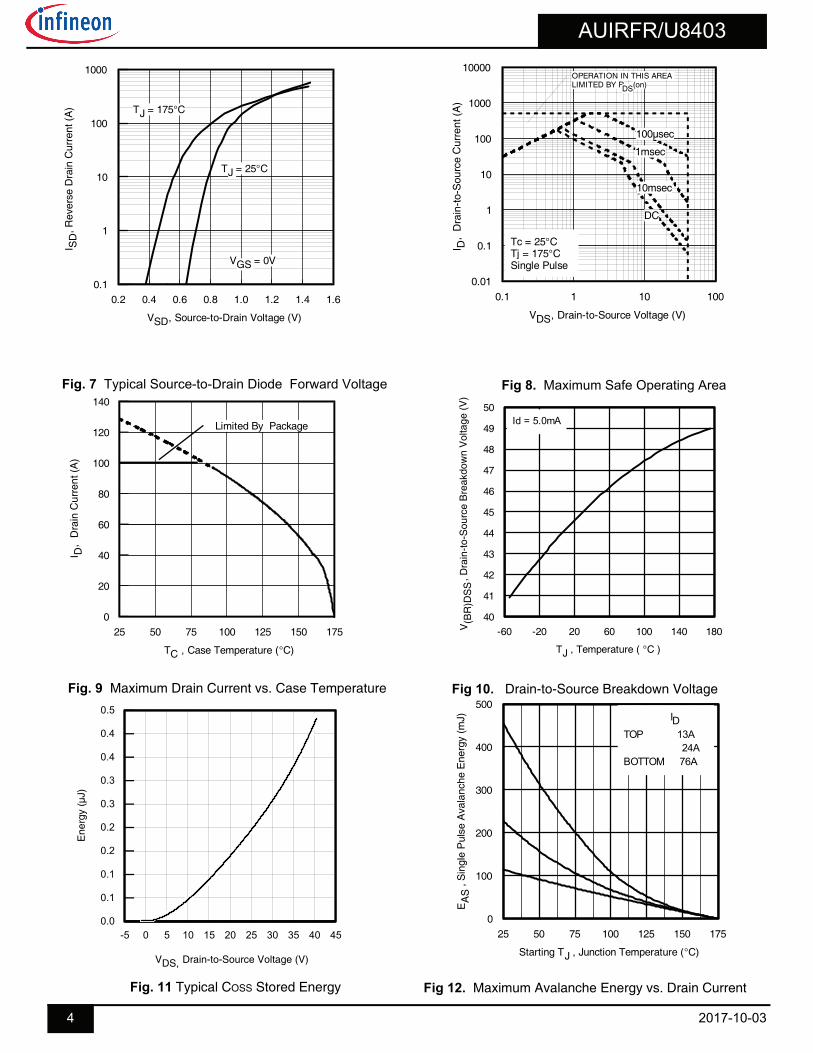
Notes on Repetitive Avalanche Curves , Figures 14, 15: (For further info, see AN-1005 at www.infineon.com) 1. Avalanche failures assumption: Purely a thermal phenomenon and failure occurs at a temperature far in excess of Tjmax. This is validated for every part type. 2. Safe operation in Avalanche is allowed as long as Tjmax is not exceeded. 3. Equation below based on circuit and waveforms shown in Figures 24a, 24b. 4. PD (ave) = Average power dissipation per single avalanche pulse. 5. BV = Rated breakdown voltage (1.3 factor accounts for voltage increase during avalanche). 6. Iav = Allowable avalanche current.
7. T = Allowable rise in junction temperature, not to exceed Tjmax (assumed as 25°C in Figure 13, 14). tav = Average time in avalanche. D = Duty cycle in avalanche = tav ·f ZthJC(D, tav) = Transient thermal resistance, see Figures 13)
PD (ave) = 1/2 ( 1.3·BV·Iav) = T/ ZthJC
Iav = 2T/ [1.3·BV·Zth]
EAS (AR) = PD (ave)·tav Fig 15. Maximum Avalanche Energy Vs. Temperature
1E-006 1E-005 0.0001 0.001 0.01 0.1
t1 , Rectangular Pulse Duration (sec)
0.001
0.01
0.1
1
10
The
rmal
Res
pons
e (
Z th
JC )
°C
/W0.20
0.10
D = 0.50
0.020.01
0.05
SINGLE PULSE( THERMAL RESPONSE ) Notes:
1. Duty Factor D = t1/t22. Peak Tj = P dm x Zthjc + Tc
1.0E-06 1.0E-05 1.0E-04 1.0E-03 1.0E-02 1.0E-01
tav (sec)
0.1
1
10
100
1000
Ava
lanc
he C
urre
nt (
A)
0.05
Duty Cycle = Single Pulse
0.10
Allowed avalanche Current vs avalanche pulsewidth, tav, assuming j = 25°C and Tstart = 150°C.
0.01
Allowed avalanche Current vs avalanche pulsewidth, tav, assuming Tj = 150°C and Tstart =25°C (Single Pulse)
Fig 13. Maximum Effective Transient Thermal Impedance, Junction-to-Case
25 50 75 100 125 150 175
Starting TJ , Junction Temperature (°C)
0
20
40
60
80
100
120
EA
R ,
Ava
lanc
he E
nerg
y (m
J)
TOP Single Pulse BOTTOM 1.0% Duty CycleID = 76A
Fig 14. Typical Avalanche Current Vs. Pulse width
AUIRFR/U8403
6 2017-10-03
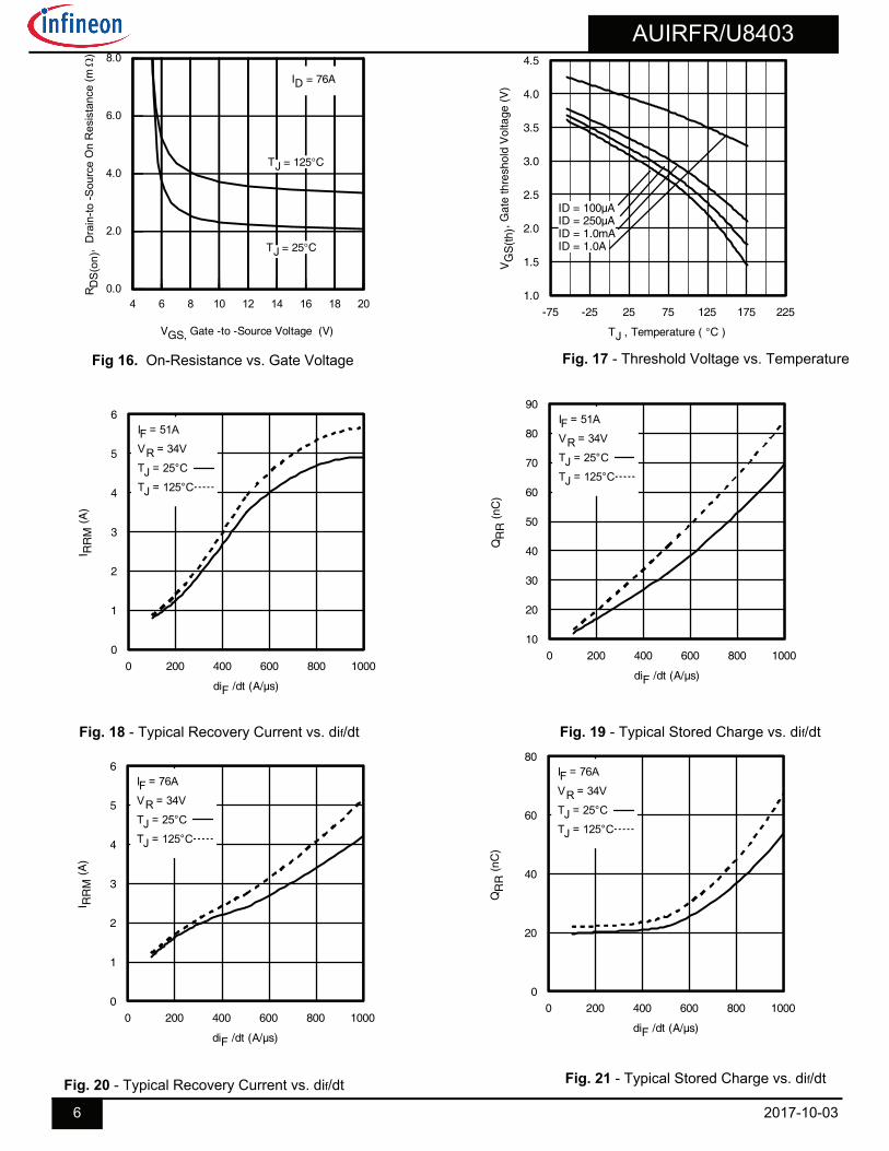
Fig 16. On-Resistance vs. Gate Voltage
Fig. 18 - Typical Recovery Current vs. dif/dt
Fig. 20 - Typical Recovery Current vs. dif/dt
Fig. 19 - Typical Stored Charge vs. dif/dt
4 6 8 10 12 14 16 18 20
VGS, Gate -to -Source Voltage (V)
0.0
2.0
4.0
6.0
8.0
RD
S(o
n),
Dra
in-t
o -S
ourc
e O
n R
esi
stan
ce (
m
)ID = 76A
TJ = 25°C
TJ = 125°C
Fig. 21 - Typical Stored Charge vs. dif/dt
-75 -25 25 75 125 175 225
TJ , Temperature ( °C )
1.0
1.5
2.0
2.5
3.0
3.5
4.0
4.5
VG
S(t
h), G
ate
thre
shol
d V
olta
ge (
V)
ID = 100µAID = 250µAID = 1.0mAID = 1.0A
Fig. 17 - Threshold Voltage vs. Temperature
0 200 400 600 800 1000
diF /dt (A/µs)
0
1
2
3
4
5
6
I RR
M (
A)
IF = 51A
VR = 34V
TJ = 25°C
TJ = 125°C
0 200 400 600 800 1000
diF /dt (A/µs)
10
20
30
40
50
60
70
80
90
QR
R (
nC)
IF = 51A
VR = 34V
TJ = 25°C
TJ = 125°C
0 200 400 600 800 1000
diF /dt (A/µs)
0
1
2
3
4
5
6
I RR
M (
A)
IF = 76A
VR = 34V
TJ = 25°C
TJ = 125°C
0 200 400 600 800 1000
diF /dt (A/µs)
0
20
40
60
80
QR
R (
nC)
IF = 76A
VR = 34V
TJ = 25°C
TJ = 125°C
AUIRFR/U8403
7 2017-10-03
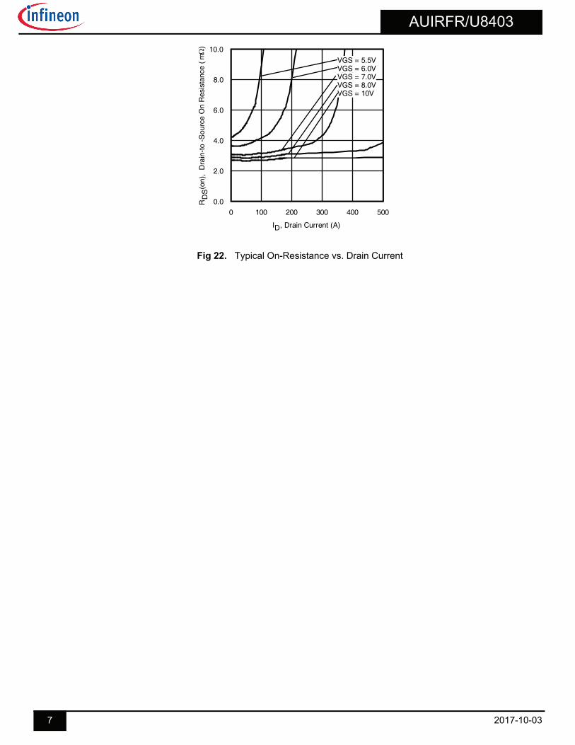
Fig 22. Typical On-Resistance vs. Drain Current
0 100 200 300 400 500
ID, Drain Current (A)
0.0
2.0
4.0
6.0
8.0
10.0
RD
S(o
n),
Dra
in-t
o -S
ourc
e O
n R
esis
tanc
e (m
)
VGS = 5.5VVGS = 6.0VVGS = 7.0VVGS = 8.0VVGS = 10V

AUIRFR/U8403
8 2017-10-03
Fig 23. Peak Diode Recovery dv/dt Test Circuit for N-Channel HEXFET® Power MOSFETs
Fig 25a. Switching Time Test Circuit Fig 25b. Switching Time Waveforms
Fig 24a. Unclamped Inductive Test Circuit
RG
IAS
0.01tp
D.U.T
LVDS
+- VDD
DRIVER
A
15V
20V
Fig 24b. Unclamped Inductive Waveforms
tp
V(BR)DSS
IAS
Fig 26b. Gate Charge Waveform
Vds
Vgs
Id
Vgs(th)
Qgs1 Qgs2 Qgd Qgodr
Fig 26a. Gate Charge Test Circuit
AUIRFR/U8403
9 2017-10-03
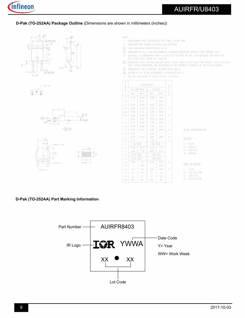
D-Pak (TO-252AA) Package Outline (Dimensions are shown in millimeters (inches))
YWWA
XX XX
Date Code
Y= Year
WW= Work Week
AUIRFR8403
Lot Code
Part Number
IR Logo
D-Pak (TO-252AA) Part Marking Information
AUIRFR/U8403
10 2017-10-03
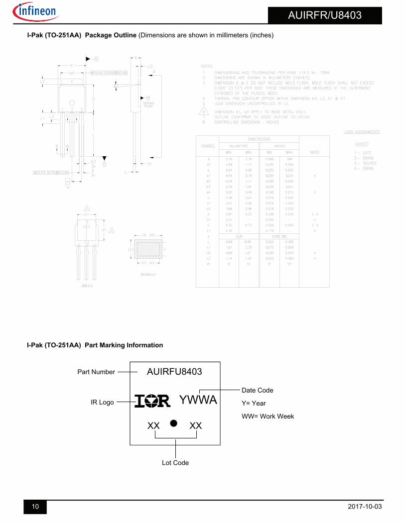
I-Pak (TO-251AA) Part Marking Information
YWWA
XX XX
Date Code
Y= Year
WW= Work Week
AUIRFU8403
Lot Code
Part Number
IR Logo
I-Pak (TO-251AA) Package Outline (Dimensions are shown in millimeters (inches)
AUIRFR/U8403
11 2017-10-03
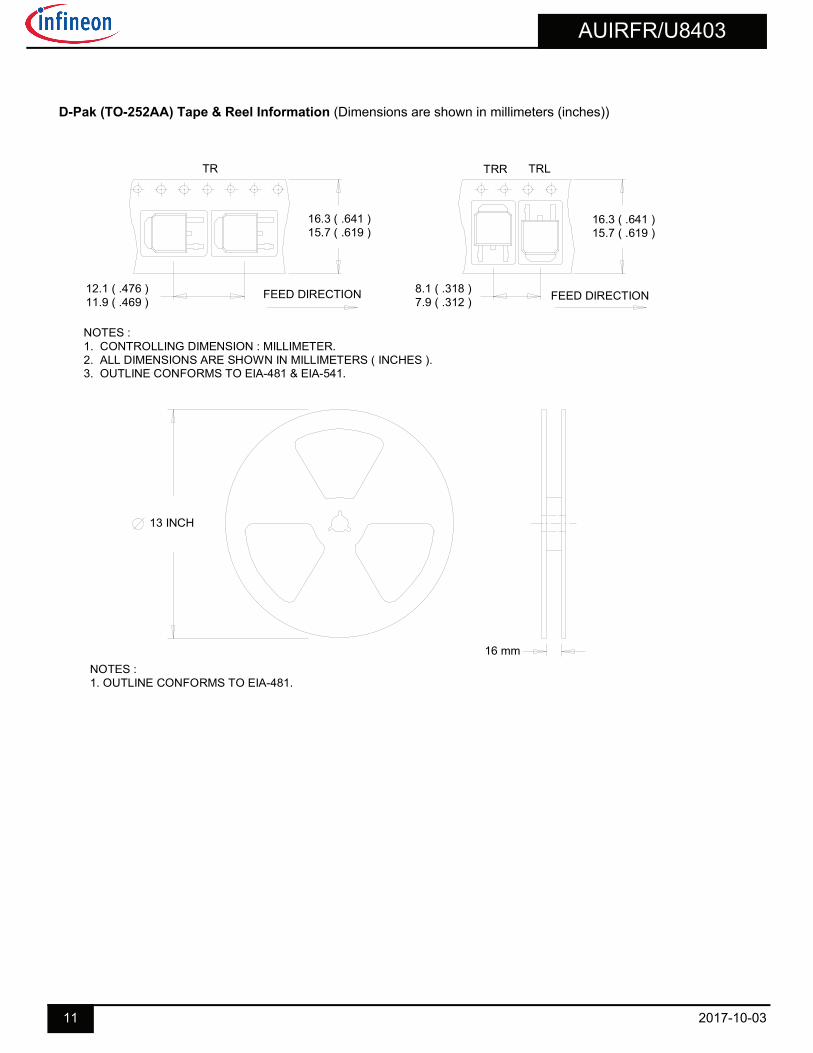
D-Pak (TO-252AA) Tape & Reel Information (Dimensions are shown in millimeters (inches))
TR
16.3 ( .641 )15.7 ( .619 )
8.1 ( .318 )7.9 ( .312 )
12.1 ( .476 )11.9 ( .469 )
FEED DIRECTION FEED DIRECTION
16.3 ( .641 )15.7 ( .619 )
TRR TRL
NOTES :1. CONTROLLING DIMENSION : MILLIMETER.2. ALL DIMENSIONS ARE SHOWN IN MILLIMETERS ( INCHES ).3. OUTLINE CONFORMS TO EIA-481 & EIA-541.
NOTES :1. OUTLINE CONFORMS TO EIA-481.
16 mm
13 INCH
AUIRFR/U8403
12 2017-10-03
Qualification Information
Qualification Level
Automotive (per AEC-Q101)
Comments: This part number(s) passed Automotive qualification. Infineon’s Industrial and Consumer qualification level is granted by extension of the higher Automotive level.
D-Pak MSL1
I-Pak
ESD
Machine Model Class M2 (+/- 200V)†
AEC-Q101-002
Human Body Model Class H1C (+/- 2000V)†
AEC-Q101-001
Charged Device Model Class C5 (+/- 2000V)†
AEC-Q101-005
RoHS Compliant Yes
Moisture Sensitivity Level
Published by Infineon Technologies AG 81726 München, Germany © Infineon Technologies AG 2015 All Rights Reserved. IMPORTANT NOTICE The information given in this document shall in no event be regarded as a guarantee of conditions or characteristics (“Beschaffenheitsgarantie”). With respect to any examples, hints or any typical values stated herein and/or any information regarding the application of the product, Infineon Technologies hereby disclaims any and all warranties and liabilities of any kind, including without limitation warranties of non-infringement of intellectual property rights of any third party. In addition, any information given in this document is subject to customer’s compliance with its obligations stated in this document and any applicable legal requirements, norms and standards concerning customer’s products and any use of the product of Infineon Technologies in customer’s applications. The data contained in this document is exclusively intended for technically trained staff. It is the responsibility of customer’s technical departments to evaluate the suitability of the product for the intended application and the completeness of the product information given in this document with respect to such application. For further information on the product, technology, delivery terms and conditions and prices please contact your nearest Infineon Technologies office (www.infineon.com). WARNINGS Due to technical requirements products may contain dangerous substances. For information on the types in question please contact your nearest Infineon Technologies office. Except as otherwise explicitly approved by Infineon Technologies in a written document signed by authorized representatives of Infineon Technologies, Infineon Technologies’ products may not be used in any applications where a failure of the product or any consequences of the use thereof can reasonably be expected to result in personal injury.
Revision History
Date Comments
10/12/2015 Updated datasheet with corporate template Corrected ordering table on page 1.
10/03/2017 Corrected typo error on part marking on page 9 and 10.
† Highest passing voltage.