Embed Size (px)
Citation preview
August 10, 2011
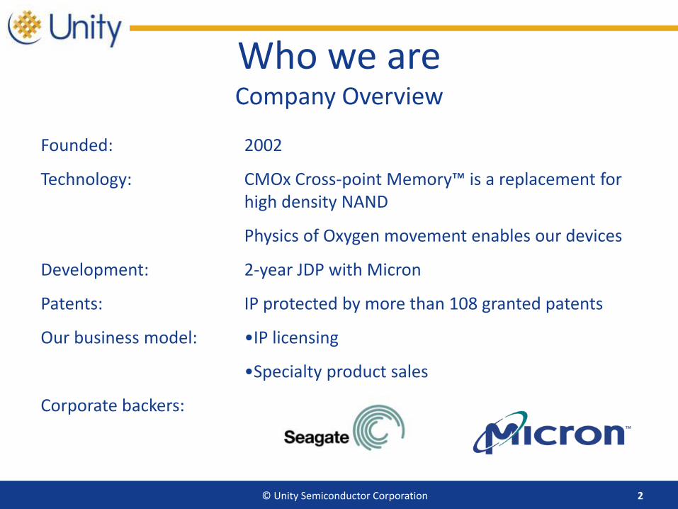
Who we areCompany Overview
© Unity Semiconductor Corporation 2
Founded: 2002
Technology: CMOx Cross-point Memory™ is a replacement for high density NAND
Physics of Oxygen movement enables our devices
Development: 2-year JDP with Micron
Patents: IP protected by more than 108 granted patents
Our business model: •IP licensing
•Specialty product sales
Corporate backers:
3
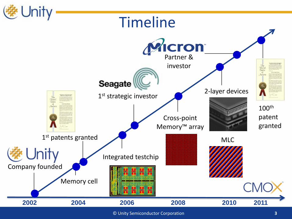
2002 2004 2008 20102006•Company founded •
Memory cell
1st patents granted
1st strategic investor •Cross-point
Memory™ array
•Partner & investor •
MLC
2-layer devices
•Integrated testchip
2011
••
© Unity Semiconductor Corporation
Timeline•
100th
patent granted
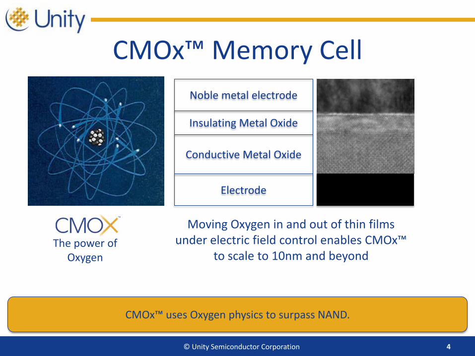
CMOx™ Memory Cell
© Unity Semiconductor Corporation 4
CMOx™ uses Oxygen physics to surpass NAND.
The power of Oxygen
Noble metal electrode
Insulating Metal Oxide
Conductive Metal Oxide
Electrode
Moving Oxygen in and out of thin films under electric field control enables CMOx™
to scale to 10nm and beyond
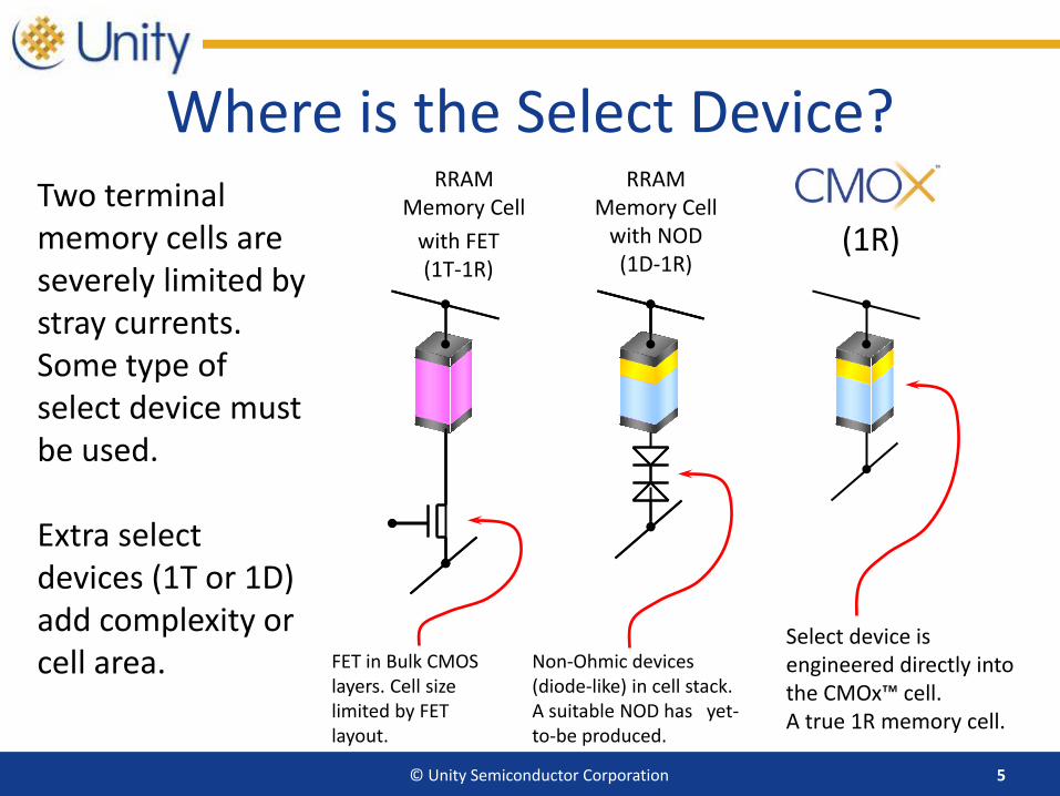
Where is the Select Device?
(1R)
RRAMMemory Cell
with NOD(1D-1R)
RRAMMemory Cell
FET in Bulk CMOS layers. Cell size limited by FET layout.
Two terminal memory cells are severely limited by stray currents. Some type of select device must be used.
Extra select devices (1T or 1D) add complexity or cell area. Non-Ohmic devices
(diode-like) in cell stack.A suitable NOD has yet-to-be produced.
Select device is engineered directly into the CMOx™ cell.A true 1R memory cell.
with FET(1T-1R)
© Unity Semiconductor Corporation 5
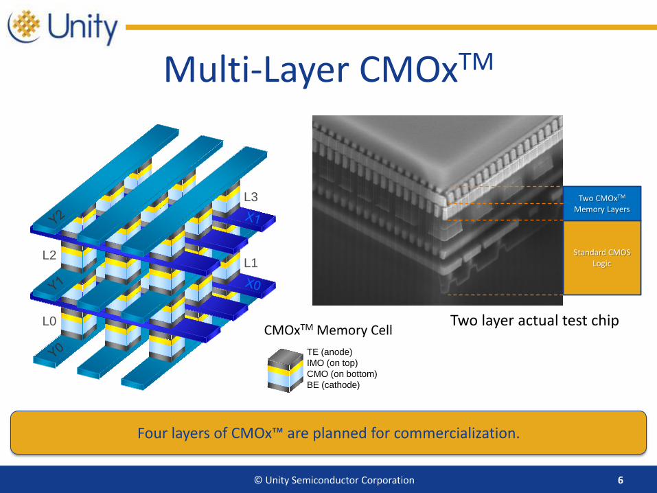
Two CMOxTM
Memory Layers
Standard CMOS Logic
Multi-Layer CMOxTM
L0
L1L2
L3
TE (anode)IMO (on top)CMO (on bottom)BE (cathode)
CMOxTM Memory Cell
© Unity Semiconductor Corporation 6
Four layers of CMOx™ are planned for commercialization.
Two layer actual test chip
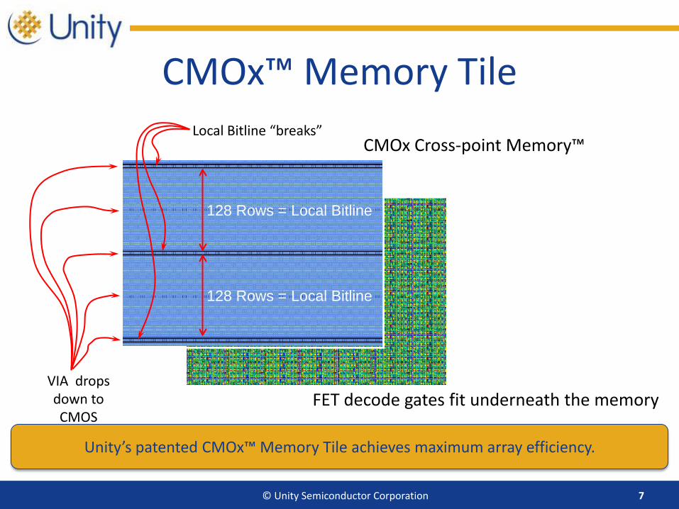
CMOx™ Memory Tile
FET decode gates fit underneath the memory
CMOx Cross-point Memory™
128 Rows = Local Bitline
VIA drops down to CMOS
128 Rows = Local Bitline
Local Bitline “breaks”
© Unity Semiconductor Corporation 7
Unity’s patented CMOx™ Memory Tile achieves maximum array efficiency.
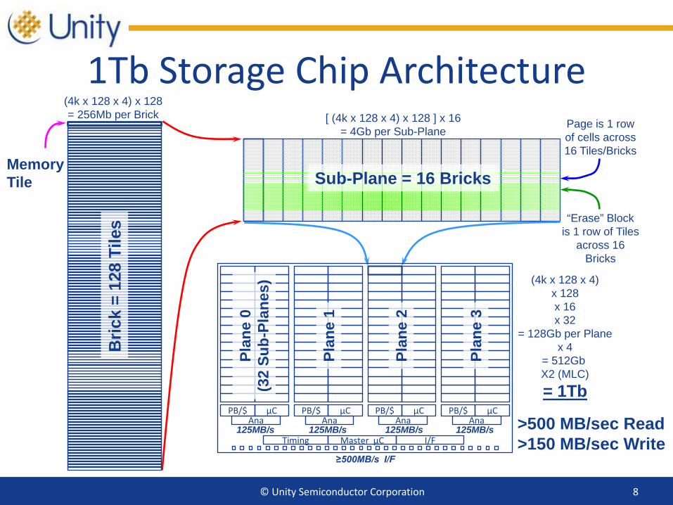
1Tb Storage Chip Architecture
Sub-Plane = 16 Bricks
Bric
k =
128
Tile
s(4k x 128 x 4) x 128= 256Mb per Brick
Memory Tile
[ (4k x 128 x 4) x 128 ] x 16= 4Gb per Sub-Plane
(4k x 128 x 4)x 128x 16x 32
= 128Gb per Planex 4
= 512Gb X2 (MLC)
= 1TbPB/$ µC
AnaPB/$ µC
AnaPB/$ µC
AnaPB/$ µC
Ana
Plan
e 0
(32
Sub-
Plan
es)
Plan
e 1
Plan
e 2
Plan
e 3
Timing Master µC I/F
Page is 1 row of cells across 16 Tiles/Bricks
“Erase” Blockis 1 row of Tiles
across 16 Bricks
125MB/s 125MB/s 125MB/s 125MB/s
≥500MB/s I/F
>500 MB/sec Read>150 MB/sec Write
8© Unity Semiconductor Corporation
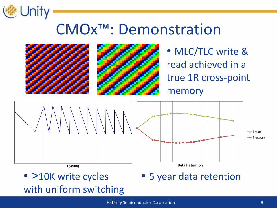
CMOx™: Demonstration
© Unity Semiconductor Corporation 9
• MLC/TLC write & read achieved in a true 1R cross-point memory
• 5 year data retentionData Retention
Erase
Program
• >10K write cycles with uniform switching
Cycling
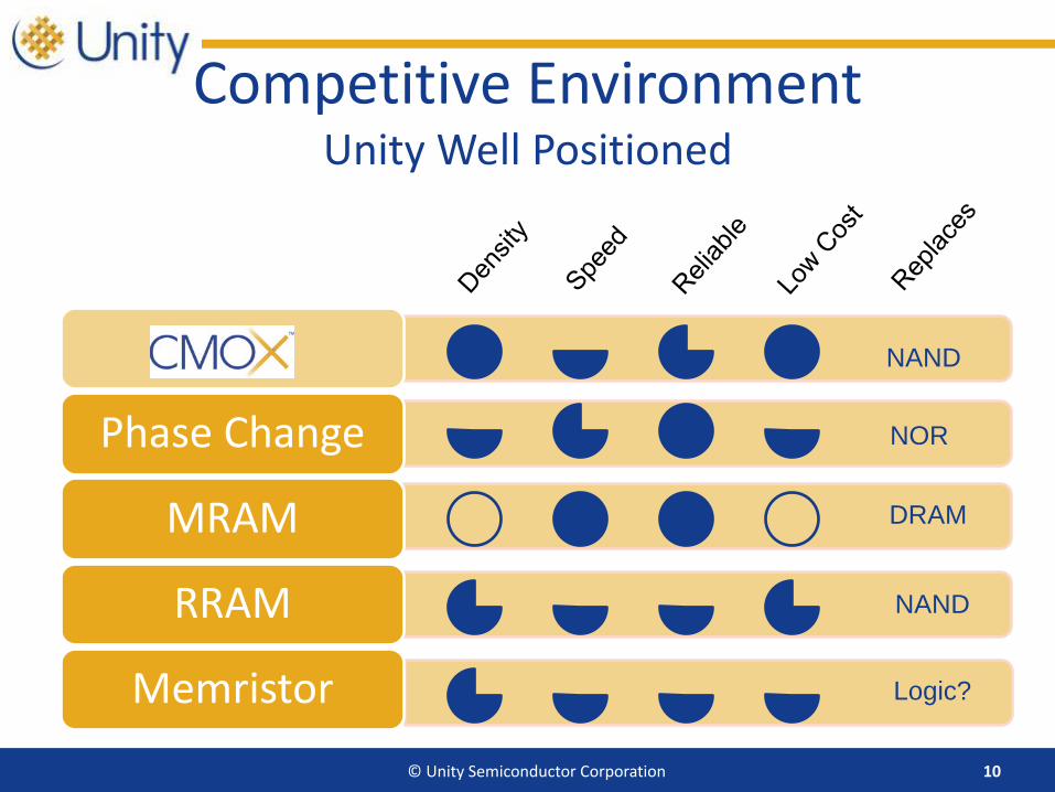
Competitive EnvironmentUnity Well Positioned
© Unity Semiconductor Corporation 10
Phase Change
MRAM
RRAM
Memristor
NAND
NOR
DRAM
NAND
Logic?

What We Offer Licensees
11
Process technology transferReference design
Patent license
Device scaling
expertise
Unity offers a comprehensive bundle of IP and engineering know-how to licensees.
© Unity Semiconductor Corporation
Access to Unity Engineers
Summary• We designed, architected and patented a transistorless
memory cell that we fabricate into ultra dense cross-point arrays.
• CMOx Cross-point Memory™ is engineered to replace NAND.
• Our Micron joint development program is scaling CMOx™ in a state-of-the-art 300mm fab using industry standard tools.
• CMOx Cross-point Memory™ will come to market through our licensing and technology transfer to memory semiconductor companies and through specialty chips we sell directly.
12© Unity Semiconductor Corporation
Technology for Terabits