Embed Size (px)
Citation preview

www.phi.com
Auger Electron Spectroscopy� Auger Electron Spectroscopy is an analytical technique that provides compositional
information on the top few monolayers of material.
� Detect all elements above He
� Detection limits:~1 - 0.1 atomic %
� Surface sensitive: top 4-50 Å
� Spatial resolution: < 80 Å Auger spatial resolution with Field Emission electron gun

www.phi.com
Common Auger Applications� Problem solving & failure analysis of nanostructures
� Advanced metallurgy impurity segregation and facture analysis
� Corrosion
� Thin film analysis
� Semiconductor and electrical components defect analysis

www.phi.com
What Information does Auger provide ?� Surface composition at high spatial resolution
» SEM imaging
• Provides high magnification visualization of the sample
» Elemental analysis
• Determines what elements are present & how much
» Elemental imaging
• Illustrates two-dimensional elemental distribution
� Sputter depth profiling
» Reveals thin film and interfacial composition
www.phi.com
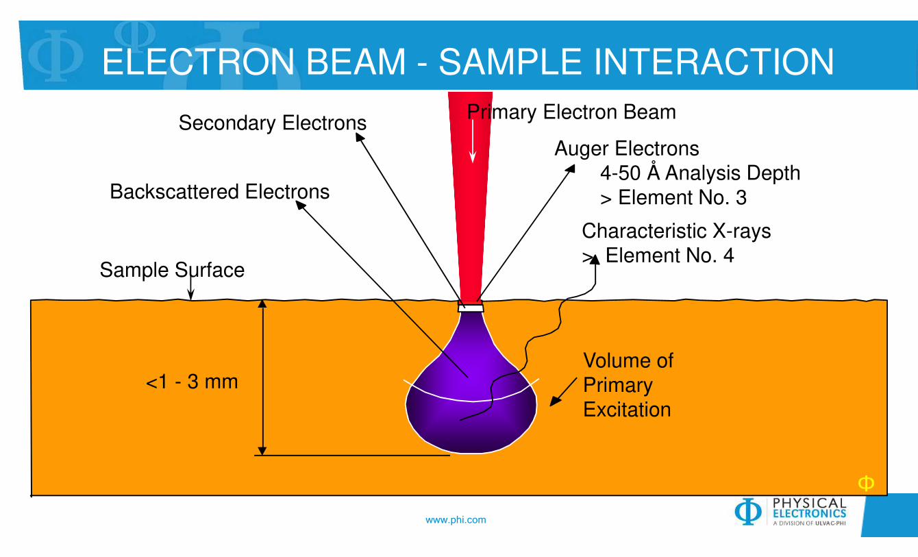
ELECTRON BEAM - SAMPLE INTERACTIONPrimary Electron Beam
Auger Electrons4-50 Å Analysis Depth> Element No. 3
Characteristic X-rays> Element No. 4
Volume of Primary Excitation
<1 - 3 mm
Sample Surface
Backscattered Electrons
Secondary Electrons
Φ

www.phi.com
IncidentBeam
Auger Electron
X-rayPhoton
X-ray Fluorescence Auger Electron Emission
Auger & X-ray Emission
IncidentBeam

www.phi.com
Auger and Fluorescence Yields
ρA + ρX = 1
www.phi.com
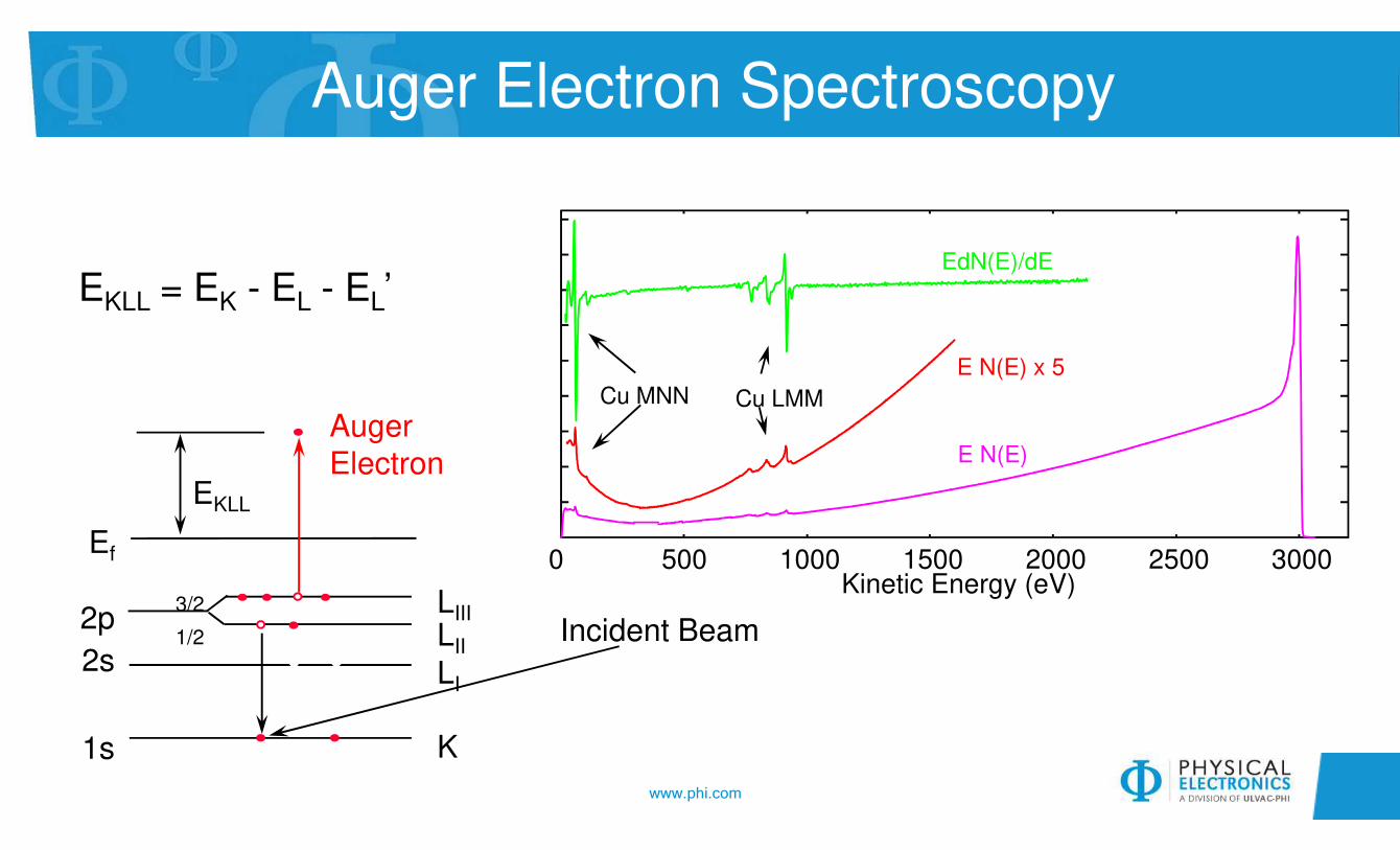
Auger Electron Spectroscopy
2p
1s
2s1/2
3/2
Ef
K
LI
LII
LIIIIncident Beam
EKLL = EK - EL - EL’
AugerElectron
EKLL
0 500 1000 1500 2000 2500 3000Kinetic Energy (eV)
E N(E)
E N(E) x 5
EdN(E)/dE
Cu LMMCu MNN
www.phi.com
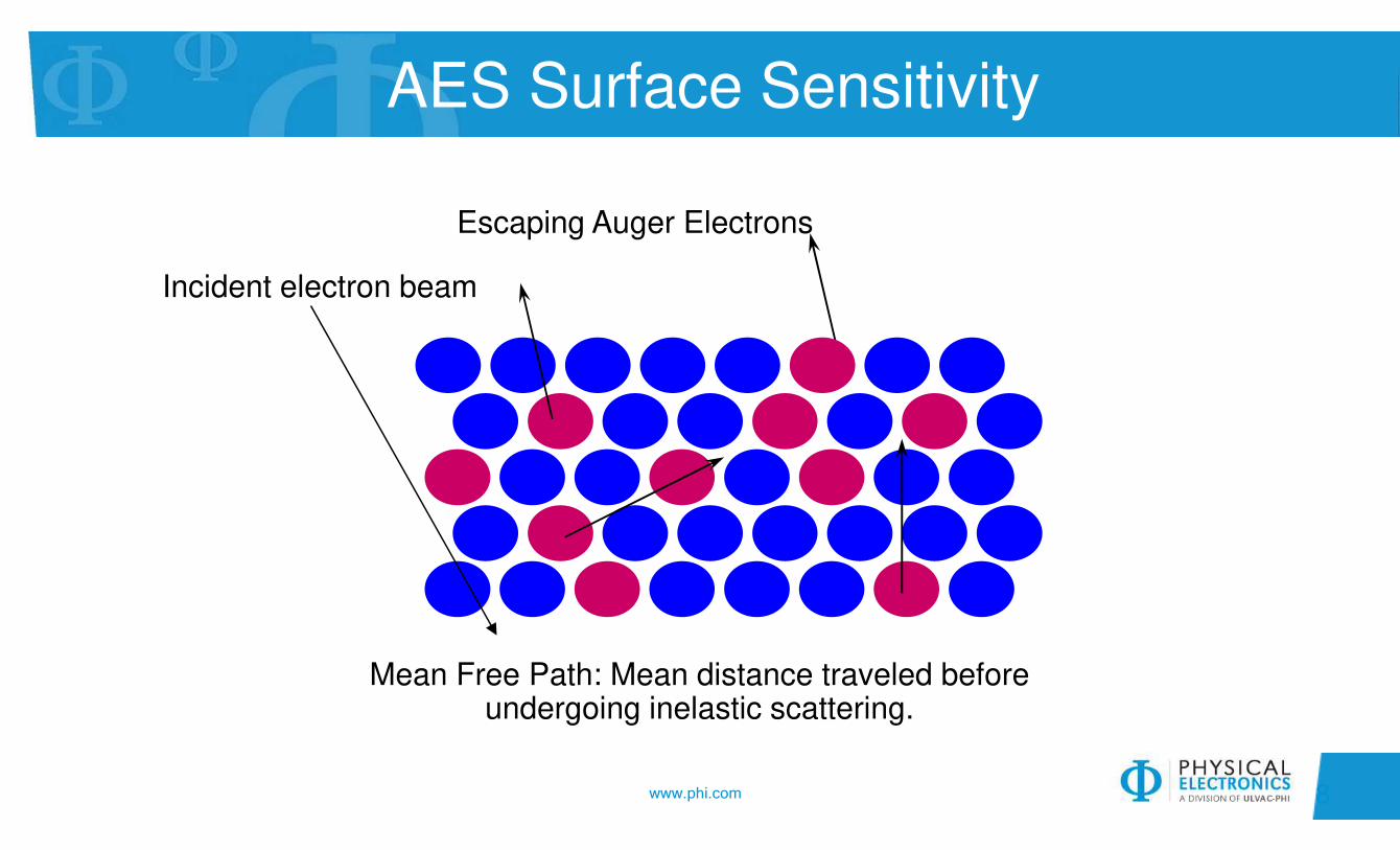
AES Surface Sensitivity
8
Incident electron beam
Escaping Auger Electrons
Mean Free Path: Mean distance traveled before undergoing inelastic scattering.

www.phi.com
Auger Electron Analysis Depth
Various thicknesses of Au on Si. The high energy Si KLL peak has a greater analysis depth than the low energy Si LMM peak.
Thickest Au
Thinner Au
Clean Si
Si KLLSi LMM
Si LMM
Au AuAu
Si KLL
Au
AuAu
Au
Si KLLAu
O
O

www.phi.com
Schottky Field Emission Optics
Beam Current (nA)
100
1000
10000
1 10 50
20 kV
10 kV
5 kV
3 kV
Bea
m D
iam
eter
(Å
)Typical Beam Size - PHI 680
(20% - 80%)

www.phi.com
Auger Line Scan across Abrupt Interface
Primary beam20 keV
Ag MVV@ 355 eV

www.phi.com
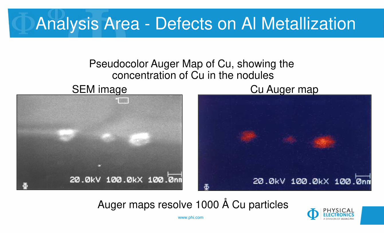
Analysis Area - Defects on Al MetallizationSample Description
� Metallization in semiconductor device manufacturing
» TiN / Al(Cu) on SiO2
� Defects are found along edge of metal lines after a plasma etch processing step
� Auger analysis is required to determine the defect composition

www.phi.com
Aluminum lines at 20,000X, showing nodules
Analysis Area - Defects on Al Metallization
www.phi.com
SEM image Cu Auger map
Auger maps resolve 1000 Å Cu particles
Pseudocolor Auger Map of Cu, showing the concentration of Cu in the nodules
Analysis Area - Defects on Al Metallization

www.phi.com
Analysis Area - Defects on Al Metallization
Spectra on the particle includes Auger signal from the surrounding material due to backscatter electrons.
500 1000 1500 2000Kinetic Energy (eV)
Peak to Peak Height
Point 1 - On the Particle
Point 2 - Line Top Surface
Point 3 - Line Sidewall
Ti(N)Ti O Cu Al Si
Ti(N)Ti
O Al Si
Ti O Al Si
dEN
(E)/
dE

www.phi.com
Backscatter Effects~1.3µm Si Particle on SiO2
SEM of ~1.3µm Particle on SiO2 SEM of Particle in f.e. AES
Primary electron scattering results in a minimum feature size from which all of the Auger signal originates
This minimum feature size depends on sample geometry, feature composition, and primary beam energy

www.phi.com
Backscatter Effects vs. Beam Voltage ~1.3µm Si Particle on SiO2
O, C and Ti are from the substrateLow voltage minimizes backscatter signal
SiSi
O
5 kV Si
Si
SiSi
O
7 kV
Si
Si
OC
10 kV SiSi O
C Ti
20 kV

www.phi.com
QuantificationSensitivity Factors
� Assuming Auger yield varies linearly with concentration
� Assuming homogeneous distribution
� CX = (IX / SX) / (Σi (Ii / Si)
� SX may depend on sample matrix & chemistry, as well as specific analytical instrument

www.phi.com
Sensitivity Factors: Si and SiO2
Si
O
Si
Using sensitivity factors for elemental SiSi:O => 74:26Using sensitivity factors for Si OxideSi:O => 33:67
-30
-20
-10
0
10
20
500 1000 1500 2000Kinetic Energy (eV)

www.phi.com
Compucentric Zalar Rotation Depth Profiling
20
0 50 100 150 200 250 3000
20
40
60
80
100
Sputter Time (min)
Ato
mic
Conce
ntr
atio
n (
%)
O
Al (oxide)
Al (metal) Si
Compucentric Zalar Depth Profile of 10 µm Via Contact
Secondary Electron Image
(Before Sputtering)
www.phi.com
Compucentric Zalar Rotation Depth Profiling
21
0 50 100 150 200 250 3000
20
40
60
80
100
Sputter Time (min)
Ato
mic
Conce
ntr
atio
n (
%)
O
Al (oxide)
Al (metal) Si
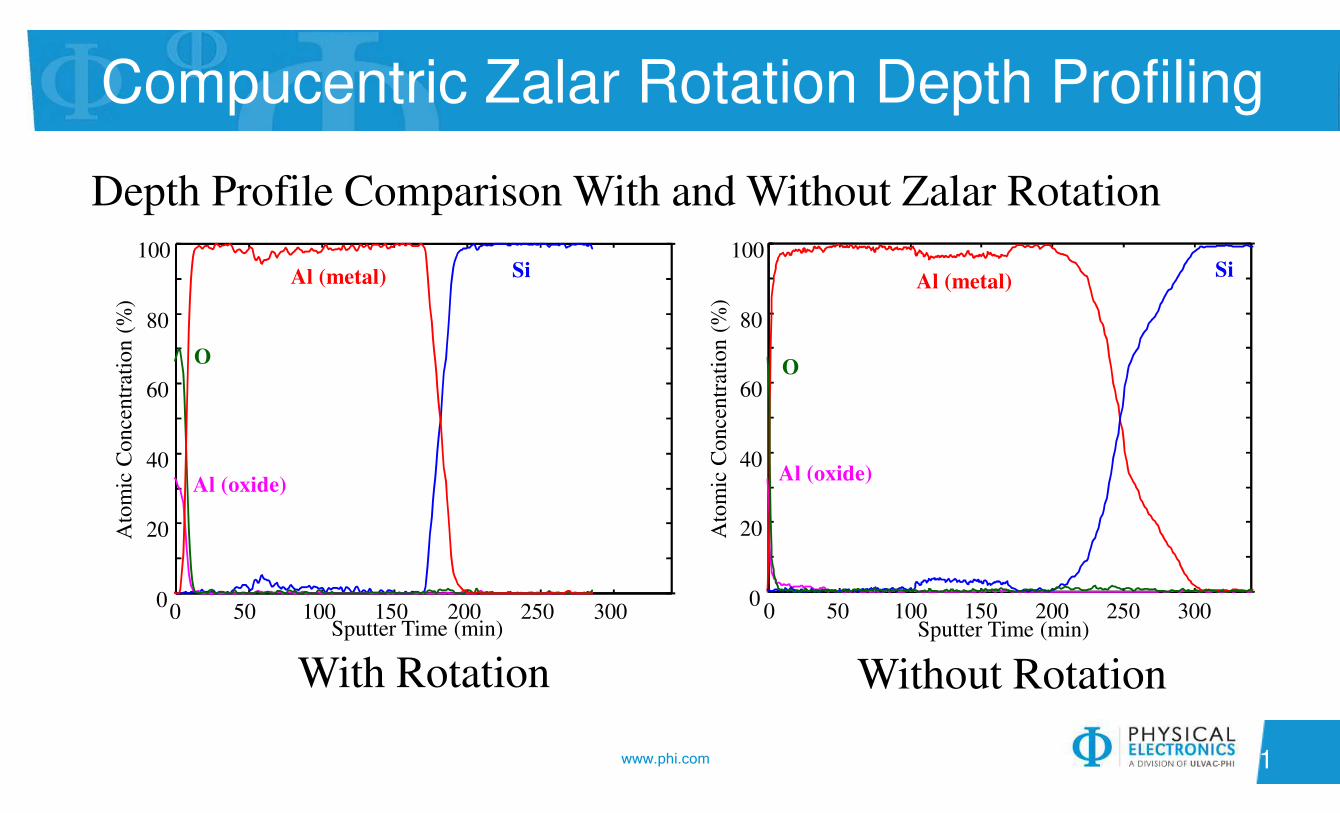
Depth Profile Comparison With and Without Zalar Rotation
0 50 100 150 200 250 3000
20
40
60
80
100
Sputter Time (min)
Ato
mic
Conce
ntr
atio
n (
%)
Al (metal)
O
Al (oxide)
Si
Without RotationWith Rotation

www.phi.com
Compucentric Zalar Rotation Depth Profiling
22
Without RotationWith Rotation
2500X2500X
SE Images of 10 µm Via Contactsafter Depth Profiling