Embed Size (px)
Citation preview

1114/TY/Pre_Pap/Elec/2014/CP/Class/AVE_Soln 1
500 Hz 2500 Hz 12.5 Hz Frequency
Inte
nsit
y in
dB
40 dB
30 dB
Audio level without preemphasis
Tape noise level which is comparable with signal at high frequencies and may even exceed it
(a)
T.Y. Diploma : Sem. V [EN/EX/EJ/DE/ED/EI]
Audio Video Engineering Time: 3 Hrs.] Prelim Question Paper Solution [Marks : 100
Q.1(a) Attempt any THREE of the following : [12]Q.1(a) (i) Draw and explain Dolby-NR System. [4](A) Dr. Ray Dolby introduced a novel system for providing 10 15 dB
improvement in recording and playback tapes. In normal pre-emphasis, it is presumed that weak intensity is present only in high frequencies. This is not always the case. All weal signals, irrespective of frequencies need to be emphasized. This difficulty is solved by Dolby as explained below :
When the strength of signals falls below a pre-determined level (say, 40 dB over the noise level), the circuits boost the strength before recording. All signals which are 40 dB or higher, pass through the Dolby system direct without any change. The lower level signals pass through the boosting stages which boost these signals by 10 15 db. Boosting is done before recording. Signal in the absence of boosting is shown in Figure 1.
(a) After boosting, recording noise remains unchanged but signal is boosted
as shown in Figure 1(a). (b) During playback, signal and noise both are both are reduced as shown in
Figure 1(b). (c) Thus, Figure 1(c) indicates that signal to noise ratio is finally improved.
Vidyidididy
Inte
nsit
y in
dB
n d
B
40 dB40 d
30 dB
dyAudio ledio le(a) a) dy
alank
ar
[12][1[4][4]
viding 10 10 15 dB 15 dB rmal pre-emphasis, it is -emphasis, it is
gh frequencies. This is not quencies. This is note of frequencies need to be of frequencies need to
y as explained below : xplained below :
ow a pre-determined level (say, 4re-determined lev oost the strength before recorhe strength before
pass through the Dolby system dirh the Dolby systgnals pass through the boosting pass through the
15 db. Boosting is done before re 15 db. Boosting is done bef shown in Figure 1. hown in Figure 1.
recording noise remains unchangding noise remains u igure 1(a). (a).
playback, signal and noise both ak, signal and noise e 1(b).
Thus, Figure 1(c) indicates that , Figure 1(c) indica
arks
r

Vidyalankar : T.Y. Diploma AVE
2
Q.1(a) (ii) Explain the different types of lenses used in CD player. [4](A) CD Lens
Collimation Lens The collimator lens is used to produces completely parallel beams of laser. This lens together with the objective lens is used to focus the laser beam to the disc surface.
Concave Lens (In Single-Beam Linear Optical Block) In single-beam linear optical block assembly this concave lens is used to concentrate the laser beam, reflected from the disc surface, onto the photo diode array. This lens is mainly used to improve the sensitivity of the photo diode array.
Quarter Wave Plate (In Three-Beam Linear Optical Block) The direct laser beam going towards the disc surface, when passed through this plate gets optically rotated by 45 degree. The reflected laser beam is
500 Hz
12.5 Hz
40 dB
30 dB
10 dB separation
Tape noise level (it gets reduced due to deemphasis circuit)
Frequency (c)
Audio level after deemphasis
(c)
Fig.1 (Countd.) : (c) Position after de-emphasis
500 Hz 2500 Hz 12.5 Hz
40 dB
30 dB
Audio level after preemphasis before recording
10 dB separation
Tape noise level (no change)
Frequency
(b)
Fig.1 (Count.): Reduction of noise by 10 dB in Dolby system (a) Position without pre-emphasis (b) Position after pre-emphasis
Vidy
alank
arplain the different types of lenplain the different types
ens ns limation Lens on Len
The collimator lens is used to ollimator lens is used This lens together with the oThis lens together with the the disc surface. he disc surface.
Concave Lens (In SiConcave LenIn single-beam linIn single-bconcentrate theconcdiode array. diodediode arra
Qua
ananlalalalalalalalalalaalaaalalaaaaaaaaaalaalalaalalaaaanlaan Hz
12.5 Hz 12.5 Hz
lalan10 dB sea Taprl(c)(c)
dio level after deemphasis after deemphasis
Fig.1 (Countd.) :untd (c) Position after de (c) Position
ka
n Dolby system ystem n after pre-emphasis n after pre-emphasis

Prelim Question Paper Solution
3
Fig.: Cylindrical Lens to get Focus Error
further rotated by 45 degree, when the beam pass through this for the second time. This cause the optical polarization between the direct laser beam, going towards the disc, and the reflected laser beams to differ by 90 degree. The reflected beam is now of the correct polarization to enable efficient deflection of it within the prism, towards the photo-diode array.
Objective Lens Before hitting the disc surface, the laser beam comes out of the pick-up assembly through an objective lens. The objective lens is used to focus the laser beam onto the CD surface and to receive the reflected laser beam. This lens is moved up/down to achieve the focus of the laser beam on the disc surface. The objective lens is always kept in focus using a system similar to the voice coils system used in the audio speakers. It is also moved horizontally in the linear pick-up assembly to keep the laser beam in proper track. In players that use the radial tracking method the objective lens unit does not move horizontally (laterally).
Cylindrical Lens (In Three-Beam Linear Optical Block) The main function of this lens is to enable the reflected beam from the CD to assist in creating the necessary signal to make sure that focus of the laser beam on the playing surface of the disc is maintained.
Vidy
alank
arFig
o ee array. ay.
out of the pick-up f the pick-up s is used to focus the ed to focus the
e reflected laser beam. ted laser beam.s of the laser beam on the s of the laser beam on th
kept in focus using a system pt in focus using a sys audio speakers. It is also moved peakers. It is als
ly to keep the laser beam in pro keep the laser beam racking method the objective len method the obje
y).
Cylindrical Lens (In indrical Lhe main function
eating the urfa
Vidyalankar : T.Y. Diploma AVE
4
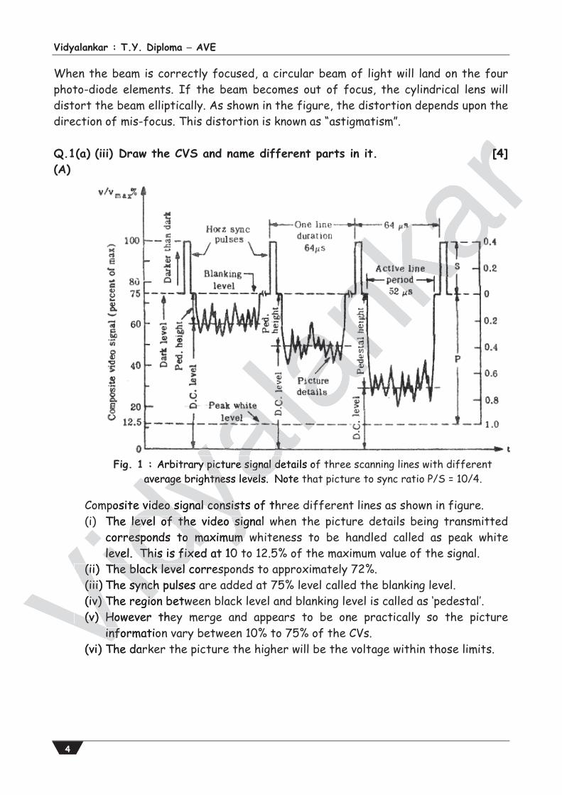
Fig. 1 : Arbitrary picture signal details of three scanning lines with different average brightness levels. Note that picture to sync ratio P/S = 10/4.
When the beam is correctly focused, a circular beam of light will land on the four photo-diode elements. If the beam becomes out of focus, the cylindrical lens will distort the beam elliptically. As shown in the figure, the distortion depends upon the direction of mis-focus. This distortion is known as “astigmatism”. Q.1(a) (iii) Draw the CVS and name different parts in it. [4](A)
Composite video signal consists of three different lines as shown in figure.
(i) The level of the video signal when the picture details being transmitted corresponds to maximum whiteness to be handled called as peak white level. This is fixed at 10 to 12.5% of the maximum value of the signal.
(ii) The black level corresponds to approximately 72%. (iii) The synch pulses are added at 75% level called the blanking level. (iv) The region between black level and blanking level is called as ‘pedestal’. (v) However they merge and appears to be one practically so the picture
information vary between 10% to 75% of the CVs. (vi) The darker the picture the higher will be the voltage within those limits.
Vidy
alank
ar : Arbitrary picture signal details ofy picture signal daverage brightness levels. Note taverage brightness levels.
[4][
posite video signal consists of th video signal consist) The level of the video signal level of the video sig
corresponds to maximum wesponds to maximum level. This is fixed at 10level. This is fix
(ii) The black level corres (ii) The black level (iii) The synch pulses ar (iii) The synch (iv) The region betwiv) The regio (v) However the (v) Ho
informatioinfo (vi) The dar

Prelim Question Paper Solution
5
Q.1(a) (iv) Explain separation of u and v signal with the help of block diagram.
[4]
(A) Separation of U A V signal As we known that in the transmitter both U A V are combined with each other. Hence we have to separate them in the receiver. For V signal, For line N the phase shift is +90°, therefore the equation for combine signal can be written as u+jv. For the next line [+1] the V signals have a phase shift of -90°. Hence the equation of combined signal is u-jv. For separation purpose we sub & add the signal u+jv & u-jv as shown in figure.
Actually, the operation of u & v signal is done with the help of transformer action. As known in figure it consists of transistor Qi, transformer Tl, centre tapped transformer T2 and PAL Delay iine. The signal after passing through PAL Delay line appears across winding A of centre tapped transformer. The colour signal is also directly fed to the centre point of transformer via potentiometer R2- Thus, delay line provides the signal to the centre tapped transformer having equal magnitude and opposite phase in winding A <& B. On the other hand the direct signal induces in winding A & B. Thus, addition takes place in winding B hence we get U signal at winding B since subtraction takes place in winding A hence we get V signal across winding A.
Vidy
alank
ar
thal, For lr l
signal can be can phase shift of -ift of
separation purpose ation purpose
f u & v signal is done with the h u & v signal is done with figure it consists of transistort consists of tra
sformer er TT22 and PAL Delay iine. and PAL Delaelay line appears across windine appears acro
The colour signal is also directolour signal is alsoer via potentiometer R2- Thus, otentiometer R2
re tapped transformer ransformer having eqhang A <& B. On the other hand theg A <& B. On the ot
us, addition takes place in winddition takes place since subtraction takes place i subtraction takes plawinding A. winding A

Vidyalankar : T.Y. Diploma AVE
6
The detail circuit of operation of U & V signals is as shown below :
Q.1(b) Attempt any ONE of the following : [6]Q.1(b) (i) Write a short note on Vidicon Camera tube. [6](A)
The Vidicon came into general use in the early 50’s and gained immediate popularity because of small size and ease of operation.
It functions on the principle of photoconductivity, where the resistance of the target material shows a marked decrease when exposed to light. Figure 2, illustrate the structural configuration of a typical Vidicon, and Figure 2 shows the circuit arrangement for developing camera signal output.
Fig. 1 : Vidicon camera tube cross-section
Vidy
alank
aring :
Vidicon Camera tube. Vidicon Camera tube.
The Vidicon came inThe Vidicon cpopularity becauseopula
It functions funtarget ma
FiF g. 1 :
Vid

Prelim Question Paper Solution
7
As shown there, the target consist of a thin photo conductive layers of either selenium or antimony compounds.
This is deposited on a transparent conducting film, coated on the inner surface of the face plate. This conductive coating is known as signal electrode or plate.
Image side of the photo layer, which is in contact, with the signal electrode is connected to DC supply through the load resistance RL.
The beam that emerges from the electron gun is focussed on surface of the photo conductive layer by combined action of uniform magnetic fields of an external coil and electrostatic field of grid No. 3.
Grid No. 4 provides a uniform decelerating field between itself, and the photo conductive layer, so that the electron beam approaches the layer, with a low velocity to prevent any secondary emission.
Deflection of the beam for scanning the target, is obtained by vertical and horizontal deflecting coils, placed around the tube.
Q.1(b) (ii) Explain the working of Dish Antenna used in cable TV and give
it’s specification. [6]
(A) Dish Antenna Why dish antenna having meshy structure : While installing the dish antenna look angles are taken into consideration. Once look angle adjusted installation should not be disturbed.
Fig. 2 : Circuit for output signal from a Vidicon camera tube
+40V
R = 2M R = 20M
Vidy
alank
art of a thin photo conductive laye thin photo conductiv
.
parent conducting film, coated onarent conducting film, coonductive coating is known as signve coating is know
oto layer, which is in contact, w yer, which is in cont upply through the load resistanc hrough the load re
t emerges from the electron guges from the electuctive layer by combined actioner by combined
coil and electrostatic field of gr coil and electrostatic fiel
d No. 4 provides a uniform dece 4 provides a uniformconductive layer, so that the elconductive layer, so that the velocity to prevent any secondvelocity to prevent any second
Deflection of the beam Deflection of the horizontal deflecting chorizontal def
Q.1(b) (ii) Explain thQ.1(b) (ii) it’s spei
) Dish AntV
or output signal ut signal on camera tube era tu

Vidyalankar : T.Y. Diploma AVE
8
Due to atmospheric changes like rain, winds there is a possibility of change in look angle of dish, due to meshy structure, rain and wind will go through holes by keeping fix position of dish antenna.
The parabola is a plane curve defined as the locus of a point which moves so that its distance from another point (called the focus) plus its distance from a straight line (directrix) is constant. These geometric properties yield an excellent microwave or light reflector.
Principle : The parabolic reflector collects all the electromagnetic waves from satellite due to parabolic shape reflected rays concentrate at focal point which gives the high gain signal.
Fig.: Geometry of parabola.
The ratio of the focal length to the mouth, diameter (AF/CD) is called aperture of the parabola just as in camera lenses. A practical reflector employing the properties of the parabola will be a
three dimensional bowl-shaped surface, obtained by revolving the parabola about the axis AB.
The resulting geometric surface is the paraboloid, often called a parabolic reflector or microwave dish.
When it is used for reception exactly the same behaviour is manifested, so that this is also a high gain receiving directional antenna reflector.
The principle of reciprocity which states that the properties of an antenna are independent of whether it is used for transmission or reception.
The reflector is directional for reception because only the rays arriving from BA direction i.e. normal to the directrix are brought together at the focus.
On the other hand, rays from any other direction are canceled at that point, again owing to path length differences.
Vidy
alank
arr
es
rce fro
ar
yield a
arkar
kartromagnetic waves
ka
rays concentrate at foc
kakaan
ka
alFig.: Geometry
yao of the focal length to the m focal length tore of the parabola just as in camre of the parabola just as
A practical reflector employing actical reflector ethree dimensional bowl-sharee dimensional bowparabola about the axis ABrabola about the axis A
The resulting geometric The resulting geometric reflector or microwavreflector or mi
When it is used foWhen so that this is a hat t
The principl antenna aarecepti
The fr
Prelim Question Paper Solution
9
The reflector provides a high gain because like the mirror of a reflecting telescope, it collects radiation from a large area and concentrates it all at the focal point.
Specifications of Dish Antenna : (i) Size 8 feet (ii) Gain 36 dB (iii) Band C (3.7 to 4.2 GHz downlink frequency) (iv) Look angle 360° rotation in azimuth, 18 to 90° rotation in elevation
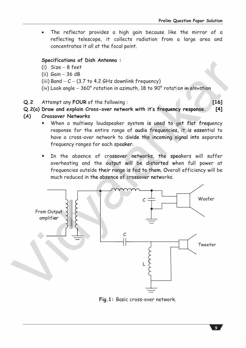
Q.2 Attempt any FOUR of the following : [16]Q.2(a) Draw and explain Cross-over network with it’s frequency response. [4](A) Crossover Networks
When a multiway loudspeaker system is used to get flat frequency response for the entire range of audio frequencies, it is essential to have a cross-over network to divide the incoming signal into separate frequency ranges for each speaker.
In the absence of crossover networks, the speakers will suffer overheating and the output will be distorted when full power at frequencies outside their range is fed to them. Overall efficiency will be much reduced in the absence of crossover networks.
C
L
C
From Outputamplifier
Woofer
Tweeter
Fig.1: Basic cross-over network.
Vidy
adydydydyyydydy
alank
arrrararkar n elevation
[16][’s frequency response. [4] frequency response.
em is used to get flat freque used to get flat audio frequencies, it is essent frequencies, it i
divide the incoming signal into the incoming sigeaker.
rossover networks, the speakrossover networks, the e output will be distorted wh output will be distort
e their range is fed to them. Ove range is fed to th the absence of crossover netwo bsence of crossover
alalalalald
alyaidya
dddydddddaa
dydydydy
pututfier

Vidyalankar : T.Y. Diploma AVE
10
Crossover network make use of the fact that the capacitive reactance decreases with increase in frequency [Xc = 1/(2 fC)], and the inductive reactance increases with increase in frequency (X1 = 2 fL). A basic crossover network is illustrated in Figure 1.
The circuit consists of a low pass L C filter across the woofer and a high pass L C filter across the tweeter. The low pass filter permits only low audio frequencies (16 Hz to 1000 Hz) to go to the woofer. The series reactance of L and shunt reactance of C for high audio frequencies prevents these frequencies from going to the woofer.
The high pass filter consisting of C in series and L in shunt allows the high audio frequencies to pass to the tweeter and blocks the low frequencies.
The response curve of a typical crossover network (Figure 1) is shown in Figure 2. It gives attenuation of 12 dB per octave.
Equations (1) and (2) give the values of L and C
L
c
R 2L
2 f ... (1)
c L
1C
2 f R 2 ... (2)
where, RL is the impedance of loudspeaker in ohms and fc is the crossover frequency in Hz, L is the inductance and C, the capacitance of LC circuits.
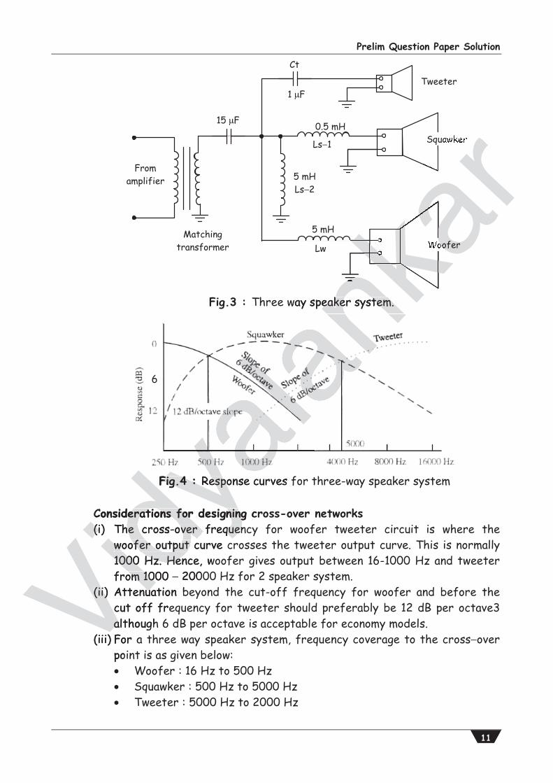
A commercial three way divider network is shown in figure 3. In this circuit, capacitor Ct of 1 F in series with tweeter prevents low and mid frequencies from reaching the tweeter. Similarly, inductance Lw of 5 mH in series with woofer prevents high frequencies from reaching the woofer.
Inductances Ls 1 and Ls 2 of 0.5 mH and 5 mH, respectively in squawker
circuit allow only mid frequencies and prevent too low and too high frequencies from reaching the squawker.
Typical divider curve for three way network of Figure 3 is shown in figure 4 single element in filtering gives attenuation of 6 dB per octave and double elements give 12 dB per octave.
0 dB
3 dB
1000Hz 2000 4000 8000 16000Hz
Fig. 17 : Response curve of basic cross-over network
Vidy
alans (1) and (2) give the values of Lnd (2) give the value
yyyL
cc
R 2LLL2 f2 fcc
dydydyc Lc L
1CC
2 f R 22 f Rc Lc L
where, Rhere L is the impedanc the impedanL
frequency in Hz, L is thefrequency in Hz A commercial three A commercial
capacitor Cpacitor t of 1t
from reaching woofer prevw
Inductan Icircuifre
alank
ar
and a hi hirmits only low only lo
ofer. The series e seri audio frequencies o frequencies
er. L in shunt allows the high hunt allows the high
ocks the low frequencies. ocks the low frequencies. network (Figure 1) is shown in etwork (Figure 1) is show
er octave. ve.
nkannk
alaaalaaala1000HzHz 2000 4000
g. 17 : Response curve of basic cResponse curve of
Prelim Question Paper Solution
11
Considerations for designing cross-over networks (i) The cross-over frequency for woofer tweeter circuit is where the
woofer output curve crosses the tweeter output curve. This is normally 1000 Hz. Hence, woofer gives output between 16-1000 Hz and tweeter from 1000 20000 Hz for 2 speaker system.
(ii) Attenuation beyond the cut-off frequency for woofer and before the cut off frequency for tweeter should preferably be 12 dB per octave3 although 6 dB per octave is acceptable for economy models.
(iii) For a three way speaker system, frequency coverage to the cross over point is as given below:
Woofer : 16 Hz to 500 Hz Squawker : 500 Hz to 5000 Hz Tweeter : 5000 Hz to 2000 Hz
Lw
5 mH
5 mHLs 2
0.5 mH
Ls 1
Fromamplifier
Matchingtransformer
15 F
Ct
1 FTweeter
Squawker
Woofer
Fig.3 : Three way speaker system.
Fig.4 : Response curves for three-way speaker system
6
Vidy
a
Considerations for designing crerations for designing(i) The cross-over frequen(i) The cross-over frequen
woofer output curve cwoofer output 1000 Hz. Hence, wo1000 Hz. Henfrom 1000 om 10 200
(ii) Attenuation b(ii) Attenuacut off frealthough a
(iii) For a poi
nkaraakknka
nknknknkkkkkkkkr
kaoofer
way speaker system.eaker system.
yayaaayaFig.4 : Fig.4 : Response curves Respo

Vidyalankar : T.Y. Diploma AVE
12
Fig.1 : A three phase n-channel MOS charge coupled device (a) construction (b) transfer of electron between potential wells (c) different
phases of clocking voltage waveform.
While for two way speaker system, it is as follows : Woofer : 16 Hz to 1000 Hz Tweeter : 1000 Hz to 20000 Hz (iv) Inductors and capacitances should be calculated correctly. (v) Electrolytic capacitors cannot be used as there is no polarization D.C.
current. Q.2(b) What is CCD? Give it’s advantage and disadvantage over Camera tube. [4](A) CCD consists of MOS capacitors on a layer of SiO2 and n or P type substrate
as shown it consists of very closely spaced MOS capacitor.
The capacitor can store and transfer the charges generated in them due to light intensity. As shown the chip consists of P type substrate which is covered with an insulator SiO2.
Then the metallic gates are deposited on SiO2. Each gate creates one MOS capacitor thus a large number of MOS capacitor can be formed on entire surface of tube.
Now if the potential is applied to any of the gates, the holes in p type substrate under that gate will be repelled away and a depletion region will be formed, this depletion region is known as potential wells”.
When the light, from scene falls on the wells electrons are generated. Within it these electrons are attracts towards the gate and they are accumulated towards the surface.
The number of electrons generated depends upon the intensity of light. As a result, the charges at top of substrate represents the optical image.
Potential wells
MOS, Capacitor
Fig.1 : Fig.1 A threconstruction (b) tconstructi
When the WheWithin accum
lanka
r
zation D D
Camera tube. [4]a tube. [4] n or P type substrate type substrate
acitor.es generated in them due to es generated in them due
of P P type substrate which is type substrate whic
n SiO22. Each gate creates one M. Each gate creOS capacitor can be formed onpacitor can be for
d to any of the gates, the ho any of the gate ill be repelled away and a depleti ill be repelled away and a
gion is known as potential wells”. on is known as potential
Prelim Question Paper Solution
13
Charge Transfer The charge of one element is transferred along the surface of silicon chip by applying a more +ve voltage to the adjacent electrodes or gate while reducing the voltage on it. The minority carriers (electrons in this case) while accumulating in the wells reducing their depth and gets shifted to adjacent well. This docking sequence continues and charges finally reaches the end of the array, where the diode having capacitance from 1 to 2 pf collects them. Like this the information per line from every MOS capacitor gets converted into charge across the cap.
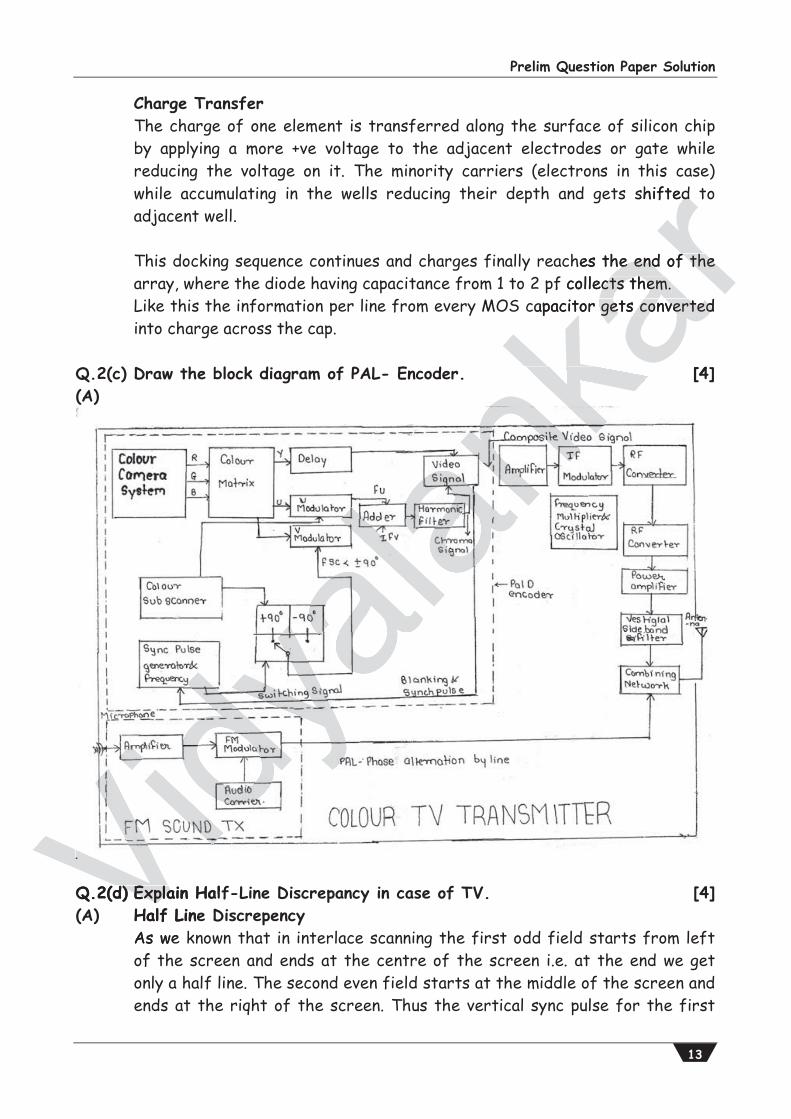
Q.2(c) Draw the block diagram of PAL- Encoder. [4](A)
Q.2(d) Explain Half-Line Discrepancy in case of TV. [4](A) Half Line Discrepency
As we known that in interlace scanning the first odd field starts from left of the screen and ends at the centre of the screen i.e. at the end we get only a half line. The second even field starts at the middle of the screen and ends at the riqht of the screen. Thus the vertical sync pulse for the first
Vidy
alank
ar
is shifted ed
hes the end of the he end of the pf collects them. ects them.
capacitor gets converted tor gets converted
[4
Q.2(d) Explain Halfd) Expla) Half Line
As we f t

Vidyalankar : T.Y. Diploma AVE
14
odd field will come at end of half line period end the second vertical sync pulse will arrive at the end of full line period. This results in misalignment of 1he horizontal pulse i.e. they do not appear one above the other but they appears at half line interval. In the TV we have circuit known as Sync separator, which is basically a clipper circuit. The input to the circuit is a composite video signal, this circuit clips the 0 to 75% waveform of CVS and thus produces only horizontal sync pulse and vertical sync pulse at the output. Now to separate H sync pulse and V sync pulse from each other we make use of High pass filter (differentiator) and Low pass filter (Integrator). The differentiator separates H sync pulse by converting them in to spike. The differentiator is form by using C1 and R1. The integrator separates V sync pulse by converting it into sawtooth waveform. The integrator is form using R2 and C2. The capacitor C2 charges during the vertical sync pulse time and produces sawtooth waveform. The same capacitor C2 also charges during horizontal sync pulse time to a small amplitude and also discharges fully because duty cycle of horizontal sync pulse is less.
Now let us see what happens at the end of even fields. In case of even fields capacitor C2 charges for horizontal sync pulse and also discharges. For even field the gap between the last horizontal sync pulse and vertical pulse is full line, therefore C2 charges and discharges to zero and then we get vertical sync pulse. Thus at the end of even field for the vertical sync pulse, capacitor C2 charges from zero.
Now let us see what happens at the end of odd fields.
The gap between the last horizontal sync pulse is half line because of which capacitor CZ charges but do not discharges to zero, when the sync, pulse appear. It means that at the end of odd field when capacitor CZ smarts charging for vertical sync pulse then at the beginning of charging its voltage is not zero. Thus at the end of odd field the capacitor CZ will charge to more voltage and it will charge early compare to the end of even field. Thus at the end of odd field vertical oscillator will trigger early whereas at the end of even field it will trigger later. This problem is known as "Half Line Discrepancy". Vi
dyala
nkar
is basically a ically ideo signal, this nal, th
hus produces only roduces only tput. Now to separate Now to separate
e make use of High pass use of High passgrator). The differentiator grator). The differentiat
to spike. The differentiator is spike. The differentiatarates V sync pulse by converting V sync pulse by co
r is form using R2 and C2. rm using R2 and C2.
he vertical sync pulse time and ical sync pulse t capacitor C2 also charges duringor C2 also charges
plitude and also discharges fullye and also discharse is less. se is less.
appens at the end of even fields the end of evenes for horizontal sync pulse and r horizontal sync pul
tween the last horizontal sync p the last horizontal re C2 charges and discharges to charges and discha
. Thus at the end of even fi at the end of or C2 charges from zero. or C2 charges from zero.
ow let us see what happens at the us see what happen
The gap between the last hoThe gap between the last hocapacitor apacitor CZ CZ charges but charappear. It means that pear. It meanscharging for vertical charging foris not zero. Thus is not zeromore voltage anmoreat the end oat thend of evDiscrep

Prelim Question Paper Solution
15
To overcome the above problem we make use of equalizing pulses. Thus we add 5 narrow equalizing pulses before the vertical sync pulse. The equalizing pulses are designed in such a way that their ON time period is less and OFF time period is more and these pulses ensures that capacitor C2 will discharges fully to zero before the vertical pulse arrives. The width of equalizing pulses is 2.3usec. and they are available for period of 2.5 lines.
Similar to pre-equalizing pulses we add 5 post-equalizing pulses after the end of vertical sync pulse. These pulses ensure exact discharge of capacitor C2 to zero. These pulses also occupies 2.5 lines period.
The pre and post equalizing pulses are added at the end of both even and odd field.
Q.2(e) Draw and explain block diagram of DTH system. [4](A) Direct To Home System (DTH)
Introduction : DTH stands for Direct-to-Home television. DTH is defined as the reception of satellite programming with a personal
dish in an individual home. DTH does not need the local cable operator and puts the broadcast directly
in touch with the consumer.
Vidy
alank
ar problem we make use of equalizblem we make use of
ng pulses before the vertical syn before the vertd in such a way that their ON timch a way that their
more and these pulses ensur and these pulsesully to zero before the vertica zero before the
pulses is 2.3usec. and they are av 2.3usec. and the
r to pre-equalizing pulses we a to pre-equalizing d of vertical sync pulse. These puertical sync pulse.
C2 to zero. These pulses also occ zero. These pulses also
The pre and post equalizingThe pre and post equalizingodd field. dd field.
Q.2(e) Draw and explain be) Draw and ex(A) Direct To Home (A) DirVIntroV DVV

Vidyalankar : T.Y. Diploma AVE
16
How does DTH works?
Fig.: DTH Block Diagram.
A DTH network consists of a broadcasting centre satellites, encoders,
multiplexers, modulators and DTH receivers. A DTH service provider has to lease Ku-band transponders from'
satellite. The Encoder converts the audio, video and data signals into the digital
format and the multiplexer mixes these signals. At the user end, there will be a small dish antenna and set-top box to
decode and view numerous channels. On the user's end, receiving dishes can be as small as 45 cm in diameter. DTH is an encrypted transmission that travels to the consumer directly
through a satellite. DTH transmission is received directly by the consumer at his end
through the small dish antenna. A set-top box, unlike the regular cable connection, decodes the
encrypted transmission. Q.3 Attempt any FOUR of the following : [16]Q.3(a) What is color burst signal? Why and how it is added in CVS. [4](A) Generation of chrominance signal :
Quadrature amplitude modulation : In colour TV has 2 weighted colour signals (U & V) are to be modulate then it means that we should use 2 carrier but only one carrier i.e. colour sub carrier is available for modulation. This problem is solved by creating 2 carrier without any change in numerical value this is as shown in figure. We
Vidy
alank
arar
ank Diagr
anan broadcasting centr
lans and DTH receivers. laer has to lease Ku-
alaalats the audio, video
altiplexer mixes the
ya
d, there will be a s
yaw numerous chan
dya the user's end, receiving d
dyaH is an encrypted
dy
ugh a satellite.
dyTH transmission is re
idyrough the small dish an
Vidy A set-top bo
Videncrypted tra
Q.3 Q Attempt any Attempt an FOUQ.3(a) What is color Q.3(a) Wha(A) Generation o Gene
QuadratuIn colomea
Prelim Question Paper Solution
17
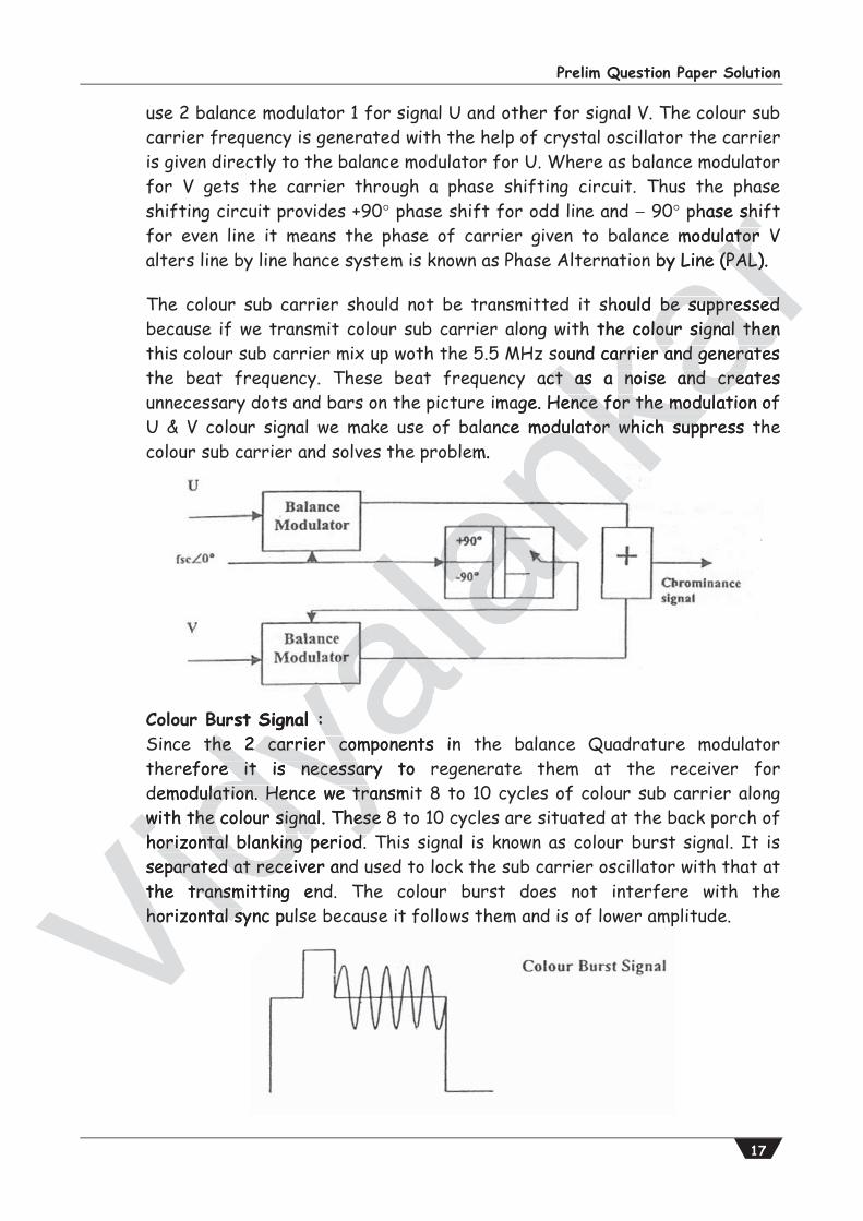
use 2 balance modulator 1 for signal U and other for signal V. The colour sub carrier frequency is generated with the help of crystal oscillator the carrier is given directly to the balance modulator for U. Where as balance modulator for V gets the carrier through a phase shifting circuit. Thus the phase shifting circuit provides +90 phase shift for odd line and 90 phase shift for even line it means the phase of carrier given to balance modulator V alters line by line hance system is known as Phase Alternation by Line (PAL). The colour sub carrier should not be transmitted it should be suppressed because if we transmit colour sub carrier along with the colour signal then this colour sub carrier mix up woth the 5.5 MHz sound carrier and generates the beat frequency. These beat frequency act as a noise and creates unnecessary dots and bars on the picture image. Hence for the modulation of U & V colour signal we make use of balance modulator which suppress the colour sub carrier and solves the problem.
Colour Burst Signal : Since the 2 carrier components in the balance Quadrature modulator therefore it is necessary to regenerate them at the receiver for demodulation. Hence we transmit 8 to 10 cycles of colour sub carrier along with the colour signal. These 8 to 10 cycles are situated at the back porch of horizontal blanking period. This signal is known as colour burst signal. It is separated at receiver and used to lock the sub carrier oscillator with that at the transmitting end. The colour burst does not interfere with the horizontal sync pulse because it follows them and is of lower amplitude.
Vidy
alank
ar
e phase sh sh
modulator V lator n by Line (PAL). (PAL)
should be suppressed be suppressed h the colour signal then lour signal then
ound carrier and generates arrier and generate act as a noise and creates ct as a noise and crea
age. Hence for the modulation ofence for the modulaance modulator which suppress tmodulator which sup
em.
urst Signal : : the 2 carrier components in the 2 carrier co
erefore it is necessary to re it is necessademodulation. Hence we transmiulation. Hence we trawith the colour signal. These 8with the colour signal. Thesehorizontal blanking period. horizontal blanking period. separated at receiver anparated at recethe transmitting enthe transmhorizontal sync pulshorizontal sy

Vidyalankar : T.Y. Diploma AVE
18
Q.3(b) Explain working of LNBC with help of block diagram. [4](A) LNBC
The main function of the LNBC is to convert collected signal to a low frequency range to minimize losses in co-axial cable that carry dish antenna signals to control room.
The figure shows block diagram of LNBC or also called front end converter. The composite signal collected by the feed horn is fed to a Low Noise
Amplifier (LNA) which provides enough gain while maintaining maximum possible signal-to-noise ratio.
The LNA output fed to a converter which converts the incoming microwave (high frequency) signals to a lower frequency range.
This is done using local oscillator frequency of converter. A Band Pass Filter (BPF) at the output of mixer separates the wanted
I.F. signals from other signals. These signals are amplified by multistage I.F. amplifier and then sent to
co-axial cable to the control room (or cable station). It is necessary to install 2, 4, 6 or 8 dish antenna units with feed-horn
and LNBC to collect signals from different satellites.
Fig.: Block diagram of an LNBC.
Specifications of LNBC : i) Input frequency 3.625 to 4.2 GHz ii) Output frequency 950 to 1525 MHz iii) Local oscillator frequency 5150 MHz. iv) Impedance 75
Vidy
alank
arrrar
erter.
ar
o a Low Noise
karaining maximum
kaka
ch converts the incom
ka frequency range.
nka onverter.
nkf mixer separates t
nkankge I.F. amplifier
an or cable statan 6 or 8 dish antenn
lannals from different satellla
Vidy
Vid
ViVSpeVi) IV) V
iv) I

Prelim Question Paper Solution
19
Q.3(c) Compare Addictive and subtractive mixing in color TV. [4](A) Subtractive Mixing A sensation of colour is produced by opaque objects or materials when white
light falls on them. It is so because any surface does not reflect all the wave lengths of the incident light uniformly. In fact, only some out of these are reflected and the rest get absorbed at the surface of the object. Thus any object is seen in a colour corresponding to the spectrum of radiated light which is not absorbed but instead gets reflected. For example, A red apple absorbs light of all colours except red which it reflects and thus looks red based on such facts special chemical called pigments are used for printing and painting. A yellow pigments absorbs violet, blue, green, orange and red but reflects the remaining yellow. When pigments of two or more colours are mixed they reflects wavelength of only those colours which are common to both and these combine to give the sensation of a new colour. Making colours by mixing paint pigments is therefore described as “subtractive mixing”. Since each added pigment subtracts more from white light and leaves less to be reflected to the eye. Additive Mixing This is another method to produce various colours. When light of two or more different colours are mixed and projected on a white screen, the eye perceives it as a combined colour. In effect the light reflected from the screen seems to the eye as if it is coming from a new source of light which is different from any of the sources actually projected. A white colour is perceived by additive mixing sensations from all the three sets of cones two or more colours obtained either from independent sources or through filters can create a combined sensation of different colour. These (different) colours are created by mixing pure colours and not by subtracting parts from white. This method is normally used in T.Vs.
Magenta
Red
Blue
Green
Yellow
Cyan
Black
Magenta
Red
Blue
Green
Yellow
Cyan
White
59%
30%
41%
11%
70% 100%
89
Vidy
alank
ar
t aut of the the
object. Thus t. Thrum of radiated radiate
For example, A red xample, A red eflects and thus looks s and thus looks
pigments are used for nts are used fors violet, blue, green, orange s violet, blue, green, oran
When pigments of two or more en pigments of two or m of only those colours which arey those colours w
e the sensation of a new colour. sensation of a new c
ents is btractive
ed pigment gment hite light and hite light and
ed to the eye. to the eye.
method to produce various to produce variouhen light of two or more ght of two or m
colours are mixed and projected re mixed and prte screen, the eye perceives it aste screen, the eye perceive
ned colour. ed colour. In effect the In eflected from the screen seems to d from the screen s
as if it is coming from a new sour t is coming from a new which is different from any owhich is different from any oactually projected. A wctually projectedperceived by additive ceived by adfrom all the three sfrom all thmore colours omore coloindependent souindepcreate a comcreatcolour. T
an
createdubt
nanMagentanRed Red
Blue
Y

Vidyalankar : T.Y. Diploma AVE
20
Q.3(d) List the types of Amplifiers used in cable TV and give their use. [4](A) Amplifier
Amplifier increases strength of the input signal. In cable distribution system, the starting point for cable signals is called
the head end. Here, cable TV company receives programming via. satellite transmission,
micro wave transmission and local broadcast. Those signals are amplified adjusted for level and fed into the trunk
lines.
Fig.1(a) : Basic Distribution System for Cable Television.
Fig.1(b) : Trunk Amplifiers Correct for Losses in Cable Run.
Trunk Amplifiers : The trunk amplifiers are inserted at regular intervals along the trunk
route to make up for cable losses. Figure 1 shows 20-dB amplifier is at the end of a cable run with a loss of 20 dB.
The decibel unit used for cable signals is dB mV which means 'decibels above 1 mV.
Amplifiers are placed at regular intervals to keep the signal up to the standard level of 1-3 mV.
Vidy
alank
arrr
missio
arar
to the trunk
kar
kar
ka
alaic Distribution SyalidVidyFig.1(b) : Trunk Am
Vidy
Vidnk Amplifier
Vid The tru
ViVtV TVV

Prelim Question Paper Solution
21
Bridging Amplifier : A bridging amplifier is for a branch from the main trunk to feed a
particular neighbourhood in the cable system. The typical gain is 20-40 dB. The output is for the branch lines to individual subscribers. In many cases the trunk and bridging amplifiers are located in the same
weatherproof housing. An additional attenuator may be used at the input to the bridging amplifier
to balance the signal levels.
Line Amplifiers : Long line runs from the bridging amplifier may require that line extender
amplifiers be inserted in the branch line to make up for cable losses in that branch.
Such an amplifier extends the number of drop lines that can be used on branch line. The typical gain for a line amplifier is 20-40 dB.
Specifications : (i) Frequency response - 45 to 550 MHz. (ii) Gain - 40 dB, (iii) Noise - 7 dB. (iv) Input/Output impedance - 75 .
Q.3(e) What is the advantage of flourscent display in CD player? [4](A) Advantages of Fluorescent display system used in C.D. player :
Vacuum Fluorescent Display (VFD) is a display device used commonly in CD, VCD and DVDE players.
Advantages of Fluorescent Display : (i) Emits a very bright light with clear contrast. (ii) Easily support display elements of various colours. (iii) The light produced by most VFDs contain many colours and can often be
filtered to produce a more pure colour such as deep green or deep blue. (iv) Being rugged, inexpensive. (v) Easily configured to display a wide variety of customized messages. (vi) Most VFDs continue to function normally in sub-zero temperatures
making them ideal for outdoor devices in cold climates.
Vidy
alank
arrr
e sam
arar
ging amplifier
kar
kar
kakaay require that line extekaake up for cable
nknk drop lines that cnk mplifier is 20-40ananlan 5 to 550 MHz. laala
alaance - 7
advantage of flourscent displaytage of flourscent s of Fluorescent display systemorescent display
dya Fluorescent Display (VFD
dyad DVDE players.
dydytages of Fluorescent
idy(i) Emits a very bright ligh
Vidyi) Easily support
Vid) The light pro
Vidltered
Vi(iv) Being rV(v) V(vi) V

Vidyalankar : T.Y. Diploma AVE
22
Q.4(a) Attempt any TWO of the following : [12]Q.4(a) (i) Explain CCTV. [6](A) Closed Circuit Television (CCTV)
As the name implies, it is a system in which the circuit is closed and all elements are directly connected.
This is unlike broadcast television where any receiver that is correctly tuned can pick up the signal-from the airwaves.
In the Closed Circuit Television (CCTV) system the video output from a TV camera is fed directly by a co-axial or a low power wireless link to a special type of TV receiver called a monitor which is installed at a remote position so that the picture is produced on the screen of the monitor.
A TV monitor or a video monitor is as ordinary TV receiver without the RF-IF stages.
It produces the picture directly from the composite video signal supplied by TV camera.
When a number of cameras are used for monitoring at different locations, a camera selector switch is used to select the signals from different cameras.
CCTV is a very useful system which finds many applications in education, industry, business, medicine and traffic control.
Simple CCTV System The simplest system is a camera connected directly to a monitor by a
coaxial cable with the power for the camera being provided from the monitor. This is known as line powered camera.
The next development was to incorporate the outputs from four cameras into the monitor.
These could be set to sequence automatically through the camera. There was even a microphone built into the camera to carry sound and a
speaker in the monitor.
Fig.1(a): A Basic Line Powered CCTV System.
Vidy
alank
arrr
rrect
arar
utput from a
karreless link to a
kar is installed at a
ka
uced on the screen of t
kaka TV receiver wit
nknk composite video nkan used for monitoanitch is used to s
lanlaystem which finds many
alae and traffic con
alaalya
stem is a camera co
ya
ith the power fo
dyaitor. This is known as line p
dyae next development
dy
ras into the monito
dyese could be set to se
idy There was even a microp
Vidyspeaker in the
Vid

Prelim Question Paper Solution
23
Fig.1(b) : A Four-Camera Line Powered CCTV System.
Movable Camera
Fig.1(c): Multiple Camera System.
All the cameras shown above are fixed with fixed focal length lenses. In many applications the area to be covered would need many fixed
cameras. The solution to this is to use cameras fixed to a movable platform.
This platform then be controlled from a remote location. Cameras may be used indoors or outdoors. Some systems may contain a combination of both fixed and movable
cameras shown in figure through switcher and controller.
Vidy
alank
arkar
nkred CCTV System. anan
Vid
Vid
Vid
Vi All the cV VcVVV

Vidyalankar : T.Y. Diploma AVE
24
Fig.: Block Diagram of a CD Player
Applications of CCTV (i) Monitoring traffic on a road (or bridge). (ii) At cricket or football stadiums. (iii) Production control in factory. (iv) In hospitals, important surgical operations can be shown to students
outside the operation theatre and also a watch can be kept on patients in bed.
(v) Police can use CCTV for traffic control and control of crime and in banks. (vi) In business houses the CCTV is helpful in observing customers and sales
people from remote positions. Q.4(a) (ii) Draw the block diagram of Audio CD player. [6](A) CD Player
CLV v/s CAV The CD player is known as a CLV or “Constant Linear Velocity” system.
In a CLV device such as the CD player the rotational speed of the disc player is adjusted with the movement of the reading mechanism on the disc
Vidy
alank
arr
den
rients
arar
and in banks.
karomers and sales
kar
yer. r. [6]
VV

Prelim Question Paper Solution
25
surface. This speed is changed to maintain a constant linear velocity, i.e. the signal on the disc surface always moves at a constant speed of 1.3m per second under the pickup head.
Half-Full Memory This half-full memory circuit makes the disc to maintain a constant linear velocity when the reading mechanism moves from outer tracks of the disc to the inner tracks or from inner tracks to the outer tracks on the disc surface. This half-full memory is always maintained at a half-full position and the reading mechanism will remove signal from this memory and process the audio signals without showing any effect of the disc speed change. Also the clock signal, which is stored on the CD surface with the data, is used to maintain a constant linear velocity of the CD play.
Decoding CD During the decoding, the digital data on the disc surface is read by the decoding circuit and is converted into the analog audio signal required to drive the speakers and to re-generate the stored music.
Optical Pick-up The audio signals stored on the CD surface as pits and flat areas arc first picked up by the optical pick-up made of lens assembly, prism, photo detectors and laser diode assembly in the Optical Pickup unit.
High-Frequency Amplifier This signal is very weak so it is amplified by a high-frequency RF-Amplifier circuit to bring the signal to a proper level. This amplified and filtered high-frequency (HF) signal contains audio signal as well as synchronization signals in 14 bit EFM (Eight to Fourteen Modulated) format, this signal is sent to an EFM demodulator circuit.
EFM Demodulator The EFM demodulator separates the modulated data and the timing
signal from the signal received at its input. It also removes the additional coupling bits and convert the 14 bit EFM symbol to actual 8 bit data.
The amplified and filtered EFM signal from the High-Frequency amplifier is also given to the clock regeneration circuit and to the synchronization detecting and timing circuit. These circuits are used to recover the bit clock and the sync pattern from the data. The timing signal separated by this circuit is used to provide timing signal to the system.
Vidy
alank
arrr
t line
ar
disc t
ar
on the disc
karalf-full position
ka
emory and process
ka
the disc speed change. A
kaace with the data, is use
nka
nknkan the disc surfacan
to the analog ante the stored mus
lanlaala CD surface as
alacal pick-up madalde assembly in the
yayamplif
dyagnal is very weak so it is
dya
to bring the signal
dyncy (HF) signal conta
idy
bit EFM (Eight to Four
VidyEFM demodulator circuit.
Vidy
VidM Demodulat
Vid
The EFM
ViVaVdVV

Vidyalankar : T.Y. Diploma AVE
26
ERGO Circuit Demodulated data from the EFM demodulator is send to an error correction (ERCO) circuit. This demodulated data signal is also send to control and display decoding circuit, which recovers the control and display signals multiplexed into the signal received from the CD.
Interpolation and Muting This ERCO circuit is mainly used for the task of error detection and correction purpose. Any error found in the incoming data signal is send to the interpolation and muting section by the ERCO circuit. This information is sent with a flag signal indicating the type of action to he performed to correct the error.
The interpolation and muting section uses the following methods to correct any error found in the data stream read from the disc. Muting Last Word held Linear interpolation
Muting In muting, when an error is detected in the data stream, the player will mute (silence) the sound output so that the undesirable sound is not send to the speaker.
Previous Word Held When the analog signal is sampled, each sample is given a 16 bit word value. A 16 bit word can have 65,536 different values. Normally an audio signal is a smooth analog wave, so if any data is missing from the data stream read from the disc, it can be assumed that the missing data will be about only l/65536th different from its previous word. A difference of only 1/65526 is such a small difference that no human being can detect it. So, in this method of “Previous Word Held”, the missing data in a sound stream is filled with the data from the previous word in the stream.
Vidy
alank
arrrarar
etection and
kargnal is send to
kar This information is
ka
action to he performed
kakank following methods t
nk the disc. nkananlanlaalaected in the dat
alaut so that the undes
alyaya
d
dya he analog signal is sampled
dya word can have 65,5
dy
analog wave, so if
dy the disc, it can be as
idyl/65536th different from it
Vidyuch a small differ
Vid “Previous Wor
Vidthe data fro
Prelim Question Paper Solution
27
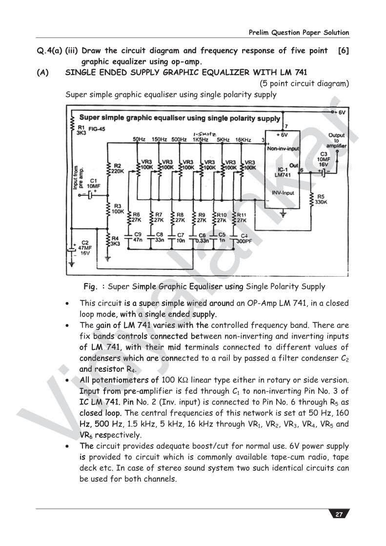
Q.4(a) (iii) Draw the circuit diagram and frequency response of five pointgraphic equalizer using op-amp.
[6]
(A) SINGLE ENDED SUPPLY GRAPHIC EQUALIZER WITH LM 741 (5 point circuit diagram)
Super simple graphic equaliser using single polarity supply
This circuit is a super simple wired around an OP-Amp LM 741, in a closed loop mode, with a single ended supply.
The gain of LM 741 varies with the controlled frequency band. There are fix bands controls connected between non-inverting and inverting inputs of LM 741, with their mid terminals connected to different values of condensers which are connected to a rail by passed a filter condenser C2 and resistor R4.
All potentiometers of 100 K linear type either in rotary or side version. Input from pre-amplifier is fed through C1 to non-inverting Pin No. 3 of IC LM 741. Pin No. 2 (Inv. input) is connected to Pin No. 6 through R5 as closed loop. The central frequencies of this network is set at 50 Hz, 160 Hz, 500 Hz, 1.5 kHz, 5 kHz, 16 kHz through VR1, VR2, VR3, VR4, VR5 and VR6 respectively.
The circuit provides adequate boost/cut for normal use. 6V power supply is provided to circuit which is commonly available tape-cum radio, tape deck etc. In case of stereo sound system two such identical circuits can be used for both channels.
Fig. : Super Simple Graphic Equaliser using Single Polarity Supply
Vidy
aluit is a super simple wired around super simple wired ode, with a single ended supply. a single ended s
gain of LM 741 varies with the c gain of LM 741 varies witix bands controls connected bet bands controls con
of LM 741, with their mid teM 741, with their condensers which are connendensers which are coand resistor Rd resistor R44. .
All potentiometers of All potentiometInput from pre-ampInput from pIC LM 741. Pin N LM 7closed loop. Thd lHz, 500 HzVRV 6 resp
The cis p
alank
ar
dia
Simple Graphic Equaliser using Se Graphic Equalise

Vidyalankar : T.Y. Diploma AVE
28
Q.4(b) Attempt any ONE of the following : [6]Q.4(b) (i) Explain the circuit of color killer circuit. [6](A) Ident and Colour Killer Circuit :
The main function of this circuit is to amplify burst phase ident signal and to generate colour killer bias voltage.
A shown in the circuit diagram, transistor Q9 is tuned collector amplifier whose collector is tuned to 7.8 kHz frequency. Thus, square waveform of frequency 7.8 kHz obtained at the output of phase discriminator is amplified by Q9. The R59 and R«) provides voltage divider biasing to Q9 whereas R61 is a emitter resistance used td stabilize Q pt of Q9. Thus after amplification we get 3.5Vp-p signal at the final output.
(a) Colour Killer: The centre tapped inductor L4 at the collector of Q9 works as an autotransfortwer and generates 25Vp-p signal at collector of Q9. This signal is given to diode D10 and capacitor C30. They work as a half wave rectifier with C filter and provides a steady DC level of about 13.5V. Thus whenever the TV receives the composite video signal of colour picture than we get 7.8 kHz signal due to which we get 13.5V steady sDC level. This DC level is given to second chroma band pass amplifier and because of this DC level, chroma band pass amplifier turns ON. On the other hand when TV receives monochrome signal then we don't have 7.83 kHz signal at base of Q9. Hence, the DC level falls to or below 2V and due to this the chroma band pass amplifier turns OFF. Thus, colour killer circuit turns OFF chroma band pass amplifier for monochrom received signal.
Vidy
alank
ar circuit is to ircuit is to amplify burst phase amplify burst
bias voltage. tage.
rcuit diagram, transistor Q diagram, transistor 9 is is tuned to 7.8 kHz frequencyed to 7.8 kHz fre
8 kHz obtained at the output of p obtained at the oute R59 and R«) provides voltage dd R«) provides v
mitter resistance used td stmitter resistance used fication we get 3.5Vp-p signal atcation we get 3.5Vp
a) Colour Killer: The centre taour Killer: The centworks as an autotransfortrks as an autotransfoof Q9. This signal is givof Q9. This signal is giva half wave rectifiea half wave rabout 13.5V. Thus bout 1of colour pictur olousteady sDC amplifier aON. Ondon'b

Prelim Question Paper Solution
29
Q.4(b) (ii) Explain with the help of circuit diagram, how EHT voltage isgenerated?
[6]
(A) EHT GENERATION Generation of EHT for Picture Tubes : In monochrome TV receiver EHT potential generating by overwind on L.O.T. but it is not possible beyond 16 kV because of problems like flash over, high impedance and poor regulation. So in colour TV to generate EHT upto 25 kV the diode split addition technique is used. It has advantages like greater reliability, small size and low cost.
Figure 1 shows the principle of Diode split addition. Three layers of secondary windings are wound on ferroxide core of the
L.O.T (Line Output Transformers). In actual practice, three sections shown separately and wound one above
the other and are thus concentric. Each winding is identical to the other and has the same number of turns
therefore same voltage induced in each section. Every time the flyback-derived input pulse gets applied to the primary
winding (not shown here). The layers are close to each other, thus inter-layer capacitance exists
between each of them (shown by dotted line). If a diode is connected between the end of one layer of winding and the
start of next, the a.c. voltages induced in each layer can be made to charge up all the inter-layer capacitance to the same voltage.
Since the capacitances are effectively in series, the total voltage appearing at the output terminal is sum of all the voltages appearing across all of them.
The three windings are so designed that voltage induced in each layer form the flyback transformer 8.33 kV. This makes total potential equal to 25 kV and forms the EHT supply source.
Anode of 37 cm (14") monochrome picture tube needs 12 kV for good brightness on screen. 51 cm (20") B/W picture tube needs 16 kV. Vi
dyala
nkarr
.O
rer, hi
ararkare split addition
karity, small size and
kakakankund on ferroxide co
nknkn separately andanan other and has the
lan induced in each sectionla-derived input pulse ge
alaala to each other, thu
alem (shown by dott
ya
nnected between th
ya
the a.c. voltage
dyarge up all the inter-layer c
dyace the capacitanc
dy
aring at the outpu
dyross all of th
idy The three windings are
Vidyform the flyba
Vidto 25 kV and
Vid
ViAnode of Vbrig

Vidyalankar : T.Y. Diploma AVE
30
Fig. 2: Simplified Line Output Circuit showing Generation of Supply Voltages Necessary for various Electrodes of a Colour Picture Tube
Fig. 1 : Principle of Split Diode Operation to obtain EHT and Focus Anode Potentials for a Colour Picture Tube.
Circuit for generating EHT :
Vidy
ala
rar
ande Operation t
ans for a Colour Pict
lan EHT : :
Prelim Question Paper Solution
31
Anode potential (G2) is obtained for screen grid separately at collector of Q2.
This is rectified by D1 and then filtered by C10. Output dc voltage is 550 to 800 V.
Any failure of G2 means no beam current and hence no spot is produced on screen.
Focus anode (G3) potential needed is 6.5 kV to 7.5 kV. It is obtained from diode split winding (D2, D3 and D4). Each stage produces potential of 8 kV.
Q.5 Attempt the following : [16]Q.5(a) Explain the Basic principle of LCD TV. [4](A) LCD It is cheaper and needs little power and so they hold maximum promise for
being used as flat panel display.
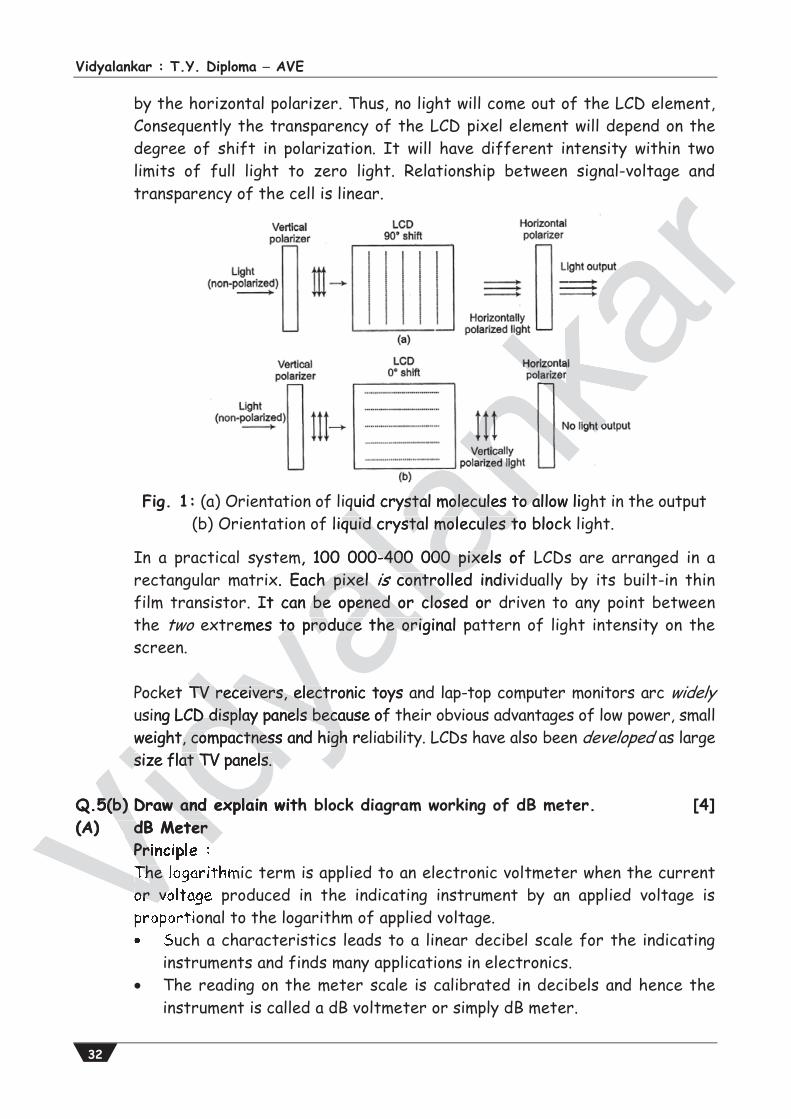
Liquid crystals are organic compounds whose physical properties are the same as those of a crystal, but whose behaviour resembles that of a liquid. Hence they are known as liquid crystals. A molecule of a liquid crystal has an elongated rod like shape and its structure is somewhat rigid. Electric conductivity, refractive index and polarization of a light coming out of it depends on the orientation of its crystals. This property of a liquid crystal is used to make the light, passing through it, change its polarization. The liquid crystals adjust themselves parallel or perpendicular to the electric field.
The electric field applied to an LCD cell twists the molecules, the twist being proportional to the signal voltage. The electric field is applied at right angles to the axes of liquid crystals. The LCD element has a thin (about 10 micron thick) liquid crystal sandwitched between two transparent plates. When the voltage applied to the plates varies, the polarization of light passing through the liquid crystal changes. It can change between 0 and 90 degree. The action of an LCD is shown in figure 1(a) and (b).
The polarization of the incident light is random. The vertical polarizer selects only vertically polarized light. In figure 1(a), the LCD crystal causes a shift of 90° in the polarization and hence it becomes horizontally polarized light. The next polarizer is the horizontal polarizer which allows this light to pass and so light comes out of the LCD element. In figure 1(b) the LCD crystal causes no shift in the polarization. So the light coming out of the liquid remains vertically polarized, which is stopped
Vidy
alank
ar
s producuc
V. It is obtained btaine produces potential ces potential
[16][[4]
so they hold maximum promise ey hold maximum pr
pounds whose physical properts whose physical put whose behaviour resembles those behaviour rese
quid crystals. A molecule of a liququid crystals. A molecule ope and its structure is somew and its structure is
ve index and polarization of a and polarizationentation of its crystals. This proon of its crystals. Th
e light, passing through it, chang passing through itst themselves parallel or perpendmselves parallel or p
ctric field applied to an LCD cell ctric field applied to an LCortional to the signal voltage. Thetional to the signal
the axes of liquid crystals. The xes of liquid crystathick) liquid crystal sandwitched liquid crystal sandwitvoltage applied to the plates voltage applied to the platesthe liquid crystal changeshe liquid crystal action of an LCD is showion of an LCD
The polarization ofThe polarizonly vertically ponly 90° in the po90° inext polarlight co
Vidyalankar : T.Y. Diploma AVE
32
by the horizontal polarizer. Thus, no light will come out of the LCD element, Consequently the transparency of the LCD pixel element will depend on the degree of shift in polarization. It will have different intensity within two limits of full light to zero light. Relationship between signal-voltage and transparency of the cell is linear.
Fig. 1: (a) Orientation of liquid crystal molecules to allow light in the output
(b) Orientation of liquid crystal molecules to block light.
In a practical system, 100 000-400 000 pixels of LCDs are arranged in a rectangular matrix. Each pixel is controlled individually by its built-in thin film transistor. It can be opened or closed or driven to any point between the two extremes to produce the original pattern of light intensity on the screen. Pocket TV receivers, electronic toys and lap-top computer monitors arc widely using LCD display panels because of their obvious advantages of low power, small weight, compactness and high reliability. LCDs have also been developed as large size flat TV panels.
Q.5(b) Draw and explain with block diagram working of dB meter. [4](A) dB Meter
Principle : The logarithmic term is applied to an electronic voltmeter when the current or voltage produced in the indicating instrument by an applied voltage is proportional to the logarithm of applied voltage. Such a characteristics leads to a linear decibel scale for the indicating
instruments and finds many applications in electronics. The reading on the meter scale is calibrated in decibels and hence the
instrument is called a dB voltmeter or simply dB meter.
Vidy
alank
ar
ag
quid crystal molecules to allow lig quid crystal molecules to a liquid crystal molecules to block quid crystal molecules t
m, 100 000-400 000 pixels of L0-400 000 pixex. Each pixel h pixel is controlled indivicontro
It can be opened or closed or be opened or closremes to produce the original pa to produce the orig
et TV receivers, electronic toys a TV receivers, electsing LCD display panels because of CD display panels beca
weight, compactness and high re, compactness and high size flat TV panels. size flat TV panels.
Q.5(b) Draw and explain with 5(b) Draw and explai(A) dB Meter dB Meter
ViPrinciple : VThe Vor voVV
Prelim Question Paper Solution
33
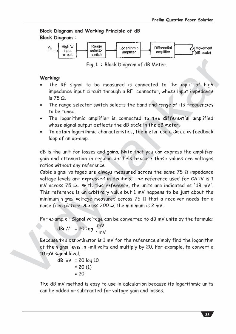
Block Diagram and Working Principle of dB Block Diagram :
Fig.1 : Block Diagram of dB Meter.
Working: The RF signal to be measured is connected to the input of high
impedance input circuit through a RF connector, whose input impedance is 75 .
The range selector switch selects the band and range of its frequencies to be tuned.
The logarithmic amplifier is connected to the differential amplified whose signal output deflects the dB scale in the dB meter.
To obtain logarithmic characteristics, the meter use a diode in feedback loop of an op-amp.
dB is the unit for losses and gains. Note that you can express the amplifier gain and attenuation in regular decibels because these values are voltages ratios without any reference. Cable signal voltages are always measured across the same 75 impedance voltage levels are expressed in decibels. The reference used for CATV is 1 mV across 75 .. With this reference, the units are indicated as 'dB mV'. This reference is an arbitrary value but 1 mV happens to be just about the minimum signal voltage measured across 75 that a receiver needs for a noise free picture. Across 300 . the minimum is 2 mV.
For example : Signal voltage can be converted to dB mV units by the formula:
dBmV = 20 1og mV1mV
Because the denominator is 1 mV for the reference simply find the logarithm of the signal level in -milivolts and multiply by 20. For example, to convert a 10 mV signal level, dB mV = 20 log 10 = 20 (1) = 20
The dB mV method is easy to use in calculation because its logarithmic units can be added or subtracted for voltage gain and losses.
Vidy
alank
arrrararkar input of high
karse input impedance
kaka and range of its frequenkank to the differential
nk in the dB meter. nk the meter use a ananlannd gains. Note that you calaular decibels because
alaalae always measured a
alessed in decibels.
ya
With this reference
ya
an arbitrary valu
dyam signal voltage measured
dya ree picture. Across
dydyxample : Signal voltage
Vidy dBmV = 20 1
ymV
Vidause the deno
Vidof the signa
Vi10 mV signaV V V

Vidyalankar : T.Y. Diploma AVE
34
1 mV 10 = 10 mV 0.5 mV = 5 mV = 14 dB mV 0 dB mV + 20 dB 6 dB = 14 dB mV (a) in milivolts (b) in dB mV units
Fig.2 : Calculation of Gain
Consider an amplifier with voltage gain of 10, driving a cable with an attenuation factor of 0.5 as shown in figure 2. In (a) the voltage gain of 10 is multiplied by the 1 mV signal input to get a 10-mV output. The cable reduces the signal level by one half thus the final output is 10 0.5 = 5 mV.
The 5 mV signal output corresponds to 14 dB mV because, dB mV = 20 log 5 = 20 (0.7) = 14
All values are indicated in dB mV. For a given, add dB mV for a loss subtract dB mV. The values in b are as follows. 0 dB mV is the input signal level of 1 mV. 20 dB is the amplifier gain 10. 6 dB mV is the cable attenuation of 0.5.
The end result for the signal level at the output is 0 + 20 - 6 = 14 dB mV.
Q.5(c) Explain why Vertical Synch Pulse is serrated? [4](A) Necessity of Serrated Pulses :
As we known that vertical sync pulse time period is 160j.isec, thus it occupies 2.5 to 3 times the horizontal line period. We purposely keep the width of vertical sync pulse more so that it is easy to distinguish the V sync pulse and H sync pulse at the receiver. As we known that the vertical sync pulse is available during the vertical re1ra.ce time and during this time even though the beam is blank we have to keep the horizontal oscillator ON for the proper synchronization. It means that during the vertical sync pulse time period of 160 sec we must make available horizontal for proper triggering of horizontal oscillator. To achieved this serrations are made in the vertical sync pulse. The serrated pulses are basically narrow slots in the vertical sync pulse at half line interval (every 32f.ise.c). The width of each slots is 4.7u.sec. during this slot the amplitude of vertical sync pulse.
Vidy
alank
arr
dB m
ararkar
kar cable with an
ka
n (a) the voltage gain of 1
ka a 10-mV output. The cka utput is 10 0.5 =
nknk mV because, nkananlanla dB mV. For a given, add
ala ollows
ala signal level of 1 mV.
aler gain 10.
yalble attenuation
yadya result for the signal level
plain why Vertical Synch Pulse why Vertical SyncNecessity of Serrated Pulses :sity of Serrated PulsAs we known that vertical As we known that verticaoccupies 2.5 to 3 times tccupies 2.5 to 3 times twidth of vertical sync pdth of vertical pulse and H sync pulspulse and Hpulse is available dpulse is avathough the beathouthe proper sythe pperiod of horizonsync

Prelim Question Paper Solution
35
Q.5(d) Explain the need of Synchronizing and Blanking pulses in TV. [4](A) Composite video signal consists :
(a) Video signals : Video signal is nothing but the actual picture information. (b) Blanking pulses : These pulses are required to make retrace invisible.
There are two types of Blanking pulses (i) Horizontal blanking pulses (ii) Vertical blanking pulses. They are used to blank horizontal and vertical blanking pulses respectively.
(c) Synchronizing pulses : These pulses are required to synchronize the scanning at transmitter end with receiver end. There are two types of synchronizing pulses. (i) Horizontal synch. pulses : They are transmitted after every line.
They are separated at the receiver end and given to the horizontal deflection coils.
(ii) Vertical Synch. pulses : They are transmitted after one field. They are also separated at the receiver end and given to the vertical deflection coil.
Q.6 Attempt any FOUR of the following : [16]Q.6(a) Give Band I and Band III Allocation for TV. [4](A) Television Broadcast Channels
Band I Lower VHF range 41 to 68 MHz Band III Upper VHF range 174 to 230 MHz Band IV UHF range 470 to 598 MHz Band V UHF range 606 to 870 MHz (Band II (88 to 108 MHz) is used for FM broadcasting)
Television Channel Allocation (CCIR) in Bands I and III
Band Channel
No. Frequency Range
Picture Carrier Frequency (MHz)
Sound Carrier Frequency (MHz)
I 1 40 47 (not used)
(41 68 MHz) 2 47 54 48.25 53.75 3 54 61 55.25 60.75 4 61 68 62.25 67.75
III 5 174 181 175.25 180.75 (174 230 MHz) 6 181 195 182.25 187.75
7 188 195 189.25 194.75 8 195 202 196.25 201.75 9 202 209 203.25 208.75
Vidy
alank
ar
nv
al blanking pulses nking pulses
quired to synchronize the to synchronize the end. There are two types of nd. There are two types
are transmitted after every linansmitted after eveiver end and given to the horiz end and given to
They are transmitted after one f ransmitted afte the receiver end and given to receiver end an
the following : owing nd III Allocation for TV. I Allocation for TV
cast Channels hannels Lower VHF range er VHF range
Upper VHF range Upper VHF range UHF range UHF range
V UHF range UHF range nd II (88 to 108 MHz) is used fo (88 to 108 MHz)
Television Channel AllocatTelevision Channel All
Band BandChannel Channel
No. idyVidyyI I
Vid
Vid
(41( 68 MHz) MViVi VV VVIVV(174 VV

Vidyalankar : T.Y. Diploma AVE
36
10 209 216 210.25 215.75 11 216 223 217.25 222.75 12 223 230 224.25 229.75
In the UHF bands while the channel width remains the same at 7 MHz, a band gap of 1 MHz is allowed between adjacent channels to prevent any mutual interference.
Q.6(b) Explain Interlace Scanning used in TV. [4](A) Interlace Scanning
In Interlace scanning alternate lines are scanned. When the beam reaches the bottom of the picture frame, it quickly returns to the top to scan those lines that were missed in the previous scanning. Thus total number of lines are divided into two groups called ‘fields’. Each field is scanned alternately. This method of scanning is known as interlaced scanning. This reduces flicker to an acceptable level since the area of the screen is covered at twice the rate.
In 625 line monochrome system, for successful interlaced scanning the 625 lines of each frame or picture are divided into sets of 312.5 lines. To achieve this the horizontal sweep oscillator is made to work at a frequency of 15625 Hz. (312.5 50 = 15625) to scan the same number of lines per frame
Fig. 1 : Principle of interlaced scanning. Note that the vertical retrace time has been assumed to be zero.
VidyIn Interlace scanning altern Interlace scanning alter
the bottom of the pictue bottom of thelines that were misselines that ware divided into tware divided This method oThis
kar
7 MHz prevent any ent a
[4][4]
flicker to anflicketwice the
In 62
Fig. 1 : . 1 : PrinciplePrNote that the vertical retrote that the vertical r

Prelim Question Paper Solution
37
(15625/25 = 625 lines). Now vertical sweep circuit is run at a frequency of 50 Hz instead of 25 Hz. First field ends in a half line and second field commences at middle of the line on the top of the target plate or screen. Now the beam is able to scan the remaining 312.5 lines during downward journey.
Note : In the American T.V. system, a field frequency of 60 was adopted i.e., instead of 50 times in India the whole frame was scanned 60 times, as the supply frequency is 60 Hz in USA. This brings the total number of lines scanned per second (525 (60/2) = 15750) lines.
Scanning period Now the duration of horizontal lines if 64 S [t = 1/f = 1/15625]. Out of which the active line period i.e., trace period is 52 S and the remaining 12 S is the blanking period. During blanking period the beam returns back to
left for next trace.
Similarly with field frequency at 50 Hz, the duration vertical trace and retrace is 20 ms (t = 1/50) out of this 20 ms. 18720 ms is used for trace and 1.280 ms is taken by vertical retrace period.
Now as horizontal sweep is continuous, during vertical retrace period i.e., when beam moves from bottom to top. During that time 20 horizontal sweep occurs and so 20 lines are scanned. Therefore, total 40 lines are blanked out.
(292.5 lines)
Fig.2 : Odd line interlaced scanning procedure.
Vidy
alamerican T.V. system, a field fre T.V. system, a of 50 times in India the whole f in India the w
y frequency is 60 Hz in USA. frequency is 60 Hanned per second (525 per second (525 (60/2) =
Scanning period Scanning period Now the duration of horizoNow the duration of horizowhich the active line perhich the active lS is the blanking per the b
left for next traceleft for nex
Similarly with Simiretrace is 2retraand 1.280
kar
ow
Now a
k ines)
g.2 : Odd line interlaced scanninOdd line interlace
Vidyalankar : T.Y. Diploma AVE
38
Q.6(c) Explain what do you mean by color TV is compatible with block andwhite TV.
[4]
(A) The basic working colour picture contents the information about brightness and the colour of the picture. We first invented the Black and White TV and then we designed colour TV. While designing the colour TV it is necessary that colour TV should be compatible with Black and White TV. It means that if we apply composite video signal of monochrome TV the colour TV should be able to produce Black and White picture from monochrome signal without any modification in receiving circuitry. When this happen we say that colour TV is compatible with Black and White TV. Similarly when we apply composite video signal of colour picture to the Black and White TV then it reproduces a picture this is known as reverse compatibility. To achieve complete compatibility the composite colour signal must meet the following requirements. 1) It should occupy same bandwidth as the monochrome signal. 2) The location of picture and sound earner frequency should remain the
same. 3) The colour signal should have same luminance information as would a
monochrome signal transmitting the same scene. 4) The deflection and sync signals should remain same as in monochrome
signal. 5) The colour signal should contain colour information together with require
signals to allow it to be decoded. 6) The colour TV signal must be decode such a way that it does not affect
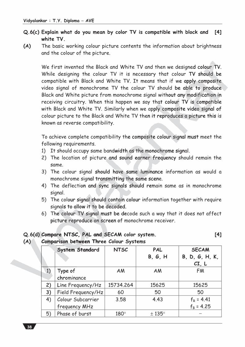
picture reproduce on screen of monochrome receiver. Q.6(d) Compare NTSC, PAL and SECAM color system. [4](A) Comparison between Three Colour Systems
System Standard NTSC PAL B, G, H
SECAM B, D, G, H, K,
CI, L 1) Type of
chrominance AM AM FM
2) Line Frequency/Hz 15734.264 15625 15625 3) Field Frequency/Hz 60 50 50 4) Colour Subcarrier
frequency MHz 3.58 4.43 fR = 4.41
fB = 4.25 5) Phase of burst 180 135
ed colour TV. our Tr TV should be ould b
we apply composite ply composite d be able to produce ble to produce
thout any modification in any modification inat colour TV is compatible at colour TV is compatib
pply composite video signal of ply composite video signaen it reproduces a picture this isproduces a pictur
he composite colour signal must posite colour sign
dwidth as the monochrome signah as the monochroe and sound earner frequency se and sound earner frequ
should have same luminance in have same lumingnal transmitting the same sceneransmitting the same
ion and sync signals should remd sync signals shou
lour signal should contain colour al should containals to allow it to be decoded. als to allow it to be decode
The colour TV signal must be dece colour TV signal mpicture reproduce on screen ofure reproduce on sc
(d) Compare NTSC, PAL and SEd) Compare NTSC, PAL and SA) Comparison between Thre) Comparison betwee
System Standar System S
Vid
ViVid
1) Type of 1) chromVVV2) LinVVV3) VVV
4

Prelim Question Paper Solution
39
6) Used in countries Canada, Colombia, Greenland, Japan, Mexico etc.
Australia, Bangladesh, Denmark, India etc.
Congo, Egypt, Iran, Iraq, Poland etc.
Q.6(e) Explain CD pick up assembly. [4](A) CD PICKUP
The optical pickup unit comes as a single unit and the complete unit need to be replaced when any problem occur to this unit. The pick-up assembly basically consist of A low power laser diode to illuminate the CD tracks Lens and prism arrangement to direct the laser beam to the CD surface
and to direct the reflected laser beam towards photo-diode array A photo-diode array to obtain data, focus and tracking signal from the
reflected laser beam Focus and Tracking coils to focus the laser beam to the CD surface and
to move the assembly to proper track across the disc surface.
Some optical units do not contain the tracking coil, for ex. the single-beam radial tracking assembly, this is explained in later sections.
Fig. 1: Single-Beam Radial Tracking Arrangement of Optical Pick-Up Unit
Vidy
alank
arr
[4][4
complete unit need to ete unit need to t. The pick-up assembly pick-up assembly
D tracks tracks the laser beam to the CD surfac beam to the CD
m towards photo-diode array ards photo-diota, focus and tracking signal frocus and tracking si
focus the laser beam to the CD the laser beam to t roper track across the disc surf track across the d
Fig.

Vidyalankar : T.Y. Diploma AVE
40
Fig.2: Optical Arrangement in a Single-Beam Radial Tracking
Pick-Up Assembly
In the optical pick-up unit, the laser diode emits laser beam from a small point into an elliptical or conical distribution. This beam is passed through various prism and lens to form a very small diameter light beam on the disc surface at the center of the track.
The objective lens is controlled by the tracking and focusing coil to keep the beam focused on the CD and to keep the condensed beam at the center of the track. This laser beam is reflected back by the flat area and the pits on the disc surface. This reflected beam is applied to a group of a group of photo-diodes through objective lens, collimator lens, and some prism arrangement.
These photo-diodes induce voltage according to the reflected beam falling on it. Focus error and tracking error voltage generated by this photo-diode array is applied to the tracking and focusing coil to control the objective lens and data signal generated by this photo-diode array is sent to an amplifier to amplify the data signals picked up from the disc. Finally the output from the amplifier is processed to produce the audio signal stored on the disc surface.
In a CD player the following type of optical assemblies are used. Single-beam radial tracking, Single-beam linear/straight line tracking, Three-beam linear/straight line tracking.
Vidy
alank
arduce
o the o ing on it. on it
racking error rror ated by this by this
array is applied to s applied to king and focusing coil d focusing coil
trol the objective lens objective lens data signal generated by data signal generated by
his photo-diode array is sent s photo-diode arrato an amplifier to amplify the n amplifier to ampdata signals picked up frta signals picked up the disc. Finally the oe disc. Finally the from the ampliffrom the processed to proprocessed taudio signal storedio sigsurface. ce
In a CD playeIn a C Single Sin

![ACOUSTIC UNITS FOR WALL AND CEILING · Suspension height Equivalent sound absorption area per canopy in Aobj [m²] mm 125 Hz 250 Hz 500 Hz 1000 Hz 2000 Hz 4000 Hz Knauf Cleaneo Single](https://img.pdfslide.us/doc/110x75/60804a8951ffa625d86329d0/acoustic-units-for-wall-and-ceiling-suspension-height-equivalent-sound-absorption.jpg)