Embed Size (px)
Citation preview
TRANSISTORAUDIO AMPLIFIER
MANUALby
Clive Sinclair
111
4E0
32 practical transistor amplifier circuits.
Complete parts list and full constructionaldetails.
Amplifiers ranging from 50 micro -watts75 watts output.
33 layout and constructional diagrams.
Comprehensive servicing data.
Practical hints and tips on construction.
up to
Amplifiers for hearing aids, pocket radio sets,tape recorders, record players, tableradios, etc.
Choice of amr piers for specific requirement.
High fidelity amplifier design.
Servicing and fault finding, etc.
BERNARD'S RADIO MANUALS
TRANSISTORAUDIO
AMPLIFIERMANUAL
byCLIVE SINCLAIR
BERNARDS (PUBLISHERS) LTD.THE GRAMPIANSWESTERN GATE
LONDON W.6
FIRST PUBLISHED FEBRUARY, 1962
Reprinted July, 1963.
Reprinted November, 1964.
Reprinted August, 1966.
Reprinted January, 1969.
Reprinted July, 1970.Reprinted May, 1972.
16. IP) 4.11 NIAACKNOWLEDGEMENT
We must express our grateful thanks to G.E.C.Limited, Mullard Limited, Newmarket, Limited,and the University of Cincinnati for their kindco-operation in supplying us with informationwithout which this book would not have beenpossible.
We invite all authors, whether new or well established, to submit manuscriptsfor publication. The manuscripts may deal with any facet of electronics but shouldalways be practical. Any circuit diagrams that may be included should have beenthoroughly checked by the author. If you are considering trying your hand atwriting this type of book we suggest that you let us have a short summary of thesubject you intend to cover. We will then be able to let you know the size of bookrequired and perhaps give you some advice on presentation.
© 1962
Printed by V. Cooper & Partners Ltd., Flitcroft Street, W.C.2,for Bemards (Publishers) Ltd., The Grampians, Western Gate, London, W.6.
CONTENTS
Page
Chapter 1. Amplifiers with outputs of up to 10mW 6
Chapter 2. Amplifiers with outputs between 10 and 100mW 13
Chapter 3. Amplifiers with outputs between 100mW and 1 Watt 17
Chapter 4. Amplifiers with outputs between 1 Watt and 75 Watts 29
LIST OP ILLUSTRATIONS
Page
Fig. 1. 500 microwatt output amplifier 7
Fig. 2. Direct coupled milliwatt amplifier 7
Fig. 3. A 2 mW direct coupled amplifier 9
Fig. 4. 5 milliwatt amplifier 9
Fig. 5. Direct coupled amplifier with low battery drain 10
Fig. 6. 6 milliwatt direct -coupled amplifier 10
Fig. 7. Complementary symmetry push-pull amplifier 12
Fig. 8. 1.5 milliwatt amplifier for use with a crystal earpiece 12
Fig. 9. 20 mW class A amplifier 14
Fig. 10. Direct coupled 30 mW amplifier 14
Fig. 11. Conventional 50 mW amplifier 16
Fig. 12. Simple 60 mW gramophone amplifier 16
Fig. 13. Simple 90 mW amplifier 18
Fig, 14. Direct coupled 75 mW amplifier 18
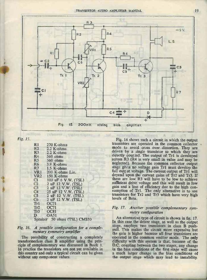
Fig. 15. 200 mW sliding bias amplifier 19
Fig. 16. A possible configuration for a complementary symmetry configuration 20
Fig. 17. Another possible complementary symmetry configuration 20
Fig. 18. G.E.C. 250 mW amplifier with symmetrical output 21
Fig. 19. G.E.C. 250 mW amplifier with transformerless output 23
Fig. 20. G.E.C. 500 mW amplifier - 25
Fig. 21. G.E.C. high stability 850 mW amplifier 26
Fig. 22. Newmarket 750 mW class A amplifier 27
Fig. 23. Milliard 540 mW amplifier 28
Fig. 24. G.E.C. transformerless output 1 watt amplifier 29
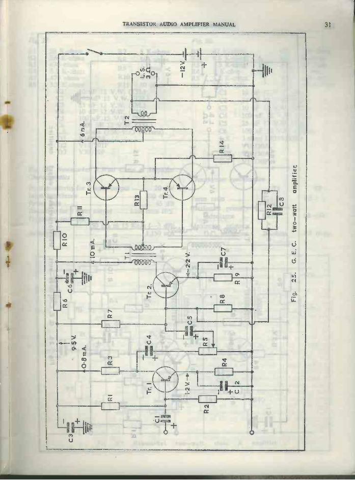
Fig. 25. G.E.C. 2 watt amplifier 31
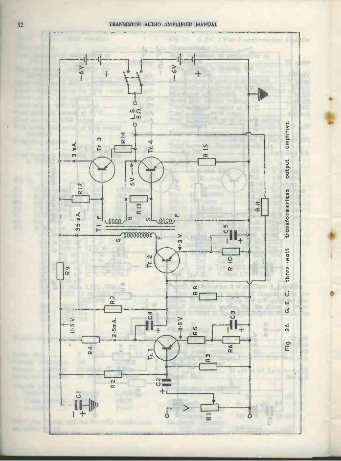
Fig. 26. G.E.C. 3 watt transformerless amplifier 32
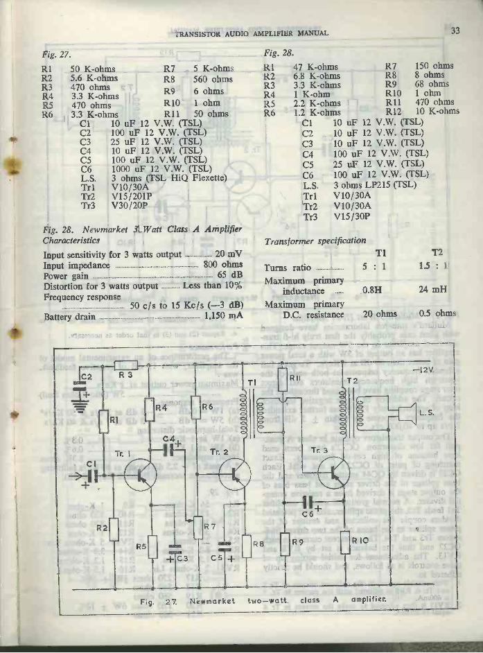
Fig. 27. Newmarket 2 watt class A amplifier 33
Fig, 28. Newmarket 3 watt class A amplifier 34
Fig. 29. Mullard 5 watt hi-fi amplifier 35
Fig. 30. Pre -amplifier stages of 15 watt public address amplifier 37
Fig. 30a. Driver and output stage of 15 watt P.A. amplifier 37
Fig. 31. Newmarket 20 watt power amplifier 39
Fig. 32. 75 watt audio amplifier 40
INTRODUCTION
In Book 1 of " Practical Transistor AudioAmplifiers " I dealt with the basic principlesinvolved in transistor A.F. amplifier design andthe practical examples given were mainly limitedto single stages. In this second book the situationis reversed and all the space is devoted to practicalamplifier circuits employing all the principles andideas already described. Most of the circuits maybe built as they stand but in a few cases thetransistors required are not yet available. Theselast mentioned circuits have been included, how-ever, for the sake of completeness and so that thebook will not be out of date for a long while tocome.
Because the range of amplifier sizes used is verywide, from a few hundred microwatts to manywatts, the book has been divided into sectionsclassified according to the power of the amplifiersdescribed. The sections cover amplifiers of from0 - 10 mW, 10 - 100 mW, 100 mW - 1 W and
1-75 W. Amplifiers that could fall into either oftwo sections are included in the latter. Forexample, a 100 mW amplifier would appear inthe 100 mW to 1 W section and not in the previousone.
Since this book leads on from the last one,the technical details given there are not repeatedhere except where an unusual application of acircuit is described or where the circuit itself isunusual. Most of the text is devoted to perform-ance specifications of the amplifiers and theircomponent values.
I have included as many amplifiers as spacewould allow but there has had to be quite a lot ofselection. Because most readers will be mainlyconcerned with the medium and low power ampli-fiers these have been given more space than thosein the high power section which are of the publicaddress size.
TSL-Ducati CapacitorsThese capacitors are specially designed for use
in transistor amplifiers. They have very long lifeand very low leakage characteristics which remainstable after years of use. Furthermore because oftheir extremely low price, the cost of any equip-ment mentioned in this book is brought down toan economical figure.
Also recommended are the TSL transistorholders, miniature loudspeakers, and all otheritems in the subminiature and miniature range ofcomponents.
SPECIAL NOTE-Polarity of input capacitor.The polarity of the input capacitor on any
amplifier in this book will depend on the natureof the signal source. With a magnetic microphonethe negative side of the electrolytic should go tothe transistor but when a transistor tuner unit isproviding the signal the base side of the capacitorshould normally be positive.
6 TRANSISTOR AUDIO AMPLIFIER MANUAL
CHAPTER 1
Amplifiers with outputs of up to 10 mW.
The first transistor amplifiers were, of course,in the very low power range and it is in this fieldthat the transistor has scored its greatest victorybecause valves, at these powers, are hopelesslyinefficient. Even the subminiature hearing aidvalves were comparative gluttons for power.
With output powers of less than 10 mW it is notnormally possible to obtain satisfactory perform-ance on a loudspeaker although, with a large andsensitive type the output can be surprising. Ampli-fiers in this range will be used mainly withearpieces therefore and are useful in hearing aidsand tiny earpiece radio sets. The quality of repro-duction obtained from a good earpiece driven bya carefully designed amplifier can be quiteremarkably good and certainly very much betterthan that obtained from a small loudspeaker.When the linkage between the diaphragm of theearpiece and the ear drum is air tight the bassresponse can be excellent and the power require-ments of the earpiece are extremely low. Thehigh sensitivity type of earpiece used with hearingaids requires a peak input of only 1 mW for a goodlistening level and the lower sensitivity types usedwith radios require up to about 10 mW depend-ing on the design.
Amplifiers for hearing aids and small radioshave to operate from extremely small batteries. Ifthe battery of such a unit is to have a reasonablelife the design must be efficient and the earpiecemust match the output impedance. It is alsoimportant that the amplifier chosen for a parti-cular application be no more than what is requiredas regards output power because the output stageis normally class A and if the amplifier is designedfor a larger output than is required there will bean unnecessary drain on the battery.
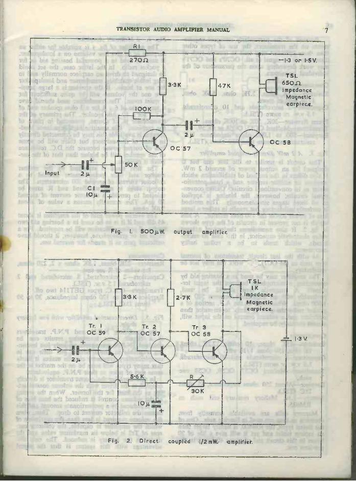
Fig. 1. 500 Microwatt output amplifier
When an earpiece of the type used in hearingaids is employed a really satisfactory sound levelcan be obtained with an A.F. drive power of onlya few hundred microwatts. This amplifier providesan output of mW which is more than sufficientfor people with normal hearing and is even enoughfor many deaf people.
The overall power gain of the amplifier is about50 dB or 100,000 times. This makes it quite suit-able as the A.F. section of a small radio or forthe output stage of a hearing aid.
When the amplifier is powered by a mercurycell such as the RM625, R1 and Cl may beomitted since no unwanted feedback will occur.The life of this cell in the circuit will be over 100hours despite its small size.
The total current consumption is 21 mA, thecurrent in the output stage being 2 mA with afresh battery.
The stabilisation in the first stage is by means ofa feedback resistor. Although this results in someA.C. feedback, the loss of gain is very slight.The output stage is not stabilised at all but theratio of the collector current to the leakage currentis large and any change in the latter will havelittle effect.
The earpiece should have an impedance of600 ohms and a D.C. resistance of between 200and 250 ohms. The Fortiphone type T earpieceis suitable.
ComponentsResistors -270 ohms, 100K ohms, 3.3K ohms,
47K ohms all 1/10th watt.Capacitors -2 microfarad, 3 v.w. x 2. 10 micro -
farad 3 v.w. (TSL).Transistors-Mullard 0057 and 0058 hearing
aid types.Volume Control- 50K ohms log or semi -log.Earpiece -600 to 650 ohms impedance. 200 to 250
ohms D.C. (TSL).Battery -1.3 volt mercury cell or 1.5 volt zinc
carbon cell.
Fig. 2. Direct Coupled milliwatt AmplifierAs was shown in Book 1, a considerable saving
in components can be achieved by the use ofdirect coupling between the transistors. Althoughthis amplifier has one more stage than the lastit uses one less resistor and one less capacitor.The power gain is about 75 dB.
The currents of the various stages should beabout 1/3 mA for Tr 1 and Tr2 and about 2 mAfor T3. Because the gains of transistors vary, it isnecessary to adjust the 30K ohm preset. resistor(which may also be 50 or 100K), . he correctcurrent in the output stage. Once correctvalue for R has been found it may be replaced bya fixed resistor of the same value.
The operation of the circuit depends upon thefact that with these types of transistor high gaincan be obtained at very low levels of collectorvoltage. The collector voltages of Trl and Tr2are in fact the same as the base voltages of Tr2and Tr3. This would normally mean that Tr 1 andTr2 where operated below their knee voltages butby employing very low collector current levels inthe first two stages this is avoided.
The battery must be a mercury cell since thehigher internal resistance of a zinc -carbon cell islikely to cause motor -boat oscillation.
TRANSISTOR AUDIO AMPLIFIER MANUAL 7
> IIInput 2 1.1,
CI10p.
RI
270 fl
33K
100K
4F-2p.
1)1 OC 57
50 K
47K
-1.3 or 1.5V.
TSL
4I 65011impedance
Magneticearpiece.
OC 58
Fig. I. 500p,W. output amplifier.
Tr. I
OC 59
> I2p,
33 K 2.7K
Tr. 2 Tr 304... 57 OC 58
10 j.-
TSLIK
impedanceMagneticearpiece.
- 1.3 V.
Fig. 2. Direct coupled 1/2 mW. amplifier.
8 TRANSISTOR AUDIO AMPLIFIER MANUAL
Because of the particularly stringent require-ments on the transistors, the use of types otherthan those specified may lead to trouble such asdistortion or no signal at all. 0070's and 0071'smay work depending upon the parameters of theindividual transistors.
ComponentsResistors -3.3K ohm, 2.7K ohm, 5.6K ohm,
1/10 watt or more.Capacitors -2 microfarads and 10 microfarads.
1.5 v.w. or more (TSL).Preset Resistor -30K, 50K or 100K ohms.Transistors-Mullard 0057, 0058 or 0059.Earpiece -500 to 1,000 ohms impedance D.C.
resistance not more than 350 ohms (TSL).
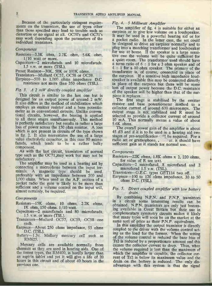
Fig. 3. A 2 mW directly coupled amplifierThis circuit is similar to the last one but is
designed for an output power of around 2 mW.It also differs in the method of stabilisation whichemploys an emitter resistor and a base potentio-meter as in conventional circuits. Unlike conven-tional circuits, however, the biasing is appliedto all three stages simultaneously. This methodis perfectly satisfactory but results in rather a largeloss of power across the 150 ohm resistor. A losswhich is not present in circuits of the type shownin fig. 2. It also necessitates the use of a largevalue electrolytic capacitor, in this case 80 micro -farads, which tends to be a rather bulkycomponent.
As with the last circuit, transistors of normaltype such as the 0C71,may work but may not besatisfactory.
The amplifier may be used as a hearing aid byconnecting a microphone between the input ter-minals. A magnetic type should be used,preferably with an impedance between 500 and1,000 ohms. When used as the A.F. section of apocket radio the gain is likely to be more thansufficient and a volume control on the input will,almost certainly, be required.
ComponentsResistors -15K ohms, 10 ohms, 2.2K ohms,
1K ohm, 150 ohms. 1/10 watt.Capacitors -2 microfarads and 80 microfarads,
1.5 v.w. or -more (TSL).Transistors-Mullard 0057, 0059, 0058 one
each.Earpiece-About 250 ohms impedance, 55 ohms
D.C. (TSL).Battery -1.3v. Mallory mercury cell such as
RM625.Mercury cells are available normally from
chemists as they are used in hearing aids. One ofthe tiniest types, the RM400, is hardly larger thanan aspirin tablet and yet it will give a life of 20hours in this circuit and of about 40 hours in theprevious one.
Fig. 4. 5 Milliwatt AmplifierThe amplifier of fig. 4 is suitable for either an
earpiece or to give low volume on a loudspeaker.It may be used in a powerful hearing aid or fora pocket radio. In the latter case, the set couldbe designed to drive an earpiece normally and toplug into a matching transformer and loudspeakerfor use at home. If the speaker is a large sensi-tive one the volume will be quite sufficient fora quiet room. The transformer used should havea turns ratio of 6 : 1 for a 3 ohm speaker and of4 : 1 for a 10 ohm speaker. The primary of thetransformer is, of course, connected in place ofthe earpiece. If a sensitive high impedance loud-speaker is available this may be connected directlyin place of the earpiece but there will be someloss of output power because the D.C. resistanceof the speaker will be higher than that of the ear-piece it replaces.
The first stage is stabilised by the emitterresistor and base potentiometer method to acollector current of around 600 microamps. Theoutput stage is not stabilised and R must beselected to provide a collector current of around10 mA. This normally means a value of about5.6K ohms.
The overall power gain of the amplifier is about45 dB and if it is to be used in a hearing aid twostages of pre -amplification "1 be required. For aradio set or gramophone, . ar, it should havesufficient gain as it stands tor normal use.
ComponentsResistors -22K ohms, 1.8K ohms x 2, 220 ohms,
for value of R see text.Capacitors -2 microfarad, 8 microfarad and 2
microfarad 1.5 v.w. (TSL).Transistors-G.E.C. types GET114 two off.Earpiece -100 to 120 ohms impedance, 30 to 50
ohms D.C. (TSL).
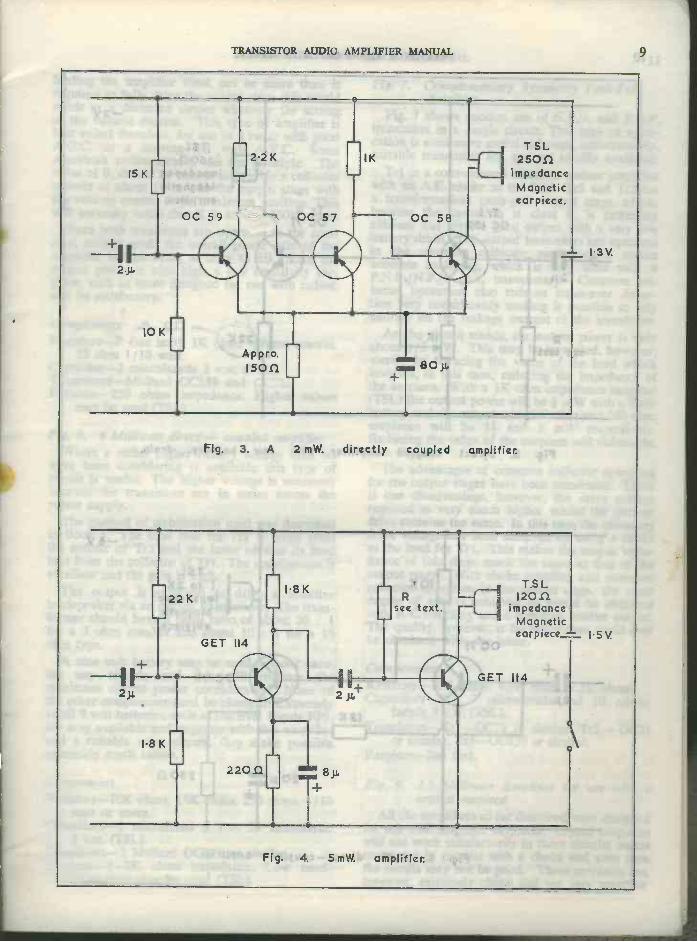
Fig. 5. Direct coupled amplifier with low batterydrain.
By combining N.P.N. and P.N.P. transistorsin a circuit some interesting results can beobtained. N.P.N. transistors are only just becom-ing available in Great Britain but their use incomplementary symmetry circuits makes it likelythat many types will soon be on the market at thesame sort of price as their P.N.P. equivalents.
In this amplifier the output transistor is directlycoupled to the driver with the volume control act-ing as the load for the former. When the settingof the volume control is reduced the base bias ofTr2 is reduced by a proportionate amount and thiscauses the collector current to drop. Thus, whenthe volume required is less than the maximum ofwhich the amplifier is capable, the collector cur-rent of Tr2 is below its maximum value and thedrain on the battery is reduced. The only dis-advantage with this system is that the signal
TRANSISTOR AUDIO AMPLIFIER MANUAL 9
15 K
OC 59
10 K
-r2.2 K
OC 57
I K
OC 58
Appro.15011 80 p.
T SL25052
impedanceMagneticearpiece.
- 1.3V.
Fig. 3. A 2 mW. directly coupled amplifier.
I2p.
22 K
GET 114
18 K
220.1
1.8K
14.2 p,
see text.
T SL41 12012
impedanceMagneticearpiece
GET 114
Fig. 4. 5 mW. amplifier.
1.5V.
10 TRANSISTOR AUDIO AMPLIFIER MANUAL
Tr. I
OC 139
Rsee ,text. -1
Tr. 2OC 71
IK
TSL25052.
impedanceMagneticearpiece.
-3V.
Fig. 5. Direct coupled amplifier with low battery drain.
OC 71
10K
IS K
TSLfl I to 2Kimpedance
Magneticearpiece.
OC 71
20 j. 25011
-6 V.
Fig. 6. 6 mW. direct-coupled amplifier.
TRANSISTOR AUDIO AMPLIFIER MANUAL 11
feeding the amplifier must not be more than isrequired to fully drive the output since this wouldresult in a distorted output whatever the settingof the volume control. This type of amplifier isbest suited therefore, for use in a radio with goodA.G.C. or a hearing aid with A.V.C. SomeAmerican radios already use the principle. Thevalue of R should be chosen to provide a collectorcurrent of about 10 mA in the output stage withthe volume control in its maximum position. Thiswill normally mean that R is around 330K ohms.
Since both transistors are operated in the com-mon emitter mode the overall power gain of theamplifier is high being at least 45 dB. Since theoutput power is also high a low sensitivity ear-piece, such as those designed for use with radios,will be satisfactory.
ComponentsResistors-R (see text), 1K ohm, volume control.
22 ohm 1/10 watt.Capacitor -2 microfarads 3 v.w. (TSL).Transistors-Mullard 0C139 and 0071.Earpiece -250 ohms impedance. Higher values
may be used (TSL).
Fig. 6. 6 Milliwatt direct - coupled amplifierWhere a rather higher battery voltage than we
have been considering is available this type ofcircuit is useful. The higher voltage is necessarybecause the transistors are in series across thepower supply.
The method of stabilisation used was describedin Book 1. The base bias for Tr 1 is taken fromthe emitter of Tr2 and the latter obtains its basebias from the collector of Tr 1. The stabilisation isexcellent and the gain is high.
The output is sufficient to drive a sensitiveloudspeaker via an output transformer. The trans-former should have a turns ratio of about 20 : 1
for a 3 ohm speaker and about 10 : 1 for a 10ohm type.
A nine volt battery may be used without caus-ing any trouble and this will increase themaximum output power considerably. None ofthe other components need be changed. Extremelysmall 9 volt batteries, such as the Ever Ready PP5,are now available and, together with this amplifierand a suitable tuner circuit, they make possibleextremely small radios.
ComponentsResistors -10K ohms, 15K ohms, 250 ohms. 1/10
watt or more.Capacitors -2 microfarad 6 v.w. 20 microfarad
3 v.w. (TSL).Transistors -2 Mullard 0071's or similar.Earpiece -1 - 2K ohms impedance. Low sensi-
tivity type may be used (TSL).
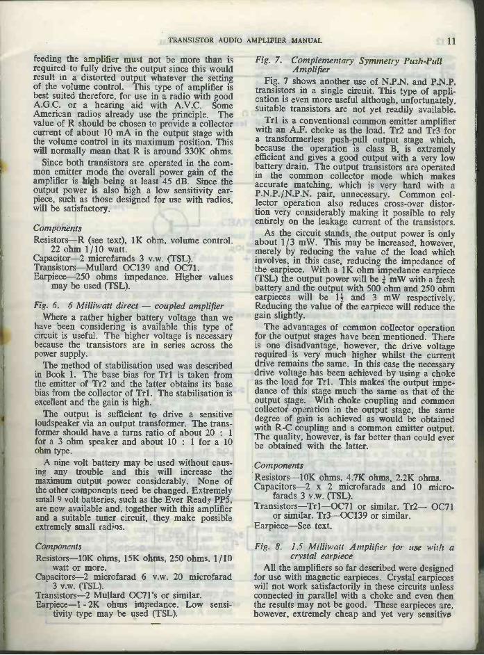
Fig. 7. Complementary Symmetry Push -PullAmplifier
Fig. 7 shows another use of N.P.N. and P.N.P.transistors in a single circuit. This type of appli-cation is even more useful although, unfortunately,suitable transistors are not yet readily available.
Trl is a conventional common emitter amplifierwith an A.F. choke as the load. Tr2 and Tr3 fora transformerless push-pull output stage which,because the operation is class B, is extremelyefficient and gives a good output with a very lowbattery drain. The output transistors are operatedin the common collector mode which makesaccurate matching, which is very hard with aP.N.P./N.P.N. pair, unnecessary. Common col-lector operation also reduces cross -over distor-tion very considerably making it possible to relyentirely on the leakage current of the transistors.
As the circuit stands, the output power is onlyabout 1/3 mW. This may be increased, however,merely by reducing the value of the load whichinvolves, in this case, reducing the impedance ofthe earpiece. With a 1K ohm impedance earpiece(TSL) the output power will be mW with a freshbattery and the output with 500 ohm and 250 ohmearpieces will be 11 and 3 mW respectively.Reducing the value of the earpiece will reduce thegain slightly.
The advantages of common collector operationfor the output stages have been mentioned. Thereis one disadvantage, however, the drive voltagerequired is very much higher whilst the currentdrive remains the same. In this case the necessarydrive voltage has been achieved by using a chokeas the load for Tr 1. This makes the output impe-dance of this stage much the same as that of theoutput stage. With choke coupling and commoncollector operation in the output stage, the samedegree of gain is achieved as would be obtainedwith R -C coupling and a common emitter output.The quality, however, is far better than could everbe obtained with the latter.
ComponentsResistors -10K ohms, 4.7K ohms, 2.2K ohms.Capacitors -2 x 2 microfarads and 10 micro -
farads 3 v.w. (TSL).Transistors-Tr 1-0071 or similar. Tr2- 0071
or similar. Tr3-0C139 or similar.Earpiece-See text.
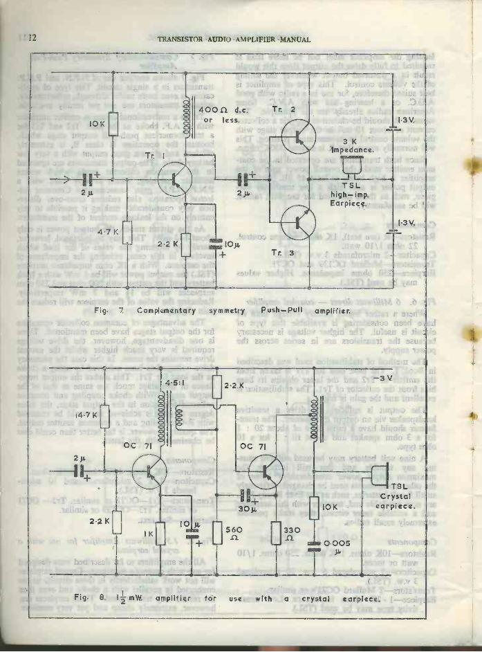
Fig. 8. 1.5 Milliwatt Amplifier for use with acrystal earpiece
All the amplifiers so far described were designedfor use with magnetic earpieces. Crystal earpieceswill not work satisfactorily in these circuits unlessconnected in parallel with a choke and even thenthe results may not be good. These earpieces are,however, extremely cheap and yet very sensitive
12 TRANSISTOR AUDIO AMPLIFIER MANUAL
10K
400f1 d.cor less.
Fig. 7. Complementary symmetry
4.7 K
-I1OC 71
2.2 K
1K
I0
Tr. 2
3 Kimpedance.
TSLhigh-imp.Earpiece.
Push-Pull amplifier.
OC 71
30y,
560
10K
330SI 0 005
p.
1.3V.
TSLCrystal
earpiece.
Fig. 8. 12 mW. amplifier for use with a crystal earpiece.
TRANSISTOR AUDIO AMPLIFIER MANUAL 13
The reason for their failure to work in a conven-tional circuit is two fold. Firstly, the impedanceof this type is normally around 150K ohms andsecondly, they do not conduct electricity.
This circuit is specifically designed to overcomethese difficulties and to make the best possibleuse of the earpiece. The first stage is a conven-tional common emitter amplifier stabilised bymeans of an emitter resistor and a base bias poten-tiometer and transformer coupled to the outputstage. The output stage is biased in the sameway. The output impedance of the second stageis about 20K ohms and a step up tapped choke isused to match this to the higher impedance ofthe earpiece. An ordinary interstage transformerwith a turns ratio of about 4.5 : 1 may be used
as the choke. One end of the primary (high impe-dance winding) should be connected to the endof the secondary (low impedance winding). Thefree end of the secondary should then go to batterynegative and the free end of the primary to theearpiece, the join going to the collector. The con-nection between the secondary and primary of thetransformer must be the right way round but thebest way can easily be found by trial and error.
The 10K ohm resistor and the 0.005 microfaradin parallel with the earpiece provide correctionfor the non-linear response of the latter.
Although the maximum output of the amplifieris only 11 mW this is quite sufficient to drive theearpiece to full volume.
CHAPTER 2Amplifiers with outputs between 10 and 100 mW
All requirements for an amplifier to drive anearpiece should be met by one or other of thecircuits given in the last chapter. In some casesthe amplifier may be suitable apart from the bat-tery voltage used or the amount of gain provided.The former may be changed to suit requirementsif the principles outlined in Book 1 are followed.The latter problem may be overcome by removalor addition of a stage of preamplification as thecase requires.
No earpiece requires a driving power of morethan 10 mW so all the amplifiers in this chapterare designed to drive a loudspeaker although, ofcourse, they may be used with an earpiece as anauxiliary. The range of output powers discussedhere covers that provided in a great many of thecheaper types of pocket and " toy " radios as wellas a smaller number of portable gramophones andtape recorders. With a sensitive loudspeaker anda carefully designed enclosure or case, a reason-able amount of sound can be obtained with thisorder of output power but there is bound to be acertain amount of distortion on peak (clipping) un-less the average volume is very low. With a smallradio this will not matter much because the qualityis not very good anyway making these sets bestsuited to speech or light background music whereclipping will not be objectionable.
Low powered pocket sets may use either asingle transistor class A output stage or two tran-sistors in class B push-pull. The latter are notvery common in this power range and, since thecircuits used are identical to those given in the nextchapter but with a lower voltage or higher turnsratios in the transformers, none are included here.Class A output stages are more common becauseat this level of consumption from the battery thegreater efficiency of the class B output is lesssignificant than the economy of the class A output.
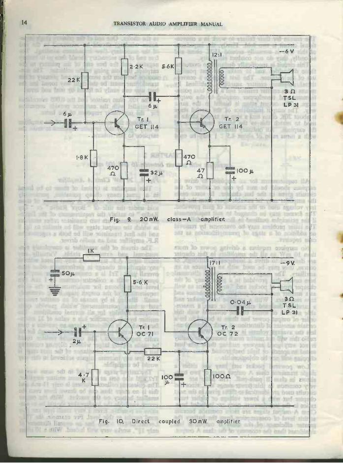
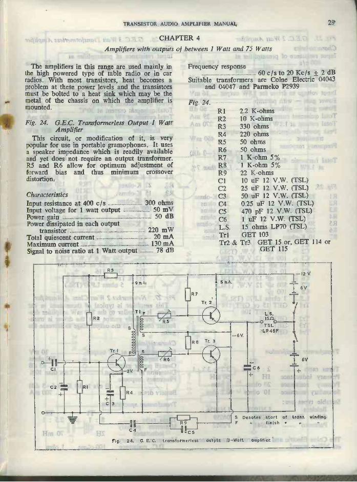
Fig. 9. 20 mW Class A AmplifierThis amplifier is typical of those to be found
in a great many cheap portables, particularlythose of Japanese origin. A great many of thesesold under the title of " Boys' Radio " or " ToyRadio " to satisfy the requirements of the Japan-ese government, are two transistor reflex receiversin which the output stage will be similar to fig. 9and the first transistor will be both a regenerativeR.F. amplifier and an audio driver.
The circuit of the amplifier is completely con-ventional and extremely stable. Virtually anysmall signal A.F. transistors may be used withoutany significant change in performance other thanoverall gain. Tr 1 is a common emitter amplifieroperating with a collector current of 1 mA thislevel being chosen for maximum gain the driverequirements of the output stage being extremelysmall. Biasing is by means of an emitter resistorand a base potentiometer which provide quiteadequate stability for all normal conditions. Theemitter bypass capacitor has a value of 32 micro -farads which is sufficiently large to provide a bassresponse which is more than good enough for allradio requirements. The collector resistor couldbe made slightly larger without clipping occurringbut since the input impedance of the next stage isvery low any increase in gain achieved in this waywould be negligible.
The output stage is biased in the same way asTr2 and also acts as a common emitter amplifier.The quiescent collector current is only 11 mA andthis is no more than can be drawn from even thesmallest battery on the market. With the outputpower available the loudspeaker should be as sen-sitive as possible. Even a very small type can givegood results at this level. For example, the TSL-Lorenz LP45F which has an overall diameter ofonly 11", works very well indeed. With a 10 ohms
14 TRANSISTOR AUDIO AMPLIFIER MANUAL
22 K
6p,
I
1.8 K
IK
eon 50y,
AMMO.AM=
470-Cl
2.2K 5.6K
6p,
Tr. I
GET 114
1 32p,
470
47n
12:1
Tr. 2GET 114
Fig. 9 20 mW. class-A amplifier.
100p,
-6 V
3nTSLLP 31
4.7K
5.6 K
22 K
17:1
aaaaaaaa
100JL
Tr. 2OC 72
loon
-9 V.
3nTSLLP 31
Fig. 10. Direct coupled 30 mW. amplifier.
TRANSISTOR AUDIO AMPLIFIER MANUAL 15
speaker the turns ratio of the output transformershould be about 6.5 : 1.
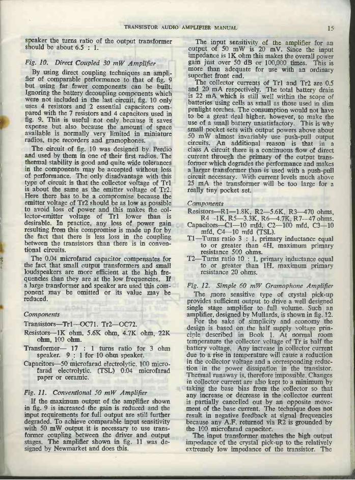
Fig. 10. Direct Coupled 30 mW AmplifierBy using direct coupling techniques an ampli-
fier of comparable performance to that of fig. 9but using far fewer components can be built.Ignoring the battery decoupling components whichwere not included in the last circuit, fig. 10 onlyuses 4 resistors and 2 essential capacitors com-pared with the 7 resistors and 4 capacitors used infig. 9. This is useful not only because it savesexpense but also because the amount of spaceavailable is normally very limited in miniatureradios, tape recorders and gramophones.
The circuit of fig. 10 was designed by Perdioand used by them in one of their first radios. Thethermal stability is good and quite wide tolerancesin the components may be accepted without lossof performance. The only disadvantage with thistype of circuit is that the collector voltage of Trlis about the same as the emitter voltage of Tr2.Here there has to be a compromise because theemitter voltage of Tr2 should be as low as possibleto avoid loss of power and this makes the col-lector -emitter voltage of Tr 1 lower than isdesirable. In practice, any loss of power gainresulting from this compromise is made up for bythe fact that there is less loss in the couplingbetween the transistors than there is in conven-tional circuits.
The 0.04 microfarad capacitor compensates forthe fact that small output transformers and smallloudspeakers are more efficient at the high fre-quencies than they are at the low frequencies. Ifa large transformer and speaker are used this com-ponent may be omitted or its value may bereduced.
Components
Transistors-Tr1-0C71. Tr2-0072.Resistors -1K ohm, 5.6K ohm, 4.7K ohm, 22K
ohm, 100 ohm.Transformer- 17 : 1 turns ratio for 3 ohm
speaker. 9 : 1 for 10 ohm speaker.Capacitors-SO microfarad electrolytic. 100 micro -
farad electrolytic. (TSL) 0.04 microfaradpaper or ceramic.
Fig. 11. Conventional 50 mW AmplifierIf the maximum output of the amplifier shown
in fig. 9 is increased the gain is reduced and theinput requirements for full output are still furtherdegraded. To achieve comparable input sensitivitywith 50 mW output it is necessary to use trans-former coupling between the driver and outputstages. The amplifier shown in fig. 11 was de-signed by Newmarket and does this.
The input sensitivity of the amplifier for anoutput of 50 mW is 20 mV. Since the inputimpedance is 1K ohm this makes the overall powergain just over 50 dB or 100,000 times. This ismore than adequate for use with an ordinarysuperhet front end.
The collector currents of Tr 1 and Tr2 are 0.5and 20 mA respectively. The total battery drainis 22 mA which is still well within the scope ofbatteries using cells as small as those used in slimpenlight torches. The consumption would not haveto be a great deal higher, however, to make theuse of a small battery unsatisfactory. This is whysmall pocket sets with output powers above about50 mW almost invariably use push-pull outputcircuits. An additional reason is that in aclass A circuit there is a continuous flow of directcurrent through the primary of the output trans-former which degrades the performance and makesa larger transformer than is used with a push-pullcircuit necessary. With current levels much above25 mA the transformer will be too large for areally tiny pocket set.
ComponentsResistors-R1-1.8K, R2 -5.6K, R3-470 ohms,
R4 -1K, R5 -3.3K, R6 -4.7K, R7-47 ohms.Capacitors-C1-10 mfd, C2-100 mid, C3-10
mfd, C4-10 mfd (TSL).T1-Turns ratio 3 : 1, primary inductance equal
to or greater than 4H, maximum primaryresistance 500 ohms.
T2-Turns ratio 10 : 1, primary inductance equalto or greater than 1H, maximum primaryresistance 20 ohms.
Fig. 12. Simple 60 mW Gramophone AmplifierThe more sensitive type of crystal pick-up
provides sufficient output to drive a well designedsingle stage amplifier to full volume. Such anamplifier, designed by Mullards, is shown in fig. 12.
For the sake of simplicity and economy thedesign is based on the half supply voltage prin-ciple described in Book 1. At normal roomtemperature the collector voltage of Tr is half thebattery voltage. Any increase in collector currentdue to a rise in temperature will cause a reductionin the collector voltage and a corresponding reduc-tion in the power dissipation in the transistor.Thermal runaway is, therefore impossible. Changesin collector current are also kept to a minimum bytaking the base bias from the collector so thatany increase or decrease in the collector currentis partially cancelled out by an opposite move-ment of the base current. The technique does notresult in negative feedback at signal frequenciesbecause any A.F. returned via R2 is grounded bythe 100 microfarad capacitor.
The input transformer matches the high outputimpedance of the crystal pick-up to the relativelyextremely low impedance of the transistor. The
16 TRANSISTOR AUDIO AMPLIFIER MANUAL
imL-C 2
21001ERI18K
CI
I1011.
RI2MLog.
R2470,f).
1#-I IC410p
-R647011
T2
10:1
Tr. 2V10/30A
R74711
-6V.
3nUsk
TSL LP3I
Fig. It. Conventional 50 mW. amplifier. (Newmarket)
45:Ia
111--aaaa
R2100 K
aa
lOO p.
Tr.OC 72
14011
-9V
Fig. 12. Simple 60 mW. gramophone amplifier by Mallard.
TRANSISTOR AUDIO AMPLIFIER MANUAL 17
S
turns ratio is 45 : 1 and the primary inductanceshould be at least 250H and preferably about twicethis.
The maximum efficiency of the amplifier is only25% because half the power is dissipated in theloudspeaker's D.C. resistance. As the temperaturerises the maximum efficiency and power outputboth drop but with a really sensitive loudspeakerthe sound level should remain quite sufficient. Thecollector voltage should be adjusted, at 25°C, to4.5 volts by altering R2.
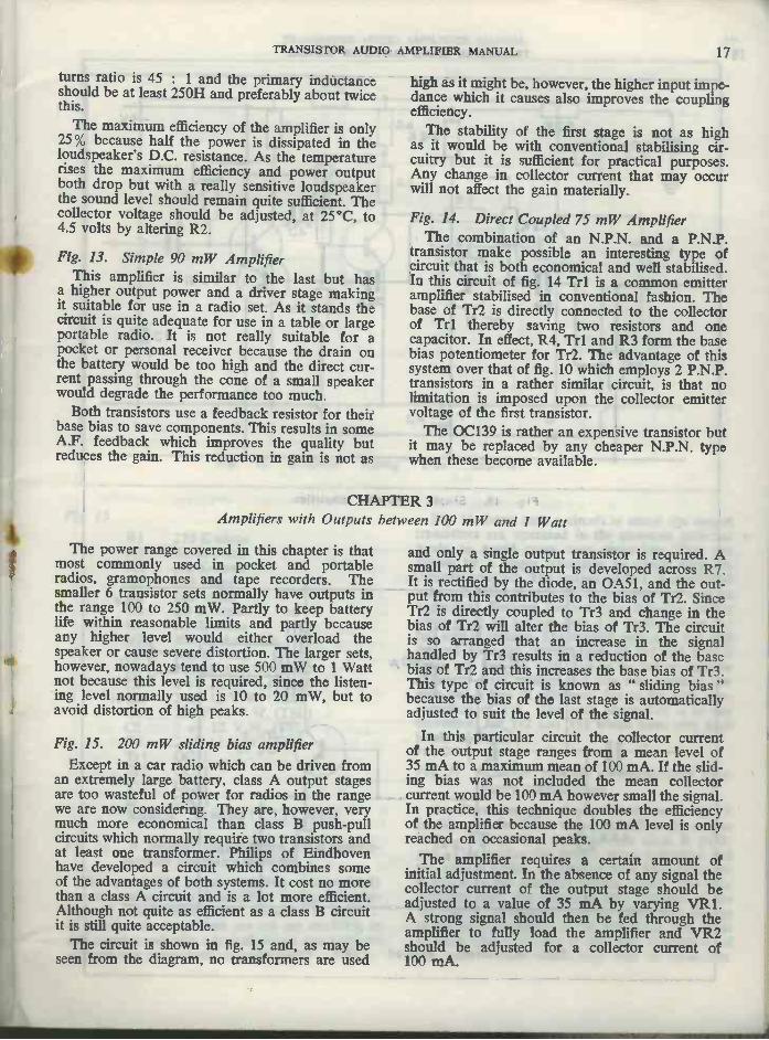
Fig. 13. Simple 90 mW AmplifierThis amplifier is similar to the last but has
a higher output power and a driver stage makingit suitable for use in a radio set. As it stands thecircuit is quite adequate for use in a table or largeportable radio. It is not really suitable for apocket or personal receiver because the drain onthe battery would be too high and the direct cur-rent passing through the cone of a small speakerwould degrade the performance too much.
Both transistors use a feedback resistor for theirbase bias to save components. This results in someA.F. feedback which improves the quality butreduces the gain. This reduction in gain is not as
high as it might be, however, the higher input impe-dance which it causes also improves the couplingefficiency.
The stability of the first stage is not as highas it would be with conventional stabilising cir-cuitry but it is sufficient for practical purposes.Any change in collector current that may occurwill not affect the gain materially.
Fig. 14. Direct Coupled 75 mW AmplifierThe combination of an N.P.N. and a P.N.P.
transistor make possible an interesting type ofcircuit that is both economical and well stabilised.In this circuit of fig. 14 Tr 1 is a common emitteramplifier stabilised in conventional fashion. Thebase of Tr2 is directly connected to the collectorof Tr 1 thereby saving two resistors and onecapacitor. In effect, R4, Tr 1 and R3 form the basebias potentiometer for Tr2. The advantage of thissystem over that of fig. 10 which employs 2 P.N.P.transistors in a rather similar circuit, is that nolimitation is imposed upon the collector emittervoltage of the first transistor.
The 0C139 is rather an expensive transistor butit may be replaced by any cheaper N.P.N. typewhen these become available.
CHAPTER 3Amplifiers with Outputs between 100 mW and 1 Watt
The power range covered in this chapter is thatmost commonly used in pocket and portableradios, gramophones and tape recorders. Thesmaller 6 transistor sets normally have outputs inthe range 100 to 250 mW. Partly to keep batterylife within reasonable limits and partly becauseany higher level would either overload thespeaker or cause severe distortion. The larger sets,however, nowadays tend to use 500 mW to 1 Wattnot because this level is required, since the listen-ing level normally used is 10 to 20 mW, but toavoid distortion of high peaks.
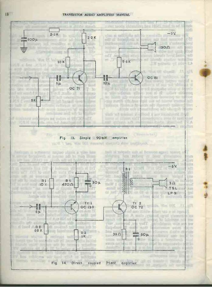
Fig. 15. 200 mW sliding bias amplifierExcept in a car radio which can be driven from
an extremely large battery, class A output stagesare too wasteful of power for radios in the rangewe are now considering. They are, however, verymuch more economical than class B push-pullcircuits which normally require two transistors andat least one transformer. Philips of Eindhovenhave developed a circuit which combines someof the advantages of both systems. It cost no morethan a class A circuit and is a lot more efficient.Although not quite as efficient as a class B circuitit is still quite acceptable.
The circuit is shown in fig. 15 and, as may beseen from the diagram, no transformers are used
and only a single output transistor is required. Asmall part of the output is developed across R7.It is rectified by the diode, an 0A51, and the out-put from this contributes to the bias of Tr2. SinceTr2 is directly coupled to Tr3 and change in thebias of Tr2 will alter the bias of Tr3. The circuitis so arranged that an increase in the signalhandled by Tr3 results in a reduction of the basebias of Tr2 and this increases the base bias of Tr3.This type of circuit is known as " sliding bias "because the bias of the last stage is automaticallyadjusted to suit the level of the signal.
In this particular circuit the collector currentof the output stage ranges from a mean level of35 mA to a maximum mean of 100 mA. If the slid-ing bias was not included the mean collectorcurrent would be 100 mA however small the signal.In practice, this technique doubles the efficiencyof the amplifier because the 100 mA level is onlyreached on occasional peaks.
The amplifier requires a certain amount ofinitial adjustment. In the absence of any signal thecollector current of the output stage should beadjusted to a value of 35 mA by varying VR1.A strong signal should then be fed through theamplifier to fully load the amplifier and VR2should be adjusted for a collector current of100 mA.
18 TRANSISTOR AUDIO AMPLIFIER MANUAL
100p,
5K
22K
33 K
I
6p,
OC 71
2.2K
OC 81
-9V
130n
Fig I3, Simple 90mW. amplifier.
R I10.K
R268K
R44701.11
8:1
Tr. I
OC 139
R3Ix 39n
Fig. 14. Direct coupled 75m1f1. amplifier.
-6V.
3aT S L
LP 31
TRANSISTOR AUDIO AMPLIFIER MANUAL 19
4
R3
RI
C2> I I+
Fig. 15.
R2
1VRI
Fig. IS. 200mW.
R4
RS
sliding
Tr. 3
bias amplifier.
D
+14
R7
airOMMIS.
R1R2R3R4R5R6R7VR1VR2ClC2C3C4C5
270 K -ohms2.2 K -ohms2.2 K -ohms560 ohms560 ohms3.9 K -ohms1.5 K -ohms200 K -ohms Lin.150 K -ohms100 uF 6 V.W. (TSL)2 uF 12 V.W. (TSL)2 uF 12 V.W. (TSL)25 uF 12 V.W. (TSL)2 uF 12 V.W. (TSL)
C6 2 uF 12 V.W. (TSL)Trl 0071Tr2 0071Tr3 0081D 0A51Speaker 50 ohms (TSL) CMS50
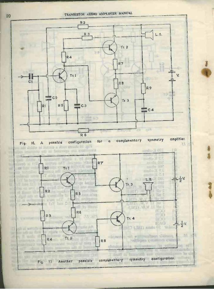
Fig. 16. A possible configuration for a comple-mentary symmetry amplifier
The possibility of constructing a completelytransformerless class B amplifier using the prin-ciple of complementary was discussed in Book 1.In practice the transistors are not yet available inthis country and only a typical circuit can be givenwithout any component values
Fig. 16 shows such a circuit in which the outputtransistors are operated in the common collectormode to avoid cross over distortion. They aredriven by a single transistor to which they aredirectly coursed. The output of Trl is developedacross R3 (R4 is very small in value and may beneglected). Because the common collector outputstage gi% ts no voltage gain Trl must develop thefull output voltage. The current output of Tr I willdepend upon the current gains of Tr2 and Tr3. Ifthese are low R3 will have to be low to achievesufficient drive voltage and this will result in lowgain and a loss of efficiency due to the high con-sumption of Trl. The only alternative is to usetransistors for Tr2 and Tr3 which have very highlevels of Beta.
Fig. 17. Another possible complementary sym-metry configuration
An alternative type of circuit is shown in fig. 17.In this case the driver stage, as well as the outputstage, employs two transistors in class B push-pull. This makes the circuit more expensive butthe gain is higher because all four transistors areoperated in the common emitter mode. The onlydifficulty with this system is that, because of theD.C. coupling between the two stages, any changein the bias conditions of the first stage will causea much larger change in the bias conditions ofthe output stage which may lead to instability
20TRANSISTOR AUDIO AMPLIFIER MANUAL
---11CI
RI
R2
C 2ono
R5
R3
Tr 2
R7
R8
Tr. 3
R9
=C4
L. S.
R6
Fig. 16. A possible configuration for a complementary symmetry amplifier.
2V.
2
RI
R2
R3
R4
Tr. I
Tr. 2
R5
R6
R7
R8
Tr.. 3
L.S
Tr. 4
Fig. 17 Another possible complementary symmetry configuration.
TRANSISTOR AUDIO AMPLIFIER MANUAL 21
cIt
RI
R3
Tr. I
C2
P2
R4
T
00
R5
R6
Tr. 2
R9
Tc 3
R7
R8
T2
Fig. 18. G. E. C. 250mW. amplifier with symmetrical output.
-6V.
L.S.
The only cure for this is to include resistors R5and R6 in the emitters of the first two transistors.These can not be bypassed by electrolytic capaci-tors in the normal way because the rectifyingaction of the base -emitter junction would chargethem up to the point where they would alter thebias conditions themselves. R5 and R6. therefore,cause a loss of gain.
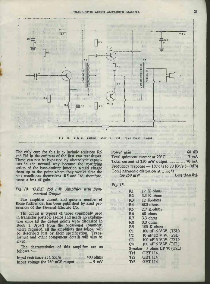
Fig. 18. G.E.C. 250 mW Amplifier with Sym-metrical Output
This amplifier circuit. and quite a number ofthose further on, has been published by kind per-mission of the General Electric Co.
The circuit is typical of those commonly usedin transistor portable radios and needs no explana-tion since all the design points were discussed inBook 1. Apart from the occasional comment,where required, all the amplifiers that follow willbe described just by their specification. Trans-former and other component details will also begiven.
The characteristics of this amplifier are asfollows :-Input resistance at 1 Kc/s 400 ohmsInput voltage for 250 mW output 9 mV
Power gain 60 dBTotal quiescent current at 20T 7 mATotal current at 250 mW output 70 mAFrequency response - 150 c/s to 20 Kc/s (-3dB)Total harmonic distortion at 1 Kc/s
for. 250 mW Less than 8%
Fig. 18.
RI 12 K -ohmsR2 3.3 K -ohmsR3 12 K -ohmsR4 680 ohmsR5 2.7 K -ohmsR6 68 ohmsR7 3.3 ohmsR8 3.3 ohmsR9 100 K -ohmsCl 100 uF 6 V.W. (TSL)C2 10 uF 12 V.W. (TSL)C3 100 uF 3 V.W. (TSL)C4 100 uF 6 V.W. (TSL)Speaker 3 ohms LP 70 (TSL)Trl GET 114Tr2 GET 114Tr3 GET 114
22 TRANSISTOR AUDIO AMPLIFIER MANUAL
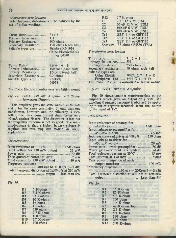
Transformer specificationsTotal harmonic distortionuse of bifilar windings.
Turns RatioPrimary InductancePrimary ResistanceSecondary ResistanceSuitable types are:
Turns RatioPrimary InductancePrimary ResistanceSecondary ResistanceSuitable types are :
will be reduced by the
Ti3 :1 + I4H500 ohms150 ohms (each half)Belclere KN1936Colne Electric 04073
or 04070
T24.6 + 4.6 : 1
150 mH (each half)1.5 ohm (each half)0.2 ohmsKNI93704074
The Colne Electric transformers are bifilar wound
Fig. 19. G.E.C. 250 mW Amplifier with Trans-formerless Output.
This amplifier gives the same output as the lastand it has the same sensitivity. It only uses onetransformer, however, and the efficiency is 75%better, the maximum current drain being only40 mA against 70 mA. The distortion is less butthe frequency response is not so good. The maindisadvantage is that a higher battery voltage isrequired but this may not matter in manyapplications.
Characteristics
Input resistance at 1 Kc/s 2.5K ohmsInput voltage for 230 mW output 25 mVPower gain 70 dBTotal quiescent current at 20°C 7 mATotal current for 230 mW output 40 mAFrequency response
200 c/s to 11 Kc/s (-3 dB)Total harmonic distortion at 1.000 c/s at 230 mW
output - less than 6%
R12ClC2C3C4TrlTr2Tr3Speakers
2.7 K -ohms2 uF 12 V.W. (TSL)50 uF 12 V.W. (TSL)100 uF 6 V.W. (TSL)100 uF 6 V.W. (TSL)GET 114 or GET 15GET 114 or GET 15GET 114 or GET 1538 ohms CMS50 (TSL)
Transformer specification
Turns ratioPrimary InductancePrimary resistanceSecondary resistanceSuitable types are-
Colne Electric 04070 (3.2 : 1 + 1)Fortiphone Ltd. 4442 (7 : 1 + 1)
The Colne Electric Transformer is bifilar wound.
7 1 + 15H250 ohms40 ohms each half
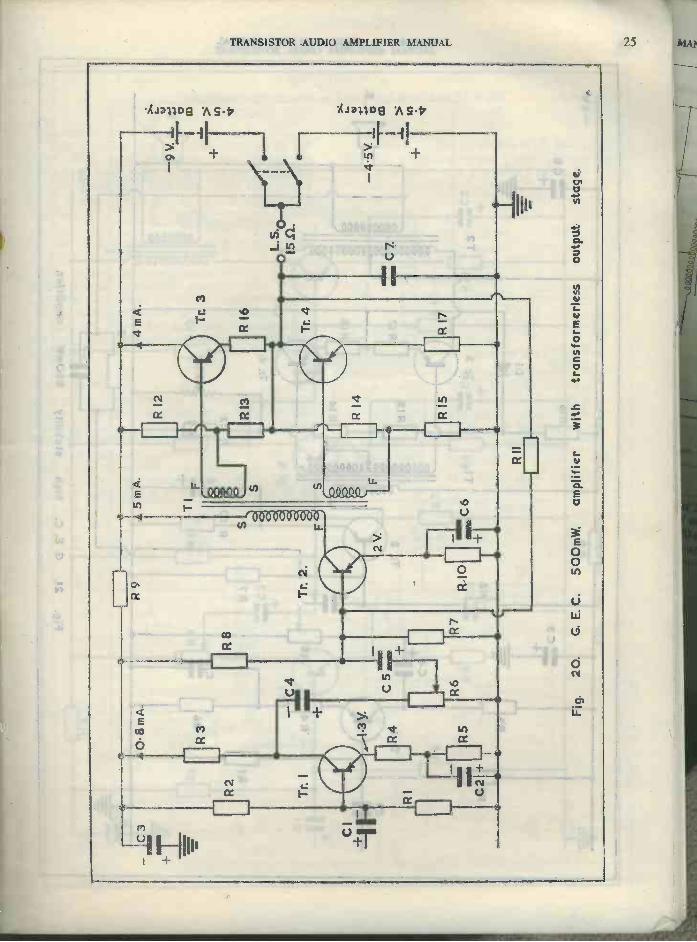
cig. 20. G.E.C. 500 mW Amplifier.
Fig. 20 shows another transformerless outputamplifier which gives an output of watt. Anexcellent frequency response is obtained by apply-ing 6 dB of negative feedback from the outputto the input of Tr2.
Characteristics
Input resistance of preamplifierat 400 c/s 4.5K ohms
Input voltage to preamplifier for450 mW output 7.5 mV
Input resistance of driver at 400 c/t 250 ohmsInput voltage to driver for
450 mM output 20 mVPower gain - with preamplifier 76 dBPower gain - without preamplifier 54 dBTotal quiescent current at 20°C. 15 mATotal current at 450 mW 85mAPeak power dissipation of each
output transistor 100 mWFrequency response
90 c/s - 20Kc/s ( - 3 dB)Total harmonic distortion at 400 c/s at 450 mW
Fig. 19.
output
Fig. 20.
Less than 5%
RI 5 K -ohms RI 15 K -ohmsR2 3.3 K -ohms R2 82 K -ohmsR3 33 K -ohms R3 5.6 K -ohmsR4 10 K -ohms R4 100 ohmsR5 15 ohms R5 1.5 K -ohms
47 K -ohms log.R6 1 K -ohm R6R7 680 ohms R7 2.2 K -ohmsR8 2.7 K -ohms R8 6.8 K -ohmsR9 100 ohms R9 390 ohmsRIO 2.7 K -ohms R10 390 ohmsR11 100 ohms R11 100 K -ohms
TRANSISTOR AUDIO AMPLIFIER MANUAL 23
R12 1 K -ohmR13 39 ohmsR14 1 K -ohmR15 39 ohmsR16 2.2 ohmsR17 2.2 ohmsCI 10 uF 12 V.W. (TSL)C2 100 uF 3 V.W. (TSL)C3 100 uF 12 V.W. (TSL)C4 10 uF 12 V.W. (TSL)C5 10 uF 12 V.W. (TSL)C6 100 uF 6 V.W. (TSL)C7 0.5 uFTrl GET 114 or GET 15Tr2 GET 114 or GET 15Tr3 GET 114 or GET 15Tr4 GET 114Speaker 15 ohms LP45F (TSL)
Transformer Specification
Turns ratio 3 : 1 -I- 1
Primary Inductance 3HPrimary resistance 100 ohmsSecondary resistance 20 ohms each sectionSuitable types are :
Colne Electric 04043Parmeko P2937
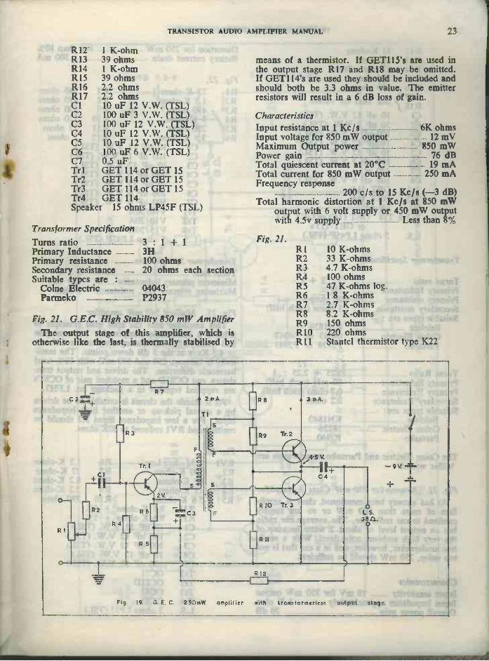
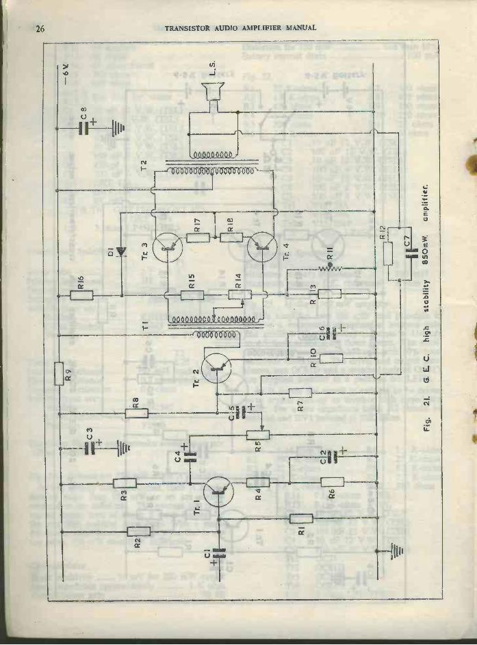
Fig. 21. G.E.C. High Stability 850 mW AmplifierThe output stage of this amplifier, which is
otherwise like the last, is thermally stabilised by
means of a thermistor. If GET115's are used inthe output stage R17 and R18 may be omitted.If GET114's are used they should be included andshould both be 3.3 ohms in value. The emitterresistors will result in a 6 dB loss of gain.
CharacteristicsInput resistance at 1 Kc/s 6K ohmsInput voltage for 850 mW output 12 mVMaximum Output power 850 mWPower gain 76 dBTotal quiescent current at 20°C 19 mATotal current for 850 mW output 250 mAFrequency response
200 c/s to 15 Kc/s (-3 dB)Total harmonic distortion at 1 Kc/s at 850 mW
output with 6 volt supply or 450 mW outputwith 4.5v supply Less than 8%
Fig. 21.R 1 10 K -ohmsR2 33 K -ohmsR3 4.7 K -ohmsR4 100 ohmsR5 47 K -ohms log.R6 1.8 K -ohmsR7 2.7 K -ohmsR8 8.2 K -ohmsR9 150 ohmsRIO 220 ohmsR 11 Stantel thermistor type K22
2
RI
0
R3
Tr. I
R4
R6
95
7
2V.
2 mA.
TI
F0
S
C3
OR 8
8
0
F
99 Tr.2
R 12
3 m A.
4'5 V.
04
OL.S.38/1.0
Fig. 19, G. E. C. 2.50mW. amplifier with trair.tformtriess output Stage.
24 TRANSISTOR AUDIO AMPLIFIER MANUAL
R12 47 K -ohmsR13 68 ohmsR14 47 ohms PresetR15 180 ohmsR16 680 ohmsR17 } See Text for valuesR18Cl 10 uF 12 V.W. (TSL)C2 50 uF 3 V.W. (TSL)C3 100 uF 6 V.W. (TSL)C4 10 uF 12 V.W. (TSL)C5 10 uF 12 V.W. (TSL)C6 100 uF 3 V.W. (TSL)C7 470 pfC8 100 uF 6 V.W. (TSL)Trl GET 114Tr2 GET 114D1 SX 640Tr3 & Tr4 GET 114's or GET 15's
or GET 115'sL.S. 3 ohms LP45F (TSL)
Transformer Specification
Turns ratioPrimary InductancePrimary resistanceSecondary resistanceSuitable types are :-
BelclereColne ElectricParmeko
Turns RatioPrimary InductancePrimary ResistanceSecondary ResistanceSuitable types are -
Belclere KN1840Colne Electric 18226Parmeko P2940
T12 : 1 + 12H20 ohms5 ohms (each half)
KN183904043 or 04047P2939 or P2941
T22.25 + 2.25 : 1
50 mH (each half)0.7 ohms (each half)0.2 ohms
The Colne Electric and Parmeko transformers arebifilar wound.
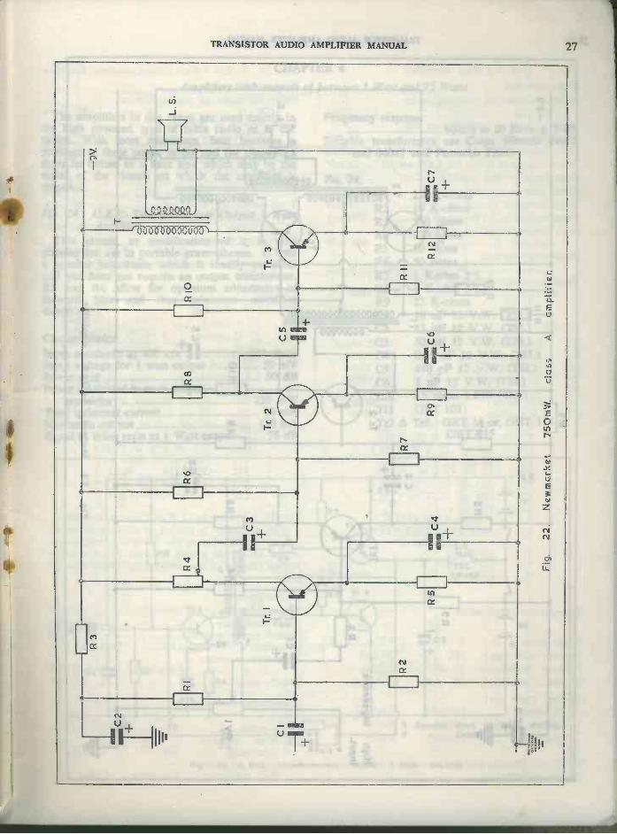
Fig. 22. Newmarket 750 mW Class A AmplifierAs has already been mentioned, class A ampli-
fiers of more than 100 mW or so are mainlyconfined to car radio use. The average car radiohas an output level of about 2 watts because ofthe very high ambient noise level. With a sensi-tive loudspeaker, however, and in a car that is nottoo noisy, 750 mW should be sufficient.
CharacteristicsInput sensitivity 10 mV for 750 mW outputInput impedance approximately 1 IC ohmOverall power gain 70 dB
Distortion for 750 mWBattery current drain
Fig. 22.
less than 10%300 mA
RI 22 K -ohms R7 560 ohmsR2 1.8 K -ohms R8 470 ohmsR3 470 ohms R9 100 ohmsR4 3 K -ohms RIO 220 ohmsR5 220 ohms R11 22 ohmsR6 3.9 K -ohms R12 5 ohms
Cl 10 uF 12 V.W. (TSL)C2 100 uF 12 V.W. (TSL)C3 10 uF 12 V.W. (TSL)C4 100 uF 6 V.W. (TSL)C5 10 uF 12 V.W. (TSL)C6 100 uF 6 V.W. (TSL)C7 500 uF 6 V.W. (TSL)Trl V10/50ATr2 V10/ 30ATr3 V15/201PL.S. 3 ohms LP45F (TSL)
Transformer SpecificationTurns ratioMinimum primary inductanceMaximum primary D.C. resistance
3 : 1
130 mH1 ohm
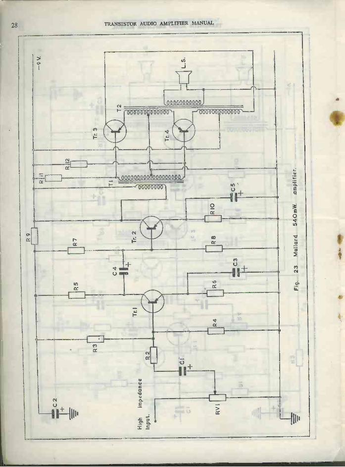
Fig. 23. Mullard 540 mW amplifierThis amplifier uses the split load principle to
achieve a reasonable compromise between gainand quality. The frequency response is 110 c/sto 4.3 Kc/s at the 3 dB down points. The sensi-tivity is between 250 and 350 mV with 10% totalharmonic distortion. The driver and output tran-sistors, one OC81D and a matched pair of 0081'sare supplied together in a package no. LFH3.
As it stands the circuit is suitable to be drivenby a crystal pick-up or another high impedanceinput. For a low impedance input R2 should beomitted and RV1 reduced to 50K ohms.
Fig. 23.RV1 1 M -ohm Log. R6 1.2 K -ohmsR2 390 K -ohms R7 27 K -ohmsR3 82 K -ohms R8 8.2 K -ohmsR4 15 K -ohms R9 2.2 K -ohmsR5 5.6 K -ohms R10 390 ohms
R11 9.1 K -ohms ± 5%R12 9.1 K -ohms ± 5%Cl 10 uF 12 V.W. (TSL)
100 uF 12 V.W. (TSL)100 uF 12 V.W. (TSL)10 uF 12 V.W. (TSL)100 uF 12 V.W. (TSL)0071OC81D008100813 ohms LP31 (TSL)
C2C3C4C5TrlTr2Tr3Tr4L.S.
-13
R2
tC-8
mA
.,
R3
R4
R5
C5_
4 R6
R8 R
7
R9
Tr.
2.
FOJ
Fig
.20
.G
. E. C
.50
0mW
.am
plifi
erw
ithtr
ansf
orm
erle
ssou
tput
stag
e.
R2
CI
Tr.
I R4
RI
C4 I+ R
5
R8
RI6
DI
R9
TI
Tr
2
Tr.
3
R 1
2
C TT
2
Fig
.21
.G
. E. C
.hi
ghst
abili
ty85
0rA
W.
ampl
if le
r.
-6V
TRANSISTOR AUDIO AMPLIFIER MANUAL 27
(Tv. 0 0 0 0 U -TO -CM
0
U
U
0LC1
N
R9
'C2
Hig
him
peda
nce
Inpu
t.
RV
I
R3
Tr.
I
R2
R4
R5
C4
s-I 4
11-7
-
R6
C3
R7 Tr.
2
T a ad a a
RIO
MIM
IC 5
low
R
a a
11
12
Tr.
3
Tr.
4
T2
a 0 a #10 a
-9 V
.
L.S
.
Fig
.23
.M
ulla
rd54
0mW
.am
plifi
er.
TRANSISTOR AUDIO AMPLIFIER MANUAL 29
I
CHAPTER 4
Amplifiers with outputs of between 1 Watt and 75 Watts
The amplifiers in this range are used mainly inthe high powered type of table radio or in carradios. With most transistors, heat becomes aproblem at these power levels and the transistorsmust be bolted to a heat sink which may be themetal of the chassis on which the amplifier ismounted.
Fig. 24. G.E.C. Transformerless Output 1 WattAmplifier
This circuit, or modification of it, is verypopular for use in portable gramophones. It usesa speaker impedance which is readily availableand yet does not require an output transformer.R5 and R6 allow for optimum adjustment offorward bias and thus minimum crossoverdistortion.
CharacteristicsInput resistance at 400 c/s 300 ohmsInput voltage for 1 watt output 50 mVPower gain 50 dBPower dissipated in each output
transistor 220 mWTotal quiescent current 20 mAMaximum current 130 mASignal to noise ratio at 1 Watt output 78 dB
Frequency response60 c/s to 20 Kc/s ± 2 dB
Suitable transformers are Comm Electric 04043and 04047 and Parmeko P2939
Fig. 24.R1R2R3R4R5R6R7R8R9ClC2C3C4C5C6L.S.
2.2 K -ohms10 K -ohms330 ohms220 ohms50 ohms50 ohms1 K -ohm 5%1 K -ohm 5%22 K -ohms10 uF 12 V.W. (TSL)25 uF 12 V.W. (TSL)50 uF 12 V.W. (TSL)0.25 uF 12 V.W. (TSL)470 pF 12 V.W. (TSL)1 uF 12 V.W. (TSL)15 ohms LP70 (TSL)
Trl GET 103Tr2 & Tr3 GET 15 or, GET 114 or
GET 115
R2
R3
Tr. I
CI
C2
O t_
RI
-I-C 3
-2V
R4
9 m A.
R7
Tr. 2
R5
A 5 mA.
0O F
R 8 Tr. 3
R6
-6V.
= C 6
L.S.Isn.TSL
LP 45F
12 V.
I 6V
C4
Fig. 24. G. E. C.
{-R9
--11FET
6V
S Denotes start of trans. winding.F finish
transformerless output 1-Watt. amplifier
30 TRANSISTOR AUDIO AMPLIFIER MANUAL
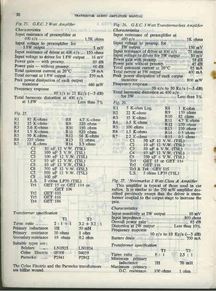
Fig. 25. G.E.C. 2 Watt AmplifierCharacteristicsInput resistance of preamplifier at
400 c/s 1.5K ohmsInput voltage to preamplifier for
1.8W output 5 mVInput resistance of driver at 400 c/s 150 ohmsInput voltage to driver for 1.8W output 16 mVPower gain - with preamp. 80 dBPower gain - without preamp. 60 dBTotal quiescent current at 20°C 29 mATotal current at 1.8W output 270 mAPeak power dissipation of each output
transistor 460 mWFrequency response
60 c/s to 22 Kc/s (-3 dB)Total harmonic distortion at 400 c/s
at 1.8W Less than 7%
Fig. 25.R1 82 K -ohmsR2 15 K -ohmsR3 5.6 K -ohmsR4 1.5 K -ohmsR5 50 K -ohmsR6 220 ohmsR7 10 K -ohms
ClC2C3C4C5C6C7C8L.S.Trl
Tr2Tr3Tr4
R8 4.7 K -ohmsR9 220 ohmsR10 150 ohmsR11 820 ohmsR12 56 K -ohmsR13 12 ohmsR14 3.3 ohms
10 uF 12 V.W. (TSL)100 uF 3 V.W. (TSL)100 uF 12 V.W. (TSL)10 uF 12 V.W. (TSL)10 uF 12 V.W. (TSL)500 uF 12 V.W. (TSL)500 uF 12 V.W. (TSL)100 pF3 ohms LP70 (TSL)GET 15 or GET 114 or
GET 106GET 103GET 116GET 116
Transformer specification
T1Turns ratio 2 : 1 + 1Primary inductance 1HPrimary resistance 20 ohmsSecondary resistance 10 ohmsSuitable types are :
Belclere LN1923Colne Electric 05008Parmeko P2941
T23.2 ± 3.2 : 1
50 mH1 ohm0.2 ohm
LN192404059P2942
The Colne Electric and the Parmeko transformersare bifilar wound.
Fig. 26. G.E.C. 3 Watt Transformerless AmplifierCharacteristicsInput resistance of preamplifier at
400 c/s 5K ohmsInput voltage to preamp. for
3W output 150 mVInput resistance of driver at 400 c/s 75 ohmsInput voltage to driver for 3W output 80 mVPower gain with preamp. 58 dBPower gain without preamp. 45 dBTotal quiescent current at 20°C 65 mATotal current at 3W output 400 mAPeak power dissipation of each output
transistor 800 mWFrequency response
20 c/s to 30 Kc/s (-3 dB)Total harmonic distortion at 400 c/s
for 3W
Fig. 26.
Less than 5%
R1 5 K -ohm Log. R8 1 K -ohmR2 22 K -ohms R9 150 ohmsR3R4
15 K -ohms1.5 K -ohms
RIOR11R12
82 ohms4.7 K -ohms270 ohmsR5 100 ohms R13 270 ohms
R6 1.5 K -ohms R14 0.5 ohmsR7 2.2 K -ohms R15 0.5 ohms
Cl 50 uF 12 V.W. (TSL)C2 10 uF 12 V.W. (TSL)C3 50 uF 6 V.W. (TSL)C4 10 uF 12 V.W. (TSL)C5 250 uF 6 V.W. (TSL)Trl GET 15 or GET 114Tr2 GET 116Tr3 & Tr4 GET 115L.S. 5 ohms LP70 (TSL)
Fig. 27. Newmarket 2 Watt Class A AmplifierThis amplifier is typical of those used in car
radios. It is similar to the 750 mW amplifier des-cribed previously except that the driver is trans-former coupled to the output stage to increase thegain.
CharacteristicsInput sensitivity at 2W output 10 mVInput impedance 800 ohmsOverall power gain 65 dBDistortion at 2W output Less than 10%Frequency response
50 c/s to 10 Kc/s (-3 dB)Battery drain 700 mA
Transformer specification
Turns ratioMinimum primary
inductanceMaximum primary
D.C. resistance
T1 T28 : 1 2.5 : 1
2H 70 mH
100 ohms 1 ohm
R 1
0
[ R II
Tr.
310
In A
.
T
01
C7
LT=
R13
R12
CS
6 IN
A.
Fig
.25
.G
. E. C
.tw
o-w
att
ampl
ifier
:
T2
R 1
4
RI
Tr.
I
+c
R3
C4
R9 T
r. 2
4-4.
5 V
.
R5
C3
RS
R 1
0
c. a a a a F
4-3
V.
35 m
A.
TI F
C5
J-R
I2
R 1
3
S
6 V
.
R II
3 m
A.
Tr.
3 R14
Tr.
4
R 1
5
Fig
.26
.G
. E. C
.th
ree-
wat
ttr
ansf
orm
erle
ssou
tput
ampl
ifier
.
LS. n..
-6 V
-6V
t
Fig. 27.
TRANSISTOR AUDIO AMPLIFIER MANUAL
Fig. 28.
33
RI 50 K -ohms R7 5 K -ohms R1 47 K -ohms R7 150 ohmsR2 5.6 K -ohms R8 560 ohms R2 6.8 K -ohms R8 8 ohmsR3R4
470 ohms3.3 K -ohms R9 6 ohms R3
R43.3 K -ohms1 K -ohm
R9R10
68 ohms1 ohm
R5 470 ohms R10 1 ohm R5 2.2 K -ohms R11 470 ohmsR6 3.3 K -ohms R11 50 ohms R6 1.2 K -ohms R12 10 K -ohms
Cl 10 uF 12 V.W. (TSL)C2 100 uF 12 V.W. (TSL)C3 25 uF 12 V.W. (TSL)C4 10 uF 12 V.W. (TSL)C5 100 uF 12 V.W. (TSL)C6 1000 uF 12 V.W. (TSL)L.S. 3 ohms (TSL HiQ Flexette)Trl V10/30ATr2 V15/201PTr3 V30 /20P
ClC2C3C4C5C6
Tr lTr2Tr3
10 uF 12 V.W. (TSL)10 uF 12 V.W. (TSL)10 uF 12 V.W. (TSL)100 uF 12 V.W. (TSL)25 uF 12 V.W. (TSL)100 uF 12 V.W. (TSL)3 ohms LP215 (TSL)V10/30AV10/30AV15/30P
Fig. 28. Newmarket 3 Watt Class A AmplifierCharacteristics Transformer specificationInput sensitivity for 3 watts output 20 mV T1 T2Input impedance 800 ohms Turns ratio 5 : 1 1 : 1
Power gainDistortion for 3 watts outputFrequency response
65 dBLess than 10% Maximum primary
inductance 0.8H 24 mH
50 c/s to 15 Kc/s (-3 dB) Maximum primaryBattery drain 1,150 mA D.C. resistance 20 ohms 0.5 ohms
C2
CSI
R3
RI
Tr. I
R2
RS
R4
C4
C3
R6
Tr. 2
R7
C5
TI
2
Clq
R8
R II
Tr. 3
R9
T2
P
R 10
-12 V.
L.S.
Fig. 27. Newmarket two-watt class A amplifier.
34 TRANSISTOR AUDIO AMPLIFIER MANUAL
RI
CI>1i
R2i1
I
R eye4
R6
17
Tr. 2
RI2
TI R9
a c>
0
624.4i
C 5R8
Tr. 3
T2
R 10
-9 V
L.S.
Fig. 28. Newmarket three-watt class A amplifier.
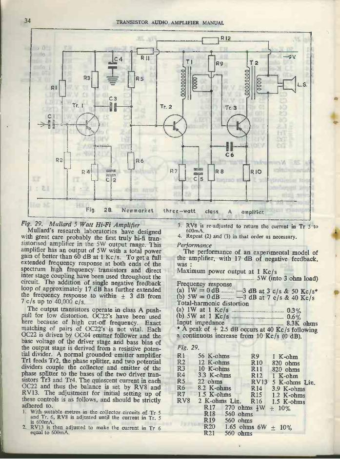
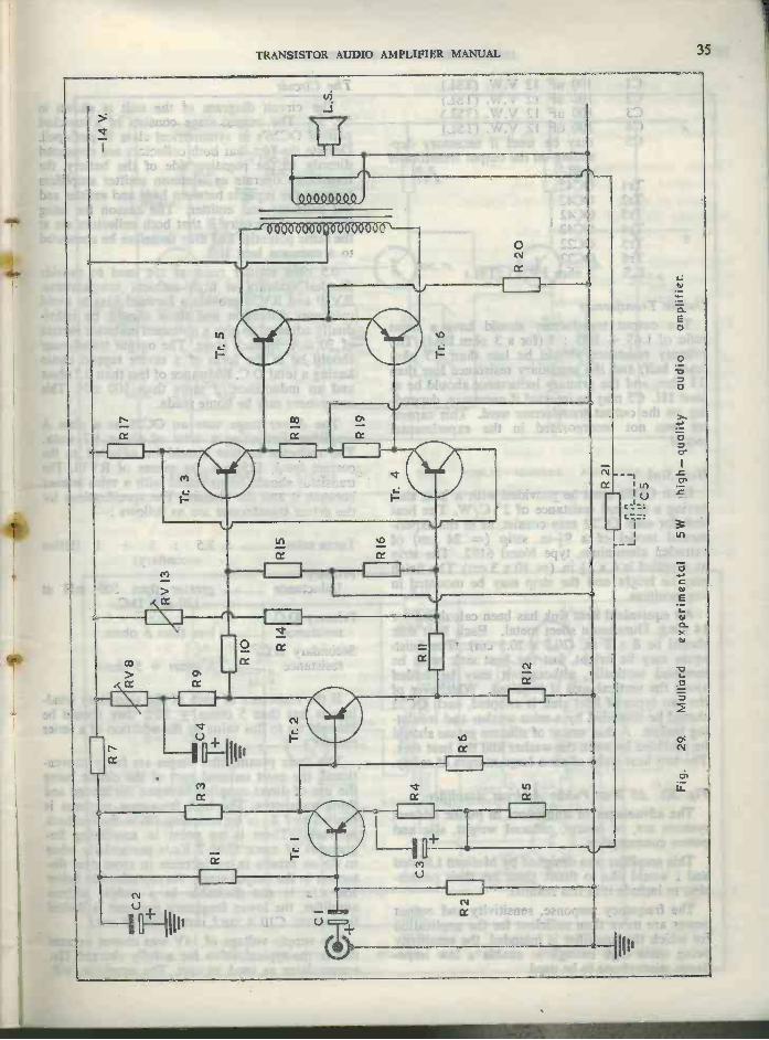
Fig. 29. Mullard 5 Watt Hi-Fi AmplifierMullard's research laboratories have designed
with great care probably the first truly hi-fi tran-sistorised amplifier in the SW output range. Thisamplifier has an output of 5W with a total powergain of better than 60 dB at 1 Kc/s. To get a fullextended frequency response at both ends of thespectrum high frequency transistors and directinter stage coupling have been used throughout thecircuit. The addition of single negative feedbackloop of approximately 17 dB has further extendedthe frequency response to within ± 3 dB from7 c/s up to 40,000 c/s.
The output transistors operate in class A push-pull for low distortion. 0C22's have been usedhere because of high cut-off frequency. Exactmatching of pairs of 0C22's is not vital. Each0C22 is driven by 0C44 emitter follower and thebase voltage of the driver stage and bass bias ofthe output stage is derived from a resistive poten-tial divider. A normal grounded emitter amplifierTrl feeds Tr2, the phase splitter, and two potentialdividers couple the collector and emitter of thephase splitter to the bases of the two driver tran-sistors Tr3 and Tr4. The quiescent current in each0C22 and thus the balance is set by RV8 andRV13. The adjustment for initial setting up ofthese controls is as follows, and should be strictlyadhered to.1. With suitable metres in the collector circuits of Tr 5
and Tr. 6, RV8 is adjusted until the current in Tr. 5is 600mA.
2. RV13 is then adjusted to make the current in Tr 6equal to 600mA.
3. RV8 is re -adjusted to return the current in Tr 5 to600mA.
4. Repeat (2) and (3) in that order as necessary.
PerformanceThe performance of an experimental model of
the amplifier, with 17 dB of negative feedback,was :Maximum power output at 1 Kc/s
5W (into 3 ohm load)Frequency response(a) 1W = 0 dB -3 dB at 3 c/s & 50 Kc/s*(b) 5W = 0 dB -3 dB at 7 c/s & 40 Kc/sTotal -harmonic distortion(a) 1W at 1 Kc/s 0.3%(b) 5W at 1 Kc/s 0.6%Input impedance 8.3K ohms* A peak of -I- 2.5 dB occurs at 40 Kc/s followinga continuous increase from 10 Kc/s (0 dB).
Fig. 29.RI 56 K -ohms R9 1 K -ohmR2 12 K -ohms RIO 820 ohmsR3 10 K -ohms R11 820 ohmsR4 3.3 K -ohms R12 1 K -ohmR5 22 ohms RV13 5 K -ohms Lin.R6 8.2 K -ohms R14 3.9 K -ohmsR7 1.5 K -ohms R15 1.2 K -ohmsRV8 2 K -ohms Lin. R16 1.5 K -ohms
R17 270 ohms #W ± 10%R18 560 ohmsR19 560 ohmsR20 1.65 ohms 6W ± 10%R21 560 ohms
,C2
R2
11.m
..IR
21
L _
__J
Fig
.29
.M
ulla
rdex
perim
enta
l5W
high
-qua
lity
audi
oam
plifi
er.R
20
9 a
-14
V.
36 TRANSISTOR AUDIO AMPLIFIER MANUAL
C1C2C3C4C5
Tr lTr2Tr3Tr4Tr5Tr6L.S.
100 uF 12 V100 uF 12 V100 uF 12 V100 uF 12 Vmay be usedending on theused.0C420C420C420C420C220C223 ohm LP215
.W. (TSL)
.W. (TSL)
.W. (TSL)
.W. (TSL)if necessary dep-
output transformer
(TSL)
Output TransformerThe output transformer should have a turns
ratio of 1.65 + 1.65 : 1 (for a 3 ohm load). Theprimary resistance should be less than 0.5 ohm(each half) and the secondary resistance less than0.1 ohm, and the primary inductance should be atleast 1H. C5 may be inserted if necessary, depend-ing on the output transformer used. This capaci-tor was not incorporated in the experimentalmodel.
Heat SinkEach 0C22 must be provided with a heat sink
having a thermal resistance of 2° C/W. The heatsink for each 0C22 may consist, as in the experi-mental model of a 91 -in. strip (= 24 cm) ofextruded aluminium, type Noral 6182. The stripas supplied is 4 x 1 in. (= 10 x 3 cm). The finishmay be bright and the strip may be mounted inany position.
An equivalent heat sink has been calculated for14 s.w.g. Duralumin sheet metal. Each heat sinkshould be 8 x 8 in. (20.5 x 20.5 cm). The finishagain may be bright, but the heat sink must bemounted vertically, although it may be foldedalong the vertical axis if required. Whichever ofthe two types of heat sink is adopted, each 0C22should be insulated by a mica washer and insulat-ing bushes. A thin smear of silicone grease shouldbe provided between the washer and the heat sink.The two heat sinks allow a large margin of safety.
Fig. 30. 15 Watt Public Address AmplifierThe advantages of transistors in public address
systems are, of course, reduced weight, size andpower consumption.
This amplifier was designed by Mullard Limitedand I would like to thank them for their permis-sion to include it in this manual.
The frequency response, sensitivity and outputpower are more than sufficient for the applicationfor which the amplifier is intended, the sensitivitybeing quite high enough to enable a low impe-dance microphone to be used.
The CircuitThe circuit diagram of the unit is shown in
5g. 30. The output stage consists of a matchedpair of 0C26's in symmetrical class B push-pull.Despite the fact that both collectors are connecteddirectly to the negative side of the battery, thetransistors operate as common emitter amplifiersbecause the input is between base and emitter andnot collector and emitter. The reason for usingthis type of circuitry is that both collectors are atthe same potential and may therefore be connectedto a common heat sink.
0.5 ohm emitter resistors are used to providethermal stability at high ambient temperatures.RV19 and RV20 provide a forward bias to avoidcrossover distortion and these should be indivi-dually adjusted to give a quiescent collector currentof 30 mA, in each stage. The output transformershould be in the form of a centre tapped chokehaving a total D.C. resistance of less than 0.2 ohmsand an inductance of more than 100 mH. Thiscomponent may be home made.
The driver stage uses an 0C26 as a class Aamplifier dissipating a total of about 1.7 watts.The collector current should be adjusted to thecorrect level, 125 mA, by means of RV14. Thetransistor should be mounted with a mica washerbetween it and the chassis. The specifications forthe driver transformer are as follows : -
Turns ratio 2.5 : 1 + 1 (bifilarsecondary)
PrimaryInductance greater than 500 mH at
120 mA D.C.Primary D.C.
resistance less than 6 ohmsSecondary D.C.
resistance 5 ohms + 5 ohms
If the resistance of each of the secondary wind-ings is less than 5 ohms ± 10% they should bebrought up to this value by the addition of a seriesresistor.
The three preamplifier stages are fairly conven-tional, the most unusual part of the circuit beingthe use of direct coupling between the second andthird transistors. The high frequency response islimited to 7 KO by including C6 in the feedbacknetwork. There is no point in amplifying fre-quencies of more than 7 Kc/s particularly whento do so results in an increase in cross over dis-tortion in the output stage. As reproduction below150 c /s is not desirable in a public addressamplifier, the lower frequency response is limitedby making C10 4 mu.f instead of 10 mu.f.
The supply voltage of 14V was chosen becausethis is the typical value for a fully charged 12v.accumulator as used in cars. The amplifier, will,
TRANSISTOR AUDIO AMPLIFIER MANUAL 37
C.I.
0-0
O
&V.
R. 6.
R.I.18.K.
OC.71.
R12.
10.
C.4.t=i
R.3. I 2.V.3.9.K.
R. 4.7- C 3.
100.K. 3.9. K. 6.
11.
V.
RV.5.O.K.1
Log.2.2.
1. K.
R.7.
R. 8.1.8.K.
OC. 71.
C.6.R 9.
2R661
100. .1),.K. L K. 6. V.
R.10.270..0.
OC. 72.
R. II.
500. jk.270. 11. 6. V.
R.12.33.12.
C.9.
I 2.V.
FIG. 30. FIRST 3 STAGES OF 15 WATT PUBLIC-ADDRESS AMPLIFIER.
C
P.13
68 CI. 1
11C. 1.
RV.I4. c:1-- I.K. 10001L.
12. V.
R.I7.
All :fixedResistors l 50/
4
except whereshown otherwise.
220 II.
125.mA.
aOC. 26.
R.16.22.11I/2 W.10% 1000
S. V.
39.11.3/4.W. 5%.
66
2.5:1+1
5.RV.19.500.11.
R V.20.-5.11. 500/1
R.22.0552.3/2.W.5%.
OC.26.
= 30.mA
= 30.mA.
OC. 26.
R.2I.05.11.3/2.W. 5 °/..
15..0..TSL LP 312
CR.I8.
1
33.K.
FIG. 30a. DRIVER AND OUTPUT STAGES OF PUBLIC ADDRESS AMPLIFIER.
38 "TRANSISTOR AUDIO AMPLIFIER MANUAL
of course, still operate properly when the supplyvoltage drops below this value.
The performance figures supplied by MullardLimited for this amplifier are as follows : -
Current consumption -no signal 220 mAspeech or music 800 mA approx.
Sensitivity (for full out-put) 0.2 uA
0.2 mVInput impedance 1K ohmDistortion at full output less than 4%Frequency response 150 to 7,000 c/s ± 3 dB
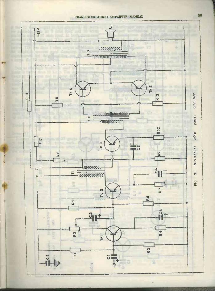
Fig. 31. Newmarket 20 Watt Power AmplifierFor a public address amplifier a power amplifier
of at least 10 watts output is required. Since itmay need to be operated some distance from anymains supply it must consume a minimum ofpower.
CharacteristicsInput sensitivity for 20 watts output 10 mVPower gain 80 dBInput impedance 800 ohmsDistortion at 20 watts output Less than 10%Frequency response
50 c/s to 15 Kc/s (-3 dB)Battery drain no signal 550 mABattery drain full output 3.3 Amps.
Fig. 31.RI 220 K -ohmR2 47 K -ohmR3 15 K -ohmR4 5.6 KohmR5 4.7 K -ohmR6 4.7 K -ohmR7 560 ohms
ClC2C3C4C5C6TrlTr2Tr3Tr4Tr5L.S.
R8 180 ohmsR9 10 ohmsR10 1 ohmR11 330 ohmsR12 3 ohmsR13 470 ohmsR14 33 K -ohm
10 uF 12 V.W. (TSL)10 uF 12 V.W. (TSL)10 uF 12 V.W. (TSL)10 uF 12 V.W. (TSL)1000 uF 12 V.W. (TSL)100 uF 12 V.W. (TSL)V10/15AV10/30AV30/20PV30 /30PV30/30P15 ohms LP312 (TSL)
Transformer specificationT1
Turns ratio 4 : 1
Minimum primary inductance 1.5 HMaximum primary D.C. resistance 30 ohms
Turns RatioMinimum primary inductanceMaximum primary d.c. resistance
Turns Ratio .
Minimum primal vinductance
Maximum primary d.c.resistance
T22 : 1 + 180 mH1 ohm
T31 + 1 : 2.5
32 mH (each section)
0.1 ohm
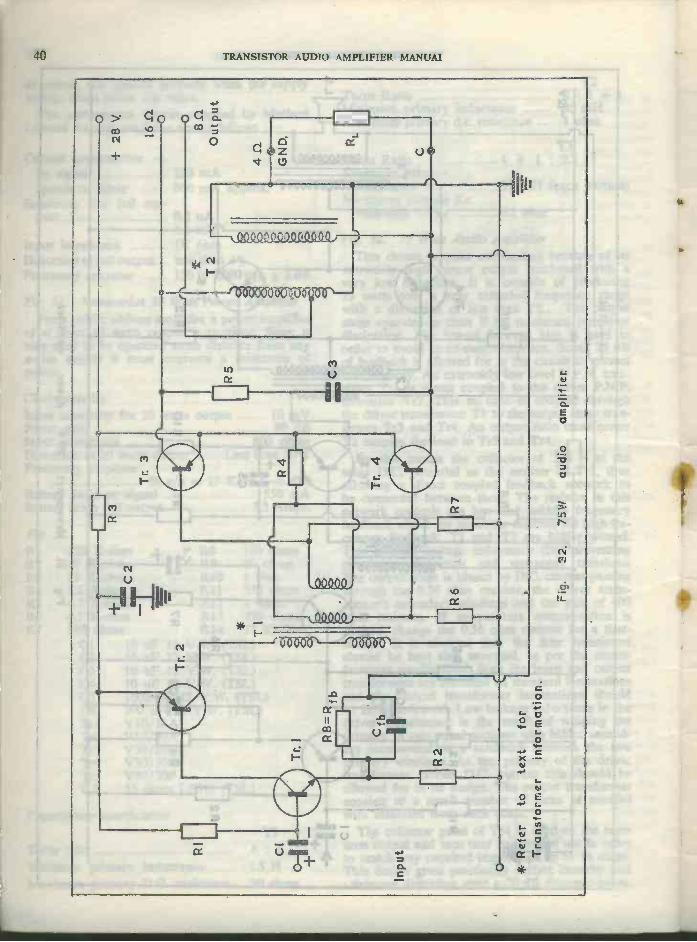
Fig. 32. 75 Watt Audio AmplifierThis circuit is quite outstanding because of its
extremely high power output combined with avery low distortion. It is capable of producing75 watts over a very extended frequency rangewith a distortion of less than 2%. The outputstage operates in class B for minimum transistordissipation. The lowest forward bias is used inorder to avoid cross -over distortion. Some 25 dBof feedback is allowed for in the circuit to correctnon -linearity. An extremely low level N.P.N. tran-sistor Trl is direct coupled to the driver P.N.P.transistor Tr2. This in turn is coupled throughthe driver transformer T1 to the output stage tran-sistors Tr3 and Tr4. An output auto transformerT2 couples the load to Tr3 and Tr4.
By this means the collector of Tr4 is at thesame D.C. potential as the emitter of Trl, thusallowing a direct coupled feedback network tobe connected between them. The resistor in thisnetwork controls the low and middle frequencyfeedback whilst the capacitor controls the high fre-quency feedback. T1 and T2 are bifilar wound.This reduces leakage inductance thus preventingcross -over distortion and unwanted transientsThe output stage is biased by D.C. current passingthrough the 0.56 ohm resistor, the driver trans-former's secondary windings and the pair of 400ohm resistors. If temperature compensation isdesired, change the 0.56 ohm resistor for a ther-mistor. It is obvious that the four transistorsshould be heat sink mounted, as per the manu-facturers specification. Both the input and outputtransformers are mounted on standard laminationsand the output transformer laminations shouldbe full interleaved. Low leakage inductance in thedriver transformer is the result of winding theprimary in two equal sections with bifilar second-ary interwound as a sandwich between the twoprimary windings. As the primary of the drivertransformer carries D.C. current this should beallowed for in its design. The output transformerconsists of a small number of turns of parallelwire insulated from each other.
The collector point of Tr4 is used as the com-mon output and taps may be brought out in orderto match any required impedance up to 16 ohms.This design gives practically perfect linearity andwinimum distortion over a 70 dB dynamic range.
C6 R
I
CI
R2
R3
Tr
I
C2
OM
B
R5
Tr.
2
R6
TI
a
R 8 R9
P
Tr.
3
C5
T2r a a a
0 aco a
a a
a a a 4:
R 1
0
R 1
4
Pit
Tr
4
R12
Fig
.31
.N
ewm
ai-k
et20
Wpo
wer
ampl
ifier
.Tr.
5
I
T 3
c,0 t7
i 6
C.D
0
Tr.
I R8=
Rfb
-II-
Cfb I II
-
R2
Tr.
2
TI
R3
mi,,
C 2
--L-
HII
fee
111.
10M
M.
Tr.
3
R4
e-11 T
r. 4
R6
R7
R5
®C
3
O
+ 2
8 V
.
16 n
.0
T2
08
SI
Out
put
4a
GN
D.
* R
efer
tote
xtfo
rT
rans
form
erin
form
atio
n.
Fig
.32
.75
Wau
dio
ampl
ifier
.
151.
70f3
Sit
TRANSISTOR AUDIO AMPLIFIER MANUAL 41
If the 75 watt output is not required, 40 wattsare available with an 8 ohm load and 20 wattsavailable with a 16 ohm load. In both cases con-nected to the 4 ohm tap. This method of apparentmismatching actually produces very decreased dis-tortion. The less than 1 ohm output impedance ofthe amplifier ensures good damping. The powerrequirements for this amplifier are 28 volts at4 amps. for 75 watt output.
Due to the high feedback used the response islinear to better than 35 Kc/s. The matching impe-dance at the input end is about 48K ohms. Thedesign for this amplifier ensures superb highfidelity quality for large halls and its performancemay be compared most favourably with verylarge valved units.
Using the transformers, details of which arespecified below, the expected performance of thisamplifier is less than 2% distortion, output 60watts at 18 c/s, and less than 2% distortion withan output of 75 watts at 35 c/s.
Transformer design
Driver TlPrimary :- 262 turns of 27 gauge wire wound
in two halves of 131 turns each. One sectionbeneath the secondary and the other section abovethe secondary.
Secondary :- 42 turns bifilar wound 23 gaugewire in a single layer.
Transformer core dimensions :- 14" stack ofL-shaped laminations 1-4.-" size orientated grain.The laminations should be butted without anyspacer in the air gap and not interleaved.
Driver Transformer T2Two parallel bifilar windings of 100 turns layer
wound using 14 gauge wire with a single thicknessof .006" paper in between the layers of wire. Thecore is standard dynamo grade laminations with2" stack L-shaped 14" laminations with a thick-ness of 1/64th of an inch each. The laminationsshould be corn pletely interleaved.
The design of this amplifier is the result oforiginal work by A. B. Bereskin and is describedin the convention record of the American I.R.E.Volume V, 1957 issue.
ComponentsR1 150K ohms Cl 5 microfarads
25 v.w. (TSL)R2 220 ohms C2 1500 microfarads
25 v.w. (TSL)R3 100 ohms C3 0.1 microfaradsR4 0.56 ohms Cfb 0.1 microfaradsR5 100 ohms Trl 2N365 or equivalentR6 400 ohms Tr2 2N352 or 0A70R7 400 ohms Tr3 2N174 or equivalentR8 1.5K ohms Tr4 2N174 or equivalentLS 8 or 16 ohms L P312 (TSL)
42 TRANSISTOR AUDIO AMPLIFIER MANUAL
TECHNICAL SUPPLIERS LIMITEDT'SL type CMS50 loudspeaker
An entirely new design of speaker at extremely low price with great sensitivity and superb
response.
Technical Details.
Diameter - 2"Depth - i"Response - 200-12,000 c/sImpedance - 50-150 ohms
Designed to be connected directly to class A transistor output thus eliminating output trans-formers. Sensitivity is superior to any speaker under 4" diameter, except for models LP45F, LP70and LP31.
LP70 Miniature Speaker High -Q Flexette Sound reproducerA circular unit of extra high sensitivity, function-
ing well from only a quarter of the power requiredto obtain comparable results from larger units,yet it will comfortably handle up to 500 milliwattsloading without signs of distress. Its amazinglywide response ensures quality reproduction fromthe very smallest of sets, making it at least pos-sible to compare pocket-size performance with Specificationthat of top-ranking commercial portables, howeverpowered. Model LP70 is recommended particularlyfor high -quality output portable sets.
Technical DetailsOverall diameter - 21" x 1 1/16" depthResponse - 120-14,500 c/sLoading 4 milliwatts to 500 milliwattsImpedance - 10 ohms
Price: 18s. 8d. + 6s. 4d. P.T. + 8d. surcharge
LP45F Technical SpecificationsOverall diameter - li"Depth - 1"Voice coil impedance - Standard low impedance.Magnet material - FerriteFlux density - 9,500 gaussFrequency response - 120-14,000 c/sLoading - 1 mW to 300 mW
The LP 45F represents a remarkable developmentin the field of small speakers and provides the homeconstructor with a complete new dimension in whichto work. The sensitivity is so high that a clearlyaudible output can be obtained with an input of only1 mW. At the same time the assembly is sufficientlyflexible to permit an input power of 300 mW. Atthis level the output from the speaker, in a suitablecase, is comparable with that obtained from a 4 or5 inch speaker.
The speaker is ideal for use in tiny pocket radiosof the regenerative, reflex or superhet type and ifincorporated in such a set will vastly increase itsperformance. It is, in fact, recommended by CliveSinclair, author of " Practical Transistor Receivers "and numerous other books on transistors.
T.S.L., in offering the LP45F to the home con-structor, guarantees that it is superior to any otherspeaker of this type.
Price: 18s. 8d. + 6s. 4d. P.T. + 8d. surcharge
The world's smallest high fidelity enclosure withsuperb reproduction normally obtainable in enclo-sures at least three times the size.
Cabinet size - 11+" wide x 6-1" high x 74" deep
Frequency range - 45-15,000 c/sPower handling capacity - 4-8 wattsFinish - Highest grade walnut
Price: £4 9s. 2d. + £1 10s. Id. P.T. plus 3s. surcharge
LP312-2 super high fidelity loudspeaker system
This consists of a 12" Lorenz bass and middlerange loudspeaker fitted with 2 LPH65 treble speakerson a bridge across the front of speaker. The resultof this treble speaker system is beyond description.Only the listening ear can convey the superb results.This system is used by many professional broadcast-ing studios for monitor control of their VHF highfidelity broadcast.
Specification
Diameter - 12"Frequency response - 20-17,500 c/sMagnetic - 614 ozs., super ALNICast girder framePower rating - 30 wattsSpeech coil diameter - li"Front to back depth -Baffle opening - 10-1"Output impedance -a choice of 4, 8 or
16 ohms is available on every speaker
Price: £14 19s. 6d. complete(not subject to Purchase Tax)
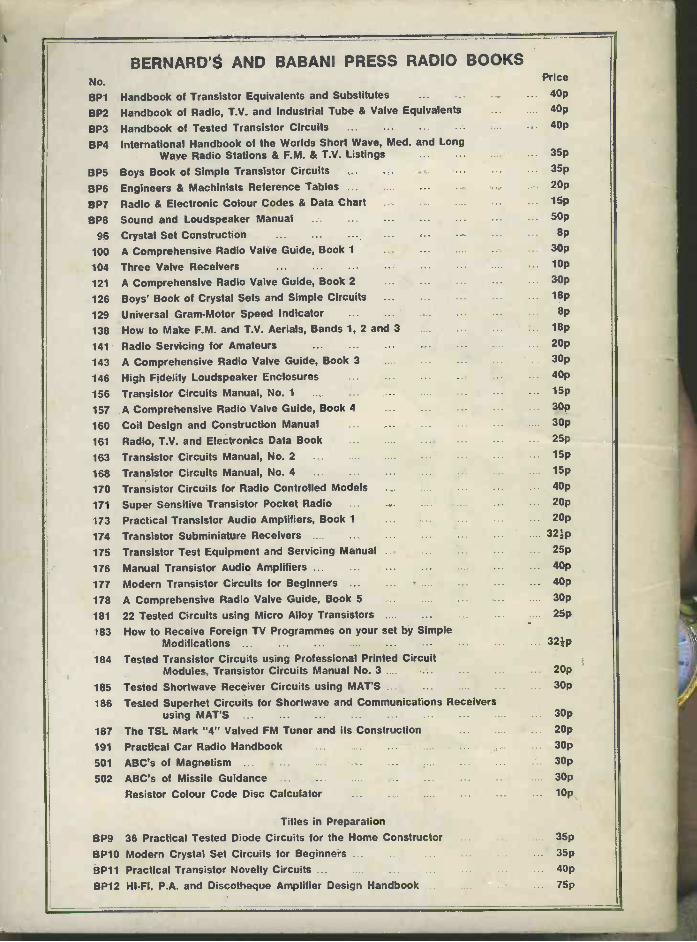
BERNARD'S AND BABANI PRESS RADIO BOOKSNo. Price
BP1 Handbook of Transistor Equivalents and Substitutes 40p
BP2 Handbook of Radio, T.V. and Industrial Tube & Valve Equivalents 40p
BP3 Handbook of Tested Transistor Circuits ... 40p
BP4 International Handbook of the Worlds Short Wave, Med. and LongWave Radio Stations & F.M. & T.V. Listings 35p
BP5 Boys Book of Simple Transistor Circuits ... 35p
BP6 Engineers & Machinists Reference Tables ... 20p
BP7 Radio & Electronic Colour Codes & Data Chart 15p
BPB Sound and Loudspeaker Manual 50p
96 Crystal Set Construction 8p
100 A Comprehensive Radio Valve Guide, Book 1 30p
104 Three Valve Receivers 10p
121 A Comprehensive Radio Valve Guide, Book 2 30p
126 Boys' Book of Crystal Sets and Simple Circuits 18p
129 Universal Gram -Motor Speed Indicator 8p
138 How to Make F.M. and T.V. Aerials, Bands 1, 2 and 3 18p
141 Radio Servicing for Amateurs 20p
143 A Comprehensive Radio Valve Guide, Book 3 30p
146 High Fidelity Loudspeaker Enclosures 40p
156 Transistor Circuits Manual, No. 1 15p
157 A Comprehensive Radio Valve Guide, Book 4 30p
160 Coil Design and Construction Manual 30p
161 Radio, T.V. and Electronics Data Book 25p
163 Transistor Circuits Manual, No. 2 15p
168 Transistor Circuits Manual, No. 4 15p
170 Transistor Circuits for Radio Controlled Models 40p
171 Super Sensitive Transistor Pocket Radio 20p
173 Practical Transistor Audio Amplifiers, Book 1 20p
174 Transistor Subminiature Receivers 321p
175 Transistor Test Equipment and Servicing Manual 25p
176 Manual Transistor Audio Amplifiers ... 40p
177 Modern Transistor Circuits for Beginners 40p
178 A Comprehensive Radio Valve Guide, Book 5 30p
181 22 Tested Circuits using Micro Alloy Transistors .... 25p
183 How to Receive Foreign TV Programmes on your set by SimpleModifications . . 321p
184 Tested Transistor Circuits using Professional Printed CircuitModules, Transistor Circuits Manual No. 3 20p
185 Tested Shortwave Receiver Circuits using MAT'S 30p
186 Tested Superhet Circuits for Shortwave and Communications Receiversusing MAT'S 30p
187 The TSL Mark "4" Valved FM Tuner and its Construction 20p
191 Practical Car Radio Handbook 30p
501 ABC's of Magnetism 30p
502 ABC's of Missile Guidance 30p
Resistor Colour Code Disc Calculator 10p
Titles in Preparation
9139 36 Practical Tested Diode Circuits for the Home Constructor 35p
BP10 Modern Crystal Set Circuits for Beginners 35p
BP11 Practical Transistor Novelty Circuits 40p
BP12 HI-FI, P.A. and Discotheque Amplifier Design Handbook 75p


![RF Circuit Design - [Ch4-1] Microwave Transistor Amplifier](https://img.pdfslide.us/doc/110x75/55cc6094bb61eb9d338b474f/rf-circuit-design-ch4-1-microwave-transistor-amplifier.jpg)