Embed Size (px)
Citation preview
AU/ComputerOrganizationAndArchi/Lecture_1
1
Adama UniversityFaculty of Technology and IT
Department of Electrical Engineering Computer Organization and Architecture
• Introduction to Digital Systems• Number Systems• Digital Logics• Microprocessor and microcomputers • Evolution of microprocessors• Embedded microcontrollers and Bit splice processors
AU/ComputerOrganizationAndArchi/Lecture_1
2
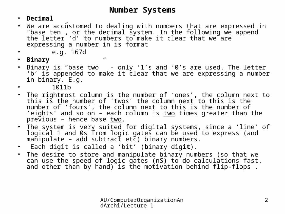
Number Systems• Decimal• We are accustomed to dealing with numbers that are expressed in “base
ten”, or the decimal system. In the following we append the letter ‘d’ to numbers to make it clear that we are expressing a number in is format
• e.g. 167d• Binary• Binary is “base two” - only ‘1’s and ‘0’s are used. The letter ‘b’ is appended
to make it clear that we are expressing a number in binary. E.g.• 1011b• The rightmost column is the number of ‘ones’, the column next to this is the
number of ‘twos’ the column next to this is the number of ‘fours’, the column next to this is the number of ‘eights’ and so on – each column is two times greater than the previous – hence base two.
• The system is very suited for digital systems, since a ‘line’ of logical 1 and 0s from logic gates can be used to express (and manipulate – add subtract etc) binary numbers.
• Each digit is called a ‘bit’ (binary digit). • The desire to store and manipulate binary numbers (so that we can use the
speed of logic gates (nS) to do calculations fast, and other than by hand) is the motivation behind flip-flops .
AU/ComputerOrganizationAndArchi/Lecture_1
3
Number Systems
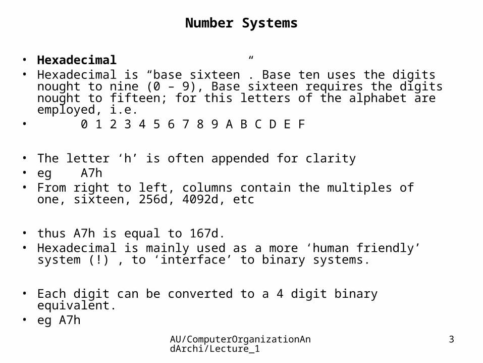
• Hexadecimal• Hexadecimal is “base sixteen”. Base ten uses the digits nought to
nine (0 – 9), Base sixteen requires the digits nought to fifteen; for this letters of the alphabet are employed, i.e.
• 0 1 2 3 4 5 6 7 8 9 A B C D E F
• The letter ‘h’ is often appended for clarity• eg A7h• From right to left, columns contain the multiples of one, sixteen,
256d, 4092d, etc
• thus A7h is equal to 167d.• Hexadecimal is mainly used as a more ‘human friendly’ system (!) ,
to ‘interface’ to binary systems.
• Each digit can be converted to a 4 digit binary equivalent.• eg A7h
AU/ComputerOrganizationAndArchi/Lecture_1
4
Number Systems
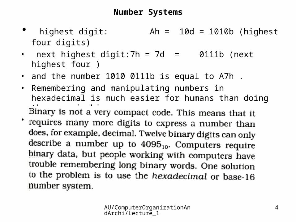
• highest digit: Ah = 10d = 1010b (highest four digits)
• next highest digit:7h = 7d = 0111b (next highest four )• and the number 1010 0111b is equal to A7h .• Remembering and manipulating numbers in hexadecimal is much
easier for humans than doing the same in binary. • This becomes clear when dealing with microprocessors at a system-
level .

AU/ComputerOrganizationAndArchi/Lecture_1
5
Number Systems
AU/ComputerOrganizationAndArchi/Lecture_1
6
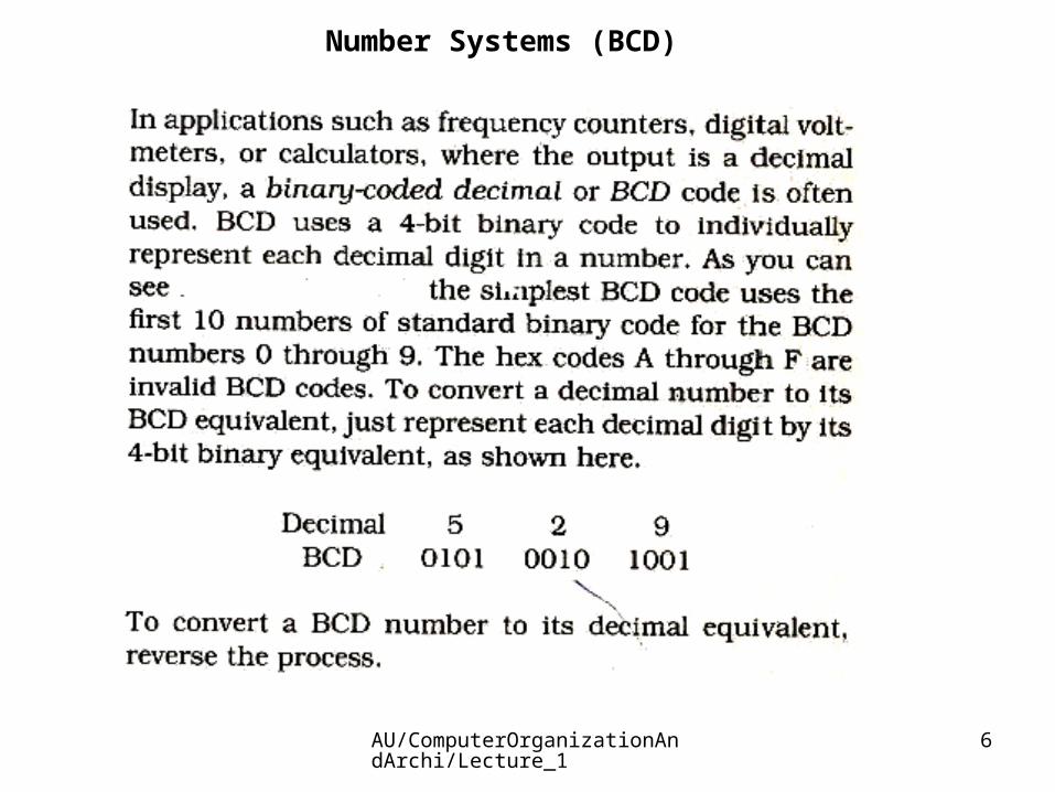
Number Systems (BCD)

AU/ComputerOrganizationAndArchi/Lecture_1
7
Number Systems (BCD)

AU/ComputerOrganizationAndArchi/Lecture_1
8
Logic Gates
• Logic• In engineering sense: representation of switching circuits using
digital electronics. eg circuitry to implement: if lights are on, and door is open, then sound buzzer
• each precondition has two states: True or False – suited to logic• Two types of logic:• –Combinatorial logic – switching circuit produces output at instant
predetermined combination of input conditions occur – e.g. burglar alarms, lights-on warning buzzers
• –Sequential logic – output is dependent on sequence of events which has already occurred in system – i.e. counters, automatic tool control systems, microprocessors
• Combinatorial Logic• This uses devices known as logic gates to provide 3 basic logic
operations• - AND• - OR• - NOT• These can be combined to give other standard gates such as NAND
(Not And).

AU/ComputerOrganizationAndArchi/Lecture_1
9
Logic Gates• NOT Gate• A NOT gate outputs a logic state which is the opposite of the input • AND gate• The output is high only if all inputs are high • NAND gate• The NAND (Not And) gate could be made by negating the output of an
AND gate using a not gate. The output is low only if all inputs are high:

AU/ComputerOrganizationAndArchi/Lecture_1
10
Logic Gates• OR gate• Output is high if either or both inputs are high• Lastly we have the XOR (exclusively Or). The output is high if A or B
is high, but not if both are high.

AU/ComputerOrganizationAndArchi/Lecture_1
11
Latches
.
AU/ComputerOrganizationAndArchi/Lecture_1
12
Latches
AU/ComputerOrganizationAndArchi/Lecture_1
13
Flip-flops
AU/ComputerOrganizationAndArchi/Lecture_1
14
Flip-flops

AU/ComputerOrganizationAndArchi/Lecture_1
15
Registers
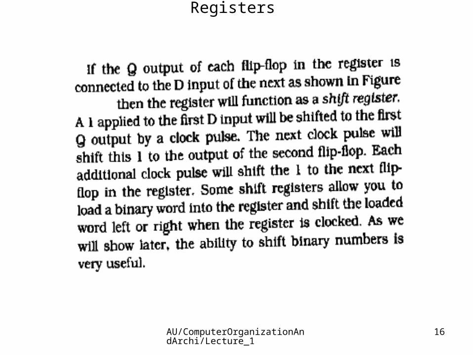
AU/ComputerOrganizationAndArchi/Lecture_1
16
Registers
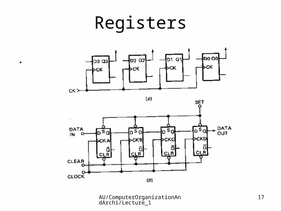
AU/ComputerOrganizationAndArchi/Lecture_1
17
Registers
.

AU/ComputerOrganizationAndArchi/Lecture_1
18
.
Counters
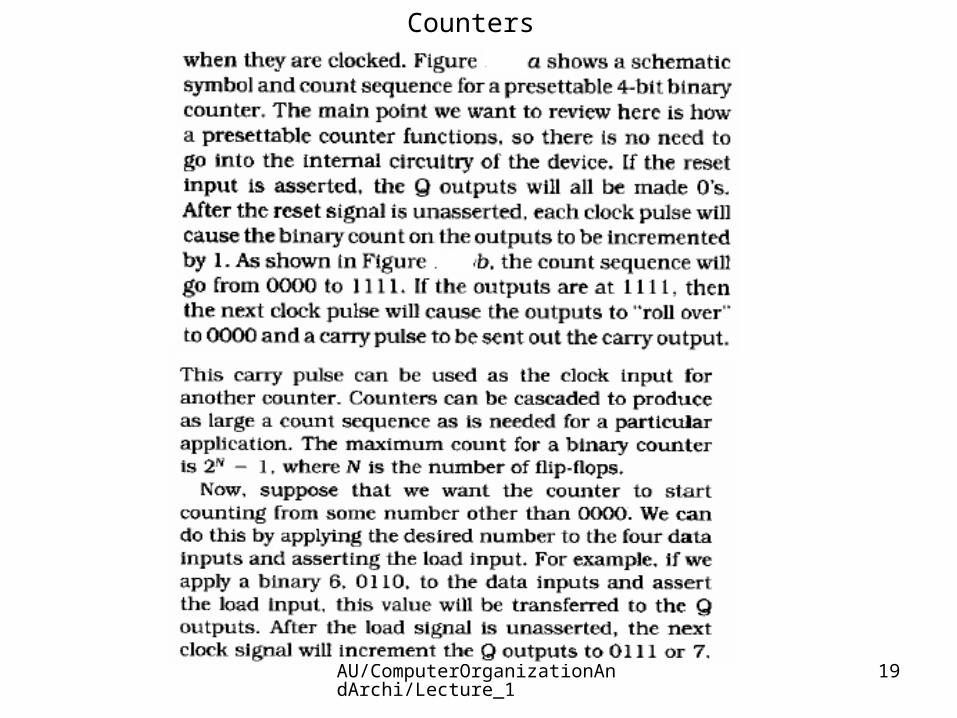
AU/ComputerOrganizationAndArchi/Lecture_1
19
Counters
AU/ComputerOrganizationAndArchi/Lecture_1
20
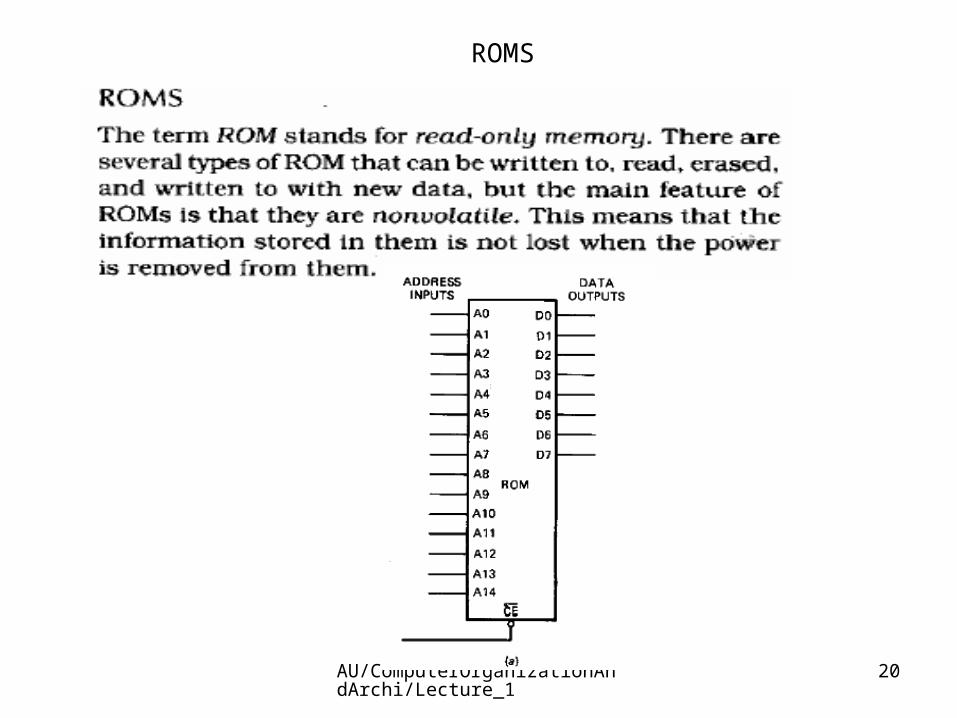
ROMS
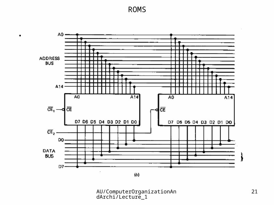
AU/ComputerOrganizationAndArchi/Lecture_1
21
.
ROMS
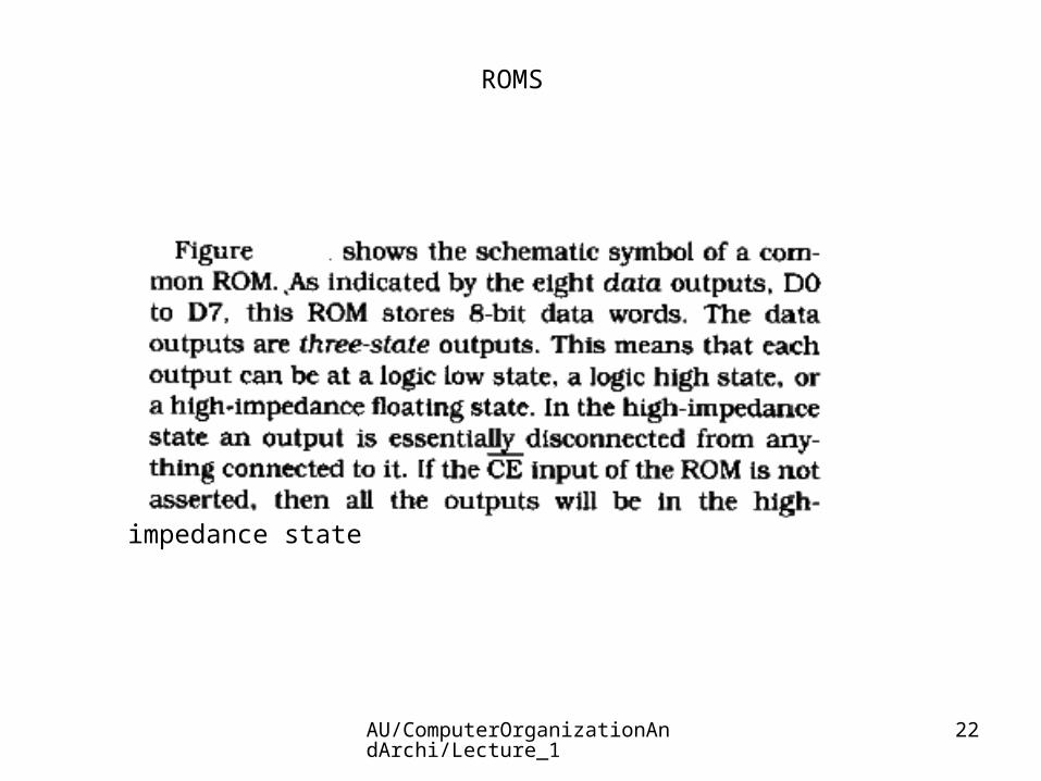
AU/ComputerOrganizationAndArchi/Lecture_1
22
ROMS
impedance state

AU/ComputerOrganizationAndArchi/Lecture_1
23
Microprocessor
Definition:• Microprocessor is a single IC chip that is able to compute, to be
programmed and is able to receive and send out data to an external device.
• It is very difficult to find an application, electronic system, where the microprocessor is not used.
• It is the single IC that tremendously affected the life style of people all over the world.
• It is used as CPU in computer systems, CRT terminals, telephone switching networks, DSP in entertainment devices, television tuning and even in digital voltmeters, oscilloscopes, vehicles, appliances, cameras, wireless devices, industrial control systems etc. Today’s cars alone probably use at least 40 or 50 microprocessors.
AU/ComputerOrganizationAndArchi/Lecture_1
24
History of microprocessors • In the early 1970s, integrated circuit manufacturers had a
problem. Technology available to build complex chips vary cheaply in high volume, none of the markets they had were big enough to provide the volume of sales required - these were Telecom, Mainframe and Mini Computers, Consumer Electronics.
• What was needed was a very general-purpose system which could be customized after manufacture to the application area.
• Hence the Solution: Since computers were "general purpose" by definition, the idea hit upon was to build components for very primitive computers.
• Intel Corporation was first, with a chip set, called the 4004, for a family of calculators. By current standards, this set was very slow, and was soon replaced by the 4040 which was a little better.
• The first microprocessor of note was the Intel 8008, which could handle data 8 bits at a time.
• This was followed by Motorola with their 6800, and Intel shortly thereafter brought out the 8080. These two µPs established the market and have dominated it for many years.
AU/ComputerOrganizationAndArchi/Lecture_1
25
History of microprocessors
• Microprocessors consist of many internal components but they also need some external components to operate as a complete system.
• Internally it consists of registers, which are serially connected flip flops used as data storage units, buses and components that are used to control and process arithmetic and logical operations.
• The arrangement of these components is what is referred as architecture.
• Following diagram shows a general arrangement of these components.

AU/ComputerOrganizationAndArchi/Lecture_1
26
• Figure
Internal buss address , data and control
Stack pointer Accumulator
Program counter ALU
Instruction Register Flag resister
Operation control and timings Circuit General purpose
Register
RAM
ROM
Buffer
Circuits
Clock
AU/ComputerOrganizationAndArchi/Lecture_1
27
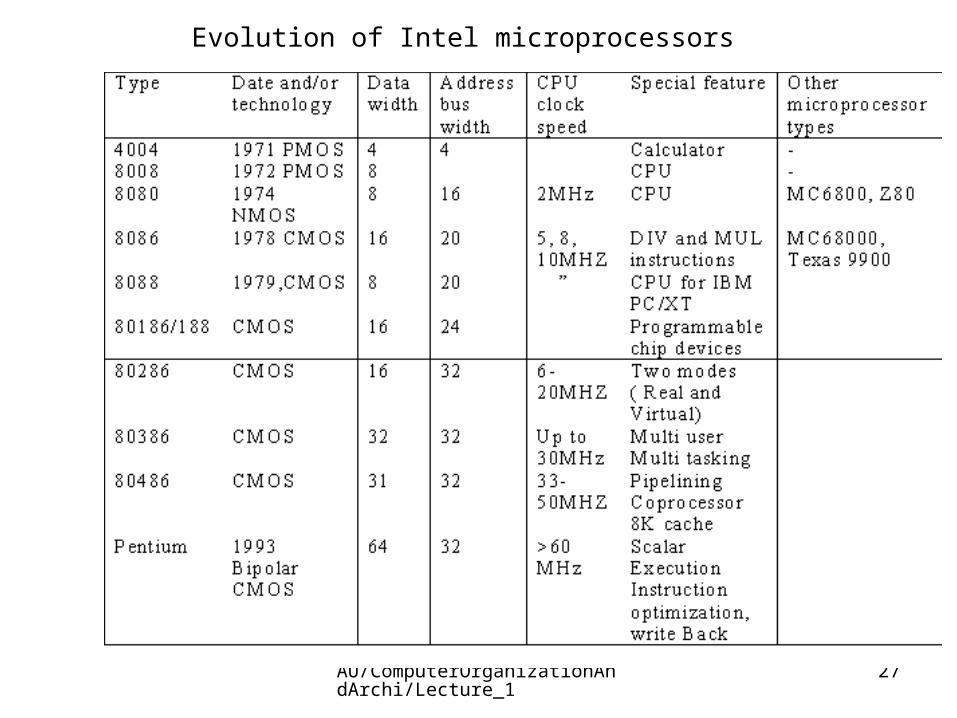
Evolution of Intel microprocessors
AU/ComputerOrganizationAndArchi/Lecture_1
28
Evolution of Intel microprocessors
• In recent microprocessor industry, Intel, Motorola, Advanced Micro Devices ( AMD), IBM, Sun Microsystems and Hewlett Packard are the well known manufacturers and are striving to manufacture the most powerful 32 or 64 bit processors.
• After the first Pentium processor, Intel has released processors named as Pentium Pro, Pentium MMX, Pentium II, Pentium III and IV.
AU/ComputerOrganizationAndArchi/Lecture_1
29
Classification of processors
• 1.Embedded controllers – These are VLSI chips which are basically designed for control system applications.
• They differ from the general purpose microprocessors in that they consist of RAM, ROM and some I/O ports with in a single chip in addition to the main CPU.
• Examples are Intel 8048, Intel 8031 and 8051
• 2.Bit slice processors – These are small processors used for custom building of higher speed and performance specific applications.
• The units consist of ALU, multiplexers and other parts. Then one will use these basic units to build a customized processor using the basic elements.
• 3.General Purpose processors- these are high end processors that are used for computers.
AU/ComputerOrganizationAndArchi/Lecture_1
30
Basic Architectural Features of 8086 • The 8086 is the first 16 bit microprocessor of the Intel family. It is
40 pin IC with DIP package manufactured using the CMOS technology.
• 1. External Hardware features of 8086• a) It has :• Pin 1,20 are Ground • Pin 40 Vcc• Pin 2- 16,39 are time multiplexed address and data lines, AD0
to AD14 and AD15 • Pin 35-38 are also time multiplexed Address/status lines• Pin 19 clock with 33% duty cycle. There are three types of 8086
processors regarding their clock speeds, 5, 8 and 10MHz. • Other pins are control pins. • b) DC and AC characteristics – The DC and AC characteristics
of the processor are included from the manufacturers data sheet. • The processor needs only one power supply, unlike its
predecessors that need the 5V. The currently available Intel Pentium processors require additional power of, +3.3V.
AU/ComputerOrganizationAndArchi/Lecture_1
31
Internal Architectural features
• The basic operations of any microprocessor can be divided into three. These are
• a) Instruction fetching – reading an instruction from memory into the internal system
• b) Instruction Decoding – interpreting the meaning of the instruction and generating micro instructions
• c) Instruction Execution- performing the microinstructions • The whole operation of a microprocessor is controlled and
governed by a clock.
• The above three main operations of a microprocessor are performed by different system components. Following is a block diagram showing the internal architecture of the 8086
microprocessor.

AU/ComputerOrganizationAndArchi/Lecture_1
32

AU/ComputerOrganizationAndArchi/Lecture_1
33
Internal Architectural features
• As it is indicated in the block diagram, the main components that are included as internal elements are buses and registers with associated control and timing circuits.
• The components can be classified into two functional units: execution unit and bus interface unit
• a) The execution unit- consist of ALU, general purpose registers, flag registers, and the instruction decoder.
• The main purpose of this unit is decoding and instruction execution.
• The ALU is responsible to perform arithmetic and logical operations. Before any arithmetic or logical operation is performed, the operands ( i.e. data to be manipulated) should have to be brought from memory and stored in registers.
• The width of the ALU is critical in determining the speed of the processor, because the wider the ALU, the higher will be the number of bits that could be manipulated at a time and it increases the speed of the processor.
AU/ComputerOrganizationAndArchi/Lecture_1
34
Internal Architectural features
• The 4 general purpose registers are named as AX, BX, CX and DX.• They can be used as 8 bit registers by referring to their lower and higher
byte as AL and AH and so on. In 8080 and 8085 processors, the AX register was having a special name known as accumulator and was the only register involved in arithmetic and logical instructions.
• But in 8086 any one of the registers can be used. • The instruction decoder, some times referred as instruction register, is
the destination for all op codes. • When an instruction is fetched, its first byte, i.e. op code is sent to the
instruction decoder and then the decoder generates micro instructions or control signals that are used to control and guide the execution of the particular instruction.
• The processor determines the number of operands needed, or whether the instruction is jump or not etc only after the instruction is decoded.
• The flag register is a special register used to save the status of the result of arithmetic and logical instructions. After an arithmetic or logical instruction is performed by the ALU, the result is stored in the general purpose registers.

AU/ComputerOrganizationAndArchi/Lecture_1
35
Internal Architectural features
• OF Overflow flag, is set if the width of register is less than result of calculation. It is mostly affected when multiplication is performed.
• DF String direction flag, determines the direction of movement of string
• IF Interrupt enable flag, is set if the processor is able to accept interrupts.
• TF single step trap flag • SF sign flag determines if result of calculation is zero or not.• ZF, zero flag is set if the result is zero. • AF Auxiliary flag used in BCD calculation. It keeps track of the
carry over to the 4 bit from a 4th. It is set to when there is a carry. • PF parity flag, checks the number of 1’s with in the bit sequence
and/or move• CF carry flag• U is undefined bit
AU/ComputerOrganizationAndArchi/Lecture_1
36
Internal Architectural features
• b) The bus interface unit – consists of segment registers, instruction pointer, adder and queue. This unit is responsible for fetching instruction and data from memory.
• Segment Registers – As shown in the block diagram above, the 8086 has four segment registers. Code segment, Data segment, Extra segment and Stack segments.
• These segment registers are used to hold the upper 16 bits of the base value for the different memory sections. The 8086 can address a total of 1M bytes of memory but because of the 16 bit internal register limitation, it can work with only four 64K byte memory segments at a time.
• The part of memory that is active at any one time is determined by the content of the four segment registers.
• Instruction Pointer- is a 16 bit register used to hold the offset address value of a data or a code from the base value with in a segment.
• Hence at any one time, the actual 20 bit memory address is generated by the BIU using segment register and the instruction pointer.
• 20 bit address = (segment register)*16 + IP• Multiplication by 16 is achieved by shifting the code segment bits to the
left 4 bits.

AU/ComputerOrganizationAndArchi/Lecture_1
37
Internal Architectural features• The Instruction Pointer (IP) and Address Summation: The IP contains
the Offset Address of the next instruction, which is the distance in bytes from the base address given by the current Code Segment (CS) register. The figure shows how this is done.
• The contents of the CS are shifted left by four. Bit 15 moves to the Bit 19 position. The lowest four bits are filled with zeros. The resulting value is added to the Instruction Pointer contents to make up a 20-bit physical address. The CS makes up a segment base address and the IP is looked as an offset into this segment.
• This segmented model also applies to all the other general registers and segment registers in the 8086 device. For example, the SS and SP are combined in the same way to address the stack area in physical memory.
AU/ComputerOrganizationAndArchi/Lecture_1
38
Internal Architectural features
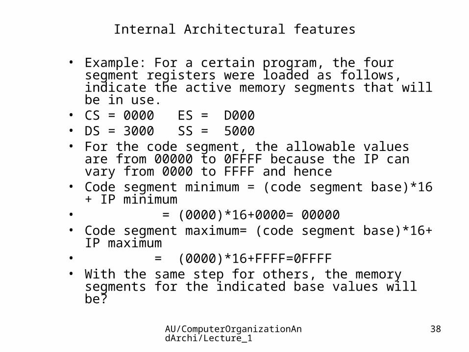
• Example: For a certain program, the four segment registers were loaded as follows, indicate the active memory segments that will be in use.
• CS = 0000 ES = D000 • DS = 3000 SS = 5000• For the code segment, the allowable values are from 00000
to 0FFFF because the IP can vary from 0000 to FFFF and hence
• Code segment minimum = (code segment base)*16 + IP minimum
• = (0000)*16+0000= 00000• Code segment maximum= (code segment base)*16+ IP
maximum • = (0000)*16+FFFF=0FFFF• With the same step for others, the memory segments for the
indicated base values will be?