Embed Size (px)
Citation preview

AUDIO
352/2002 Elektor Electronics
If we compare these two power amplifierICs, the first thing that strikes us is the simi-larity of their internal circuitry and externalwiring (see Figure 1). Two small but importantdifferences allow the new IC amplifier to be
The Variable Final Amplifier is builtusing ST Microelectronics TDA7293ICs, which have MOS outputs stages.This integrated power amplifier IC isa successor to the TDA7294, whichwas described a long time ago in anElektor Electronics data sheet (May1993) based on an SGS Thomsonproduct announcement. EvidentlySGS Thomson experienced difficultiesin the development of this IC, since ittook three full years until the IC
appeared on the market. However, atthe end of 1996 it was ready, and itwas used in the 50-W A.F. Amplifier(November 1996 issue), which hasbeen built by many hobbyists.
VersatileFinal Amplifieraudio power with many featuresBy U. Böhmke Internet: www.ub-elektronik.de
e-mail: [email protected]
Only a few years ago, many music lovers turned up their noses on seeing ahybrid circuit or integrated circuit in a final amplifier, but now there is a newgeneration of outputstage ICs that havebeen specially designedfor use in high-quality audioamplifiers.
used much more flexibly: first, the connectionbetween the input and output stages can beopened to allow the output stage to be drivenexternally, and secondly there is a specialcharging output for the bootstrap capacitor.We will see what these features allow us to do.
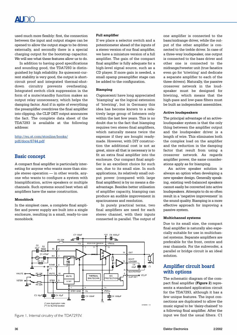
In addition to having good specificationsand sounding good, the TDA7293 is distin-guished by high reliability. Its quiescent-cur-rent stability is very good, the output is short-circuit proof and integrated thermal-shut-down circuitry prevents overheating.Integrated switch click suppression in theform of a mute/standby function makes anoutput relay unnecessary, which helps thedamping factor. And if in spite of everythingthe preamplifier overdrives the final amplifierinto clipping, the CLIP DET output announcesthe fact. The complete data sheet of theTDA7293 is available at the followingaddress:
http://eu.st.com/stonline/books/pdf/docs/6744.pdf
Basic conceptA compact final amplifier is particularly inter-esting for anyone who wants more than sim-ple stereo operation — in other words, any-one who wants to configure a system withbiamplification, active speakers or multiplechannels. Such systems sound best when allamplifiers have the same construction.
Monoblock
In the simplest case, a complete final ampli-fier and power supply are built into a singleenclosure, resulting in a small, ready-to-usemonoblock.
Full amplifierIf we place a selector switch and apotentiometer ahead of the inputs ofa stereo version of our final amplifier,we have a miniature version of a fullamplifier. The gain of the compactfinal amplifier is fully adequate for ahigh-level signal source, such as aCD player. If more gain is needed, asmall opamp preamplifier stage canbe added to the configuration.
Biamping
Cognoscenti have long appreciated‘biamping’ as the logical extensionof ‘biwiring’, but in Germany thisidea has become known to a rela-tively large group of listeners onlywithin the last few years. This is nodoubt due to the fact that biampingrequires two stereo final amplifiers,which naturally means twice theexpense if they are bought ready-made. However, with DIY construc-tion the additional cost is not asgreat, since all that is necessary is tofit an extra final amplifier into theenclosure. Our compact final ampli-fier is an excellent choice for suchuse, due to its small size. In suchapplications, its relatively small out-put power (compared with largefinal amplifiers) is by no means a dis-advantage. Besides better utilisationof amplifier capacity, biamping canproduce an audible improvement inspaciousness and resolution.
In purely practical terms, twofinal amplifiers are need for eachstereo channel, with their inputsconnected in parallel. The output of
one amplifier is connected to thebass/midrange driver, while the out-put of the other amplifier is con-nected to the treble driver. In case ofa three-way loudspeaker, one outputis connected to the bass driver andother one is connected to themidrange/tweeter unit (true fanaticseven go for ‘triwiring’ and dedicatea separate amplifier to each of thethree drivers). Naturally, the passivecrossover network in the loud-speaker must be designed forbiwiring, which means that thehigh-pass and low-pass filters mustbe built as independent assemblies.
Active loudspeakers
The principal advantage of an active-loudspeaker system is that the onlything between the amplifier outputand the loudspeaker driver is alength of wire. This eliminates boththe complex load on the amplifierand the reduction in the dampingfactor that result from using acrossover network. As regardsamplifier power, the same consider-ations apply as for biamping.
An active speaker solution isalways an option when developing anew speaker design. Generally speak-ing, existing well-balanced speakerscannot easily be converted into activeloudspeakers. Attempts to do so oftenresult in a ‘negative improvement’ inthe sound quality. Biamping is a moreeffective approach for improving apassive system.
Multichannel systems
Due to its small size, the compactfinal amplifier is naturally also espe-cially suitable for use in multichan-nel systems. Separate amplifiers arepreferable for the front, centre andrear channels. For the subwoofer, aparallel or bridge circuit is an idealsolution.
Amplifier circuit board with optionsThe schematic diagram of the com-pact final amplifier (Figure 2) repre-sents a standard application circuitfor the TDA7293, although it has afew unique features. The input con-nections are duplicated to allow themusic signal to be ‘daisy-chained’ toa following final amplifier. After theinput we find the usual filters. C1
AUDIO
36 Elektor Electronics 2/2002
Figure 1. Internal circuitry of the TDA7293V.

tages, particularly with load impedances lessthan 8 Ω, and is the only manner in which a2-Ω load can be driven. With a 4-Ω load, thesupply voltage can be raised to the 8-Ω level,with the result that the output power can beincreased to more than 100 W.
In bridge operation, one amplifier worksagainst the output of a second, invertingamplifier instead of against ground. Theoret-ically, this doubling of the output voltageswing results in quadrupling the outputpower into a 4-Ω load. However, the loud-speaker must have an impedance of at least8 Ω, due to thermal considerations, so onlyhalf of this theoretical increase can actuallybe realised, but that is still good for up to150 W (depending on the quality of the powersupply). The damping factor is reduced by afactor of 2 relative to a single amplifier drivingan 8-Ω load.
The component connected to pins 1, 9 and10 provide switch click suppression. The
and R3 form an input high-pass filterthat isolates the input from any dcvoltage present at the output of theprevious stage.
The TDA7293 can be seen as anon-inverting operational amplifier.The gain is set to around 35 by thenegative feedback network. Thisamount of gain results in the bestbalance of speed, bandwidth andstability. In order to avoid amplifyingthe input offset voltage, the amplifieris ac coupled. Capacitor C6 improvesthe square-wave response.
Good-quality components mustbe used for the Boucherot network(R7 / C15). R7 must be a low-induc-tance type, while a foil capacitormust unconditionally be used forC15.
Although it is possible to obtainmore output power by operating twomodules in parallel (for a 2-Ω or 4-Ω
load) or in a bridge configuration (foran 8-Ω load), the TDA7293 gives thebest results (in terms of both mea-surements and listening tests) whenused alone. Consequently, paralleland bridge configurations should beused only for subwoofers.
If only a single amplifier moduleis used, the load impedance shouldnot be less than 4 Ω. Since the pro-tective circuitry cannot cope withextremely low-impedance or com-plex loads (such as the InfinityKappa), the amplifier will bedestroyed!
However, two amplifiers can eas-ily be connected in parallel. Thepower dissipation is then dividedover two packages and can thus begreater than with a single module.The internal resistance drops in pro-portion to the number of modulesused. This yields certain advan-
AUDIO
372/2002 Elektor Electronics
R1
390Ω
R10
100k
R8
24k
R9
47k
R2
24
k
C1
1µ
C2
470p
1 2
3 4
5 6
7 8
9 10
K2
1 2
3 4
5 6
7 8
9 10
K1
JP1
K4
JP3JP2
C13
10µ63VC14
D11N4148
C8
47µ
C7
47µ
BOOTSTRAP
TDA7293
STBYGND –PWVS
+PWVS
SGND
IC1
MUTE
STBY
CLIP
OUT
–VS
IN–
IN+
+VS
14
15
10
13
BD11
BL12
6
81
2
3
4
9
7
5
K3
K6
K5
+UB
+UB
R6
100k
R5
24k
R4
560Ω
R3
19
k6
(20k)
C9
1000µ63V
C11
150n
C10
1000µ63V
C12
150n
R7
2Ω
2
C15
100n
C6
22p*
C5
100n
C3 C4100µ25V
2x
2x
NORMAL
PAR/SLAVE
AMP
LSP
– UB
B+ U
010049 - 11
zie tekst*siehe Text*see text*
voir texte*
S1
on
off
*
*
50V
50V
S M
PARALLEL
Figure 2. The circuit diagram of the amplifier corresponds to the standard application but has a number of special configuration options.
AUDIO
38 Elektor Electronics 2/2002
010049-1
(C) ELEKTOR
C1
C2
C3C4
C5C6
C7
C8
C9C10
C11
C12
C13C
14
C15
D1
H1
H2H3
H4
IC1
JP1
JP2JP3
K1
K2
K3
K4
K5K6
OU
T
R1R2
R3R4
R5R6
R7
R8
R9R10
T
T
010049-1
TTT
+UB
M
S
-UB
LSP
S1 off on
01
00
49
-1(C
) ELE
KTO
R
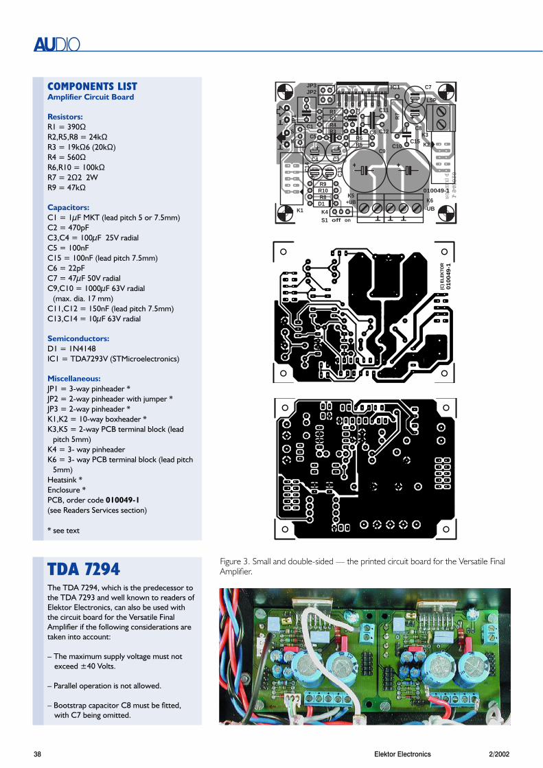
Figure 3. Small and double-sided — the printed circuit board for the Versatile FinalAmplifier.
COMPONENTS LISTAmplifier Circuit Board
Resistors:R1 = 390ΩR2,R5,R8 = 24kΩR3 = 19kΩ6 (20kΩ)R4 = 560ΩR6,R10 = 100kΩR7 = 2Ω2 2WR9 = 47kΩ
Capacitors:C1 = 1µF MKT (lead pitch 5 or 7.5mm)C2 = 470pFC3,C4 = 100µF 25V radialC5 = 100nFC15 = 100nF (lead pitch 7.5mm)C6 = 22pFC7 = 47µF 50V radialC9,C10 = 1000µF 63V radial
(max. dia. 17 mm)C11,C12 = 150nF (lead pitch 7.5mm)C13,C14 = 10µF 63V radial
Semiconductors:D1 = 1N4148IC1 = TDA7293V (STMicroelectronics)
Miscellaneous:JP1 = 3-way pinheader *JP2 = 2-way pinheader with jumper *JP3 = 2-way pinheader *K1,K2 = 10-way boxheader *K3,K5 = 2-way PCB terminal block (lead
pitch 5mm)K4 = 3- way pinheaderK6 = 3- way PCB terminal block (lead pitch
5mm)Heatsink *Enclosure *PCB, order code 010049-1(see Readers Services section)
* see text
TDA 7294The TDA 7294, which is the predecessor tothe TDA 7293 and well known to readers ofElektor Electronics, can also be used withthe circuit board for the Versatile FinalAmplifier if the following considerations aretaken into account:
– The maximum supply voltage must notexceed ±40 Volts.
– Parallel operation is not allowed.
– Bootstrap capacitor C8 must be fitted,with C7 being omitted.

AUDIO
392/2002 Elektor Electronics
only 0.5 mA.Naturally, if several amplifiers are con-
nected to a common power supply (forbiamping, active loudspeakers, parallel oper-ation or bridge operation), this functionshould be controlled using a single commonswitch. This can be achieved by using 10-way flat cable to interconnect the K1 connec-tors of the individual amplifiers, which isalready the case for parallel and bridge con-figurations.
Caution:This must only be done with final amplifiersthat are powered from a single commonpower supply!
selector switch (S1) is connected toconnector K4. When S1 is switchedto the supply voltage, the TDA7293awakens from the standby modeafter a brief delay, and shortly there-
after the mute circuit activates theoutput. If S1 is switched to ground,the output is first muted and thenthe IC goes into the standby mode,in which its current consumption is
NormalBridge mode Parallel mode
JP1
JP2
JP3
PC1,2
Master Slave Master Slave
open
installed
open
input
to M
installed
open
input
to S
installed
open
bridge
open open
open
open
open
input
installed
installed
Figure 4. A classic design, but with fast rectifier diodes instead of a bridge module — the power supply for the Versatile Final Amplifier.
R1
0Ω15
5W
R2
0Ω15
5W
R3
0Ω15
5W
R4
0Ω15
5W
D1
C1 47n
D2
C2 47n
D3
C3 47n
D4
C4 47n
R7
12
k
D5
POWER
C5
3µ3
C6
3µ3
C11
3µ3
C12
3µ3
C7 C9
C8 C10
R5
4k
7
R6
4k
7
K2
K1
K5
K4
K3
K10
K9
K6
K7
K8
010049 - 12
D1 ... D4 = BYV29-200
C7 ... C10 = 10 000µF / 63V
Tr1
– UB
B+ U
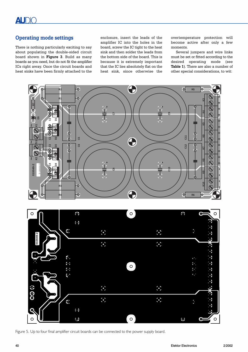
COMPONENTS LISTPower Supply(depending on number of final amplifiers)
Resistors:R1-R4 = 0Ω15 5WR5,R6 = 4kΩ7R7 = 12kΩ
Capacitors:C1-C4 = 47nF ceramic
C5,C6,C11,C12 = 3µF3 250VDC /160VAC MKT (size 11x21x31.5mm)(e.g., Epcos B32524-Q3335-K, Farnell# 331-3311)
C7-C10 = 10,000 µF 63V radial, leadpitch 10mm, max. dia. 45mm), PCBmount
Semiconductors:D1-D4 = BYV29-200D5 = high efficiency LED
Miscellaneous:K1-K10 = 2-way PCB terminal block
(lead pitch 5mm)Mains transformer, 2 x 22V at 225VAPCB, order code 010049-2
(see Readers Services section)
Table 1: Jumper settings
Operating mode settings
There is nothing particularly exciting to sayabout populating the double-sided circuitboard shown in Figure 3. Build as manyboards as you need, but do not fit the amplifierICs right away. Once the circuit boards andheat sinks have been firmly attached to the
AUDIO
40 Elektor Electronics 2/2002
enclosure, insert the leads of theamplifier IC into the holes in theboard, screw the IC tight to the heatsink and then solder the leads fromthe bottom side of the board. This isbecause it is extremely importantthat the IC lies absolutely flat on theheat sink, since otherwise the
overtemperature protection willbecome active after only a fewmoments.
Several jumpers and wire linksmust be set or fitted according to thedesired operating mode (seeTable 1). There are also a number ofother special considerations, to wit:
010049-2
C1
C2
C3
C4
C5
C6
C7
C8
C9
C10
C11
C12
D1
D2
D3
D4
D5
H1
H2
H3
H4
H5
H6
H7
K1
K2
K3
K4
K5
K6
K7
K8
K9
K10
R1
R2
R3
R4
R5
R6
R7
01
00
49
-2
++
++
--
--
~~
~
Tr1
00
00
00
00
01
00
49
-2
Figure 5. Up to four final amplifier circuit boards can be connected to the power supply board.

– In normal operation without thebridge configuration, jumper JP1must never be installed!
– For parallel operation, a number ofcomponents must be altered onthe slave amplifier board. R2, R4and C5 are replaced by wire links,while R5, R6 and C6 are omitted.Connector K1 of the master ampli-fier is connected to K1 of the slaveamplifier by a 1:1 10-way flat cable,and the same arrangement is usedfor connector K2. The screw termi-nals (K3) of both final amplifierboards must be interconnectedusing wire with a cross-sectional
AUDIO
412/2002 Elektor Electronics
(Fischer SK56, RTH = 0.45 K/W).
– Glass-fibre reinforced silicone foil (FischerWB) or a Kapton washer can be placedbetween the amplifier IC and the heat sinkfor electrical insulation. In either case, heat-sink paste is not necessary! An insulatingshoulder washer must be used with the fas-tening screw.
Power supplyThese compact final amplifiers deliver a lot ofpower relative to their small dimensions. Thepower supply (Figure 4) is therefore gener-ously dimensioned. Up to four final amplifier
area (c. s. a.) of at least 1 mm2.
– In bridge operation, the K1 con-nectors of the two final amplifiersmust be interconnected using a 1:110-way flat cable.
– The heat dissipated by the IC (upto 50 W!) must be transferred to asuitably dimensioned heat sink.Care must be taken to ensure goodair circulation around the heat sink.The stereo biamplifier shown in thepicture at the beginning of this arti-cle uses a single common heat sinkfor the four final amplifier modules
0.001
1
0.002
0.005
0.01
0.02
0.05
0.1
0.2
0.5
%
20 20k50 100 200 500 1k 2k 5k 10kHz
1W / 8Ω
25W / 8Ω
010049 - A
0.001
1
0.002
0.005
0.01
0.02
0.05
0.1
0.2
0.5
%
1m 1002m 5m 10m 20m 50m 100m 200m 500m 1 2 5 10 20 50W 010049 - B
1
300
2
5
10
20
50
100
200
W
20 20k50 100 200 500 1k 2k 5k 10kHz 010049 - C
74W / 4Ω74W / 4Ω
1kHz:
48W / 8Ω
-150
+0
-140
-130
-120
-110
-100
-90
-80
-70
-60
-50
-40
-30
-20
-10
dBr
0 20k2k 4k 6k 8k 10k 12k 14k 16k010049 - D
18kHz
Measurement results
[single amplifier, power supply with 2 · 22 V / 225 VA transformer and
4 · 10,000 mF capacitance]
Parameter Measurement conditions Measured value
Input sensitivity 47 W/8 Ω 560 mV
Input impedance 24 kΩ
Sine wave power 0.1 % THD 47 W/8 Ω73 W/4 Ω
Sine wave power, parallel mode 0.1 % THD 50 W/8 Ω
83 W/4 Ω 122 W/2 Ω
Sine wave power, bridge mode 0.1 % THD 125 W/8 Ω
Bandwidth 1 W/8 Ω 6.5 Hz – 200 kHz
Slew rate 8.5 V/µs
Signal-to-noise ratio 1 W/8 ΩB = 22 Hz – 22 kHz
>98 dB(A) >95 dB linear
Total harmonic distortion+ noise(bandwidth 80 kHz)
8 Ω 4 Ω
1 kHz<0.004 % (1 W) <0.006 % (1 W)
<0.003 % (25 W) ≈ 0.003 % (50 W)
20 kHz <0.07 % (25 W) <0.08 % (50 W)
Dynamic intermodula-tion distortion
3.1-kHz square wave and 15-kHz sine wave
0.006 % at 1 W/8 Ω0.06 % at 20 W/8 Ω
Damping factor at 8 Ω1 kHz >1000
20 kHz >750
A
B
C
D

modules can be connected to a single powersupply circuit board. If at all possible, youshould use a separate power supply for eachstereo channel, as well as for the subwoofer.
The power supply uses modern, fast dis-crete diodes for rectification instead of abridge module. The circuit board shown inFigure 5 has room for four sturdy 10,000-µFelectrolytic reservoir capacitors. A total of upto 88,000 µF can be fitted on the circuit board.
The ideal secondary voltage for the trans-former is 2 × 22 V. With such a power supply,the compact final amplifier provides slightlyless than 75 W into 8 Ω or around 47 W into4 Ω. If you want to have 80 W into 8 Ω, youshould use a transformer with a 2 × 30 V sec-ondary, but in this case a 4-Ω load can onlybe driven using two amplifier modules con-nected in parallel. This is only recommendedfor use in the bass range. If only a relativelysmall amount of output power is needed, thesecondary voltage can be reduced to 2 × 18 V,for which the output power is around 30 Winto 8 Ω or 50 W into 4 Ω. In this case, therated voltage of the capacitors can also bereduced to 35 V. For biamping or active-loud-speaker systems, this is often more than ade-quate!
Around 1.5 W of transformer capacityshould be provided for each watt of amplifier
capacity. Only extremely high-qual-ity encapsulated toroidal-core trans-formers should be used. The lessexpensive open types tend to benoisy.
The amplifiers are effectivelyswitched on and off using switch S1.However, since S1 only switches acontrol voltage, a mains powerswitch (possibly illuminated) mustalways be placed in the primary cir-cuit of the transformer for reasons ofsafety, so that the amplifier can bedisconnected from the mains net-work when no one is present.
Tests and measurementsAssuming the use of an adequatepower supply and good-quality com-ponents, the Versatile Final Ampli-fier is distinguished by a warm,vivacious sound image. In biampingor active-loudspeaker operation, itcan compete with final amplifiershaving much greater output power.
Figure A shows total harmonicdistortion plus noise versus fre-quency (measured with a bandwidthof 80 kHz). The upper curve in the
lower-frequency region is for 1 Winto 8 Ω, while the other curve is for25 W into 8 Ω. At the 1-W level, pre-dominantly noise is measured up toaround 2 kHz; at 25 W there is a clearincrease in distortion above 500 Hz.
Figure B also shows total har-monic distortion plus noise, this timeas a function of signal amplitudewith an 8-Ω load. Here the band-width is limited to 22 kHz to makethe effects of distortion at highamplitudes more visible. The distor-tion rises above the noise level forpower levels greater than 10 W.
Figure C, which shows the maxi-mum power into 4 ohms (74 W) and8 ohms (48 W) at a bandwidth of80 kHz and a THD of 1 %, is not par-ticularly exciting. The slight droopbelow 20 Hz is hardly worth men-tioning.
Finally, Figure D shows theFourier spectrum of a 1-kHz signal at1 W into 8 Ω. The second harmonichas a value of only –97.5 dB (THD+N= 0.0037 %), with the higher har-monics being even further down.
(010049-1)
AUDIO
42 Elektor Electronics 2/2002