Embed Size (px)
Citation preview
8-bit Microcontroller with 2/4K Bytes In-SystemProgrammable Flash
ATtiny2313AATtiny4313
Summary
Rev. 8246BS–AVR–09/11
Features• High Performance, Low Power AVR® 8-Bit Microcontroller• Advanced RISC Architecture
– 120 Powerful Instructions – Most Single Clock Cycle Execution– 32 x 8 General Purpose Working Registers– Fully Static Operation– Up to 20 MIPS Throughput at 20 MHz
• Data and Non-volatile Program and Data Memories– 2/4K Bytes of In-System Self Programmable Flash
• Endurance 10,000 Write/Erase Cycles– 128/256 Bytes In-System Programmable EEPROM
• Endurance: 100,000 Write/Erase Cycles– 128/256 Bytes Internal SRAM– Programming Lock for Flash Program and EEPROM Data Security
• Peripheral Features– One 8-bit Timer/Counter with Separate Prescaler and Compare Mode– One 16-bit Timer/Counter with Separate Prescaler, Compare and Capture Modes– Four PWM Channels– On-chip Analog Comparator– Programmable Watchdog Timer with On-chip Oscillator– USI – Universal Serial Interface– Full Duplex USART
• Special Microcontroller Features– debugWIRE On-chip Debugging– In-System Programmable via SPI Port– External and Internal Interrupt Sources– Low-power Idle, Power-down, and Standby Modes– Enhanced Power-on Reset Circuit– Programmable Brown-out Detection Circuit– Internal Calibrated Oscillator
• I/O and Packages– 18 Programmable I/O Lines– 20-pin PDIP, 20-pin SOIC, 20-pad MLF/VQFN
• Operating Voltage– 1.8 – 5.5V
• Speed Grades– 0 – 4 MHz @ 1.8 – 5.5V– 0 – 10 MHz @ 2.7 – 5.5V– 0 – 20 MHz @ 4.5 – 5.5V
• Industrial Temperature Range: -40°C to +85°C• Low Power Consumption
– Active Mode• 190 µA at 1.8V and 1MHz
– Idle Mode• 24 µA at 1.8V and 1MHz
– Power-down Mode• 0.1 µA at 1.8V and +25°C
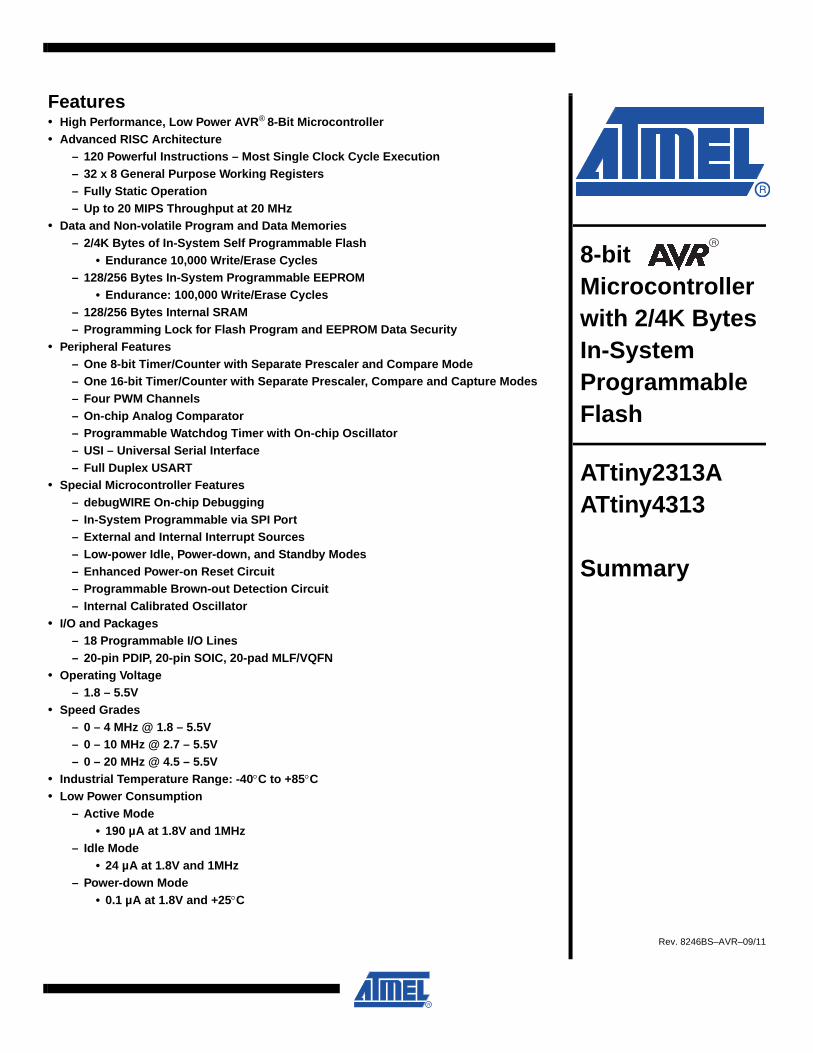
1. Pin Configurations
Figure 1-1. Pinout ATtiny2313A/4313
(PCINT10/RESET/dW) PA2(PCINT11/RXD) PD0(PCINT12/TXD) PD1
(PCINT9/XTAL2) PA1(PCINT8/CLKI/XTAL1) PA0
(PCINT13/CKOUT/XCK/INT0) PD2(PCINT14/INT1) PD3
(PCINT15/T0) PD4(PCINT16/OC0B/T1) PD5
GND
20191817161514131211
12345678910
VCCPB7 (USCK/SCL/SCK/PCINT7)PB6 (MISO/DO/PCINT6)PB5 (MOSI/DI/SDA/PCINT5)PB4 (OC1B/PCINT4)PB3 (OC1A/PCINT3)PB2 (OC0A/PCINT2)PB1 (AIN1/PCINT1)PB0 (AIN0/PCINT0)PD6 (ICPI/PCINT17)
PDIP/SOIC
1
2
3
4
5
MLF/VQFN
15
14
13
12
11
20 19 18 17 16
6 7 8 9 10
(PCINT12/TXD) PD1
(PCINT9/XTAL2) PA1
(PCINT8/CLKI/XTAL1) PA0
(PCINT13/CKOUT/XCK/INT0) PD2
(PCINT14/INT1) PD3
(PC
INT1
5/T0
) PD
4
(PC
INT1
6/O
C0B
/T1)
PD
5
GN
D
(PC
INT1
7/IC
PI)
PD
6
(AIN
0/P
CIN
T0) P
B0
PB5 (MOSI/DI/SDA/PCINT5)
PB4 (OC1B/PCINT4)
PB3 (OC1A/PCINT3)
PB2 (OC0A/PCINT2)
PB1 (AIN1/PCINT1)
PD
0 (R
XD
/PC
INT1
1)
PA2
(RE
SE
T/dW
/PC
INT1
0)
VC
C
PB
7 (U
SC
K/S
CL/
SC
K/P
CIN
T7)
PB
6 (M
ISO
/DO
/PC
INT6
)
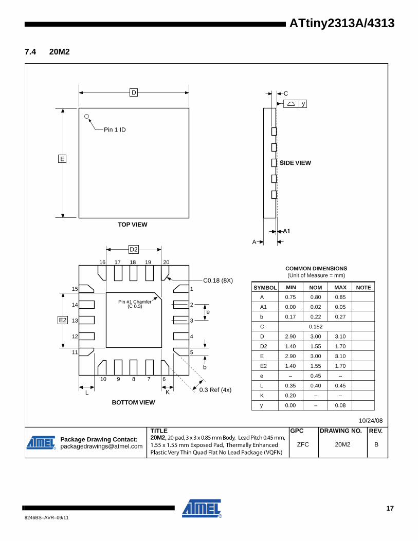
NOTE: Bottom pad should be soldered to ground.
28246BS–AVR–09/11
ATtiny2313A/4313
ATtiny2313A/4313
1.1 Pin Descriptions
1.1.1 VCCDigital supply voltage.
1.1.2 GNDGround.
1.1.3 Port A (PA2..PA0)Port A is a 3-bit bi-directional I/O port with internal pull-up resistors (selected for each bit). ThePort A output buffers have symmetrical drive characteristics with both high sink and sourcecapability, except PA2 which has the RESET capability. To use pin PA2 as I/O pin, instead ofRESET pin, program (“0”) RSTDISBL fuse. As inputs, Port A pins that are externally pulled lowwill source current if the pull-up resistors are activated. The Port A pins are tri-stated when areset condition becomes active, even if the clock is not running.
Port A also serves the functions of various special features of the ATtiny2313A/4313 as listed onpage 61.
1.1.4 Port B (PB7..PB0)Port B is an 8-bit bi-directional I/O port with internal pull-up resistors (selected for each bit). ThePort B output buffers have symmetrical drive characteristics with both high sink and sourcecapability. As inputs, Port B pins that are externally pulled low will source current if the pull-upresistors are activated. The Port B pins are tri-stated when a reset condition becomes active,even if the clock is not running.
Port B also serves the functions of various special features of the ATtiny2313A/4313 as listed onpage 62.
1.1.5 Port D (PD6..PD0)Port D is a 7-bit bi-directional I/O port with internal pull-up resistors (selected for each bit). ThePort D output buffers have symmetrical drive characteristics with both high sink and sourcecapability. As inputs, Port D pins that are externally pulled low will source current if the pull-upresistors are activated. The Port D pins are tri-stated when a reset condition becomes active,even if the clock is not running.
Port D also serves the functions of various special features of the ATtiny2313A/4313 as listed onpage 66.
1.1.6 RESETReset input. A low level on this pin for longer than the minimum pulse length will generate areset, even if the clock is not running and provided that the reset pin has not been disabled. Theminimum pulse length is given in Table 22-3 on page 201. Shorter pulses are not guaranteed togenerate a reset. The Reset Input is an alternate function for PA2 and dW.
The reset pin can also be used as a (weak) I/O pin.
1.1.7 XTAL1Input to the inverting Oscillator amplifier and input to the internal clock operating circuit. XTAL1is an alternate function for PA0.
38246BS–AVR–09/11

1.1.8 XTAL2Output from the inverting Oscillator amplifier. XTAL2 is an alternate function for PA1.
48246BS–AVR–09/11
ATtiny2313A/4313
ATtiny2313A/4313
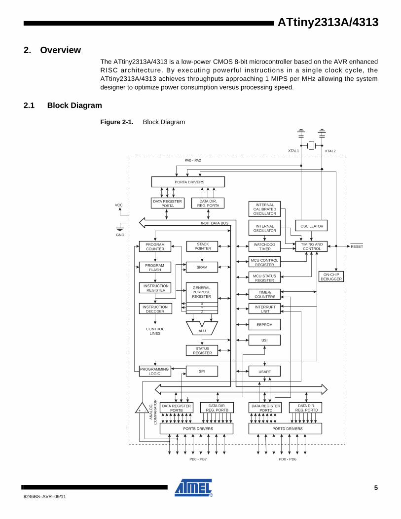
2. OverviewThe ATtiny2313A/4313 is a low-power CMOS 8-bit microcontroller based on the AVR enhancedRISC architecture. By executing powerful instructions in a single clock cycle, theATtiny2313A/4313 achieves throughputs approaching 1 MIPS per MHz allowing the systemdesigner to optimize power consumption versus processing speed.
2.1 Block Diagram
Figure 2-1. Block Diagram
PROGRAMCOUNTER
PROGRAM FLASH
INSTRUCTIONREGISTER
GND
VCC
INSTRUCTIONDECODER
CONTROLLINES
STACKPOINTER
SRAM
GENERALPURPOSEREGISTER
ALU
STATUSREGISTER
PROGRAMMINGLOGIC
SPI
8-BIT DATA BUS
XTAL1 XTAL2
RESET
INTERNALOSCILLATOR
OSCILLATOR
WATCHDOG TIMER
TIMING ANDCONTROL
MCU CONTROLREGISTER
MCU STATUSREGISTER
TIMER/COUNTERS
INTERRUPTUNIT
EEPROM
USI
USART
AN
ALO
GC
OM
PAR
ATO
R
DATA REGISTERPORTB
DATA DIR.REG. PORTB
DATA REGISTERPORTA
DATA DIR.REG. PORTA
PORTB DRIVERS
PB0 - PB7
PORTA DRIVERS
PA0 - PA2
DATA REGISTERPORTD
DATA DIR.REG. PORTD
PORTD DRIVERS
PD0 - PD6
ON-CHIPDEBUGGER
INTERNALCALIBRATEDOSCILLATOR
58246BS–AVR–09/11
The AVR core combines a rich instruction set with 32 general purpose working registers. All the32 registers are directly connected to the Arithmetic Logic Unit (ALU), allowing two independentregisters to be accessed in one single instruction executed in one clock cycle. The resultingarchitecture is more code efficient while achieving throughputs up to ten times faster than con-ventional CISC microcontrollers.
The ATtiny2313A/4313 provides the following features: 2/4K bytes of In-System ProgrammableFlash, 128/256 bytes EEPROM, 128/256 bytes SRAM, 18 general purpose I/O lines, 32 generalpurpose working registers, a single-wire Interface for On-chip Debugging, two flexibleTimer/Counters with compare modes, internal and external interrupts, a serial programmableUSART, Universal Serial Interface with Start Condition Detector, a programmable WatchdogTimer with internal Oscillator, and three software selectable power saving modes. The Idle modestops the CPU while allowing the SRAM, Timer/Counters, and interrupt system to continue func-tioning. The Power-down mode saves the register contents but freezes the Oscillator, disablingall other chip functions until the next interrupt or hardware reset. In Standby mode, the crys-tal/resonator Oscillator is running while the rest of the device is sleeping. This allows very faststart-up combined with low-power consumption.
The device is manufactured using Atmel’s high density non-volatile memory technology. TheOn-chip ISP Flash allows the program memory to be reprogrammed In-System through an SPIserial interface, or by a conventional non-volatile memory programmer. By combining an 8-bitRISC CPU with In-System Self-Programmable Flash on a monolithic chip, the AtmelATtiny2313A/4313 is a powerful microcontroller that provides a highly flexible and cost effectivesolution to many embedded control applications.
The ATtiny2313A/4313 AVR is supported with a full suite of program and system developmenttools including: C Compilers, Macro Assemblers, Program Debugger/Simulators, In-Circuit Emu-lators, and Evaluation kits.
2.2 Comparison Between ATtiny2313A and ATtiny4313The ATtiny2313A and ATtiny4313 differ only in memory sizes. Table 2-1 summarizes the differ-ent memory sizes for the two devices.
Table 2-1. Memory Size Summary
Device Flash EEPROM RAM
ATtiny2313A 2K Bytes 128 Bytes 128 Bytes
ATtiny4313 4K Bytes 256 Bytes 256 Bytes
68246BS–AVR–09/11
ATtiny2313A/4313
ATtiny2313A/4313
3. About
3.1 ResourcesA comprehensive set of drivers, application notes, data sheets and descriptions on developmenttools are available for download at http://www.atmel.com/avr.
3.2 Code ExamplesThis documentation contains simple code examples that briefly show how to use various parts ofthe device. These code examples assume that the part specific header file is included beforecompilation. Be aware that not all C compiler vendors include bit definitions in the header filesand interrupt handling in C is compiler dependent. Please confirm with the C compiler documen-tation for more details.
For I/O Registers located in the extended I/O map, “IN”, “OUT”, “SBIS”, “SBIC”, “CBI”, and “SBI”instructions must be replaced with instructions that allow access to extended I/O. Typically, thismeans “LDS” and “STS” combined with “SBRS”, “SBRC”, “SBR”, and “CBR”. Note that not allAVR devices include an extended I/O map.
3.3 Data RetentionReliability Qualification results show that the projected data retention failure rate is much lessthan 1 PPM over 20 years at 85°C or 100 years at 25°C.
78246BS–AVR–09/11
4. Register SummaryAddress Name Bit 7 Bit 6 Bit 5 Bit 4 Bit 3 Bit 2 Bit 1 Bit 0 Page
0x3F (0x5F) SREG I T H S V N Z C 9
0x3E (0x5E) Reserved – – – – – – – –
0x3D (0x5D) SPL SP7 SP6 SP5 SP4 SP3 SP2 SP1 SP0 12
0x3C (0x5C) OCR0B Timer/Counter0 – Compare Register B 85
0x3B (0x5B) GIMSK INT1 INT0 PCIE0 PCIE2 PCIE1 – – – 50
0x3A (0x5A) GIFR INTF1 INTF0 PCIF0 PCIF2 PCIF1 – – – 51
0x39 (0x59) TIMSK TOIE1 OCIE1A OCIE1B – ICIE1 OCIE0B TOIE0 OCIE0A 86, 115
0x38 (0x58) TIFR TOV1 OCF1A OCF1B – ICF1 OCF0B TOV0 OCF0A 86, 115
0x37 (0x57) SPMCSR – – RSIG CTPB RFLB PGWRT PGERS SPMEN 175
0x36 (0x56) OCR0A Timer/Counter0 – Compare Register A 85
0x35 (0x55) MCUCR PUD SM1 SE SM0 ISC11 ISC10 ISC01 ISC00 36, 50, 68
0x34 (0x54) MCUSR – – – – WDRF BORF EXTRF PORF 44
0x33 (0x53) TCCR0B FOC0A FOC0B – – WGM02 CS02 CS01 CS00 84
0x32 (0x52) TCNT0 Timer/Counter0 (8-bit) 85
0x31 (0x51) OSCCAL – CAL6 CAL5 CAL4 CAL3 CAL2 CAL1 CAL0 31
0x30 (0x50) TCCR0A COM0A1 COM0A0 COM0B1 COM0B0 – – WGM01 WGM00 81
0x2F (0x4F) TCCR1A COM1A1 COM1A0 COM1B1 COM1B0 – – WGM11 WGM10 110
0x2E (0x4E) TCCR1B ICNC1 ICES1 – WGM13 WGM12 CS12 CS11 CS10 112
0x2D (0x4D) TCNT1H Timer/Counter1 – Counter Register High Byte 114
0x2C (0x4C) TCNT1L Timer/Counter1 – Counter Register Low Byte 114
0x2B (0x4B) OCR1AH Timer/Counter1 – Compare Register A High Byte 114
0x2A (0x4A) OCR1AL Timer/Counter1 – Compare Register A Low Byte 114
0x29 (0x49) OCR1BH Timer/Counter1 – Compare Register B High Byte 114
0x28 (0x48) OCR1BL Timer/Counter1 – Compare Register B Low Byte 114
0x27 (0x47) Reserved – – – – – – – –
0x26 (0x46) CLKPR CLKPCE – – – CLKPS3 CLKPS2 CLKPS1 CLKPS0 31
0x25 (0x45) ICR1H Timer/Counter1 - Input Capture Register High Byte 114
0x24 (0x44) ICR1L Timer/Counter1 - Input Capture Register Low Byte 114
0x23 (0x43) GTCCR – – – – – – – PSR10 118
0x22 (ox42) TCCR1C FOC1A FOC1B – – – – – – 113
0x21 (0x41) WDTCSR WDIF WDIE WDP3 WDCE WDE WDP2 WDP1 WDP0 44
0x20 (0x40) PCMSK0 PCINT7 PCINT6 PCINT5 PCINT4 PCINT3 PCINT2 PCINT1 PCINT0 53
0x1F (0x3F) Reserved – – – – – – – –
0x1E (0x3E) EEAR – EEPROM Address Register 23
0x1D (0x3D) EEDR EEPROM Data Register 23
0x1C (0x3C) EECR – – EEPM1 EEPM0 EERIE EEMPE EEPE EERE 23
0x1B (0x3B) PORTA – – – – – PORTA2 PORTA1 PORTA0 68
0x1A (0x3A) DDRA – – – – – DDA2 DDA1 DDA0 68
0x19 (0x39) PINA – – – – – PINA2 PINA1 PINA0 69
0x18 (0x38) PORTB PORTB7 PORTB6 PORTB5 PORTB4 PORTB3 PORTB2 PORTB1 PORTB0 69
0x17 (0x37) DDRB DDB7 DDB6 DDB5 DDB4 DDB3 DDB2 DDB1 DDB0 69
0x16 (0x36) PINB PINB7 PINB6 PINB5 PINB4 PINB3 PINB2 PINB1 PINB0 69
0x15 (0x35) GPIOR2 General Purpose I/O Register 2 24
0x14 (0x34) GPIOR1 General Purpose I/O Register 1 24
0x13 (0x33) GPIOR0 General Purpose I/O Register 0 24
0x12 (0x32) PORTD – PORTD6 PORTD5 PORTD4 PORTD3 PORTD2 PORTD1 PORTD0 69
0x11 (0x31) DDRD – DDD6 DDD5 DDD4 DDD3 DDD2 DDD1 DDD0 69
0x10 (0x30) PIND – PIND6 PIND5 PIND4 PIND3 PIND2 PIND1 PIND0 69
0x0F (0x2F) USIDR USI Data Register 165
0x0E (0x2E) USISR USISIF USIOIF USIPF USIDC USICNT3 USICNT2 USICNT1 USICNT0 164
0x0D (0x2D) USICR USISIE USIOIE USIWM1 USIWM0 USICS1 USICS0 USICLK USITC 162
0x0C (0x2C) UDR UART Data Register (8-bit) 136
0x0B (0x2B) UCSRA RXC TXC UDRE FE DOR UPE U2X MPCM 137
0x0A (0x2A) UCSRB RXCIE TXCIE UDRIE RXEN TXEN UCSZ2 RXB8 TXB8 138
0x09 (0x29) UBRRL UBRRH[7:0] 140
0x08 (0x28) ACSR ACD ACBG ACO ACI ACIE ACIC ACIS1 ACIS0 167
0x07 (0x27) BODCR – – – – – – BODS BODSE 37
0x06 (0x26) PRR – – – – PRTIM1 PRTIM0 PRUSI PRUSART 36
0x05 (0x25) PCMSK2 – PCINT17 PCINT16 PCINT15 PCINT14 PCINT13 PCINT12 PCINT11 52
0x04 (0x24) PCMSK1 – – – – – PCINT10 PCINT9 PCINT8 52
0x03 (0x23) UCSRC UMSEL1 UMSEL0 UPM1 UPM0 USBS UCSZ1 UCSZ0 UCPOL 139
0x02 (0x22) UBRRH – – – – UBRRH[11:8] 140
0x01 (0x21) DIDR – – – – – – AIN1D AIN0D 168
0x00 (0x20) USIBR USI Buffer Register 166
88246BS–AVR–09/11
ATtiny2313A/4313
ATtiny2313A/4313
Notes: 1. For compatibility with future devices, reserved bits should be written to zero if accessed. Reserved I/O memory addresses should never be written.
2. I/O Registers within the address range 0x00 - 0x1F are directly bit-accessible using the SBI and CBI instructions. In these registers, the value of single bits can be checked by using the SBIS and SBIC instructions.
3. Some of the status flags are cleared by writing a logical one to them. Note that, unlike most other AVRs, the CBI and SBI instructions will only operate on the specified bit, and can therefore be used on registers containing such status flags. The CBI and SBI instructions work with registers 0x00 to 0x1F only.
4. When using the I/O specific commands IN and OUT, the I/O addresses 0x00 - 0x3F must be used. When addressing I/O Registers as data space using LD and ST instructions, 0x20 must be added to these addresses.
98246BS–AVR–09/11
5. Instruction Set SummaryMnemonics Operands Description Operation Flags #Clocks
ARITHMETIC AND LOGIC INSTRUCTIONS
ADD Rd, Rr Add two Registers Rd ← Rd + Rr Z,C,N,V,H 1
ADC Rd, Rr Add with Carry two Registers Rd ← Rd + Rr + C Z,C,N,V,H 1
ADIW Rdl,K Add Immediate to Word Rdh:Rdl ← Rdh:Rdl + K Z,C,N,V,S 2
SUB Rd, Rr Subtract two Registers Rd ← Rd - Rr Z,C,N,V,H 1
SUBI Rd, K Subtract Constant from Register Rd ← Rd - K Z,C,N,V,H 1
SBC Rd, Rr Subtract with Carry two Registers Rd ← Rd - Rr - C Z,C,N,V,H 1
SBCI Rd, K Subtract with Carry Constant from Reg. Rd ← Rd - K - C Z,C,N,V,H 1
SBIW Rdl,K Subtract Immediate from Word Rdh:Rdl ← Rdh:Rdl - K Z,C,N,V,S 2
AND Rd, Rr Logical AND Registers Rd ← Rd • Rr Z,N,V 1
ANDI Rd, K Logical AND Register and Constant Rd ← Rd • K Z,N,V 1
OR Rd, Rr Logical OR Registers Rd ← Rd v Rr Z,N,V 1
ORI Rd, K Logical OR Register and Constant Rd ← Rd v K Z,N,V 1
EOR Rd, Rr Exclusive OR Registers Rd ← Rd ⊕ Rr Z,N,V 1
COM Rd One’s Complement Rd ← 0xFF − Rd Z,C,N,V 1
NEG Rd Two’s Complement Rd ← 0x00 − Rd Z,C,N,V,H 1
SBR Rd,K Set Bit(s) in Register Rd ← Rd v K Z,N,V 1
CBR Rd,K Clear Bit(s) in Register Rd ← Rd • (0xFF - K) Z,N,V 1
INC Rd Increment Rd ← Rd + 1 Z,N,V 1
DEC Rd Decrement Rd ← Rd − 1 Z,N,V 1
TST Rd Test for Zero or Minus Rd ← Rd • Rd Z,N,V 1
CLR Rd Clear Register Rd ← Rd ⊕ Rd Z,N,V 1
SER Rd Set Register Rd ← 0xFF None 1
BRANCH INSTRUCTIONS
RJMP k Relative Jump PC ← PC + k + 1 None 2
IJMP Indirect Jump to (Z) PC ← Z None 2
RCALL k Relative Subroutine Call PC ← PC + k + 1 None 3
ICALL Indirect Call to (Z) PC ← Z None 3
RET Subroutine Return PC ← STACK None 4
RETI Interrupt Return PC ← STACK I 4
CPSE Rd,Rr Compare, Skip if Equal if (Rd = Rr) PC ← PC + 2 or 3 None 1/2/3
CP Rd,Rr Compare Rd − Rr Z, N,V,C,H 1
CPC Rd,Rr Compare with Carry Rd − Rr − C Z, N,V,C,H 1
CPI Rd,K Compare Register with Immediate Rd − K Z, N,V,C,H 1
SBRC Rr, b Skip if Bit in Register Cleared if (Rr(b)=0) PC ← PC + 2 or 3 None 1/2/3
SBRS Rr, b Skip if Bit in Register is Set if (Rr(b)=1) PC ← PC + 2 or 3 None 1/2/3
SBIC P, b Skip if Bit in I/O Register Cleared if (P(b)=0) PC ← PC + 2 or 3 None 1/2/3
SBIS P, b Skip if Bit in I/O Register is Set if (P(b)=1) PC ← PC + 2 or 3 None 1/2/3
BRBS s, k Branch if Status Flag Set if (SREG(s) = 1) then PC←PC+k + 1 None 1/2
BRBC s, k Branch if Status Flag Cleared if (SREG(s) = 0) then PC←PC+k + 1 None 1/2
BREQ k Branch if Equal if (Z = 1) then PC ← PC + k + 1 None 1/2
BRNE k Branch if Not Equal if (Z = 0) then PC ← PC + k + 1 None 1/2
BRCS k Branch if Carry Set if (C = 1) then PC ← PC + k + 1 None 1/2
BRCC k Branch if Carry Cleared if (C = 0) then PC ← PC + k + 1 None 1/2
BRSH k Branch if Same or Higher if (C = 0) then PC ← PC + k + 1 None 1/2
BRLO k Branch if Lower if (C = 1) then PC ← PC + k + 1 None 1/2
BRMI k Branch if Minus if (N = 1) then PC ← PC + k + 1 None 1/2
BRPL k Branch if Plus if (N = 0) then PC ← PC + k + 1 None 1/2
BRGE k Branch if Greater or Equal, Signed if (N ⊕ V= 0) then PC ← PC + k + 1 None 1/2
BRLT k Branch if Less Than Zero, Signed if (N ⊕ V= 1) then PC ← PC + k + 1 None 1/2
BRHS k Branch if Half Carry Flag Set if (H = 1) then PC ← PC + k + 1 None 1/2
BRHC k Branch if Half Carry Flag Cleared if (H = 0) then PC ← PC + k + 1 None 1/2
BRTS k Branch if T Flag Set if (T = 1) then PC ← PC + k + 1 None 1/2
BRTC k Branch if T Flag Cleared if (T = 0) then PC ← PC + k + 1 None 1/2
BRVS k Branch if Overflow Flag is Set if (V = 1) then PC ← PC + k + 1 None 1/2
BRVC k Branch if Overflow Flag is Cleared if (V = 0) then PC ← PC + k + 1 None 1/2
BRIE k Branch if Interrupt Enabled if ( I = 1) then PC ← PC + k + 1 None 1/2
BRID k Branch if Interrupt Disabled if ( I = 0) then PC ← PC + k + 1 None 1/2
BIT AND BIT-TEST INSTRUCTIONS
SBI P,b Set Bit in I/O Register I/O(P,b) ← 1 None 2
CBI P,b Clear Bit in I/O Register I/O(P,b) ← 0 None 2
LSL Rd Logical Shift Left Rd(n+1) ← Rd(n), Rd(0) ← 0 Z,C,N,V 1
LSR Rd Logical Shift Right Rd(n) ← Rd(n+1), Rd(7) ← 0 Z,C,N,V 1
ROL Rd Rotate Left Through Carry Rd(0)←C,Rd(n+1)← Rd(n),C←Rd(7) Z,C,N,V 1
108246BS–AVR–09/11
ATtiny2313A/4313
ATtiny2313A/4313
ROR Rd Rotate Right Through Carry Rd(7)←C,Rd(n)← Rd(n+1),C←Rd(0) Z,C,N,V 1
ASR Rd Arithmetic Shift Right Rd(n) ← Rd(n+1), n=0..6 Z,C,N,V 1
SWAP Rd Swap Nibbles Rd(3..0)←Rd(7..4),Rd(7..4)←Rd(3..0) None 1
BSET s Flag Set SREG(s) ← 1 SREG(s) 1
BCLR s Flag Clear SREG(s) ← 0 SREG(s) 1
BST Rr, b Bit Store from Register to T T ← Rr(b) T 1
BLD Rd, b Bit load from T to Register Rd(b) ← T None 1
SEC Set Carry C ← 1 C 1
CLC Clear Carry C ← 0 C 1
SEN Set Negative Flag N ← 1 N 1
CLN Clear Negative Flag N ← 0 N 1
SEZ Set Zero Flag Z ← 1 Z 1
CLZ Clear Zero Flag Z ← 0 Z 1
SEI Global Interrupt Enable I ← 1 I 1
CLI Global Interrupt Disable I ← 0 I 1
SES Set Signed Test Flag S ← 1 S 1
CLS Clear Signed Test Flag S ← 0 S 1
SEV Set Twos Complement Overflow. V ← 1 V 1
CLV Clear Twos Complement Overflow V ← 0 V 1
SET Set T in SREG T ← 1 T 1
CLT Clear T in SREG T ← 0 T 1
SEH Set Half Carry Flag in SREG H ← 1 H 1
CLH Clear Half Carry Flag in SREG H ← 0 H 1
DATA TRANSFER INSTRUCTIONS
MOV Rd, Rr Move Between Registers Rd ← Rr None 1
MOVW Rd, Rr Copy Register Word Rd+1:Rd ← Rr+1:Rr None 1
LDI Rd, K Load Immediate Rd ← K None 1
LD Rd, X Load Indirect Rd ← (X) None 2
LD Rd, X+ Load Indirect and Post-Inc. Rd ← (X), X ← X + 1 None 2
LD Rd, - X Load Indirect and Pre-Dec. X ← X - 1, Rd ← (X) None 2
LD Rd, Y Load Indirect Rd ← (Y) None 2
LD Rd, Y+ Load Indirect and Post-Inc. Rd ← (Y), Y ← Y + 1 None 2
LD Rd, - Y Load Indirect and Pre-Dec. Y ← Y - 1, Rd ← (Y) None 2
LDD Rd,Y+q Load Indirect with Displacement Rd ← (Y + q) None 2
LD Rd, Z Load Indirect Rd ← (Z) None 2
LD Rd, Z+ Load Indirect and Post-Inc. Rd ← (Z), Z ← Z+1 None 2
LD Rd, -Z Load Indirect and Pre-Dec. Z ← Z - 1, Rd ← (Z) None 2
LDD Rd, Z+q Load Indirect with Displacement Rd ← (Z + q) None 2
LDS Rd, k Load Direct from SRAM Rd ← (k) None 2
ST X, Rr Store Indirect (X) ← Rr None 2
ST X+, Rr Store Indirect and Post-Inc. (X) ← Rr, X ← X + 1 None 2
ST - X, Rr Store Indirect and Pre-Dec. X ← X - 1, (X) ← Rr None 2
ST Y, Rr Store Indirect (Y) ← Rr None 2
ST Y+, Rr Store Indirect and Post-Inc. (Y) ← Rr, Y ← Y + 1 None 2
ST - Y, Rr Store Indirect and Pre-Dec. Y ← Y - 1, (Y) ← Rr None 2
STD Y+q,Rr Store Indirect with Displacement (Y + q) ← Rr None 2
ST Z, Rr Store Indirect (Z) ← Rr None 2
ST Z+, Rr Store Indirect and Post-Inc. (Z) ← Rr, Z ← Z + 1 None 2
ST -Z, Rr Store Indirect and Pre-Dec. Z ← Z - 1, (Z) ← Rr None 2
STD Z+q,Rr Store Indirect with Displacement (Z + q) ← Rr None 2
STS k, Rr Store Direct to SRAM (k) ← Rr None 2
LPM Load Program Memory R0 ← (Z) None 3
LPM Rd, Z Load Program Memory Rd ← (Z) None 3
LPM Rd, Z+ Load Program Memory and Post-Inc Rd ← (Z), Z ← Z+1 None 3
SPM Store Program Memory (Z) ← R1:R0 None -
IN Rd, P In Port Rd ← P None 1
OUT P, Rr Out Port P ← Rr None 1
PUSH Rr Push Register on Stack STACK ← Rr None 2
POP Rd Pop Register from Stack Rd ← STACK None 2
MCU CONTROL INSTRUCTIONS
NOP No Operation None 1
SLEEP Sleep (see specific descr. for Sleep function) None 1
WDR Watchdog Reset (see specific descr. for WDR/timer) None 1
BREAK Break For On-chip Debug Only None N/A
Mnemonics Operands Description Operation Flags #Clocks
118246BS–AVR–09/11
6. Ordering Information
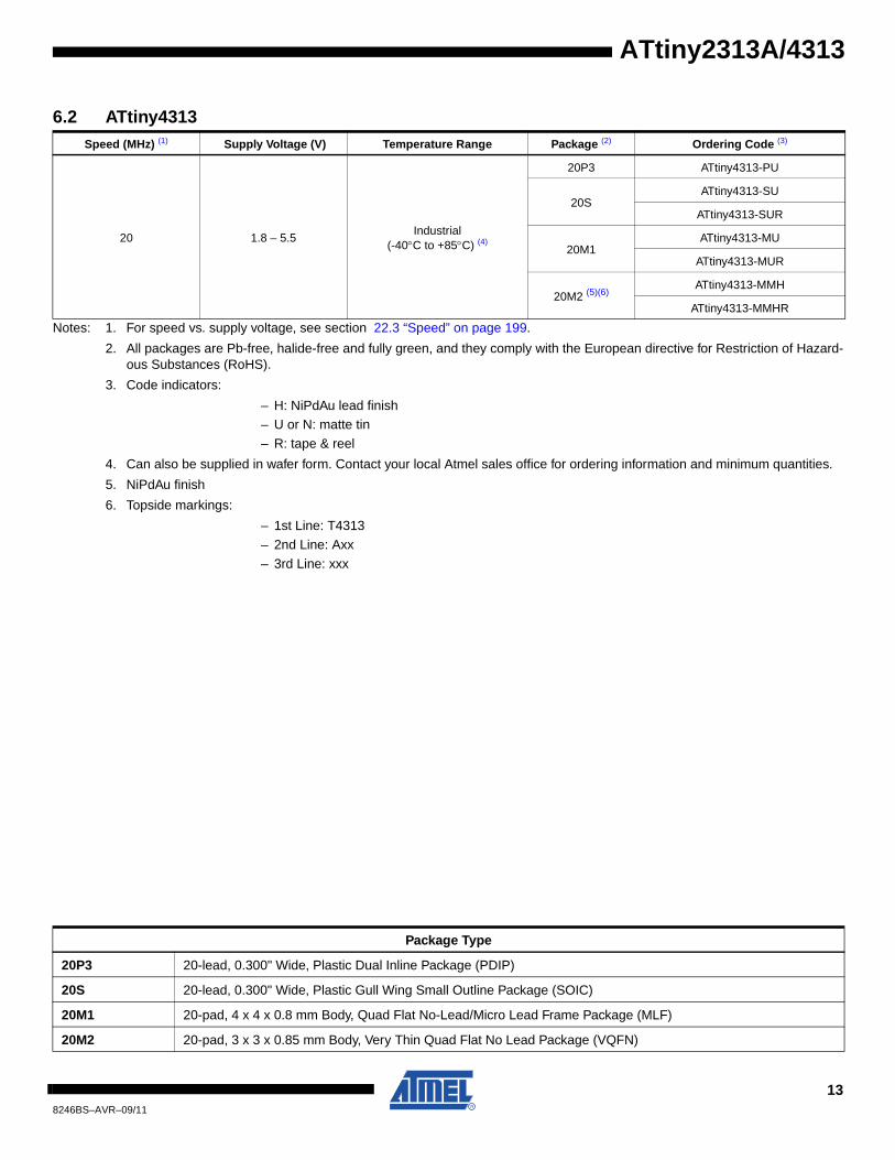
Notes: 1. For speed vs. supply voltage, see section 22.3 “Speed” on page 199.
2. All packages are Pb-free, halide-free and fully green, and they comply with the European directive for Restriction of Hazard-ous Substances (RoHS).
3. Code indicators:
– H: NiPdAu lead finish
– U or N: matte tin– R: tape & reel
4. Can also be supplied in wafer form. Contact your local Atmel sales office for ordering information and minimum quantities.
5. NiPdAu finish
6. Topside markings :
– 1st Line: T2313– 2nd Line: Axx
– 3rd Line: xxx
6.1 ATtiny2313ASpeed (MHz) (1) Supply Voltage (V) Temperature Range Package (2) Ordering Code (3)
20 1.8 – 5.5Industrial
(-40°C to +85°C) (4)
20P3 ATtiny2313A-PU
20SATtiny2313A-SU
ATtiny2313A-SUR
20M1ATtiny2313A-MU
ATtiny2313A-MUR
20M2 (5)(6)ATtiny2313A-MMH
ATtiny2313A-MMHR
Package Type
20P3 20-lead, 0.300" Wide, Plastic Dual Inline Package (PDIP)
20S 20-lead, 0.300" Wide, Plastic Gull Wing Small Outline Package (SOIC)
20M1 20-pad, 4 x 4 x 0.8 mm Body, Quad Flat No-Lead / Micro Lead Frame Package (MLF)
20M2 20-pad, 3 x 3 x 0.85 mm Body, Very Thin Quad Flat No Lead Package (VQFN)
128246BS–AVR–09/11
ATtiny2313A/4313
ATtiny2313A/4313
Notes: 1. For speed vs. supply voltage, see section 22.3 “Speed” on page 199.
2. All packages are Pb-free, halide-free and fully green, and they comply with the European directive for Restriction of Hazard-ous Substances (RoHS).
3. Code indicators:
– H: NiPdAu lead finish– U or N: matte tin
– R: tape & reel
4. Can also be supplied in wafer form. Contact your local Atmel sales office for ordering information and minimum quantities.
5. NiPdAu finish
6. Topside markings:
– 1st Line: T4313
– 2nd Line: Axx
– 3rd Line: xxx
6.2 ATtiny4313Speed (MHz) (1) Supply Voltage (V) Temperature Range Package (2) Ordering Code (3)
20 1.8 – 5.5Industrial
(-40°C to +85°C) (4)
20P3 ATtiny4313-PU
20SATtiny4313-SU
ATtiny4313-SUR
20M1ATtiny4313-MU
ATtiny4313-MUR
20M2 (5)(6)ATtiny4313-MMH
ATtiny4313-MMHR
Package Type
20P3 20-lead, 0.300" Wide, Plastic Dual Inline Package (PDIP)
20S 20-lead, 0.300" Wide, Plastic Gull Wing Small Outline Package (SOIC)
20M1 20-pad, 4 x 4 x 0.8 mm Body, Quad Flat No-Lead/Micro Lead Frame Package (MLF)
20M2 20-pad, 3 x 3 x 0.85 mm Body, Very Thin Quad Flat No Lead Package (VQFN)
138246BS–AVR–09/11
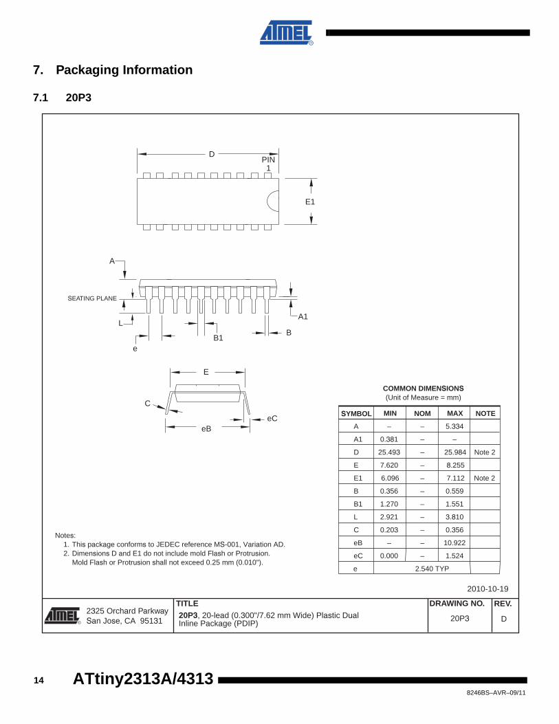
7. Packaging Information
7.1 20P3
2325 Orchard Parkway San Jose, CA 95131
TITLE DRAWING NO.
R
REV. 20P3, 20-lead (0.300"/7.62 mm Wide) Plastic Dual Inline Package (PDIP) D20P3
2010-10-19
PIN1
E1
A1
B
E
B1
C
L
SEATING PLANE
A
D
e
eBeC
COMMON DIMENSIONS(Unit of Measure = mm)
SYMBOL MIN NOM MAX NOTE
A – – 5.334
A1 0.381 – –
D 25.493 – 25.984 Note 2
E 7.620 – 8.255
E1 6.096 – 7.112 Note 2
B 0.356 – 0.559
B1 1.270 – 1.551
L 2.921 – 3.810
C 0.203 – 0.356
eB – – 10.922
eC 0.000 – 1.524
e 2.540 TYP
Notes: 1. This package conforms to JEDEC reference MS-001, Variation AD. 2. Dimensions D and E1 do not include mold Flash or Protrusion. Mold Flash or Protrusion shall not exceed 0.25 mm (0.010").
148246BS–AVR–09/11
ATtiny2313A/4313
ATtiny2313A/4313
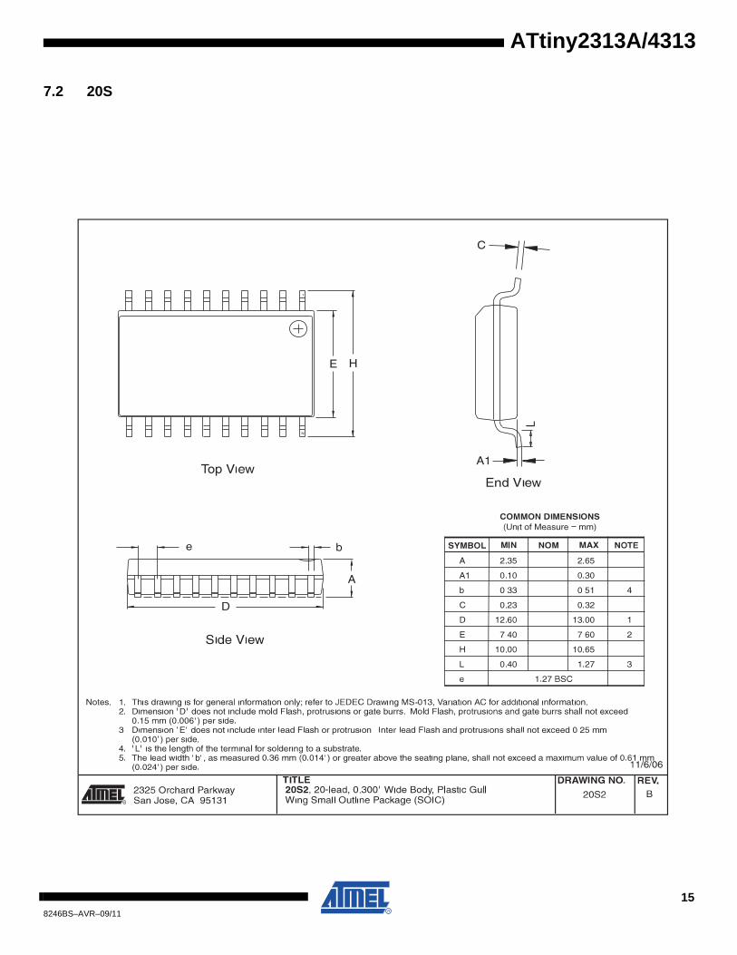
7.2 20S
158246BS–AVR–09/11
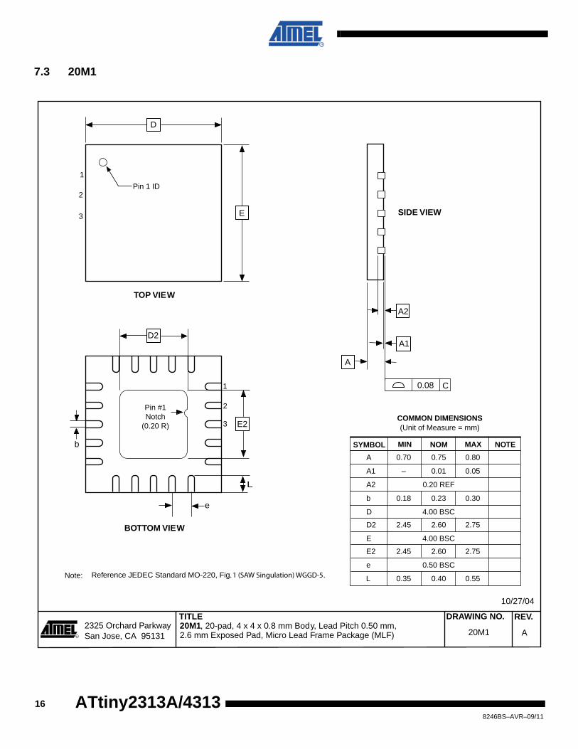
7.3 20M1
2325 Orchard Parkway San Jose, CA 95131
TITLE DRAWING NO.
R
REV. 20M1, 20-pad, 4 x 4 x 0.8 mm Body, Lead Pitch 0.50 mm,
A20M1
10/27/04
2.6 mm Exposed Pad, Micro Lead Frame Package (MLF)
A 0.70 0.75 0.80
A1 – 0.01 0.05
A2 0.20 REF
b 0.18 0.23 0.30
D 4.00 BSC
D2 2.45 2.60 2.75
E 4.00 BSC
E2 2.45 2.60 2.75
e 0.50 BSC
L 0.35 0.40 0.55
SIDE VIEW
Pin 1 ID
Pin #1 Notch
(0.20 R)
BOTTOM VIEW
TOP VIEW
Note: Reference JEDEC Standard MO-220, Fig. 1 (SAW Singulation) WGGD-5.
COMMON DIMENSIONS(Unit of Measure = mm)
SYMBOL MIN NOM MAX NOTE
D
E
e
A2
A1
A
D2
E2
0.08 C
L
1
2
3
b
1
2
3
168246BS–AVR–09/11
ATtiny2313A/4313
ATtiny2313A/4313
7.4 20M2
TITLE DRAWING NO. GPC REV. Package Drawing Contact: [email protected] 20M2 ZFC B
20M2, 20-pad, 3 x 3 x 0.85 mm Body, Lead Pitch 0.45 mm, 1.55 x 1.55 mm Exposed Pad, Thermally Enhanced Plastic Very Thin Quad Flat No Lead Package (VQFN)
10/24/08
15
14
13
12
11
1
2
3
4
5
16 17 18 19 20
10 9 8 7 6
D2
E2 e
b
K L
Pin #1 Chamfer (C 0.3)
D
E SIDE VIEW
A1
y
Pin 1 ID
BOTTOM VIEW
TOP VIEW A1
A
C
C0.18 (8X)
0.3 Ref (4x)
COMMON DIMENSIONS (Unit of Measure = mm)
SYMBOL MIN NOM MAX NOTE
A 0.75 0.80 0.85
A1 0.00 0.02 0.05
b 0.17 0.22 0.27
C 0.152
D 2.90 3.00 3.10
D2 1.40 1.55 1.70
E 2.90 3.00 3.10
E2 1.40 1.55 1.70
e – 0.45 –
L 0.35 0.40 0.45
K 0.20 – –
y 0.00 – 0.08
178246BS–AVR–09/11
8. ErrataThe revision letters in this section refer to the revision of the corresponding ATtiny2313A/4313device.
8.1 ATtiny2313A
8.1.1 Rev. DNo known errata.
8.1.2 Rev. A – CThese device revisions were referred to as ATtiny2313/ATtiny2313V.
8.2 ATtiny4313
8.2.1 Rev. ANo known errata.
188246BS–AVR–09/11
ATtiny2313A/4313
ATtiny2313A/4313
9. Datasheet Revision History
9.1 Rev. 8246B – 10/111. Updated device status from Preliminary to Final.
2. Updated document template.
3. Added order codes for tape&reel devices, on page 259 and page 260
4. Updated figures:
– Figure 23-33 on page 223
– Figure 23-44 on page 228
– Figure 23-81 on page 247
– Figure 23-92 on page 252
5. Updated sections:
– Section 5. “Memories” on page 15
– Section 19. “Self-Programming” on page 172
– Section 20. “Lock Bits, Fuse Bits and Device Signature” on page 177
– Section 21. “External Programming” on page 183
– Section 26. “Ordering Information” on page 259
9.2 Rev. 8246A – 11/091. Initial revision. Created from document 2543_t2313.
2. Updated datasheet template.
3. Added VQFN in the Pinout Figure 1-1 on page 2.
4. Added Section 7.2 “Software BOD Disable” on page 34.
5. Added Section 7.3 “Power Reduction Register” on page 34.
6. Updated Table 7-2, “Sleep Mode Select,” on page 36.
7. Added Section 7.5.3 “BODCR – Brown-Out Detector Control Register” on page 37.
8. Added reset disable function in Figure 8-1 on page 38.
9. Added pin change interrupts PCINT1 and PCINT2 in Table 9-1 on page 47.
10. Added PCINT17..8 and PCMSK2..1 in Section 9.2 “External Interrupts” on page 48.
11. Added Section 9.3.4 “PCMSK2 – Pin Change Mask Register 2” on page 52.
12. Added Section 9.3.5 “PCMSK1 – Pin Change Mask Register 1” on page 52.
13. Updated Section 10.2.1 “Alternate Functions of Port A” on page 61.
14. Updated Section 10.2.2 “Alternate Functions of Port B” on page 62.
15. Updated Section 10.2.3 “Alternate Functions of Port D” on page 66.
16. Added UMSEL1 and UMSEL0 in Section 14.10.4 “UCSRC – USART Control and Sta-tus Register C” on page 139.
17. Added Section 15. “USART in SPI Mode” on page 145.
18. Added USI Buffer Register (USIBR) in Section 16.2 “Overview” on page 155 and in Fig-ure 16-1 on page 155.
19. Added Section 16.5.4 “USIBR – USI Buffer Register” on page 166.
20. Updated Section 19.6.3 “Reading Device Signature Imprint Table from Firmware” on page 175.
198246BS–AVR–09/11
21. Updated Section 19.7.1 “SPMCSR – Store Program Memory Control and Status Regis-ter” on page 175.
22. Added Section 20.3 “Device Signature Imprint Table” on page 179.
23. Updated Section 20.3.1 “Calibration Byte” on page 180.
24. Changed BS to BS1 in Section 20.6.13 “Reading the Signature Bytes” on page 189.
25. Updated Section 22.2 “DC Characteristics” on page 198.
26. Added Section 23.1 “Effect of Power Reduction” on page 206.
27. Updated characteristic plots in Section 23. “Typical Characteristics” for ATtiny2313A (pages 207 - 230), and added plots for ATtiny4313 (pages 231 - 254).
28. Updated Section 24. “Register Summary” on page 255 .
29. Updated Section 26. “Ordering Information” on page 259, added the package type 20M2 and the ordering code -MMH (VQFN), and added the topside marking note.
208246BS–AVR–09/11
ATtiny2313A/4313

ATtiny2313A/4313
218246BS–AVR–09/11
8246BS–AVR–09/11
Headquarters International
Atmel Corporation2325 Orchard ParkwaySan Jose, CA 95131USATel: 1(408) 441-0311Fax: 1(408) 487-2600
Atmel Asia LimitedUnit 01-5 & 16, 19/FBEA Tower, Millennium City 5418 Kwun Tong RoadKwun Tong, KowloonHONG KONGTel: (852) 2245-6100Fax: (852) 2722-1369
Atmel Munich GmbHBusiness CampusParkring 4D-85748 Garching b. MunichGERMANYTel: (+49) 89-31970-0Fax: (+49) 89-3194621
Atmel Japan9F, Tonetsu Shinkawa Bldg.1-24-8 ShinkawaChuo-ku, Tokyo 104-0033JAPANTel: (81) 3-3523-3551Fax: (81) 3-3523-7581
Product Contact
Web Sitewww.atmel.com
Technical [email protected]
Sales Contactwww.atmel.com/contacts
Literature Requestswww.atmel.com/literature
Disclaimer: The information in this document is provided in connection with Atmel products. No license, express or implied, by estoppel or otherwise, to anyintellectual property right is granted by this document or in connection with the sale of Atmel products. EXCEPT AS SET FORTH IN ATMEL’S TERMS AND CONDI-TIONS OF SALE LOCATED ON ATMEL’S WEB SITE, ATMEL ASSUMES NO LIABILITY WHATSOEVER AND DISCLAIMS ANY EXPRESS, IMPLIED OR STATUTORYWARRANTY RELATING TO ITS PRODUCTS INCLUDING, BUT NOT LIMITED TO, THE IMPLIED WARRANTY OF MERCHANTABILITY, FITNESS FOR A PARTICULARPURPOSE, OR NON-INFRINGEMENT. IN NO EVENT SHALL ATMEL BE LIABLE FOR ANY DIRECT, INDIRECT, CONSEQUENTIAL, PUNITIVE, SPECIAL OR INCIDEN-TAL DAMAGES (INCLUDING, WITHOUT LIMITATION, DAMAGES FOR LOSS OF PROFITS, BUSINESS INTERRUPTION, OR LOSS OF INFORMATION) ARISING OUT OFTHE USE OR INABILITY TO USE THIS DOCUMENT, EVEN IF ATMEL HAS BEEN ADVISED OF THE POSSIBILITY OF SUCH DAMAGES. Atmel makes norepresentations or warranties with respect to the accuracy or completeness of the contents of this document and reserves the right to make changes to specificationsand product descriptions at any time without notice. Atmel does not make any commitment to update the information contained herein. Unless specifically providedotherwise, Atmel products are not suitable for, and shall not be used in, automotive applications. Atmel’s products are not intended, authorized, or warranted for useas components in applications intended to support or sustain life.
© 2011 Atmel Corporation. All rights reserved. Atmel®, logo and combinations thereof, AVR® and others are registered trademarks or trade-marks of Atmel Corporation or its subsidiaries. Other terms and product names may be trademarks of others.