Embed Size (px)
Citation preview
Atomistic processes of grain boundary motion and annihilation in graphene
This article has been downloaded from IOPscience. Please scroll down to see the full text article.
2013 J. Phys.: Condens. Matter 25 155301
(http://iopscience.iop.org/0953-8984/25/15/155301)
Download details:
IP Address: 128.171.57.189
The article was downloaded on 06/09/2013 at 20:31
Please note that terms and conditions apply.
View the table of contents for this issue, or go to the journal homepage for more
Home Search Collections Journals About Contact us My IOPscience
IOP PUBLISHING JOURNAL OF PHYSICS: CONDENSED MATTER
J. Phys.: Condens. Matter 25 (2013) 155301 (6pp) doi:10.1088/0953-8984/25/15/155301
Atomistic processes of grain boundarymotion and annihilation in graphene
Gun-Do Lee1, Euijoon Yoon1,2,3, Cai-Zhuang Wang4 and Kai-Ming Ho4
1 Department of Materials Science and Engineering, Seoul National University, Seoul 151-742,Republic of Korea2 WCU Hybrid Materials Program, Department of Materials Science and Engineering,Seoul National University, Seoul 151-742, Republic of Korea3 Energy Semiconductor Research Center, Advanced Institutes of Convergence Technology,Seoul National University, Suwon 443-270, Korea4 Ames Laboratory-USDOE and Department of Physics, Iowa State University, IA 50011, USA
E-mail: [email protected]
Received 5 September 2012, in final form 20 February 2013Published 19 March 2013Online at stacks.iop.org/JPhysCM/25/155301
AbstractThe motion and annihilation of a grain boundary (GB) in graphene are investigated bytight-binding molecular dynamics (TBMD) simulation and ab initio local densityapproximation total energy calculation. A meandering structure of the GB is found to beenergetically more favorable than other structures, in good agreement with experiment. It isobserved in the TBMD simulation that evaporation of carbon dimers and sequentialStone–Wales transformations of carbon bonds lead to rapid motion and annihilation of the GB.The dimer erection and evaporation are found to proceed by formation of an adatom due tobond breaking. These results shed interesting light on the fabrication of high-quality graphene.
S Online supplementary data available from stacks.iop.org/JPhysCM/25/155301/mmedia
(Some figures may appear in colour only in the online journal)
The discovery of graphene has opened a new horizonfor physics exploration and future technology, enablingthe use of a two-dimensional material with extraordinaryphysical properties [1–3]. To realize graphene electronics,it is essential to fabricate high-quality graphene on a largescale. Much effort has been devoted to the developmentof methods for the mass production of graphene. Thesemethods include graphitization of SiC surfaces [4] andCVD on transition metals [5–7]. It has been shown thatCVD growth of graphene on Cu foil enables the massproduction of high-quality single-layer graphene through theroll-to-roll method [7]. Generally, graphene films fabricatedby CVD growth on metal surfaces are polycrystalline,composed of fine grains and grain boundaries (GBs).Although some theoretical studies have suggested that GBscan cause abnormal strength [8] in graphene and open atransport gap [9], which is desirable for graphene-basednanoelectronic devices, many experimental studies haveshown that GBs act as defects in graphene, impedingelectronic transport [10], lowering thermal conductivity [11]
and weakening mechanical properties [8, 12]. To realizethe potential of graphene in ‘carbon-based’ electronics, it ishighly desirable to achieve better control over the nucleationof individual graphene grains and to avoid GBs in fabricatedgraphene devices. Therefore, various experimental methodshave recently been proposed to control and reduce GBs forthe improvement of graphene quality [10, 13]. In this study,the stability and dynamics of GBs in graphene have beeninvestigated by TBMD simulations and ab initio total energycalculations. From the simulations, we found interestingmechanisms for diffusion, merging and disappearance of GBsin graphene.
The TBMD simulations were performed using a mod-ified environment-dependent tight-binding (EDTB) carbonpotential [14], which was modified from the original EDTBcarbon potential [15]. This modified EDTB carbon potentialhas been successfully applied to investigations of variousdefect structures in graphene and carbon nanotubes [16–18].Details of TBMD simulation methods have been describedin previous papers [14, 19]. In TBMD simulations, the
10953-8984/13/155301+06$33.00 c© 2013 IOP Publishing Ltd Printed in the UK & the USA
J. Phys.: Condens. Matter 25 (2013) 155301 G-D Lee et al
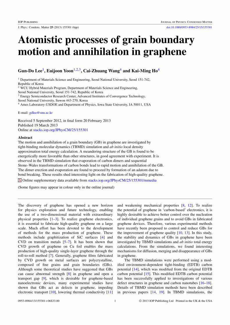
Figure 1. Formation of a unit cell in TBMD simulations (a) and various structures of graphene GBs obtained from the TBMD simulation(b)–(e). The dotted lines in (a) show the lattice mismatch of a (5, 0) zigzag (ZZ) grain and a (3, 3) armchair (AC) grain. The solid lines in (a)show the lattice mismatch of a (7, 0) ZZ grain and a (4, 4) AC grain. The dashed lines in (a) show the lattice mismatch of a (9, 0) ZZ grainand a (5, 5) AC grain. The yellow and blue colors indicate carbon atoms and bonds on hexagonal rings and non-hexagonal rings,respectively. The red solid circles indicate dimers which will undergo SW transformation for the next structure. The green dashed circle in(b) indicates a dimer which undergoes SW transformation for the structural change into (e).
self-consistent calculations are performed by including aHubbard-U term in the TB Hamiltonian to describe correctlycharge transfer in carbon atoms with dangling bonds and toprevent unrealistic overestimation of the charge transfer [20].The equations of motion of the atoms were solved by thefifth order predictor–corrector algorithm with a time step of1.0 fs. All simulations were started at temperature of 3000 Kand the velocity scaling method was used to control thetemperature. The temperature was also gradually increased to5000 K to accelerate the dynamics so that structural changescould be observed during the simulation time. In our TBMD
simulation, we constructed an initial structure of GBs byplacing two zigzag (ZZ) graphene grains with an armchair(AC) graphene grain in between, as shown in figure 1(a).In this case, the AC grain is rotated by 30◦with respect tothe ZZ grains. Such large-angle GBs are frequently found inexperiments [12, 21]. To minimize the strain at the GBs, wefirst examined the lattice mismatches between ZZ grains andAC grains. As shown in figure 1(a), the ZZ (5, 0) grain andthe AC (3, 3) grain have a lattice mismatch of 0.5 A along thedirection parallel to the GB (the y-direction), while the latticemismatch between the ZZ (7, 0) grain and the AC (4, 4) grain
2
J. Phys.: Condens. Matter 25 (2013) 155301 G-D Lee et al
is 0.2 A. In comparison, the lattice mismatch between the ZZ(9, 0) grain and the AC (5, 5) grain is 0.8 A. Therefore, wechose an initial unit cell that contained two ZZ (7, 0) grainsand an AC (4, 4) grain so that the strain from the latticemismatch was the smallest. The unit cell contained 246 atomsand vacuum regions of 30 A in the z direction. Since duringthe TBMD simulation the number of atoms in the unit cellwill be reduced due to the evaporation of carbon dimers, theunit cell dimensions in the graphene plane are also adjustedaccordingly to minimize the stress in unit cell. We have alsocarried out ab initio total energy calculations to verify theTBMD results for the formation energies and energy barriersfor important configurations and their reconstructions. The abinitio calculations were performed within the local densityapproximation (LDA) using the Vienna ab initio simulationpackage (VASP) code [22]. In the calculation, the basis setcontains plane waves up to an energy cutoff of 400 eV, andthe structure is relaxed until the force on each atom is smallerthan 0.02 eV A
−1. The unit cell is also relaxed until the stress
is less than 0.1 kbar.Figure 1(a) shows a relaxed GB structure obtained
from the tight-binding calculation. The GB structure isa meandering structure that is composed of pentagonsand heptagons, as observed in experiments [12, 21]. Wedenote this meandering structure as an ‘M-I’ structure. Fromthis initial GB structure, various additional GB structuresare generated from the TBMD simulations. As shown infigures 1(a) and (b), a Stone–Wales (SW) transformation(90◦ rotation) of a carbon–carbon bond (indicated by a redsolid ellipse in figure 1(a)) leads to another meanderingstructure, ‘M-II’. In comparison with M-I, M-II brings theGB closer to the AC grain. From figures 1(b) to (c),through another SW transformation, the GB structure changesinto a more meandering structure, ‘M-III’, which has alsobeen observed in transmission electron microscopy (TEM)experiments [12, 21]. In figure 1(d), a straight GB structure(S-I) is observed, which is the result of an SW transformation(indicated by a green dotted ellipse in figure 1(c)) from theinitial M-I GB geometry. The S-I structure has been reportedin previous theoretical studies [9, 23, 24]. The formationenergies of the above GB structures were calculated with bothtight-binding and LDA methods. The formation energies [25]of the M-I, M-II, M-III and S-I structures were found to be0.33 (0.37), 0.32 (0.37), 0.46 (0.49) and 0.43 (0.47) eV A
−1,
respectively, by LDA (tight-binding) calculations. The M-IIstructure was found to be more stable than the other structuresand is frequently found in experiments [12, 21].
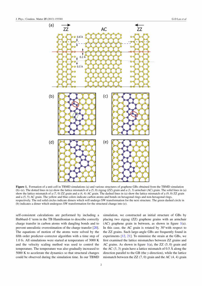
Starting with the stable structure, M-II, we performedTBMD simulations to study the GB structure evolution at hightemperatures (see supplemental video S1 available at stacks.iop.org/JPhysCM/25/155301/mmedia). At the simulationtime of 180 ps at 5000 K, the evaporation of a dimer isobserved, as shown in figure 2(b). In the TBMD simulation,the dimer erection and evaporation are found to proceed bythe formation of an adatom due to bond breaking. We willdiscuss the details of the atomistic process of the carbondimer evaporation in figure 3. After the dimer evaporates,a straight GB structure similar to S-I, shown in figure 1(d),
Figure 2. Snapshots from TBMD simulations for graphene GBs.The distance between two GBs becomes smaller as the simulationproceeds. (a) t = 0.0 ps (t is the simulation time at 5000 K). (b)t = 181.56 ps. (c) t = 186.59 ps. (d) t = 211.15 ps. (e)t = 301.31 ps. (f) t = 498.58 ps. At the bottom, ZZ indicates zigzaggrains and AC indicates armchair grains. The yellow and blue colorsindicate carbon atoms and bonds on hexagonal rings andnon-hexagonal rings, respectively. The red color indicatesevaporated dimers. Green solid ellipses indicate dimers which willundergo SW transformation at the next step. See supplemental videoS1 available at stacks.iop.org/JPhysCM/25/155301/mmedia.
3
J. Phys.: Condens. Matter 25 (2013) 155301 G-D Lee et al
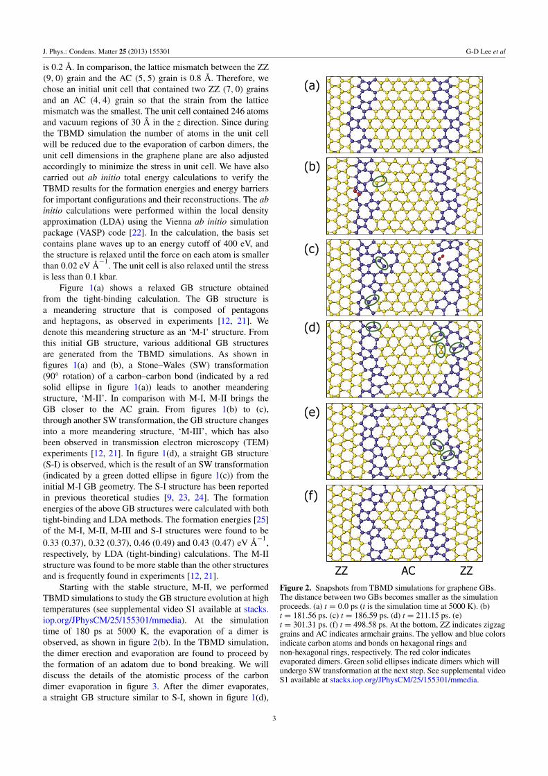
Figure 3. Snapshots from TBMD simulations for dimer evaporation. The numbers show the trajectories of identical atoms. (a) t = 0.0 ps (tis the simulation time at 5000 K). (b) t = 179.52 ps, 1t = 0.0 ps (1t is the elapsed time from (b)). Atom 1 breaks bonds with atoms 3 and10 and diffuses to a bridge site between atoms 2 and 5. (c) 1t = 0.6 ps. Atom 1 diffuses to the bridge site between atoms 5 and 6. (d)1t = 1.2 ps. Atom 1 is pushed down and atom 5 becomes an adatom. The bond between atoms 8 and 9 undergoes an SW transformation.(e) 1t = 1.7 ps. A carbon dimer consisting of atoms 1 and 5 diffuses and forms an erected dimer on atom 7. (f) 1t = 2.0 ps. The dimerevaporates from the graphene. This figure corresponds to figure 2(b). The yellow and blue colors indicate carbon atoms and bonds onhexagonal rings and non-hexagonal rings, respectively. The red color indicates adatoms and an evaporated dimer. See supplemental videoS2 available at stacks.iop.org/JPhysCM/25/155301/mmedia.
is temporarily formed, as shown in figure 2(b). Several SWtransformations lead the GB on the left-hand side to theM-II structure again and to advance toward the AC grain, asshown in figure 2(f). A dimer is also evaporated from theGB on the right-hand side, as shown in figure 2(c). Afterthe reconstruction, several SW transformations also causethe right-hand-side GB to return to the M-II structure anddiffuse toward the AC grain, as shown in figure 2(f). Thetotal energy difference between the structures in figures 2(a)and (f) was found to be 20.2 eV in our LDA calculation.Because two carbon dimers are evaporated in the processfrom figures 2(a) to (f), the LDA calculation result indicatesthat the energy for the evaporation of a dimer from the GBis 10.1 eV, which is much lower than that (18.9 eV) inpristine graphene and is comparable to that (10.6 eV) at theedge of a graphene nanoribbon [19]. It has been shown thatthe structure at a graphene nanoribbon edge is controllablethrough the evaporation of carbon atoms by a Joule heatingprocess [26]. Although our TBMD simulation was performed
at very high temperature (∼5000 K) to save simulation time,it is estimated from the Arrhenius relation that the evaporationof a dimer can be observed in a few seconds at the temperature(∼2800 ◦C) [27] of Joule heating. Accordingly, our simulationresults suggest that GBs could also be controlled through theevaporation of carbon dimers with electron irradiation or athermal annealing process such as Joule heating. Comparingfigure 2(f) with (a), it is clear that two GBs move toward theAC grain, resulting in a reduction in the distance between thetwo GBs. From the simulation results, we suggest that themotion of the GBs prefers certain directions, and the size ofspecific grains can be reduced if the orientation of these grainsmatches the favorable GB motion direction. The evaporationof carbon dimers and the consequent SW transformations giverise to the motion of GBs and cause the GBs to transforminto the stable structure, M-II. From a geometrical point ofview, it is impossible for a GB to maintain the M-II structureand to move solely by SW transformations without dimerevaporation. Therefore, the evaporation of carbon dimers
4
J. Phys.: Condens. Matter 25 (2013) 155301 G-D Lee et al
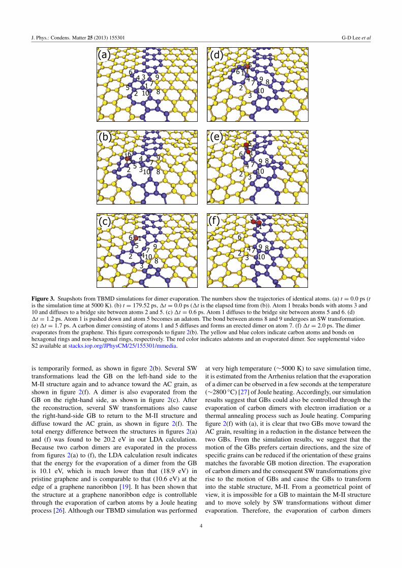
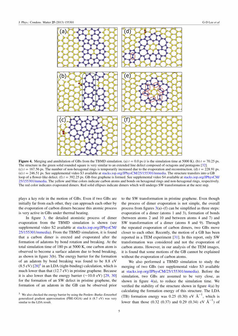
Figure 4. Merging and annihilation of GBs from the TBMD simulation. (a) t = 0.0 ps (t is the simulation time at 5000 K). (b) t = 70.25 ps.The structure in the green solid rounded square is very similar to an extended line defect composed of octagons and pentagons [32].(c) t = 167.56 ps. The number of non-hexagonal rings is temporarily increased due to the evaporation and reconstruction. (d) t = 228.91 ps.(e) t = 246.51 ps. See supplemental video S3 available at stacks.iop.org/JPhysCM/25/155301/mmedia. The structure transfers into a GBloop of a flower-like defect. (f) t = 392.25 ps. GB-free graphene is formed. See supplemental video S4 available at stacks.iop.org/JPhysCM/25/155301/mmedia. The yellow and blue colors indicate carbon atoms and bonds on hexagonal rings and non-hexagonal rings, respectively.The red color indicates evaporated dimers. Red solid ellipses indicate dimers which will undergo SW transformation at the next step.
plays a key role in the motion of GBs. Even if two GBs areinitially far from each other, they can approach each other bythe evaporation of carbon dimers because this atomic processis very active in GBs under thermal heating.
In figure 3, the detailed atomistic process of dimerevaporation from the TBMD simulation is shown (seesupplemental video S2 available at stacks.iop.org/JPhysCM/25/155301/mmedia). From the TBMD simulation, it is foundthat a carbon dimer is erected and evaporated after theformation of adatoms by bond rotation and breaking. At thetotal simulation time of 180 ps at 5000 K, one carbon atom isobserved to become a surface adatom due to bond breaking,as shown in figure 3(b). The energy barrier for the formationof an adatom by bond breaking was found to be 8.8 eV(8.5 eV) [28]5 in an LDA (tight-binding) calculation, which ismuch lower than that (12.7 eV) in pristine graphene. Becauseit is also lower than the energy barrier (∼10.0 eV) [29, 30]for the formation of an SW defect in pristine graphene, theformation of an adatom in the GB can be observed prior
5 We also checked the energy barrier by using the Perdew–Burke–Ernzerhofgeneralized gradient approximation (PBE-GGA) and it (8.7 eV) was verysimilar to the LDA result.
to the SW transformation in pristine graphene. Even thoughthe process of dimer evaporation is not simple, the overallprocess from figures 3(a)–(f) can be simplified as three steps:evaporation of a dimer (atoms 1 and 3), formation of bonds(between atoms 2 and 10 and between atoms 4 and 7) andSW transformation of a dimer (atoms 8 and 9). Throughthe repeated evaporation of carbon dimers, two GBs movecloser to each other. Recently, the motion of a GB has beenreported in a TEM experiment [31]. In this report, only SWtransformation was considered and not the evaporation ofcarbon atoms. However, in our analysis of the TEM images,it is found that some motions of the GB cannot be explainedwithout the evaporation of carbon atoms.
We also performed a TBMD simulation to study themerging of two GBs (see supplemental video S3 availableat stacks.iop.org/JPhysCM/25/155301/mmedia). Before thesimulation, two GBs are assumed to be very close, asshown in figure 4(a), to reduce the simulation time. Weverified the stability of the structure shown in figure 4(a) bycalculating the formation energy of this structure. The LDA(TB) formation energy was 0.25 (0.30) eV A
−1, which is
lower than those (0.32 (0.37) and 0.29 (0.34) eV A−1
) of
5
J. Phys.: Condens. Matter 25 (2013) 155301 G-D Lee et al
the separate GBs in figures 2(a)–(f). As the distance betweenthe GBs decreases, the formation energy is also found todecrease in our LDA and TB calculations. In the TBMDsimulation, the two GBs are found to merge with each otherand are finally annihilated through the sequential evaporationof dimers and SW transformations, as shown in figure 4. Theactive sequential evaporation of carbon dimers at the GBs isclearly shown, which accelerates the merging and annihilationof the GBs. During the simulation, the extended line defect iscomposed of octagons and pentagons, which is very similar tothe line defect structure observed in polycrystalline grapheneon Ni(111) [32], as shown in figure 4(b). At the final stageof the simulation, the structure transfers into a GB loop ofa flower-like defect, as shown in figures 4(d)–(e). It is veryinteresting to observe this GB loop, which has been suggestedin a theoretical study [33], in our TBMD simulation. Thenon-hexagonal rings finally disappear through sequential SWtransformations of six carbon bonds (see supplemental videoS4 available at stacks.iop.org/JPhysCM/25/155301/mmedia),as indicated by the red ellipses in figure 4(e), and GB-freegraphene is formed, as shown in figure 4(f). From the TBMDsimulation, it is found that the two GBs approach eachother, merge, and finally disappear through the evaporationof carbon dimers and sequential SW transformations. It isalso interesting to note that various GB structures observed inexperiments are found in our TBMD simulation. The motionand annihilation of GBs observed in our TBMD simulationare expected to be found in experiments such as TEM studies.These results can also be applied to the control of grainsand GBs in graphene. In this simulation, the trajectory forthe motion and recombination of GBs observed may not bethe only way. More simulations in future work with differentinitial conditions would be needed to clarify the uniquenessof the trajectory. Our simulation structure is a GB structure oflarge angle (30◦) and our conclusions can be drawn from thepeculiar structure of the GB. The same study is also requiredfor various structures of GBs including GBs of small angles.
Acknowledgments
This work was supported by the Brain Korea 21 (BK21)program, World Class University (WCU) program (R31-2008-000-10075-0) of the Ministry of Education of Korea.This work was also supported by the Basic ScienceResearch Program through the National Research Foundationof Korea (NRF) funded by the Ministry of Education,Science and Technology (MEST) (Nos 2012-0003007 and2012-0000904). The authors also acknowledge the supportfrom KISTI under the Strategic Supercomputing ApplicationsSupport Program. The work at Ames Laboratory wassupported by the US Department of Energy, Basic EnergySciences, Division of Materials Science and Engineering,
including a grant of computer time at the National EnergyResearch Supercomputing Centre (NERSC) in Berkeley, CAunder Contract No. DE-AC02-07CH11358.
References
[1] Novoselov K S, Geim A K, Morozov S V, Jiang D, Zhang Y,Dubonos S V, Grigorieva I V and Firsov A A 2004 Science306 666
[2] Novoselov K S, Geim A K, Morozov S V, Jiang D,Katsnelson M I, Grigorieva I V, Dubonos S V andFirsov A A 2005 Nature 438 197
[3] Zhang Y, Tan Y-W, Stormer H L and Kim P 2005 Nature438 201
[4] Emtsev K V et al 2009 Nature Mater. 8 203[5] Reina A, Jia X, Ho J, Nezich D, Son H, Bulovic V,
Dresselhaus M S and Kong J 2008 Nano Lett. 9 30[6] Li X et al 2009 Science 324 1312[7] Bae S et al 2010 Nature Nanotechnol. 5 574[8] Grantab R, Shenoy V B and Ruoff R S 2010 Science 330 946[9] Yazyev O V and Louie S G 2010 Nature Mater. 9 806
[10] Yu Q et al 2011 Nature Mater. 10 443[11] Cai W, Moore A L, Zhu Y, Li X, Chen S, Shi L and
Ruoff R S 2010 Nano Lett. 10 1645[12] Huang P Y et al 2011 Nature 469 389[13] Li X, Magnuson C W, Venugopal A, Tromp R M, Hannon J B,
Vogel E M, Colombo L and Ruoff R S 2011 J. Am. Chem.Soc. 133 2816
[14] Lee G-D, Wang C Z, Yoon E, Hwang N-M and Ho K M 2006Phys. Rev. B 74 245411
[15] Tang M S, Wang C Z, Chan C T and Ho K M 1996 Phys. Rev.B 53 979
[16] Lee G-D, Wang C Z, Yoon E, Hwang N-M, Kim D-Y andHo K M 2005 Phys. Rev. Lett. 95 205501
[17] Lee G-D, Wang C-Z, Yu J, Yoon E, Hwang N-M andHo K-M 2007 Phys. Rev. B 76 165413
[18] Lee G D, Wang C Z, Yoon E, Hwang N M and Ho K M 2010Appl. Phys. Lett. 97 093106
[19] Lee G-D, Wang C Z, Yoon E, Hwang N-M and Ho K M 2010Phys. Rev. B 81 195419
[20] Xu C H, Wang C Z, Chan C T and Ho K M 1992 J. Phys.:Condens. Matter 4 6047
[21] Kim K, Lee Z, Regan W, Kisielowski C, Crommie M F andZettl A 2011 ACS Nano 5 2142
[22] Kresse G and Furthmuller J 1996 Phys. Rev. B 54 11169[23] Liu Y and Yakobson B I 2010 Nano Lett. 10 2178[24] Wang B, Puzyrev Y and Pantelides S T 2011 Carbon 49 3983[25] Yazyev O V and Louie S G 2010 Phys. Rev. B 81 195420[26] Jia X et al 2009 Science 323 1701[27] Jia X T et al 2009 J. Vac. Sci. Technol. B 27 1996[28] Perdew J P, Burke K and Ernzerhof M 1996 Phys. Rev. Lett.
77 3865[29] Dumitrica T and Yakobson B I 2004 Appl. Phys. Lett. 84 2775[30] Li L, Reich S and Robertson J 2005 Phys. Rev. B 72 184109[31] Kurasch S, Kotakoski J, Lehtinen O, Skakalova V, Smet J,
Krill C E, Krasheninnikov A V and Kaiser U 2012 NanoLett. 12 3168
[32] Lahiri J, Lin Y, Bozkurt P, Oleynik I I and Batzill M 2010Nature Nanotechnol. 5 326
[33] Cockayne E, Rutter G M, Guisinger N P, Crain J N,First P N and Stroscio J A 2011 Phys. Rev. B 83 195425
6