Embed Size (px)
Citation preview
LEHTINEN ET AL. VOL. 9 ’ NO. 3 ’ 3274–3283 ’ 2015
www.acsnano.org
3274
March 06, 2015
C 2015 American Chemical Society
Atomic Scale Microstructureand Properties of Se-DeficientTwo-Dimensional MoSe2Ossi Lehtinen,*,† Hannu-Pekka Komsa,‡ Artem Pulkin,§ Michael Brian Whitwick,^ Ming-Wei Chen,^
Tibor Lehnert,† Michael J. Mohn,† Oleg V. Yazyev,§ Andras Kis,^ Ute Kaiser,† and Arkady V. Krasheninnikov )
†Group of Electron Microscopy of Materials Science, Central Facility for Electron Microscopy, University of Ulm, 89081 Ulm, Germany, ‡COMP Centre of Excellence,Department of Applied Physics, Aalto University, P.O. Box 11100, FI-00076 Aalto, Finland, §Institute of Theoretical Physics, Ecole Polytechnique Fédérale deLausanne (EPFL), CH-1015 Lausanne, Switzerland, ^Electrical Engineering Institute, Ecole Polytechnique Fédérale de Lausanne (EPFL), CH-1015 Lausanne,Switzerland, and )Department of Applied Physics, Aalto University, P.O. Box 11100, FI-00076 Aalto, Finland
Altering the atomic composition of amaterial away from its perfect stoi-chiometric ratio is a standard ap-
proach for tailoring its properties. Perhapsthe most famous example is the rich phasediagram of the Fe�Fe3C system, wherematerials with diverse characteristics canbe manufactured by varying the composi-tion and the growth history.1 One can ex-pect that the same approach should alsowork for two-dimensional (2D) systems.However, engineering of 2D materials bydeviations from the 'perfect' stoichiometricbalance between the primary componentsis a largely unexplored topic to this date.This is particularly relevant to 2D transi-
tionmetal dichalcogenides (TMDs). Recently,significant efforts have been directed to-ward producing 2D TMDs, due to theirintriguing electronic properties,2 with vari-ations of the chemical vapor deposition
(CVD) technique3�9 being the most promis-ing in terms of large-scale production. Thetypical aim of such efforts has been theproduction of high-quality crystals at theperfect 1:2 stoichiometric composition, or 2DTMD random alloys ternary compounds10,11
with mixing either in the chalcogen12�14 ormetal15,16 sublattice. However, defects anddopant atoms can also be used to modifythe properties of these materials.17�24 Re-cently, Kim et al.25 studied the influence ofnonstoichiometry on the transport prop-erties of CVD 2D MoS2�x sheets and foundincreased mobilities in connection with aS-deficit, demonstrating the feasibility ofengineering of 2D TMDs by moving awayfrom the stoichiometric composition. More-over, the thermoelectric properties, chargecarrier concentrations26 and mass density27
of bulk MoSe2 are influenced by small devia-tions from the stoichiometric composition.
* Address correspondence [email protected].
Received for review January 19, 2015and accepted March 6, 2015.
Published online10.1021/acsnano.5b00410
ABSTRACT We study the atomic scale microstructure of non-
stoichiometric two-dimensional (2D) transition metal dichalcogenide
MoSe2�x by employing aberration-corrected high-resolution trans-
mission electron microscopy. We show that a Se-deficit in single
layers of MoSe2 grown by molecular beam epitaxy gives rise to a
dense network of mirror-twin-boundaries (MTBs) decorating the 2D-
grains. With the use of density functional theory calculations, we
further demonstrate that MTBs are thermodynamically stable
structures in Se-deficient sheets. These line defects host spatially localized states with energies close to the valence band minimum, thus giving rise
to enhanced conductance along straight MTBs. However, electronic transport calculations show that the transmission of hole charge carriers across MTBs is
strongly suppressed due to band bending effects. We further observe formation of MTBs during in situ removal of Se atoms by the electron beam of the
microscope, thus confirming that MTBs appear due to Se-deficit, and not coalescence of individual grains during growth. At a very high local Se-deficit, the
2D sheet becomes unstable and transforms to a nanowire. Our results on Se-deficient MoSe2 suggest routes toward engineering the properties of 2D
transition metal dichalcogenides by deviations from the stoichiometric composition.
KEYWORDS: 2D TMD . microstructure . stoichiometry . HRTEM . MBE . CVD . DFT . defects
ARTIC
LE
LEHTINEN ET AL. VOL. 9 ’ NO. 3 ’ 3274–3283 ’ 2015
www.acsnano.org
3275
Thus, as controlled composition engineering of thematerials can take place only when the atomic scalemorphology resulting from a given growth process canbe predicted, microscopic information on the exactatomic structure of nonstoichiometric samples is essen-tial for theoptimizationof growthprocess and completeunderstanding of the behavior of the new materials.In terms of the phase diagram of the 2D TMDs, the
reduced dimensionality imposes a strong limitationon the useful range of compositions; however onlysome distinct phases, such as the hexagonal 2H,rhombohedral 3R, and tetragonal 1T structures ofTMDs, are layered and thus can form stable/metastable2D structures.28 Moving down in Se-content in theMo�Se bulk system, for example, leads eventually tothe crossing of the MoSe2�Mo3Se4 phase boundaryand the crystal structure becoming three-dimensional.Here, we explore the atomic scale microstructure of
Se-deficient 2D MoSe2�x sheets, where the 2D topol-ogy is retained despitemoving away from the stoichio-metric composition. We investigate single layer 2DMoSe2�x grown by molecular beam epitaxy (MBE)using aberration-corrected high-resolution transmis-sion electron microscopy (AC-HRTEM) at 80 kV. Theinvestigated material is found to be a nanocrystallinefilm with a MoSe1.983(1) in-grain composition. TheMo�Se imbalance is manifested as mirror-twin-boundaries (MTB) decorating individual grains, andthe composition can be determined by measuringthe areal density of the MTBs in AC-HRTEM images.Our calculations based on the density functionaltheory (DFT) indicate that such a configuration isenergetically favorable in Se-deficient conditions. Thecalculated electronic band structure of the experimen-tally observed MTB presents evidence for localizedstates in a wide energy range in the semiconductorgap near the bottom of the conduction band. Ourcalculations of the ballistic electronic transport usingthe nonequilibrium Green's function approach acrossthe MTB defect shows high transmission for the elec-tron charge carriers, but low conductivity for the holes.We further demonstrate the formation of such bound-aries in situ, when the electron beam of the TEMgradually removes Se atoms from the lattice andeventually the lattice spontaneously reorganizeslocally into a mirror-domain. With further removal ofSe, the 2D sheet is transformed into a nanowire, that is,a 2D to 1D transition is observed.
RESULTS AND DISCUSSION
Single layer 2D MoSe2 samples were grown in acustomized MBE system, and the as-grown films weretransferred onto TEM grids using poly(methylmethacrylate) (PMMA) as a temporary support, asdescribed in more detail in the Materials and Meth-ods section. The samples were then investigated inan aberration-corrected high-resolution transmission
electron microscope (FEI Titan 80�300), operatedat 80 kV.At first impression, the sample was observed to
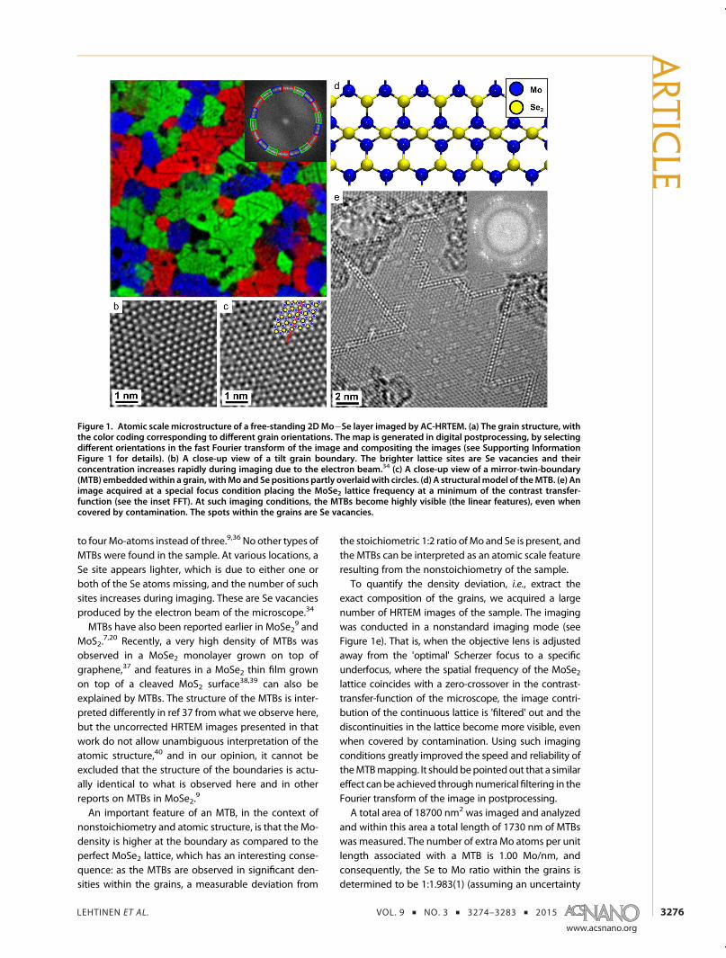
consist of a free-standing membrane of single layerMoSe2 with a very fine grain-structure (only few smallmultilayer patches are present, as confirmed by ex-tensive survey of the material using HRTEM, see Sup-porting Information Figure 4). A 130 nm� 130 nm areais shown in Figure 1a with color coding applied tohighlight grain distributions and orientations withinthe membrane (see Supporting Information Figure 1and ref 29 for details on the generation of such animage). All the grains have the basal plane alignedwiththe membrane surface, but have seemingly randomin-plane orientations, and the grains have diameters inthe range of few tens of nanometers. The grains arestitched together by tilt-grain-boundaries consistingof rows of dislocations (Figure 1 b), similar to whathas been observed earlier for MoSe2,
9 MoS2,6,20 and
graphene.30�33 The small size of the grains can betentatively explained by a high density of nucleationsites during growth of the membrane.However, close examination of the images indicated
that individual grains have additional structure. Thegrains consist of the regular trigonal MoSe2 latticedecorated by another type of very straight boundariesrunning through the grains, making sharp turns andoccasionally forming closed triangular loops (theseboundaries become also visible as a side effect of theorientation mapping, see Figure 1a). In Figure 1c, thepositions of the Mo and the dual Se atoms are partlyoverlaid in the AC-HRTEM image, where the darkestspots correspond to the Se sites (i.e., dark atomcontrast), the lighter spots to single Mo atoms, andthe bright spots to the empty centers of the hexagons.On the basis of the identification of the atom positions(see also simulated image in Supporting InformationFigure 5), the boundaries can be identified as mirror-twin-boundaries (MTBs), or, equivalently, as 60/180/300� tilt grain boundaries, where the leading Se edgesof two adjacent MoSe2 lattices meet (see Figure 1dfor the structural model). With respect to edge typeclassification, we use the standard nomenclature.35
The Se- and Mo-edges are shown in Supporting In-formation Figure 4a, and they are classified accordingto the atom types at the zigzag edge just after cuttingthe ideal lattice, independent ofwhat kind of atoms arelater on attached to the edge (e.g., the Mo edge mayhave zero, one or two Se atoms attached to the edgeMo atoms). The lattice on the opposite sides of theseboundaries has seemingly the same orientation, butwith an important distinction: the trigonal MoSe2lattice is mirrored across the boundary, that is, theMo and the dual Se sites are interchanged. Whilethe Se-sublattice continues uninterrupted over theboundary, the Mo-sublattice has a discontinuity attheMTB resulting in Se-atoms at the boundary binding
ARTIC
LE
LEHTINEN ET AL. VOL. 9 ’ NO. 3 ’ 3274–3283 ’ 2015
www.acsnano.org
3276
to four Mo-atoms instead of three.9,36 No other types ofMTBs were found in the sample. At various locations, aSe site appears lighter, which is due to either one orboth of the Se atoms missing, and the number of suchsites increases during imaging. These are Se vacanciesproduced by the electron beam of the microscope.34
MTBs have also been reported earlier in MoSe29 and
MoS2.7,20 Recently, a very high density of MTBs was
observed in a MoSe2 monolayer grown on top ofgraphene,37 and features in a MoSe2 thin film grownon top of a cleaved MoS2 surface38,39 can also beexplained by MTBs. The structure of the MTBs is inter-preted differently in ref 37 from what we observe here,but the uncorrected HRTEM images presented in thatwork do not allow unambiguous interpretation of theatomic structure,40 and in our opinion, it cannot beexcluded that the structure of the boundaries is actu-ally identical to what is observed here and in otherreports on MTBs in MoSe2.
9
An important feature of an MTB, in the context ofnonstoichiometry and atomic structure, is that the Mo-density is higher at the boundary as compared to theperfect MoSe2 lattice, which has an interesting conse-quence: as the MTBs are observed in significant den-sities within the grains, a measurable deviation from
the stoichiometric 1:2 ratio ofMo and Se is present, andthe MTBs can be interpreted as an atomic scale featureresulting from the nonstoichiometry of the sample.To quantify the density deviation, i.e., extract the
exact composition of the grains, we acquired a largenumber of HRTEM images of the sample. The imagingwas conducted in a nonstandard imaging mode (seeFigure 1e). That is, when the objective lens is adjustedaway from the 'optimal' Scherzer focus to a specificunderfocus, where the spatial frequency of the MoSe2lattice coincides with a zero-crossover in the contrast-transfer-function of the microscope, the image contri-bution of the continuous lattice is 'filtered' out and thediscontinuities in the lattice become more visible, evenwhen covered by contamination. Using such imagingconditions greatly improved the speed and reliability oftheMTBmapping. It should bepointed out that a similareffect can be achieved throughnumericalfiltering in theFourier transform of the image in postprocessing.A total area of 18700 nm2 was imaged and analyzed
and within this area a total length of 1730 nm of MTBswas measured. The number of extra Mo atoms per unitlength associated with a MTB is 1.00 Mo/nm, andconsequently, the Se to Mo ratio within the grains isdetermined to be 1:1.983(1) (assuming an uncertainty
Figure 1. Atomic scale microstructure of a free-standing 2DMo�Se layer imaged by AC-HRTEM. (a) The grain structure, withthe color coding corresponding to different grain orientations. The map is generated in digital postprocessing, by selectingdifferent orientations in the fast Fourier transform of the image and compositing the images (see Supporting InformationFigure 1 for details). (b) A close-up view of a tilt grain boundary. The brighter lattice sites are Se vacancies and theirconcentration increases rapidly during imaging due to the electron beam.34 (c) A close-up view of a mirror-twin-boundary(MTB) embeddedwithin a grain, withMo and Se positions partly overlaidwith circles. (d) A structuralmodel of theMTB. (e) Animage acquired at a special focus condition placing the MoSe2 lattice frequency at a minimum of the contrast transfer-function (see the inset FFT). At such imaging conditions, the MTBs become highly visible (the linear features), even whencovered by contamination. The spots within the grains are Se vacancies.
ARTIC
LE
LEHTINEN ET AL. VOL. 9 ’ NO. 3 ’ 3274–3283 ’ 2015
www.acsnano.org
3277
of (100 nm in the measured total MTB length). Themass density of the material was calculated to be0.32(2)% higher than perfect MoSe2, keeping in mindthat the Mo density is increased at the MTBs. The tilt-grain-boundaries can be Mo- or Se-rich36 as well. How-ever, our analysis is limited to the in-grain composition,excluding the edges of the grains, and thus the composi-tion of the tilt-boundaries is not accounted for. As alreadymentioned, a high density of Se-vacancies is also visiblein the HRTEM images. This can be attributed to genera-tion of vacancies by the electron beam during imaging34
as discussed later, and is thus not accounted for in thecomposition determination of the pristine material.Although observation of the atomic structure during
growth is not possible, insights into the growth historyand thus the origin of the MTBs can be gained byanalyzing the observed structures. Two possible scenar-ios can be imagined for forming the MTBs duringgrowth (postgrowth formation is discussed later). First,the observed type ofMTBs can formwhen two adjacentgrains merge. This requires (a) that the grains grow inthe direction of the leading Se-edge, and (b) that themistilt of the twomerging grains is close to 180� (due tothe trigonal symmetry of the lattice, mistilts of 60� and300� are equal to 180�). Second, the MTBs could formduring the growth of individual grains, where, e.g.,formation ofMTBswould be initiated during the growthof the grain and the growth would continue with anMTB extending in the growth direction.For assessing the validity of the first scenario, we can
look at the distribution of the grain orientations, and thefrequency at which MTBs are observed as compared toother tilt boundaries. No preferred orientation of indivi-dual grains is found (see Supporting InformationFigure2),which means we should have a uniform distribution ofmistilt angles of the grain boundaries. Thus, the hy-phothesis of MTB formation through merging of grow-ing adjacent grains can be tested by looking at themistilt angle distribution in the sample. According toearlier calculations,20 the grain boundary energydecreases within a 10� deviation from the optimal180� orientation, and if we assume that grains meetingwithin this range reorient to optimize the energy andform MTBs, the expected fraction of MTBs among allgrain boundaries is one in six. However, a density of0.097(6) nm/nm2 of tilt-grain boundaries is observed inthe sample, which is almost identical to the density ofMTBs (0.093(5) nm/nm2), meaning that the MTBs areoverrepresented. For a one-to-one ratio between othertilt-boundaries and MTBs, formation of MTBs shouldtake place at up to (30� deviation from the ideal 180�tilt, and even if few degree mistilts over the MTBs areoccasionally seen in the sample (see for example thelower left MTB in Figure 1e), high mistilts over MTBs ofup to 30� are never observed. On the basis of this,formation of the MTBs simply due to merging of mis-oriented neighboring grains can be ruled out.
As formation due to merging of grains does notseem to be a plausible explanation for the appearanceof the MTBs, we need to look into the second scenario:Formation of MTBs during the growth of individualgrains. Here, formation of MTBs would be initiatedduring the growth of the grain and the growth wouldcontinue with an MTB extending in the growth direc-tion. As shown below by our DFT calculations, movingto Mo-rich growth conditions significantly lowers theformation energy of MTBs, giving rise to an increaseddensity during growth. Also, Se has a low stickingcoefficient,41,42 which can result in a local Se-deficiteven at excess deposition rates. Locations in thesample with multiple MTBs radially emanating fromthe same point in a star like pattern are observed (seeSupporting Information Figure 3a), which can be inter-preted as nucleation sites of the grains, supporting thehyphothesis of formation of MTBs during grain growthin the growth direction. Currently, precise control ofthis process is not possible, however, and further workis necessary to enable controlled growth of MTBsembedded in larger crystallites.An additional insight into the growth history can be
gained from the boundary statistics: asMTBswhere theleading Mo-edges of the grains meet (see the struc-tures 4�6 in Figure 2a) are never observed in thesample, the grain growth can be deduced to havetaken place in the leading Se-edge direction. As dis-cussed in more detail in the Supporting Information,our DFT calculations show that, indeed, the environ-ment influences the energetics of different edge ter-minations, with the leading Se-edge being the lowestenergy configuration in a Mo-rich environment, whilethe leading Mo-edge is preferred at Se-rich conditions(see Supporting Information for details).Until now, we have observed a specific kind of atomic
scale microstructure associated with a deviation fromthe perfect 1:2Mo�Se ratio in the sample, namelyMTBsembedded within the grains. To learn whether this isactually the preferred microstructure within the 2DMo�Se phase diagram when moving down in Se con-tent from the stoichiometric 1:2 ratio,we conductedDFTcalculations, determining the energetics of a number ofdefect structures with a Se-deficit.We start by considering the relative energies of
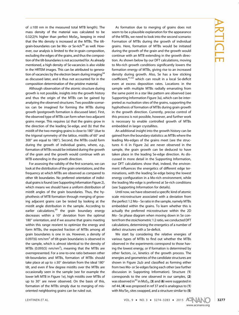
various types of MTBs to find out whether the MTBsobserved in the experiments correspond to those hav-ing the lowest energy, or if formation is determined byother factors, i.e., kinetics of the growth process. Theenergies and geometries of the candidate structures areshown in Figure 2a,b and classified as forming eitherfrom twoMo- or Se-edges facing each other (see furtherdiscussion in Supporting Information). Structure (1)corresponds to the one observed in our samples, (2)was observed in43 inMoS2, (3) and (6) were suggested inref 44, (4) was proposed in ref 37 and is analogous to (1)withMo/Se2 sites swapped, and a structure similar to (5)
ARTIC
LE
LEHTINEN ET AL. VOL. 9 ’ NO. 3 ’ 3274–3283 ’ 2015
www.acsnano.org
3278
was suggested in ref 36 (although we found that ourstructure with the two domains shifted by half a latticeconstant along the boundary is lower in energy by0.6 eV). The calculations are carried out in a ribbongeometry. The formation energy is defined as
Ef ¼ E(MTB) � (nMoμMoþ nSeμSe þ 2γ) (1)
where E(MTB) is the total energy from the supercellcalculation and γ is the edge energy (see SupportingInformation). nSe and nMo are the numbers of Se andMoatoms in the supercell. Chemical potentials μMo and μSeare determined through the condition of the equilibri-umwithMoSe2:μMoþ 2μSe = E(MoSe2) (where E(MoSe2)is the energy from a primitive cell of MoSe2), and limitedby theMo bulk phase in the Mo-rich end and by the Se8molecule on the Se-rich end. Among the candidates,structure (1) has the lowest energy by a fairly largemarginof 0.3 eV, but allMTB structures constructed fromSe-edges seem to be favored over thosewithMo-edges.We also estimated the MTB formation energy by con-structing supercells with triangular mirror domains(similar to that shown in Figure 4). The formation energyfor structure (1) at the Mo-rich limit is 0.12 eV, about0.2 eV higher than that from the ribbon calculation,which can be assigned to differences in relaxation andon the position of the Fermi-level in the system.We also considered vacancy line structures, similar
to what we have previously observed in MoS2,19,45
where the lineswere found tobeenergetically favorable,
as compared to isolated vacancies. Their formationenergies are also shown in Figure 2b but are found tobe much higher than those for the MTBs for the wholerange of chemical potentials.Reports in literature concerning the phase diagram
of Mo/Se systems are scarce. MoSe2 and Mo3Se4are known to be stable phases, but the behavior atthe intermediate stoichiometries appears to be un-known.46 Thus, the question, whether the MTB-richstructures are lower in energy than a system withcoexisting MoSe2/Mo3Se4 phases, needs to be an-swered. In Figure 2c, we plot heat of formation H forall these systems as a function of their Se/Mo content.As usual, it is defined asH= E� nMoμMo� nSeμSe, whereE is the total energy of the system composed from nMo
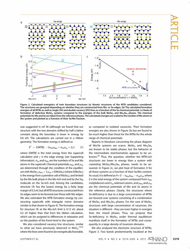
molybdenumand nSe seleniumatoms, and μMo and μSeare the chemical potentials of Mo and Se atoms inthe reference phases. Clearly, the structures whereSe-deficiency is due to a large concentration of MTBsare favored over systems consisting of a combinationof MoSe2 and Mo3Se4 phases. For the case of MoSe2structures with large concentration of vacancies, thesituation is different�they are even higher in energiesthan the mixed phases. Thus, we propose thatSe-deficiency in MoSe2 under thermal equilibriummanifests itself in the formation of MTBs and conse-quently in a large density of inversion domains.We also analyzed the electronic structure of MTBs,
Figure 3. Two bands predominantly localized at the
Figure 2. Calculated energetics of twin boundary structures (a) Atomic structures of the MTB candidates considered.The structures are grouped depending on whether they are constructed fromMo- or Se-edges. (b) The calculated formationenergies of all MTBs as well as single (SV) and double vacancy (DV) lines as a function of the Se chemical potential. (c) Heats offormation of defective MoSe2 systems compared to the energies of the bulk MoSe2 and Mo3Se4 phases. The chemicalpotentials forMoandSe are taken from the referencephases. The calculated energies are scaled to thenumber ofMoatoms inthe system and plotted as a function of their Se/Mo fraction.
ARTIC
LE
LEHTINEN ET AL. VOL. 9 ’ NO. 3 ’ 3274–3283 ’ 2015
www.acsnano.org
3279
MTB can be distinguished. The squared absolute valueof the wave functions indicate that both are derivedfrom the surrounding Mo atoms. The additional den-sity of states brought in from these bands covers awideenergy range within the gap that could be suggestiveof higher conductivity along the MTBs, at least forstraight periodic boundaries. In amore realistic picture,one has to include also backscattering of 1D conduc-tance channels on the turns and junctions of domainboundaries. There is a chance that such scatteringeffects would considerably reduce the conductancedue to the extra channels. Suppression of localizedelectronic states at the turns of periodic grain bound-aries has recently been observed in epitaxial polycrys-talline graphene grown on the SiC substrate.47 Indeed,our electrical measurements (to be published in an-other article) performed on the samples showed noimprovement, either due to this effect or to the highdensity of tilt-grain-boundaries in the sample, whichmay dominate the transport characteristics of thesample due to increased scattering.7
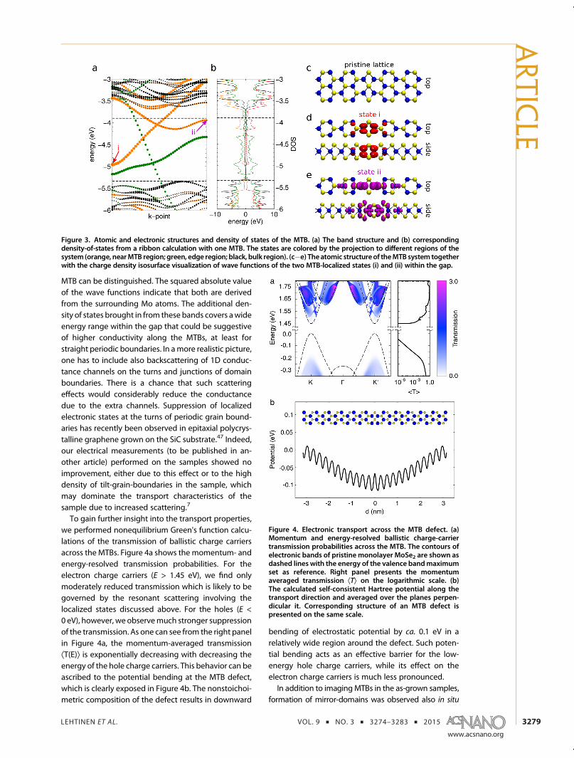
To gain further insight into the transport properties,we performed nonequilibrium Green's function calcu-lations of the transmission of ballistic charge carriersacross the MTBs. Figure 4a shows the momentum- andenergy-resolved transmission probabilities. For theelectron charge carriers (E > 1.45 eV), we find onlymoderately reduced transmission which is likely to begoverned by the resonant scattering involving thelocalized states discussed above. For the holes (E <0 eV), however, we observemuch stronger suppressionof the transmission. As one can see from the right panelin Figure 4a, the momentum-averaged transmissionÆT(E)æ is exponentially decreasing with decreasing theenergy of the hole charge carriers. This behavior can beascribed to the potential bending at the MTB defect,which is clearly exposed in Figure 4b. The nonstoichoi-metric composition of the defect results in downward
bending of electrostatic potential by ca. 0.1 eV in arelatively wide region around the defect. Such poten-tial bending acts as an effective barrier for the low-energy hole charge carriers, while its effect on theelectron charge carriers is much less pronounced.In addition to imagingMTBs in the as-grown samples,
formation of mirror-domains was observed also in situ
Figure 3. Atomic and electronic structures and density of states of the MTB. (a) The band structure and (b) correspondingdensity-of-states from a ribbon calculation with one MTB. The states are colored by the projection to different regions of thesystem (orange, nearMTB region; green, edge region; black, bulk region). (c�e) Theatomic structureof theMTB system togetherwith the charge density isosurface visualization of wave functions of the two MTB-localized states (i) and (ii) within the gap.
Figure 4. Electronic transport across the MTB defect. (a)Momentum and energy-resolved ballistic charge-carriertransmission probabilities across the MTB. The contours ofelectronic bands of pristine monolayer MoSe2 are shown asdashed lines with the energy of the valence bandmaximumset as reference. Right panel presents the momentumaveraged transmission ÆTæ on the logarithmic scale. (b)The calculated self-consistent Hartree potential along thetransport direction and averaged over the planes perpen-dicular it. Corresponding structure of an MTB defect ispresented on the same scale.
ARTIC
LE
LEHTINEN ET AL. VOL. 9 ’ NO. 3 ’ 3274–3283 ’ 2015
www.acsnano.org
3280
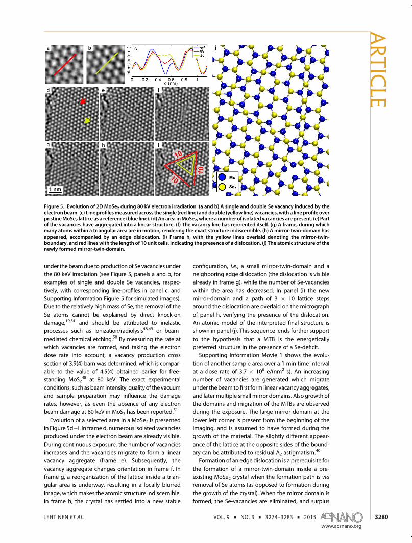
under thebeamdue toproductionof Se vacancies underthe 80 keV irradiation (see Figure 5, panels a and b, forexamples of single and double Se vacancies, respec-tively, with corresponding line-profiles in panel c, andSupporting Information Figure 5 for simulated images).Due to the relatively high mass of Se, the removal of theSe atoms cannot be explained by direct knock-ondamage,19,34 and should be attributed to inelasticprocesses such as ionization/radiolysis48,49 or beam-mediated chemical etching.50 By measuring the rate atwhich vacancies are formed, and taking the electrondose rate into account, a vacancy production crosssection of 3.9(4) barn was determined, which is compar-able to the value of 4.5(4) obtained earlier for free-standing MoS2
48 at 80 keV. The exact experimentalconditions, suchasbeamintensity, quality of the vacuumand sample preparation may influence the damagerates, however, as even the absence of any electronbeam damage at 80 keV in MoS2 has been reported.51
Evolution of a selected area in a MoSe2 is presentedin Figure 5d�i. In framed, numerous isolated vacanciesproduced under the electron beam are already visible.During continuous exposure, the number of vacanciesincreases and the vacancies migrate to form a linearvacancy aggregate (frame e). Subsequently, thevacancy aggregate changes orientation in frame f. Inframe g, a reorganization of the lattice inside a trian-gular area is underway, resulting in a locally blurredimage, whichmakes the atomic structure indiscernible.In frame h, the crystal has settled into a new stable
configuration, i.e., a small mirror-twin-domain and aneighboring edge dislocation (the dislocation is visiblealready in frame g), while the number of Se-vacancieswithin the area has decreased. In panel (i) the newmirror-domain and a path of 3 � 10 lattice stepsaround the dislocation are overlaid on the micrographof panel h, verifying the presence of the dislocation.An atomic model of the interpreted final structure isshown in panel (j). This sequence lends further supportto the hypothesis that a MTB is the energeticallypreferred structure in the presence of a Se-deficit.Supporting Information Movie 1 shows the evolu-
tion of another sample area over a 1 min time intervalat a dose rate of 3.7 � 106 e/(nm2 s). An increasingnumber of vacancies are generated which migrateunder thebeam to first form linear vacancy aggregates,and latermultiple small mirror domains. Also growth ofthe domains and migration of the MTBs are observedduring the exposure. The large mirror domain at thelower left corner is present from the beginning of theimaging, and is assumed to have formed during thegrowth of the material. The slightly different appear-ance of the lattice at the opposite sides of the bound-ary can be attributed to residual A2 astigmatism.40
Formation of an edge dislocation is a prerequisite forthe formation of a mirror-twin-domain inside a pre-existing MoSe2 crystal when the formation path is viaremoval of Se atoms (as opposed to formation duringthe growth of the crystal). When the mirror domain isformed, the Se-vacancies are eliminated, and surplus
Figure 5. Evolution of 2D MoSe2 during 80 kV electron irradiation. (a and b) A single and double Se vacancy induced by theelectronbeam. (c) Lineprofilesmeasured across the single (red line) anddouble (yellow line) vacancies, with a line profile overpristineMoSe2 lattice as a reference (blue line). (d) An area inMoSe2,where a number of isolated vacancies are present. (e) Partof the vacancies have aggregated into a linear structure. (f) The vacancy line has reoriented itself. (g) A frame, during whichmany atoms within a triangular area are in motion, rendering the exact structure indiscernible. (h) A mirror-twin-domain hasappeared, accompanied by an edge dislocation. (i) Frame h, with the yellow lines overlaid denoting the mirror-twin-boundary, and red lines with the length of 10 unit cells, indicating the presence of a dislocation. (j) The atomic structure of thenewly formed mirror-twin-domain.
ARTIC
LE
LEHTINEN ET AL. VOL. 9 ’ NO. 3 ’ 3274–3283 ’ 2015
www.acsnano.org
3281
Mo is introduced at the MTBs. The extra atoms areattained by 'pulling' the neighboring crystal latticetoward the new mirror domain, which leads to theformation of the dislocation. In the presented case, ahole in the MoSe2 crystal close to the newly createddislocation allowed the dislocation to formwithout theformation of a complementary oppositely orienteddislocation, which would be required in the generalcase of a continuous crystal. Importantly, closed MTBloops without an associated dislocation are observedin the as-grown samples (see Supporting InformationFigure 3b), which precludes formation of such domainsin the pristine sample from Se vacancies after growth.Many of theMTBs donot form closed loops, however,
and thus, this kind of analysis is not possible in all thecases. Still, appearance of the MTBs observed already atthe beginning of the imaging due to electron beamremoval of Se does not seem likely. First, the mirrorboundaries are in place already when imaging at lowmagnifications, and consequently, low dose-rates/Sevacancy concentrations. Second, the mirror domainsand MTBs formed under the electron beam have muchsmaller dimensions and are typically connected to otherextensive disorder in the lattice as compared to therelatively long and regular MTBs observed from thebeginning, suggesting a different origin. SupportingInformation Movie 1 shows the generally disorderedstate of the lattice at the time when the new mirrordomains start appearing due to the electron beam.Another comprehensive reorganization of the crystal
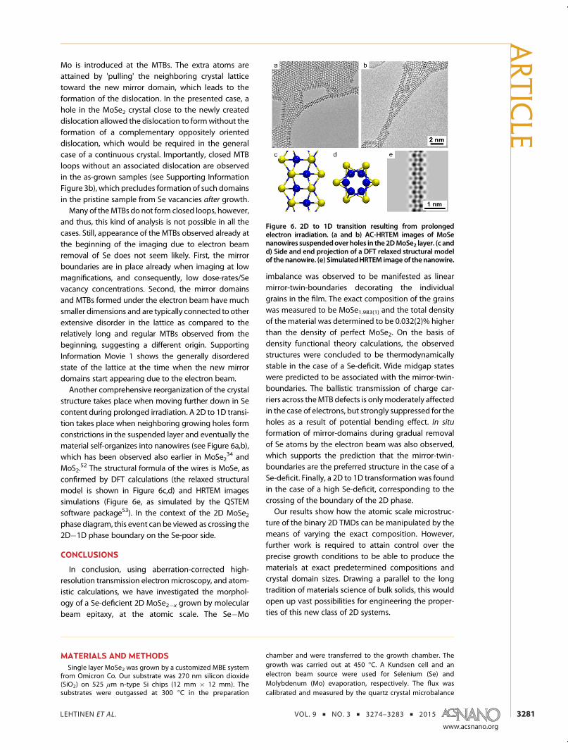
structure takes place when moving further down in Secontent during prolonged irradiation. A 2D to 1D transi-tion takes place when neighboring growing holes formconstrictions in the suspended layer and eventually thematerial self-organizes into nanowires (see Figure 6a,b),which has been observed also earlier in MoSe2
34 andMoS2.
52 The structural formula of the wires is MoSe, asconfirmed by DFT calculations (the relaxed structuralmodel is shown in Figure 6c,d) and HRTEM imagessimulations (Figure 6e, as simulated by the QSTEMsoftware package53). In the context of the 2D MoSe2phase diagram, this event can be viewed as crossing the2D�1D phase boundary on the Se-poor side.
CONCLUSIONS
In conclusion, using aberration-corrected high-resolution transmission electronmicroscopy, and atom-istic calculations, we have investigated the morphol-ogy of a Se-deficient 2D MoSe2�x grown by molecularbeam epitaxy, at the atomic scale. The Se�Mo
imbalance was observed to be manifested as linearmirror-twin-boundaries decorating the individualgrains in the film. The exact composition of the grainswas measured to be MoSe1.983(1) and the total densityof the material was determined to be 0.032(2)% higherthan the density of perfect MoSe2. On the basis ofdensity functional theory calculations, the observedstructures were concluded to be thermodynamicallystable in the case of a Se-deficit. Wide midgap stateswere predicted to be associated with the mirror-twin-boundaries. The ballistic transmission of charge car-riers across theMTBdefects is onlymoderately affectedin the case of electrons, but strongly suppressed for theholes as a result of potential bending effect. In situ
formation of mirror-domains during gradual removalof Se atoms by the electron beam was also observed,which supports the prediction that the mirror-twin-boundaries are the preferred structure in the case of aSe-deficit. Finally, a 2D to 1D transformation was foundin the case of a high Se-deficit, corresponding to thecrossing of the boundary of the 2D phase.Our results show how the atomic scale microstruc-
ture of the binary 2D TMDs can be manipulated by themeans of varying the exact composition. However,further work is required to attain control over theprecise growth conditions to be able to produce thematerials at exact predetermined compositions andcrystal domain sizes. Drawing a parallel to the longtradition of materials science of bulk solids, this wouldopen up vast possibilities for engineering the proper-ties of this new class of 2D systems.
MATERIALS AND METHODSSingle layer MoSe2 was grown by a customized MBE system
from Omicron Co. Our substrate was 270 nm silicon dioxide(SiO2) on 525 μm n-type Si chips (12 mm � 12 mm). Thesubstrates were outgassed at 300 �C in the preparation
chamber and were transferred to the growth chamber. Thegrowth was carried out at 450 �C. A Kundsen cell and anelectron beam source were used for Selenium (Se) andMolybdenum (Mo) evaporation, respectively. The flux wascalibrated and measured by the quartz crystal microbalance
Figure 6. 2D to 1D transition resulting from prolongedelectron irradiation. (a and b) AC-HRTEM images of MoSenanowires suspendedoverholes in the2DMoSe2 layer. (c andd) Side and end projection of a DFT relaxed structural modelof the nanowire. (e) SimulatedHRTEM image of the nanowire.
ARTIC
LE
LEHTINEN ET AL. VOL. 9 ’ NO. 3 ’ 3274–3283 ’ 2015
www.acsnano.org
3282
with a Mo/Se flux ratio ∼1:30. Reflection high-energy electrondiffraction (RHEED) was used to monitor in situ the formationof the crystalline structure during growth. Continuous liquidnitrogen was flowing during the ramping temperature andgrowth phase, with a base pressure of growth chamber at∼10�10 mB.To prepare samples for TEM characterization, the as-grown
filmswere first coatedwith∼500 nm PMMA, andwere cured at180 �C for 5 min. PMMA-embedded films were then lifted off in30% KOH(aq) at 60 �C. The samples were then transferred into adeionized water (DI) bath, and TEM grids were put underneathin order to well-attach the floating films. The grids with theattached films atop were then baked at 60 �C to gentlyvaporize water and also to relieve wrinkles. After completelydrying out, samples were dipped into acetone to removePMMA residues and were rinsed by DI afterward.AC-HRTEM characterization was conducted using an FEI
Titan 80-300 microscope equipped with an image side hexa-pole spherical aberration corrector. The microscope was op-erated at 80 kV, and the extraction voltage of the field emissiongun was lowered to 2 kV in order to reduce the energy spreadof the beam. The spherical aberration coefficient was cor-rected to <20 μm, and the imaging was done at negativedefocus, resulting in atoms appearing as dark spots.Density-functional theory calculations were carried out in
the plane-wave basis and within the projector-augmentedwave (PAW) description of the core regions, as implementedin the VASP code.54,55 We adopt the exchange-correlationfunctional proposed by Perdew, Burke, and Ernzerhof(PBE).56 A 500 eV cutoff and 12 k-points along the periodicdimension(s) yield converged total energies. Our calculationsaccounted for the spin polarization while the spin�orbitinteraction was neglected. The ballistic charge-carrier trans-mission was calculated using the nonequilibrium Green'sfunction technique within the DFT framework as implementedin OpenMX code.57,58 The Hamiltonian was expressed in thelocalized pseudoatomic basis set (Mo:s2p2d2f1, Se:s2p1d1f1).The length of rectangular scattering region containing therelaxed MTB defect was set to 6.5 nm along the transportdirection.
Conflict of Interest: The authors declare no competingfinancial interest.
Acknowledgment. O.L, T.L, M.J.M., and U.K. acknowledgefinancial support by the DFG (German Research Foundation)and the Ministry of Science, Research and the Arts (MWK) ofBaden-Württemberg in the frame of the SALVE (Sub-AngstromLow-Voltage Electron Microscopy) project and the DFG SPP1459 ”Graphene” project. O.L. acknowledges financial supportby the Finnish Cultural Foundation. The work was carried outwith partial financial support from the Academy of Finlandthrough Project No. 263416. H.-P.K. further thanks theAcademy of Finland for the support through its Centres ofExcellence Programme (2012-2017) under Project No. 251748.We also thank CSC�IT Center for Science Ltd. and AaltoScience-IT project for generous grants of computer time.A.P. and O.V.Y. acknowledge support by the Swiss NSF (GrantNo. PP00P2_133552) and ERC project “TopoMat” (Grant No.306504). Electronic transport calculations have been per-formed at the Swiss National Supercomputing Centre (CSCS)under project s515. M.B.W, M.-W.C and A.K. acknowledge sup-port by the ERC grant “Flatronics” (Grant No. 240076).
Supporting Information Available: Description of the grainmapping procedure based on HRTEM images, and analysis ofgrain orientations. HRTEM images of aMTB nucleation site and aclosed MTB loop. HRTEM images of multilayer patches. HRTEMimage simulations of MTBs and Se vacancies. Details of thecomputation of the energetics of flake edges and MTBs. Com-parison of formation energies of defect structures at differentchemical potentials. Formation energies for various vacancyand vacancy aggregate structures. A video showing the evolu-tion of a sample area during electron beam exposure.This material is available free of charge via the Internet athttp://pubs.acs.org.
REFERENCES AND NOTES1. Callister, W. D.; Rethwisch, D. G. Materials Science and
Engineering: An Introduction; John Wiley & Sons, Inc.,New York, 2009.
2. Jariwala, D.; Sangwan, V. K.; Lauhon, L. J.; Marks, T. J.;Hersam, M. C. Emerging Device Applications for Semicon-ducting Two-Dimensional Transition Metal Dichalcogen-ides. ACS Nano 2014, 8, 1102–1120.
3. Kim, K. K.; Hsu, A.; Jia, X.; Kim, S. M.; Shi, Y.; Hofmann, M.;Nezich, D.; Rodriguez-Nieva, J. F.; Dresselhaus, M.; Palacios,T.; et al. Synthesis of Monolayer Hexagonal Boron Nitrideon Cu Foil Using Chemical Vapor Deposition. Nano Lett.2012, 12, 161–166.
4. Zhan, Y.; Liu, Z.; Najmaei, S.; Ajayan, P.M.; Lou, J. Large-AreaVapor-Phase Growth and Characterization of MoS2 AtomicLayers on a SiO2 Substrate. Small 2012, 8, 966–971.
5. Shi, Y.; Zhou, W.; Lu, A.-Y.; Fang, W.; Lee, Y.-H.; Hsu, A. L.;Kim, S. M.; Kim, K. K.; Yang, H. Y.; Li, L.-J. Van der WaalsEpitaxy of MoS2 Layers Using Graphene As Growth Tem-plates. Nano Lett. 2012, 12, 2784–2791.
6. Najmaei, S.; Liu, Z.; Zhou,W.; Zou, X.; Shi, G.; Lei, S.; Yakobson,B. I.; Idrobo, J.-C.; Ajayan, P. M.; Lou, J. Vapour Phase Growthand Grain Boundary Structure of Molybdenum DisulphideAtomic Layers. Nat. Mater. 2013, 12, 754–759.
7. van der Zande, A.M.; Huang, P. Y.; Chenet, D. A.; Berkelbach,T. C.; You, Y.; Lee, G.-H.; Heinz, T. F.; Reichman, D. R.; Muller,D. A.; Hone, J. C. Grains and Grain Boundaries in HighlyCrystalline Monolayer Molybdenum Disulphide. Nat. Ma-ter. 2013, 12, 554–561.
8. Wang, X.; Gong, Y.; Shi, G.; Chow, W. L.; Keyshar, K.; Ye, G.;Vajtai, R.; Lou, J.; Liu, Z.; Ringe, E. Chemical Vapor Deposi-tion Growth of Crystalline Monolayer MoSe2. ACS Nano2014, 8, 5125–5131.
9. Lu, X.; Utama, M. I. B.; Lin, J.; Gong, X.; Zhang, J.; Zhao, Y.;Pantelides, S. T.; Wang, J.; Dong, Z.; Liu, Z. Large-AreaSynthesis of Monolayer and Few-Layer MoSe2 Films onSiO2 Substrates. Nano Lett. 2014, 14, 2419–2425.
10. Komsa, H.-P.; Krasheninnikov, A. V. Two-Dimensional Tran-sitionMetal Dichalcogenide Alloys: Stability and ElectronicProperties. J. Phys. Chem. Lett. 2012, 3, 3652–3656.
11. Kutana, A.; Penev, E. S.; Yakobson, B. I. Engineering Elec-tronic Properties of Layered Transition-Metal Dichalco-genide Compounds Through Alloying. Nanoscale 2014,6, 5820–5825.
12. Mann, J.; Ma, Q.; Odenthal, P. M.; Isarraraz, M.; Le, D.;Preciado, E.; Barroso, D.; Yamaguchi, K.; von Son Palacio,G.; Nguyen, A. 2-Dimensional Transition Metal Dichalco-genides with Tunable Direct Band Gaps: MoS2(1�X) Se2xMonolayers. Adv. Mater. 2014, 26, 1399–1404.
13. Li, H.; Duan, X.; Wu, X.; Zhuang, X.; Zhou, H.; Zhang, Q.; Zhu,X.; Hu, W.; Ren, P.; Guo, P. Growth of Alloy MoS2xSe2(1�X)
Nanosheets with Fully Tunable Chemical Compositionsand Optical Properties. J. Am. Chem. Soc. 2014, 136, 3756–3759.
14. Gong, Y.; Liu, Z.; Lupini, A. R.; Shi, G.; Lin, J.; Najmaei, S.; Lin,Z.; Elías, A. L.; Berkdemir, A.; You, G. Band Gap Engineeringand Layer-By-Layer Mapping of Selenium-Doped Molyb-denum Disulfide. Nano Lett. 2014, 14, 442–449.
15. Chen, Y.; Xi, J.; Dumcenco, D. O.; Liu, Z.; Suenaga, K.; Wang,D.; Shuai, Z.; Huang, Y.-S.; Xie, L. Tunable Band GapPhotoluminescence from Atomically Thin Transition-Metal Dichalcogenide Alloys. ACS Nano 2013, 7, 4610–4616.
16. Su, S.-H.; Hsu, Y.-T.; Chang, Y.-H.; Chiu, M.-H.; Hsu, C.-L.; Hsu,W.-T.; Chang, W.-H.; He, J.-H.; Li, L.-J. Band Gap-TunableMolybdenum Sulfide Selenide Monolayer Alloy. Small2014, 10, 2589–2594.
17. Radisavljevic, B.; Radenovic, A.; B, J.; G, V.; K, A. Single-LayerMoS2 Transistors. Nat. Nanotechnol. 2011, 6, 147–150.
18. Eda, G.; Yamaguchi, H.; Voiry, D.; Fujita, T.; Chen, M.;Chhowalla, M. Photoluminescence from Chemically Exfo-liated MoS2. Nano Lett. 2011, 11, 5111–5116.
19. Komsa, H.-P.; Kotakoski, J.; Kurasch, S.; Lehtinen, O.; Kaiser,U.; Krasheninnikov, A. V. Two-Dimensional Transition Me-tal Dichalcogenides Under Electron Irradiation: DefectProduction and Doping. Phys. Rev. Lett. 2012, 109, 035503.
ARTIC
LE
LEHTINEN ET AL. VOL. 9 ’ NO. 3 ’ 3274–3283 ’ 2015
www.acsnano.org
3283
20. Zhou, W.; Zou, X.; Najmaei, S.; Liu, Z.; Shi, Y.; Kong, J.; Lou, J.;Ajayan, P. M.; Yakobson, B. I.; Idrobo, J.-C. Intrinsic Struc-tural Defects in Monolayer Molybdenum Disulfide. NanoLett. 2013, 13, 2615–2622.
21. Cheng, Y. C.; Zhu, Z. Y.;Mi,W. B.; Guo,Z. B.; Schwingenschlögl,U. Prediction of Two-Dimensional Diluted Magnetic Semi-conductors: Doped Monolayer MoS2 Systems. Phys. Rev. B2013, 87, 100401.
22. Ly, T. H.; Chiu, M.-h.; Li, M.-y.; Zhao, J.; Perello, D. J.;Cichocka, M. O.; Oh, H. M.; Chae, S. H.; Jeong, H. Y.; Yao,F. Observing Grain Boundaries in CVD-Grown MonolayerTransition Metal Dichalcogenides. ACS Nano 2014, 8,11401–11408.
23. Yazyev, O. V.; Chen, Y. P. Polycrystalline Graphene andOther Two-Dimensional Materials. Nat. Nanotechnol.2014, 9, 755–767.
24. McDonnell, S.; Addou, R.; Buie, C.; Wallace, R. M.; Hinkle,C. L. Defect-Dominated Doping and Contact Resistance inMoS2. ACS Nano 2014, 8, 2880–2888.
25. Kim, I. S.; Sangwan, V. K.; Jariwala, D.; Wood, J. D.; Park, S.;Chen, K.-S.; Shi, F.; Ruiz-Zepeda, F.; Ponce, A.; Jose-Yacaman,M. Influence of Stoichiometry on the Optical and ElectricalProperties of Chemical Vapor Deposition Derived MoS2.ACS Nano 2014, 8, 10551–10558.
26. Conan, A.; Goureaux, G.; Zoaeter, M. Transport Propertiesof MoTe2�X and MoSe2�X Compounds between 130 and300� K. J. Phys. Chem. Solids. 1975, 36, 315–320.
27. Spiesser, M.; Marchal, C.; Rouxel, J. Sur Des Phases Molyb-dene-Selenium Non Stoechiometriques. Compt. Rend.Acad. Sci. 1968, 266, 1583–1586.
28. Wang, Q. H.; Kalantar-Zadeh, K.; Kis, A.; Coleman, J. N.;Strano, M. S. Electronics and Optoelectronics of Two-Dimensional Transition Metal Dichalcogenides. Nat.Nanotechnol. 2012, 7, 699–712.
29. Mohn, M.; Lehtinen, O. A Grain Mapping Plugin for theImageJ Software. https://github.com/mmohn/Orientation-Mapping/, 2015. Online accessed Feb 25, 2015.
30. Grantab, R.; Shenoy, V. B.; Ruoff, R. S. Anomalous StrengthCharacteristics of Tilt Grain Boundaries in Graphene.Science 2010, 330, 946–948.
31. Yazyev, O. V.; Louie, S. G. Topological Defects in Graphene:Dislocations and Grain Boundaries. Phys. Rev. B 2010, 81,195420.
32. Huang, P. Y.; Ruiz-Vargas, C. S.; van der Zande, A. M.;Whitney, W. S.; Levendorf, M. P.; Kevek, J. W.; Garg, S.;Alden, J. S.; Hustedt, C. J.; Zhu, Y. Grains and GrainBoundaries in Single-Layer Graphene Atomic PatchworkQuilts. Nature 2011, 469, 389–392.
33. Kurasch, S.; Kotakoski, J.; Lehtinen, O.; Skakalova, V.; Smet,J.; Krill, C. E.; Krasheninnikov, A. V.; Kaiser, U. Atom-By-AtomObservation of Grain Boundary Migration in Graphene.Nano Lett. 2012, 12, 3168–3173.
34. Lin, J.; Cretu, O.; Zhou, W.; Suenaga, K.; Prasai, D.; Bolotin,K. I.; Cuong, N. T.; Otani, M.; Okada, S.; Lupini, A. R.;Idrobo, J.-C.; et al. Flexible Metallic Nanowires with Self-Adaptive Contacts to Semiconducting Transition-MetalDichalcogenide Monolayers. Nat. Nanotechnol. 2014, 9,436–442.
35. Bollinger, M. V.; Jacobsen, K. W.; Norskov, J. K. Atomic andElectronic Structure of MoS2 Nanoparticles. Phys. Rev. B2003, 67, 085410.
36. Zou, X.; Liu, Y.; Yakobson, B. I. Predicting Dislocations andGrain Boundaries in Two-Dimensional Metal-Disulfidesfrom the First Principles. Nano Lett. 2013, 13, 253–258.
37. Liu, H.; Jiao, L.; Yang, F.; Cai, Y.; Wu, X.; Ho, W.; Gao, C.; Jia, J.;Wang, N.; Fan, H. Dense Network of One-DimensionalMidgap Metallic Modes in Monolayer MoSe2 and TheirSpatial Undulations. Phys. Rev. Lett. 2014, 113, 066105.
38. Mori, T.; Abe, H.; Saiki, K.; Koma, A. Characterization ofEpitaxial Films of Layered Materials Using Moire Images ofScanning Tunneling Microscope. Jpn. J. Appl. Phys. 1993,32, 2945.
39. Murata, H.; Koma, A. Modulated STM Images of UltrathinMoSe2 Films Grown on MoS2(0001) Studied by STM/STS.Phys. Rev. B 1999, 59, 10327–10334.
40. Lehtinen, O.; Geiger, D.; Lee, Z.; Whitwick, M. B.; Chen,M.-W.; Kis, A.; Kaiser, U. Numerical Correction ofAnti-Symmetric Aberrations in Single HRTEM Images ofWeakly Scattering 2D-Objects. Ultramicroscopy 2014,10.1016/j.ultramic.2014.09.010.
41. Tribollet, B.; Rayane, D.; Benamar, A.; Melinon, P. Study ofSelenium Clusters. Z. Phys. D: At., Mol. Clusters 1992, 24,87–93.
42. Hanna, G.; Mattheis, J.; Laptev, V.; Yamamoto, Y.; Rau, U.;Schock, H. Influence of the Selenium Flux on the Growthof Cu(In,Ga)Se2 Thin Films. Thin Solid Films 2003, 431432,31–36.
43. Zhou, W.; Zou, X.; Najmaei, S.; Liu, Z.; Shi, Y.; Kong, J.; Lou, J.;Ajayan, P. M.; Yakobson, B. I.; Idrobo, J.-C. Intrinsic Struc-tural Defects in Monolayer Molybdenum Disulfide. NanoLett. 2013, 13, 2615–2622.
44. Enyashin, A. N.; Bar-Sadan, M.; Houben, L.; Seifert, G. LineDefects in Molybdenum Disulfide Layers. J. Phys. Chem. C2013, 117, 10842–10848.
45. Komsa, H.-P.; Kurasch, S.; Lehtinen, O.; Kaiser, U.;Krasheninnikov, A. V. From Point to Extended Defects inTwo-Dimensional MoS2: Evolution of Atomic StructureUnder Electron Irradiation. Phys. Rev. B 2013, 88, 035301.
46. Bergmann, H.; Czeska, B.; Haas, I.; Wandner, K.-H. In GmelinHandbook of Inorganic and Organometallic Chemistry;Katscher, H., Mohsin, B., Eds.; Springer-Verlag: Berlin andHeidelberg GmbH; 1995; Supplement volume B, 8.
47. Tison, Y.; Lagoute, J.; Repain, V.; Chacon, C.; Girard, Y.;Joucken, F.; Sporken, R.; Gargiulo, F.; Yazyev, O. V.; Rousset,S. Grain Boundaries in Graphene on SiC(0001) Substrate.Nano Lett. 2014, 14, 6382–6386. , PMID: 25330353
48. Algara-Siller, G.; Kurasch, S.; Sedighi, M.; Lehtinen, O.;Kaiser, U. The Pristine Atomic Structure ofMoS2MonolayerProtected from Electron Radiation Damage by Graphene.Appl. Phys. Lett. 2013, 103, 203107.
49. Zan, R.; Ramasse, Q. M.; Jalil, R.; Georgiou, T.; Bangert, U.;Novoselov, K. S. Control of Radiation Damage in MoS2 byGraphene Encapsulation. ACS Nano 2013, 7, 10167–10174.
50. Meyer, J. C.; Eder, F.; Kurasch, S.; Skakalova, V.; Kotakoski,J.; Park, H.; Roth, S.; Chuvilin, A.; Eyhusen, S.; Benner, G.An Accurate Measurement of Electron Beam InducedDisplacement Cross Sections for Single-Layer Graphene.Phys. Rev. Lett. 2012, 108, 196102.
51. Garcia, A.; Raya, A. M.; Mariscal, M. M.; Esparza, R.; Herrera,M.; Molina, S. I.; Scavello, G.; Galindo, P. L.; Jose-Yacaman,M.; Ponce, A. Analysis of Electron Beam Damage ofExfoliated MoS2 Sheets and Quantitative HAADF-STEMImaging. Ultramicroscopy 2014, 146, 33–38.
52. Liu, X.; Xu, T.; Wu, X.; Zhang, Z.; Yu, J.; Qiu, H.; Hong, J.-H.; Jin,C.-H.; Li, J.-X.; Wang, X.-R. Topdown Fabrication of Sub-Nanometre Semiconducting Nanoribbons Derived fromMolybdenum Disulfide Sheets. Nat. Commun. 2013, 4,1776.
53. Koch, C. Determination of Core Structure Periodicity andPoint Defect Density Along Dislocations, Ph. D. Thesis,Arizona State University,2002.
54. Kresse, G.; Furthmüller, J. Efficient Iterative Schemes for abInitio Total-Energy Calculations Using a Plane-Wave BasisSet. Phys. Rev. B 1996, 54, 11169–11186.
55. Kresse, G.; Joubert, D. From Ultrasoft Pseudopotentials tothe Projector Augmented-Wave Method. Phys. Rev. B1999, 59, 1758–1775.
56. Perdew, J. P.; Burke, K.; Ernzerhof, M. Generalized GradientApproximation Made Simple. Phys. Rev. Lett. 1996, 77,3865.
57. Ozaki, T. Variationally OptimizedAtomicOrbitals for Large-Scale Electronic Structures. Phys. Rev. B 2003, 67, 155108.
58. Ozaki, T.; Kino, H. Numerical Atomic Basis Orbitals from Hto Kr. Phys. Rev. B 2004, 69, 195113.
ARTIC
LE