Embed Size (px)
Citation preview
The Pennsylvania State University
The Graduate School
Department of Physics
ATOMIC LAYER DEPOSITION OF HIGH-K DIELECTRICS ON GERMANIUM AND
TRANSITION METAL DICHALCOGENIDE
A Dissertation in
Physics
by
Yuanxia Zheng
2017 Yuanxia Zheng
Submitted in Partial Fulfillment
of the Requirements
for the Degree of
Doctor of Philosophy
December 2017
ii
The dissertation of Yuanxia Zheng was reviewed and approved* by the following:
Roman Engel-Herbert
Professor of Materials Science and Engineering
Dissertation Co-Advisor
Co-Chair of Committee
Nitin Samarth
Professor of Physics
Dissertation Co-Advisor
Co-chair of Committee
Head of the Department of Physics
Mauricio Terrones
Professor of Physics
Adri van Duin
Professor of Mechanical & Nuclear Engineering
*Signatures are on file in the Graduate School
iii
ABSTRACT Two topics related to atomic layer deposition (ALD) have been studied in this thesis. One
is the challenging task of integrating high-k dielectric on germanium (Ge) surface. The other is
utilizing an ALD approach to synthesize transition metal dichalcogenide (TMD) of 1T-TaS2.
The surface preparation primarily using in-situ H2 plasma to obtain pristine Ge surfaces
has been investigated. The reaction mechanism and the resultant material properties have been
examined carefully using in-situ and ex-situ metrologies. An optimized process has been proposed
and resulted in an oxygen-free and atomically flat Ge surface.
The nucleation behavior of Al2O3 ALD was investigated on Ge surfaces with two different
chemicals states, hydrogenated and oxidized. The growth mode and the resultant dielectric/Ge
interface properties have been clarified using in-situ and ex-situ metrologies. By comparing the
experimental results with an atomic scale simulations (from collaborators), the reaction mechanism
as well as the thermodynamic properties have been identified.
A trilayer dielectric gate stack of HfO2/Al2O3/GeOx has been used to electrically test the
aforementioned mechanisms of dielectric ALD on Ge. The optimum process has yielded a highly
scaled Ge MOSCap device with superior interface qualities.
1T-TaS2 thin films has been synthesized using TaCl5 and H2S as the precursors in a home-
made ALD system. A strong temperature dependence has been identified. A use of ultrathin Ta2O5
seed layer has been found beneficial to facilitate the nucleation of 1T-TaS2. ALD growth at a high
temperature of 480 °C has yielded the optimum results.
Ferroelectric HfO2 has also been synthesized as the gate insulator for the future transistor
fabrication using 1T-TaS2 as the channel material. A process flow for Al-doped HfO2 primarily
using ALD approach in conjunction with magnetron sputtering has been developed. The electrical
properties for various doping levels have evaluated using electrical polarization measurements.
iv
TABLE OF CONTENTS
List of Figures .......................................................................................................................... vi
List of Tables ........................................................................................................................... xv
Acknowledgements .................................................................................................................. xvi
Chapter 1 Introduction ............................................................................................................. 1
1.1 A Brief Review of CMOS Technology ...................................................................... 1 1.2 Advantages and Challenges of Germanium Transistors ............................................ 8 1.3 Properties of 2D Layered Material 1T-TaS2 .............................................................. 17 1.4 A Brief Review of Transition Metal Dichalcogenide Synthesis ................................ 27 1.5 Thesis Organization ................................................................................................... 33
Chapter 2 Experimental Techniques ........................................................................................ 34
2.1 Atomic Layer Deposition ........................................................................................... 34 2.1.1 Principles of Atomic Layer Deposition ........................................................... 35 2.1.2 Hardware Information for High-k ALD .......................................................... 38 2.1.3 Hardware Information for TMD ALD ............................................................ 40
2.2 Spectroscopic Ellipsometry ........................................................................................ 44 2.2.1 Principles of Ellipsometry ............................................................................... 45 2.2.2 Data Analysis .................................................................................................. 49 2.2.3 Material Parameterization ............................................................................... 54 2.2.4 Hardware Information ..................................................................................... 55
2.3 Admittance Characterization ...................................................................................... 57 2.3.1 Principles of MOSCap Admittance ................................................................. 57 2.3.2 High Frequency Admittance Measurement ..................................................... 62 2.3.3 Other Electrical Characteristics ....................................................................... 66 2.3.4 Data Analysis .................................................................................................. 71 2.3.5 Hardware Information ..................................................................................... 72
2.4 X-ray Photoelectron Spectroscopy ............................................................................. 74 2.4.1 Principles of X-ray Photoelectron Spectroscopy ............................................. 74 2.4.2 Data Analysis .................................................................................................. 75 2.4.3 Hardware Information ..................................................................................... 79
Chapter 3 Atomic Layer Deposition of High-k Dielectrics on Germanium ............................ 81
3.1 Introduction ................................................................................................................ 81 3.2 Preparing Pristine Ge Surfaces................................................................................... 82
3.2.1 Experimental details ........................................................................................ 83 3.2.2 XPS Studies ..................................................................................................... 85 3.2.3 AFM Studies ................................................................................................... 87 3.2.4 Raman Studies ................................................................................................. 92 3.2.5 Discussions and summary ............................................................................... 95
v
3.3 Al2O3 ALD Nucleation Mechanism on Ge ................................................................ 97 3.3.1 Baseline for ALD growth ................................................................................ 98 3.3.2 Al2O3 ALD on H-terminated Ge surface ......................................................... 100 3.3.3 Al2O3 ALD on oxidized Ge surface ................................................................ 107
3.4. Electrical characterization of Ge MOSCap devices .................................................. 114 3.5 Summary .................................................................................................................... 119
Chapter 4 Atomic Layer Deposition Synthesis of 1T-TaS2 ..................................................... 121
4.1 Introduction ................................................................................................................ 121 4.2 ALD Growth of 1T-TaS2 ............................................................................................ 122
4.2.1 Experimental details ........................................................................................ 122 4.2.2 ALD growth at low-mid temperatures ............................................................ 123 4.2.3 ALD growth at high temperatures ................................................................... 128 4.2.4 Synthesis of ferroelectric HfO2 ....................................................................... 133
Chapter 5 Conclusions, Future Work and Outlook .................................................................. 143
Reference ................................................................................................................................. 148
vi
List of Figures
Figure 1.1. Structural schematics for (a) NPN bipolar transistor, (b) p-MOSEFT and (c)
CMOS. Figure (a) is taken from Ref. [2]. ....................................................................... 5
Figure 1.2. A brief chronology of the major milestones in the semiconductor industry. The
data is mainly from Ref. [1]. ........................................................................................... 5
Figure 1.3. Moore’s law from 1970 to 2017. The VLSI standard requires >104
transistor/chip, which occurred after ~1977. The background figure (year ≤ 2015) is
taken from Ref. [3], while the red star is the 5nm node result announced by IBM in
June, 2017. [4] .................................................................................................................. 6
Figure 1.4. (a) Technology node size for semiconductor manufacturing processes (1971-
2017). [4] The red star is the 5 nm node announced by IBM in June, 2017.[4] (b) Gate
leakage current increase as a result of gate oxide (SiO2) thickness (tox) downscaling
(36-15 nm). [5] (c) Drain/source leakage current at off state increase as result of
transistor physical length downscaling. [6] ...................................................................... 6
Figure 1.5. The structures of (a) high-k/metal gate planar MOSEFT, [7] (b) tri-gate
FET, [8] and (c) gate-all-around FET. [4] ........................................................................ 7
Figure 1.6. (a) The miniaturization of transistors in VLSI is gradually approaching the
physical limit. [9] (b) Replace the low mobility Si channel in P-MOS with a high
mobility semiconductor of Ge. ......................................................................................... 7
Figure 1.7. (a) Unit cell of Ge crystal structure. [34] (b) Band structure of Ge at room
temperature. [32] .............................................................................................................. 14
Figure 1.8. (a) Electron mobility e and (b) hole mobility h for various semiconductors as
functions of band gap EG. [32] ......................................................................................... 14
Figure 1.9. (a) Interface reaction between GeO2 and Ge substrate. (b) Interfacial reaction
between HfO2 and Ge substrate. (c) A schematic for the design of using interlayer
between high-k and Ge to form stable dielectric/Ge interface. (d) TEM images for the
interfaces after plasma post oxidation on Al2O3/Ge at 300 C and room temperature.
Figure (d) is copied from Ref. [29]. ................................................................................. 15
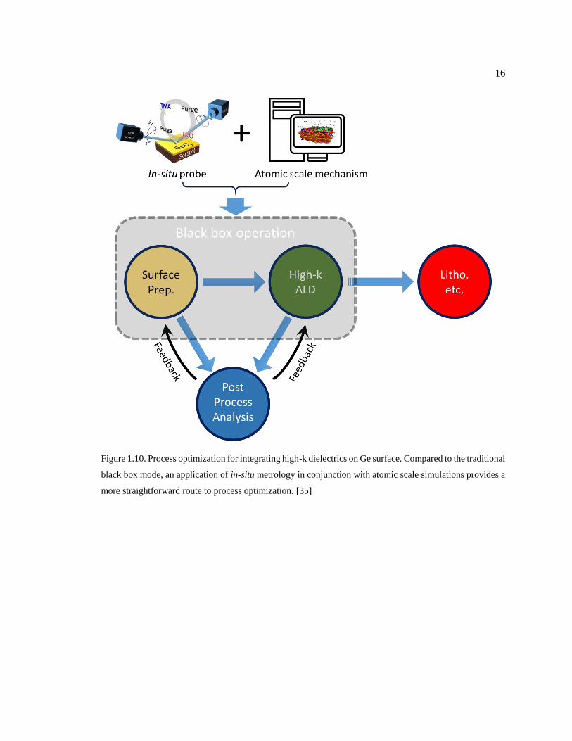
Figure 1.10. Process optimization for integrating high-k dielectrics on Ge surface.
Compared to the traditional black box mode, an application of in-situ metrology in
conjunction with atomic scale simulations provides a more straightforward route to
process optimization. [35] ................................................................................................ 16
Figure 1.11. (a) Resistivity as a function of temperature for bulk 1T-TaS2, reproduced from
Ref. [41]. Schematic views for device switching performance in (b) Boltzmann and
(c) Landau switch, respectively........................................................................................ 22
Figure 1.12. (a) Crystal structure of 1T-TaS2 at T> 850 C. The structural parameters are
from Ref. [47]. (b) Crystal reconstruction in CCDW phase (T< TC); the dash line

vii
indicates the supercell by 13𝑎×13𝑎 reconstruction; the arrow indicates the
displacement of Ta atoms with respected to the un-reconstructed phase at T> 850 C;
the corresponding shrinkage for A-B and B-C distances is 6.4 and 3.2%,
respectively. [60] .............................................................................................................. 22
Figure 1.13. STM images for (a) CCDW [48], and (b) NCCDW [61] phase of 1T-TaS2,
respectively. (c) A schematic view for phase transition from commensuratenearly
commensurateincommensurate CDW phase of 1T-TaS2 with increasing
temperature; the dark region represents David-star reconstruction, while the
reconstruction in the gray region is considerably suppressed or removed; the red arrow
represents the current flow in NCCDW. [42] .................................................................. 23
Figure 1.14. Ta3d orbital splitting by the crystal field. [50] (b) The Brillouin zone (BZ) of
1T-TaS2 at CCDW phase (T<TC); the larger BZ (solid) corresponds to the un-
reconstructed phase (T>850C), while the smaller BZ (dash) is for the supercell after
reconstruction at CCDW phase. [60] (c) Band structure of CCDW phase with
considering spin-orbital coupling for one monolayer 1T-TaS2; the band gap
EG≈0.2eV. [50] (d) Density of state (DOS) contribution from a, b, and c sites of Ta
in David-star (Fig. 2b) at CCDW phase. [50] (e) Density of state (DOS) contribution
from different Ta3d-orbitals at CCDW phase. [50] ......................................................... 24
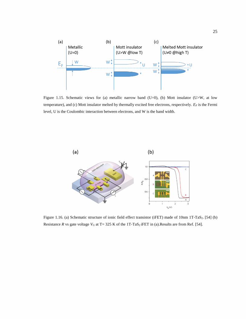
Figure 1.15. Schematic views for (a) metallic narrow band (U=0), (b) Mott insulator (U>W,
at low temperature), and (c) Mott insulator melted by thermally excited free electrons,
respectively. EF is the Fermi level, U is the Coulombic interaction between electrons,
and W is the band width. .................................................................................................. 25
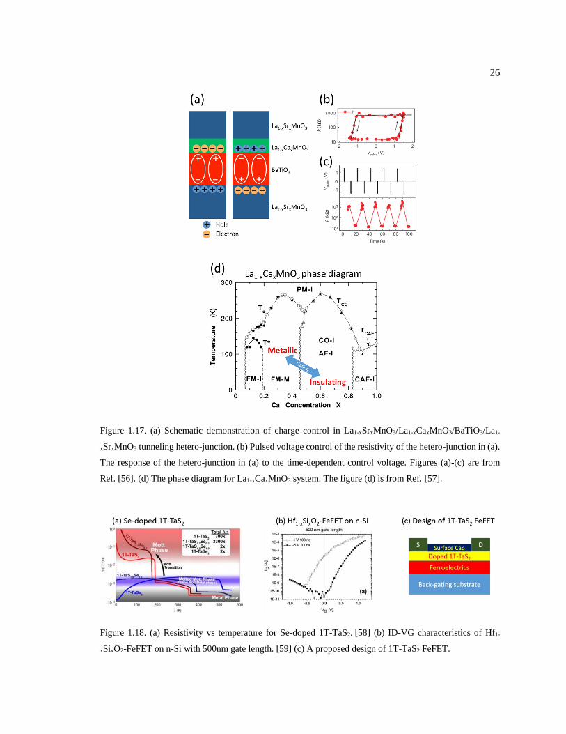
Figure 1.16. (a) Schematic structure of ionic field effect transistor (iFET) made of 10nm
1T-TaS2. [54] (b) Resistance R vs gate voltage VG at T= 325 K of the 1T-TaS2 iFET
in (a).Results are from Ref. [54]. ..................................................................................... 25
Figure 1.17. (a) Schematic demonstration of charge control in La1-xSrxMnO3/La1-
xCaxMnO3/BaTiO3/La1-xSrxMnO3 tunneling hetero-junction. (b) Pulsed voltage
control of the resistivity of the hetero-junction in (a). The response of the hetero-
junction in (a) to the time-dependent control voltage. Figures (a)-(c) are from
Ref. [56]. (d) The phase diagram for La1-xCaxMnO3 system. The figure (d) is from
Ref. [57]. .......................................................................................................................... 26
Figure 1.18. (a) Resistivity vs temperature for Se-doped 1T-TaS2. [58] (b) ID-VG
characteristics of Hf1-xSixO2-FeFET on n-Si with 500nm gate length. [59] (c) A
proposed design of 1T-TaS2 FeFET. ................................................................................ 26
Figure 1.19. Schematics of growth setup for (a) CVT, [75,76] (b) CVD, [63] (c) van der
Waals epitaxy, [77] and (d) solvothermal method. [66] .................................................. 30
Figure 1.20. (a) Schematic illustration of one growth cycle of an ALD MoS2 film on c-
sapphire. (b) SEM and AFM images for MoS2 after 800C anneal. The results are
from Ref. [78]. ................................................................................................................. 31

viii
Figure 1.21. Controlled synthesis of ultrathin 1T-TaS2 crystals via a CVD method. (a)
Schematic of CVD setup for the growth of 1T-TaS2 on a SiO2/Si substrate with
tantalum pentachloride powder and sulfur powder used as the precursors. (b, c) Crystal
structure of distorted 1T-TaS2 on a SiO2/Si substrate. (d, e) Optical images of 1T-TaS2
ultrathin flakes. (f) The controlled thicknesses of 1T-TaS2 at different growth times.
The inset shows an octahedral arrangement of the central Ta atom coordinated with S
atoms. (g−l) AFM images and their corresponding height profiles of various 1T-TaS2
at different growing times. The scale bars are 10 μm in parts d and e and 2 μm in parts
g, h, and i. These results are from Ref. [74]. .................................................................... 32
Figure 2.1. A schematic for the sequential process for growing Al2O3 by ALD using TMA
and H2O as the precursors. ............................................................................................... 38
Figure 2.2. A schematic for the ALD system of ALD-150LX. The figure was originally
plotted by Jason Lapano from Roman Engel-Herbert group at MatSE, Penn State
University. ........................................................................................................................ 40
Figure 2.3. A schematic of the home-made ALD system for synthesizing transition metal
dichalcogenides. ............................................................................................................... 42
Figure 2.4. The structure of the showerhead used in the home-made ALD system. ............... 43
Figure 2.5. The structure of the heater used in the home-made ALD system. ......................... 43
Figure 2.6. A schematic for the setup of the ellipsometry measurement. ................................ 48
Figure 2.7. Reflection and transmission of an incident light at the boundary between a
homostructure sample and air/vacuum in the SE measurement. ...................................... 48
Figure 2.8. (a) A schematic for the backside reflection of the sample and resultant
interfering signal in the SE measurement of non-absorbing substrate. (b)
Depolarization of the SE signals for single- and double-side polished Si substrates. ...... 48
Figure 2.9. Multi-reflection inside the thin film for measuring a film/substrate
heterostructure by SE. ...................................................................................................... 52
Figure 2.10. The evolution of ellipsometric angles / with respect to an increasing
thickness of SiO2 thin film (d=0~284.2 nm, n1=1.457, k1=0) on a Si substrate
(n2=3.8812, k2=0.0195). The incident light is HeNe laser with a wavelength =632.8
nm at an incident angle of 70 °. (a) /evolution as functions of the SiO2 thickness.
(b) /evolution trajectory as the SiO2 thickness increases from 0 to 284.2 nm. .......... 52
Figure 2.11. / evolution trajectory for growing of a-Si:H on a single crystal Si substrate.
The refractive index of a-Si:H is n=5-i0.85 at 500 nm. This figure is reproduces from
Ref. [97]. .......................................................................................................................... 53
Figure 2.12. Schematic for the bottom-up strategy of characterizing multi-layer structure
by SE. ............................................................................................................................... 53

ix
Figure 2.13. Dielectric function models used in ellipsometry data analysis. Figure is copied
from Ref. [97]. HOA stands for harmonic oscillator approximation, and MDF for
model dielectric function.................................................................................................. 53
Figure 2.14. Examples for the dispersion of (a) Lorentz, (b) Cauchy, and (c) Tauc-Lorentz
models used in the ellipsometry data analysis. ................................................................ 54
Figure 2.15. The optic configuration for M-2000U J.A.Woollam spectroscopic
ellipsometer. ..................................................................................................................... 56
Figure 2.16. (a) Equivalent circuit for the admittance measurement of a MOSCap device.
(b) The contributions to the capacitance from the gate oxide and semiconductor. .......... 60
Figure 2.17. Simulated band diagrams, stack capacitance Cstack, and semiconductor
capacitance Cs for (a) accumulation, (b) flat band, (c) depletion, and (d) inversion
regimes of an ideal MOSCap made of Cu(3nm)/HfO2(3nm)/p-Si (Na=3.3e17 cm-3).
The work function of Cu is m=4.5 eV, dielectric constant of HfO2 is k=25, and
dielectric constant of Si is k=11.7. The calculated Debye length is LD 7.1 nm. The
threshold voltage is Vth= 0.368 V. .................................................................................... 61
Figure 2.18. (a) The capacitance contributions for a MOSCap device with interface trap
states (Dit). Cit represents the capacitance from the interface trap states Dit. (b) Stretch-
out effect in C-V characteristics caused by the interface trap states Dit. .......................... 65
Figure 2.19. (a) Charge exchange between an interface trap state (Eit) and the majority-
carrier band (valence band for p-type semiconductor). (b) Frequency dispersion in C-
V characteristics caused by the interface trap states Dit inside the band gap. .................. 66
Figure 2.20. (a) Charge exchange between a border trap state (Nbt) and the accumulation
charge carrier (holes for a p-type semiconductor) at the semiconductor surface near
the Fermi level (EF). (b) The equivalent circuit for a MOSCap device with border trap
states; this schematic is reproduced from Ref. [104]. ...................................................... 66
Figure 2.21. (a) Hysteresis (VFB) in a bi-directional C-V measurement of MOSCap. (b)
The response of mobile oxide charge to the gate voltage modifies the electric field
inside the gate dielectric, and therefore modifies the band bending (dash). .................... 70
Figure 2.22. (a) MOSCap using metal/high-k/Si structure. The figure is released by
Intel. [108] (b) Benchmarking the band gap vs the dielectric constant for various
dielectrics. The figure is copied from Ref. [109].In particular, the band gap and
dielectric constant for GeO2 are EG=6.1 eV [110] and k~4.5. [16] .................................. 70
Figure 2.23. (a) Schematic and (b) equivalent circuit for measuring JG-V measurement of
MOSCap. (c) Example of leakage current as a function of gate voltage. ........................ 70
Figure 2.24. (a) Principles of XPS measurements: interaction between the X-ray photon
and inner core electrons. (b) An XPS survey scan for a GeO2(10 nm)/Ge sample. ......... 75
x
Figure 2.25. (a) XPS signal from a homogenous material. (b) XPS signal from a GeO2(10
nm)/Ge sample. ................................................................................................................ 78
Figure 2.26. A high resolution XPS measurement of Ge3d for a GeO2(10 nm)/Ge sample.
The take-off angle of the measurement is 90 °. ............................................................... 79
Figure 2.27. Calibrating SiO2 thickness on Si substrate using angle resolved XPS. This
figure is reproduced from Ref. [116]. .............................................................................. 79
Figure 2.28. The hardware setup for an XPS measurement. The figure is take from
Ref. [117]. ........................................................................................................................ 80
Figure 3.1. A schematic for the remote inductively coupled H2 plasma source. An induction
coil is used to generate AC electromagnetic field inside quartz tube. The flowing gas
molecules are ionized or dissociated and then react with the sample surface. ................. 85
Figure 3.2. High resolution XPS measurements of Ge 3d at a 90 ° take-off angle for
GeO2(10 nm)/Ge samples (a) before H2 plasma, (b) after H2 plasma at T=110 °C, and
(c) after H2 plasma at T=330 °C. The numerical deconvolution is based on
References [112–114] with a Tougaard background profile. A Voigt profile (0.667
branching ratio) is used to describe all the peak shapes. The Ge0 3d5/2 peak is
referenced to 29.3 eV. Binding energy shift for Ge 3d3/2 with respect to Ge 3d5/2 is
0.58eV, and the areal ratio between Ge 3d3/2 and Ge 3d5/2 is fixed at 0.67. The core
level shifts for +1, +2, +3, and +4 are 0.8,1.8,2.7,3.3 eV, respectively. .......................... 87
Figure 3.3. (a) A schematic for using a shadow mask to create a step during the H2 plasma
clean. AFM line scans across the height steps and the corresponding schematics for
the resultant structures created in the H2 plasma at (b) 110 °C and (c) 330 °C, with the
left side of the steps covered by the shadow mask. .......................................................... 90
Figure 3.4. (a) In-situ SE monitoring of H2 plasma clean of GeO2(~1 nm)/Ge(100) at 110
and 270 °C. (b) The surface morphology of Ge(100) substrate after H2 plasma clean.
(c) The surface roughening as a function of temperature. ................................................ 91
Figure 3.5. Raman measurements for GeO2(10 nm)/Ge samples (a) before H2 plasma, (b)
after H2 plasma at T=110 °C, and (c) after H2 plasma at T=330 °C. The plasma treated
samples were subsequently in-situ capped with 2 nm Al2O3 by ALD in order protect
the surface from air contamination during the sample transfer. (d) Areal percentage of
poly-Ge signal for H2-plasma treated GeO2(10 nm)/Ge samples as a function of the
process temperature. The poly-Ge percentage is normalized to the Ge bulk signal. A
linear background profile was used for the numerical deconvolution. A Voigt profile
(0.98 branching ratio) is used to describe all the peak shapes. The Ge bulk peak was
referenced to 300.9 cm-1. .................................................................................................. 94
Figure 3.6. Ellingham diagram calculation for the decomposition of GeH4. The same
calculation was also done for SiH4 as a comparison. The calculation was based on the
thermochemical data from Reference [33]. ...................................................................... 94

xi
Figure 3.7. The optimized cleaning process results in a pristine Ge surface free of oxygen,
with minimized formation of nanocrystalline Ge, atomically flat surface and a well-
defined (2×1) surface reconstruction. .............................................................................. 96
Figure 3.8. Al2O3 ALD on Al2O3(30 nm)/SiO2(25 nm)/Si. (a) In-situ SE monitoring of real-
time thickness. (b) Enlarged section for Figure (a) with details of the sequential
precursor doses, TMA adsorption and GPC. (c) Extracted ratio of GPC to TMA
adsorption as a function of growth cycle. Results published in Ref. [35]. ...................... 100
Figure 3.9. Al2O3 ALD on Ge: H surface. (a) In-situ SE monitoring of growth curve. (b)
TMA dose rise and extracted growth per cycle (GPC) as a function of ALD cycles;
the blue dash line is the base growth rate for baseline Al2O3 ALD (~0.86 Å/cycle). (c)
GPC: TMA adsorption ratio as a function of ALD cycles; the blue line is the baseline
ratio of ~0.404. AFM images for different A2lO3 ALD stages: (d) Ge: H surface before
ALD, (e) 15 ALD cycles, and (f) 27 ALD cycles, respectively. Surface roughness is
represented by root-mean-square (RMS) of height. Results published in Ref. [35]. ...... 104
Figure 3.10. Reaction profiles obtained by the ReaxFF-nudged elastic band scheme for
Al2O3 ALD on H-terminated Ge(100). (a) TMA and (b) H2O adsorptions at H-
terminated site. (c) TMA adsorption on a Ge-dangling bond. (d) H2O removes one
CH4 group from Ge-Al(CH3)2* site. (e) H2O removes CH4 group from Ge-
Al(CH3)(OH)* site. (f) TMA adsorption at Ge-Al(OH)2* site. The insets correspond
to the atomic structures for the stage at the solid points in each profile, while the
neighboring number denotes the corresponding energy. Results published in
Ref. [35]. ......................................................................................................................... 105
Figure 3.11. Results of MD simulations at 500 K for (a) 80 TMA molecules on a H-
terminated Ge(100) surface with a single Ge-dangling bond; (b) 100 H2O molecules
on the H-terminated Ge(100) surface with a Ge-Al(CH3)2* site. ReaxFF-MD results
confirm that TMA and H2O molecules preferably adsorb on the Ge-dangling and Ge-
Al(CH3)2* sites, respectively, rather than H-terminated Ge sites. Results published in
Ref. [35]. ......................................................................................................................... 106
Figure 3.12. In-situ SE monitoring for three GeOx growth modes at 270 C: (a) molecular
O2 (pO2≈33 mTorr/2min), (b) continuous O*-plasma (8 sec), and (c) sequence of O*-
plasma pulses (1.75 sec/pulse). Note the shorter time scale in (b). Results published
in Ref. [118]. .................................................................................................................... 110
Figure 3.13. (a) In-situ SE monitoring for Al2O3 ALD on GeOx(5 Å)/Ge(100). Inset is the
AFM image right after Al2O3 ALD; RMS=0.285 nm. (b) TMA dose rise and extracted
GPC as a function of ALD cycles; the ALD base GPC (blue dashi line) is ~0.86
Å/cycle. (c) Al2O3-growth/TMA-dose ratio extracted from ellipsometry; the blue line
of 0.4 is the typical value for Al2O3 ALD. (d) XPS measurements (Ge 3d at 90 ° take-
off angle) after 1 nm Al2O3 ALD on different starting surfaces, Ge: H, GeOx(3
Å)/Ge(100), and GeOx(5 Å)/Ge(100), respectively. Inset is the XPS measurements at
15 ° take-off angle. Results published in Ref. [35]. ........................................................ 111
Figure 3.14. Ellingham calculations for As2O3, GeO2, Ga2O3 and Al2O3, respectively.
Results published in Ref. [35]. ........................................................................................ 112
xii
Figure 3.15. ReaxFF-MD simulations of Al2O3 ALD using TMA+H2O dose on
GeOx(5Å)/Ge(100) surface at 1000 K. (a) Final snapshots of MD simulations for the
sequential precursor dose; the MD-NVT simulations were performed for each dose
up to 500 ps; the highlighted molecules 1 and 2 are byproducts of methane (CH4) and
ethane (H3C-CH3), respectively. (b) ReaxFF-NEB scheme for TMA adsorption on
GeOx/Ge surface. (c) Number of oxygen atoms coordinated to Ge during Al2O3 ALD.
(d) Oxygen origin of Al2O3 grown on GeOx/Ge surface after Al2O3 ALD. Results
published in Ref. [35]. ..................................................................................................... 112
Figure 3.16. ReaxFF-MD simulations for oxygen diffusion from GeOx into underlying Ge
subsurface for GeOx/Ge(100) (red) and [Al2O3/GeOx]/Ge(100) (blue) interfaces,
respectively. To accelerate the oxygen diffusion effect within a limited time frame
(2000 ps), a high temperature (800 K) was assigned to oxygen atoms, while the other
systems were kept at 300 K with the NVT-ensemble. The portion of oxygen diffusion
was normalized by the total number of oxygen atoms in GeOx layer. ............................. 113
Figure 3.17. A structural schematic for a MOSCap device using [Al2O3/GeOx] as the
interlayer between high-k and Ge. ................................................................................... 116
Figure 3.18. In-situ SE monitoring of the fabrication process: (a) H*-plasma clean of native
GeOx, (b) Ge passivation by pulsed O*-plasma, (c) Al2O3 thermal ALD, and (d) HfO2
thermal ALD, with all oxides described as Cauchy model. Results published in
Ref. [118]. ....................................................................................................................... 117
Figure 3.19. C-V characteristics of HfO2(24 Å)/Al2O3(10 Å)/GeOx/p-Ge(100) MOSCAPs
with varying GeOx thickness: (a) 0.0, (b) 2.5, and (c) 5.0 Å. (d) The effect of GeOx
thickness on MOSCAP performance. VFB is the flat-band voltage, and EV is the
valence band edge. Dit@Ev were extracted using conductance method. [169] ................ 117
Figure 3.20. C-V of HfO2(24 Å)/Al2O3/GeOx(5 Å)/p-Ge MOSCAPs with Al2O3 of (a) 0.0
Å (0 cycle), (b) 2.2 Å (4 cycles), (c) 4.9 Å (9cycles), and (d) 10.1 Å (15 cycle); (e) the
corresponding gate leakages. ........................................................................................... 118
Figure 3.21. Electrical characterization of Ni(60 nm)/HfO2(24 Å)/[Al2O3(varied
cycles)/GeOx(5 Å)]/p-Ge(100) MOSCaps. (a) Capacitance-voltage (C-V) and gate
leakage-voltage (JG-V) for the device with 9 Al2O3-ALD cycles. The Al2O3-ALD
dependence for (b) maximum capacitance (Cmax) for C-V at f=1.5 MHz, (c) gate
leakage current (JG) at over-driving V=VFB-1V (VFB is the flat-band voltage), (d) C-V
hysteresis (flat-band voltage shift, VFB), (e) interface trap density (Dit) at valence
band edge (E=EV). The Dit was obtained by analyzing frequency-dependent C-V
characteristics based on conductance method. [169] ....................................................... 118
Figure 3.22. Gate leakage (JG@VFB-1V) vs. EOT benchmark of Ge MOSCAPs using
HfO2(24 Å)/Al2O3/GeOx(5 Å) gate stacks with 0, 4, 9, and 15 cycles of ALD Al2O3
(indicated by dash arrow). EOT is calculated using [email protected] MHz. .............................. 120
Figure 4.1. The working principle of QCM for monitoring growth processes. [170] ............. 123
Figure 4.2. The cleaning process for cleaning a sapphire substrate. ........................................ 123
xiii
Figure 4.3. (a) Real-time thickness measured by in-situ QCM for ALD growth of 1T-TaS2
at low-mid temperatures (220-380 °C). (b) An enlargement for the growth at 380 °C
indicated by the black box in Figure (a). (c) 100-cycle growth represented by QCM
signals as a function of temperature. (d) Temperature dependence for QCM signal of
100 ALD cycles. .............................................................................................................. 126
Figure 4.4. A thermodynamic calculation of the ALD reaction. The critical temperature is
estimated to be 453 °C. .................................................................................................... 126
Figure 4.5. AFM measurements for TaS2 ALD growth at T=380 °C. (a) Surface
morphology at difference ALD cycles. A line scan (white dash) is shown as an inset
in each AFM image. (b) The surface coverage as a function of ALD cycle, extracted
by image processing of the AFM morphology using ImageJ software. (c) Raman
spectrum for the sample with 1000 ALD cycles. ............................................................. 127
Figure 4.6. AFM image after 500 cycles of TaCl5+ H2S ALD growth on a c-sapphire
substrate. .......................................................................................................................... 131
Figure 4.7. AFM image after 500 cycles of TaCl5+ H2S ALD growth on a Ta2O5/c-sapphire
substrate. .......................................................................................................................... 131
Figure 4.8. Raman spectrum for the sample with 500 cycles of TaCl5+H2S ALD on a
Ta2O5/sapphire substrate. ................................................................................................. 132
Figure 4.9. (a) Setup for H2S annealing the sample with 500 cycles of TaCl5+H2S ALD on
a Ta2O5/sapphire substrate. The sample photo on the left is before anneal and the one
on the right is after anneal. (b) The Raman spectrum of the sample after anneal. (c)
Raman spectrum for TaS3. [176] ...................................................................................... 132
Figure 4.10. Electric current switching of MIT transition in (a) 10 nm thick 1T-TaS2, [198]
and (b) monolayer 1T-TaS2. [178] ................................................................................... 137
Figure 4.11. Bulk carrier density of 1T-TaS2 as a function of temperature. [199] The table
on the right compares the monolayer carrier density for various materials. .................... 137
Figure 4.12. The mechanism of forming ferroelectric HfO2 at room temperature. ................. 138
Figure 4.13. The process flow for developing Al doped HfO2 ferroelectrics. ......................... 138
Figure 4.14. Characterizations of TiN sputtering. The sputtering parameters are: CMS18-
#1 sputter system in PSU Nanofab, 300Watt DC/15Watt AC, Ar:N2= 14:4.5 sccm, 5
mTorr, 3000 sec. (a) AFM measurement of the thickness step created by using a
shadow mask during the sputtering. (b) Surface morphology of sputtered TiN films
(56.23 nm) on c-plane sapphire (RMS 0.1 nm). (c) The dielectric function extracted
from spectroscopic ellipsometry, assuming a thickness of 56.23 nm. (d) XPS depth
profiling of TiN film deposited on a p+-Si substrate. ....................................................... 139
Figure 4.15. In-situ SE monitoring of 300 °C ALD growth for (a) Al2O3 calibration, (b)
HfO2 calibration, and (c) Al doped HfO2 with 1:20 cycle ratio. ...................................... 140
xiv
Figure 4.16. Process of defining electrode pattern for measuring MIM. ................................. 140
Figure 4.17. Ex-situ SE monitoring the SC1 treatment on TiN/Si samples. (a) as a
function of treatment time. (b) as a function of treatment time. (c) A schematic for
SC1 treatment. (d) at E=2.5 eV as a function of treatment time. ............................. 141
Figure 4.18. Electrical polarization as a function of electric field for MIM structures using
an insulator of (a) purge HfO2, (b) 6.6% Al doped HfO2, and (c) 12.3% Al doped
HfO2. (d) Dielectric constants for the insulators as a function of Al doping. .................. 142
xv
List of Tables
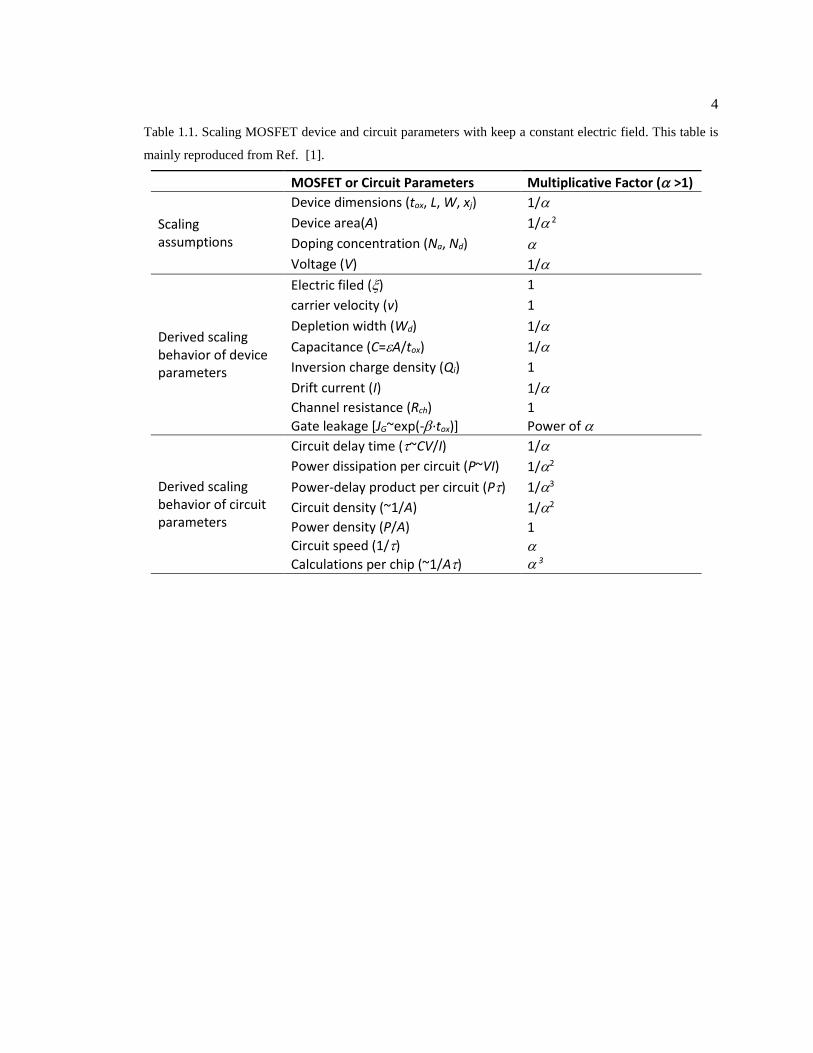
Table 1.1. Scaling MOSFET device and circuit parameters with keep a constant electric
field. This table is mainly reproduced from Ref. [1]. ...................................................... 4
Table 1.2. Basics parameters of single crystal Ge and Si. Most of the parameters are taken
from Ref. [32]. ................................................................................................................. 13
Table 2.1. Parameters for the precursors used in thermal ALD. .............................................. 39
Table 2.2. Parameters for the plasma treatments. .................................................................... 39
Table 2.3. The dielectric function of Ge substrate at T=270 °C is fitted with generalized
oscillators (Gen-Osc). inf is the contribution from the optical transitions at higher
energies, is the peak broadening, E0 is the peak transition energy, A is the transition
amplitude, and Eg is the band gap of the corresponding optical transition. ..................... 55
Table 2.4. The refractive index (n) of GeOx, Al2O3 and HfO2 deposited by ALD at T=270
°C are fitted with Cauchy model. Cn term has trivial contribution, so is not included
in the fitting. Since the band gaps of the three oxides are beyond the spectrum range
(1.24~5.18 eV), the oxides are considered as transparent with extinction coefficient
k=0. ................................................................................................................................... 55
Table 2.5. XPS parameters for Ge3d, O1s and Al2p orbitals used in this work. The calculation
of the inelastic mean free path is performed based on Ref. [115]. The XPS light source
is Al K (h= 1486.70 eV). ............................................................................................. 78
Table 2.6. Some basic properties of materials used in this work. ............................................ 78
Table 3.1. Comparison between the calculated and measured step heights created by the H2
plasma clean at 110 and 330 °C. The starting sample before the H2 plasma was using
a GeO2(10.1 nm)/Ge structure. The calculation was assuming (i) reaction mechanisms
of routes (I) and (II) for 110 and 330 °C, respectively, and (ii) 3.06 nm GeOx formation
by air oxidation on a plasma cleaned Ge surface. A density of 5.32 g/cm3 was used for
both the Ge bulk and Ge overlayer created by the H2 plasma, while 4.25 g/cm3 for
GeO2 and native GeOx formed by air exposure. .............................................................. 89
Table 3.2. De-convoluted peak areas of XPS measurements for samples after Al2O3 ALD
on Ge: H, GeOx(3 Å)/Ge(100), and GeOx(5 Å)/Ge(100), respectively. The peak area
is normalized by the area sum of Ge0 3d3/2 and Ge0 3d5/2. Results published in
Ref. [35]. ......................................................................................................................... 110
Table 4.1. Parameters for ALD growth of 1T-TaS2. ................................................................ 136
Table 4.2. Growth rates for Al2O3 and HfO2 at 300 °C. ........................................................... 136

xvi
ACKNOWLEDGEMENTS
I want to gratefully thank my advisors, Dr. Roman Engel-Herbert, and my committee
member Dr. Ari van Duin, for their diligent guidance and direction of my efforts and energy over
the years. It has been greatly fortunate to work with awesome colleagues in the lab, including Dr.
Matt Brahlek, Dr. Craig Eaton, Dr. Lei Zhang, Dr. Ryan Haislmaier, Haitian Zhang, Jason Lapano,
and Joseph Roth. Their passion for science and kind help with research have facilitated me to grow
into a researcher and engineer. Special thanks to my collaborators, Dr. G. Bruce Rayner, Jr. and
Dr. Sungwook Hong for experimental and theoretical assistance and discussions. I would like to
also thank my other friends at Penn State, Dr. Renzhong Du, Dr. Wenqing Dai, Dr. Shiming Lei,
Xiaoyu Ji, Yakun Yuan, Chenjin Zhang for all their help. Thanks to many staffs of Material
Research Institute for their experimental assistance, including Jacob Lyons, Charles Cole, Bangzhi
Liu, Bill Drawl, Tim Klinger, Andrew M. Fitzgerald, Shane P. Miller, Sarah Eichfeld, Tim Tighe,
Maria DiChol, Amanda Baker, and Jeff Long. Many thanks to the funding agents, Intermolecular
Inc. and National Science Foundation (EFRI) for making this research financially possible. Finally,
a big thank to my family, parents and brother, for their love and support.
Chapter 1
Introduction
1.1 A Brief Review of CMOS Technology
A transistor is a three-terminal semiconductor device that can regulate electronic signals
(current or voltage) and act as a switch or gate in integrated circuits (ICs). There are two basic
requirements for transistors: (i) tunability of output by a small electrical input, and (ii) saturation
of output at certain threshold input. The first transistor was the bipolar transistor invented in 1947.
A bipolar transistor utilizes a small input current to control an amplified output (see Fig. 1.1a) and
until now the bipolar circuits still remain the fastest at the individual-circuit level, but the large
power consumption has limited their application for a high-density integration (<104
circuits/chip). [1] Instead, the idea of modulating the surface conductance of the semiconductor
channel using electric field was firstly realized in 1960, by using a metal-oxide-semiconductor
field-effect transistor (MOSFET) structure (see Fig. 1.1b). In 1963, the invention of using a
complementary metal-oxide-semiconductor (CMOS) structure (see Fig. 1.1c) made possible a
negligible standby power consumption because there is always one MOS out of the pair at the OFF
state. This breakthrough soon became the foundation of the so-called “very-large-scale-integration”
(VLSI) manufacturing in semiconductor industries (see Fig. 1.2). The VLSI campaign among
semiconductor industries was mainly driven by the famous “Moore’s law”, namely, the areal
density of transistors on ICs doubled every year. In reality, the pace was slightly slow down to a
doubling rate of every 18 months. But amazingly, even after 50 years or so, this law is still working
as a guideline for the semiconductor industries (see Fig. 1.3). Beginning from 1970, the transistor
density has increased significantly from ~104/chip to >109/chip.

2
The key of keeping the Moore’s law alive for such a long time is miniaturization of the
transistor dimensions. Tab. 1.1 shows the scaling effect on MOSEFT parameters following a
constant field rule or Dennard scaling rule, in order to minimize the short channel effect when
scaling down the gate length. [1] The downscaling of transistor dimensions allows more devices
per chip operating at a faster speed, so the calculation number per chip is significantly increased.
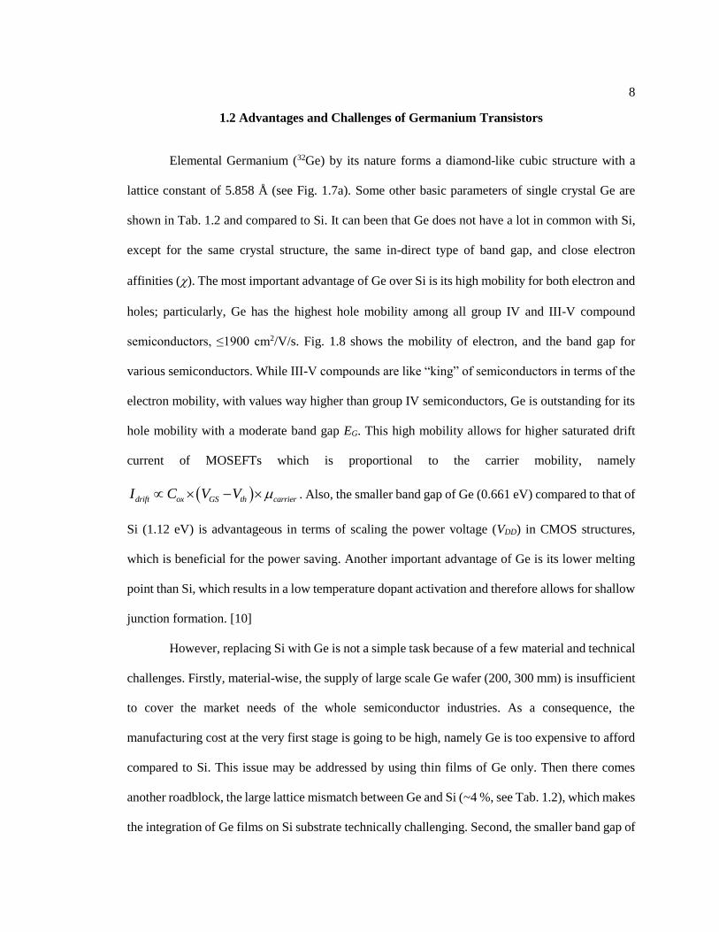
Fig. 1.4 shows the trend of technology node size. But Dennard scaling cannot keep going forever.
The first roadblock was that when scaling down the gate oxide thickness to <2 nm, which was SiO2
(dielectric constant k=3.9) in early generations of MOSEFTs, the quantum tunneling effect
becomes large, and as a result the power consumption from the leakage is ineligible and the
reliability of the device performance is compromised. To address this issue, Intel introduced
Hafnium-based high-k dielectric in junction with metallic gate and successfully produced the 45
nm node in 2008. However, as further downscaling the node size, another roadblock became
challenging, which was the leakage between drain and source caused by the drain-induced barrier
lowering (DIBL) effect in a short channel node. [1] An overcome of this technical issue requires a
better gate control of the channel. A further downscaling of gate oxide thickness even if using high-
dielectrics did not appear applicable due to the increase of gate leakage issue. Instead of
downscaling the planar transistor dimensions, in 2012, Intel firstly started using a 3D tri-gate
structure or FinFET to achieve a more effective gating and meanwhile allowing for further scaling
the node size down to ~ 7nm. Up to now, a most recent result announced by IBM in June, 2017
unveiled 5nm node with a gate-all-around FET (GAAFET) structure (see Fig. 1.5c), which is able
to squeeze ~3×10¹⁰ transistors onto a 50 mm2 sized chip!
From above, state-of-the-art technologies have been developed in the semiconductor
industries. Now the question is: what is the next? Is there still any room to move even further?
People believing in Moore’s law will generally answer: yes. But the answer is not straightforward,
because a continuing dimension scaling will eventually come to an end due to the physical limit

3
(see Fig. 1.6a). For example, in each 5 nm node, if counting the lateral dimension in Si atoms, it is
only a ~140 atom array. The device miniaturization of VLSI is now counting a handful number of
atoms. As revealed above, a useful strategy of tackling the scaling difficulty the semiconductor
industries have applied before is to introduce new materials, for example, straining Si to obtain
higher mobility channel, and substituting SiO2 with high-k dielectric to improve the gate
capacitance and suppress the gate leakage. Using the same strategy, the substitution of Si with high-
mobility semiconductors like Germanium (Ge) and III-V compound semiconductors is a promising
route to further push the development of VLSI. For example, the relatively low p-MOS Si channel
can be replaced with Ge so that the p-MOS channel mobility can pair up with that of the n-MOS
(see Fig. 1.6b). Part of this thesis will focus on Ge as the channel material of semiconductor devices,
as will be discussed later.
4
Table 1.1. Scaling MOSFET device and circuit parameters with keep a constant electric field. This table is
mainly reproduced from Ref. [1].
MOSFET or Circuit Parameters Multiplicative Factor (>1)
Scaling assumptions
Device dimensions (tox, L, W, xj) 1/
Device area(A) 1/ 2
Doping concentration (Na, Nd)
Voltage (V) 1/
Derived scaling behavior of device parameters
Electric filed () 1
carrier velocity (v) 1
Depletion width (Wd) 1/
Capacitance (C=A/tox) 1/
Inversion charge density (Qi) 1
Drift current (I) 1/
Channel resistance (Rch)
Gate leakage [JG~exp(-∙tox)]
1
Power of
Derived scaling behavior of circuit parameters
Circuit delay time (~CV/I) 1/
Power dissipation per circuit (P~VI) 1/2
Power-delay product per circuit (P) 1/3
Circuit density (~1/A) 1/2
Power density (P/A)
Circuit speed (1/)
Calculations per chip (~1/A)
1
3

5
Figure 1.1. Structural schematics for (a) NPN bipolar transistor, (b) p-MOSEFT and (c) CMOS. Figure (a) is
taken from Ref. [2].
Figure 1.2. A brief chronology of the major milestones in the semiconductor industry. The data is mainly
from Ref. [1].
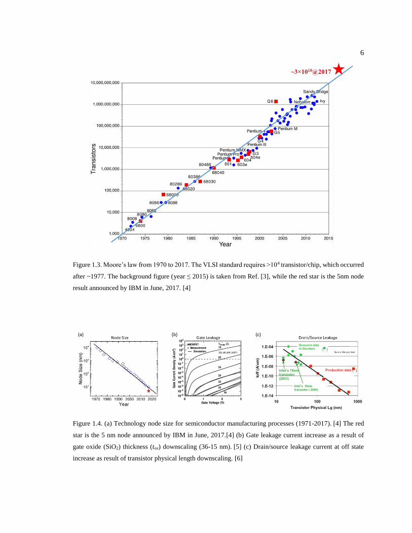
6
Figure 1.3. Moore’s law from 1970 to 2017. The VLSI standard requires >104 transistor/chip, which occurred
after ~1977. The background figure (year ≤ 2015) is taken from Ref. [3], while the red star is the 5nm node
result announced by IBM in June, 2017. [4]
Figure 1.4. (a) Technology node size for semiconductor manufacturing processes (1971-2017). [4] The red
star is the 5 nm node announced by IBM in June, 2017.[4] (b) Gate leakage current increase as a result of
gate oxide (SiO2) thickness (tox) downscaling (36-15 nm). [5] (c) Drain/source leakage current at off state
increase as result of transistor physical length downscaling. [6]

7
Figure 1.5. The structures of (a) high-k/metal gate planar MOSEFT, [7] (b) tri-gate FET, [8] and (c) gate-all-
around FET. [4]
Figure 1.6. (a) The miniaturization of transistors in VLSI is gradually approaching the physical limit. [9] (b)
Replace the low mobility Si channel in P-MOS with a high mobility semiconductor of Ge.
8
1.2 Advantages and Challenges of Germanium Transistors
Elemental Germanium (32Ge) by its nature forms a diamond-like cubic structure with a
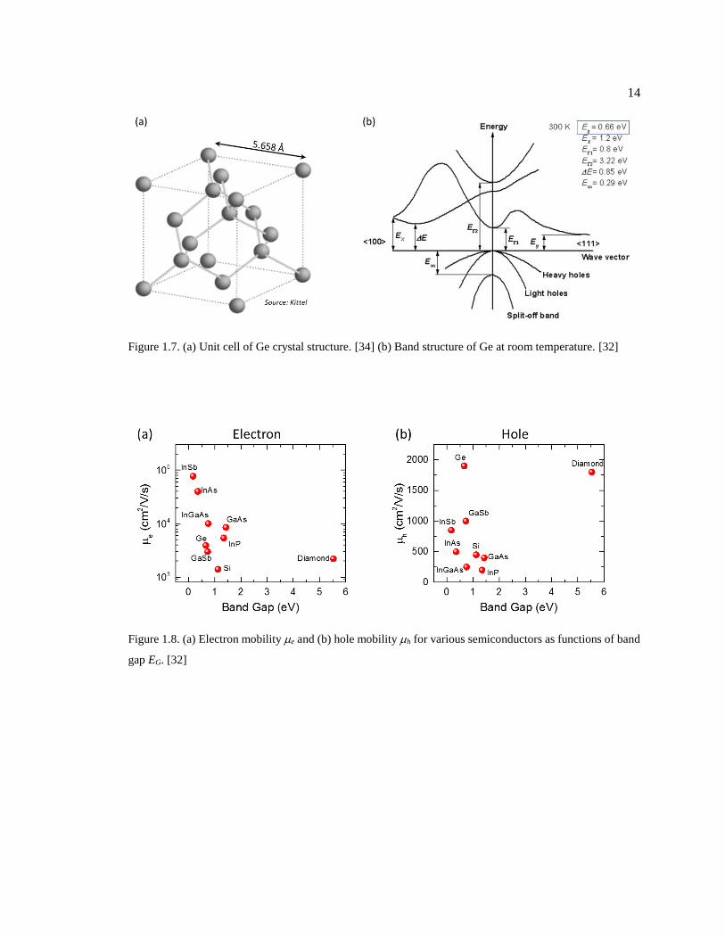
lattice constant of 5.858 Å (see Fig. 1.7a). Some other basic parameters of single crystal Ge are
shown in Tab. 1.2 and compared to Si. It can been that Ge does not have a lot in common with Si,
except for the same crystal structure, the same in-direct type of band gap, and close electron
affinities (). The most important advantage of Ge over Si is its high mobility for both electron and
holes; particularly, Ge has the highest hole mobility among all group IV and III-V compound
semiconductors, ≤1900 cm2/V/s. Fig. 1.8 shows the mobility of electron, and the band gap for
various semiconductors. While III-V compounds are like “king” of semiconductors in terms of the
electron mobility, with values way higher than group IV semiconductors, Ge is outstanding for its
hole mobility with a moderate band gap EG. This high mobility allows for higher saturated drift
current of MOSEFTs which is proportional to the carrier mobility, namely
drift ox GS th carrierI C V V . Also, the smaller band gap of Ge (0.661 eV) compared to that of
Si (1.12 eV) is advantageous in terms of scaling the power voltage (VDD) in CMOS structures,
which is beneficial for the power saving. Another important advantage of Ge is its lower melting
point than Si, which results in a low temperature dopant activation and therefore allows for shallow
junction formation. [10]
However, replacing Si with Ge is not a simple task because of a few material and technical
challenges. Firstly, material-wise, the supply of large scale Ge wafer (200, 300 mm) is insufficient
to cover the market needs of the whole semiconductor industries. As a consequence, the
manufacturing cost at the very first stage is going to be high, namely Ge is too expensive to afford
compared to Si. This issue may be addressed by using thin films of Ge only. Then there comes
another roadblock, the large lattice mismatch between Ge and Si (~4 %, see Tab. 1.2), which makes
the integration of Ge films on Si substrate technically challenging. Second, the smaller band gap of

9
Ge leads to a larger leakage current between the drain and source at the stand-by state, due to a
lower tunneling barrier height in-between. Third, the larger dielectric constant of Ge enhances the
unwanted coupling between the drain and source, which consequently results in a more prominent
short channel effect, namely a loss of turning off the channel by gating. Last but maybe the most
important, the physicochemical properties of Ge surface are distinct from that of Si, which will be
discussed in details as follows.
When the world’s first bipolar transistor was invented in 1947, it was made of Ge. But not
for long, Ge was proven not suitable for the new technologies of MOSEFT and CMOS, because
the low quality of native oxide GeO2 was not able to effectively passivate the surface states of Ge
substrate, namely making the surface states inactive in the electrical characteristics of the devices.
Fortunately, people found a thankful alternative, Si, whose native oxide SiO2 showed a far better
behavior than GeO2. Using this combination of SiO2/Si, the semiconductor industries had been
prosperous for more than 50 years. Until now, people start looking back at Ge again for its high
mobility. There is a reason why GeO2/Ge did work in the early VLSI era, which is the
thermodynamically unstable nature of the GeO2/Ge interface. Previous reports have pointed out
that right after an ozone annealing, the formed GeO2/Ge interface yielded superior electrical
characteristics. [11] However, in an oxygen-free environment at elevated temperatures of ≥ 400 °C
(for example, dopant activation process), the following reaction occurs at the interface during the
fabrication of Ge MOSFETs (also see Fig. 1.9a): [12–15]
Ge(s) + GeO2(s) 2GeO(g). Eq. 1.1
This unstable nature can be understood as a result of the relative weak bonds of Ge-Ge and Ge-O
(see Tab. 1.2), which is not an issue for the stable SiO2/Si interface. As will be discussed later in
this thesis, the volatile product of GeO will introduce electrically active defects to both the interface
and the deep dielectric bulk.
10
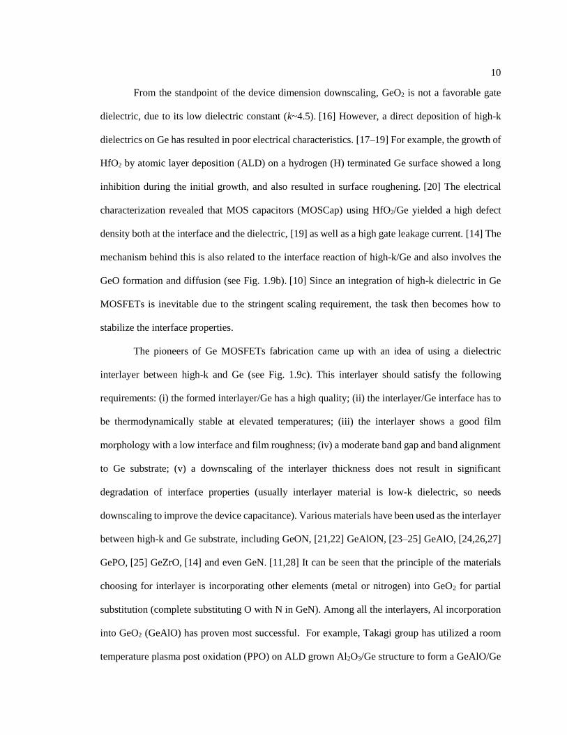
From the standpoint of the device dimension downscaling, GeO2 is not a favorable gate
dielectric, due to its low dielectric constant (k~4.5). [16] However, a direct deposition of high-k
dielectrics on Ge has resulted in poor electrical characteristics. [17–19] For example, the growth of
HfO2 by atomic layer deposition (ALD) on a hydrogen (H) terminated Ge surface showed a long
inhibition during the initial growth, and also resulted in surface roughening. [20] The electrical
characterization revealed that MOS capacitors (MOSCap) using HfO2/Ge yielded a high defect
density both at the interface and the dielectric, [19] as well as a high gate leakage current. [14] The
mechanism behind this is also related to the interface reaction of high-k/Ge and also involves the
GeO formation and diffusion (see Fig. 1.9b). [10] Since an integration of high-k dielectric in Ge
MOSFETs is inevitable due to the stringent scaling requirement, the task then becomes how to
stabilize the interface properties.
The pioneers of Ge MOSFETs fabrication came up with an idea of using a dielectric
interlayer between high-k and Ge (see Fig. 1.9c). This interlayer should satisfy the following
requirements: (i) the formed interlayer/Ge has a high quality; (ii) the interlayer/Ge interface has to
be thermodynamically stable at elevated temperatures; (iii) the interlayer shows a good film
morphology with a low interface and film roughness; (iv) a moderate band gap and band alignment
to Ge substrate; (v) a downscaling of the interlayer thickness does not result in significant
degradation of interface properties (usually interlayer material is low-k dielectric, so needs
downscaling to improve the device capacitance). Various materials have been used as the interlayer
between high-k and Ge substrate, including GeON, [21,22] GeAlON, [23–25] GeAlO, [24,26,27]
GePO, [25] GeZrO, [14] and even GeN. [11,28] It can be seen that the principle of the materials
choosing for interlayer is incorporating other elements (metal or nitrogen) into GeO2 for partial
substitution (complete substituting O with N in GeN). Among all the interlayers, Al incorporation
into GeO2 (GeAlO) has proven most successful. For example, Takagi group has utilized a room
temperature plasma post oxidation (PPO) on ALD grown Al2O3/Ge structure to form a GeAlO/Ge
11
interface. The as-formed interface shows a state-of-the-art interface quality an atomically flatness
and sharpness (see Fig. 1.9d), as well as superior electrical characteristics with a high capacitance
density, low defect state density, and low gate leakage current. [26,29]
Material-wise, the gate dielectrics used in Ge MOSFET are mainly grown by ALD because
of the high quality films grown by ALD can meet the stringent demand for the device scaling (more
details about ALD mechanism will be discussed in Chapter 2). [30,31] During the fabrication of
Ge MOSFET, the ALD process optimization is carried out mainly through a feedback loop between
the process and post-process analysis, while the process itself remains as a black box, unavailable
for a direct detection (see Fig. 1.10). The back-and-forth in this loop is simple for most of the time,
because the researchers only need to list all the process parameters and make a so-called “design
of experiments” or DOE so as to map out all the possible combinations and thereafter pick out the
one yielding the best results. However, when dealing with multiple parameters that are entangled
with each other, the roadmap to a highly scaled and electrically reliable Ge devices is not
straightforward due to a lack of in-situ probing metrology and atomic scale mechanism of the
process. Particularly in the process of high-k ALD on Ge, the growth kinetics play an important
role in determining the dielectric properties and the interface characteristics, and therefore an
understanding of the kinetics becomes crucial for improving the device performance.
In this thesis, an in-situ spectroscopic ellipsometry (SE) was used to real-time monitor the
fabrication process of Ge MOSCaps, in conjunction with ex-situ metrologies and a ReaxFF reactive
force field simulation (in collaboration with Prof. Adri van Duin group at Penn State University)
of the ALD growth kinetics. The objectives are as follows:
1) Investigate and optimize a cleaning process to in-situ prepare a pristine Ge
surface, free of oxygen and atomically flat; a pristine starting surface can exclude
the unwanted inference from the extrinsic factors;
2) Investigate the nucleation mechanism of ALD on Ge surface;
12
3) Optimize the gate dielectric stack structure on Ge and evaluate the electrical
consequences.

13
Table 1.2. Basics parameters of single crystal Ge and Si. Most of the parameters are taken from Ref. [32].
Property Si Ge
Lattice constant (Å) 5.431 5.658
Atomic density (cm-3) 5.01E+22 4.41E+22
Dielectric constant k 11.7 16
Bond length (Å) 2.3 2.41
Bond strength (kJ/mol) 222 188
Band gap EG (eV) 1.124 0.661
Direct band gap (eV) 4.200 0.800
Conduction band maximum EC or electron affinity χ (eV) 4.05 4.00
Valence band maximum EV (eV) 5.17 4.66
Intrinsic carrier concentration ni (cm-3) 1.0E+10 2.0E+13
Effective density of states (cm-3) Conduction band NC 2.9E+19 1.0E+19
Valence band NV 3.1E+19 5.0E+18
Mobility (cm2/V/s) Electron e ≤1400 ≤3900
Holeh ≤450 ≤1900
Thermal velocity vt (cm/s) Electron vt,e 2.30E+05 3.30E+05
Hole vt,h 1.65E+05 1.90E+05
Electron effective mass me (m0) Longitudinal mle 0.98 1.6
Transverse mte 0.19 0.08
Hole effective mass mh (m0) Light hole mlh 0.16 0.043
Heavy hole mhh 0.49 0.33
Melting point Tm (°C) 1415 938.2
Native oxide
Formula SiO2 GeO2
Formation energy (kJ/mol) [33]
−910.86 -579.90
Dielectric constant k [16] 3.9 4.5
14
Figure 1.7. (a) Unit cell of Ge crystal structure. [34] (b) Band structure of Ge at room temperature. [32]
Figure 1.8. (a) Electron mobility e and (b) hole mobility h for various semiconductors as functions of band
gap EG. [32]
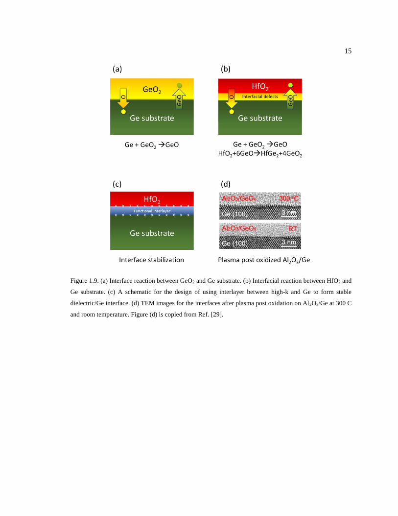
15
Figure 1.9. (a) Interface reaction between GeO2 and Ge substrate. (b) Interfacial reaction between HfO2 and
Ge substrate. (c) A schematic for the design of using interlayer between high-k and Ge to form stable
dielectric/Ge interface. (d) TEM images for the interfaces after plasma post oxidation on Al2O3/Ge at 300 C
and room temperature. Figure (d) is copied from Ref. [29].
16
Figure 1.10. Process optimization for integrating high-k dielectrics on Ge surface. Compared to the traditional
black box mode, an application of in-situ metrology in conjunction with atomic scale simulations provides a
more straightforward route to process optimization. [35]
17
1.3 Properties of 2D Layered Material 1T-TaS2
The recently developed exfoliation method has re-triggered the research interests on mono-
layer 2-dimensional layered materials (2DLM) or van der Waals (vdW) materials. [36] 2DLMs
have demonstrated diverse fundamental physics, ranging from conductors (e.g. graphene [37]),
semiconductors (e.g. transition metal dichalcogenide (TMD) [38]), wide band-gap insulators (e.g.
hexagonal Boron Nitride (hBN) [39]), and superconductors (e.g. Niobium Selenide (NbSe2) [40]).
Among all, layered Tantalum disulfide (1T-TaS2) has been particularly attractive due to its unique
and strong electron-correlation which results in a metal-to-insulator transition (MIT). As shown in
Fig.1.11a, an abrupt change of resistivity (~10×) occurs across the MIT transition (Tc≈ 200 K). [41]
It has been proven that this phase transition can be tuned not only by temperature, but also
pressure [42], chemical doping [43], and disorders by electron irradiation. [44] A more important
implication is that a reversible electric-field control of this correlation phenomenon makes possible
a new switch type, Landau switch. In traditional Boltzmann switch using group IV and III-V
compound semiconductor as the channel (see Fig. 1.11b), there is a fundamental physical limit,
which is the switching slope > ln(10)kBT/q= 60 mV/dec. The abrupt transport change during the
MIT transition potentially provides a solution to this physical limitation, with a much faster
switching swing (see Fig. 1.11c). [45] This switching mechanism is plausible in layered 1T-TaS2
because: (i) the electron-electron correlation is stronger than the electron-lattice interaction
(Ueff/W=1.5>1.3) [46], (ii) the nanoscale thickness of the materials makes possible a field-effect
control even in correlated systems, whereas the high electron density (~1021 cm-3) suppresses the
screening length down to ~nm. [45]
TaS2 has a few polymorphs, including 1T-, 2H-, 3R- and 6R-TaS2, all of which are vdW
materials. [47] The prefix for each structure represents a short description of the structure; taking
1T-TaS2 for example, ‘1’ means the stacking period along c-direction is one TaS2 slab, and ‘T’
18
represents ‘trigonal’; in other cases, ‘H’ is ‘hexagonal’, and ‘R’ is ‘rhombohedral’. Among all these
polymorphs, only 1T-TaS2 shows a MIT transition, and therefore becomes the material of interest
in our research. The parental crystal structure of 1T-TaS2 is a Cd(OH)2 type (space group= 𝑃3̅𝑚1)
at elevated temperatures (T> 850 C), as shown in Fig. 1.12a; in the slab plane, each Ta (green) is
six-fold coordinated by S atoms (yellow), equally locating on the top of and underneath Ta sub-
layer, while each S coordinates to three Ta atoms; in-between the slabs, there is no strong bonding,
or nearly van der Waals bonding. The low temperature phases are basically a distortion of this
parental structure. At Mott insulator state (T< TC≈ 200 K), a commensurate charge density wave
(CCDW) is developed. [42] To accommodate this charge localization, the lattice reconstructs by
forming a David-star pattern, with 12 Ta atoms at the star corners displaced toward the center Ta
(Fig. 1.12b), as revealed by previous scan tunneling microscopy (STM) (Fig. 1.13a) [48]; as a
consequence, a √13𝑎×√13𝑎×13𝑐 supercell is derived. [49] At medium temperatures (TC< T< 350
K), the CDW phase is partially melted, whereas the David-star pattern is sustained locally in a
domain form (Fig. 1.13b), i.e. a nearly commensurate charge density wave (NCDW). The gray
region developed in-between domains (Fig. 1.13c) forms conducting channels for electrons, and
therefore results in a significant reduction of resistivity, as mentioned above (Fig. 1a). At even
higher temperatures (T> 350 C), the David-star pattern completely disappears (Fig. 1.13c), and is
replaced by an incommensurate charge density wave (ICDW), leaving a pure metallic phase.
The above-mentioned MIT transition in 1T-TaS2 originates from the strong electron-
electron correlation. The system Hamiltonian is typically described by a Hubbard model [42]:
, , ,
. .i j ii ii j i i
H t c c h c U n n n
. Eq. 1.2
i jc c
is the creation (annihilation) operator of single electron on ith site with spin,
i i in c c
is the corresponding electron number operator, t is the electron wavefunction overlap
or hopping integral between the neighboring sites, U is the Coulombic interaction between
19
electrons, and is the chemical potential. Tight-binding calculation shows that at CCDW phase,
the David-star reconstruction leads to a gapping of the twelve Ta3d electrons from the Ta atoms at
the David-star outer-shell (Fig. 1.14d), i.e. B and C sites in Fig. 1.12b; the thirteenth electron from
the center Ta atom (a site) form a narrow band (band with W≈80 meV) around EF. [50] This narrow-
band feature is typical in d orbitals of transition metal, whereas the neighboring hopping t is small
in Eq. 1.2; when the hopping term t is comparable to the Coulombic interaction U, a MIT transition
may occur. [51] The physical picture of Mott insulator state can be understood as Fig. 1.15. [45]
Without the electron-electron interaction U, the narrow band is half-filled, forming a metallic state
(Fig. 1.15a). The electron-electron interaction U breaks the degeneracy in the narrow band, and
therefore split it into two sub-bands, upper and lower Hubbard bands (UHB and LHB), as shown
in Fig. 1.15b; with LHB fully occupied, the system undergoes a Mott-Hubbard transition, leading
to a high resistivity. A transition between the metallic and insulating states requires a tuning of U/t
ratio [51], by either tuning U or t alone or both. [42] For example, an elevated temperature results
in more free electrons by thermal excitation, and results in a screening of the Coulombic interaction
U [52], i.e. a reduction of effective U. So beyond certain temperature, the UHB bottom would meet
with LHB top, and they merge into one band as a whole (Fig. 1.15c). The criterion for melting Mott
insulating phase is also pointed out by Mott [52]:
1/3 0.25c Hn a . Eq. 1.3
nc is the critical free electron density, and aH is an effective Bohr radius of the isolated (localized-
electron) center. Bohr radius aH is usually described as [52,53]:
2
* 2
4Ha
m e
. Eq. 1.4
is the background dielectric constant, and m* is the effective mass of electrons in the conduction
band.
20
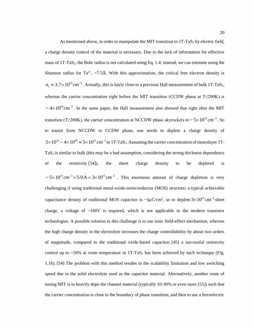
As mentioned above, in order to manipulate the MIT transition in 1T-TaS2 by electric field,
a charge density control of the material is necessary. Due to the lack of information for effective
mass of 1T-TaS2, the Bohr radius is not calculated using Eq. 1.4; instead, we can estimate using the
Shannon radius for Ta4+, ~7.5Å. With this approximation, the critical free electron density is
19 33.7 10cn cm . Actually, this is fairly close to a previous Hall measurement of bulk 1T-TaS2,
whereas the carrier concentration right before the MIT transition (CCDW phase at T≤200K) is
19 3~ 4 10 cm . In the same paper, the Hall measurement also showed that right after the MIT
transition (T≥200K), the carrier concentration at NCCDW phase skyrockets to21 3~ 5 10 cm . So
to transit from NCCDW to CCDW phase, one needs to deplete a charge density of
21 19 21 35 10 4 10 5 10 cm in 1T-TaS2. Assuming the carrier concentration of monolayer 1T-
TaS2 is similar to bulk (this may be a bad assumption, considering the strong thickness dependence
of the resistivity [54]), the sheet charge density to be depleted is
21 3 15 2~ 5 10 5.9A 3 10cm cm . This enormous amount of charge depletion is very
challenging if using traditional metal-oxide-semiconductor (MOS) structure; a typical achievable
capacitance density of traditional MOS capacitor is ~3C/cm2, so to deplete15 23 10 cm sheet
charge, a voltage of ~160V is required, which is not applicable in the modern transistor
technologies. A possible solution to this challenge is to use ionic field-effect mechanism, whereas
the high charge density in the electrolyte increases the charge controllability by about two orders
of magnitude, compared to the traditional oxide-based capacitor; [45] a successful resistivity
control up to ~50% at room temperature in 1T-TaS2 has been achieved by such technique (Fig.
1.16). [54] The problem with this method resides in the scalability limitation and low switching
speed due to the solid electrolyte used as the capacitor material. Alternatively, another route of
tuning MIT is to heavily dope the channel material (typically 10-30% or even more [55]) such that
the carrier concentration is close to the boundary of phase transition, and then to use a ferroelectric
21
(FE) capacitor material to gate the channel; note that a typical achievable capacitance density of
FE material like Pb(Zr,Ti)O3 (PZT) is about 30C/cm2, one order of magnitude higher than
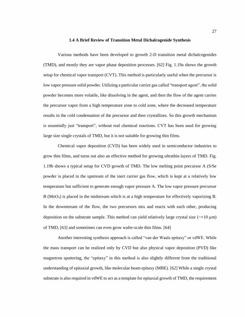
traditional gate oxide. This strategy has been successful in La1-xSrxMnO3/La1-
xCaxMnO3/BaTiO3/La1-xSrxMnO3 hetero-junctions (Fig. 1.17a-c), [56] whereas La1-xCaxMnO3 is
the functional MIT material whose conductance can be tuned by electric gating. [57] Analogous to
this, a ferroelectric field effect transistor (FeFET) based on doped 1T-TaS2 is plausible: (i) its MIT
transition is susceptible to chemical doping, and can be even strongly suppressed (e.g. Se-doped
1T-TaS2 in Fig. 1.18a [58]); (ii) a simple atomic-layer-deposition (ALD) method can be applied in
the integration of ferroelectric materials (e.g. Si FeFET in Fig. 1.18b [59]), so that the fabrication
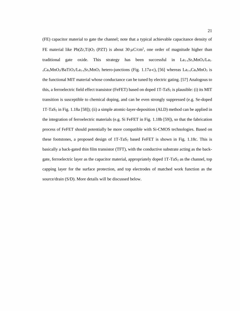
process of FeFET should potentially be more compatible with Si-CMOS technologies. Based on
these footstones, a proposed design of 1T-TaS2 based FeFET is shown in Fig. 1.18c. This is
basically a back-gated thin film transistor (TFT), with the conductive substrate acting as the back-
gate, ferroelectric layer as the capacitor material, appropriately doped 1T-TaS2 as the channel, top
capping layer for the surface protection, and top electrodes of matched work function as the
source/drain (S/D). More details will be discussed below.
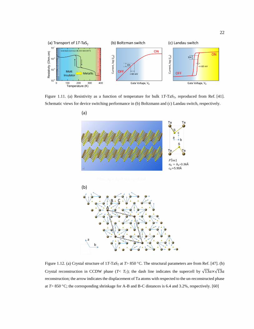
22
Figure 1.11. (a) Resistivity as a function of temperature for bulk 1T-TaS2, reproduced from Ref. [41].
Schematic views for device switching performance in (b) Boltzmann and (c) Landau switch, respectively.
Figure 1.12. (a) Crystal structure of 1T-TaS2 at T> 850 C. The structural parameters are from Ref. [47]. (b)
Crystal reconstruction in CCDW phase (T< TC); the dash line indicates the supercell by √13𝑎×√13𝑎
reconstruction; the arrow indicates the displacement of Ta atoms with respected to the un-reconstructed phase
at T> 850 C; the corresponding shrinkage for A-B and B-C distances is 6.4 and 3.2%, respectively. [60]
23
Figure 1.13. STM images for (a) CCDW [48], and (b) NCCDW [61] phase of 1T-TaS2, respectively. (c) A
schematic view for phase transition from commensuratenearly commensurateincommensurate CDW
phase of 1T-TaS2 with increasing temperature; the dark region represents David-star reconstruction, while
the reconstruction in the gray region is considerably suppressed or removed; the red arrow represents the
current flow in NCCDW. [42]

24
Figure 1.14. Ta3d orbital splitting by the crystal field. [50] (b) The Brillouin zone (BZ) of 1T-TaS2 at CCDW
phase (T<TC); the larger BZ (solid) corresponds to the un-reconstructed phase (T>850C), while the smaller
BZ (dash) is for the supercell after reconstruction at CCDW phase. [60] (c) Band structure of CCDW phase
with considering spin-orbital coupling for one monolayer 1T-TaS2; the band gap EG≈0.2eV. [50] (d) Density
of state (DOS) contribution from a, b, and c sites of Ta in David-star (Fig. 2b) at CCDW phase. [50] (e)
Density of state (DOS) contribution from different Ta3d-orbitals at CCDW phase. [50]
25
Figure 1.15. Schematic views for (a) metallic narrow band (U=0), (b) Mott insulator (U>W, at low
temperature), and (c) Mott insulator melted by thermally excited free electrons, respectively. EF is the Fermi
level, U is the Coulombic interaction between electrons, and W is the band width.
Figure 1.16. (a) Schematic structure of ionic field effect transistor (iFET) made of 10nm 1T-TaS2. [54] (b)
Resistance R vs gate voltage VG at T= 325 K of the 1T-TaS2 iFET in (a).Results are from Ref. [54].
26
Figure 1.17. (a) Schematic demonstration of charge control in La1-xSrxMnO3/La1-xCaxMnO3/BaTiO3/La1-
xSrxMnO3 tunneling hetero-junction. (b) Pulsed voltage control of the resistivity of the hetero-junction in (a).
The response of the hetero-junction in (a) to the time-dependent control voltage. Figures (a)-(c) are from
Ref. [56]. (d) The phase diagram for La1-xCaxMnO3 system. The figure (d) is from Ref. [57].
Figure 1.18. (a) Resistivity vs temperature for Se-doped 1T-TaS2. [58] (b) ID-VG characteristics of Hf1-
xSixO2-FeFET on n-Si with 500nm gate length. [59] (c) A proposed design of 1T-TaS2 FeFET.
27
1.4 A Brief Review of Transition Metal Dichalcogenide Synthesis
Various methods have been developed to growth 2-D transition metal dichalcogenides
(TMD), and mostly they are vapor phase deposition processes. [62] Fig. 1.19a shows the growth
setup for chemical vapor transport (CVT). This method is particularly useful when the precursor is
low vapor pressure solid powder. Utilizing a particular carrier gas called “transport agent”, the solid
powder becomes more volatile, like dissolving in the agent, and then the flow of the agent carries
the precursor vapor from a high temperature zone to cold zone, where the decreased temperature
results in the cold condensation of the precursor and then crystallizes. So this growth mechanism
is essentially just “transport”, without real chemical reactions. CVT has been used for growing
large size single crystals of TMD, but it is not suitable for growing thin films.
Chemical vapor deposition (CVD) has been widely used in semiconductor industries to
grow thin films, and turns out also an effective method for growing ultrathin layers of TMD. Fig.
1.19b shows a typical setup for CVD growth of TMD. The low melting point precursor A (S/Se
powder is placed in the upstream of the inert carrier gas flow, which is kept at a relatively low
temperature but sufficient to generate enough vapor pressure A. The low vapor pressure precursor
B (MoO3) is placed in the midstream which is at a high temperature for effectively vaporizing B.
In the downstream of the flow, the two precursors mix and reacts with each other, producing
deposition on the substrate sample. This method can yield relatively large crystal size (~×10 m)
of TMD, [63] and sometimes can even grow wafer-scale thin films. [64]
Another interesting synthesis approach is called “van der Waals epitaxy” or vdWE. While
the mass transport can be realized only by CVD but also physical vapor deposition (PVD) like
magnetron sputtering, the “epitaxy” in this method is also slightly different from the traditional
understanding of epitaxial growth, like molecular beam epitaxy (MBE). [62] While a single crystal
substrate is also required in vdWE to act as a template for epitaxial growth of TMD, the requirement

28
of lattice mismatch is much more tolerant due to the weak van der Waals coupling between the film
and substrate. [65] This approach allows for a directional growth of TMD materials, namely the as
grown TMD flakes show a highly oriented crystal alignment.
Solution phase synthesis has also been used to grow TMD nanocrystals. For example, a
solvothermal method, which is similar to the hydrothermal synthesis, has been used to grow InSe
(see Fig. 1.19d). [66] In this method, a N2 gas was used as the reaction solvent for precursors at
elevated temperatures. The high pressure and high temperature environment inside the reactor
facilitates the reaction process. This approach is suitable for producing nanowires and nanosheets,
but not appropriate for growing ultrathin layers of TMD due to the lack of thickness control.
Atomic layer deposition (ALD) is well-known for precise control of deposition thickness,
so can be used for growing ultrathin layers of TMD materials. Fig. 1.20a shows the ALD growth
for MoS2 using MoCl5 and H2S as precursors. The self-limiting nature of ALD growth allows for a
precise thickness control from one to multiple monolayers by counting the growth cycles. More
importantly, the high conformity of ALD growth provides a large scale deposition for 2DLM
materials. However, one issue with ALD growth of TMD is that the resultant thin films are usually
amorphous due to the relatively low growth temperature, so a post-deposition annealing at high
temperature is necessary to crystallize the grown films (see Fig. 1.20b).
As for preparing ultrathin layers of 1T-TaS2, the primary method used by researchers is
still mechanical exfoliation using Scotch tape from a single crystal bulk, [54,67–70] which is grown
by a CVT method. [67,71–73] This method is simple and the as obtained flakes (< 20 m) show a
low density of defects since they are extracted directly from the fresh bulk 1T-TaS2 surface. But
the problem is that one can barely control the thickness and the shape of the flakes, which is not
favorable for the application in device manufacturing. The thickness control of 1T-TaS2 is
particularly important, because previous results have revealed that its electrical properties is
sensitive to the thickness, with a critical thickness ~ 10 nm, corresponding to ~13 monolayer, which
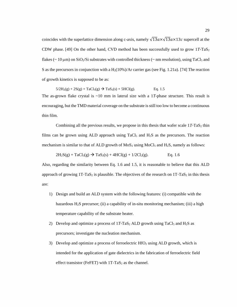
29
coincides with the superlattice dimension along c-axis, namely √13𝑎×√13𝑎×13𝑐 supercell at the
CDW phase. [49] On the other hand, CVD method has been successfully used to grow 1T-TaS2
flakes (~ 10 m) on SiO2/Si substrates with controlled thickness (~ nm resolution), using TaCl5 and
S as the precursors in conjunction with a H2(10%)/Ar carrier gas (see Fig. 1.21a). [74] The reaction
of growth kinetics is supposed to be as:
5/2H2(g) + 2S(g) + TaCl5(g) TaS2(s) + 5HCl(g). Eq. 1.5
The as-grown flake crystal is ~10 mm in lateral size with a 1T-phase structure. This result is
encouraging, but the TMD material coverage on the substrate is still too low to become a continuous
thin film.
Combining all the previous results, we propose in this thesis that wafer scale 1T-TaS2 thin
films can be grown using ALD approach using TaCl5 and H2S as the precursors. The reaction
mechanism is similar to that of ALD growth of MoS2 using MoCl5 and H2S, namely as follows:
2H2S(g) + TaCl5(g) TaS2(s) + 4HCl(g) + 1/2Cl2(g). Eq. 1.6
Also, regarding the similarity between Eq. 1.6 and 1.5, it is reasonable to believe that this ALD
approach of growing 1T-TaS2 is plausible. The objectives of the research on 1T-TaS2 in this thesis
are:
1) Design and build an ALD system with the following features: (i) compatible with the
hazardous H2S precursor; (ii) a capability of in-situ monitoring mechanism; (iii) a high
temperature capability of the substrate heater.
2) Develop and optimize a process of 1T-TaS2 ALD growth using TaCl5 and H2S as
precursors; investigate the nucleation mechanism.
3) Develop and optimize a process of ferroelectric HfO2 using ALD growth, which is
intended for the application of gate dielectrics in the fabrication of ferroelectric field
effect transistor (FeFET) with 1T-TaS2 as the channel.
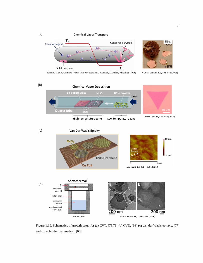
30
Figure 1.19. Schematics of growth setup for (a) CVT, [75,76] (b) CVD, [63] (c) van der Waals epitaxy, [77]
and (d) solvothermal method. [66]
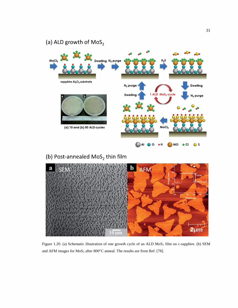
31
Figure 1.20. (a) Schematic illustration of one growth cycle of an ALD MoS2 film on c-sapphire. (b) SEM
and AFM images for MoS2 after 800C anneal. The results are from Ref. [78].

32
Figure 1.21. Controlled synthesis of ultrathin 1T-TaS2 crystals via a CVD method. (a) Schematic of CVD
setup for the growth of 1T-TaS2 on a SiO2/Si substrate with tantalum pentachloride powder and sulfur powder
used as the precursors. (b, c) Crystal structure of distorted 1T-TaS2 on a SiO2/Si substrate. (d, e) Optical
images of 1T-TaS2 ultrathin flakes. (f) The controlled thicknesses of 1T-TaS2 at different growth times. The
inset shows an octahedral arrangement of the central Ta atom coordinated with S atoms. (g−l) AFM images
and their corresponding height profiles of various 1T-TaS2 at different growing times. The scale bars are 10
μm in parts d and e and 2 μm in parts g, h, and i. These results are from Ref. [74].
33
1.5 Thesis Organization
This thesis is organized in the following chapters involving experimental techniques used
in this thesis, ALD of high-k dielectrics on Ge, ALD synthesis of 1T-TaS2 and ALD synthesis of
ferroelectric HfO2.
Chapter 2 Various key experimental techniques will be discussed in details,
including the working principle, hardware information, and data analysis. The techniques that will
be discussed are: atomic layer deposition (ALD), spectroscopic ellipsometry (SE), admittance
characterization, and X-ray photoelectron spectroscopy (XPS). Other experimental techniques like
atomic force microscopy (AFM) and Raman spectroscopy will not be discussed in details, but the
experimental parameters will be included when the corresponding data are discussed.
Chapter 3 In this chapter, a cleaning mechanism of removing native GeOx on Ge by
H2 plasma will be firstly addressed in details. It will be shown that the process temperature plays
an important role to obtain pristine Ge surfaces. Then, the nucleation mechanism of Al2O3 on two
different Ge surfaces (H-terminated and oxidized) are studied by in-situ spectroscopic ellipsometry
and ex-situ characterizations. The experimental results are compared with the ReaxFF simulations
from the collaborators (Prof. Adri van Duin group at Penn State University) to establish a structure-
property relationship so as to figure out the atomic scale mechanism. Finally, with the
understanding of the ALD mechanism on Ge, a tri-layer gate dielectric stack is proposed and
optimized to form Ge MOSCap devices. The dielectric/Ge interface qualities are evaluated by using
admittance characterizations.
Chapter 2
Experimental Techniques
This chapter will discuss about the principles of the primary experimental techniques used
in the research of this thesis, including atomic layer deposition, spectroscopic ellipsometry,
admittance measurement, and X-ray photoelectron spectroscopy. Other experimental techniques
are also used, but will only be introduced together the corresponding results.
2.1 Atomic Layer Deposition
Atomic layer deposition (ALD) technology was originally discovered developed
independently with two different names: “molecular layering” in the Soviet Union during 1960s,
and much better known as “atomic layer epitaxy (ALE)” as early as 1974 in Finland. [31,79,80] A
good reading source about the history of ALD evolution is a volunteer-based effort called virtual
project on the history of ALD (VPHA) launched in 2013. Ever since the discovery of ALE, the
technique has been further optimized and matured into an advanced deposition technology that is
widely used in semiconductor industries, particularly growing high-permittivity (high-k) dielectrics
for the gate insulators in the metal-oxide-semiconductor field effect transistor (MOSFET)
structures and for copper diffusion barriers in backend interconnects. [31,81] The self-limiting
reaction mechanism enables an atomic level control of deposition thickness by ALD, which has
significantly boosted the miniaturization of the device dimensions. More importantly, the high
conformality of ALD-grown films allows the application in depositions on high-aspect ratio
structures, e.g. a 3D structure of FinFET transistors. This advantageous feature is not achievable in
other high vacuum deposition techniques like molecular beam epitaxy (MBE) and thermal/e-beam

35
evaporation, wherein the mass transport of materials is a line-of-sight mode and therefore highly
directional. Also, the relatively low temperature required for ALD growth results in continuous,
amorphous and pin-hole-free materials in a wafer scale, which are necessary for the semiconductor
devices. Last but not the least, the low temperature is beneficial to the industry manufacturing in
terms of saving energy cost.
2.1.1 Principles of Atomic Layer Deposition
ALD growth is a surface reaction process by sequentially dosing different reactants and
separating the doses with sufficient purging. Even if using the same precursors, ALD is distinct to
chemical vapor deposition (CVD), wherein all the reacting precursors are dose simultaneously and
the reaction is driven by the high temperature near the surface in a gas phase mode. CVD is known
for fast growth, but not for a good control of thickness, surface roughness or material continuity.
The working principles of ALD is usually demonstrated by using Al2O3 growth with tri-
methyl-aluminum [Al(CH3)3, TMA] and water (H2O) precursors as an example. This reaction has
been comprehensive studied both experimentally [35,82–84] and theoretically, [35,85,86] because
Al2O3 has been extensively used as a high quality gate dielectric with a low leakage current and
relatively high permittivity, [87] as well as a high temperature and highly corrosion resistant
coating. [88] A well accepted scenario for a reaction cycle of Al2O3 ALD is shown in Fig. 2.1. A
good starting surface for Al2O3 ALD is terminated with hydroxyl groups, i.e. -OH*, where the
asterisk superscription denotes surface species. TMA molecules are transported together by inert
carrier gas (like N2, Ar) and dosed into the system and react with the –OH* groups by exchanging
one methyl group (-CH3) in TMA with the H atom in –OH*, and subsequently forming CH4
byproduct, as follows:
-OH* + Al(CH3)3 -O-Al(CH3)2* + CH4. Eq. 2.1

36
In this scenario, the reaction only occurs on the surface sites with –OH* groups, and the resultant
surface is decorated with di-methyl-aluminum (DMA) groups, namely -Al(CH3)2*. A complete
reaction requires a sufficient amount of TMA and certain time for the precursor to uniformly
distribute across the whole sample. The actual consumption of TMA is way less than the required
dosage, due to the low sticking coefficient of TMA (~10-3-10-4). [84] On the other hand, an over
dose of TMA molecules will not result in further surface reactions, because TMA is chemically
unreactive to DMA. So the chemical reaction is limited to at most one monolayer on the surface,
which is well-known as a self-limiting effect. The next step is to purge the system with inert gas to
remove the CH4 byproduct as well as the unreacted gas phase TMA molecules and any possible
physisorption of TMA on the surface, so that there will be no direct intermixing and reaction
between TMA gas and the subsequently dosed oxidant precursor H2O. The unwanted gas phase
reaction between TMA and H2O is called parasitic CVD growth, and can cause formation of Al2O3
nanoparticles above the sample surface. The nanoparticles will fall onto the surface, namely
“dusting”, and become local nucleation centers for ALD growth, so consequently the deposition
becomes non-uniform and ends up with a rough surface. A sufficient purging step in ALD growth
is of great importance to obtain high quality thin films. After completely purging TMA, the H2O
molecules are dosed to oxidize the surface DMA. H2O is highly reactive to DMA, by exchanging
its –OH with –CH3* groups in DMA and forming volatile CH4 as follows:
-O-Al(CH3)2* + 2H2O -O-Al(OH)2
* + 2CH4. Eq. 2.2
The purging step for H2O is usually longer than that for TMA, due to the stronger H2O
physisorption onto a –OH* terminated surface. Also, to insure a complete purge, an elevated
temperature is preferred (≥110 °C) to increase the desorption rate of surface H2O. From Eq. 2.1.2,
after purging H2O, the surface ends up with –OH* termination again, and is ready for the next ALD
cycle. By combining Eq. 2.1.1 and 2.1.2, the overall reaction for Al2O3 ALD is:
2Al(CH3)3 +3H2O Al2O3 + 3CH4, H= -376 kcal. [31] Eq. 2.3
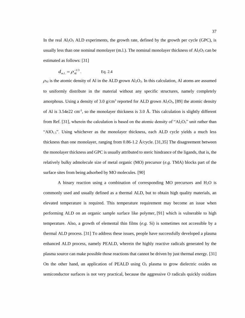
37
In the real Al2O3 ALD experiments, the growth rate, defined by the growth per cycle (GPC), is
usually less than one nominal monolayer (m.l.). The nominal monolayer thickness of Al2O3 can be
estimated as follows: [31]
1/3
. .m l Ald . Eq. 2.4
Al is the atomic density of Al in the ALD grown Al2O3. In this calculation, Al atoms are assumed
to uniformly distribute in the material without any specific structures, namely completely
amorphous. Using a density of 3.0 g/cm3 reported for ALD grown Al2O3, [89] the atomic density
of Al is 3.54e22 cm-3, so the monolayer thickness is 3.0 Å. This calculation is slightly different
from Ref. [31], wherein the calculation is based on the atomic density of “Al2O3” unit rather than
“AlO1.5”. Using whichever as the monolayer thickness, each ALD cycle yields a much less
thickness than one monolayer, ranging from 0.86-1.2 Å/cycle. [31,35] The disagreement between
the monolayer thickness and GPC is usually attributed to steric hindrance of the ligands, that is, the
relatively bulky admolecule size of metal organic (MO) precursor (e.g. TMA) blocks part of the
surface sites from being adsorbed by MO molecules. [90]
A binary reaction using a combination of corresponding MO precursors and H2O is
commonly used and usually defined as a thermal ALD, but to obtain high quality materials, an
elevated temperature is required. This temperature requirement may become an issue when
performing ALD on an organic sample surface like polymer, [91] which is vulnerable to high
temperature. Also, a growth of elemental thin films (e.g. Si) is sometimes not accessible by a
thermal ALD process. [31] To address these issues, people have successfully developed a plasma
enhanced ALD process, namely PEALD, wherein the highly reactive radicals generated by the
plasma source can make possible those reactions that cannot be driven by just thermal energy. [31]
On the other hand, an application of PEALD using O2 plasma to grow dielectric oxides on
semiconductor surfaces is not very practical, because the aggressive O radicals quickly oxidizes
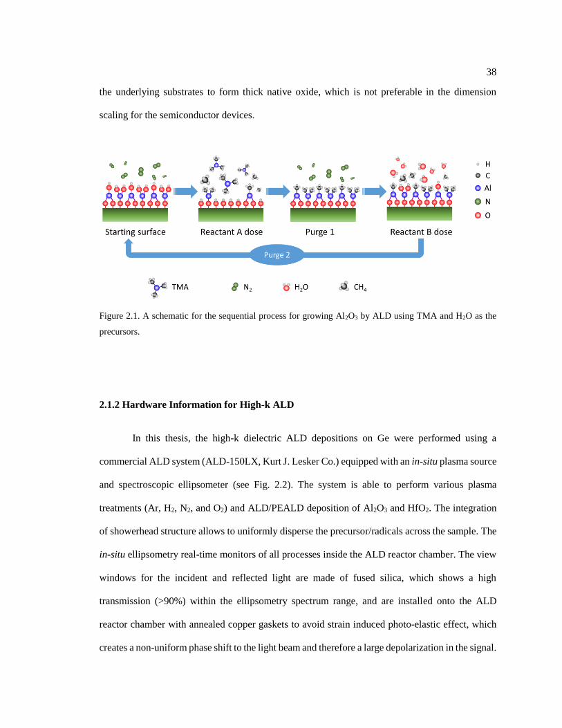
38
the underlying substrates to form thick native oxide, which is not preferable in the dimension
scaling for the semiconductor devices.
Figure 2.1. A schematic for the sequential process for growing Al2O3 by ALD using TMA and H2O as the
precursors.
2.1.2 Hardware Information for High-k ALD
In this thesis, the high-k dielectric ALD depositions on Ge were performed using a
commercial ALD system (ALD-150LX, Kurt J. Lesker Co.) equipped with an in-situ plasma source
and spectroscopic ellipsometer (see Fig. 2.2). The system is able to perform various plasma
treatments (Ar, H2, N2, and O2) and ALD/PEALD deposition of Al2O3 and HfO2. The integration
of showerhead structure allows to uniformly disperse the precursor/radicals across the sample. The
in-situ ellipsometry real-time monitors of all processes inside the ALD reactor chamber. The view
windows for the incident and reflected light are made of fused silica, which shows a high
transmission (>90%) within the ellipsometry spectrum range, and are installed onto the ALD
reactor chamber with annealed copper gaskets to avoid strain induced photo-elastic effect, which
creates a non-uniform phase shift to the light beam and therefore a large depolarization in the signal.

39
The process parameters used in this thesis are as follows. The substrate temperature ranges
from 110-330 °C. The process background pressure is typically ~1.2 Torr Ar gas. A carrier gas of
Ar is used to deliver all precursors and the plasma radicals. The detailed parameters for the thermal
ALD of Al2O3 and HfO2 and the plasma treatments are shown in Tab. 2.1 and 2.2, respectively.
Table 2.1. Parameters for the precursors used in thermal ALD.
Precursor Source
Temp. (°C)
Carrier Gas
Flow (sccm)
Dose
Time (sec)
Purge
Time (sec)
TMA 20 20 0.04 10
TDMAH 85 20 0.2 10
H2O 20 20 0.3 20
Table 2.2. Parameters for the plasma treatments.
Plasma Type Reactive Gas
Flow (sccm)
Carrier Gas
Flow (sccm)
Power
(Watt)
Dose
Time (sec)
O2 (pulse) 3 117 125 1.75
O2 (continuum) 3 117 125 ≥5
H2 (low power) 3 117 125 ≥5
H2 (high power) 8 112 300 ≥5
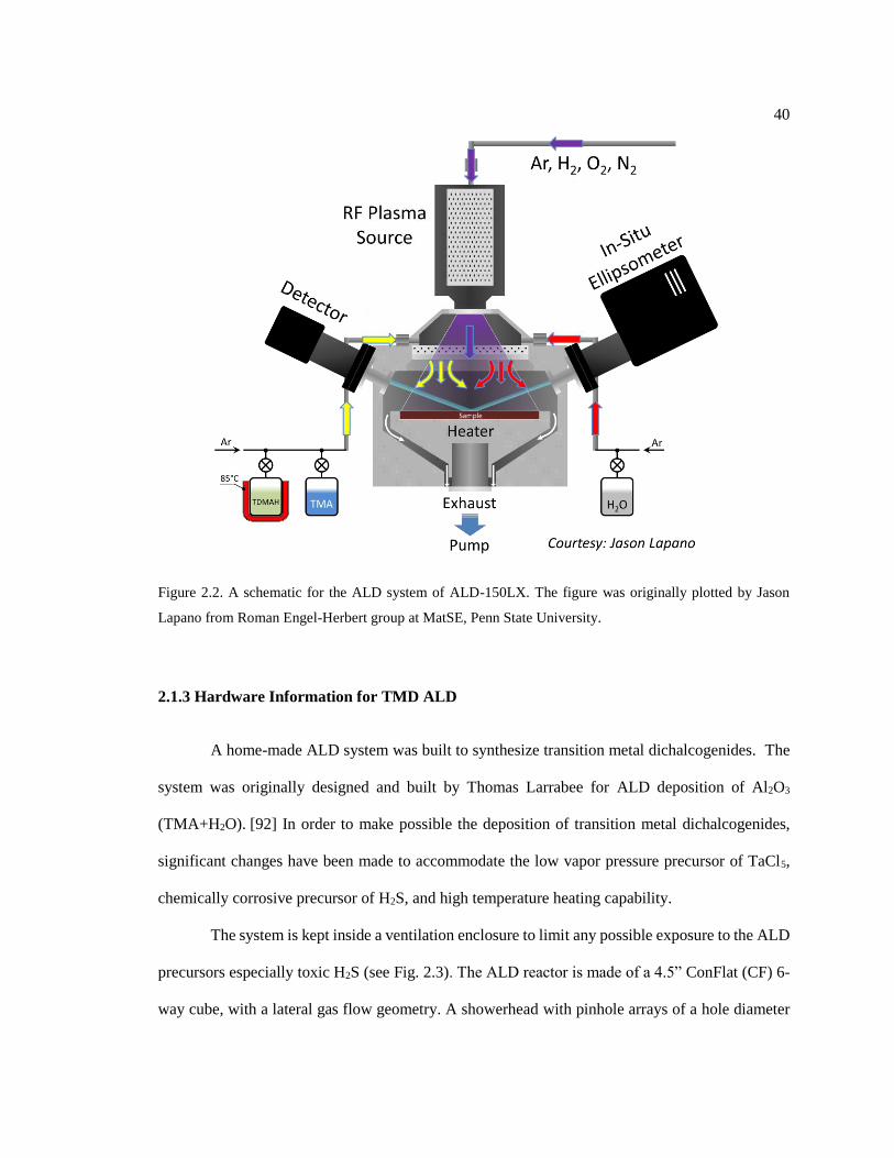
40
Figure 2.2. A schematic for the ALD system of ALD-150LX. The figure was originally plotted by Jason
Lapano from Roman Engel-Herbert group at MatSE, Penn State University.
2.1.3 Hardware Information for TMD ALD
A home-made ALD system was built to synthesize transition metal dichalcogenides. The
system was originally designed and built by Thomas Larrabee for ALD deposition of Al2O3
(TMA+H2O). [92] In order to make possible the deposition of transition metal dichalcogenides,
significant changes have been made to accommodate the low vapor pressure precursor of TaCl5,
chemically corrosive precursor of H2S, and high temperature heating capability.
The system is kept inside a ventilation enclosure to limit any possible exposure to the ALD
precursors especially toxic H2S (see Fig. 2.3). The ALD reactor is made of a 4.5” ConFlat (CF) 6-
way cube, with a lateral gas flow geometry. A showerhead with pinhole arrays of a hole diameter

41
Ø=0.06” and spacing d=0.15” was machined out of an Al metal disk (diameter Ø=2.5” and
thickness t=0.5”), mounted into a double-faced CF 4.5” flange (see Fig. 2.4), and used to uniformly
disperse the gas flow inside the ALD reactor. The heater of the ALD system was also home-made
(see Fig. 2.5). In order to minimize the heat sink effect due to the air exposure of the backside of
the bottom flange, the heater stage (0.9”×0.9”) is not in direct contact with the bottom flange but
suspended by long studs. A heater cartridge (Zoro, Ø=0.5”, 191 Watts/inch2) is used to heat the
stage. A K-type thermocouple is mounted near the heater cartridge to measure the temperature of
the sample stage. An in-situ self-heated quartz crystal microbalance (QCM) is installed to monitor
the ALD growth. An oscillator is used to find the resonant frequency which is then measured by
the frequency counter. Details about the QCM setup can be found in Ref. [92]. Note that the
pressure gauge is installed at the downstream of gas flow in order to avoid the degassing
contamination from the gauge to the ALD reactor chamber. The carrier gas flows are both 40 sccm
Ar for both dosing lines, and yield a background pressure of ~1.03 Torr.
H2S source is kept at in a lecture bottle and its flow is limited using a high-pressure mass
flow controller (MFC, 100 sccm max), due to the high vapor pressure of H2S (~252 PSI at 20 °C).
To avoid the corrosion from H2S exposure to the vacuum sealing, silver-plated gaskets are used for
CF flange sealing, and stainless steel VCR gaskets are used for VCR connections. Also, to protect
the inner wall of the ALD reactor from H2S, a thick Al2O3 coating layer (~ 1 m) has been deposited
by ALD (TMA+H2O) in the reactor chamber. Pneumatic ALD valves are used to control the dose
time of precursors with a time resolution of 10 ms. In the real ALD growth, a H2S flow rate of 1
sccm and a dose time of 15 ms are used to generate a dose pressure of ~500 mTorr.
A by-pass loop structure is used for TaCl5, so as to introduce a through flow to purge the
ALD valves to avoid clogging that may be caused by cold condensation. The TaCl5 source cylinder
is kept at 120 °C to generate a sufficient vapor pressure. The vapor pressure of TaCl5 is given
by: [93]
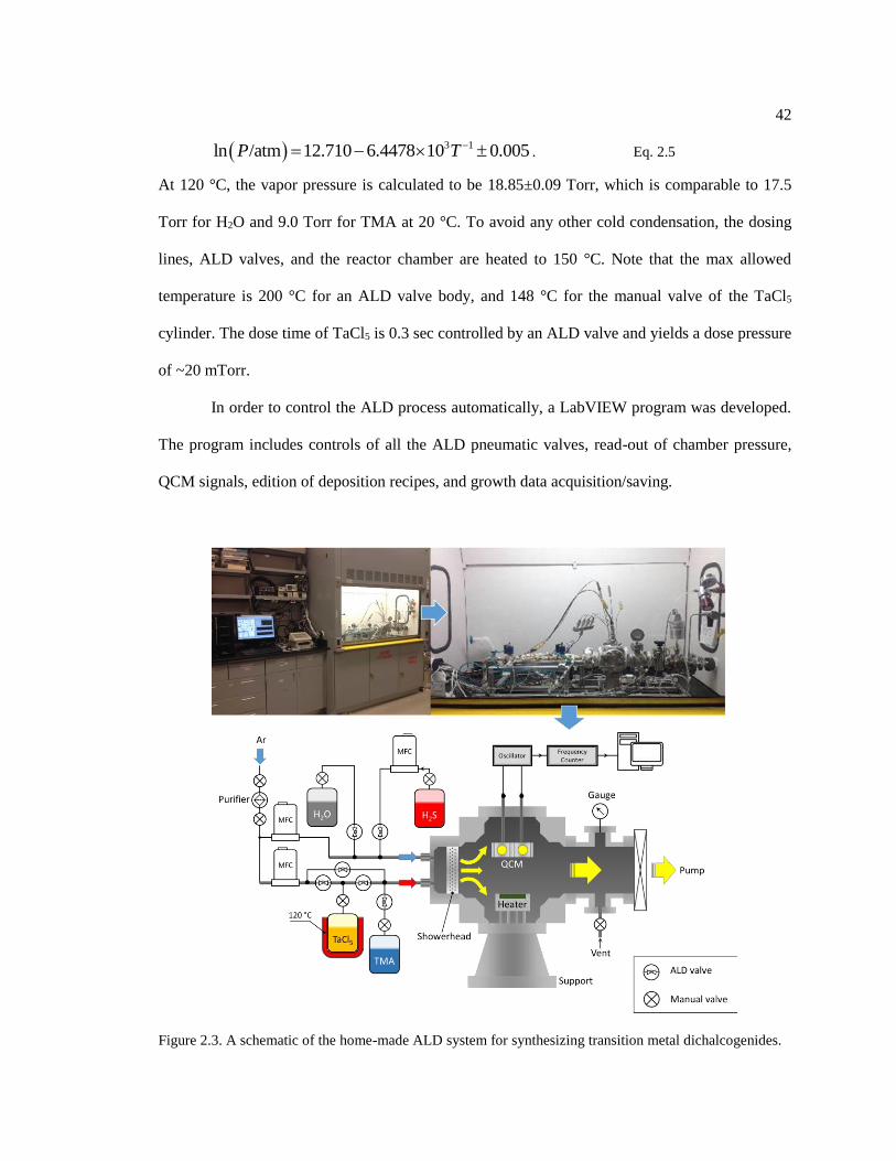
42
3 1ln /atm 12.710 6.4478 10 0.005P T . Eq. 2.5
At 120 °C, the vapor pressure is calculated to be 18.85±0.09 Torr, which is comparable to 17.5
Torr for H2O and 9.0 Torr for TMA at 20 °C. To avoid any other cold condensation, the dosing
lines, ALD valves, and the reactor chamber are heated to 150 °C. Note that the max allowed
temperature is 200 °C for an ALD valve body, and 148 °C for the manual valve of the TaCl5
cylinder. The dose time of TaCl5 is 0.3 sec controlled by an ALD valve and yields a dose pressure
of ~20 mTorr.
In order to control the ALD process automatically, a LabVIEW program was developed.
The program includes controls of all the ALD pneumatic valves, read-out of chamber pressure,
QCM signals, edition of deposition recipes, and growth data acquisition/saving.
Figure 2.3. A schematic of the home-made ALD system for synthesizing transition metal dichalcogenides.
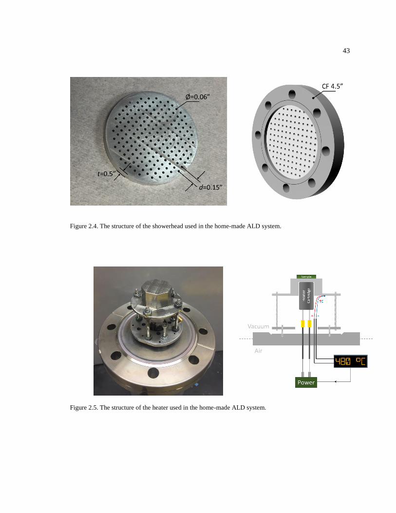
43
Figure 2.4. The structure of the showerhead used in the home-made ALD system.
Figure 2.5. The structure of the heater used in the home-made ALD system.

44
2.2 Spectroscopic Ellipsometry
Spectroscopic Ellipsometry (SE) is an optical measurement of the near-surface dielectric
properties of materials. SE has been widely used in both manufacturing [94] and academic
researches. [95] SE measurement is a non-invasive, low cost, and fast characterization technique.
These advantageous features allows its application for both ex-situ and in-situ measurement in
surface-related processes. In particular, in-situ SE has been a powerful tool for real time monitoring
the deposition and etching, because of its high sensitivity to surface changes, especially film
thickness (sub-Angstrom resolution).
Early application of ellipsometry was not spectroscopic, namely monochromatic or using
only a few wavelengths in the light source to determine the optical constants of the materials. This
can result in multiple solutions when numerically de-convoluting for the material optical constants
and thin film thickness, especially for a non-standard material with unknown optical constants or
modified materials somewhat deviating from the standard properties. For example, the refractive
index n of Al2O3 grown by ALD is temperature dependent (e.g. n=1.77 at 600 nm for 270 °C, and
n=1.52 for 110 °C), while the growth rate is also sensitive to the temperature, so it become difficult
to solve for both refractive indexes and growth rates at the same time. In real applications, SE is
more advanced wherein a broad range light source is utilized to obtain a continuous spectrum, and
an optical model with well-defined dispersion relations (corresponding to the optical transitions in
the materials) is adopted to fit the spectrum. Thus, the material parameters given by SE are de-
convoluted with more constraints and more physically meaningful.
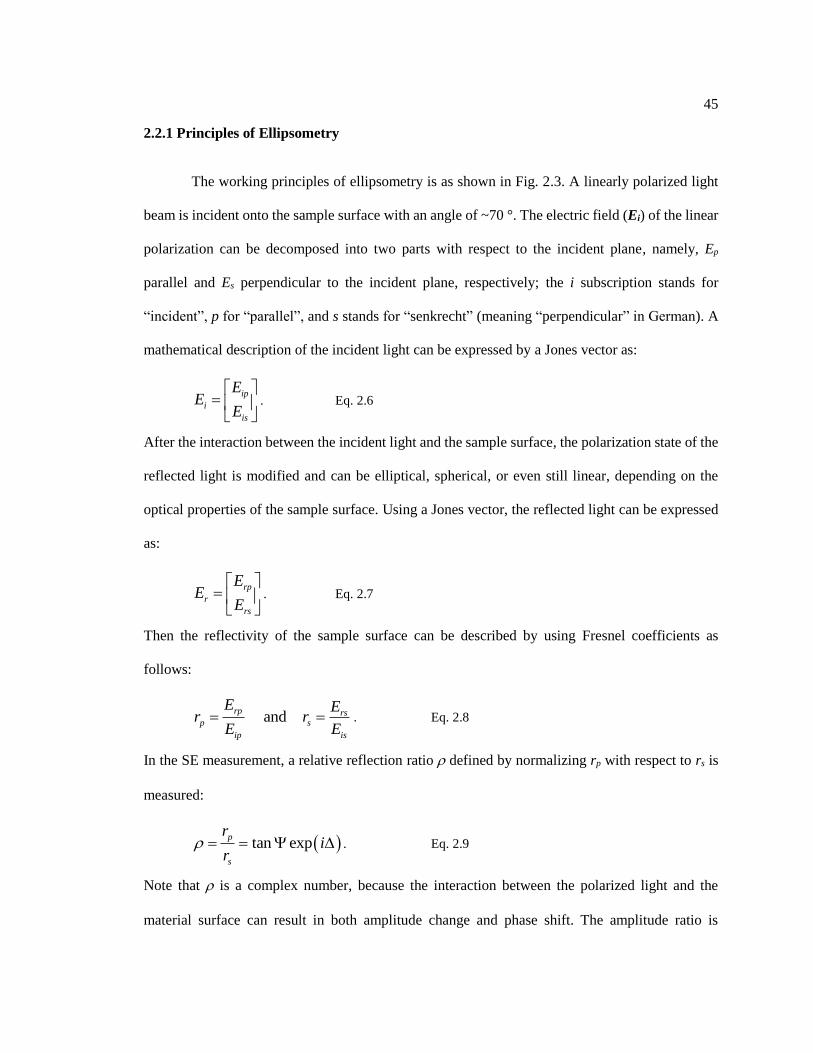
45
2.2.1 Principles of Ellipsometry
The working principles of ellipsometry is as shown in Fig. 2.3. A linearly polarized light
beam is incident onto the sample surface with an angle of ~70 °. The electric field (Ei) of the linear
polarization can be decomposed into two parts with respect to the incident plane, namely, Ep
parallel and Es perpendicular to the incident plane, respectively; the i subscription stands for
“incident”, p for “parallel”, and s stands for “senkrecht” (meaning “perpendicular” in German). A
mathematical description of the incident light can be expressed by a Jones vector as:
ip
i
is
EE
E
. Eq. 2.6
After the interaction between the incident light and the sample surface, the polarization state of the
reflected light is modified and can be elliptical, spherical, or even still linear, depending on the
optical properties of the sample surface. Using a Jones vector, the reflected light can be expressed
as:
rp
r
rs
EE
E
. Eq. 2.7
Then the reflectivity of the sample surface can be described by using Fresnel coefficients as
follows:
and rp rs
p s
ip is
E Er r
E E . Eq. 2.8
In the SE measurement, a relative reflection ratio defined by normalizing rp with respect to rs is
measured:
tan expp
s
ri
r . Eq. 2.9
Note that is a complex number, because the interaction between the polarized light and the
material surface can result in both amplitude change and phase shift. The amplitude ratio is

46
represented by tan, while the phase by exp(i). and are the two primary parameters of SE
measurement, and defined as ellipsometric angles. Since these two angles essentially describes the
interaction between the light and sample, we can use a Jones matrix to represent the sample:
tan exp 0 sin exp 0 or
0 1 0 cos
i iS
. Eq. 2.10
Fig. 2.4 shows the optics for measuring a simple homostructure sample with a flat surface
and sufficient thickness (so that no backside reflection). Usually, the medium (0) in the SE
measurements is either air or vacuum, so we can simply the measurement by approximating the
refractive index for medium (0) as n0=1, k0=0. Then from Fresnel equations, the relation between
the ellipsometric angles / and the refractive index n/k of the homostructure sample can be
expressed as follows: [96]
2 2
0 0
tan 1 4sin tan exp 2 tan exp tan exp
1 tan exp
i i i i in ik n ik
i
2 2tan 1 4sin tan exp 2 tan exp tan exp
1 tan exp
i i i i i
i
. Eq. 2.11
So we can directly determine the optical constants of the materials in homostructure samples. This
strategy works well for measuring absorbing substrate samples like Si and Ge, where the surface is
clean, atomically flat and thickness (≥200 m) is sufficient to avoid the transmission to the sample
backside and cause coherent backside reflection that will result in the depolarization of the
measurement signal (see Fig. 2.5a). For non-absorbing substrates like sapphire and SrTiO3, it is
necessary to roughen the backside to randomly scatter the transmitted light so as to eliminate the
backside reflection, e.g. using single-side polished substrates. Particularly, note in that in an
infrared (IR) light range, even substrates like Si are transparent, so the backside reflection effect is
still non-trivial (see Fig. 2.5b).
Fig. 2.6 shows the optics for measuring a heterostructure sample with a thin film overlayer
on a thick substrate. In this measurement, two interfaces are present, one between the film and
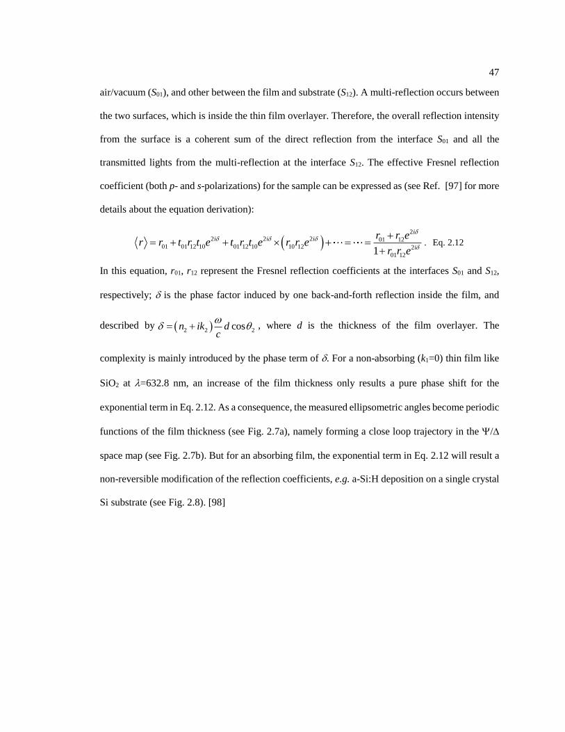
47
air/vacuum (S01), and other between the film and substrate (S12). A multi-reflection occurs between
the two surfaces, which is inside the thin film overlayer. Therefore, the overall reflection intensity
from the surface is a coherent sum of the direct reflection from the interface S01 and all the
transmitted lights from the multi-reflection at the interface S12. The effective Fresnel reflection
coefficient (both p- and s-polarizations) for the sample can be expressed as (see Ref. [97] for more
details about the equation derivation):
2
2 2 2 01 1201 01 12 10 01 12 10 10 12 2
01 121
ii i i
i
r r er r t r t e t r t e r r e
r r e
. Eq. 2.12
In this equation, r01, r12 represent the Fresnel reflection coefficients at the interfaces S01 and S12,
respectively; is the phase factor induced by one back-and-forth reflection inside the film, and
described by 2 2 2cosn ik dc
, where d is the thickness of the film overlayer. The
complexity is mainly introduced by the phase term of . For a non-absorbing (k1=0) thin film like
SiO2 at =632.8 nm, an increase of the film thickness only results a pure phase shift for the
exponential term in Eq. 2.12. As a consequence, the measured ellipsometric angles become periodic
functions of the film thickness (see Fig. 2.7a), namely forming a close loop trajectory in the /
space map (see Fig. 2.7b). But for an absorbing film, the exponential term in Eq. 2.12 will result a
non-reversible modification of the reflection coefficients, e.g. a-Si:H deposition on a single crystal
Si substrate (see Fig. 2.8). [98]
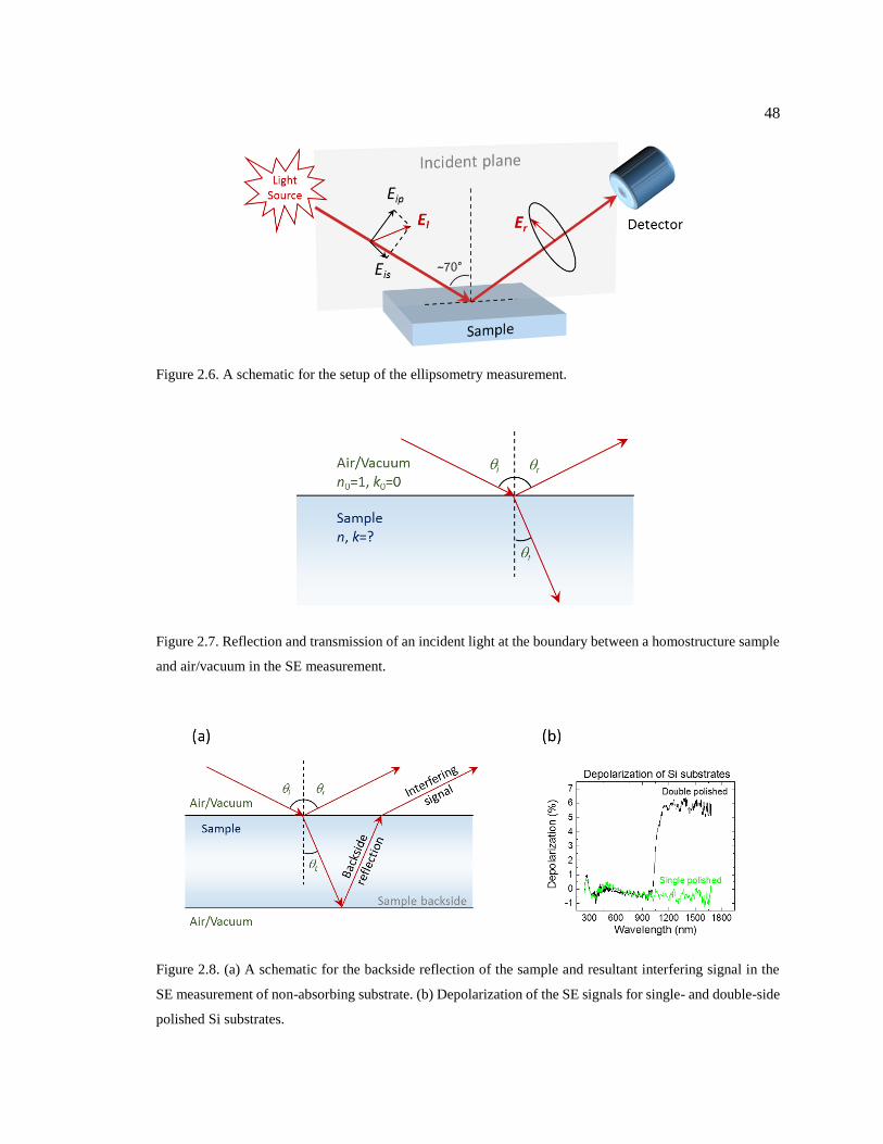
48
Figure 2.6. A schematic for the setup of the ellipsometry measurement.
Figure 2.7. Reflection and transmission of an incident light at the boundary between a homostructure sample
and air/vacuum in the SE measurement.
Figure 2.8. (a) A schematic for the backside reflection of the sample and resultant interfering signal in the
SE measurement of non-absorbing substrate. (b) Depolarization of the SE signals for single- and double-side
polished Si substrates.
49
2.2.2 Data Analysis
While analyzing the SE results for a homostructure sample can be done simply using Eq.
2.11, a direct analysis for multilayer-film samples is not straightforward because too many fitting
parameters in the structural model may results in completely random convergence into local
minimum with false outcomes. To obtain a reliable global minimum, a practical strategy is “bottom
up”, namely measure and fit layer-by-layer (see Fig. 2.9). Firstly, prepare a pristine substrate with
atomic flatness and contaminant-free. During the measurement, we need to assure that the surface
will be not contaminated again, so in-situ cleans and in-situ measurements are preferred. The
optical constants of the substrate (n0/k0) can be extracted using Eq. 2.11. Then, deposit the first film
overlayer (1), perform the SE measurement. With the optically defined substrate, we can now fit
for the optical constants (n1/k1) and thickness (d1) for the film (1). Following the same steps, we
can layer-by-layer extract the information of the film (2), (3) and so forth. The advantage of this
bottom-up strategy is that in each fitting process, there is only one unknown layer, so with fewer
parameters, the randomness of fitting can be significantly suppressed.
Various optical models are used to describe the energy dispersion of the dielectric function
(see Fig. 2.10). In general, a physical requirement for these models is the satisfactory of Kramers-
Kronig relation between the e1 and e2 in the modeling. [97] A classical description of the optical
transition is Lorentz model, wherein the electron interacts with the electric field of the light like an
oscillator around the nucleus. [97] The contribution of a single Lorentz oscillator to the dielectric
function is as follows (also see Fig. 2.11a):
01 2 2 2
0
Ei A
E E i E
. Eq. 2.13
In this equation, E is the photon energy, E0 is the resonant energy or the transition peak position,
is the peak broadening caused by damping, and A is the dimensionless amplitude. For multi Lorentz
50
oscillators, the overall dielectric function of the material can be expressed as a simple sum of all
oscillators (j=1, 2, 3 …) and the vacuum (1=1, 2=0), as follows:
1 21 j j
j
i . Eq. 2.14
For transparent materials (k, 2~0), namely the spectrum range is way lower in energy than
the transition peak positions (<<E0-E), the measured SE spectrum is the low energy tail of the
optical transitions, and can be described by a series expansion of Lorentz model as a function of
wavelength. This simplified model is called Sellmeier for describing 1 or Cauchy for n. In this
thesis, the Cauchy model is used for describing all the oxides grown by ALD, as follows:
2 4
and 0B C
n A k
. Eq. 2.15
is the wavelength number in nm. The Cauchy model is purely a mathematical approximation of
the real refractive index. Usually, a good evaluation can be achieved using up to the second order
approximation, namely only A, B, and C. Fig. 2.11b shows the Cauchy dispersion for Al2O3.
For asymmetric optical transitions caused by the cut-off effect of the band gap (Eg) of
materials, a modified Lorentz model, Tauc-Lorentz (TL), [99] is used as follows (also see Fig.
2.11c):
2
0
22 2 2 2
2
for
0 for
g
g
g
g
E E EAE E
EE E E E
E E
. Eq. 2.16
Note that the amplitude A is of an energy dimension, namely in eV. The contribution of the TL
oscillator to real part of dielectric function (1) is obtained by the Kramers-Kronig integration of
2, as follows:
2
1 2 2
2
gEE P d
E
. Eq. 2.17
P stands for the principal of the integral. The use of TL oscillators is necessary for describing the
major peaks in the dielectric functions, because the position of the band gap produces major
51
modification to the peak profile. But for minor peaks, a TL model does not significantly improve
the fitting quality compared to using a simple Lorentz model in the ultimate fitting results, because
of their low spectral weight, but just increase the complexity of fitting by increasing the number of
variables.
Other commonly used models include Drude model for describing the intraband transitions
in metallic/conducting materials at low energies, and effective medium approximation (EMA) to
describe the interface/surface roughness layer by mixing the dielectric functions of two or more
materials to form an intermediate material. These two models are not used in this thesis, so not
discussed in details. More information about them can be found in Ref. [96,97]. Also, all the
materials characterized by ellipsometry in this thesis are isotropic, so were measured by a standard
mode of ellipsometry. More details about measuring anisotropic materials can be found in
Ref. [96,97].
General steps for fitting absorbing film materials with generalized oscillators (namely
using Lorentz, TL, Drude, etc) are as follows: (1) Prepare a target film sample with a sufficient
thickness (≥ 5nm; the thicker, the better). (2) Precisely measure the film thickness with other
characterization methods, like X-ray diffraction (XRD), tunneling electron microscopy (TEM), or
atomic force microscopy (AFM), with an Angstrom-level thickness resolution. (3) Start fitting with
a B-spline model (choose a similar material as the starting n/k, and an energy step of ≤0.1 eV) to
obtain a raw dielectric function of the material; B-spline model is essentially a point-by-point
calculation of dielectric function or refractive indexes using Fresnel equations; in this calculation,
various combination of n/k and thickness can result in the same /, so a precise measurement of
the thickness becomes important in uniquely determining n/k or the dielectric function. (4)
Parameterize the imaginary part of raw dielectric function e2 with the generalized oscillators. (5)
Parameterize the real part of raw dielectric function e1; if the fitting of e2 is done properly, the mis-
fitting for e1 is usually an overall offset which can be simply corrected by fitting the high energy
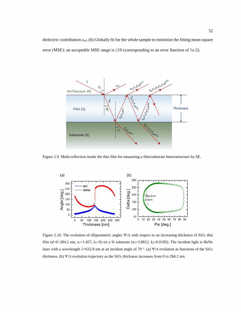
52
dielectric contribution inf. (6) Globally fit for the whole sample to minimize the fitting mean square
error (MSE); an acceptable MSE range is ≤10 (corresponding to an error function of 1e-2).
Figure 2.9. Multi-reflection inside the thin film for measuring a film/substrate heterostructure by SE.
Figure 2.10. The evolution of ellipsometric angles / with respect to an increasing thickness of SiO2 thin
film (d=0~284.2 nm, n1=1.457, k1=0) on a Si substrate (n2=3.8812, k2=0.0195). The incident light is HeNe
laser with a wavelength =632.8 nm at an incident angle of 70 °. (a) /evolution as functions of the SiO2
thickness. (b) /evolution trajectory as the SiO2 thickness increases from 0 to 284.2 nm.

53
Figure 2.11. / evolution trajectory for growing of a-Si:H on a single crystal Si substrate. The refractive
index of a-Si:H is n=5-i0.85 at 500 nm. This figure is reproduces from Ref. [97].
Figure 2.12. Schematic for the bottom-up strategy of characterizing multi-layer structure by SE.
Figure 2.13. Dielectric function models used in ellipsometry data analysis. Figure is copied from Ref. [97].
HOA stands for harmonic oscillator approximation, and MDF for model dielectric function.

54
Figure 2.14. Examples for the dispersion of (a) Lorentz, (b) Cauchy, and (c) Tauc-Lorentz models used in
the ellipsometry data analysis.
2.2.3 Material Parameterization
As will be discussed later, T=270 °C is used as the primary process temperature of high-k
ALD on Ge surface, so the ellipsometry characterization is performed mainly for materials at this
temperature. Tab. 2.3 shows the numerical deconvolution of a clean Ge substrate at T=270 °C using
generalized oscillators (GenOsc). The fitted results are shown in Fig. 2.16, as well as the extracted
dielectric function of Ge. All the amorphous oxide films (GeOx/GeO2, Al2O3, and HfO2) grown in
our processes have high band gaps beyond the spectral range (1.24~5.17 eV), so a Cauchy
dispersion was used to describe their optical constants, as shown in Table 2.4. Note that all the
fitting models used for the oxide films are extracted from relatively thick films (>5 nm) so as to
minimize the error of fitting.
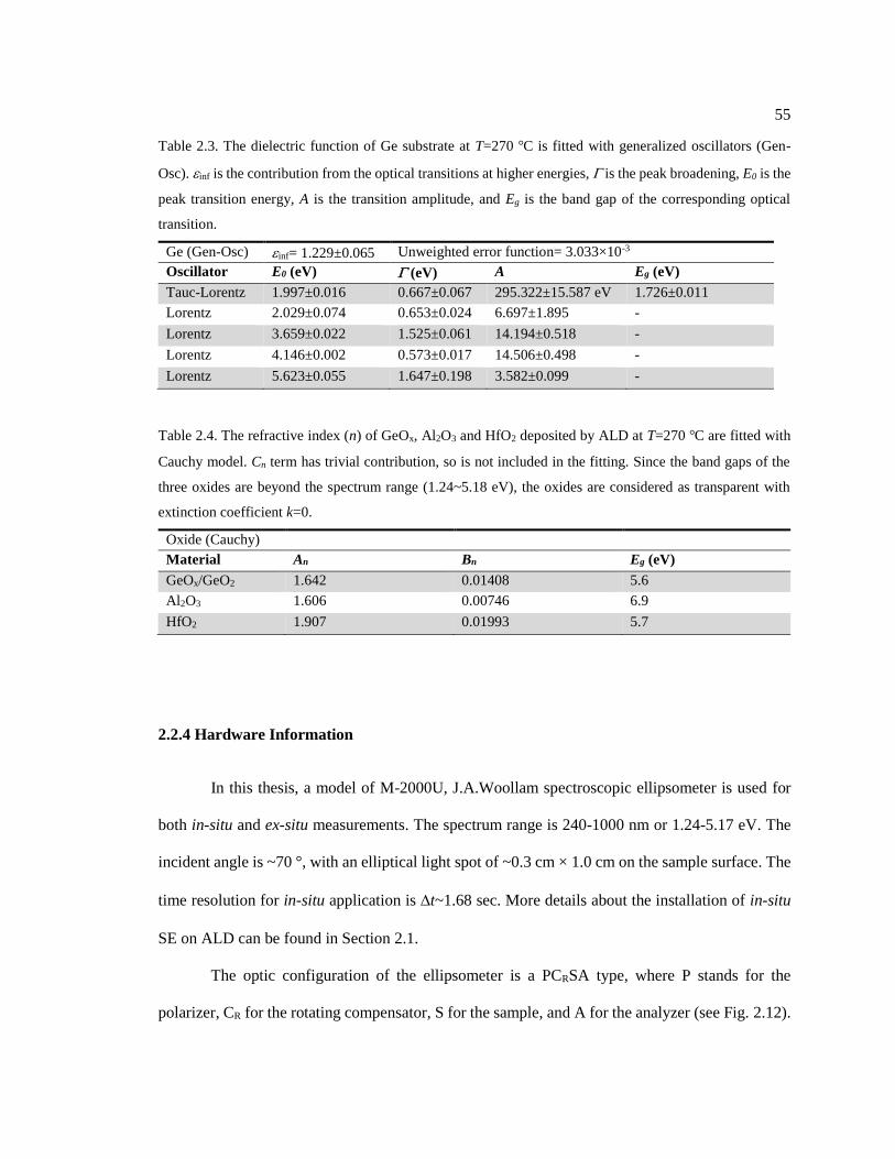
55
Table 2.3. The dielectric function of Ge substrate at T=270 °C is fitted with generalized oscillators (Gen-
Osc). inf is the contribution from the optical transitions at higher energies, is the peak broadening, E0 is the
peak transition energy, A is the transition amplitude, and Eg is the band gap of the corresponding optical
transition.
Ge (Gen-Osc) inf= 1.229±0.065 Unweighted error function= 3.033×10⁻³
Oscillator E0 (eV) (eV) A Eg (eV)
Tauc-Lorentz 1.997±0.016 0.667±0.067 295.322±15.587 eV 1.726±0.011
Lorentz 2.029±0.074 0.653±0.024 6.697±1.895 -
Lorentz 3.659±0.022 1.525±0.061 14.194±0.518 -
Lorentz 4.146±0.002 0.573±0.017 14.506±0.498 -
Lorentz 5.623±0.055 1.647±0.198 3.582±0.099 -
Table 2.4. The refractive index (n) of GeOx, Al2O3 and HfO2 deposited by ALD at T=270 °C are fitted with
Cauchy model. Cn term has trivial contribution, so is not included in the fitting. Since the band gaps of the
three oxides are beyond the spectrum range (1.24~5.18 eV), the oxides are considered as transparent with
extinction coefficient k=0.
Oxide (Cauchy)
Material An Bn Eg (eV)
GeOx/GeO2 1.642 0.01408 5.6
Al2O3 1.606 0.00746 6.9
HfO2 1.907 0.01993 5.7
2.2.4 Hardware Information
In this thesis, a model of M-2000U, J.A.Woollam spectroscopic ellipsometer is used for
both in-situ and ex-situ measurements. The spectrum range is 240-1000 nm or 1.24-5.17 eV. The
incident angle is ~70 °, with an elliptical light spot of ~0.3 cm × 1.0 cm on the sample surface. The
time resolution for in-situ application is t~1.68 sec. More details about the installation of in-situ
SE on ALD can be found in Section 2.1.
The optic configuration of the ellipsometer is a PCRSA type, where P stands for the
polarizer, CR for the rotating compensator, S for the sample, and A for the analyzer (see Fig. 2.12).
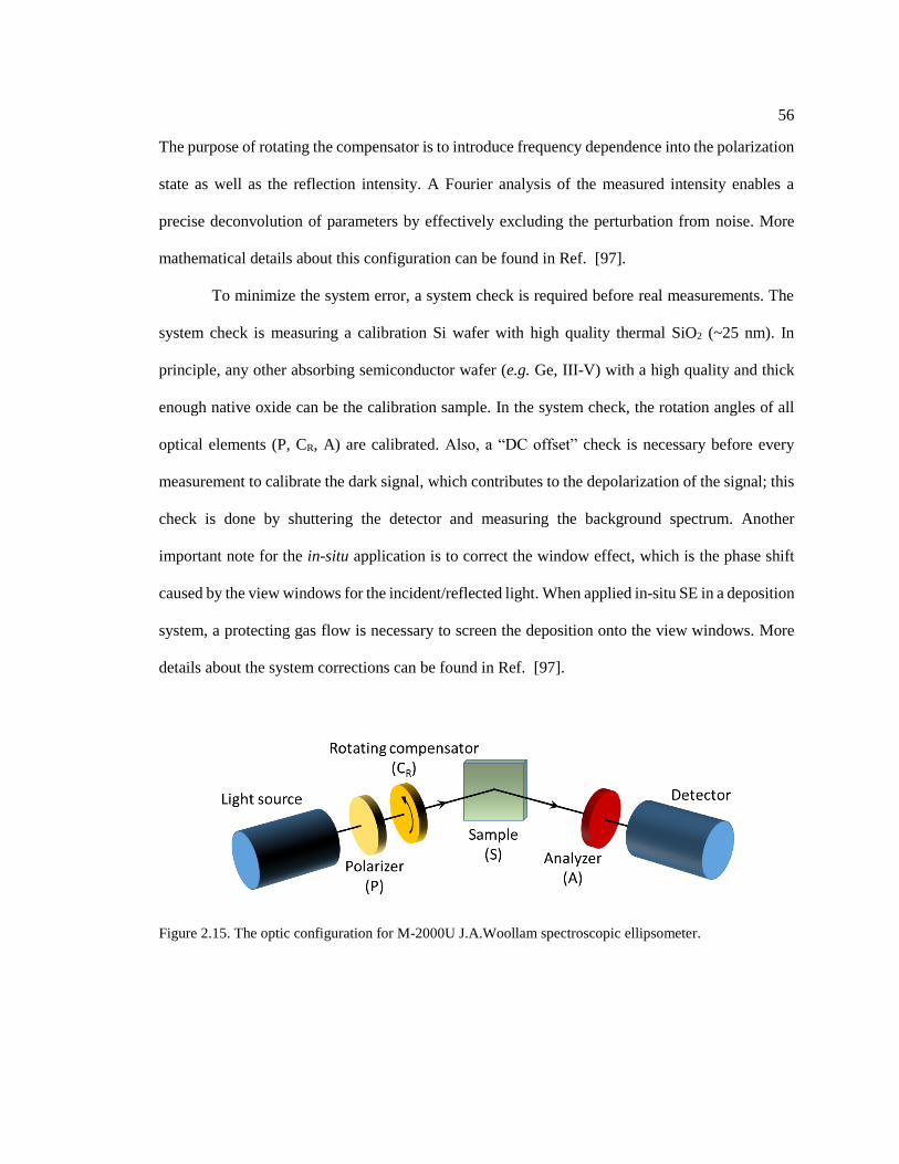
56
The purpose of rotating the compensator is to introduce frequency dependence into the polarization
state as well as the reflection intensity. A Fourier analysis of the measured intensity enables a
precise deconvolution of parameters by effectively excluding the perturbation from noise. More
mathematical details about this configuration can be found in Ref. [97].
To minimize the system error, a system check is required before real measurements. The
system check is measuring a calibration Si wafer with high quality thermal SiO2 (~25 nm). In
principle, any other absorbing semiconductor wafer (e.g. Ge, III-V) with a high quality and thick
enough native oxide can be the calibration sample. In the system check, the rotation angles of all
optical elements (P, CR, A) are calibrated. Also, a “DC offset” check is necessary before every
measurement to calibrate the dark signal, which contributes to the depolarization of the signal; this
check is done by shuttering the detector and measuring the background spectrum. Another
important note for the in-situ application is to correct the window effect, which is the phase shift
caused by the view windows for the incident/reflected light. When applied in-situ SE in a deposition
system, a protecting gas flow is necessary to screen the deposition onto the view windows. More
details about the system corrections can be found in Ref. [97].
Figure 2.15. The optic configuration for M-2000U J.A.Woollam spectroscopic ellipsometer.
57
2.3 Admittance Characterization
2.3.1 Principles of MOSCap Admittance
In this thesis, metal-oxide-semiconductor capacitor (MOSCap) devices were fabricated to
electrically characterize the dielectric/Ge interface properties. The structure of a MOSCap is shown
in Fig. 2.16a, which is a multilayer stacking on a semiconductor substrate. In this structure, the top
metal layer is used as the gate electrode on which a gate voltage (VG) is applied to tune the electrical
properties of the device. The oxide layer is the gate dielectric to isolate the gate metal from the
semiconductor channel but still allow the electric field to penetrate through; the gate dielectric can
also be other insulators like nitrides and oxynitrides. Compared to the above-mentioned MOSFET
structure, MOSCap is simpler without the source and drain (S/D) terminals. The equivalent circuit
of a MOSCap can be represented by conductor (G) and capacitor (C) in parallel (see Fig. 2.17a).
The admittance (Y) (or impedance Z=1/Y) of MOSCap are measured using a combination of DC
bias voltage and a small AC voltage (typically VRMS=10-50 mV). The admittance of the MOSCap
can be expressed as follows:
Y G j C . Eq. 2.18
is the angular frequency of AC voltage. The capacitance C is the dielectric response to the AC
voltage at certain DC bias, so C=dQ/dV. The overall capacitance of a MOSCap device is comprised
of two parts in series, oxide capacitance (Cox) and semiconductor capacitance (Cs), as shown in Fig.
2.17b. The oxide capacitance Cox is constant and expressed as:
oxox
ox
Ct
. Eq. 2.19
ox is the dielectric constant of the gate oxide, while tox is the thickness. In quantifying the oxide
capacitance Cox made of high-k dielectrics like HfO2, a more convenient description is to normalize

58
the oxide thickness with respect to SiO2, and obtain an equivalent oxide thickness (EOT) as
follows: [100]
2
2
0 20 3.4515F/cm
EOT/nm
SiOox oxox
SiOox ox
ox
ox
kkC
kt tt
k
. Eq. 2.20
kox and kSiO2 are the relative dielectric constant of the gate oxide and SiO2, and kSiO2=3.9. The
semiconductor capacitance Cs originates from the fact that electric field can exist and therefore
electric charge can be spatially stored in semiconductors. The semiconductor capacitance Cs varies
with the gate voltage due to the electric gating effect on the semiconductor, as will be discussed in
details later. The measured overall capacitance of the device (Cstack) can be expressed as follows:
1 1 1
stack ox sC C C . Eq. 2.21
Fig. 2.18 shows the simulations for an ideal p-type MOSCap device at various gate
voltages. In Fig. 2.18a, with a sufficient negative DC gate voltage VG and grounding the
semiconductor bulk, the potential difference between the two sides of the gate oxide induces an
electric field in the oxide. The electric field penetrates into the near interface semiconductor, and
consequently induces band up-bending. The relative position of the Fermi level EF with respect to
the bended band results in an accumulation of hole, namely a high density of holes is stored in the
near-interface semiconductor, so the semiconductor capacitance Cs becomes significantly larger
than the oxide capacitance Cox, that is, Cs >> Cox. From Eq. 2.21, the measured overall capacitance
becomes Cstack Cox= Cmax. So by checking the maximum capacitance Cmax from the measured
capacitance vs voltage (C-V) curve, the oxide capacitance Cox can be obtained, from which EOT of
the gate oxide can be derived using Eq. 2.20.
In Fig. 2.18b, a less negative voltage VG is applied on the gate metal, and is matching the
difference between the work function of the gate metal and the Fermi level EF of the semiconductor.
As a result, there is no bend banding or induced charge in either the gate metal or the semiconductor.
59
This stage is called a flat-band (FB) condition. There is a smaller semiconductor capacitance Cs
given by:
2
, where Debye length s Sis D
D a
kTC L
L q N
. Eq. 2.22
So if the doping concentration Na is known, the stack capacitance at the flat-band condition (CFB)
can be obtained by combining Eq. 2.21 and 2.22. Then by checking the measured C-V curve, the
flat-band voltage (VFB) can be obtained. Note for the Ge substrates used in this thesis (Na=0.66-
3.3e15 cm-3), the Debye length at room temperature is estimated to be LD=83.5-186.7 nm.
As the gate voltage becomes even less negative beyond the flat-band condition, down-
bending of the semiconductor occurs (see Fig. 2.18c). As a consequence, the doping carrier or
majority carrier is depleted and a space charge region is created near the interface, which is called
“depletion region” with a width of xd. The maximum depletion width is determined by the doping
concentration Na as follows:
2
4ln /s
dm a i
a
kTx N n
q N
. Eq. 2.23
For example, in a moderately doped p-Si with Na= 3.3e17 cm-3, xdm ~59.4 nm. The resultant
semiconductor capacitance Cs is given by:
2 s
s
dm
Cx
. Eq. 2.24
From this equation, the relatively large depletion width xdm results in a small capacitance density
Cs. From Eq. 2.21, the stack capacitance Cstack is minimized, i.e. Cstack= Cmin. So a measurement of
Cmin, the maximum depletion width xdm can be derived by combining Eq. 2.21 and 2.24 with a
known oxide capacitance Cox, and therefore the doping concentration Na can be obtained.
When a sufficient positive gate voltage VG is applied to a p-MOSCap (see Fig. 2.18d),
further down-bending of the semiconductor band results in an inversion from a majority-carrier
(hole) dominant type into minority-carrier (electron) dominance. The threshold condition of this

60
inversion condition is when the induced electron concentration is comparable to the doping
concentration with a semiconductor band bending (s) as follows:
2
ln as
i
NkTthreshold
q n
. Eq. 2.25
This is also when the depletion width xd is maximized (see Eq. 2.23). Beyond the threshold voltage
(Vth), a high density of electrons is induced and stored in the near-interface semiconductor region,
namely the inversion region. As a result, the semiconductor capacitance Cs becomes significantly
large again, i.e. Cs >> Cox, and therefore the stack capacitance Cstack Cox. But this requires a
sufficient delay time for the device to respond to the gate voltage to generate enough minority
carriers (electrons in p-type semiconductors):
0 02 / , where is minority-carrier lifetime.a it N n Eq. 2.26
Typically, the minority response time is 0.1-10 sec. [1] The response time for the Ge substrates
used in this thesis (Na ~ 2e15 cm-3, 0 ~ 0.001 sec) is ~0.2 sec. So in the inversion region, the
minority-carriers (electron in p-type semiconductors) cannot respond to AC signal with frequencies
>100 Hz, while only majority-carriers (depletion charge) contribute to the semiconductor
capacitance, similar to Eq. 2.24. So a high frequency C-V measurement will detect a minimized
stack capacitance, i.e. Cstack = Cmin, as indicated by the dash line in the C-V simulations in Fig.
2.18d.
Figure 2.16. (a) Equivalent circuit for the admittance measurement of a MOSCap device. (b) The
contributions to the capacitance from the gate oxide and semiconductor.
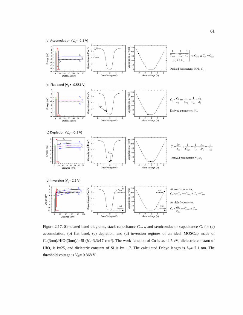
61
Figure 2.17. Simulated band diagrams, stack capacitance Cstack, and semiconductor capacitance Cs for (a)
accumulation, (b) flat band, (c) depletion, and (d) inversion regimes of an ideal MOSCap made of
Cu(3nm)/HfO2(3nm)/p-Si (Na=3.3e17 cm-3). The work function of Cu is m=4.5 eV, dielectric constant of
HfO2 is k=25, and dielectric constant of Si is k=11.7. The calculated Debye length is LD 7.1 nm. The
threshold voltage is Vth= 0.368 V.
62
2.3.2 High Frequency Admittance Measurement
In this thesis, the dielectric/Ge interface properties were characterized by measuring the
device admittance of high frequencies (f= 75 kHz-1.5 MHz). There are two major types of interface
trap states, (i) trap states inside the band gap of the semiconductor which are related to defects from
the near-interface semiconductor region, and (ii) border trap states which locates in the near-
interface dielectric region. Their influence on the admittance of MOSCap devices will be discussed
respectively later.
The density of the trap states inside the band gap is quantified as Dit, which is a density of
state (DOS) for the interface trap states in a unit of cm-2∙eV-1. A major source of the interface traps
is the dangling bonds on the semiconductor surface, with energies usually locating inside the band
gap of the semiconductor. [101] For example, for a clean Si(100) substrate without any overlayer,
each surface Si atom has two dangling bonds, corresponding to a dangling bond density of 2×Si
areal density2.72×1015 cm-2, which corresponds to 2.38×1015 cm-2∙eV-1 after normalizing by the
band gap of Si (EG=1.14 eV at room temperature). This high density of trap states is not acceptable
for the industrial manufacturing of high quality and reliable devices, which require ~×1010 cm-2∙eV-
1 and below. To address this issue, surface passivation is necessary, namely using chemical/physical
approaches to satisfy the dangling bonds so that the trap states are removed or become electrically
inactive. More details about surface passivation will be discussed later.
In admittance measurements, those interface trap states Dit locating inside the band gap of
the semiconductor electrically contribute to the signal. One effect from these interface trap states
(Dit) on MOSCap devices is to stretch out the C-V characteristics (see Fig. 2.19). As mentioned
above, the electrical characteristics of the semiconductor is gated by band bending of the near-
interface semiconductor region and therefore shifting the relative position of the Fermi level EF
inside the band gap. When the Fermi level EF comes across an interface trap state (see Fig. 2.19a),
63
the state becomes electrically active and its charge occupancy is tuned by external voltage, that is,
extra charge needs gating in order to shift the Fermi level EF compared to a clean interface (no Dit).
In other words, there is another capacitor (Cit) formed by the interface trap states involved in the
electric gating. So the gating efficiency on the semiconductor becomes less, and consequently the
response of the stack capacitance Cstack is delayed, namely a stretched C-V curve (see Fig. 2.19b).
The electrical consequence of the stretch-out is the degradation of device speed. The gating time
constant can be estimated as ~ G oxR C , where RG is the gate resistance. The stretch-out results
in an increase of voltage variation VG required to turn on/off the device, therefore increasing the
gating time, i.e. slowing down the device speed.
Another consequence of the interface trap states Dit inside the band gap is the frequency
dispersion in the admittance characteristics. As shown in Fig. 2.20a, when the Fermi level EF
crosses an interface trap state (Eit), the change of charge occupancy is realized by the
communication between the trap state and the majority-carrier band (valence band for a p-type
semiconductor). This exchange process requires a response time (it), given by Shockley-Read-Hall
statistics of capture and emission rates: [102]
exp /
it
t eff
E kT
v N
. Eq. 2.27
In this equation, E=Eit - EV is the energy difference between the trap state and majority-carrier
band edge, is the capture cross section of the trap, vt is the average thermal velocity of the
majority-carriers, Neff is the effective density of states of the majority-carrier band. As a result of
the response time, the interface trap capacitance Cit and conductance Git become frequency
dependent as follows: [103]
64
2
2
2
2
1
1
1
it it
it
it itit
it
C q D
Gq D
. Eq. 2.28
When sweeping in the frequency domain, an admittance measurement (C-V + G-V) allows to map
out the different trap states with various response time it, and therefore figure out the corresponding
energy distribution of the trap states inside the band gap of the semiconductor. From the equivalent
circuit shown in Fig. 2.19a, the frequency dispersion in C-V is more obvious when the MOSCap is
at a depletion status, because the semiconductor capacitance Cs is relatively small. On the other
hand, in accumulation region, the semiconductor capacitance Cs is significantly large and therefore
dominates, so the frequency dispersion caused by the interface trap states diminishes.
Other than compromising the admittance characteristics, the interface trap states reduce the
effective conduction current by trapping the carriers in the MOSFET channel, and also act as
charged scattering centers for the channel carriers near the interface, lowering their effective
mobility. [1]
The second major type of interface trap states are so-called “border traps”. [104,105] These
trap states locate in the band gap of the dielectric and physically distribute in the near-interface
dielectric region. Since the border trap states may be across the whole dielectric thickness, the
density of border trap states (Nbt) is a bulk density in a unit of cm-3∙eV-1. When the Fermi level EF
in the semiconductor crosses a border trap state Nbt, it becomes electrically active and exchange
charge with the accumulation charge (holes in a p-type semiconductor) through a quantum
tunneling mechanism (see Fig. 2.21a). Similar to Eq. 2.27, the response time of the tunneling
process can be written as:
2
0
exp 2e x
bt
t s
x
v N
. Eq. 2.29

65
In this equation, is the capture cross section of the trap, vt is the average thermal velocity of the
accumulation charge, Ns is the carrier density of the surface semiconductor at accumulation, is
the attenuation factor caused by the tunneling effect, as given by: [104]
*2 ox
Vm E E
. Eq. 2.30
ox
VE is the valence band edge of the gate oxide, E is the energy of the accumulation charge carrier,
andox
VE E represents the barrier height of tunneling from the semiconductor to the border trap
state in the dielectric. An equivalent circuit for a MOSCap with border traps is shown in Fig. 2.21b.
Since the border traps spatially locate across the whole gate oxide thickness, the exponential factor
in Eq. 2.29 can cause wide range of the response time, and therefore the admittance of accumulation
region becomes frequency dependent (see Fig. 2.21c). The calculation of the border trap state
density Nbt will be discussed later.
Figure 2.18. (a) The capacitance contributions for a MOSCap device with interface trap states (Dit). Cit
represents the capacitance from the interface trap states Dit. (b) Stretch-out effect in C-V characteristics
caused by the interface trap states Dit.
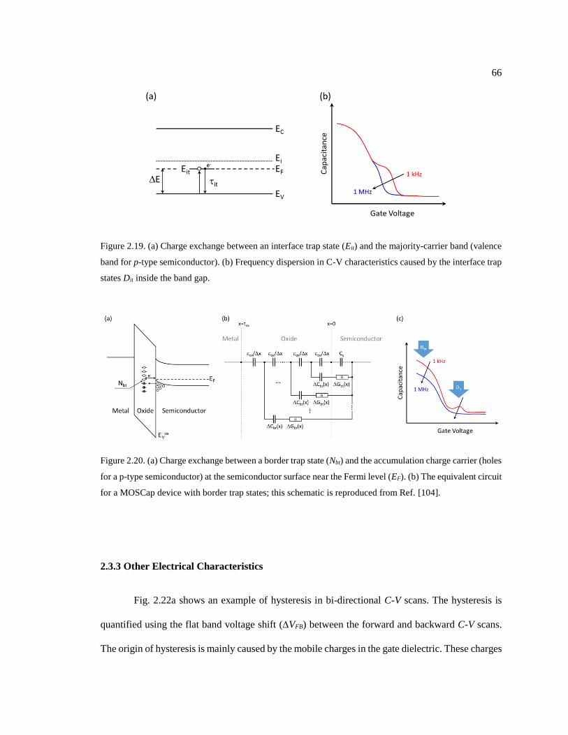
66
Figure 2.19. (a) Charge exchange between an interface trap state (Eit) and the majority-carrier band (valence
band for p-type semiconductor). (b) Frequency dispersion in C-V characteristics caused by the interface trap
states Dit inside the band gap.
Figure 2.20. (a) Charge exchange between a border trap state (Nbt) and the accumulation charge carrier (holes
for a p-type semiconductor) at the semiconductor surface near the Fermi level (EF). (b) The equivalent circuit
for a MOSCap device with border trap states; this schematic is reproduced from Ref. [104].
2.3.3 Other Electrical Characteristics
Fig. 2.22a shows an example of hysteresis in bi-directional C-V scans. The hysteresis is
quantified using the flat band voltage shift (VFB) between the forward and backward C-V scans.
The origin of hysteresis is mainly caused by the mobile charges in the gate dielectric. These charges
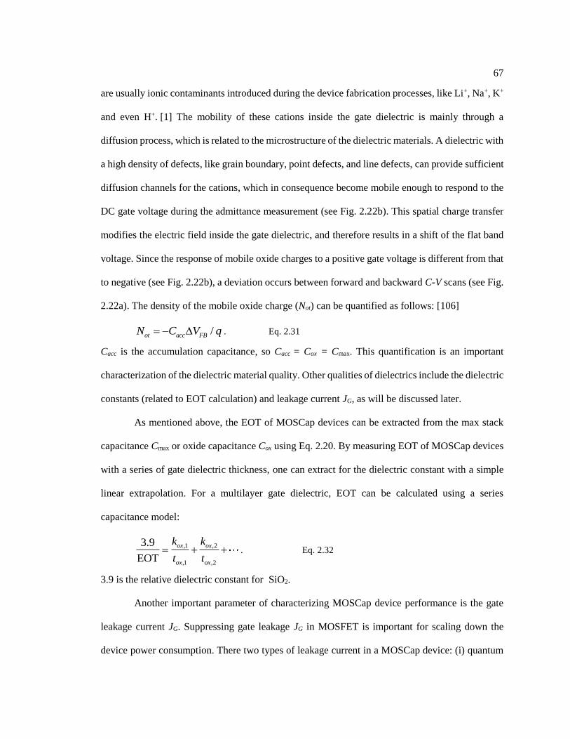
67
are usually ionic contaminants introduced during the device fabrication processes, like Li+, Na+, K+
and even H+. [1] The mobility of these cations inside the gate dielectric is mainly through a
diffusion process, which is related to the microstructure of the dielectric materials. A dielectric with
a high density of defects, like grain boundary, point defects, and line defects, can provide sufficient
diffusion channels for the cations, which in consequence become mobile enough to respond to the
DC gate voltage during the admittance measurement (see Fig. 2.22b). This spatial charge transfer
modifies the electric field inside the gate dielectric, and therefore results in a shift of the flat band
voltage. Since the response of mobile oxide charges to a positive gate voltage is different from that
to negative (see Fig. 2.22b), a deviation occurs between forward and backward C-V scans (see Fig.
2.22a). The density of the mobile oxide charge (Not) can be quantified as follows: [106]
/ot acc FBN C V q . Eq. 2.31
Cacc is the accumulation capacitance, so Cacc = Cox = Cmax. This quantification is an important
characterization of the dielectric material quality. Other qualities of dielectrics include the dielectric
constants (related to EOT calculation) and leakage current JG, as will be discussed later.
As mentioned above, the EOT of MOSCap devices can be extracted from the max stack
capacitance Cmax or oxide capacitance Cox using Eq. 2.20. By measuring EOT of MOSCap devices
with a series of gate dielectric thickness, one can extract for the dielectric constant with a simple
linear extrapolation. For a multilayer gate dielectric, EOT can be calculated using a series
capacitance model:
,1 ,2
,1 ,2
3.9
EOT
ox ox
ox ox
k k
t t . Eq. 2.32
3.9 is the relative dielectric constant for SiO2.
Another important parameter of characterizing MOSCap device performance is the gate
leakage current JG. Suppressing gate leakage JG in MOSFET is important for scaling down the
device power consumption. There two types of leakage current in a MOSCap device: (i) quantum
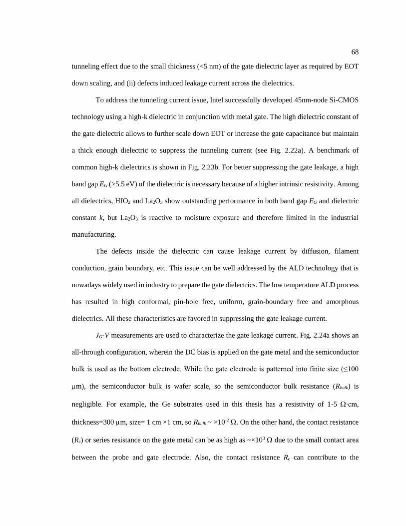
68
tunneling effect due to the small thickness (<5 nm) of the gate dielectric layer as required by EOT
down scaling, and (ii) defects induced leakage current across the dielectrics.
To address the tunneling current issue, Intel successfully developed 45nm-node Si-CMOS
technology using a high-k dielectric in conjunction with metal gate. The high dielectric constant of
the gate dielectric allows to further scale down EOT or increase the gate capacitance but maintain
a thick enough dielectric to suppress the tunneling current (see Fig. 2.22a). A benchmark of
common high-k dielectrics is shown in Fig. 2.23b. For better suppressing the gate leakage, a high
band gap EG (>5.5 eV) of the dielectric is necessary because of a higher intrinsic resistivity. Among
all dielectrics, HfO2 and La2O3 show outstanding performance in both band gap EG and dielectric
constant k, but La2O3 is reactive to moisture exposure and therefore limited in the industrial
manufacturing.
The defects inside the dielectric can cause leakage current by diffusion, filament
conduction, grain boundary, etc. This issue can be well addressed by the ALD technology that is
nowadays widely used in industry to prepare the gate dielectrics. The low temperature ALD process
has resulted in high conformal, pin-hole free, uniform, grain-boundary free and amorphous
dielectrics. All these characteristics are favored in suppressing the gate leakage current.
JG-V measurements are used to characterize the gate leakage current. Fig. 2.24a shows an
all-through configuration, wherein the DC bias is applied on the gate metal and the semiconductor
bulk is used as the bottom electrode. While the gate electrode is patterned into finite size (≤100
m), the semiconductor bulk is wafer scale, so the semiconductor bulk resistance (Rbulk) is
negligible. For example, the Ge substrates used in this thesis has a resistivity of 1-5 ∙cm,
thickness=300 m, size= 1 cm ×1 cm, so Rbulk ~ ×10-2 . On the other hand, the contact resistance
(Rc) or series resistance on the gate metal can be as high as ~×103 due to the small contact area
between the probe and gate electrode. Also, the contact resistance Rc can contribute to the

69
admittance measurement by generating frequency dispersion, due to a similar configuration to a
series RC circuit. [107] To minimize the frequency dispersion, it requires a small contact resistance
RC as follows:
3
22
1
1 1~ ~ 10
2 1 MHz 2 μF/cm 100 μm
C stack
C
stack
R C
RC
. Eq. 2.33
In the gate dielectric, three leakage currents contribute to the transport, the oxide conductance from
the intrinsic properties (Gox), quantum tunneling (Gqt), and defects (Gdf). As mentioned above, Gox
is mainly determined by the band gap EG of the dielectric and is negligible if EG >5.5 eV. The
quantum tunneling effect Gqt can be well addressed by using a thick high-k dielectric. The defect
conductance Gdf is one of the key parameters of the dielectric quality, and is primary target to check
in the JG-V measurement. In the semiconductor surface region, there are two contributions to the
transport, surface conduction GSS and tunneling current Gqt from the semiconductor to the gate
dielectric, while the latter can be ignored compared to the former. Since the electrical properties of
the semiconductor surface is tuned by the gate voltage VG, the surface conductance Gss is variable.
At a depletion or inversion state, either whole or part of the semiconductor surface region is
depleted with a minimized carrier density, so Gss is low and limits the overall conductance. On the
other hand, at an accumulation or inversion state, the semiconductor surface shows a high
conductance, so the JG-V measurement is more representative of the gate dielectrics. In this sense,
the gate leakage current JG at an overdriven voltage (VFB-1 V) is identified to characterize the
transport properties of the gate dielectric in MOSCap.
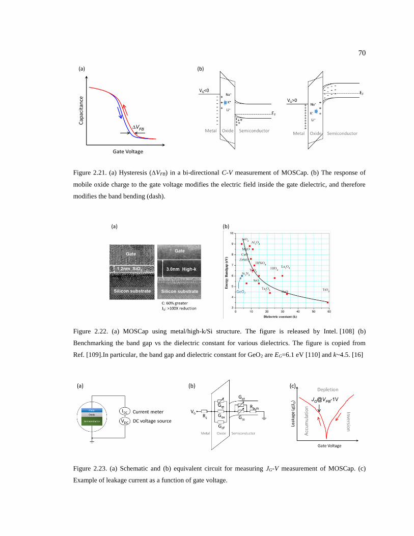
70
Figure 2.21. (a) Hysteresis (VFB) in a bi-directional C-V measurement of MOSCap. (b) The response of
mobile oxide charge to the gate voltage modifies the electric field inside the gate dielectric, and therefore
modifies the band bending (dash).
Figure 2.22. (a) MOSCap using metal/high-k/Si structure. The figure is released by Intel. [108] (b)
Benchmarking the band gap vs the dielectric constant for various dielectrics. The figure is copied from
Ref. [109].In particular, the band gap and dielectric constant for GeO2 are EG=6.1 eV [110] and k~4.5. [16]
Figure 2.23. (a) Schematic and (b) equivalent circuit for measuring JG-V measurement of MOSCap. (c)
Example of leakage current as a function of gate voltage.
71
2.3.4 Data Analysis
This section discusses in details about the data analysis for border trap states. As shown in
the equivalent circuit of Fig. 2.20b, the evolution of the admittance Y for a MOSCap with border
trap states satisfies: [104]
22
2
01
bt
x
ox
j q NdY Y
dx j j e
. Eq. 2.34
x is the depth of the border traps into the gate dielectric. The boundary condition is
0 sY x j C . The first term on the right side of Eq. 2.34 originates from the gate dielectric
capacitance, while the second from the border trap states. Analytical solution for Eq. 2.34 is
extremely complicated, and therefore not applicable in the real data analysis. Instead, numerical
simulations with parameters to be fitted are more straightforward and give relatively reliable
estimation of the border trap state density Nbt.
The ratio between these two terms can be estimated as follows when x = 0+:
222
2 3 2
0 02 2
0
: 1 3 10 1 11
s x xbt
x
ox bt ox
Cj q NYj e j e
j j e q N
. Eq. 2.35
This approximation is using Y(x=0+) jCs, Cs≥100 F/cm2 at accumulation, Nbt~ 4.5e19 cm-3∙eV-
1, and ox=GeO2=60. So the border trap term is a perturbation to the overall admittance. By
substitutingY
j
, Eq. 2.34 can be simplified as follows:
22
2
01
bt
x
ox
q Nd
dx j e
. Eq. 2.36
The boundary condition becomes 0 sx C . At high frequencies, the border trap states are
unable to follow up the AC voltage, namely the border trap term can be neglected, and therefore
Eq. 2.36 can be further simplified as:
72
2
(high frequencies)ox
d
dx
. Eq. 2.37
This is the zeroth order approximation solution of Eq. 2.36 with the following solution:
0
1 1
s oxx
x
C . Eq. 2.38
When x=tox, 0 oxC , which is a simple case of a non-defective MOSCap at accumulation region.
At low frequencies, the response time increases exponentially with the x-position of the border
traps, so those traps far away from the interface are unable to respond to the AC voltage. The
furthest distance of responding traps can be estimated as follows:
02
0 max
ln~ 1 ~ 0.56 nm
2
xe x
. Eq. 2.39
In this approximation, a relatively low AC frequency of 10 kHz and 0~×10-10 sec are used. So an
xmax=1 nm oxide thickness is sufficient for the numerical calculation border trap states, while for
x>1 nm, the evolution of admittance can be described by Eq. 2.37, so
22
2
0
2
0 1 nm, 1
1 nm ,
bt
x
ox
ox
ox
q Ndx
dx j e
dx t
dx
. Eq. 2.40
2.3.5 Hardware Information
In this thesis, electrical measurements were carried out on a Cascade probe station (Summit
11000). The Cascade station has an in-situ camera with a calibrated pixel: distance relation, which
allows to take images of the sample electrodes. The electrode sizes were quantified by processing
the images using ImageJ software. A LCR meter (Hewlett Packard 4285A) was used for measuring
capacitance-voltage (C-V) characteristics; a combination of DC and AC voltage was used, with an

73
AC amplitude of 50 mV and a frequency f=75 kHz-1.5 MHz. A parameter analyzer (Keithley
4200-SCS) was used for measuring leakage-voltage (JG-V) characteristics.
74
2.4 X-ray Photoelectron Spectroscopy
2.4.1 Principles of X-ray Photoelectron Spectroscopy
X-ray photoelectron spectroscopy (XPS) is a surface-sensitive characterization that
quantifies the elemental composition, and chemical states of the elements in materials. An ultrahigh
vacuum (<10-8 Torr) is required for the measurement, so in principle this technology can be applied
to only all solid state materials, but liquids are also possible with a special design of differential
pumping mechanism. [111] The sampling depth by XPS is limited to <10 nm. A deeper
measurement, namely depth profiling, can be realized by combining an in-situ sputtering. A typical
resolution of the elemental analysis (3Li-92U) by XPS is ±5%, while H and He are indistinguishable.
XPS is sensitive to small changes of the chemical states in materials, and therefore provides high
resolution spectra particularly in recognizing the oxidation states in semiconductor devices. A
spatial XPS mapping is possible but with a relatively low resolution (>3 m).
The basic principle of XPS is the photoelectron effect discovered by Heinrich Rudolf Hertz
and later explained by Albert Einstein (see Fig. 2.25a). The incident X-ray photon interacts with
the inner core electrons (K, L, etc.), and the photon energy (h) is transfer to an electron so that the
electron overcomes the binding energy (BE) from the nucleus and becomes free with a kinetic
energy satisfies Einstein’s theory:
-photo-eKE h BE . Eq. 2.41
By detecting the kinetic energy (KE) of the photoelectron and knowing the photon energy,
we can find the binding energy of the electrons of inner cores. Fig. 2.25b shows an example of XPS
survey scan for a GeO2(10 nm)/Ge sample. Multiple peaks for Ge (2p, 3s, 3d, etc.) are identified,
as well as strong signals for O peaks. Note that a small signal for C1s is also observed, which is
originating from the surface organic contamination. Since this carbon contamination is inevitable
75
and its peak position is rather constant with a binding energy of BE=284.8 eV, C1s peak has been
generally used as a reference for correcting the spectrum offset. This offset can be from the XPS
system or the electrostatic potential caused by the surface charging effect on insulating samples.
Figure 2.24. (a) Principles of XPS measurements: interaction between the X-ray photon and inner core
electrons. (b) An XPS survey scan for a GeO2(10 nm)/Ge sample.
2.4.2 Data Analysis
The generated photoelectron intensity from a homogenous material with certain thickness
(z) is expressed as follows (also see Fig. 2.26a):
I n SF z . Eq. 2.42
n is the atomic density of the target element in the material, and SF is the sensitivity factor for the
target element, which is determined by the interaction cross section between the target atom and
photon as well as tooling factors. The sensitivity factor SF is independent of the atomic density n
or the chemical states of the target element. If this thin layer is buried inside the material with
certain depth (z), the emitted photoelectron will be in-elastically scattered by the material when
passing through the z-thick overlayer and become attenuated as follows:
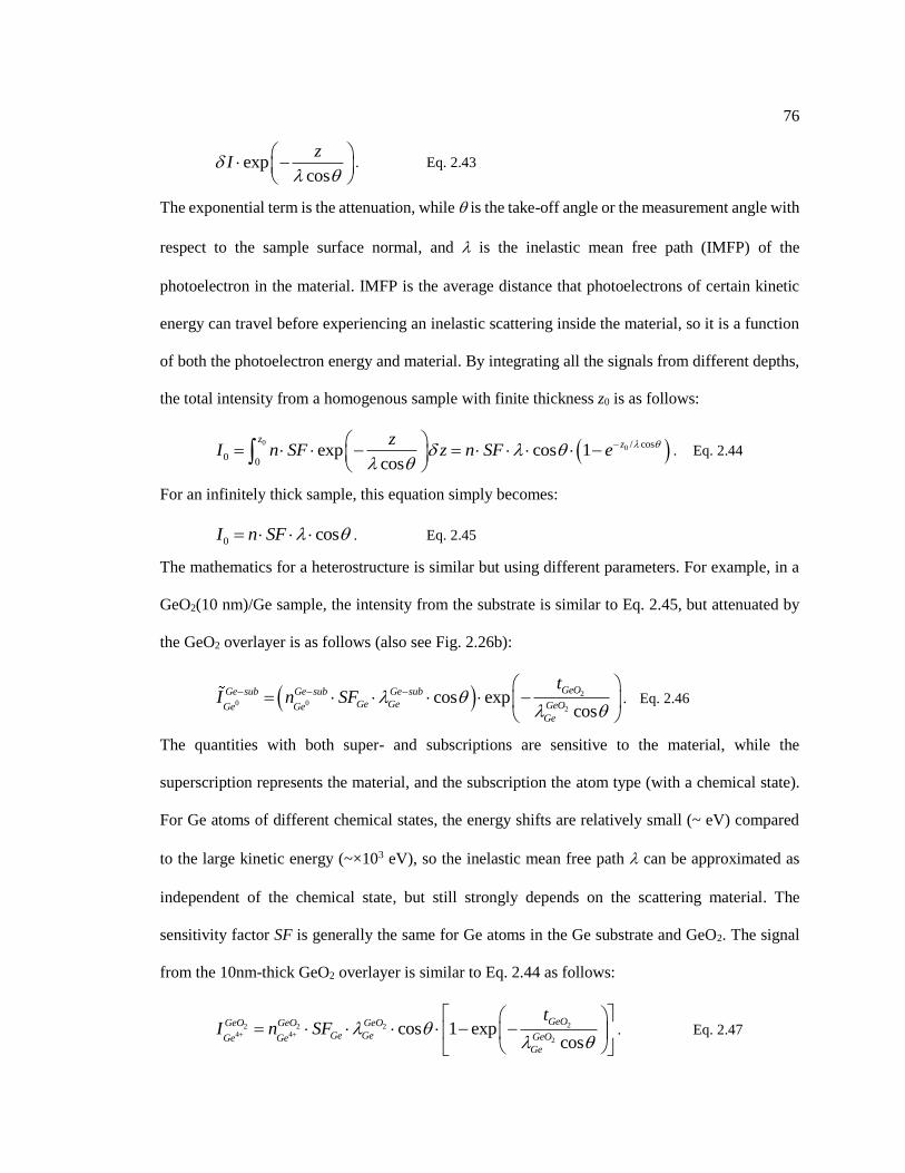
76
expcos
zI
. Eq. 2.43
The exponential term is the attenuation, while is the take-off angle or the measurement angle with
respect to the sample surface normal, and is the inelastic mean free path (IMFP) of the
photoelectron in the material. IMFP is the average distance that photoelectrons of certain kinetic
energy can travel before experiencing an inelastic scattering inside the material, so it is a function
of both the photoelectron energy and material. By integrating all the signals from different depths,
the total intensity from a homogenous sample with finite thickness z0 is as follows:
0
0 / cos
00
exp cos 1cos
zzz
I n SF z n SF e
. Eq. 2.44
For an infinitely thick sample, this equation simply becomes:
0 cosI n SF . Eq. 2.45
The mathematics for a heterostructure is similar but using different parameters. For example, in a
GeO2(10 nm)/Ge sample, the intensity from the substrate is similar to Eq. 2.45, but attenuated by
the GeO2 overlayer is as follows (also see Fig. 2.26b):
2
0 02
cos expcos
GeOGe sub Ge sub Ge sub
Ge Ge GeOGe GeGe
tI n SF
. Eq. 2.46
The quantities with both super- and subscriptions are sensitive to the material, while the
superscription represents the material, and the subscription the atom type (with a chemical state).
For Ge atoms of different chemical states, the energy shifts are relatively small (~ eV) compared
to the large kinetic energy (~×103 eV), so the inelastic mean free path can be approximated as
independent of the chemical state, but still strongly depends on the scattering material. The
sensitivity factor SF is generally the same for Ge atoms in the Ge substrate and GeO2. The signal
from the 10nm-thick GeO2 overlayer is similar to Eq. 2.44 as follows:
22 2 2
4 42
cos 1 expcos
GeOGeO GeO GeO
Ge Ge GeOGe GeGe
tI n SF
. Eq. 2.47

77
So the ratio between the measured signals of Ge4+ and Ge0 can be expressed as:
2 2
224 0
2
: exp 1cos
GeO GeOGeOGeO Ge sub Ge Ge
GeOGe sub Ge subGe GeGe Ge Ge
tnI I
n
. Eq. 2.48
If knowing the take-off angle , density of Ge atoms in Ge substrate and GeO2 ( 0
Ge sub
Gen
, 24
GeO
Gen ) and
the corresponding inelastic mean free paths (Ge sub
Ge , 2GeO
Gen ), we can calculate for the thickness of
GeO2 (2GeOt ). The values for these parameters used in this thesis can found in Tab. 3 and 4.
Fig. 2.27 shows the high resolution XPS spectrum of Ge 3d orbital for the GeO2(10 nm)/Ge
sample with a take-off angle of = 90 °. To quantify the spectrum, a numerical fitting is necessary.
In this thesis, the fitting method is based on Ref. [112–114]. The background of XPS spectra for
Ge 3d is fitting with a Tougaard profile. Each Ge 3d peak is comprised of two sub-peaks,
corresponding to Ge 3d5/2 and Ge 3d3/2, respectively. The sub-peak shapes are described with a
Voigt function with a branch ratio of 0.667. The Ge0 3d5/2 peak is referenced to 29.3 eV. Binding
energy shift for Ge 3d3/2 with respect to Ge 3d5/2 is 0.58eV. The areal ratio between Ge 3d3/2 and
Ge 3d5/2 is fixed at 0.67 which is the ratio of the orbital degeneracy. The core level shifts for +1,
+2, +3, and +4 are 0.8, 1.8, 2.7, 3.3 eV, respectively. A CasaXPS software is used to perform the
numerical fitting.
The numerical fitting of Fig. 2.27 shows that the Ge4+ state dominates in the signal. This is
because the thick GeO2 overlayer strongly attenuates the signal from the underlying Ge substrate.
Plugging the fitted areal ratio between Ge4+ and Ge0 (from the Ge substrate) and the other
parameters from Tab. 3 into Eq. 2.46, the thickness of GeO2 is calculated to be 9.84 nm, which
agrees well with the result of 10.1±0.3 nm given by spectroscopic ellipsometry measurement. So
XPS is a relatively precise method of determining film thickness, especially the native thickness
on semiconductors. When characterizing ultrathin films (tox≤ 3 nm), the signal from the oxide

78
becomes small compared to that of the semiconductor, and therefore may result in large uncertainty
in determining the oxide thickness. To further improve the precision, an angel-resolved XPS
measurement is necessary. From Eq. 2.46, the intensity ratio is sensitive the take-off angle . By
varying the take-off angle from 90 ° to , the effective sampling depth changes by a factor of cos.
By a linear extrapolation, we can obtain a precise thickness of native oxide (see Fig. 2.28). As for
multilayer structures, the principles of data analysis is the same, but much more complicated in
mathematics.
Table 2.5. XPS parameters for Ge3d, O1s and Al2p orbitals used in this work. The calculation of the inelastic
mean free path is performed based on Ref. [115]. The XPS light source is Al K (h= 1486.70 eV).
Orbital RSF BE (eV) KE (eV) IMFP in Ge (Å) IMFP in GeO2 (Å) IMFP in Al2O3 (Å)
Ge3d 0.380 29.3 1457.41 29.92 26.46 33.60
O1s 0.660 530.0 956.71 21.61 19.14 24.32
Al2p 0.185 74.6 1412.11 29.19 25.82 32.78
Table 2.6. Some basic properties of materials used in this work.
Material Density (g/cm3)
Formula density (cm-3)
Monolayer thickness
(Å) Dielectric constant
GeO2 4.25 2.44E+22 3.45 4.5 [16]
AlO1.5 3.00 3.54E+22 3.04 8
HfO2 9.68 2.77E+22 3.31 22
Ge 5.32 4.60E+22 2.79 16
Figure 2.25. (a) XPS signal from a homogenous material. (b) XPS signal from a GeO2(10 nm)/Ge sample.
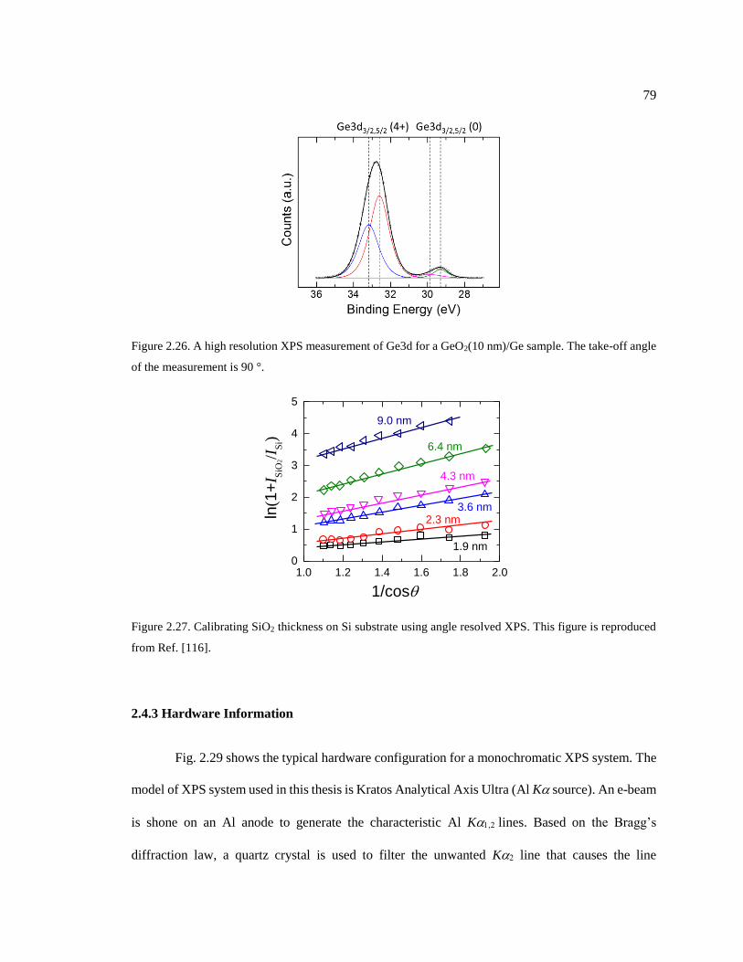
79
Figure 2.26. A high resolution XPS measurement of Ge3d for a GeO2(10 nm)/Ge sample. The take-off angle
of the measurement is 90 °.
Figure 2.27. Calibrating SiO2 thickness on Si substrate using angle resolved XPS. This figure is reproduced
from Ref. [116].
2.4.3 Hardware Information
Fig. 2.29 shows the typical hardware configuration for a monochromatic XPS system. The
model of XPS system used in this thesis is Kratos Analytical Axis Ultra (Al K source). An e-beam
is shone on an Al anode to generate the characteristic Al Klines. Based on the Bragg’s
diffraction law, a quartz crystal is used to filter the unwanted K line that causes the line
1.0 1.2 1.4 1.6 1.8 2.00
1
2
3
4
5
1.9 nm
2.3 nm3.6 nm
4.3 nm
6.4 nm
ln(1
+I S
iO2/I
Si)
1/cos
9.0 nm
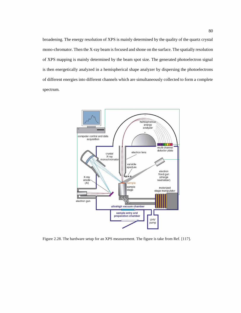
80
broadening. The energy resolution of XPS is mainly determined by the quality of the quartz crystal
mono-chromator. Then the X-ray beam is focused and shone on the surface. The spatially resolution
of XPS mapping is mainly determined by the beam spot size. The generated photoelectron signal
is then energetically analyzed in a hemispherical shape analyzer by dispersing the photoelectrons
of different energies into different channels which are simultaneously collected to form a complete
spectrum.
Figure 2.28. The hardware setup for an XPS measurement. The figure is take from Ref. [117].

Chapter 3
Atomic Layer Deposition of High-k Dielectrics on Germanium
3.1 Introduction
Integrating high-permittivity (high- or high-k) dielectrics on Ge is necessary for utilizing
Ge as the channel material in the CMOS technology, which requires highly downscaled device
dimensions and high carrier mobility. As mentioned above in Chapter 1, the deposition of high-k
dielectrics on Ge, usually performed by atomic layer deposition (ALD) method, is not
straightforward. [10,15] In qualifying the electrical performance of Ge devices, a few factors need
to be under consideration: (i) a high capacitance density from the gate dielectric, which requires an
small thickness and large dielectric constant of the dielectric layer. (ii) Superior qualities of the
dielectric/Ge interface, including a low interface roughness, a low density of electrically active
defect trap states locating in the near-interface semiconductor and the gate dielectrics. (iii) A low
leakage current through the gate dielectrics, which is primarily a characteristic of the quality of the
dielectric itself; defect states in the dielectrics related to the leakage current are created during the
fabrication processes, e.g. unideal initial nucleation and interfacial reaction, etc.
To take into account all the three important factors, a process control metrology is
inevitable. Meanwhile the conjunction with an atomic scale understanding of the mechanism is
beneficial to facilitate the process optimization. This chapter will bring onto the table about how to
use in-situ and ex-situ metrologies to control the fabrication process of Ge MOSCap devices,
entailing in-situ preparing atomically flat and oxygen free Ge surface in Section 3.2, exploring the
surface chemistries of ALD nucleation behaviors on Ge substrates with different surface states in
Section 3.3, and optimizing a gate dielectric stack on Ge with superior electrical characteristics in
82
Section 3.4. The experimental discoveries are compared to ReaxFF simulations from the
collaborators (Prof. Adri van Duin group at Penn State University) for more mechanism details at
an atomic scale. This combinatory approach of experiments and simulations may offer a more
straightforward and rational route in developing Ge-based CMOS technologies in the future
semiconductor manufacturing.
Note that the simulation results were performed by the collaborators from Prof. Adri van
Duin group at Penn State University. In order to give complete explanation of the ALD mechanism,
some of the simulation results are also included in this thesis. Also, note that part of the results in
this chapter have been published in our previous papers, so similar figures, data analysis, and
discussions may be found somewhere else. [35,118]
3.2 Preparing Pristine Ge Surfaces
To ensure the performance of Ge-based transistors, previous researches have pointed out
the key role of the interface between Ge and the gate insulator, which affects the gate leakage
current, capacitance density, sub-threshold characteristics and the effective carrier mobility in the
channel. [119] So it becomes important in the Ge device manufacturing to prepare a pristine Ge
surface with atomic flatness and free of organic contaminants, native oxide, and metal
contaminants, so as to minimize the potential origin of interface defects in the subsequent
semiconductor processing.
Various surface preparation approaches have been successfully developed to remove the
native oxide and organics on Ge, including wet chemical clean, argon ion bombardment and H2
plasma or atomic hydrogen (H*) clean. [119] Compared to other cleaning processes, the H2
plasma [120] or atomic hydrogen (H*) [121] clean appears attractive because it can simultaneously
remove the native oxide and organic contaminations on Ge. Also, it can be performed in-situ at a
83
relatively low temperature (≥180 °C), [122] and does not require an ultra-high-vacuum (UHV)
annealing at high temperatures (>390 °C) to achieve a pristine Ge surface. [119] Because the
relatively low dielectric constants of GeO2 (k~4.5) limits the device scaling, a removal of native
oxide on Ge by H2 plasma is particularly important for developing high-k/Ge transistors. Previous
studies on this issue mainly focused on the effectiveness of removing oxygen from the Ge
surface, [121–125] but rarely discussed the reaction mechanism between the H* radicals and GeO2,
which is essentially important to understand the origin of electrically active defects present at the
dielectric/Ge interface of the transistor devices. As will be shown in this section, the H2 plasma
clean of GeO2 undergoes a distinct reaction scenario at low temperatures compared to that at high
temperatures. The reaction details were examined through the analysis of atomic force microscopy
(AFM) and Raman spectroscopy, and a transition temperature was mapped out between the two
mechanisms.
3.2.1 Experimental details
The installation of an in-situ plasma source on ALD system can be found in Section 2.1.2.
Inside the plasma source, H2 gas mixed with Ar gas is dissociated or ionized by the RF
electromagnetic field inside the induction coil. The majority of the plasma particles are the same
as the initial input flow, with neutral Ar and H2, while a small portion (<10 %) is dissociated or
ionized, forming Ar+, H2+, H+, H-, atomic hydrogen (or H* radicals) and free electrons (see Fig.
3.1). Among all these particles, the H* radicals are believed to be the most reactive in removing the
native oxide on Ge. [125]
GeO2(10 nm)/p-Ge(100) samples were used in this work for studying the H2 plasma clean.
P-Ge(100) substrates (Ga-doping, =1.0-5.0 cm, supplied by Umicore Electro-Optic Materials)
were degreased by acetone/isopropyl-alcohol(IPA), and then rinsed by DI-H2O to remove the
84
surface native oxide. The pre-cleaned Ge substrates were annealed in a muffle furnace in air at 490
°C/2 hrs to grow a GeO2 overlayer, with a thickness of 10.1±0.3 nm determined by spectroscopic
ellipsometry (M-2000U, = 240~1000 nm, J.A. Woollam Co.). Then the GeO2/Ge samples were
loaded into an ALD chamber (ALD-150LX, Kurt J. Lesker Co.) for in-situ H2 plasma treatments
at various temperatures (substrate temperature Tsub= 110-330 °C). The H2 plasma was generated by
a remote radio frequency (RF) plasma source (H2: Ar= 8: 112 sccm, 300 Watts/30 min) with a
background Ar pressure of 1.2 Torr. After the H2 plasma clean, a capping layer of 2 nm Al2O3 was
grown (using tri-methyl-aluminum and H2O as the precursors), to protect the Ge surface from the
air contamination during the sample transfer for further measurements. The chemical states of Ge
were characterized by X-ray photoelectron spectroscopy (XPS, Kratos Analytical Axis Ultra, Al
Ksource). The surface morphology of all samples was measured by atomic force microscopy
(AFM, Bruker Dimension Icon). The vibrational modes of surface Ge was examined by Raman
spectroscopy (=488 nm, 5.0 mWatts, Horiba LabRam).
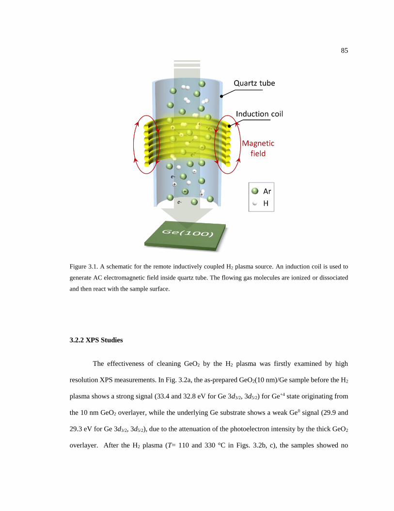
85
Figure 3.1. A schematic for the remote inductively coupled H2 plasma source. An induction coil is used to
generate AC electromagnetic field inside quartz tube. The flowing gas molecules are ionized or dissociated
and then react with the sample surface.
3.2.2 XPS Studies
The effectiveness of cleaning GeO2 by the H2 plasma was firstly examined by high
resolution XPS measurements. In Fig. 3.2a, the as-prepared GeO2(10 nm)/Ge sample before the H2
plasma shows a strong signal (33.4 and 32.8 eV for Ge 3d3/2, 3d5/2) for Ge+4 state originating from
the 10 nm GeO2 overlayer, while the underlying Ge substrate shows a weak Ge0 signal (29.9 and
29.3 eV for Ge 3d3/2, 3d5/2), due to the attenuation of the photoelectron intensity by the thick GeO2
overlayer. After the H2 plasma (T= 110 and 330 °C in Figs. 3.2b, c), the samples showed no
86
observable Ge+4 signal but a strong peak doublet for Ge0, so GeO2 has been effectively removed by
the H2 plasma. [121,124] The weak signal for Ge+1 is attributed to the interfacial transition between
the Al2O3 capping layer and Ge substrate. [35,126]
The driving force of cleaning GeO2 is mainly attributed to the highly reactive atomic
hydrogen (or H* radicals) generated by the plasma source. [120–122,124] As a control experiment,
a simple exposure of GeO2/Ge to a H2 flow with zero plasma power did not result in obvious change
of the GeO2 thickness or the chemical states of Ge (data no shown here). Three reaction routes are
proposed, with the free energy (G) calculations based on Reference [33]:
(I) GeO2(s) + 8H*(g) GeH4(g) + 2H2O(g),
G= -1410 kJ/mol at 400 K and -1328 kJ/mol at 600 K;
(II) GeO2(s) + 4H*(g) Ge(s) + 2H2O(g),
G= -739 kJ/mol at 400 K and -716 kJ/mol at 600 K;
(III) GeO2(s) + 2H*(g) GeO(g) + H2O(g),
G= 120 kJ/mol at 400 K and 86 kJ/mol at 600 K.
While the route (III) is thermodynamically prohibited, (I) and (II) are energetically favored
candidates for the H2 plasma cleaning mechanisms. Comparing (I) and (II), both reactions result in
a removal of O species in the GeO2 layer by releasing volatile H2O and leave no oxidized Ge states
in the samples, so they cannot be distinguished by using only XPS measurements. In the route (I),
the whole GeO2 layer is removed and the underlying Ge bulk is directly exposed, while an overlayer
of elemental Ge is created on the Ge bulk in (II), so the overlayer thickness after the H2 plasma
treatment is an effective indicator to identify the reaction mechanism.

87
Figure 3.2. High resolution XPS measurements of Ge 3d at a 90 ° take-off angle for GeO2(10 nm)/Ge samples
(a) before H2 plasma, (b) after H2 plasma at T=110 °C, and (c) after H2 plasma at T=330 °C. The numerical
deconvolution is based on References [112–114] with a Tougaard background profile. A Voigt profile (0.667
branching ratio) is used to describe all the peak shapes. The Ge0 3d5/2 peak is referenced to 29.3 eV. Binding
energy shift for Ge 3d3/2 with respect to Ge 3d5/2 is 0.58eV, and the areal ratio between Ge 3d3/2 and Ge 3d5/2
is fixed at 0.67. The core level shifts for +1, +2, +3, and +4 are 0.8,1.8,2.7,3.3 eV, respectively.
3.2.3 AFM Studies
A shadow mask method was used to figure out the overlayer thickness after the H2 plasma.
During the plasma exposure, a piece of smooth sapphire substrate (surface roughness Rq=0.1 nm)
was used to partially mask the GeO2/Ge samples (Fig. 3.3a). As a result, a step was created across
the shadowed and un-shadowed regions. After the plasma, no A2lO3 capping was grown and the
samples were directly transferred to the AFM system to measure the step height. Fig. 3.3b shows
the step profile for the GeO2/Ge sample after the H2 plasma at 110 °C. The left side of the step was
shadowed by the sapphire mask, namely made of GeO2, while the right side was cleaned by the H2
plasma. The step height is ~8.48 nm, slightly smaller than the expected height of 10 nm if the whole
GeO2 is completely removed by following the route (I). But this small deviation in the step height

88
can be understood as a result of surface oxidation on the right side of the step by air exposure. A
typical thickness of native GeOx formed by air oxidation on Ge is ~3.06±0.04 nm as measured by
spectroscopic ellipsometry, corresponding to a transformation of ~1.70 nm thick surface Ge layer
into native GeOx. Consequently, the formation of GeOx overlayer on the cleaned Ge side lessens
the overall step height (see the structure schematic in Fig. 3.3b). Regarding this matter, the
theoretical step height was calculated to be 8.74 nm, which is comparable to the experimental result
(Tab. 1). So the route (I) is identified as the reaction mechanism for the H2 plasma clean at 110 °C.
As for the high temperature plasma at 330 °C, however, the measured step height was only ~3.25
nm (Fig. 3.3c), indicating a distinct mechanism. Considering the route (II) as the mechanism and
taking into account the surface oxidation effect (see the structure schematic in Fig. 3.3c), the
theoretical step height becomes 3.14 nm and is comparable with the high temperature result (Tab.
1). So we conclude that at 330 °C, the H2 plasma only reduces GeO2 into elemental Ge by following
the route (II). The absence of GeH4 formation in the route (II) at high temperatures agrees with the
residual gas analysis (RGA) at 300 °C by Schneider et al. [120] Unfortunately, they did not show
the results for lower temperatures.
Another interesting evidence of the temperature dependence of the cleaning mechanism is
the Ge surface roughening induced by the H2 plasma. In-situ spectroscopic ellipsometry (SE) has
been used to real-time monitor the H2 plasma clean on GeO2(~1 nm)/Ge surfaces at various
temperatures (see Fig. 3.4a). At 110 C, H2 plasma can effectively remove the native GeO2, but an
over-exposure resulted in an irreversible increase in the “GeOx” thickness. This increase indicates
that the surface is deviating from pure Ge during the over-exposure of H2 plasma. Ex-situ atomic
force microscopy (AFM) measurement (see Fig. 3.4b) showed that the surface roughness was
significantly increased (root mean square of roughness RMS=0.472 nm), compared to that before
the plasma clean (RMS=0.295 nm). So the ‘GeOx’ thickness increase observed by in-situ SE is the
surface roughness layer, whose optical properties are different from Ge bulk. [127] A similar effect
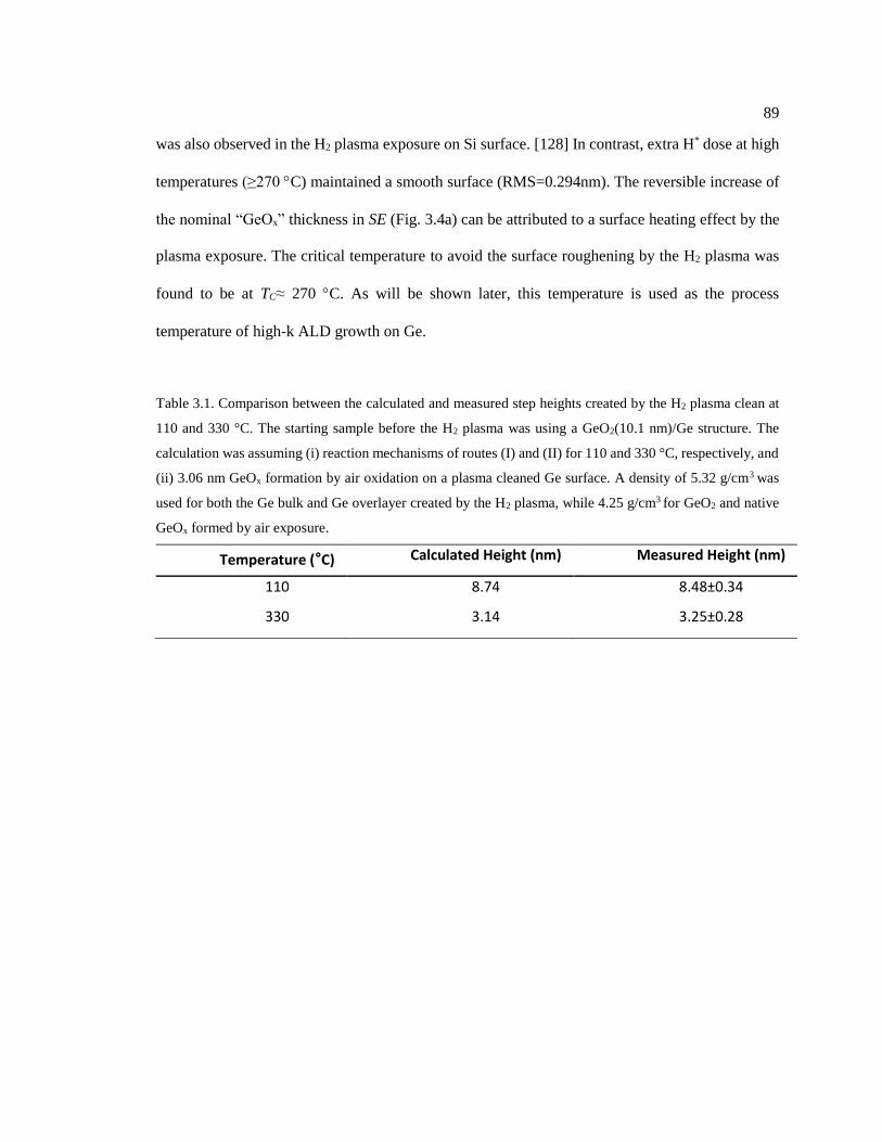
89
was also observed in the H2 plasma exposure on Si surface. [128] In contrast, extra H* dose at high
temperatures (≥270 C) maintained a smooth surface (RMS=0.294nm). The reversible increase of
the nominal “GeOx” thickness in SE (Fig. 3.4a) can be attributed to a surface heating effect by the
plasma exposure. The critical temperature to avoid the surface roughening by the H2 plasma was
found to be at TC≈ 270 C. As will be shown later, this temperature is used as the process
temperature of high-k ALD growth on Ge.
Table 3.1. Comparison between the calculated and measured step heights created by the H2 plasma clean at
110 and 330 °C. The starting sample before the H2 plasma was using a GeO2(10.1 nm)/Ge structure. The
calculation was assuming (i) reaction mechanisms of routes (I) and (II) for 110 and 330 °C, respectively, and
(ii) 3.06 nm GeOx formation by air oxidation on a plasma cleaned Ge surface. A density of 5.32 g/cm3 was
used for both the Ge bulk and Ge overlayer created by the H2 plasma, while 4.25 g/cm3 for GeO2 and native
GeOx formed by air exposure.
Temperature (°C) Calculated Height (nm) Measured Height (nm)
110 8.74 8.48±0.34
330 3.14 3.25±0.28
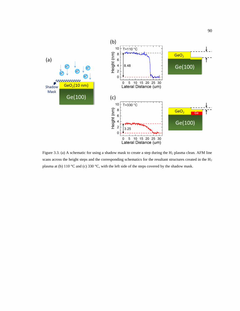
90
Figure 3.3. (a) A schematic for using a shadow mask to create a step during the H2 plasma clean. AFM line
scans across the height steps and the corresponding schematics for the resultant structures created in the H2
plasma at (b) 110 °C and (c) 330 °C, with the left side of the steps covered by the shadow mask.
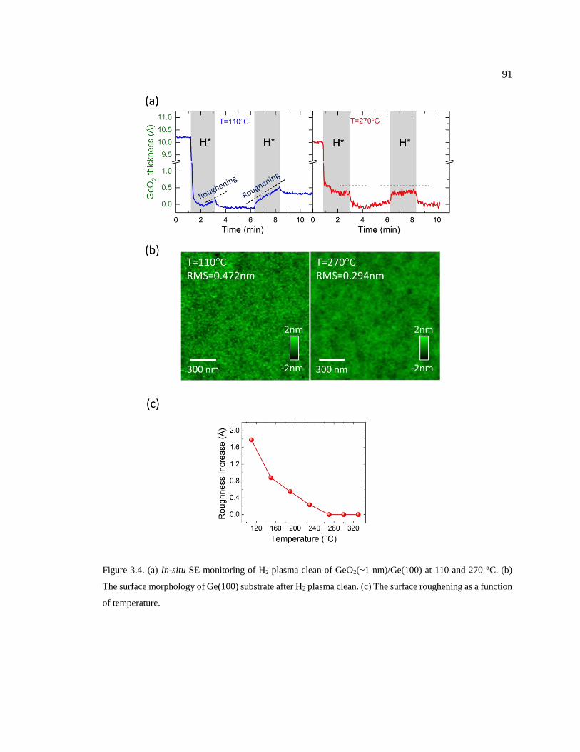
91
Figure 3.4. (a) In-situ SE monitoring of H2 plasma clean of GeO2(~1 nm)/Ge(100) at 110 and 270 °C. (b)
The surface morphology of Ge(100) substrate after H2 plasma clean. (c) The surface roughening as a function
of temperature.
92
3.2.4 Raman Studies
The reaction mechanisms were further examined by Raman spectroscopy. The Raman
spectrum for the as-prepared GeO2(10 nm)/Ge sample (Fig. 3.5a) is an almost identical to that a Ge
substrate right after the acetone/IPA/DI-H2O clean (data not shown here), so the Raman peak (300.9
cm-1, FWHM 2.9 cm-1) is identified as the Ge bulk. [129] The small asymmetry at lower
wavenumbers (~290.9 cm-1) is ascribed to the electronic Raman scattering induced by the free
carriers in the Ge bulk, [130,131] and fitted with a secondary peak labeled as ‘doping’. No Fano
function was used to fit the Ge bulk spectrum because of the relatively low doping level (0.7~3e15
cm-3). After a 100 °C H2 plasma and subsequently capping with an Al2O3 protecting layer, the
Raman spectrum (Fig. 3.5b) is similar to that of the Ge bulk, but with another small and broad peak
(red curve, 296.8 cm-1, FWHM 6.8 cm-1), which is attributed to the defects on the Ge surface
caused by the low-temperature H2 plasma damage [130] and is labeled as ‘poly-Ge’. On the
contrary, the high-temperature H2 plasma treatment (330 °C in Fig. 3.5c) resulted in a significant
intensity of poly-Ge peak. The rise of poly-Ge signal agrees with the above-mentioned reaction
route (II) for the high-temperature H2 plasma. In the route (II), GeO2 is reduced into elemental Ge
and forms an additional overlayer on the Ge bulk. Since an even higher temperature (≥350 °C) is
required to fully crystallize Ge, [132–134] one can expect that this Ge overlayer formed at 330 °C
is nano-polycrystalline and highly defective. This explains the red-shift and peak broadening of the
poly-Ge peak (296.5 cm-1, FWHM 5.9 cm-1) in Fig. 3.5c. [134] Note that the spectral weight of
the doping peak in Fig. 3.5c is also increased significantly, suggesting additional doping source or
charge injection. As reported by J. Cho and R. J. Nemanich, H-induced surface states were absent
after a 300 °C H2 plasma on Ge(100), but the dangling bond states were well identified by angle-
resolved ultraviolet photoemission spectroscopy (ARUPS). [122] Previous studies have showed
that the surface dangling bonds on Ge(100) serve as acceptors or hole injectors by effectively
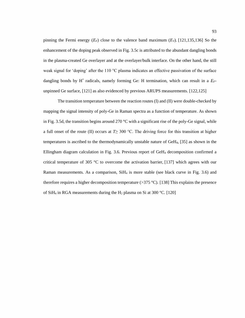
93
pinning the Fermi energy (EF) close to the valence band maximum (EV). [121,135,136] So the
enhancement of the doping peak observed in Fig. 3.5c is attributed to the abundant dangling bonds
in the plasma-created Ge overlayer and at the overlayer/bulk interface. On the other hand, the still
weak signal for ‘doping’ after the 110 °C plasma indicates an effective passivation of the surface
dangling bonds by H* radicals, namely forming Ge: H termination, which can result in a EF-
unpinned Ge surface, [121] as also evidenced by previous ARUPS measurements. [122,125]
The transition temperature between the reaction routes (I) and (II) were double-checked by
mapping the signal intensity of poly-Ge in Raman spectra as a function of temperature. As shown
in Fig. 3.5d, the transition begins around 270 °C with a significant rise of the poly-Ge signal, while
a full onset of the route (II) occurs at T≥ 300 °C. The driving force for this transition at higher
temperatures is ascribed to the thermodynamically unstable nature of GeH4, [35] as shown in the
Ellingham diagram calculation in Fig. 3.6. Previous report of GeH4 decomposition confirmed a
critical temperature of 305 °C to overcome the activation barrier, [137] which agrees with our
Raman measurements. As a comparison, SiH4 is more stable (see black curve in Fig. 3.6) and
therefore requires a higher decomposition temperature (>375 °C). [138] This explains the presence
of SiH4 in RGA measurements during the H2 plasma on Si at 300 °C. [120]
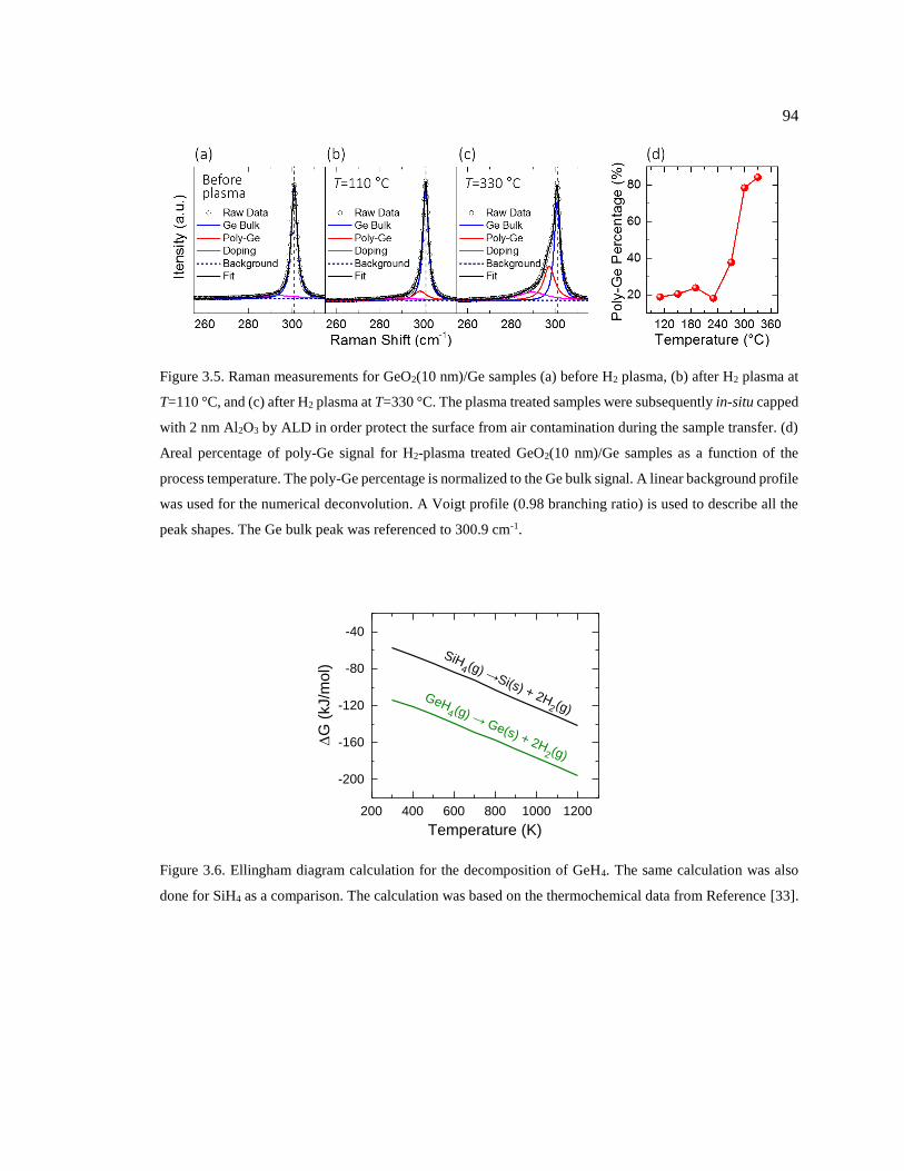
94
Figure 3.5. Raman measurements for GeO2(10 nm)/Ge samples (a) before H2 plasma, (b) after H2 plasma at
T=110 °C, and (c) after H2 plasma at T=330 °C. The plasma treated samples were subsequently in-situ capped
with 2 nm Al2O3 by ALD in order protect the surface from air contamination during the sample transfer. (d)
Areal percentage of poly-Ge signal for H2-plasma treated GeO2(10 nm)/Ge samples as a function of the
process temperature. The poly-Ge percentage is normalized to the Ge bulk signal. A linear background profile
was used for the numerical deconvolution. A Voigt profile (0.98 branching ratio) is used to describe all the
peak shapes. The Ge bulk peak was referenced to 300.9 cm-1.
Figure 3.6. Ellingham diagram calculation for the decomposition of GeH4. The same calculation was also
done for SiH4 as a comparison. The calculation was based on the thermochemical data from Reference [33].
200 400 600 800 1000 1200
-200
-160
-120
-80
-40
SiH4 (g) →Si(s) + 2H
2 (g)GeH
4 (g) → Ge(s) + 2H2 (g)
G
(kJ/m
ol)
Temperature (K)
95
3.2.5 Discussions and summary
The unstable nature of GeH4 can explain the above-mentioned temperature dependence of
the H2 plasma roughening to Ge surfaces. The roughening mechanism at low temperatures is
proposed as: Ge(s) + 4H*(g) GeH4(g). Analogue to Si surface, [139] we believe that the H2
plasma etching of Ge should also show a preference to certain crystallographic orientation ({111}
for Si). This preference results in isotropic removal of surface Ge atoms and therefore a surface
roughening. At high temperatures (≥ 270 °C), the unstable nature of GeH4 inhibits the direct
reaction between H* and Ge, and therefore eliminates the surface roughening. In this sense, the
route (II) mechanism without the GeH4 formation becomes thermodynamically favored than (I).
Regarding the free energy change for both reactions, the route (I) appears more possible than (II),
but this is because of the different initial reaction condition, namely a different H* amount involved.
To equal the initial conditions, extra H* radicals are needed in the route (II) but do not participate
in the reducing reaction with GeO2, so will consequently recombine and form molecular H2 as
follows: 4H* 2H2. Then the route (II) can be rewritten as:
(IV) GeO2(s) + 8H*(g) Ge(s) + 2H2O(g) + 2H2,
G= -1532 kJ/mol at 400 K and -1467 kJ/mol at 600 K.
Overall, the route (IV) after balancing the initial condition is more thermodynamically favored than
(I) at temperatures ≥300 °C, while at low temperatures, the route (IV) is kinetically inhibited.
In summary, the H2 plasma can effectively remove GeO2 on Ge surfaces. However, the low
temperature H2 plasma results in surface roughening, while the high temperature plasma leaves a
defective nanocrystalline Ge overlayer. Neither of these results are favorable for improving Ge
device performances. To address this issue, a combination of wet-chemical clean with a high
temperature H2 plasma is used (see Fig. 3.7). The wet-chemical clean is able most of the organic
contaminants and native oxide, with an ultrathin layer of residual suboxide (<0.5 nm). A 270 °C
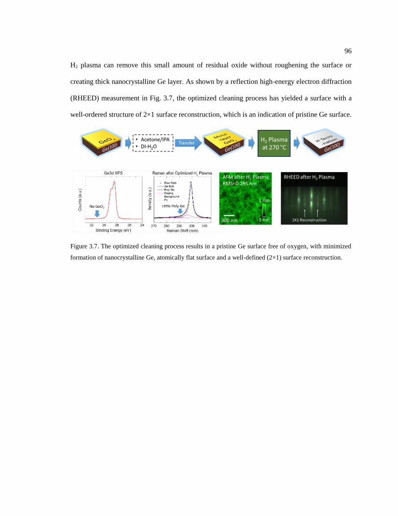
96
H2 plasma can remove this small amount of residual oxide without roughening the surface or
creating thick nanocrystalline Ge layer. As shown by a reflection high-energy electron diffraction
(RHEED) measurement in Fig. 3.7, the optimized cleaning process has yielded a surface with a
well-ordered structure of 2×1 surface reconstruction, which is an indication of pristine Ge surface.
Figure 3.7. The optimized cleaning process results in a pristine Ge surface free of oxygen, with minimized
formation of nanocrystalline Ge, atomically flat surface and a well-defined (2×1) surface reconstruction.
97
3.3 Al2O3 ALD Nucleation Mechanism on Ge
Atomic layer deposition (ALD) has become an important synthesis technique in various
fields of nanotechnology, e.g. semiconductor processing and microelectronics [30,81,140–143],
biomedical applications [144–146] and protective coatings [31,80,147–154]. Considering the large
application space in diverse technological areas it seems surprising that relatively little is known
quantitatively about the kinetic processes in ALD at an atomic level, such as adsorption/desorption,
diffusion, and chemical reactions of molecular species.
When replacing Si with Ge as the new channel materials in CMOS technology, the rapid
pace in the semiconductor industries demands for a better comprehension of ALD processes so as
to master the increasing complexity level and therefore to accelerate optimization cycles. Given
this scenario, the capability of in-situ metrology in conjunction with an atomic scale understanding
of ALD mechanism becomes inevitable. Here, ALD is used to integrate an ultrathin dielectric film
as the gate insulator. The resultant device characteristics are governed by the quality of the
dielectric, but more so by the electrical properties of the dielectric/semiconductor interface.
However, due to the lack of atomic scale understanding of ALD growth kinetics on the
semiconductor surface, the roadmap to obtain highly-scaled and electrically reliable gate stacks is
not straightforward. [30] In case of Ge, it has been found that a direct ALD of high permittivity
(high-k) dielectric on a Ge surface results in poor electrical characteristics dominated by the trap
response formed at the dielectric/semiconductor interface. [17,19,155–158] To address this
challenge, the introduction of an ultrathin interlayer that forms an electrically well behaved
interface with Ge has been proposed. This is layer is thin enough to still allow for competitive
capacitance density scaling and yet thick enough to avoid trap formation through chemical reaction
mechanisms between the high-k and Ge. [159–161] Various materials and deposition conditions
have been applied and resulted in noticeable improvements, but details of the dominant
98
mechanisms for the ALD processes at the atomic scale and how they can be utilized to improve
film nucleation and surface passivation still remain unclear.
In this chapter, a combined experimental and theoretical approach is used to gain insights
into the complex ALD process using in-situ real time spectroscopic ellipsometry (SE) in
conjunction with ReaxFF reactive force field simulations. [162] The ALD deposition kinetics of
Al2O3 on hydrogenated and oxidized Ge surfaces were investigated to quantify the influence of
initial surface chemical states on the reaction kinetics and to relate it to the trap formation during
ALD nucleation. Metal-oxide-semiconductor capacitor (MOSCap) devices were fabricated to
quantify the electrical characteristics of dielectric/Ge interfaces using impedance spectroscopy and
were correlated to the surface chemistry and nucleation mechanism.
3.3.1 Baseline for ALD growth
Before proceeding to the high-k ALD on Ge surface, the baseline of ALD growth needs to
be established. A growth baseline is a parameter set for a standard and optimized ALD process of
certain material, including the growth temperature, precursor dose/purge time, growth rate, optical
and electrical properties of the grown materials, etc. The baseline is particular important when
performing ALD process on a surface that has not been well studied before, because the parameters
from the baseline are good references for the growth of interest that may significantly differ from
the standard growth due to a different surface chemistry. This comparison serves as a good source
of clues for figuring out the nucleation behavior on the unfamiliar surface.
In this thesis, in-situ SE is generally used for real-time monitoring all the processes inside
the ALD chamber, including the ALD growth. The following baseline parameters can be extracted
from the standard ALD growth using in-situ SE:

99
(i) Growth rate or growth per cycle (GPC), which is typically obtained by performing a
long deposition so that the as-obtained thin films are thick enough (> 5nm) for precise thickness
measurement (typical thickness resolution for SE is sub-Angstrom).
(ii) Dielectric functions of the materials 1/2, which are also extracted from the long ALD
deposition; the parameterization of all the ALD grown oxides has been addressed in Section 2.2.3.
(iii) Dose amplitude of metal organic (MO) precursor or adsorption level, which is
represented by the nominal thickness increase measured by SE when MO precursor is dose on the
sample surface; as will be shown later, this quantity is particularly useful for analyzing the initial
nucleation behavior of ALD deposition.
(iii) The ratio between GPC and MO adsorption, which is namely mathematical division
between the two already measured quantities; this ratio is not trivial, because for a standard growth,
the reaction mechanism is well defined, namely the product (i.e. GPC) is proportional to the reactant
(MO dose amplitude); deviation of this ratio from the baseline indicates a new reaction chemistry
present during the ALD growth.
Since Al2O3 is the primary material of interest, detailed baseline has been established for
its ALD growth at T=270 °C (see Fig. 3.8). The baseline ALD of Al2O3 using TMA and H2O is
performed on a Al2O3(30 nm)/SiO2(25 nm)/Si substrate, whose optical properties were well
characterized before the deposition. The baseline growth shows a linear growth mode (see Fig.
3.8a), which is typically observed for a homo-deposition of oxide ALD. The average growth rate
GPC is determined to be 0.86 Å/cycle. Fig. 3.8b shows the details of the ALD growth. Each cycle
starts with a TMA dose, which results in a nominal thickness increase. The fully saturated
amplitude of this increase represents the TMA adsorption level. After purging the residual
unreacted TMA in the chamber with Ar, H2O dose oxidizes the adsorbed TMA into Al2O3, resulting
a smaller drop in thickness. Another Ar purge removes the residual unreacted gas phase H2O. At
the end of the cycle, a net thickness of Al2O3 is grown, which is GPC. The GPC/TMA adsorption

100
ratio is determined to be ~0.404 (see Fig. 3.8c), which on the other hand means the average TMA
adsorption of ~2.13 Å/cycle.
Another useful parameter one can further extract from the above-mentioned baseline
parameters is the density of bonding sites by calculating the areal density of MO adsorption. For
example, to evaluate the bonding site density available for TMA adsorption, we can do the
following calculation: assuming a density of 3.0 g/cm3 for ALD grown Al2O3, [31] then the density
of Al atom is = 3.54×1022 cm-3, areal density of Al atom is 2/3= 1.08×1015 cm-3, and the monolayer
thickness of AlO1.5 is -1/3= 3.04 Å. The baseline GPC of ~0.86 Å corresponds to 0.28 monolayer
of AlO1.5, so an Al areal density of 0.28×2/3=3.05 nm-2 is deposited in each ALD cycle. Since one
TMA molecule contributes one Al atom, the TMA adsorption density= 3.05 nm-2, which is also the
bonding site density available on the sample surface in each cycle.
Figure 3.8. Al2O3 ALD on Al2O3(30 nm)/SiO2(25 nm)/Si. (a) In-situ SE monitoring of real-time thickness.
(b) Enlarged section for Figure (a) with details of the sequential precursor doses, TMA adsorption and GPC.
(c) Extracted ratio of GPC to TMA adsorption as a function of growth cycle. Results published in Ref. [35].
3.3.2 Al2O3 ALD on H-terminated Ge surface
The H-terminated Ge surface (Ge:H) is prepared by exposing the Ge surface to H2 plasma,
as discussed in details in Section 3.1. Even though GeH4 is thermodynamically unstable at 270 °C,
101
a single bonded structure of Ge-Ge-H* can be still allowed to exist to a large extent on a pristine
Ge surface without the defective nanocrystalline Ge, as shown by the Raman spectrum in Fig. 3.7.
A direct Al2O3 ALD on Ge: H surface shows an obvious nucleation delay. The growth
curve measured by in-situ SE is nonlinear (Fig. 3.9a), and the resultant growth rate GPC is gradually
increasing with the ALD cycle number, with an initial growth rate significantly lower than the base
rate for Al2O3 ALD baseline (Fig. 3.9b). The TMA dose rise in initial ALD cycles is weak (red
circles in figure 1c), indicating a difficulty of TMA adsorption on Ge: H. For example, the TMA
adsorption on Ge:H in the very first cycle is only ~17% of the baseline. As mentioned above, the
baseline adsorption density is calculated to be 3.05 nm-2, so in the first cycle, there is only ~0.5/nm2
coverage. The adsorption level approaches the baseline around 25~27th cycle. By comparing the
GPC and the TMA adsorption, we can see that they are relatively proportional to each other (Fig.
3.9c). The large uncertain of the ratio in the initial few cycles is due to the low GPC and TMA
adsorption, which are comparable to the noise level. So we can conclude that the nucleation delay
is mainly caused by the low sticking coefficient of TMA precursor on Ge:H surface. The improved
GPC in later cycles is due to an increased Al2O3 surface coverage through lateral expansion from
initial nucleation sites. Until the surface is fully covered by Al2O3, the growth rate GPC and TMA
adsorption are lining up with the baseline parameters.
AFM measurements of the surface morphology at different ALD stages (Figs. 3.9d-f)
shows that shows that Ge surface is significantly roughened during the nucleation, meaning that
Al2O3 ALD on Ge: H surface is a non-conformal island growth. While the horizontal size of the
islands is hard to estimate due to the relatively low lateral resolution in AFM measurements, the
vertical height can be well distinguished, which is the RMS difference between the Al2O3 fully
covered surface (at 27th cycle) and the starting surface (Ge:H), namely 0.626- 0.294= 0.232 nm,
with a max peak-to-valley difference of ~2.3 nm. Due to this non-conformity, the Al2O3 thickness
102
detected by in-situ SE can be better interpreted as an average of Al2O3 islands and the in-between
voids.
The Al2O3 ALD nucleation delay on Ge: H surface can be supported by our ReaxFF-
nudged elastic band (ReaxFF-NEB) calculations. In Fig. 3.10a, the reaction profile indicates that a
fully hydrogenated Ge surface is chemically inert for TMA precursor due to the high reaction
barrier (Ea~1.41 eV). Also, the H2O adsorption on Ge: H surface is not energetically favorable to
activate the Ge: H surface, namely, the hydroxylation is inhibited (Fig. 3.10b). These two facts
together contribute to the initial nucleation difficulty observed in the experiments.
To figure out the mechanism for initializing TMA chemisorption, additional ReaxFF-NEB
calculations of reaction paths for H diffusion on Ge: H surface, and we found that the formation of
local dangling bonds can serve as the nucleation center. That is, though the ground state is fully
hydrogenated Ge surface, the local dangling bond can form by H-diffusion from the surface into
the interstitial sites in the Ge-sublayer by overcoming a moderate reaction barrier (Ea~0.68 eV; see
Ref. [35] for the reaction profile for H-diffusion into Ge-sublayer) which is feasible at the elevated
temperature in the real experiment (T=270 °C). To demonstrate this, we also performed MD
simulations of H diffusion into Ge-sublayer using H terminated Ge slab (60 Å × 60 Å × 10 Å) with
a vacuum environment (see Fig. 3.11). A density of 0.3 nm-2 for Ge dangling bonds was confirmed
at 800 K, corresponding to ~4.0 % of Ge atoms on the top layer of the H terminated Ge surface. If
assuming TMA will only bond to the Ge dangling bonds, the TMA adsorption site density becomes
0.3 nm-2, which is comparable to the experimental observation of 0.5 nm-2 as mentioned above.
Figs. 3.10c-e shows the ReaxFF-NEB results for the TMA+H2O nucleation on Ge-dangling
bond, which account for effects of the Ge-dangling bond on the TMA chemisorption. In figure 2c,
the TMA precursor energetically favors the local Ge-dangling bond (Ge-*) as following:
Ge-*+ Al(CH3)3 Ge-Al(CH3)3*
Ge-Al(CH3)3*+ Ge-H* Ge-Al(CH3)2*+ CH4+Ge-*
103
The asterisks denote surface species. It is interesting to note that the TMA chemisorption
simultaneously triggers the formation of an additional dangling bond at the neighboring site.
Subsequently, as expected, a H2O dose into the system only hydroxylates the TMA adsorbed site
(Fig. 3.10d, e). The adsorption preference during the above-mentioned TMA and H2O dose was
also confirmed by ReaxFF-MD simulations at 500K (see Supporting Information, TMA and H2O
adsorption on H-terminated Ge surface, for more details). At this stage, there are two available sites
where TMA precursors preferably chemisorb: (1) the newly formed Ge-dangling bond, and (2) the
hydroxylated site [Ge-Al(OH)2*], which originates from the initial local Ge-dangling bond
(Fig.3.10f). As a result, the subsequent Al2O3 ALD nucleates locally around the initial Ge-dangling
bond site, namely, island growth mode.
Two major consequences of the Al2O3 island growth mode on Ge can be expected. First,
the Al-Ge bonds formed in TMA adsorption contribute to the interface trap states in the Ge band
gap. [126] Second, one could expect a high density of boundaries in the Al2O3 layer; [30] these
boundaries act as a leakage channel in the dielectrics. [163] Both consequences imply that a direct
Al2O3 deposition on Ge: H surface yields inferior electrical characteristics of Ge-based devices, as
addressed in our previous paper. [118]
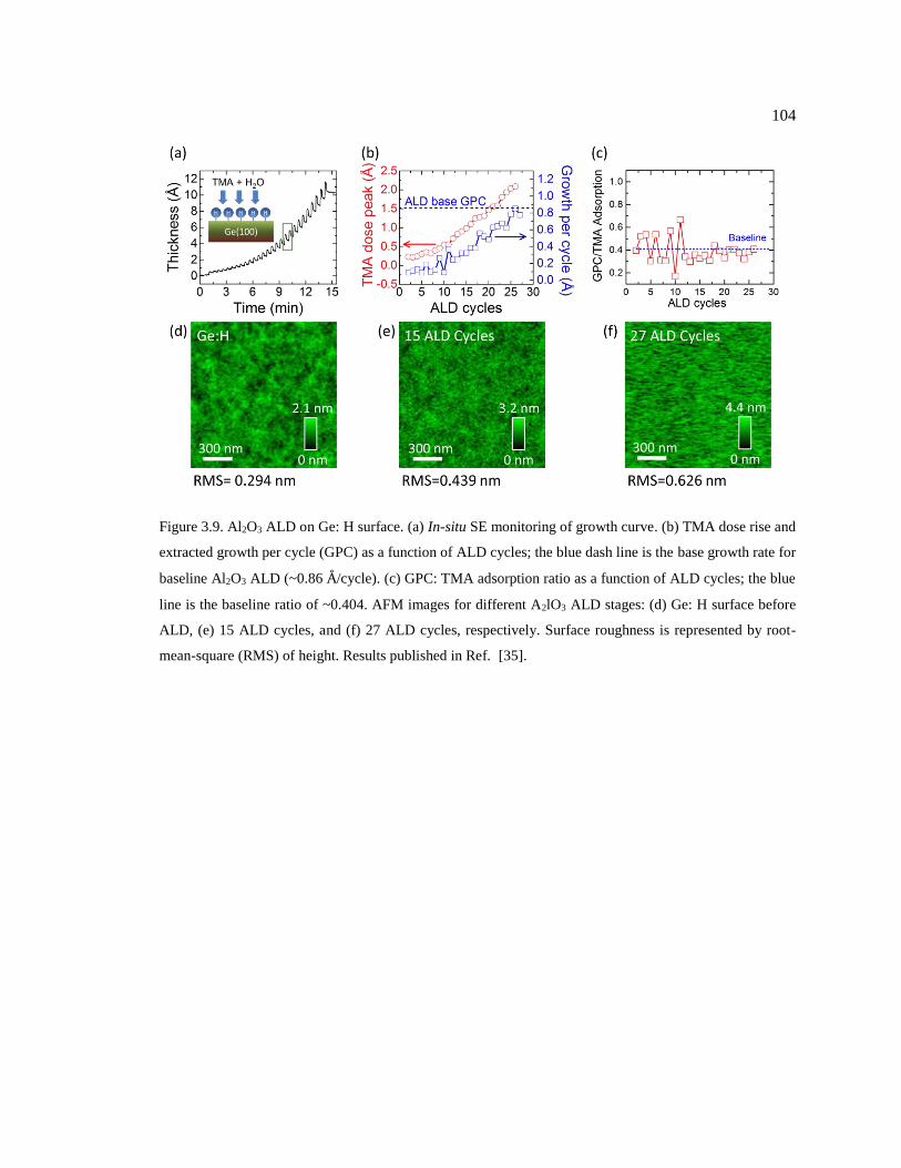
104
Figure 3.9. Al2O3 ALD on Ge: H surface. (a) In-situ SE monitoring of growth curve. (b) TMA dose rise and
extracted growth per cycle (GPC) as a function of ALD cycles; the blue dash line is the base growth rate for
baseline Al2O3 ALD (~0.86 Å/cycle). (c) GPC: TMA adsorption ratio as a function of ALD cycles; the blue
line is the baseline ratio of ~0.404. AFM images for different A2lO3 ALD stages: (d) Ge: H surface before
ALD, (e) 15 ALD cycles, and (f) 27 ALD cycles, respectively. Surface roughness is represented by root-
mean-square (RMS) of height. Results published in Ref. [35].

105
Figure 3.10. Reaction profiles obtained by the ReaxFF-nudged elastic band scheme for Al2O3 ALD on H-
terminated Ge(100). (a) TMA and (b) H2O adsorptions at H-terminated site. (c) TMA adsorption on a Ge-
dangling bond. (d) H2O removes one CH4 group from Ge-Al(CH3)2* site. (e) H2O removes CH4 group from
Ge-Al(CH3)(OH)* site. (f) TMA adsorption at Ge-Al(OH)2* site. The insets correspond to the atomic
structures for the stage at the solid points in each profile, while the neighboring number denotes the
corresponding energy. Results published in Ref. [35].

106
Figure 3.11. Results of MD simulations at 500 K for (a) 80 TMA molecules on a H-terminated Ge(100)
surface with a single Ge-dangling bond; (b) 100 H2O molecules on the H-terminated Ge(100) surface with a
Ge-Al(CH3)2* site. ReaxFF-MD results confirm that TMA and H2O molecules preferably adsorb on the Ge-
dangling and Ge-Al(CH3)2* sites, respectively, rather than H-terminated Ge sites. Results published in
Ref. [35].

107
3.3.3 Al2O3 ALD on oxidized Ge surface
Oxidized Ge surfaces (GeOx/Ge) were obtained by oxidizing Ge:H surfaces prepared by
H2 plasma at 270 °C. Three oxidation modes were evaluated: (i) O2 gas, (ii) continuous O2-plasma
(O*), and (iii) O2 plasma pulses, as shown in Fig. 3.12. Exposing the Ge surface to O2 resulted in a
slow and limited formation of sub-monolayer GeOx (~1 Å) (Fig. 3.12a), while the continuous O2
plasma (Fig. 3.12b) caused rapid Ge oxide formation (~0.7 Å/sec), not suitable for precise control
of the targeted GeOx thickness. A pulsed O2 plasma mode was used (Fig. 3.12c), allowing a precise
adjustment of GeOx thicknesses up to ~5 Å (~1.5 monolayer). The self-limiting behavior was
interpreted as a result of the mild oxidation conditions enabled by the short pulses, suggesting that
the top-most monolayer of GeOx acted as an oxygen protection layer. So the short O2 plasma pulse
mode was used as the optimal preparation process of GeOx/Ge surfaces.
Figure 3.13a shows the in-situ SE monitoring of Al2O3 ALD on GeOx(5 Å)/Ge(100)
surface. The ALD nucleation behavior (Figure 3.13a) is also nonlinear but with distinctively
different characteristics of TMA adsorption and GPC compared to Ge:H surfaces. The nucleation
can be distinguished into four regions. During the first ALD cycle (region I), TMA adsorption is
pronounced, ~45% higher than the baseline; this is attributed to the high density of TMA
chemisorption sites on GeOx. The resultant GPC/TMA-adsorption ratio is significantly higher than
the baseline (Fig. 3.13c) indicating that H2O is not the only oxidizing agent.
In the following five cycles (region II in Fig. 3.13b), the TMA adsorption level is moderate
and relatively constant (~60% of the baseline), but the GPC is close to zero, resulting in a large
deviation of GPC/TMA-adsorption ratio from the baseline (Fig. 3.13c). Even with a sizeable TMA
adsorption, a small Al2O3 overlayer is formed due to intermixing, whereby Al atoms penetrate into
GeOx densifying the oxide. In region III, TMA adsorption level and growth rate gradually approach
the baseline. After ALD cycle n=9 in region IV, all parameters remain relatively constant with

108
values similar to the baseline. At this point, the Al2O3 overlayer coalesces and conventional ALD
Al2O3 process becomes the dominant reaction mechanism
Ex-situ post-deposition characterizations were performed to figure out the mechanism of
Al2O3 ALD on GeOx/Ge. AFM measurement (inset in Fig. 3.13a) reveals that no roughening
occurred during Al2O3 ALD on GeOx/Ge, and therefore excludes the possibility of island growth
mode. The chemical status was examined by X-ray photoelectron spectroscopy (XPS)
measurements (Fig. 3.13d); the samples with Al2O3 ALD on Ge: H and GeOx(3 Å)/Ge(100) serve
as control groups. The deconvoluted peaks for different Ge valent states are shown in Table 3.2.
The first important feature of the XPS results is that the Ge+1 and Ge+2 intensities dominate and
stay relatively constant (<1% change) regardless to the starting surface for Al2O3 ALD. The
equivalent GeOx thickness with Ge+1 and Ge+2 is estimated to be ~4 Å. This sub-oxide layer could
be understood as a transition region from Ge bulk to the oxide overlayer. [126] Second, for Al2O3
ALD on GeOx/Ge surface, Ge+3 and Ge+4 peaks are almost absent, with a sub-angstrom equivalent
thickness. So Ge+3 and Ge+4 have been scavenged during Al2O3 ALD; we call this a TMA self-
clean effect of GeOx. This observation is similar to a previous result reported on Ge by Delabie et
al, [164] and has also been well recognized for TMA [165,166] and Tetrakis (Ethyl-Methyl-
Amino) Hafnium (TEMAH) [167] on III-V semiconductors. The self-clean effect is primarily
driven by thermo-dynamics, wherein Al-O bond is much stronger than Ge-O (see Ellingham
diagram in Fig. 3.14). The electrical consequence of the self-clean effect will be discussed later.
In order to further explore the nucleation mechanism, ReaxFF MD simulations were also
performed for Al2O3 ALD on GeOx/Ge(100), as shown in Fig. 3.15a. The adsorption in the first
TMA is obvious and non-local, creating a TMA overlayer directly bonded to O atoms in GeOx; this
is because the TMA adsorption on GeOx surface has no reaction barrier and is highly exothermic
(-3.02eV; see Fig. 3.15b). Note that part of –CH3 groups already desorb from the surface and form
methane (CH4), and ethane (H3C-CH3) (as highlighted in Fig. 3.15a), so the TMA is partially
109
oxidized by GeOx during adsorption, or in other words, the GeOx is partially reduced, as revealed
in figure 4c. This well explains the abnormal high growth/dose ratio observed in the 1st Al2O3 ALD
cycle on GeOx/Ge (region-I in Fig. 3.13b). Subsequently, the 2nd TMA dose results in little
adsorption and slight change in the chemical state of GeOx, meaning that the surface is somewhat
saturated. Note that the more Al atoms diffuse into GeOx layer due to a longer time frame. The
subsequent H2O dose hydroxylates the adsorbed TMA; during this stage, the Al diffusion into GeOx
layer continues, leading to an intermixture of [AlOx/GeOx]. The statistics of the simulation results
show that the O-atoms in AlOx mainly originate from GeOx (Fig. 3.15d). From this scenario, the
counter-intuitive observation of decent TMA dose but low growth in region-II of Fig. 3.13b can be
understood as a result of intermixing effect, wherein a strong TMA adsorption occurs but little
thickness is accumulated. The following region-III in figure 3b is when the intermixing saturates
and transits to the coalesced Al2O3 ALD in region-IV. Based on the results of ReaxFF MD
simulations, we confirm that GeOx surface is chemically active for TMA+H2O nucleation and
therefore leads to a conformal ALD, in accordance with the above-mentioned AFM study.
In order to evaluate the interface properties, more ReaxFF simulations were performed
about the [AlOx/GeOx]/Ge structure. Fig. 3.16 shows ReaxFF-MD simulations for the thermo-
stability of GeOx/Ge (100) and [Al2O3/GeOx]/Ge (100) interfaces. In the case of GeOx/Ge(100), a
large portion of oxygen atoms diffuses from GeOx layer into Ge subsurface, indicating the thermo-
dynamically unstable nature of GeOx/Ge interface. In contrast, the oxygen diffusion is significantly
suppressed by the existence of Al2O3 layer on GeOx/Ge surface, so the dielectric/Ge interface is
stabilized. Similar stabilization effect has been observed by incorporating other metal or nitrogen
atom into GeO2. [10] Since [Al2O3/GeOx] can form a stable and high quality interface with Ge, we
can use it as the interlayer between the high-k and Ge for device applications. More details about
the fabrication and electrical performance will be discussed later.

110
Table 3.2. De-convoluted peak areas of XPS measurements for samples after Al2O3 ALD on Ge: H, GeOx(3
Å)/Ge(100), and GeOx(5 Å)/Ge(100), respectively. The peak area is normalized by the area sum of Ge0 3d3/2
and Ge0 3d5/2. Results published in Ref. [35].
Starting Surface Ge1+ Ge2+ Ge3+ Ge4+
Ge: H 8.4% 5.1% 0.0% 0.0%
GeOx(3Å)/Ge 8.6% 4.6% 0.4% 0.8%
GeOx(5Å)/Ge 8.7% 4.2% 2.4% 1.2%
Figure 3.12. In-situ SE monitoring for three GeOx growth modes at 270 C: (a) molecular O2 (pO2≈33
mTorr/2min), (b) continuous O*-plasma (8 sec), and (c) sequence of O*-plasma pulses (1.75 sec/pulse). Note
the shorter time scale in (b). Results published in Ref. [118].

111
Figure 3.13. (a) In-situ SE monitoring for Al2O3 ALD on GeOx(5 Å)/Ge(100). Inset is the AFM image right
after Al2O3 ALD; RMS=0.285 nm. (b) TMA dose rise and extracted GPC as a function of ALD cycles; the
ALD base GPC (blue dashi line) is ~0.86 Å/cycle. (c) Al2O3-growth/TMA-dose ratio extracted from
ellipsometry; the blue line of 0.4 is the typical value for Al2O3 ALD. (d) XPS measurements (Ge 3d at 90 °
take-off angle) after 1 nm Al2O3 ALD on different starting surfaces, Ge: H, GeOx(3 Å)/Ge(100), and GeOx(5
Å)/Ge(100), respectively. Inset is the XPS measurements at 15 ° take-off angle. Results published in
Ref. [35].

112
Figure 3.14. Ellingham calculations for As2O3, GeO2, Ga2O3 and Al2O3, respectively. Results published in
Ref. [35].
Figure 3.15. ReaxFF-MD simulations of Al2O3 ALD using TMA+H2O dose on GeOx(5Å)/Ge(100) surface
at 1000 K. (a) Final snapshots of MD simulations for the sequential precursor dose; the MD-NVT simulations
were performed for each dose up to 500 ps; the highlighted molecules 1 and 2 are byproducts of methane
(CH4) and ethane (H3C-CH3), respectively. (b) ReaxFF-NEB scheme for TMA adsorption on GeOx/Ge
surface. (c) Number of oxygen atoms coordinated to Ge during Al2O3 ALD. (d) Oxygen origin of Al2O3
grown on GeOx/Ge surface after Al2O3 ALD. Results published in Ref. [35].
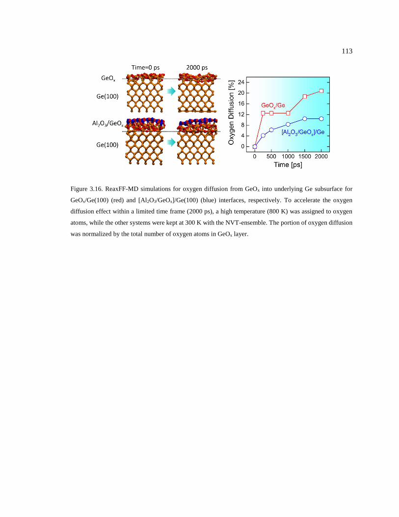
113
Figure 3.16. ReaxFF-MD simulations for oxygen diffusion from GeOx into underlying Ge subsurface for
GeOx/Ge(100) (red) and [Al2O3/GeOx]/Ge(100) (blue) interfaces, respectively. To accelerate the oxygen
diffusion effect within a limited time frame (2000 ps), a high temperature (800 K) was assigned to oxygen
atoms, while the other systems were kept at 300 K with the NVT-ensemble. The portion of oxygen diffusion
was normalized by the total number of oxygen atoms in GeOx layer.
114
3.4. Electrical characterization of Ge MOSCap devices
From the discussions above, the [Al2O3/GeOx] intermixing layer can serve as an electrically
superior interlayer between high-k dielectric and Ge surface. In the real application in device
fabrications, the other electrical performances should also be taken into account, including the
capacitance density or EOT, gate leakage current, and device reliability. So instead of material
engineering, the next step is to engineer the structure of devices. For this purpose, Ge MOSCap
devices can well serve for this purpose, with a structure shown in Fig. 3.17. It is namely a trilayer
dielectric stack using [Al2O3/GeOx] as the interlayer and HfO2 as the high-k dielectric. While the
preparation of a pristine Ge surface has been well addressed in Section 3.1, the fabrication of the
depositing dielectrics and the resultant electrical characteristics will be addressed in this section.
Fig 3.18 shows an overview of the p-Ge MOSCAPs process flow using HfO2/Al2O3/GeOx
gate stacks. Details of the optimization of individual process steps will be discussed further below.
First, p-Ge(100) substrates (Ga-doped, resistivity=1.0-5.0 /cm, by Umicore Electro-Optic
Materials) were degreased with acetone, isopropyl-alcohol and de-ionized water rinses. The
substrates were immediately transferred into the load-lock of ALD system (Kurt J. Lesker
Company ALD-150LX). The following process steps in ALD chamber were monitored by in-situ
SE (M-2000U, J. A. Woollam), which monitors the dielectric function of samples, providing real-
time information of surface modification like deposition and etching. Figs. 3.18a-d show an
example of in-situ SE monitoring the trilayer gate stack development (270 C, background pAr=1.2-
1.5 Torr). The residual native GeOx was effectively removed by in-situ RF atomic hydrogen (H*)
plasma (100 W, H2: Ar=3: 117 sccm, 30 sec), as shown in Figs. 3.18a. The GeOx passivation layer
was grown by oxygen (O*) plasma pulses (125 W, 1.75 sec/pulse, O2:Ar=3:117 sccm) Figs. 3.17b.
The Al2O3 layer was deposited by thermal ALD with tri-methyl-aluminum (TMA) and H2O Figs.
3.18b. The HfO2 layer was deposited by thermal ALD using tetrakis-dimethyl-amino-hafnium
115
(TDMAH) and H2O Figs. 3.18c. Each layer thickness in the trilayer gate stacks was precisely
controlled by in-situ SE. 60nm Ni was thermally evaporated as the gate metal on the samples, which
were then annealed in forming gas (FGA, H2:Ar=20: 1050 sccm, 330 C/10 min).
Equipped with the precise thickness information for each dielectric layer from in-situ SE,
we investigated their effects on the electrical properties of HfO2/Al2O3/GeOx MOSCAPs. The role
of GeOx was first investigated using p-Ge MOSCAPs of HfO2(24 Å)/Al2O3(10 Å)/GeOx stack with
various GeOx thicknesses. The C-V characteristics in Fig. 3.18 show that the sample with ~5 Å
GeOx passivation showed a small frequency dispersion in accumulation (C/Cmax=2.3%),
indicating an improved D-S interface quality (Dit@Ev≈5.11012 cm-2eV-1), while an insufficient
GeOx passivation (0.0 and 2.5 Å) resulted in not only a larger frequency dispersion at accumulation,
but also a higher gate leakage (JG) Fig. 3.19. Thus, we concluded that a minimum GeOx thickness
of ~5 Å was necessary to create a high-quality interface and to maintain a low gate leakage. The
physical mechanism behind this is attributed to that the GeOx passivation increased the conformity
of Al2O3 ALD nucleation (AFM results not shown here), and therefore formed a better quality of
the dielectric-Ge interface and reduced defects in the dielectrics.
The effectiveness of the Al2O3 to stabilize the interface was also studied by electrical
measurement. Figure 3.20 shows the C-V characteristics for HfO2(24 Å)/Al2O3/GeOx(5 Å) gate
stacks with various Al2O3 thicknesses or ALD cycles. As expected, a direct contact between HfO2
and GeOx resulted in an inferior dielectric/Ge interface (Fig. 3.20a); the HfO2/GeOx intermixing
may result in Hf-Ge bond formation [126], contributing to the interface and border trap
states [27,126]. In contrast, a use of 9 cycles ~5 Å Al2O3 deposition well preserved the GeOx/Ge
interface quality (Fig. 3.20c), while no further improvement was found for thicker Al2O3 (~10 Å
for 15 cycles in Fig. 3.20d). Another consequence of introducing Al2O3 stabilization is the
suppression of gate leakage (JG-V in Fig. 3.20e), attributed to the suppression of HfO2/GeOx
intermixing and therefore the reduction of electrically active defects in HfO2 [27,161].

116
The MOSCap device performances were further evaluated by the following electrical
parameters: capacitance density at accumulation (Cmax), C-V hysteresis (VFB), leakage current (JG)
at 1V overdrive, and interface trap density (Dit) at valence band top (Ev) (see Figs. 21a-e). Trends
in the electrical characteristics correlate well with the 4-stage nucleation scenario of Al2O3 ALD on
GeOx/Ge. Cmax directly reflects the capacitance density of the gate oxide and is determined as Cmax=
ox/tox, where ox and tox are the dielectric constant and thickness of the gate oxide layer, respectively.
Instead of n=0 (no Al2O3), Cmax is the highest in n=9 device. An insufficient Al2O3 ALD (n=0, 4)
will result in a direct contact between the subsequently deposited HfO2 and the unstable GeOx/Ge
interface, which has been reported to form volatile GeO diffusing into HfO2 and to oxidize Ge
sublayers via a two-step reaction mechanism. [10] The additional GeOx formed increases the
overall tox and lowers the effective ox of the gate oxide due to a lower ox of GeOx (~4.5), compared
to Al2O3 (~9) and HfO2 (~18), leading to Cmax reduction. For n=9 cycles, intermixing of
[Al2O3/GeOx] is maximized and the Al2O3 overlayer is coalesced, preventing a direct contact
between GeOx/Ge and HfO2. Due to the intermixing, Al2O3 ALD results in a small tox increase and
the resultant densification of the dielectric slightly increases the effective ox; [168] both factors
contribute to a higher Cmax for n=9 compared to n=0, 4. An overgrowth of Al2O3 ALD (n=15) only
causes additional Al2O3 thickness to the overall tox, leading to a decreased Cmax compared to n=9.
Figure 3.17. A structural schematic for a MOSCap device using [Al2O3/GeOx] as the interlayer between high-
k and Ge.
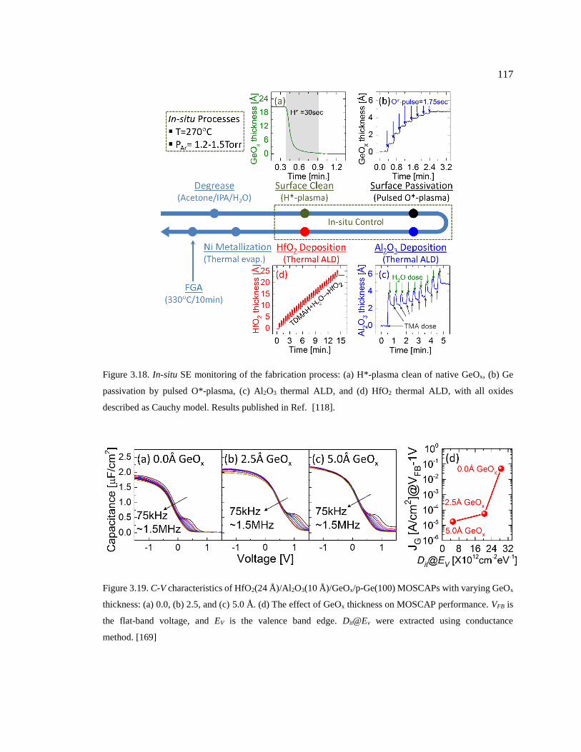
117
Figure 3.18. In-situ SE monitoring of the fabrication process: (a) H*-plasma clean of native GeOx, (b) Ge
passivation by pulsed O*-plasma, (c) Al2O3 thermal ALD, and (d) HfO2 thermal ALD, with all oxides
described as Cauchy model. Results published in Ref. [118].
Figure 3.19. C-V characteristics of HfO2(24 Å)/Al2O3(10 Å)/GeOx/p-Ge(100) MOSCAPs with varying GeOx
thickness: (a) 0.0, (b) 2.5, and (c) 5.0 Å. (d) The effect of GeOx thickness on MOSCAP performance. VFB is
the flat-band voltage, and EV is the valence band edge. Dit@Ev were extracted using conductance
method. [169]
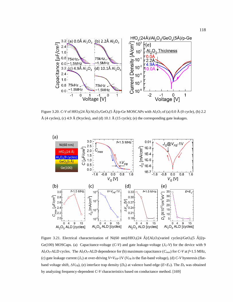
118
Figure 3.20. C-V of HfO2(24 Å)/Al2O3/GeOx(5 Å)/p-Ge MOSCAPs with Al2O3 of (a) 0.0 Å (0 cycle), (b) 2.2
Å (4 cycles), (c) 4.9 Å (9cycles), and (d) 10.1 Å (15 cycle); (e) the corresponding gate leakages.
Figure 3.21. Electrical characterization of Ni(60 nm)/HfO2(24 Å)/[Al2O3(varied cycles)/GeOx(5 Å)]/p-
Ge(100) MOSCaps. (a) Capacitance-voltage (C-V) and gate leakage-voltage (JG-V) for the device with 9
Al2O3-ALD cycles. The Al2O3-ALD dependence for (b) maximum capacitance (Cmax) for C-V at f=1.5 MHz,
(c) gate leakage current (JG) at over-driving V=VFB-1V (VFB is the flat-band voltage), (d) C-V hysteresis (flat-
band voltage shift, VFB), (e) interface trap density (Dit) at valence band edge (E=EV). The Dit was obtained
by analyzing frequency-dependent C-V characteristics based on conductance method. [169]

119
3.5 Summary
A pristine Ge surface that is free of oxygen/organics and atomically flat has been obtained
by combining an ex-situ wet-chemical clean and H2 plasma treatment. The H2 plasma clean process
was found temperature dependent, while high temperatures (≥ 270 °C) are preferred for obtaining
a smooth Ge surface. The Al2O3 ALD nucleation kinetics on hydrogenated and oxidized Ge
surfaces have been investigated in atomic scale by combining in-situ spectroscopic ellipsometry
monitoring and the ReaxFF-MD simulations; the resultant dielectric/semiconductor interface
properties were discussed. The Al2O3 ALD on hydrogenated Ge surface showed an island growth
mode, resulting in defective dielectric/semiconductor interface. A TMA self-clean effect of GeOx
was discovered during the Al2O3 ALD on GeOx/Ge. Both experiments and simulations showed that
the self-clean effect can result in a chemical reduction of GeOx and simultaneously an intermixing
between Al2O3 and GeOx. The [Al2O3/GeOx] intermixing layer was found electrically superior on
Ge; the resultant Ge-MOSCap devices showed improved C-V characteristics and a reduced gate
leakage current. These superior properties were well addressed by the ReaxFF-MD simulations,
which showed that the incorporation of Al2O3 into GeOx can effectively suppress the O-diffusion
from GeOx to Ge subsurface, and therefore stabilize the dielectric/Ge interface properties and
reduce the defects in the dielectrics. By using the [Al2O3/GeOx] intermixing layer as the interlayer
between the high-k and Ge, Ge MOSCap devices with improved electrical performances have been
achieved, with a highly scaled sub-nm EOT (~0.85 nm) and low gate leakage (JG=0.15 mA/cm2 at
VFB-1V) in p-Ge MOSCAP using the trilayer gate stack of HfO2(24 Å)/Al2O3(5 Å)/GeOx(5 Å). The
results are compared to the other reports on Ge MOSCap devices, as shown in Fig. 3.22.
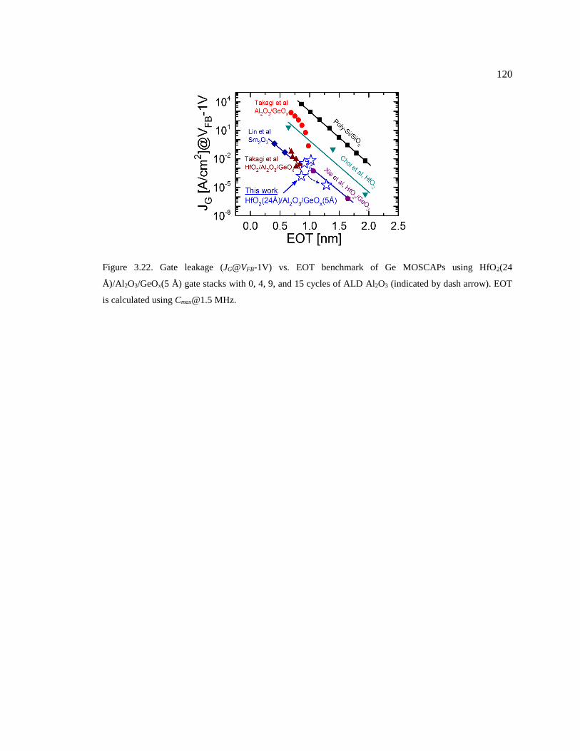
120
Figure 3.22. Gate leakage (JG@VFB-1V) vs. EOT benchmark of Ge MOSCAPs using HfO2(24
Å)/Al2O3/GeOx(5 Å) gate stacks with 0, 4, 9, and 15 cycles of ALD Al2O3 (indicated by dash arrow). EOT
is calculated using [email protected] MHz.

Chapter 4
Atomic Layer Deposition Synthesis of 1T-TaS2
4.1 Introduction
A key challenge of applying 1T-TaS2 as the channels of CMOS devices is preparing wafer
scale thin films so that it is easier for the semiconductor industries to accommodate this new
material into the well-developed VLSI technologies. From the manufacturing point of view, a
mechanical exfoliation to obtain ultrathin layers is inefficient and unreliable, and cannot meet the
requirement of large scale integration. So a direct growth of wafer scale is becoming important.
For this purpose, atomic layer deposition (ALD) provides a possible solution. Compared to other
methods like mechanical exfoliation [54] and chemical vapor deposition (CVD), [74] ALD has not
been widely studied yet.
This chapter will discuss about a direct ALD synthesis of 1T-TaS2 thin films using TaCl5
and H2S as the precursor in a home-built ALD system. Various ALD conditions have been used to
improve the grown material qualities, including the substrate effect, precursor dosage, and growth
temperature. The physical properties of the as-obtained thin film materials were evaluated primarily
using atomic force microscopy (AFM) and Raman spectroscopy. A possible nucleation mechanism
was proposed for explaining the ALD kinetics.
Also, this chapter includes some experimental results about developing a process for ALD
synthesis of ferroelectric HfO2, which is intended to be a gate dielectric required for the future
fabrication of 1T-TaS2 based ferroelectric field-effect transistors (FeFET). The material properties
were evaluated by X-ray photoelectron spectroscopy and electrical polarization measurements.

122
4.2 ALD Growth of 1T-TaS2
4.2.1 Experimental details
A home-built ALD system was used to grow 1T-TaS2 thin films. The details about the
hardware setup has been introduced in Section 2.1.3. An in-situ quartz crystal microbalance (QCM)
metrology has been used to real-time monitor the growth kinetics and optimize the growth
parameters. The foundation of QCM is the high-Q shear-mode piezoelectric effect. The deposited
areal mass results in a small shift of the resonant frequency, as shown in Fig. 4.1. In this thesis, the
density of the material deposited was not calibrated, so instead of directly obtaining thickness
information, the ALD growth monitoring was done through checking the mass change, or even
more conveniently, the frequency shift f.
In this thesis, Si substrates with surface native oxide (~2 nm SiO2) and c-plane sapphire (c-
Al2O3) have been used as the substrates with a size of 10×10 mm2. While the Si substrates were
simply cleaned by acetone/IPA/DI-H2O sonication, the cleaning process for the sapphire substrates
involved more treatments (see Fig. 4.2); in particular, the Nanostrip rinse was intended to
thoroughly remove the organic contaminations. The cleaned substrates were immediately
transferred into the ALD chamber, which was then pumped down to the baseline pressure of ~50
mTorr by a roughing pump. Thereafter, an Ar gas flow was established to sustain a pressure of
~1.03 Torr (more details can be found in Section 2.1.3) and the power of all heaters was switched
on. The ALD growth was performed after all the heating zones of the ALD system were stabilized
in temperature.
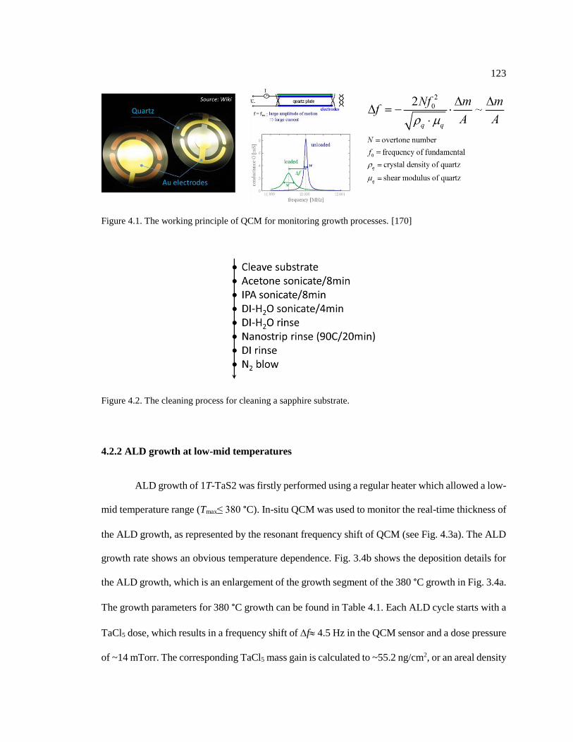
123
Figure 4.1. The working principle of QCM for monitoring growth processes. [170]
Figure 4.2. The cleaning process for cleaning a sapphire substrate.
4.2.2 ALD growth at low-mid temperatures
ALD growth of 1T-TaS2 was firstly performed using a regular heater which allowed a low-
mid temperature range (Tmax≤ 380 °C). In-situ QCM was used to monitor the real-time thickness of
the ALD growth, as represented by the resonant frequency shift of QCM (see Fig. 4.3a). The ALD
growth rate shows an obvious temperature dependence. Fig. 3.4b shows the deposition details for
the ALD growth, which is an enlargement of the growth segment of the 380 °C growth in Fig. 3.4a.
The growth parameters for 380 °C growth can be found in Table 4.1. Each ALD cycle starts with a
TaCl5 dose, which results in a frequency shift of f 4.5 Hz in the QCM sensor and a dose pressure
of ~14 mTorr. The corresponding TaCl5 mass gain is calculated to ~55.2 ng/cm2, or an areal density
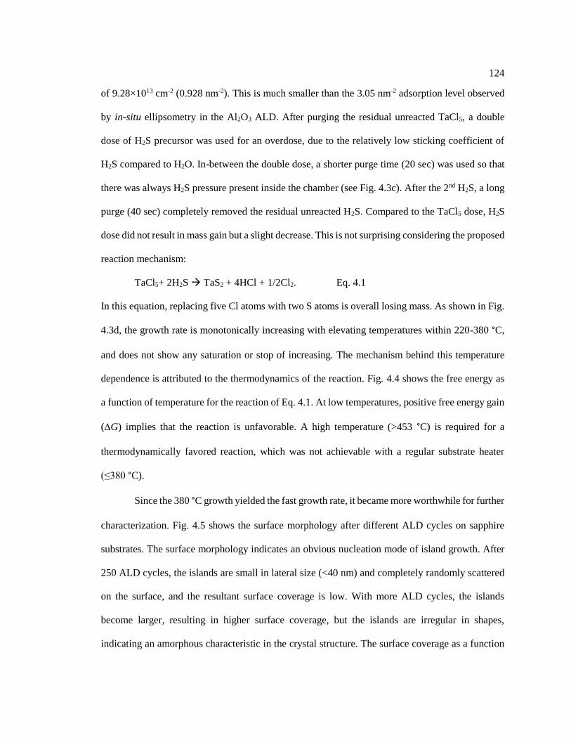
124
of 9.28×1013 cm-2 (0.928 nm-2). This is much smaller than the 3.05 nm-2 adsorption level observed
by in-situ ellipsometry in the Al2O3 ALD. After purging the residual unreacted TaCl5, a double
dose of H2S precursor was used for an overdose, due to the relatively low sticking coefficient of
H2S compared to H2O. In-between the double dose, a shorter purge time (20 sec) was used so that
there was always H2S pressure present inside the chamber (see Fig. 4.3c). After the 2nd H2S, a long
purge (40 sec) completely removed the residual unreacted H2S. Compared to the TaCl5 dose, H2S
dose did not result in mass gain but a slight decrease. This is not surprising considering the proposed
reaction mechanism:
TaCl5+ 2H2S TaS2 + 4HCl + 1/2Cl2. Eq. 4.1
In this equation, replacing five Cl atoms with two S atoms is overall losing mass. As shown in Fig.
4.3d, the growth rate is monotonically increasing with elevating temperatures within 220-380 °C,
and does not show any saturation or stop of increasing. The mechanism behind this temperature
dependence is attributed to the thermodynamics of the reaction. Fig. 4.4 shows the free energy as
a function of temperature for the reaction of Eq. 4.1. At low temperatures, positive free energy gain
(G) implies that the reaction is unfavorable. A high temperature (>453 °C) is required for a
thermodynamically favored reaction, which was not achievable with a regular substrate heater
(≤380 °C).
Since the 380 °C growth yielded the fast growth rate, it became more worthwhile for further
characterization. Fig. 4.5 shows the surface morphology after different ALD cycles on sapphire
substrates. The surface morphology indicates an obvious nucleation mode of island growth. After
250 ALD cycles, the islands are small in lateral size (<40 nm) and completely randomly scattered
on the surface, and the resultant surface coverage is low. With more ALD cycles, the islands
become larger, resulting in higher surface coverage, but the islands are irregular in shapes,
indicating an amorphous characteristic in the crystal structure. The surface coverage as a function
125
of the ALD cycles is shown in Fig. 4.5b. Even with 1000 ALD cycles (took ~27 hrs, not including
the heating and cooling time), the surface coverage is only ~61 %. Another interesting observation
is that with increasing ALD cycle number, the island height stays relatively unchanged at ~2 nm,
corresponding to ~3 monolayers of 1T-TaS2 (see the AFM line scans in Fig. 4.5a). The preference
of lateral nucleation and island growth mode has been commonly observed in the CVD growths of
TMD materials, as mentioned above. [62,171,172] This effect can be understood as a result of
strong in-plane anisotropy of TMD materials. In the out-of-plane direction, the atoms are fully
coordinated with no dangling bond available for nucleation, while the dangling bonds on the edge
of the material allows for further lateral growth. A further examination by a room temperature
Raman spectroscopy confirmed a relatively weak vibrational mode at 71.1 cm-1, which is close to
the previous report for the primary peak of 1T-TaS2 at 310 K (peaking at ~70 cm-1). Unfortunately,
due to the limitation of facility, we were unable to verify the low temperature characteristics of
Raman spectrum.
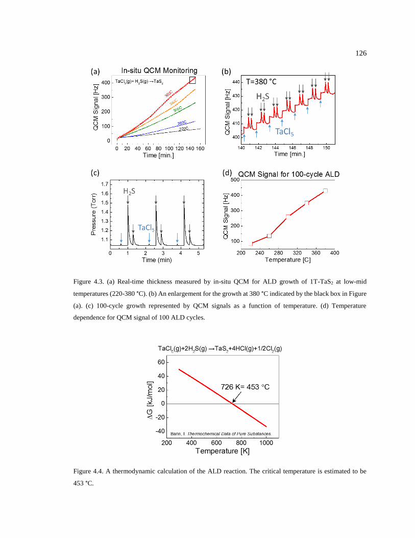
126
Figure 4.3. (a) Real-time thickness measured by in-situ QCM for ALD growth of 1T-TaS2 at low-mid
temperatures (220-380 °C). (b) An enlargement for the growth at 380 °C indicated by the black box in Figure
(a). (c) 100-cycle growth represented by QCM signals as a function of temperature. (d) Temperature
dependence for QCM signal of 100 ALD cycles.
Figure 4.4. A thermodynamic calculation of the ALD reaction. The critical temperature is estimated to be
453 °C.
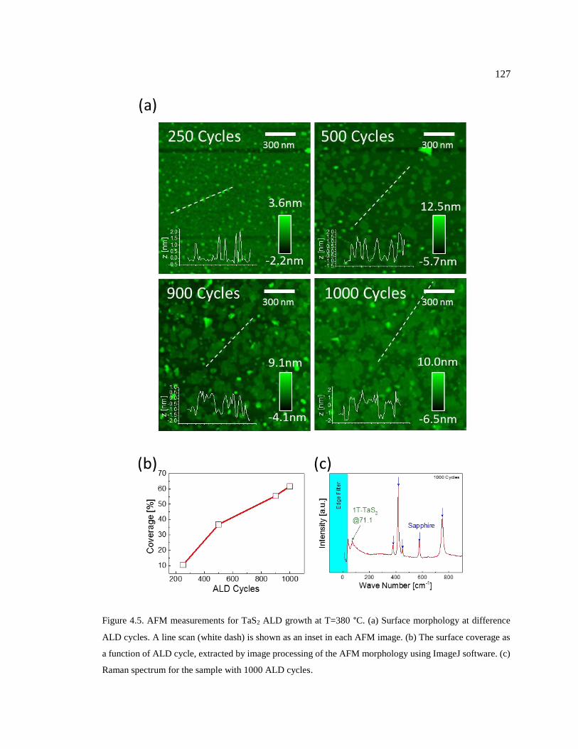
127
Figure 4.5. AFM measurements for TaS2 ALD growth at T=380 °C. (a) Surface morphology at difference
ALD cycles. A line scan (white dash) is shown as an inset in each AFM image. (b) The surface coverage as
a function of ALD cycle, extracted by image processing of the AFM morphology using ImageJ software. (c)
Raman spectrum for the sample with 1000 ALD cycles.

128
4.2.3 ALD growth at high temperatures
From the low-mid temperature results, the direct ALD growth of 1T-TaS2 requires a high
temperature (>453 °C) to obtain the desired material qualities. For this purpose, the substrate heater
of the ALD system has been upgraded, using a new design as shown in Section 2.1.3. The new
heater allows for a high temperature up to 480 °C with a power input of ~70 %. An even higher
temperature application requires more power input and would significantly shorten the lifetime of
the heater (actually four heaters had been burned out before realizing this issue). Note that at high
temperatures, QCM basically loses its functionality due to: (i) the maximum temperature allowed
for the internal QCM heater is limited to (<400 °C), so the QCM signal cannot represent the reaction
process occurring on the sample surface due to the large temperature difference in-between; (ii)
even if upgrading the heater of QCM for the high temperature application, the Q-factor of QCM
starts significantly decreasing at elevated temperatures (>309 °C), [92] so one can expect that the
QCM signal will become extremely noisy and therefore unreliable at a high temperature like 480
°C.
Fig. 4.6 shows the surface morphology after 500 cycles of ALD growth using TaCl5+ H2S
at T=480 °C. Scattered bar-like islands can be found, with a lateral size of ~40 nm × 170 nm. The
line scan in the inset shows an island height of ~17.5 nm, while the ~33 nm height may be a double
stack. This quasi-1D characteristic cannot from an amorphous material, so indicates a different
crystalline structure. Previous reports showed that in Tantalum-Sulfur family, there is another
member, TaS3, which is also quasi-1D crystal structured material. [47,173,174] So the bar-shape
material grown by high temperature ALD is possibly TaS3. If this assumption stands true, it
indicates that the ALD growth is sulfur rich or in other words, Ta deficient. A Ta deficiency is not
surprising because regarding the high temperature of 480 °C used during the growth, a strong
129
thermal desorption of TaCl5 can be expected, which has been well identified generally in other
ALD growths. [31]
To address the possible desorption issue of TaCl5, before the TaCl5+ H2S ALD, an ultrathin
Ta2O5 seed layer was prepared by 10 ALD cycles using TaCl5 and H2O as the precursors at 480 °C.
Thereafter, 500 cycles of TaCl5+ H2S ALD were performed. The surface morphology of the as-
obtained sample is shown in Fig. 4.7. The first important characteristic is the observation of
hexagonal shapes in conjunction with a few triangles. The lateral size of these shapes varies from
~50 nm to ~300 nm, while the AFM line scans reveal multiple thicknesses, ranging from ~4.3 nm
to ~10.7 nm. Regarding to the aspect ratio between the lateral and vertical size, the as-grown
material is more like 2D. The overall surface coverage estimated by ImageJ processing gives ~74
%. Another characteristic is the observation of the string like feature, more prominent in the lower
half of the AFM image in Fig. 4.7. These string like features are different from the above-mentioned
quasi-1D shapes, and are more like nanowires.
Fig. 4.8 shows the Raman spectrum of the sample with 500 cycles of TaCl5+H2S ALD on
a Ta2O5/sapphire substrate. The 1T-TaS2-like peak around 70 cm-1 is still well identified, and shows
a much stronger intensity compared to the 380 °C ALD result, indicating an increase of the
crystallinity and/or the material volume ratio at the sample surface. Besides 1T-TaS2-like peak and
those sharp peaks indicated by blue arrows, there are another two unidentified characteristics in
Fig. 4.8, represented by open circle and rhombus, respectively. The two broad and low intensity
peaks indicated by rhombus locate around ~1300 and ~1600 cm-1, respectively. These wavenumber
shifts are close to the previous reports about Raman spectra for carbon nanotubes, 1352 and 1580
cm-1. [175] This correlation to carbon nanotubes may explain the strange nanowire like features
observation in AFM image of Fig. 4.7. The second unidentified characteristic is the high intensity
and broad peak (or maybe a few peaks) indicated by a circle around 300 cm-1. Since this
characteristic is so broad, it is difficult to find the peak position. To address this issue, a post
130
deposition anneal in a H2S/Ar atmosphere was performed in order to improve the crystallinity of
all the possible materials in the sample, and therefore yield shaper Raman peaks. The annealing
was performed using a quartz tube furnace. Before elevating the temperature, the furnace chamber
was pump and then flush with Ar gas for three times, so as to remove the residual air inside the
chamber. Then a mixed H2S/Ar flow was established to sustain a 1 atm. pressure (H2S partial
pressure ~100 mTorr) and the chamber was heated up. The steady stay at 900 °C was 20 min, and
thereafter the sample was cooled down inside the chamber with only flowing Ar. Before the
annealing, the ALD grown film on the substrate appeared black. But the high temperature anneal
seems removed most of the material on the substrate, leaving a sapphire like sample afterwards.
This was confirmed by the Raman measurement after anneal (Fig. 4.9b). The characteristic Raman
peak for 1T-TaS2 is significantly weakened, and the carbon nanotube peaks are almost gone. The
unidentified peak around 300 cm-1 now becomes easier to distinguish, which splits into three peaks
at 225, 289, and 337 cm-1, respectively. By comparing these peaks with a previous report, their
structure looks similar to that of TaS3. [176] So from this observation, we can say that the broad
“circle” peak may originate from TaS3, meaning a coexistence of 1T-TaS2 and TaS3.
In summary, 1T-TaS2 thin films has been synthesized using ALD approach. However, the
existence of impurity phase TaS3 and the issue of relatively small crystal sizes still need to be
addressed by further optimizing the ALD process.

131
Figure 4.6. AFM image after 500 cycles of TaCl5+ H2S ALD growth on a c-sapphire substrate.
Figure 4.7. AFM image after 500 cycles of TaCl5+ H2S ALD growth on a Ta2O5/c-sapphire substrate.
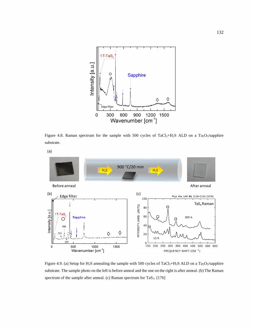
132
Figure 4.8. Raman spectrum for the sample with 500 cycles of TaCl5+H2S ALD on a Ta2O5/sapphire
substrate.
Figure 4.9. (a) Setup for H2S annealing the sample with 500 cycles of TaCl5+H2S ALD on a Ta2O5/sapphire
substrate. The sample photo on the left is before anneal and the one on the right is after anneal. (b) The Raman
spectrum of the sample after anneal. (c) Raman spectrum for TaS3. [176]
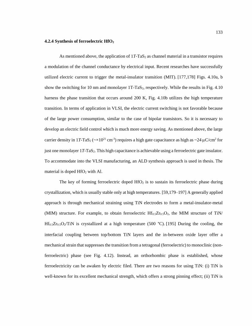
133
4.2.4 Synthesis of ferroelectric HfO2
As mentioned above, the application of 1T-TaS2 as channel material in a transistor requires
a modulation of the channel conductance by electrical input. Recent researches have successfully
utilized electric current to trigger the metal-insulator transition (MIT). [177,178] Figs. 4.10a, b
show the switching for 10 nm and monolayer 1T-TaS2, respectively. While the results in Fig. 4.10
harness the phase transition that occurs around 200 K, Fig. 4.10b utilizes the high temperature
transition. In terms of application in VLSI, the electric current switching is not favorable because
of the large power consumption, similar to the case of bipolar transistors. So it is necessary to
develop an electric field control which is much more energy saving. As mentioned above, the large
carrier density in 1T-TaS2 (~×1021 cm-3) requires a high gate capacitance as high as ~24 C/cm2 for
just one monolayer 1T-TaS2. This high capacitance is achievable using a ferroelectric gate insulator.
To accommodate into the VLSI manufacturing, an ALD synthesis approach is used in thesis. The
material is doped HfO2 with Al.
The key of forming ferroelectric doped HfO2 is to sustain its ferroelectric phase during
crystallization, which is usually stable only at high temperatures. [59,179–197] A generally applied
approach is through mechanical straining using TiN electrodes to form a metal-insulator-metal
(MIM) structure. For example, to obtain ferroelectric Hf0.5Zr0.5O2, the MIM structure of TiN/
Hf0.5Zr0.5O2/TiN is crystallized at a high temperature (500 °C). [195] During the cooling, the
interfacial coupling between top/bottom TiN layers and the in-between oxide layer offer a
mechanical strain that suppresses the transition from a tetragonal (ferroelectric) to monoclinic (non-
ferroelectric) phase (see Fig. 4.12). Instead, an orthorhombic phase is established, whose
ferroelectricity can be awaken by electric filed. There are two reasons for using TiN: (i) TiN is
well-known for its excellent mechanical strength, which offers a strong pinning effect; (ii) TiN is

134
conducting, can be used as electrodes and does not contribute to the capacitance/polarization of the
MIM structure.
The process flow of developing ferroelectric Al-doped HfO2 is shown in Fig. 4.12. A
heavily doped p-type Si was used as the substrate, because its high conductivity (~103 S/cm)
enables it to be the bottom electrode. The substrate was firstly degreased with acetone/IPA by
sonication. A hydrofluoric acid (HF 5%) treatment removed the surface native oxide, followed by
a DI-H2O rinse. Right after the wet-chemical clean, the Si substrates were transferred into the load
lock of a magnetron sputtering chamber, which was thereafter pumped down to ~10-6 Torr.
A 10 nm titanium nitride (TiN) thin film was deposited by a reactive sputtering using a
N2(30%) /Ar mixed gas at a 5 mTorr process pressure. The TiN growth rate was determined to be
1.12 nm/min, by AFM measurement of thickness step created using a shadow mask (Fig. 4.14a).
The TiN sputtering slight roughens the surface from ~0.1 nm to 0.563 nm (Fig. 4.14b). With the
thickness measured by AFM, a spectroscopic ellipsometry (SE) measurement allows to extract the
dielectric function of the sputtered TiN, which is close to that of bulk TiN (Fig. 4.14c). The
stoichiometric ratio of Ti: N was determined to be ~0.94 (Fig. 4.14d); regarding a typical ~5 %
error of XPS measurement in chemical composition, TiN films grown by sputtering is nearly
stoichiometric.
10 nm Al doped HfO2 films were deposited by ALD at 300 C. The stoichiometry of Al: Hf
ratio was controlled by varying the ALD cycles number of Al2O3 and HfO2. The thickness was in-
situ monitored by SE and fixed to be ~10 nm for all samples (Fig. 4.15). The growth parameters of
Al2O3 and HfO2 were the same as Table 2.1 in Section 2.1.2. Due to a higher temperature (300 °C)
for synthesizing ferroelectric HfO2, the growth rates (GPCs) were also slightly different (see Table
4.2). The stoichiometric ratio of Al: Hf was controlled by varying the cycle number ratio of Al2O3:
HfO2. The Al atomic percentage (Al atm %) can be calculated as follows:
135
2 3
2 3 2
Al O cycle # 1.406 Al atm %=
Al O cycle # 1.406 HfO cycle #
. Eq. 4.2
Samples with three different stoichiometric ratios were prepared in this thesis with purge HfO2, Al:
Hf=1:20 cycles (~6.6 atm% Al), and Al: Hf=1:10 cycles (~12.3 atm% Al).
After the ALD growth, the top TiN layer was deposited by the reactive sputtering, and then
the samples were annealed in a rapid thermal anneal (RTA) chamber at 900 °C/30 sec with a
ramping rate of 20 °C/sec and quenching rate of 240 °C/sec. At the later stage of cooling (<200 °C),
the temperature was able to follow the set point of cooling prole, and therefore cooled down
naturally.
Fig. 4.16 shows the process for defining the top electrode pattern. A Ti(5 nm)/Pt(50 nm)
layer was deposited by e-beam evaporation, with the pattern defined by a shadow mask. The
electrode size of the pattern was Ø=100 m circular shape. The pattern of top TiN layer was
developed using a SC1 solution (NH4OH:H2O2:H2O=1:2:7, 60 °C). The SC1 development of TiN
was optimized using an ex-situ ellipsometry (Fig. 4.17). The optimum time was determined to be
~2 min.
The electrical performance of the MIM structures were tested using a polarization vs
electric field measurement, or PE hysteresis loop with a frequency of 10 kHz. The MIM structure
using pure HfO2 as the insulator shows a significant characteristic of leakage current (Fig. 4.18a).
This can be attributed to the formation of grain boundary by the high temperature annealing, since
the grain boundary has a higher conductance. A 6.6% Al doping results in a hysteresis loop with a
remnant polarization Pr=1.8 C/cm2 and a coercivity EC=0.86 MV/cm. At high electric field, the
sample still shows a signature of leakage, which results in a drop in the polarization. A higher Al
doping of 12.3 % can further reduce the leakage current, but the PE hysteresis characteristic
disappears, while the small hysteresis may be caused by space charge trapped in the dielectric. The
dielectric constants of all three MIM structures are shown in Fig. 4.18d. The undoped sample shows
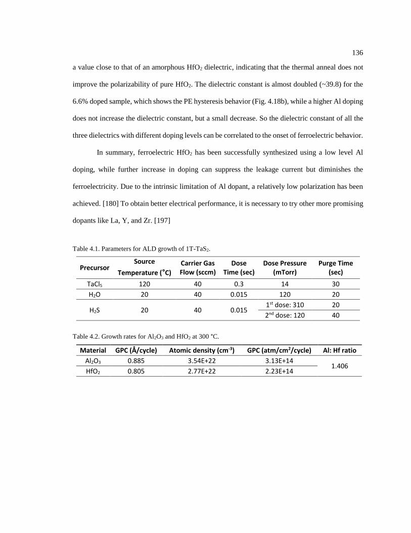
136
a value close to that of an amorphous HfO2 dielectric, indicating that the thermal anneal does not
improve the polarizability of pure HfO2. The dielectric constant is almost doubled (~39.8) for the
6.6% doped sample, which shows the PE hysteresis behavior (Fig. 4.18b), while a higher Al doping
does not increase the dielectric constant, but a small decrease. So the dielectric constant of all the
three dielectrics with different doping levels can be correlated to the onset of ferroelectric behavior.
In summary, ferroelectric HfO2 has been successfully synthesized using a low level Al
doping, while further increase in doping can suppress the leakage current but diminishes the
ferroelectricity. Due to the intrinsic limitation of Al dopant, a relatively low polarization has been
achieved. [180] To obtain better electrical performance, it is necessary to try other more promising
dopants like La, Y, and Zr. [197]
Table 4.1. Parameters for ALD growth of 1T-TaS2.
Precursor Source
Temperature (°C)
Carrier Gas Flow (sccm)
Dose Time (sec)
Dose Pressure (mTorr)
Purge Time (sec)
TaCl5 120 40 0.3 14 30
H2O 20 40 0.015 120 20
H2S 20 40 0.015 1st dose: 310 20
2nd dose: 120 40
Table 4.2. Growth rates for Al2O3 and HfO2 at 300 °C.
Material GPC (Å/cycle) Atomic density (cm-3) GPC (atm/cm2/cycle) Al: Hf ratio
Al2O3 0.885 3.54E+22 3.13E+14 1.406
HfO2 0.805 2.77E+22 2.23E+14
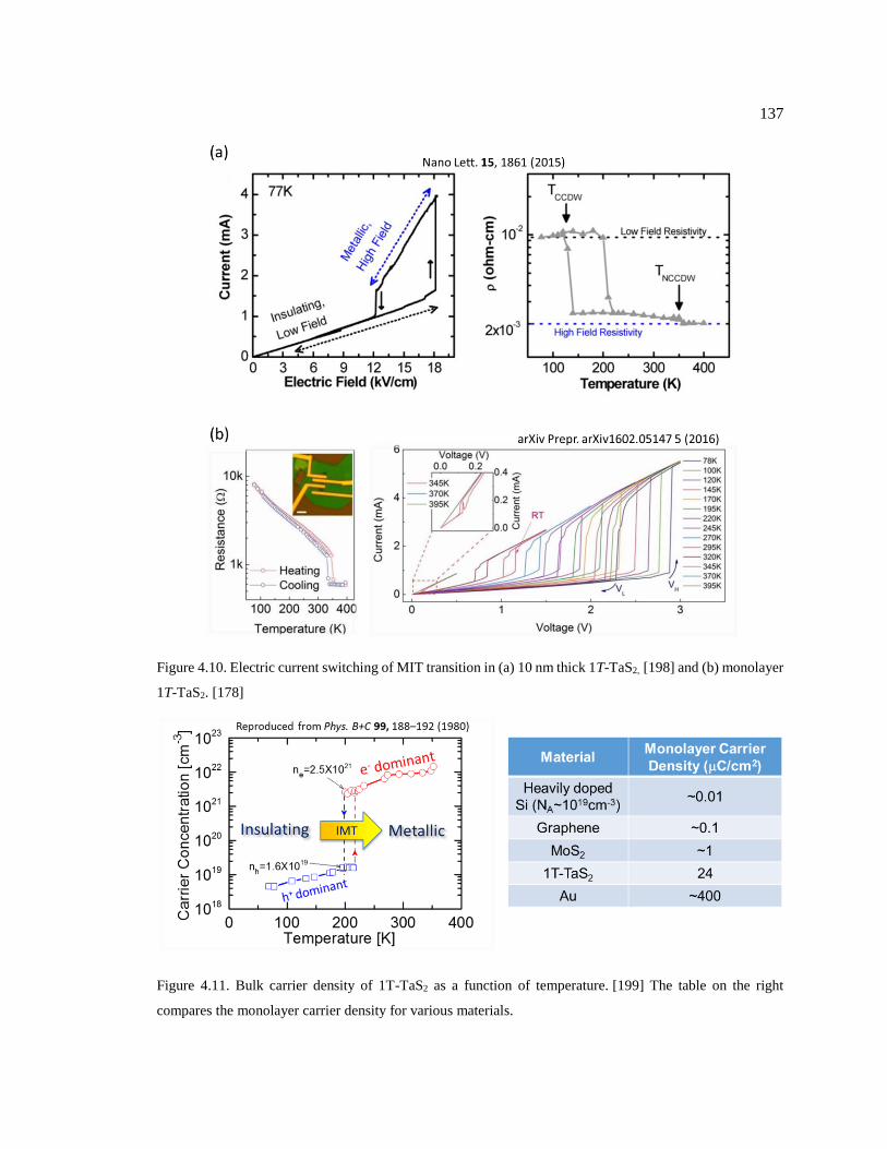
137
Figure 4.10. Electric current switching of MIT transition in (a) 10 nm thick 1T-TaS2, [198] and (b) monolayer
1T-TaS2. [178]
Figure 4.11. Bulk carrier density of 1T-TaS2 as a function of temperature. [199] The table on the right
compares the monolayer carrier density for various materials.

138
Figure 4.12. The mechanism of forming ferroelectric HfO2 at room temperature.
Figure 4.13. The process flow for developing Al doped HfO2 ferroelectrics.
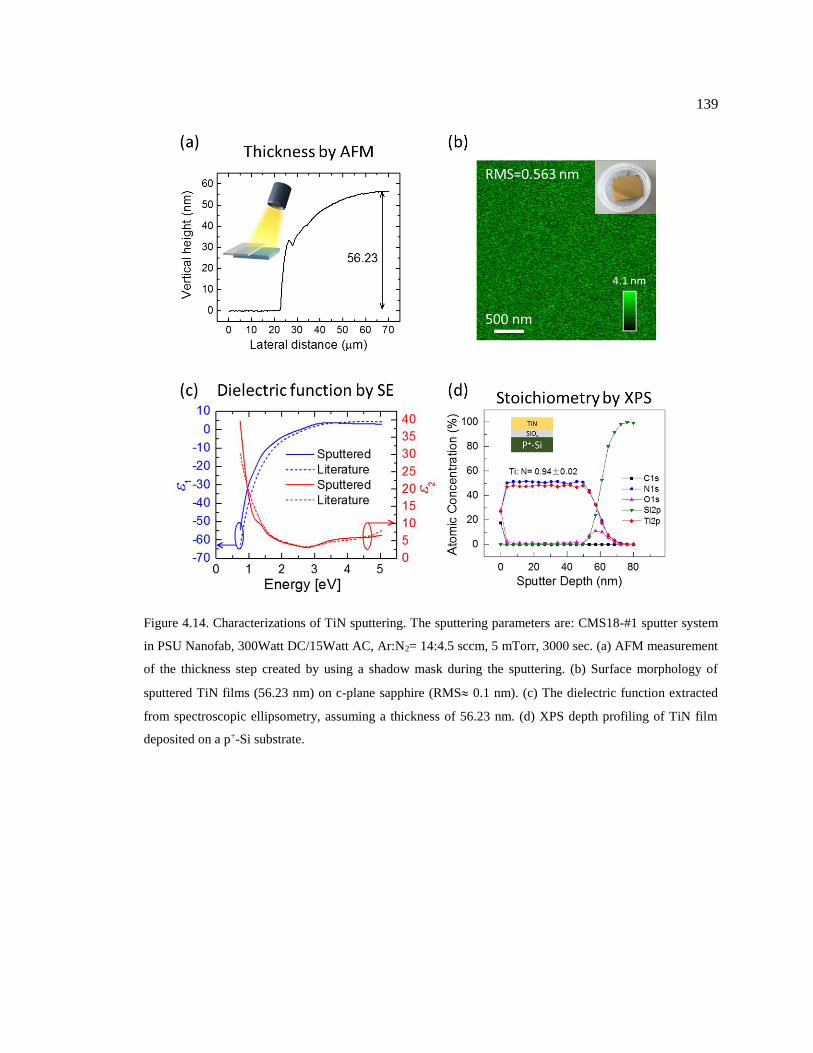
139
Figure 4.14. Characterizations of TiN sputtering. The sputtering parameters are: CMS18-#1 sputter system
in PSU Nanofab, 300Watt DC/15Watt AC, Ar:N2= 14:4.5 sccm, 5 mTorr, 3000 sec. (a) AFM measurement
of the thickness step created by using a shadow mask during the sputtering. (b) Surface morphology of
sputtered TiN films (56.23 nm) on c-plane sapphire (RMS 0.1 nm). (c) The dielectric function extracted
from spectroscopic ellipsometry, assuming a thickness of 56.23 nm. (d) XPS depth profiling of TiN film
deposited on a p+-Si substrate.

140
Figure 4.15. In-situ SE monitoring of 300 °C ALD growth for (a) Al2O3 calibration, (b) HfO2 calibration, and
(c) Al doped HfO2 with 1:20 cycle ratio.
Figure 4.16. Process of defining electrode pattern for measuring MIM.
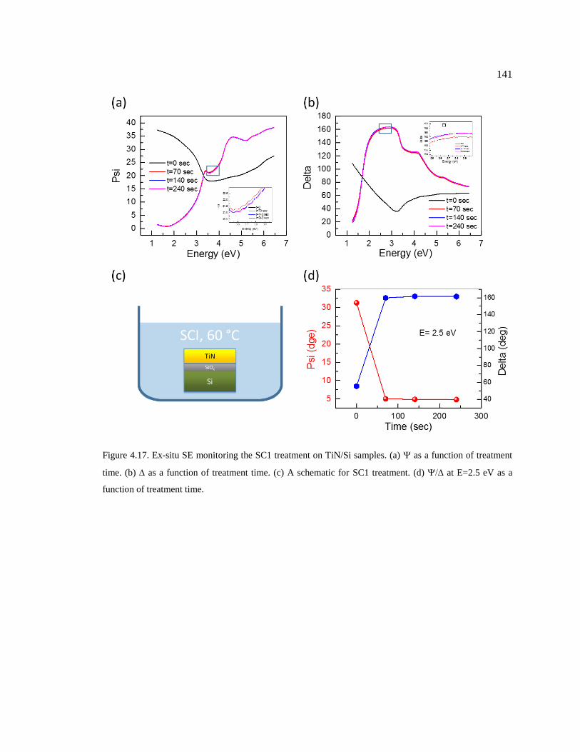
141
Figure 4.17. Ex-situ SE monitoring the SC1 treatment on TiN/Si samples. (a) as a function of treatment
time. (b) as a function of treatment time. (c) A schematic for SC1 treatment. (d) at E=2.5 eV as a
function of treatment time.
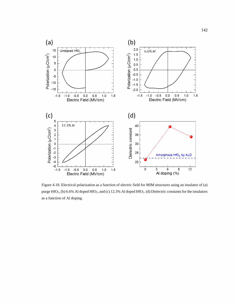
142
Figure 4.18. Electrical polarization as a function of electric field for MIM structures using an insulator of (a)
purge HfO2, (b) 6.6% Al doped HfO2, and (c) 12.3% Al doped HfO2. (d) Dielectric constants for the insulators
as a function of Al doping.
Chapter 5
Conclusions, Future Work and Outlook
In this thesis, the high-k deposition on Ge surface and synthesis of 1T-TaS2 thin films by
ALD approach have been addressed. For the first part, a combinatory method using wet-chemical
clean and in-situ H2 plasma has firstly been developed and optimized to obtain a pristine Ge surface.
Then starting from this clean surface, the surface chemistry dependence of the ALD nucleation has
been identified by combining in-situ probing, ex-situ metrologies and atomic scale simulations. The
understanding of the ALD mechanism enables the fabrication of a HfO2/Al2O3/GeOx trilayer gate
stack for Ge MOSCap devices, whose optimization has resulted in superior electrical performances.
For the second part, the temperature dependence of the growth kinetics has been discovered for 1T-
TaS2 ALD, and the resultant materials structures have been characterized. Also, a fabrication
process of ferroelectric HfO2 has been developed as a necessary element to be integrated in the
future field effect transistor fabrication. In particular, the following implications are highlighted:
Chapter 3 By comparing the results of the optimized Ge results discussed in this
thesis or published elsewhere, the electrical performance of Ge devices particularly their reliability
is still not lining up with that of Si. A deep thinking about this issue is necessary. For many related
phenomena, the origin is mostly pointing to the thermodynamics of the materials. A good example
is the significant difference in the interface quality between SiO2/Si and GeO2/Si. Unlike GeO2/Ge
interface which starts degrading at T>450 °C, the generation of SiO at SiO2/Si is extremely difficult
and requires a high activation temperature >1700 °C. [200] In this sense, at a process temperature
of 270 °C, the SiO2/Si interface is ~exp[(1700-450)/543]10 times more than GeO2/Ge. To
overcome this fundamental difference in thermodynamics, there can be two routes. One is to use
144
“external support” like introducing N, Al atoms into GeO2 and forming an intermixing network,
like Ge-O-Al or O-Ge-N (or Ge-O-N), which chemically strengthens the material stability. This
approach potentially inhibits the formation of gas phase GeO, but does not necessarily suppress the
Ge-O bond breaking in the dielectric and at the interface. This probably explains that rather than
healing the in-gap trap states in the semiconductor side, the intermixing [Al2O3/GeOx] interlayer is
more effective to address the border trap states in the dielectric. Another possible solution is to
directly use an oxygen free surface passivation like Ge3N4, which has resulted in even better
interface qualities. [11] However, the relatively low band gap (≤4.0 eV) [201,202] and low
dielectric constant (k≤ 6.27) [202] of Ge3N4 have limited its application as a gate insulator. Thus, a
thickness downscaling without compromising the interface quality is necessary, which still remains
an unclarified issue. In summary, in the future research of Ge transistors, the interface stabilization
will continue as one of major topics.
Another implication is about the ALD nucleation of dielectrics. As confirmed in this thesis,
a direct ALD on a H-terminated Ge surface is highly localized growth and yields a non-conformal
and defective dielectric, as indicated by the high leakage current and high density of border trap
states. Similar effect has been also confirmed on Ge using other thermodynamically stable
dielectrics like ZrO2, [18] as well as in Al2O3/Si MOSCaps. [203] In the case of Si, the interface
and dielectric properties can be effectively healed by a high temperature anneal, which however is
not favorable for Ge. One of the major successes of employing an ultrathin GeOx layer as the
surface passivation is boosting the initial nucleation of the subsequent ALD, allowing for a
boundary/pinhole free dielectric. In this sense, when developing Ge devices with new structures
made of new materials, the nonlinear initial nucleation behavior and the resultant material
properties should always be considered as the investigation of first priority, rather than simply using
a process matrix that only controls the ALD cycles or the so-called “thickness”.
145
Chapter 4 The synthesis of 1T-TaS2 generally requires a high thermal energy to
obtain high quality materials. This trend has been well reflected in the temperature dependence of
ALD growth, while low temperature growth only yielded nearly amorphous material, much better
defined crystals were observed after a high temperature ALD. The high temperature requirement
can be even better clarified by comparing the ALD results with the other high temperature results
produced by a CVD approach using very similar reaction precursors. [74] The CVD growth yielded
large crystal size (~10 m) with high crystallinity, and more importantly, well behaved electrical
characteristics. However, just like most of CVD growth of other 2D materials, the low surface
coverage remains as a challenging issue, limiting the potential batch fabrication of integrating 1T-
TaS2 in VLSI technology. So far, there are very few reports about synthesizing wafer-scale,
coalesced, and ultrathin 2D material films, [64] Thus, the synthesizing wafer-scale and high-quality
1T-TaS2 is still a non-trivial research topic in the future.
In going forward, there are a few ideas or research projects that can be imagined, as follows:
Further optimization of [Al2O3/GeOx]/Ge interface. Early trial experiments using an O2
plasma enhanced HfO2 ALD directly on a clean Ge surface has yielded a low Dit interface right
after the device fabrication, but the properties degraded quickly due to the unstable HfO2/GeO2/Ge
structure in the devices. So from this point of view, instead of growing stabilization oxide on a
GeOx/Ge surface, a direct O2 plasma enhanced Al2O3 or ZrO2 ALD on Ge is expected to create a
superior and stable dielectric/Ge interface. The ZrO2 PEALD would be more straightforward,
because the gate dielectric growth could be finished in one deposition process; also it might yield
better performance in terms of EOT scaling, due to its high dielectric constant (k~24).
Integrating ultrathin Ge3N4 as the surface passivation on Ge. Ge3N4 could be used as
the interlayer between the high-k dielectric and Ge substrate for further improvement of electrical
performance. The Ge3N4 could potentially be prepared by the in-situ plasma source using N2 as the
reactive gas. Process optimization and material characterization of Ge3N4 would be necessary. The
146
subsequent ALD nucleation mechanism should be carefully addressed using the in-situ
spectroscopic ellipsometry, which would entail the thickness evaluation and modeling of the
material optical constants. The goal is to obtain a highly scaled (EOT ≤0.5 nm) and electrically
reliable Ge devices (MOSCaps, MOSFETs, or even FinFETs).
Mechanism study of ALD growth of 1T-TaS2. The results presented in this thesis has
shown that the nucleation of 1T-TaS2 can be assisted by using a Ta2O5 seed layer. The detailed
mechanism remains not crystal-clear yet. A possible experiment that can be done to figure out the
mechanism is to use a patterned Ta2O5 layer on sapphire substrates with various sizes, separations,
geometries, and thickness as the starting surface in the TaCl5 +H2S ALD.
Improving electrical performance of ferroelectric HfO2. While the Al doping HfO2 is
intrinsically limited in the polarization performance, other dopants like La, Zr, and Y have been
reported to induce much larger polarization (>20 C/cm2). [197] An even more interesting idea is
to utilize the antiferroelectric gate insulator, which does not show the unwanted large hysteresis at
low electric fields, but still sustains a sufficiently high capacitance density at high electric
fields. [195]
Fabricating ferroelectric field effect transistors (FeFETs) using 1T-TaS2 channel.
With the 1T-TaS2 growth and high capacitance gate insulator addressed above, the FeFETs
fabrication of 1T-TaS2 becomes possible. A plausible device structure is using a back-gated thin
film transistor (TFT) design. While a direct ALD growth of gate insulator on TMD materials has
been proven difficult, the TFT structure allows for the following process: (i) firstly MIM synthesis
of ferroelectric HfO2 first, (ii) removal of top TiN to expose the gate insulator, (iii) growth of 1T-
TaS2 thin film on top of gate insulator, and (iv) growth of the protection capping layer (can be
anything without concerning EOT scaling and therefore can be very thick).
After looking backward the VLSI history, the Moore’s law has been surviving for more
than 50 years and resulted state-of-art technologies. Whenever, the technology encountered

147
bottlenecks, researchers in academia and industries always came up with genius ideas to
successfully tackle the issue. With the 5 nm node commercialized today, moving further towards 3
nm and even 2 nm technology is challenging but inevitable. Among all the possible future routes
of the technology development, integrating novel channel materials appears the most promising.
Maybe it is too arbitrary to say: “long live Moore’s law”, but the industry people generally believe
the law is not dead yet.
Reference
[1] Y. Taur and T. H. Ning, Fundamentals of Modern VLSI Devices, 2nd ed. (2009).
[2] Https://en.wikipedia.org/wiki/Bipolar_junction_transistor
[3] Http://electroiq.com/blog/2015/11/what-lies-beneath-50-years-of-enabling-moores-law/
[4] Https://arstechnica.com/gadgets/2017/06/ibm-5nm-chip/
[5] S.-H. Lo, D. A. Buchanan, Y. Taur, and W. Wang, IEEE Electron Device Lett. 18, 209 (1997).
[6] Https://web.stanford.edu/class/ee410/AdvCMOS.pdf
[7] Https://archive.cnx.org/contents/6d846a17-ee19-4663-afb7-b49448117e99@1/sspd-chapter-2-1-3-
nano-technology-era
[8] Http://archive.eetasia.com/www.eetasia.com/ART_8800667494_499489_NT_02adb57c.HTM
[9] Https://web.stanford.edu/class/ee311/NOTES/TrendsSlides.pdf
[10] Y. Kamata, Mater. Today 11, 30 (2008).
[11] S. Takagi, T. Maeda, N. Taoka, M. Nishizawa, Y. Morita, K. Ikeda, Y. Yamashita, M. Nishikawa,
H. Kumagai, R. Nakane, S. Sugahara, and N. Sugiyama, Microelectron. Eng. 84, 2314 (2007).
[12] S. K. Wang, K. Kita, C. H. Lee, T. Tabata, T. Nishimura, K. Nagashio, and A. Toriumi, J. Appl.
Phys. 108, 54104 (2010).
[13] K. Prabhakaran, F. Maeda, Y. Watanabe, and T. Ogino, Appl. Phys. Lett. 76, 2244 (2000).
[14] Y. Kamata, Y. Kamimuta, T. Ino, and A. Nishiyama, Jpn. J. Appl. Phys. 44, 2323 (2005).
[15] A. Toriumi, T. Tabata, C. Hyun Lee, T. Nishimura, K. Kita, and K. Nagashio, Microelectron. Eng.
86, 1571 (2009).
[16] S. N. a Murad, P. T. Baine, D. W. McNeill, S. J. N. Mitchell, B. M. Armstrong, M. Modreanu, G.
Hughes, and R. K. Chellappan, Solid. State. Electron. 78, 136 (2012).
[17] S. Abermann, O. Bethge, C. Henkel, and E. Bertagnolli, Appl. Phys. Lett. 94, 262904 (2009).
[18] C. O. Chui, S. Ramanathan, B. B. Triplett, P. C. McIntyre, and K. C. Saraswat, IEEE Electron Device
Lett. 23, 473 (2002).
149
[19] V. V. Afanas’ev, Y. G. Fedorenko, and A. Stesmans, Appl. Phys. Lett. 87, 32107 (2005).
[20] K. Devloo-Casier, J. Dendooven, K. F. Ludwig, G. Lekens, J. D’Haen, and C. Detavernier, Appl.
Phys. Lett. 98, 231905 (2011).
[21] Y. Oshima, Y. Sun, D. Kuzum, T. Sugawara, K. C. Saraswat, P. Pianetta, and P. C. McIntyre, J.
Electrochem. Soc. 155, G304 (2008).
[22] E. P. Gusev, H. Shang, M. Copel, M. Gribelyuk, C. D’Emic, P. Kozlowski, and T. Zabel, Appl. Phys.
Lett. 85, 2334 (2004).
[23] F. Gao, S. J. Lee, J. S. Pan, L. J. Tang, and D. L. Kwong, Appl. Phys. Lett. 86, 1 (2005).
[24] R. Zhang, T. Iwasaki, N. Taoka, M. Takenaka, and S. Takagi, J. Electrochem. Soc. 158, G178 (2011).
[25] F. G. N. W. C. X. Z. J. S. P. L. J. T. D. L. K. S. J. Whang S. J. Lee, Iedm2004 12.6.1 (2004).
[26] R. Zhang, T. Iwasaki, N. Taoka, M. Takenaka, and S. Takagi, in VLSI Technol. (VLSIT), 2011 Symp.
(IEEE, 2011), pp. 56–57.
[27] R. Zhang, P. Huang, N. Taoka, M. Takenaka, and S. Takagi, Symp. VLSI Technol. 161 (2012).
[28] T. Maeda, M. Nishizawa, Y. Morita, and S. Takagi, Appl. Phys. Lett. 90, 72911 (2007).
[29] R. Zhang, P. C. Huang, J. C. Lin, M. Takenaka, and S. Takagi, Tech. Dig. - Int. Electron Devices
Meet. IEDM 1, 371 (2012).
[30] O. Sneh, R. B. Clark-Phelps, A. R. Londergan, J. Winkler, and T. E. Seidel, Thin Solid Films 402,
248 (2002).
[31] S. M. George, Chem. Rev. 110, 111 (2010).
[32] Http://www.ioffe.ru/SVA/NSM/Semicond/, (n.d.).
[33] I. Barin, Thermochemical Data of Pure Substances, Thermochemical Data of Pure Substances
(Wiley-VCH, 1997).
[34] C. Kittel, Introduction to Solid State Physics (Wiley, 2005).
[35] Y. Zheng, S. Hong, G. Psofogiannakis, G. B. Rayner Jr, S. Datta, A. C. T. van Duin, R. Engel-
Herbert, G. B. Rayner, S. Datta, A. C. T. Van Duin, and R. Engel-Herbert, ACS Appl. Mater.
Interfaces 9, 15848 (2017).
[36] K. S. Novoselov, D. Jiang, F. Schedin, T. J. Booth, V. V Khotkevich, S. V Morozov, and A. K. Geim,
150
Proc. Natl. Acad. Sci. U. S. A. 102, 10451 (2005).
[37] K. S. Novoselov, A. K. Geim, S. V Morozov, D. Jiang, Y. Zhang, S. V Dubonos, I. V Grigorieva,
and A. A. Firsov, Science (80-. ). 306, 666 (2004).
[38] A. Winchester, S. Ghosh, S. Feng, A. L. Elias, T. Mallouk, M. Terrones, and S. Talapatra, ACS Appl.
Mater. Interfaces 6, 2125 (2014).
[39] A. Catellani, M. Posternak, A. Baldereschi, H. J. F. Jansen, and A. J. Freeman, Phys. Rev. B 32, 6997
(1985).
[40] R. Kershaw, M. Vlasse, and A. Wold, Inorg. Chem. 6, 1599 (1967).
[41] F. J. Di Salvo and J. E. Graebner, Solid State Commun. 23, 825 (1977).
[42] B. Sipos, a F. Kusmartseva, A. Akrap, H. Berger, L. Forró, and E. Tutis, Nat. Mater. 7, 960 (2008).
[43] F. J. Di Salvo, J. a. Wilson, B. G. Bagley, and J. V. Waszczak, Phys. Rev. B 12, 2220 (1975).
[44] H. Mutka, L. Zuppiroli, P. Molinié, and J. C. Bourgoin, Phys. Rev. B 23, 5030 (1981).
[45] Y. Zhou and S. Ramanathan, Crit. Rev. Solid State Mater. Sci. 38, 286 (2013).
[46] P. Darancet, A. J. Millis, and C. a. Marianetti, Phys. Rev. B 90, 2 (2014).
[47] F. Jellinek, J. Less-Common Met. 4, 9 (1962).
[48] P. Schmidt, J. Kröger, B. M. Murphy, and R. Berndt, New J. Phys. 10, 13022 (2008).
[49] A. Spijkerman, J. L. de Boer, A. Meetsma, G. A. Wiegers, and S. van Smaalen, Phys. Rev. B 56,
13757 (1997).
[50] K. Rossnagel and N. V Smith, Phys. Rev. B 73, 73106 (2006).
[51] M. Capone, L. Capriotti, F. Becca, and S. Caprara, 63, 5 (2000).
[52] N. F. Mott, Philos. Mag. 6, 287 (1961).
[53] P. P. Edwards and M. J. Sienko, Acc. Chem. Res. 15, 87 (1982).
[54] Y. Yu, F. Yang, X. F. Lu, Y. J. Yan, Y. Cho, L. Ma, X. Niu, S. Kim, Y. Son, D. Feng, S. Li, S.
Cheong, X. H. Chen, and Y. Zhang, Nat. Nanotechnol. 10, 1 (2015).
[55] M. Imada, A. Fujimori, and Y. Tokura, Rev. Mod. Phys. 70, 1039 (1998).
[56] Y. W. Yin, J. D. Burton, Y.-M. Kim, A. Y. Borisevich, S. J. Pennycook, S. M. Yang, T. W. Noh, A.
Gruverman, X. G. Li, E. Y. Tsymbal, and Q. Li, Nat. Mater. 12, 1 (2013).
151
[57] H. Fujishiro, T. Fukase, and M. Ikebe, J. Phys. Soc. Japan 70, 628 (2001).
[58] Y. Liu, R. Ang, W. J. Lu, W. H. Song, L. J. Li, and Y. P. Sun, Appl. Phys. Lett. 102, 1 (2013).
[59] D. Martin, E. Yurchuk, S. Müller, J. Müller, J. Paul, J. Sundquist, S. Slesazeck, T. Schlösser, R. Van
Bentum, M. Trentzsch, U. Schröder, and T. Mikolajick, Solid. State. Electron. 88, 65 (2013).
[60] N. V Smith, S. D. Kevan, and F. J. DiSalvo, J. Phys. C Solid State Phys. 18, 3175 (1985).
[61] X. L. Wu and C. M. Lieber, Science (80-. ). 243, 1703 (1989).
[62] K. Xu, L. Yin, Y. Huang, T. A. Shifa, J. Chu, F. Wang, R. Cheng, Z. Wang, and J. He, Nanoscale 8,
16802 (2016).
[63] Y. Gong, Z. Liu, A. R. Lupini, G. Shi, J. Lin, S. Najmaei, Z. Lin, A. Laura, A. Berkdemir, G. You,
H. Terrones, M. Terrones, R. Vajtai, S. T. Pantelides, S. J. Pennycook, J. Lou, W. Zhou, and P. M.
Ajayan, Nano Lett. 14, 442 (2014).
[64] K. Kang, S. Xie, L. Huang, Y. Han, P. Y. Huang, K. F. Mak, C.-J. Kim, D. Muller, and J. Park,
Nature 520, 656 (2015).
[65] D. Liu, W. Zhang, D. Mou, J. He, Y.-B. Ou, Q.-Y. Wang, Z. Li, L. Wang, L. Zhao, S. He, Y. Peng,
X. Liu, C. Chen, L. Yu, G. Liu, X. Dong, J. Zhang, C. Chen, Z. Xu, J. Hu, X. Chen, X. Ma, Q. Xue,
and X. J. Zhou, Nat. Commun. 3, 931 (2012).
[66] J. Lauth, F. E. S. Gorris, M. Samadi Khoshkhoo, T. Chassé, W. Friedrich, V. Lebedeva, A. Meyer,
C. Klinke, A. Kornowski, M. Scheele, and H. Weller, Chem. Mater. 28, 1728 (2016).
[67] M. J. Hollander, Y. Liu, W.-J. Lu, J. Li, Y.-P. Sun, J. a. Robinson, and S. Datta, Nano Lett. 15, 1861
(2015).
[68] A. Luican-Mayer, J. R. Guest, and S.-W. Hla, arXiv Prepr. arXiv1506.04102 (2015).
[69] X. Yu, T. Jia, and L. Zou, arXiv 1407, 1407 (2014).
[70] M. Yoshida, Y. Zhang, J. Ye, R. Suzuki, Y. Imai, S. Kimura, A. Fujiwara, and Y. Iwasa, Sci. Rep. 4,
1 (2014).
[71] Y. Fujisawa, T. Shimabukuro, H. Kojima, K. Kobayashi, S. Demura, and H. Sakata, IOP Conf. Ser.
J. Phys. Conf. Ser. 871, 12003 (2017).
[72] S. Tanda, T. Sambongi, T. Tani, and S. Tanaka, J. Phys. Socitey Japan 53, 476 (1984).

152
[73] S. Dunning-Riley and S. Merryfield, Nursing (Lond). 44, 8 (2014).
[74] W. Fu, Y. Chen, J. Lin, X. Wang, Q. Zeng, J. Zhou, L. Zheng, H. Wang, Y. He, H. He, Q. Fu, K.
Suenaga, T. Yu, and Z. Liu, Chem. Mater. 28, 7613 (2016).
[75] P. Schmidt, M. Binnewies, R. Glaum, and M. Schmidt, in Adv. Top. Cryst. Growth (InTech, 2013).
[76] A. Ubaldini and E. Giannini, J. Cryst. Growth 401, 878 (2014).
[77] Y. Shi, W. Zhou, A.-Y. Lu, W. Fang, Y.-H. Lee, A. L. Hsu, S. M. Kim, K. K. Kim, H. Y. Yang, L.-
J. Li, J.-C. Idrobo, and J. Kong, Nano Lett. 12, 2784 (2012).
[78] L. K. Tan, B. Liu, J. H. Teng, S. Guo, H. Y. Low, and K. P. Loh, Nanoscale 6, 10584 (2014).
[79] E. Ahvenniemi, A. R. Akbashev, S. Ali, M. Bechelany, M. Berdova, S. Boyadjiev, D. C. Cameron,
R. Chen, M. Chubarov, V. Cremers, A. Devi, V. Drozd, L. Elnikova, G. Gottardi, K. Grigoras, D. M.
Hausmann, C. S. Hwang, S.-H. Jen, T. Kallio, J. Kanervo, I. Khmelnitskiy, D. H. Kim, L. Klibanov,
Y. Koshtyal, A. O. I. Krause, J. Kuhs, I. Kärkkänen, M.-L. Kääriäinen, T. Kääriäinen, L. Lamagna,
A. A. Łapicki, M. Leskelä, H. Lipsanen, J. Lyytinen, A. Malkov, A. Malygin, A. Mennad, C. Militzer,
J. Molarius, M. Norek, Ç. Özgit-Akgün, M. Panov, H. Pedersen, F. Piallat, G. Popov, R. L. Puurunen,
G. Rampelberg, R. H. A. Ras, E. Rauwel, F. Roozeboom, T. Sajavaara, H. Salami, H. Savin, N.
Schneider, T. E. Seidel, J. Sundqvist, D. B. Suyatin, T. Törndahl, J. R. van Ommen, C. Wiemer, O.
M. E. Ylivaara, and O. Yurkevich, J. Vac. Sci. Technol. A Vacuum, Surfaces, Film. 35, 10801 (2017).
[80] M. Leskelä and M. Ritala, Angew. Chemie Int. Ed. 42, 5548 (2003).
[81] International Technology Roadmap for Semiconductors, 2007 Edition (n.d.).
[82] a. C. Dillon, A. W. Ott, J. D. Way, and S. M. George, Surf. Sci. 322, 230 (1995).
[83] J. D. Ferguson, A. W. Weimer, and S. M. George, Thin Solid Films 371, 95 (2000).
[84] A. W. W. Ott, J. W. W. Klaus, J. M. M. Johnson, and S. M. M. George, Thin Solid Films 292, 135
(1997).
[85] Y. Widjaja and C. B. Musgrave, Appl. Phys. Lett. 80, 3304 (2002).
[86] Y. Xu and C. B. Musgrave, Chem. Mater. 16, 646 (2004).
[87] G. S. Higashi and C. G. Fleming, Appl. Phys. Lett. 55, 1963 (1989).
[88] B. Lux, C. Colombier, H. Altena, and K. Stjernberg, Thin Solid Films 138, 49 (1986).
153
[89] M. D. Groner, F. H. Fabreguette, J. W. Elam, and S. M. George, Chem. Mater. 16, 639 (2004).
[90] R. Puurunen, Chem. Vap. Depos. 9, 249 (2003).
[91] Z. Chen, H. Wang, X. Wang, P. Chen, Y. Liu, H. Zhao, Y. Zhao, Y. Duan, S. Y. Chen, C. F. Lai, R.
H. Hwang, Y. H. Lai, M. S. Wang, A. Forkan, I. Khalil, Z. Tari, J. Lee, Z. T. Zhang, L. Liu, Y. Yu,
C. Yan, K. Li, Z. Zheng, S. Reineke, T. H. Han, H. Aziz, Z. D. Popovic, N. X. Hu, A. M. Hor, G.
Xu, M. S. Xu, J. B. Xu, H. Z. Chen, M. Wang, A. B. Chwang, A. P. Ghosh, L. J. Gerenser, C. M.
Jarman, J. E. Fornalik, L. H. Kim, M. Li, D. W. Choi, F. Nehm, C. Y. Park, J. S. An, H. J. Jang, J.
H. Lee, B. H. Choi, Y. Y. Lin, Y. N. Chang, M. H. Tseng, C. C. Wang, F. Y. Tsai, W. M. Yun, Y.
Duan, P. Sundberg, A. Sood, X. Liu, M. Karppinen, B. Yoon, B. H. Lee, S. M. George, J. Meyer, H.
Schmidt, W. Kowalsky, T. Riedl, A. Kahn, Z. Giedraityte, P. Sundberg, M. Karppinen, D. S. Han,
D. K. Choi, J. W. Park, S. Feng-Bo, B. H. Lee, K. H. Lee, S. Im, M. M. Sung, P. Saint-Cast, H. C.
Knoops, P. Sundberg, M. Karppinen, B. Yoon, D. Seghete, A. S. Cavanagh, S. M. George, Y.
Tomczak, K. Knapas, M. Sundberg, M. Leskela, M. Ritala, R. L. Puurunen, V. Miikkulainen, M.
Leskela, M. Ritala, R. L. Puurunen, K. Ali, K. H. Choi, C. Hossbach, and S. Lee, Sci. Rep. 7, 40061
(2017).
[92] T. J. Larrabee, A Quantified Dosing ALD Reactor with in-Situ Diagnostics for Surface Chemistry
Studies, The Pennsylvania State University, 2012.
[93] D. R. Sadoway and S. N. Flengas, Can. J. Chem. 54, 1692 (1976).
[94] J. N. Hilfiker and R. A. Synowicki, Solid State Technol. 39, 157 (1996).
[95] E. A. I. (Editors) R.W.Collins, D.E.Aspnes, Solid Thin Film. 313–314, 1 (1998).
[96] H. G. Tompkins and E. A. Irene, Handbook of Ellipsometry (William Andrew, 2005).
[97] H. Fujiwara, Spectroscopic Ellipsometry: Principles and Applications (John Wiley & Sons, 2007).
[98] G. N. Maracas, J. L. Edwards, K. Shiralagi, K. Y. Choi, R. Droopad, B. Johs, and J. A. Woolam, J.
Vac. Sci. Technol. A 10, 1832 (1992).
[99] G. E. J. Jr and F. A. Modine, Appl. Phys. Lett 69, 371 (1996).
[100] G. Bemski, Proc. IRE 46, 990 (1958).
[101] M. Houssa, G. Pourtois, M. Caymax, M. Meuris, and M. M. Heyns, Surf. Sci. 602, L25 (2008).
154
[102] W. Shockley and W. T. Read, Phys. Rev. 87, 835 (1952).
[103] E. H. Nicollian and A. Goetzberger, Bell Syst. Tech. J. XLVI, 1055 (1967).
[104] Y. Yuan, L. Wang, B. Yu, B. Shin, J. Ahn, P. C. Mcintyre, P. M. Asbeck, M. J. W. Rodwell, and Y.
Taur, Electron Device Lett. IEEE 32, 485 (2011).
[105] D. M. Fleetwood, P. S. Winokur, R. a. Reber, T. L. Meisenheimer, J. R. Schwank, M. R. Shaneyfelt,
and L. C. Riewe, J. Appl. Phys. 73, 5058 (1993).
[106] I. K. Oh, M. K. Kim, J. S. Lee, C. W. Lee, C. Lansalot-Matras, W. Noh, J. Park, A. Noori, D.
Thompson, S. Chu, W. J. Maeng, and H. Kim, Appl. Surf. Sci. 287, 349 (2013).
[107] K. Martens, Electrical Characterization and Modeling of Ge/III-V-Dielectric Interfaces, 2009.
[108] Http://ftps.zdnet.com.cn/files/2/19192.pdf, (n.d.).
[109] J. S. S. K. Gupta and J. A. S. K. Gupta, Physics and Technology of Silicon Carbide Devices (InTech,
2012).
[110] J. Lin, K. Xiong, and J. Robertson, Appl. Phys. Lett. 97, 3 (2010).
[111] E. Mateo Marti, C. Methivier, and C. M. Pradier, Langmuir 20, 10223 (2004).
[112] H. Adhikari, S. Sun, P. Pianetta, C. E. D. Chidsey, and P. C. McIntyre, Surface Passivation of
Germanium Nanowires (Stanford Linear Accelerator Center (United States). Funding organisation:
US Department of Energy (United States), 2005).
[113] R. Cao, X. Yang, J. Terry, and P. Pianetta, Phys. Rev. B 45, 13749 (1992).
[114] D. Knapp, Chemistry and Electronics of the Ge(111) Surface, California Institute of Technology,
2011.
[115] S. Tanuma, C. J. Powell, and D. R. Penn, Surf. Interface Anal. 21, 165 (1994).
[116] Https://tools.thermofisher.com/content/sfs/brochures/D16069~.pdf, (n.d.).
[117] J. C. Vickerman and I. Gilmore, Surface Analysis: The Principal Techniques (John Wiley & Sons,
2011).
[118] Y. Zheng, A. Agrawal, G. B. Rayner, M. J. Barth, K. Ahmed, S. Datta, and R. Engel-Herbert,
Electron Device Lett. IEEE 36, 881 (2015).
[119] P. Ponath, A. B. Posadas, and A. A. Demkov, Appl. Phys. Rev. 4, 21308 (2017).
155
[120] T. P. Schneider, D. A. Aldrich, J. Cho, and R. J. Nemanich, MRS Online Proc. Libr. Arch. 220,
(1991).
[121] M. Walker, M. S. Tedder, J. D. Palmer, J. J. Mudd, and C. F. Mcconville, Appl. Surf. Sci. 379, 1
(2016).
[122] J. Cho and R. J. R. Nemanich, Phys. Rev. B 46, 12421 (1992).
[123] E. Landemark, C. Karlsson, L. Johansson, and R. Uhrberg, Phys. Rev. B 49, 16523 (1994).
[124] T. Kaufman-Osborn, K. Kiantaj, C.-P. Chang, and A. C. Kummel, Surf. Sci. 630, 254 (2014).
[125] J. Cho, T. P. Schneider, and R. J. Nemanich, in MRS Proc. (Cambridge Univ Press, 1992), p. 237.
[126] M. Houssa, G. Pourtois, M. Caymax, M. Meuris, and M. M. Heyns, Appl. Phys. Lett. 92, 242101
(2008).
[127] J. Cho, T. P. Schneider, and R. J. Nemanich, in MRS Proc. (Cambridge Univ Press, 1992), p. 237.
[128] C. Förster, F. Schnabel, P. Weih, T. Stauden, O. Ambacher, and J. Pezoldt, Thin Solid Films 455–
456, 695 (2004).
[129] J. H. Parker Jr, D. W. Feldman, and M. Ashkin, Phys. Rev. 155, 712 (1967).
[130] J. Wagner and M. Cardona, Phys. Rev. B 32, 8071 (1985).
[131] N. Fukata, K. Sato, M. Mitome, Y. Bando, T. Sekiguchi, M. Kirkham, J. Hong, Ќ. Z. L. Wang, R. L.
S. Ќ, Z. L. Wang, and R. L. Snyder, ACS Nano 4, 3807 (2010).
[132] F. Evangelisti, M. Garozzo, and G. Conte, J. Appl. Phys. 53, 7390 (1982).
[133] H. S. Chen and D. Turnbull, J. Appl. Phys. 40, 4214 (1969).
[134] C. Y. Tsao, J. W. Weber, P. Campbell, P. I. Widenborg, D. Song, and M. A. Green, Appl. Surf. Sci.
255, 7028 (2009).
[135] M. Wojtaszek, R. Zuzak, S. Godlewski, M. Kolmer, J. Lis, B. Such, and M. Szymonski, J. Appl.
Phys. 118, 1 (2015).
[136] M. Wojtaszek, J. Lis, R. Zuzak, B. Such, and M. Szymonski, Appl. Phys. Lett. 105, (2014).
[137] P. J. Fensham, K. Tamaru, M. Boudart, and H. Taylor, J. Phys. Chem. 59, 806 (1955).
[138] M. S. Gordon, D. R. Gano, J. S. Binkley, and M. J. Frisch, J. Am. Chem. Soc. 108, 2191 (1986).
[139] K. Hwang, E. Yoon, K. Whang, and J. Lee, J. Electrochem. Soc. 144, 335 (1997).

156
[140] A. Paranjpe, S. Gopinath, T. Omstead, and R. Bubber, J. Electrochem. Soc. 148, G465 (2001).
[141] K.-E. Elers, V. Saanila, P. J. Soininen, W.-M. Li, J. T. Kostamo, S. Haukka, J. Juhanoja, and W. F.
a. Besling, Chem. Vap. Depos. 8, 149 (2002).
[142] L. Niinisto, Proc. CAS Int. Semicond. Conf. 33 (2000).
[143] K. Ahmad and K. Schuegraf, IEEE Spectr. 50, (2011).
[144] C. Pang, C. Lee, and K. Suh, J. Appl. Polym. Sci. 130, 1429 (2013).
[145] a. Purniawan, P. J. French, G. Pandraud, and P. M. Sarro, Procedia Eng. 5, 1131 (2010).
[146] S. P. Adiga, L. a Curtiss, J. W. Elam, M. J. Pellin, C. Shih, C. Shih, S. Lin, Y. Su, S. D. Gittard, J.
Zhang, and R. J. Narayan, J. Miner. 60, 26 (2008).
[147] M. Knez, K. Nielsch, and L. Niinistö, Adv. Mater. 19, 3425 (2007).
[148] R. L. Puurunen, J. Appl. Phys. 97, 121301 (2005).
[149] V. Miikkulainen, M. Leskelä, M. Ritala, and R. L. Puurunen, J. Appl. Phys. 113, 21301 (2013).
[150] H. Kim, J. Vac. Sci. Technol. B 21, 2231 (2003).
[151] M. Leskelä and M. Ritala, Thin Solid Films 409, 138 (2002).
[152] J. A. Van Delft, D. Garcia-Alonso, and W. M. M. Kessels, Semicond. Sci. Technol. 27, 74002 (2012).
[153] T. J. Knisley, L. C. Kalutarage, and C. H. Winter, Coord. Chem. Rev. 257, 3222 (2013).
[154] J. R. Bakke, K. L. Pickrahn, T. P. Brennan, and S. F. Bent, Nanoscale 3, 3482 (2011).
[155] S. Swaminathan, M. Shandalov, Y. Oshima, and P. C. McIntyre, Appl. Phys. Lett. 96, 82904 (2010).
[156] A. Delabie, F. Bellenger, M. Houssa, T. Conard, S. Van Elshocht, M. Caymax, M. Heyns, and M.
Meuris, Appl. Phys. Lett. 91, 82904 (2007).
[157] F. Bellenger, M. Houssa, A. Delabie, V. Afanasiev, T. Conard, M. Caymax, M. Meuris, K. De Meyer,
and M. M. Heyns, J. Electrochem. Soc. 155, G33 (2008).
[158] S. Iwauchi and T. Tanaka, Jpn. J. Appl. Phys. 10, 260 (1971).
[159] M. Caymax, G. Eneman, F. Bellenger, C. Merckling, A. Delabie, G. Wang, R. Loo, E. Simoen, J.
Mitard, B. De Jaeger, G. Hellings, K. De Meyer, M. Meuris, and M. Heyns, Tech. Dig. - Int. Electron
Devices Meet. IEDM 461 (2009).
[160] E. Simoen, J. Mitard, G. Hellings, G. Eneman, B. De Jaeger, L. Witters, B. Vincent, R. Loo, A.

157
Delabie, S. Sioncke, M. Caymax, and C. Claeys, Mater. Sci. Semicond. Process. 15, 588 (2012).
[161] Q. Xie, S. Deng, M. Schaekers, D. Lin, M. Caymax, A. Delabie, X.-P. Qu, Y.-L. Jiang, D.
Deduytsche, and C. Detavernier, Semicond. Sci. Technol. 27, 74012 (2012).
[162] D. A. Newsome, D. Sengupta, H. Foroutan, M. F. Russo, and A. C. T. van Duin, J. Phys. Chem. C
116, 16111 (2012).
[163] G. D. Wilk, R. M. Wallace, and J. M. Anthony, J. Appl. Phys. 89, 5243 (2001).
[164] A. Delabie, A. Alian, F. Bellenger, M. Caymax, T. Conard, A. Franquet, S. Sioncke, S. Van Elshocht,
M. M. Heyns, and M. Meuris, J. Electrochem. Soc. 156, G163 (2009).
[165] M. L. Huang, Y. C. Chang, C. H. Chang, Y. J. Lee, P. Chang, J. Kwo, T. B. Wu, and M. Hong, Appl.
Phys. Lett. 87, 252104 (2005).
[166] C. L. Hinkle, a. M. Sonnet, E. M. Vogel, S. McDonnell, G. J. Hughes, M. Milojevic, B. Lee, F. S.
Aguirre-Tostado, K. J. Choi, H. C. Kim, J. Kim, and R. M. Wallace, Appl. Phys. Lett. 92, 71901
(2008).
[167] C. H. Chang, Y. K. Chiou, Y. C. Chang, K. Y. Lee, T. D. Lin, T. B. Wu, M. Hong, and J. Kwo, Appl.
Phys. Lett. 89, 242911 (2006).
[168] C. R. Pollock, Fundamentals of Optoelectronics (Irwin Chicago, 1995).
[169] R. Engel-Herbert, Y. Hwang, and S. Stemmer, J. Appl. Phys. 108, 0 (2010).
[170] Https://en.wikipedia.org/wiki/Quartz_crystal_microbalance, (n.d.).
[171] M. Akhtar, G. Anderson, R. Zhao, A. Alruqi, J. E. Mroczkowska, G. Sumanasekera, and J. B.
Jasinski, Npj 2D Mater. Appl. 1, 5 (2017).
[172] Y. M. Shi, H. N. Li, and L. J. Li, Chem Soc Rev 44, 2744 (2015).
[173] J. M. E. Harper, T. H. Geballe, and F. J. DiSalvo, Phys. Rev. B 15, 2943 (1977).
[174] G. Mihaly, N. Housseau, H. Mutka, L. Zuppiroli, J. Pelissier, P. Gressier, A. Meerschaut, and J.
Rouxel, J. Phys. Lettres 42, 263 (1981).
[175] M. Bansal, R. Srivastava, C. Lal, M. N. Kamalasanan, and L. S. Tanwar, Nanoscale 2, 1171 (2010).
[176] J. C. Tsang, C. Hermann, and M. W. Shafer, Phys. Rev. Lett. 40, 1528 (1978).
[177] M. J. Hollander, Y. Liu, W.-J. J. Lu, J. Li, Y.-P. P. Sun, J. a. Robinson, S. Datta, L. J. Li, Y.-P. P.
158
Sun, J. a. Robinson, and S. Datta, Nano Lett. 15, 1861 (2015).
[178] G. Liu, B. Debnath, T. R. Pope, T. T. Salguero, R. K. Lake, and A. A. Balandin, arXiv Prepr.
arXiv1602.05147 5 (2016).
[179] E. D. Grimley, T. Schenk, X. Sang, M. Pešić, U. Schroeder, T. Mikolajick, and J. M. LeBeau, Adv.
Electron. Mater. (2016).
[180] S. Mueller, J. Mueller, A. Singh, S. Riedel, J. Sundqvist, U. Schroeder, and T. Mikolajick, Adv.
Funct. Mater. 22, 2412 (2012).
[181] T. Olsen, U. Schröder, S. Müller, A. Krause, D. Martin, A. Singh, J. Müller, M. Geidel, and T.
Mikolajick, Appl. Phys. Lett. 101, 0 (2012).
[182] P. Polakowski and J. Müller, Appl. Phys. Lett. 106, 232905 (2015).
[183] T. S. Böscke, J. Müller, D. Bräuhaus, U. Schröder, and U. Böttger, Appl. Phys. Lett. 99, 2012 (2011).
[184] F. Bohra, B. Jiang, and J.-M. Zuo, Appl. Phys. Lett. 90, 161917 (2007).
[185] R. Chen, H. Kim, P. C. McIntyre, and S. F. Bent, Appl. Phys. Lett. 84, 4017 (2004).
[186] M. M. Atalla, E. Tannenbaum, and E. J. Scheibner, Bell Labs Tech. J. 38, 749 (1959).
[187] S. Mueller, C. Adelmann, A. Singh, S. Van Elshocht, U. Schroeder, and T. Mikolajick, ECS J. Solid
State Sci. Technol. 1, N123 (2012).
[188] J. Müller, T. S. Böscke, U. Schröder, R. Hoffmann, T. Mikolajick, and L. Frey, IEEE Electron Device
Lett. 33, 185 (2012).
[189] H. Chen and F. Lu, J. Vac. Sci. Technol. 1006, 1006 (2005).
[190] Y. Liu, T. Kamei, K. Endo, S. O'uchi, J. Tsukada, H. Yamauchi, T. Hayashida, Y. Ishikawa,
T. Matsukawa, K. Sakamoto, A. Ogura, and M. Masahara, Jpn. J. Appl. Phys. 49, (2010).
[191] J. Müller, U. Schröder, T. S. Böscke, I. Müller, U. Böttger, L. Wilde, J. Sundqvist, M. Lemberger, P.
Kücher, T. Mikolajick, and L. Frey, J. Appl. Phys. 110, 114113 (2011).
[192] A. Didden, H. Battjes, R. MacHunze, B. Dam, and R. Van De Krol, J. Appl. Phys. 110, 1 (2011).
[193] R. Chowdhury, R. D. Vispute, K. Jagannadham, and J. Narayan, J. Mater. Res. 11, 1458 (1996).
[194] R. Ruh, H. J. Garrett, R. F. Domagala, and N. M. Tallan, J. Am. Ceram. Soc. 51, 23 (1968).
[195] J. Müller, T. S. Böscke, U. Schröder, S. Mueller, D. Bräuhaus, U. Böttger, L. Frey, and T. Mikolajick,
159
Nano Lett. 12, 4318 (2012).
[196] G. Gerra, a. K. Tagantsev, N. Setter, and K. Parlinski, Phys. Rev. Lett. 96, 1 (2006).
[197] J. Muller, T. S. Boscke, S. Muller, E. Yurchuk, P. Polakowski, J. Paul, D. Martin, T. Schenk, K.
Khullar, A. Kersch, W. Weinreich, S. Riedel, K. Seidel, A. Kumar, T. M. Arruda, S. V. Kalinin, T.
Schlosser, R. Boschke, R. Van Bentum, U. Schroder, and T. Mikolajick, Tech. Dig. - Int. Electron
Devices Meet. IEDM 280 (2013).
[198] M. J. Hollander, Y. Liu, W.-J. Lu, L.-J. Li, Y.-P. Sun, J. A. Robinson, and S. Datta, Nano Lett. 15,
1861 (2015).
[199] R. Inada, Y. Ōnuki, and S. Tanuma, Phys. B+C 99, 188 (1980).
[200] J. W. Mellor, A Comprehensive Treatise on Inorganic and Theoretical Chemistry (Longmans, Green,
1922).
[201] E. Nitrides, F. Oba, K. Tatsumi, I. Tanaka, and H. Adachi, J. Am. Chem. Soc. 85, 97 (2002).
[202] M. Yang, S. J. Wang, Y. P. Feng, G. W. Peng, and Y. Y. Sun, J. Appl. Phys. 102, (2007).
[203] I. S. Jeon, J. Park, D. Eom, C. S. Hwang, H. J. Kim, C. J. Park, H. Y. Cho, J. H. Lee, N. I. Lee, and
H. K. Kang, Japanese J. Appl. Physics, Part 1 Regul. Pap. Short Notes Rev. Pap. 42, 1222 (2003).
VITA Yuanxia Zheng
Education
PENNSYLVANIA STATE UNIVERSITY, UNIVERSITY PARK, PA
PH.D. IN PHYSICS. GPA=3.90/4.00. AUG 2011-DEC 2017
NANJING UNIVERSITY, NANJING, CHINA
M.S. IN PHYSICS. GPA=3.36/4.00. AUG 2008-JUN 2011
NANJING UNIVERSITY, NANJING, CHINA
B.S. IN PHYSICS. GPA=3.50/4.00. AUG 2004-JUN 2008
Publications 1. Y. Zheng, J.M. Lapano, G.B. Rayner Jr, R. Engel-Herbert, Native oxide removal from Ge surfaces by hydrogen
plasma, Appl. Phys. Lett. (under review).
2. Y. Zheng, S. Hong, G. Psofogiannakis, G.B. Rayner Jr, S. Datta, A.C.T. van Duin, et al., Modeling and in Situ Probing
of Surface Reactions in Atomic Layer Deposition, ACS Appl. Mater. Interfaces. 9 (2017) 15848–15856.
3. H. Zhang, L. Guo, G. Stone, L. Zhang, Y. Zheng, E. Freeman, et al., Imprinting of Local Metallic States into VO2
with Ultraviolet Light, Adv. Funct. Mater. 26 (2016) 6612–6618.
4. T.P. Senftle, S. Hong, M.M. Islam, S.B. Kylasa, Y. Zheng, Y.K. Shin, et al., The ReaxFF reactive force-field:
development, applications and future directions, Npj Comput. Mater. 2 (2016) 15011.
5. L. Zhang, Y. Zhou, L. Guo, W. Zhao, A. Barnes, H.-T. Zhang, et al., Correlated metals as transparent conductors, Nat.
Mater. 15 (2016) 204–210.
6. Y. Zheng, A. Agrawal, G.B. Rayner, M.J. Barth, K. Ahmed, S. Datta, et al., In-situ process control of trilayer gate
stacks on p-Germanium with 0.85 nm EOT, Electron Device Lett. IEEE. 36 (2015) 881–883. 7. A. Agrawal, M. Barth, G.B. Rayner, V.T. Arun, C. Eichfeld, G. Lavallee, S.Y. Yu, X Sang, S. Brookes, Y. Zheng,
Y.J. Lee, et al, Enhancement mode strained (1.3%) germanium quantum well FinFET (WFin= 20nm) with high mobility
(μHole= 700 cm2/V-s), low EOT (~0.7 nm) on bulk silicon substrate, IEDM 2013. 8. H.-T. Zhang, L. Zhang, D. Mukherjee, Y.-X. Zheng, R.C. Haislmaier, N. Alem, et al., Wafer-scale growth of VO2
thin films using a combinatorial approach, Nat. Commun. 6 (2015) 8475. 9. H.C. Xuan, L.Y. Wang, Y.X. Zheng, Q.Q. Cao, Y. Deng, D.H. Wang, et al., Large converse magnetoelectric effect
in ferromagnetic shape memory alloy Ni49Fe18Ga27Co6 and Pb(Zr0.52Ti0.48)O3 laminates, J. Alloys Compd. 519 (2012) 97–
100. 10. S.C. Ma, Y.X. Zheng, H.C. Xuan, L.J. Shen, Q.Q. Cao, D.H. Wang, et al., Large roomtemperature magnetocaloric
effect with negligible magnetic hysteresis losses in Mn1− xVxCoGe alloys, J. Magn. Magn. Mater. 324 (2012) 135–139. 11. L. Wang, D. Wang, Q. Cao, Y. Zheng, H. Xuan, J. Gao, et al., Electric control of magnetism at room temperature,
Sci. Rep. 2 (2012) 223. 12. S.Y. Chen, Y.X. Zheng, Q.Y. Ye, H.C. Xuan, Q.Q. Cao, Y. Deng, et al., Electric field-modulated Hall resistivity
and magnetization in magnetoelectric Ni–Mn–Co–Sn/PMN–PT laminate, J. Alloys Compd. 509 (2011) 8885–8887.
13. Y.X. Zheng, Q.Q. Cao, C.L. Zhang, H.C. Xuan, L.Y. Wang, D.H. Wang, et al., Study of uniaxial magnetism and
enhanced magnetostriction in magnetic-annealed polycrystalline CoFe2O4, J. Appl. Phys. 110 (2011) 43908. 14. H.C. Xuan, L.Y. Wang, Y.X. Zheng, Y.L. Li, Q.Q. Cao, S.Y. Chen, et al., Electric field control of magnetism without
magnetic bias field in the Ni/Pb(Mg1/3Nb2/3)O3-PbTiO3/Ni composite, Appl. Phys. Lett. 99 (2011) 32509. 15. C.L. Zhang, Y.X. Zheng, H.C. Xuan, S.C. Ma, Q.Q. Cao, D.H. Wang, et al., Large and highly reversible magnetic
field-induced strains in textured Co1−xNixMnSi alloys at room temperature, J. Phys. D. Appl. Phys. 44 (2011) 135003. 16. H.C. Xuan, L.Y. Wang, S.C. Ma, Y.X. Zheng, Q.Q. Cao, D.H. Wang, et al., Large converse magnetoelectric effect
in Metglas FeCoBSi and 0.7Pb(Mg1/3Nb2/3)O3-0.3PbTiO3 laminated composite, Appl. Phys. Lett. 98 (2011) 52505.
17. H.C. Xuan, Y.X. Zheng, S.C. Ma, Q.Q. Cao, D.H. Wang, Y.W. Du, The martensitic transformation, magnetocaloric
effect, and magnetoresistance in high-Mn content Mn47+xNi43-xSn10 ferromagnetic shape memory alloys, J. Appl. Phys.
108 (2010) 103920. 18. S. Chen, L. Wang, H. Xuan, Y. Zheng, D. Wang, J. Wu, et al., Multiferroic properties and converse magnetoelectric
effect in Bi1-xCaxFeO3 ceramics, J. Alloys Compd. 506 (2010) 537–540.