Embed Size (px)
Citation preview
Atomic Layer Deposition and
Metal Organic Chemical Vapour
Deposition of Materials for
Photovoltaic Applications
Thesis submitted in accordance with the requirements of the
University of Liverpool for the degree of Doctor in Philosophy by
Sarah Louise Hindley
January 2014
i
Abstract
In this thesis, the development of thin films and nanostructures prepared with
chemical vapour techniques are investigated for applications in photovoltaics. The
deposition of both p-type and n-type oxides are investigated as a means of preparing
all oxide p-n junctions. Both CVD and ALD precursors and processes have been
developed. Zinc oxide nanowires are of interest as an n-type absorber layer with
high surface area. In this thesis, the crystal structures of DEZn and DMZn were
revisited and a new understanding of conventional zinc CVD precursors is
presented. For DEZn a single structure was isolated and characterised with single
crystal XRD. In the case of DMZn two temperature dependant structures were
identified: namely α and β at 200K and 150K respectively. The DMZn precursor
was subsequently exploited in a series of adduct-based precursors of the notation
[DMZn.L] (where L = 1,2-dimethoxyethane, 1,4-dioxane and 1,4-thioxane). The
crystal structures of these precursors were determined, and they were subsequently
used to grow ZnO and sulphur doped ZnO across a range of CVD growth
conditions. The microstructure and electronic properties of the nanowires have been
characterised with electron microscopy, x-ray diffraction, Raman spectroscopy and
photoluminescence. The II:VI ratio and substrate temperatures were both confirmed
as playing a significant role in determining the microstructure of the nanowires. It
has been demonstrated that the use of [DMZn.L] can avoid the pre-reaction between
DMZn and oxygen. The studies with the thioxane adduct suggests the involvement
of the ligand and hence sulphur incorporation in the nanowires.
Two copper precursors were selected as the basis of p-type copper oxide film
studies. The first Cu(hfac)(COD) has been used previously to deposit copper oxide
ii
by conventional CVD. In this thesis it is demonstrated for the first time that a pulsed
LI-ALD approach can be exploited to deposit CuO with ozone as the co-reagent. An
unexpected outcome of the research was the successful growth of electrically
conductive copper metal films with a sheet resistance of 0.83Ω/ when the precursor
was thermally decomposed. The second copper precursor, namely CpCu(tBuNC)
was used in atomic layer deposition to successfully deposit CuO or Cu2O with
oxygen plasma and water respectively. Having identified that the β-diketonate
compound yielded copper, the cyclopentadienyl based precursor was investigated as
a route for the deposition of conductive copper metal films. Both thermal
decomposition and a hydrogen plasma ALD process have been shown to deposit
copper. With the plasma process, deposition of copper was demonstrated as low as
75˚C with a sheet resistance of only 0.55Ω/.
This thesis has demonstrated novel deposition routes for p- and n-type oxide
materials which have potential future applications in thin film or nanostructured
photovoltaic technology.
iii
Contents
Chapter 1 ......Introduction ........................................................................................... 1
1.1 Project Aim ................................................................................................... 1
1.2 Band Theory ................................................................................................. 4
1.3 Fermi-Level .................................................................................................. 8
1.4 Band-gap Energy ........................................................................................ 13
1.5 Carrier Concentration and Mobility ........................................................... 16
1.6 The p-n junction ......................................................................................... 17
1.7 Substrate ..................................................................................................... 28
1.8 Transparent Conducting Oxide................................................................... 30
1.9 Film Deposition Techniques ...................................................................... 33
1.10 Precursors ................................................................................................... 42
1.11 Summary .................................................................................................... 49
Chapter 2 ......Literature Review ................................................................................ 50
2.1 Zinc ............................................................................................................. 50
2.2 Copper ........................................................................................................ 71
Chapter 3 ......Experimental Methods ...................................................................... 100
3.1 Chemical Characterisation ....................................................................... 100
3.2 Thin Film Deposition ............................................................................... 108
3.3 Thin Film Characterisation ....................................................................... 112
Chapter 4 ......Zinc Results and Discussion ............................................................. 125
4.1 Overview .................................................................................................. 125
4.2 Dialkylzinc Precursor Characterisation .................................................... 125
4.3 Dialkylzinc Adduct Precursor Synthesis .................................................. 132
4.4 Dialkylzinc Adduct Precursor Characterisation ....................................... 133
4.5 Zinc Oxide Growth ................................................................................... 145
4.6 Zinc Oxide Analysis ................................................................................. 147
4.7 Conclusions .............................................................................................. 159
4.8 Experimental Details ................................................................................ 160
Chapter 5 ......Copper Results and Discussion ......................................................... 163
5.1 Overview .................................................................................................. 163
5.2 Deposition of Metallic Copper Films ....................................................... 169
5.3 Deposition of Cupric Oxide-CuO ............................................................. 192

iv
5.4 Deposition of Cuprous Oxide-Cu2O ......................................................... 196
5.5 Conclusions .............................................................................................. 200
5.6 Experimental ............................................................................................ 201
Chapter 6 ......Conclusions and Recommendations for Future Work ...................... 204
Chapter 7 ......References ......................................................................................... 207
v
Acknowledgements
I would like to express my deepest thanks and gratitude to Professor Paul Chalker
for providing me with the opportunity to join his group. His continued support,
guidance and patience, coupled with his immense knowledge of materials science,
have made the past four years a very successful and enjoyable time.
SAFC Hitech very kindly provided the financial sponsorship and allowed me the
time to complete the required experimental work. A special mention to Paul
Williams who helped me to secure the funding, believed in me and continued to
support me to the end.
For assistance with the experimental work and useful discussions the list is endless;
to the chemists, Tony Jones, Helen Aspinall, John Basca, Aggi Steiner from the
University of Liverpool, and work-colleagues at SAFC Hitech, Barry, Raj, Peter,
Andy, Louis, John, Steve and Shaun, many thanks. To the physicist, Matt-your time,
knowledge, and assistance with publications has been invaluable to me, and to the
‘engineer’ Paul for always assisting with reactor modifications and the general
maintenance of the clean room…as well as asking the difficult questions! I would
also like to thank, Tim Joyce (for help with XPS and AFM), Simon Romani, Tobias
Heil, Kerry Abrams and especially Karl Dawson (for SEM and TEM), Joseph
Roberts (four point probe) and Peter King (Raman).
On a personal note, it would not have been possible for me to complete this
doctorate without the support of my loving husband John, my parents, Paul and Sue,
my sister Michelle and all my dear friends, thank you for believing in me, and
encouraging me when needed. I finally got there!
vi
Publications
1. Metal Organic Chemical Vapour Deposition of Vertically Aligned ZnO
Nanowires Using Oxygen Donor Adducts
Hindley, S.; Jones, A. C.; Ashraf, S.; Bacsa, J.; Steiner, A.; Chalker, P.;
Beahan, P.; Williams, P.; Odedra, R.
Journal of Nanoscience and Nanotechnology (2011), 11(9), 8294-8301.
2. The Solid-State Structures of Dimethylzinc and Diethylzinc
Bacsa, J.; Hanke, F.; Hindley, S.; Odedra, R.; Darling, G.; Jones, A.;
Steiner, A.
Angewandte Chemie, International Edition (2011), 50(49), 11685-11687,
S11685/1-S11685/20.
3. MOCVD of Vertically Aligned ZnO Nanowires Using Bidentate Ether
Adducts of Dimethylzinc
Ashraf, S.; Jones, A.; Bacsa, J.; Steiner, A.; Chalker, P.; Beahan, P.; Hindley,
S.; Odedra, R.; Williams, P.; Heys, P.
Chemical Vapor Deposition (2011), 17(1-2-3), 45-53.
4. Dimethylzinc Adduct Chemistry Revisited: MOCVD of Vertically
Sligned ZnO Nanowires Using the Dimethylzinc.1,4-dioxane Adduct
Kanjolia, R.; Jones, A.; Ashraf, S.; Bacsa, J.; Black, K.; Chalker, P.;
Beahan, P.; Hindley, S.; Odedra, R.; Williams, P.; et al
Journal of Crystal Growth (2011), 315(1), 292-296.
5. Influence of Co-reagent on the Atomic Layer Deposition of Copper Thin
Films
Kanjolia, R.; Hindley, S.; Abrams, K.; Heil, T.; Chalker, P.; Williams, P.
Poster presented at ALD 2013, San Diego, California,
July 28th
-31st 2013
6. Molybdenum(IV) Amide Precursors and Use Thereof in Atomic Layer
Deposition
Heys, P.; Odedra, R.; Hindley, S.
Assignee: Sigma-Aldrich Co. LLC, USA
Patent Information: Mar 01, 2012, WO 2012027575, A1
Application: Aug 25, 2011, WO 2011-US49155
Priority: Aug 27, 2010, US 2010-377692P
7. Atomic Layer Deposition of Ti-HfO2 Dielectrics
Werner, M.; King, P.; Hindley, S.; Romani, S.; Mather, S.; Chalker, P.;
Williams, P.; van den Berg, J.
J. Vac. Sci. Technol. A 31, 01A102 (2013).
vii
8. Physical and Electrical Characterisation of Ce-HfO2 Thin Films
Deposited by Thermal ALD
King, P.; Sedghi, N.; Hall, S.; Mitrovic, I.; Chalker, P.; Werner, M.;
Hindley, S
J. Vac. Sci. Technol. B 32, 03D103 (2014)
Prizes
9. Metal Organic Chemical Vapour Deposition of Vertically-Aligned ZnO
Nanowires using Oxygen Donor Adducts
Hindley,S.; Jones, Anthony C.; Ashraf, Sobia.; Bacsa, John.; Steiner,
Alexander.; Chalker, Paul R.; Beahan, Peter.; Williams, Paul A.; Odedra,
Rajesh.
First prize: Oral Presentation
EuroCVD18, Kinsale, Co. Cork, Ireland 4-9 September 2011
10. Metal Organic Chemical Vapour Deposition ZnO Nanowires
3rd
Prize, Poster Day, University of Liverpool, 2012
viii
List of figures
Figure 1 Schematic view of band theory .................................................................... 5
Figure 2 Idealized band structure of a metal, insulator and semi-conductor ............. 6
Figure 3 Schematic view of an n-type and p-type semiconductor ............................. 8
Figure 4 Band structures of differently doped semiconductors ................................. 9
Figure 5 Fermi-Dirac Function ................................................................................ 10
Figure 6 Schematic band diagram, density of states, Fermi-Dirac distribution, and
carrier concentrations for intrinsic, n-type and p-type semiconductors at thermal
equilibrium ................................................................................................................ 12
Figure 7 Energy-momentum diagram for a free electron ......................................... 14
Figure 8 Energy-momentum diagrams for a semiconductor .................................... 15
Figure 9 Idealised p-n junction................................................................................. 17
Figure 10 A p-n junction energy diagram ................................................................ 18
Figure 11 Current and voltage characteristics of a p-n junction .............................. 19
Figure 12 Carrier generation and current flow at the junction ................................. 21
Figure 13 Schematic of PV cell................................................................................ 23
Figure 14 The crystal structure of silicon................................................................. 29
Figure 15 A schematic showing film formation from PVD ..................................... 34
Figure 16 A schematic showing film formation from CVD .................................... 36
Figure 17 A representation of an MOCVD process ................................................. 36
Figure 18 A stainless steel bubbler .......................................................................... 37
Figure 19 A growth curve for a saturative, self-limiting ALD process ................... 39
Figure 20 ALD of hafnium oxide ............................................................................. 40
Figure 21 ALD growth curve ................................................................................... 41
ix
Figure 22 A schematic showing conformal film formation from ALD ................... 42
Figure 23 A generic TGA highlighting the key features used to understand thermal
stability and volatility of precursors .......................................................................... 47
Figure 24 Vapour pressure plot for naphthalene ...................................................... 48
Figure 25 Uses of zinc ............................................................................................. 50
Figure 26 Possible bonding modes possible for a zinc centre.................................. 53
Figure 27 Ball and stick representation of ZnO ....................................................... 58
Figure 28 Local density approximation of the band structure of bulk ZnO ............. 60
Figure 29 SEM images of ZnO nanowires from dialkylzinc and oxygen ................ 68
Figure 30 SEM images of ZnO nanowires grown using [MeZn(OiPr)] and
[MeZn(OtBu)] ........................................................................................................... 70
Figure 31 Face centred cubic structure of copper metal .......................................... 72
Figure 32 A schematic of the Damascene process ................................................... 74
Figure 33 Crystal structure of CuO and Cu2O ......................................................... 76
Figure 34 Cu(hfac)(vtms) ......................................................................................... 78
Figure 35 SEM image of a copper film obtained from [(nBu3P)2CuO2CCF3] ......... 78
Figure 36 Basic Cu(II) β-diketonate CVD precursor ............................................... 80
Figure 37 Cu(hfac)2 .................................................................................................. 80
Figure 38 Proposed mechanism for copper deposition by CVD for Copper (II) β-
diketonate precusrors ................................................................................................ 81
Figure 39 Ester functionalised Cu(II) bis(β-diketoesterates) precursor ................... 83
Figure 40 Structure of Cu(I) N,N1-di-sec-butylacetamidinate ................................. 85
Figure 41 SEM micrographs of Cu films grown on SiO2/Si(100) substrate with
varying ALD cycles .................................................................................................. 86
Figure 42 Reaction between [Cu(dmap)2] and Et2Zn............................................... 87
x
Figure 43 Structure of [(nBu3P)2Cu(acac)] ............................................................... 97
Figure 44 Overview of expected proton chemical shifts........................................ 102
Figure 45 Coupling patterns with relative intensities for 1H NMR ....................... 103
Figure 46 Schematic for ICP-MS ........................................................................... 104
Figure 47 A flow chart defining ICP-OES analysis ............................................... 105
Figure 48 The vapour pressure system at SAFC Hitech ........................................ 106
Figure 49 Aixtron reactor used for LI-CVD .......................................................... 108
Figure 50 OpAL ALD Reactor............................................................................... 110
Figure 51 Plasma unit of OpAL ALD reactor ........................................................ 111
Figure 52 X-Ray diffraction ................................................................................... 112
Figure 53 Miller Indices ......................................................................................... 114
Figure 54 Raman scattering modes ........................................................................ 115
Figure 55 A simplified schematic representation of an ellipsometer ..................... 123
Figure 56 X-ray crystal structure of Et2Zn ............................................................. 126
Figure 57 Packing diagram of Et2Zn ...................................................................... 127
Figure 58 X-ray crystal structure of α-Me2Zn........................................................ 128
Figure 59 Interactions between α-Me2Zn molecules ............................................ 128
Figure 60 Disorder of stacks in α-Me2Zn ............................................................... 129
Figure 61 Crystal packing diagrams of α-Me2Zn ................................................... 129
Figure 62 X-ray crystal structure of β-Me2Zn ........................................................ 130
Figure 63 Interactions between β-Me2Zn molecules.............................................. 130
Figure 64 Crystal packing diagrams of β-Me2Zn ................................................... 131
Figure 65 1H NMR spectra of DMZn.THF ............................................................ 134
Figure 66 The oxidation product: (MeZnOMe)4 .................................................... 135
xi
Figure 67 Dependence of the oxidation product formed in the prescence of water
and/or oxygen .......................................................................................................... 136
Figure 68 [(MeZn)6Zn(OMe)8] .............................................................................. 137
Figure 69 Crystral structure of [DMZn.DMOE] .................................................... 138
Figure 70 Crystal structure of [DMZn.1,4-dioxane] .............................................. 139
Figure 71 Crystal structure of [DMZn.1,4-thioxane] ............................................. 140
Figure 72 Loose packing chains formed via ZnO and ZnS contacts .................... 141
Figure 73 TGA data for DMZn.L and [(MeZn)6Zn(OMe)8]. ............................... 144
Figure 74 Variation of the ZnO growth rate with substrate temperature for
[Me2Zn(L)] .............................................................................................................. 146
Figure 75 Impact of substrate temperature on ZnO formation............................... 147
Figure 76 SEM images for ZnO nanowires deposited using [DMZn.1,4dioxane] 149
Figure 77 SEM images of the deposition time dependence on morphology of ZnO
deposited on Si(111) ............................................................................................... 151
Figure 78 SEM images analysing the impact of oxygen flow rate on the morphology
of ZnO ..................................................................................................................... 152
Figure 79 XRD data for the ZnO NWs deposited from [DMZn.1,4-dioxane]....... 154
Figure 80 Raman spectra of the ZnO NWs grown [DMZn.1,4-dioxane],
[DMZn.DMOE] and [DMZn.1,4-thioxane] ............................................................ 155
Figure 81 Room temperature photoluminescence data for ZnO NWs ................... 156
Figure 82 Cu(hfac)(COD) ...................................................................................... 163
Figure 83 Reaction scheme for the synthesis of CpCu(tBuNC) ............................. 164
Figure 84 1H NMR with a photograph insert of CpCu(
tBuNC) ............................. 164
Figure 85 TGA of CpCu(tBuNC) ........................................................................... 165
Figure 86 Vapour pressure of CpCu(tBuNC) ......................................................... 166
xii
Figure 87 Isothermal TGA at 100°C ...................................................................... 167
Figure 88 1H NMR for CpCu(
tBuNC) after being held at 100°C for 16 hours ...... 168
Figure 89 Isothermal TGA at 140°C for CpCu(tBuNC) ........................................ 168
Figure 90 Thermal decomposition growth rates for Cu(hfac)(COD) and
CpCu(tBuNC) ......................................................................................................... 170
Figure 91 Copper film deposited from Cu(hfac)(COD) ......................................... 171
Figure 92 XRD for as-deposited films from CpCu(tBuNC) and Cu(hfac)(COD) . 172
Figure 93 XRD trace of copper deposited from Cu(hfac)(COD) on glass via both
thermal decompostion and with a tertiary butyl hydrazine coreagent .................... 176
Figure 94 TEM images of the copper film grown with Cu(hfac)(COD) and tertiary
butyl hydrazine ........................................................................................................ 179
Figure 95 Diffraction pattern from TEM ............................................................... 179
Figure 96 Variation of growth rate for CpCu(tBuNC) for pulsed CVD and hydrogen
plasma-assisted ALD .............................................................................................. 181
Figure 97 Photographs showing copper deposition on glass, silicon and TiN
substrates. ................................................................................................................ 181
Figure 98 XRD for as-deposited samples from CpCu(tBuNC) and hydrogen plasma
at 75°C ..................................................................................................................... 182
Figure 99 SEM study of the surface morphology of the Cu ALD film deposited on
various substrates at 75°C ....................................................................................... 183
Figure 100 Cross section of a copper film grown at 75°C on silicon using
CpCu(tBuNC) and a hydrogen plasma .................................................................... 185
Figure 101 Copper films imaged at a high tilt angle on silicon and TiN ............... 185
Figure 102 TEM of copper films deposited from CpCu(tBuNC) and hydrogen
plasma at 75°C ........................................................................................................ 186
xiii
Figure 103 Atomic resolution TEM of copper films deposited from CpCu(tBuNC)
and hydrogen plasma............................................................................................... 187
Figure 104 Diffraction pattern via TEM for the Copper film grown at 75°C using
CpCu(tBuNC) and hydrogen plasma....................................................................... 187
Figure 105 EELs spectra showing the characteristic copper metal peak ............... 188
Figure 106 EELs spectra showing the lack of oxygen detected ............................. 188
Figure 107 TEM images for copper film deposited at 150°C from 5000 cycles
CpCu(tBuNC) .......................................................................................................... 189
Figure 108 Diffraction pattern from the deposition at 150°C of CpCu(tBuNC) and
hydrogen plasma, 5000 cycles ................................................................................ 190
Figure 109 TEM images from the depostion of CpCu(tBuNC) and hydrogen plasma
at 175°C on a holey carbon grid at 200nm scale ..................................................... 190
Figure 110 TEM images from the depostion of CpCu(tBuNC) and hydrogen plasma
at 175°C on a holey carbon grid at 20nm scale ....................................................... 191
Figure 111 Statistical analysis of particle diameter ............................................... 191
Figure 112 Diffraction pattern confirming both Cu and Cu2O was deposited
CpCu(tBuNC) and hydrogen plasma at 175°C ....................................................... 192
Figure 113 A spot pattern confirming the Cu2O zone axis from the deposited
CpCu(tBuNC) and hydrogen plasma at 175°C ....................................................... 192
Figure 114 Growth curve for the ALD of Cu(hfac)(COD) with ozone ................. 193
Figure 115 Raman spectra for as-deposited films from Cu(hfac)(COD) and ozone
between 125°C and 350°C. (C is denoting the peak for carbon incorporation) ...... 194
Figure 116 TEM images for the film deposited at 150°C with CpCu(tBuNC) and
oxygen plasma ......................................................................................................... 195
xiv
Figure 117 TEM diffraction pattern for the film deposited using CpCu(tBuNC) and
oxygen plasma at 150°C ......................................................................................... 196
Figure 118 The growth rate for CpCu(tBuNC) with water against the temperature
range 175-350°C ..................................................................................................... 197
Figure 119 XRD for the film deposited with CpCu(tBuNC) and water at 175°C.. 197
Figure 120 TEM images of deposited material from CpCu(tBuNC) and water at
175°C ...................................................................................................................... 198
Figure 121 Identification of the Cu2O zone axis from the FFT of a 4nm particle 199
Figure 122 The morphology of a film deposited from CpCu(tBuNC) and water .. 199
xv
List of Tables
Table 1 Solar cell efficiencies .................................................................................... 3
Table 2 Reported band gap energies for ZnO, CuO and Cu2O ................................ 24
Table 3 Reported valence and conduction band offsets for Cu2O/ZnO and CuO/ZnO
systems ...................................................................................................................... 24
Table 4 Cell efficiencies recorded for ZnO/Cu2O and Zn/CuO based upon method
of deposition .............................................................................................................. 27
Table 5 A selection of typical precursors used for various electronic applications . 45
Table 6 Nitrogen based adducted dimethylzinc compounds .................................... 55
Table 7 The beneficial properties of Zn ................................................................... 58
Table 8 Summary of the conditions used for the deposition of ZnO NWs .............. 69
Table 9 Copper (II) β-diketonate CVD Precursors .................................................. 80
Table 10 Evaporation and deposition temperature for selected Cu(II) β-diketonate
precursors .................................................................................................................. 82
Table 11 Ester functionalised Cu(II) β-diketonate precursors ................................. 83
Table 12 Controlling the copper oxide phase using either oxygen or a mixture of
oxygen/water with Cu(hfa)2.TMEDA ....................................................................... 91
Table 13 Impact of altering oxygen partial pressure for a copper oxide film .......... 93
Table 14 Cu(acac)2 used for copper oxide deposition on fibreglass at various
substrate temperatures ............................................................................................... 95
Table 15 Key parameters for the crystal structures of diethyl and dimethyl zinc. . 132
Table 16 Ligands used for DMZn.L adduct synthesis ........................................... 133
Table 17 Crystallographic data for DMZn.L .......................................................... 142
Table 18 Selected bond lengths and angles for complexes of DMZn.L ................ 143
xvi
Table 19 Growth conditions used to deposit ZnO by LI- MOCVD ....................... 145
Table 20 SEM images of temperature dependence of ZnO morphology ............... 148
Table 21 Summary of oxygen flow rates and subsequent O2:Zn ratio ................... 152
Table 22 Summary of the deposition conditions and ZnO film morpholgy from
[DMZn.L] ................................................................................................................ 153
Table 23 The composition of ZnO nanowires deposited by MOCVD from DMZn.L
................................................................................................................................. 158
Table 24 1H NMR characterisation data for [DMZn.L] ......................................... 161
Table 25 SEM images for films deposited from Cu(hfac)(COD) and CpCu(tBuNC)
without co-reagent ................................................................................................... 173
Table 26 Conditions used for the thermal decomposition of Cu(hfac)(COD) ....... 175
Table 27 SEM images for films deposited using Cu(hfac)(COD) via thermal
decomposition and with tertiary butyl hydrazine co-reagent .................................. 177
Table 28 Growth parameters used for copper metal deposition using CpCu(tBuNC)
and hydrogen plasma............................................................................................... 180
Table 29 Copper and copper oxide deposition summary ....................................... 200
xvii
Abbreviations and symbols
Maximum theoretical current density
Electron effective mass
Hole effective mass
µ Electron mobility
Å Angstrom
AES Atomic emission spectroscopy
AFM Atomic force microscopy
ALD Atomic layer deposition
ALE Atomic layer epitaxy
AZO Aluminium doped zinc oxide
b.p. Boiling point
CBE Chemical beam epitaxy
CMOS Complementary metal oxide semiconductor
Cp Cyclopentadienyl (C5H5-)
CpCu(tBuNC) Cyclopentadienyl copper tertiary butyl isocyanide
Cu(hfac)(COD) Copper hexafluroacetylacetanato cyclo-octadiene
d Atomic spacing (lattice parameter)
DEZn Diethyl zinc
DMOE 1,2-dimethoxyethane
DMZn Dimethyl zinc
DMZn.L Adducted dimethyl zinc where L=ligand adduct
E Energy
E(λ) Photon energy
EELs Electron energy loss spectroscopy
EDX Energy dispersive x-ray spectroscopy
Ec Conduction band edge energy
Ef Fermi-level
Eg Band gap energy
Ei Intrinsic Fermi-level
Ev Valance band energy
FCC Face centred cubic
FFT Fast fourier transform
FTO Fluorine doped tin oxide
GZO Gallium doped zinc oxide
xviii
h Planck’s constant (6.626068 × 10⁻³⁴
m2 kg / s)
hfac Hexafluoroacetylacetone
IC Integrated circuit
ICPms Inductively coupled plasma mass spectroscopy
ICPoes Inductively coupled plasma optical emission
spectroscopy
ITO Indium doped tin oxide
k Boltzmann’s constant (1.38x10⁻²³
JK-1
)
K Propagation constant
L Ligand
LASER Light Amplification by Stimulated Emission of
Radiation
LED Light emitting diode
LICVD Liquid injection chemical vapour deposition
m Mass of electron
m.p. Melting point
MBE Molecular beam epitaxy
MOCVD Metal organic chemical vapour deposition
MOMBE Metal-organic molecular beam epitaxy
n Order of diffraction
n i Intrinsic carrier density
Nc Effective density of states in the conduction band
Nv Effective density of states in the valence band
nm Nanometer
NMR Nuclear magnetic resonance
NW Nanowire
p Momentum
P(λ) Spectral irradience
PECVD Plasma Enhanced chemical vapour deposition
PL Photoluminesence
ppm Parts per million
PV Photovoltaic
PVD Physical vapour deposition
q Electron charge
QE Quantum efficiency
QE(λ)
Ratio of the number of charge carriers the cell yields vs.
number of photon illuminating the cell for a given unit
of time
R-NC Isocyanide
SEM Scanning electron microscopy
xix
T Temperature (K) tBu Tertiary butyl
TCO Transparent conducting oxide
TEM Transmission electron microscopy
TFT Thin film transistor
TGA Thermogravemetric analysis
THF Tetrahydrofuran
THP Tetrahydropyran
XPS X-ray photon spectroscopy
XRD X-ray diffraction
θ Incident angle of the incoming X-Rays
λ Wavelength
Flux of the spectrum illuminating the cell
1
Chapter 1 Introduction
1.1 Project Aim
The overall project aim was to develop and investigate the materials and structure
for a more efficient, cost effective photovoltaic (PV) cell. In keeping with the recent
emergence of a new field of PV, this thesis focuses on an all-oxide PV structure. An
all-oxide PV approach was chosen due to the attractive properties of using less toxic
and more abundant chemicals in manufacture, good chemical stability increasing the
operating lifetime and having the ability to scale production for industrial
manufacture leading to cost reductions. Metal oxides are already integrated into PV
cells in the form of transparent conductive oxides (TCOs). The work here looks to
the development of metal oxide materials as both n-type and p-type semiconductors
forming a p-n junction PV cell. To fully investigate this, an introduction to the
scientific theory, along with a review of the literature for previously manufactured
solar cells is presented within this chapter. Section 1.6.2 brings focus to the
specifics of the target PV structure and introduces the material systems investigated.
Furthermore, the benefits and novelty of the work undertaken are discussed before
moving onto Chapter 2 which provides a detailed literature review of the materials
employed.
1.1.1 Solar Cells
1.1.1.1 Introduction
Solar energy for photovoltaic conversion into electricity is abundant, inexhaustible
and clean; yet, it requires special techniques to gather it efficiently. Photovoltaic
cells, also termed solar cells, operate by converting sunlight directly into electricity
using the electronic properties of semi-conductor materials. Based upon quantum
2
theory, light is made up of packets of energy called photons where the energy of the
photon is dependent on the frequency of light. This energy is sufficient to excite
charge carriers (e.g. electrons and holes) in the semi-conductor material. It is these
charge carriers that are pulled away to an external circuit by contacts with differing
electronic properties in a photovoltaic device. The effectiveness of such a device
depends upon the choice of light absorbing materials and the way in which it
contacts with the external circuit. The photovoltaic effect was first reported by
Edmund Becquerel in 1839 when he observed that when light struck a silver coated
platinum electrode immersed in electrolyte an electric current was produced.1
An electrolyte is a substance that conducts electric current as a result of dissociation
into positively and negatively charged ions. These ions migrate toward, and are
discharged at, the negative and positive terminals (cathode and anode respectively)
of an electric circuit.2 The PV effect was first studied in solids such as selenium in
the 1870s.3 In the 1940s and early 1950s a method for producing highly pure
crystalline silicon, the Czochralski method,4 led to a huge step forward in solar cell
technology. The first silicon solar cell was reported by Chaplin, Fuller and Pearson
in 1954 and converted sunlight with an efficiency of 6%.1 In the 1970s much interest
was placed on alternative sources of energy including solar cells due to the crisis in
energy supply experienced by the western world. Interest focused on producing
devices more cheaply and improving the efficiency. This interest has been
maintained in a drive to secure sources of electricity which provide an alternative to
fossil fuels. With advances in chemistry, materials science and the general
understanding of solar cells, we are now in an age where solar cells are affordable
and practical to consumers on private housing, yet, there is still a strive to provide
more efficient solar cells.
3
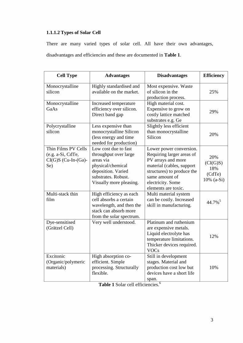
1.1.1.2 Types of Solar Cell
There are many varied types of solar cell. All have their own advantages,
disadvantages and efficiencies and these are documented in Table 1.
Table 1 Solar cell efficiencies.6
Cell Type Advantages Disadvantages Efficiency
Monocrystalline
silicon
Highly standardised and
available on the market.
Most expensive. Waste
of silicon in the
production process.
25%
Monocrystalline
GaAs
Increased temperature
efficiency over silicon.
Direct band gap
High material cost.
Expensive to grow on
costly lattice matched
substrates e.g. Ge
29%
Polycrystalline
silicon
Less expensive than
monocrystalline Silicon
(less energy and time
needed for production)
Slightly less efficient
than monocrystalline
Silicon 20%
Thin Films PV Cells
(e.g. a-Si, CdTe,
CI(G)S (Cu-In-(Ga)-
Se)
Low cost due to fast
throughput over large
areas via
physical/chemical
deposition. Varied
substrates. Robust.
Visually more pleasing.
Lower power conversion.
Requiring larger areas of
PV arrays and more
material (cables, support
structures) to produce the
same amount of
electricity. Some
elements are toxic.
20%
(CI(G)S)
18%
(CdTe)
10% (a-Si)
Multi-stack thin
film
High efficiency as each
cell absorbs a certain
wavelength, and then the
stack can absorb more
from the solar spectrum.
Multi material system
can be costly. Increased
skill in manufacturing. 44.7%
5
Dye-sensitised
(Grätzel Cell)
Very well understood. Platinum and ruthenium
are expensive metals.
Liquid electrolyte has
temperature limitations.
Thicker devices required.
VOCs
12%
Excitonic
(Organic/polymeric
materials)
High absorption co-
efficient. Simple
processing. Structurally
flexible.
Still in development
stages. Material and
production cost low but
devices have a short life
span.
10%
4
The work discussed within the scope of this research involves the potential
application of semiconductor materials in a p-n junction as a nanostructured solar
cell. The following sections briefly describe the background scientific theory
necessary to understand the motivation and objectives based upon the required
attributes of a PV device.
1.2 Band Theory
The electrical properties of a solid are determined by the distribution of electrons.
Band theory can be used to describe the electronic structure of conductors, insulators
and semiconductors.
1.2.1 Conductors
A conductor is a material in which electric current (i.e. electrons) flow under the
influence of an applied voltage. Metals are all conductors. Lithium (Li), is the
lightest metal, and contains atoms held together in a three-dimensional crystal
lattice. Bonding interactions among these atoms can be described by orbital overlap.
One Li atom contributes one s orbital at certain energy. When we introduce a second
atom, it overlaps the first and forms bonding and anti-bonding orbitals, three atoms
would have three molecular orbitals, n atoms would give n molecular orbitals. As
the number of atoms increases, the number of molecular orbitals covering a band of
energies increases, and the energy spacing between them decreases as the band
remains of finite width. For an infinite number of atoms, the orbitals are spaced so
closely that they behave as though they are merged together into an energy band.
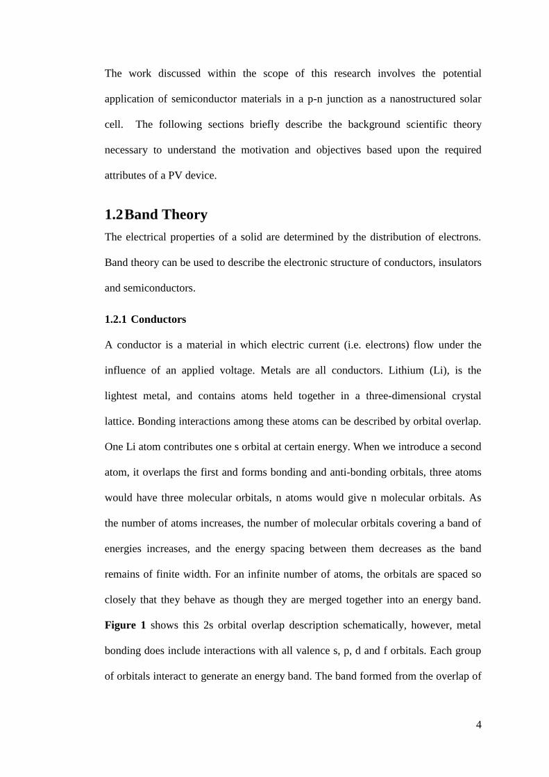
Figure 1 shows this 2s orbital overlap description schematically, however, metal
bonding does include interactions with all valence s, p, d and f orbitals. Each group
of orbitals interact to generate an energy band. The band formed from the overlap of
5
the s orbitals is called the s band. If the atoms have p orbitals available the same
procedure applies and leads to a p band.
Figure 1 Schematic view of band theory for the energies of delocalised orbitals
made from the 2s orbitals of lithium atoms. A metal containing n atoms of Lithium,
has a continuous band of filled bonding and empty antibonding orbitals. (adapted
from 7)
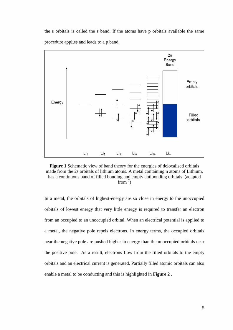
In a metal, the orbitals of highest-energy are so close in energy to the unoccupied
orbitals of lowest energy that very little energy is required to transfer an electron
from an occupied to an unoccupied orbital. When an electrical potential is applied to
a metal, the negative pole repels electrons. In energy terms, the occupied orbitals
near the negative pole are pushed higher in energy than the unoccupied orbitals near
the positive pole. As a result, electrons flow from the filled orbitals to the empty
orbitals and an electrical current is generated. Partially filled atomic orbitals can also
enable a metal to be conducting and this is highlighted in Figure 2 .
6
Figure 2 Idealized band structure of a metal, insulator and semi-conductor.8
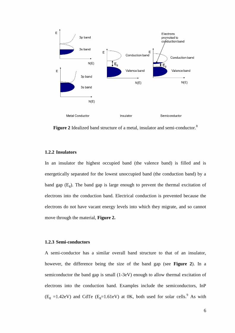
1.2.2 Insulators
In an insulator the highest occupied band (the valence band) is filled and is
energetically separated for the lowest unoccupied band (the conduction band) by a
band gap (Eg). The band gap is large enough to prevent the thermal excitation of
electrons into the conduction band. Electrical conduction is prevented because the
electrons do not have vacant energy levels into which they migrate, and so cannot
move through the material, Figure 2.
1.2.3 Semi-conductors
A semi-conductor has a similar overall band structure to that of an insulator,
however, the difference being the size of the band gap (see Figure 2). In a
semiconductor the band gap is small (1-3eV) enough to allow thermal excitation of
electrons into the conduction band. Examples include the semiconductors, InP
(Eg =1.42eV) and CdTe (Eg=1.61eV) at 0K, both used for solar cells.9 As with
7
molecular orbitals, the energy levels in a band are progressively filled from the
lowest energy upwards. At zero Kelvin, the electrons occupy only the lowest energy
levels available. The Fermi Level, Ef, refers to the highest occupied molecular
orbital at absolute zero, and will be discussed further in section 1.3. Above zero
Kelvin, electrons can be thermally excited to higher levels. Raising the temperature
of the semiconductor increases the number of electrons promoted across the band
gap. This is an important property of an intrinsic or un-doped semiconductor. The
number of electrons in the conduction band must equal the number of holes in the
valence band. (Note for a metal, increasing the temperature actually reduces the
conductivity due to increased thermal motion in the lattice which limits the electron
mobility due to increased collision between the lattice and electrons).
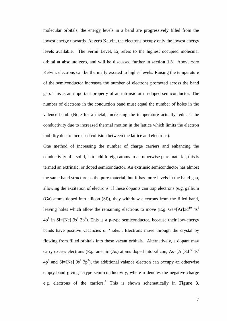
One method of increasing the number of charge carriers and enhancing the
conductivity of a solid, is to add foreign atoms to an otherwise pure material, this is
termed an extrinsic, or doped semiconductor. An extrinsic semiconductor has almost
the same band structure as the pure material, but it has more levels in the band gap,
allowing the excitation of electrons. If these dopants can trap electrons (e.g. gallium
(Ga) atoms doped into silicon (Si)), they withdraw electrons from the filled band,
leaving holes which allow the remaining electrons to move (E.g. Ga=[Ar]3d10
4s2
4p1 in Si=[Ne] 3s
2 3p
2). This is a p-type semiconductor, because their low-energy
bands have positive vacancies or ‘holes’. Electrons move through the crystal by
flowing from filled orbitals into these vacant orbitals. Alternatively, a dopant may
carry excess electrons (E.g. arsenic (As) atoms doped into silicon, As=[Ar]3d10
4s2
4p3 and Si=[Ne] 3s
2 3p
2), the additional valance electron can occupy an otherwise
empty band giving n-type semi-conductivity, where n denotes the negative charge
e.g. electrons of the carriers.7 This is shown schematically in Figure 3.
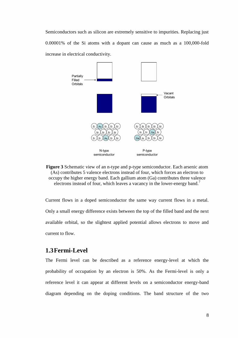
8
Semiconductors such as silicon are extremely sensitive to impurities. Replacing just
0.00001% of the Si atoms with a dopant can cause as much as a 100,000-fold
increase in electrical conductivity.
Figure 3 Schematic view of an n-type and p-type semiconductor. Each arsenic atom
(As) contributes 5 valence electrons instead of four, which forces an electron to
occupy the higher energy band. Each gallium atom (Ga) contributes three valence
electrons instead of four, which leaves a vacancy in the lower-energy band.7
Current flows in a doped semiconductor the same way current flows in a metal.
Only a small energy difference exists between the top of the filled band and the next
available orbital, so the slightest applied potential allows electrons to move and
current to flow.
1.3 Fermi-Level
The Fermi level can be described as a reference energy-level at which the
probability of occupation by an electron is 50%. As the Fermi-level is only a
reference level it can appear at different levels on a semiconductor energy-band
diagram depending on the doping conditions. The band structure of the two
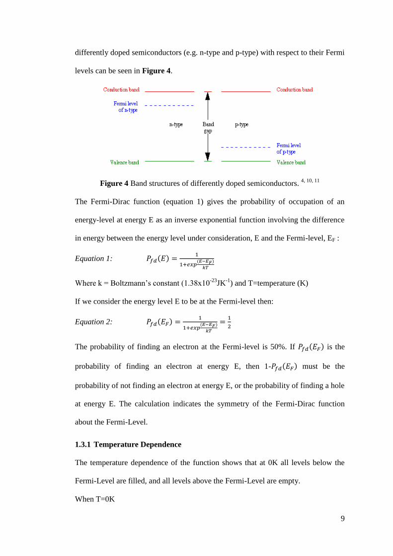
9
differently doped semiconductors (e.g. n-type and p-type) with respect to their Fermi
levels can be seen in Figure 4.
Figure 4 Band structures of differently doped semiconductors. 4, 10, 11
The Fermi-Dirac function (equation 1) gives the probability of occupation of an
energy-level at energy E as an inverse exponential function involving the difference
in energy between the energy level under consideration, E and the Fermi-level, EF :
Equation 1: ( )
( )
Where k = Boltzmann’s constant (1.38x10⁻²³
JK-1
) and T=temperature (K)
If we consider the energy level E to be at the Fermi-level then:
Equation 2: ( )
( )
The probability of finding an electron at the Fermi-level is 50%. If ( ) is the
probability of finding an electron at energy E, then 1- ( ) must be the
probability of not finding an electron at energy E, or the probability of finding a hole
at energy E. The calculation indicates the symmetry of the Fermi-Dirac function
about the Fermi-Level.
1.3.1 Temperature Dependence
The temperature dependence of the function shows that at 0K all levels below the
Fermi-Level are filled, and all levels above the Fermi-Level are empty.
When T=0K
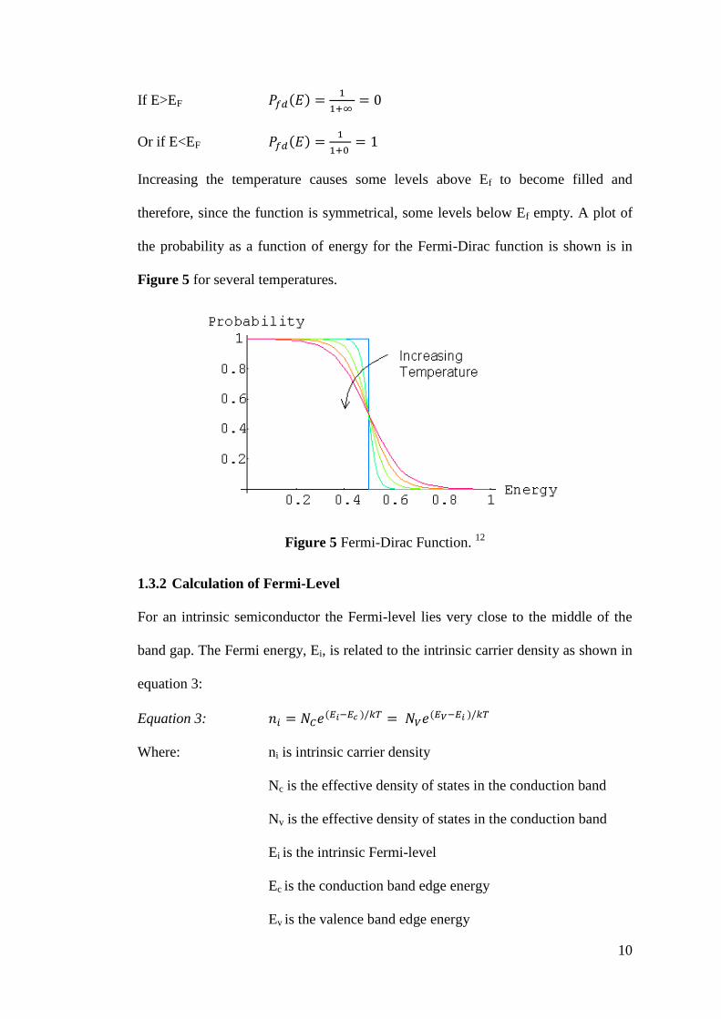
10
If E>EF ( )
Or if E<EF ( )
Increasing the temperature causes some levels above Ef to become filled and
therefore, since the function is symmetrical, some levels below Ef empty. A plot of
the probability as a function of energy for the Fermi-Dirac function is shown is in
Figure 5 for several temperatures.
Figure 5 Fermi-Dirac Function. 12
1.3.2 Calculation of Fermi-Level
For an intrinsic semiconductor the Fermi-level lies very close to the middle of the
band gap. The Fermi energy, Ei, is related to the intrinsic carrier density as shown in
equation 3:
Equation 3: ( )
( )
Where: ni is intrinsic carrier density
Nc is the effective density of states in the conduction band
Nv is the effective density of states in the conduction band
Ei is the intrinsic Fermi-level
Ec is the conduction band edge energy
Ev is the valence band edge energy
11
To eliminate the intrinsic Fermi energy from both of the above (equation 3),
multiply both Ei and take the square root. This now provides an expression for the
intrinsic carrier density as a function of the effective density of states in the
conduction and valence band (and thus the band gap energy as Eg=Ec-Ev):
Equation 4: √ ( )
Where: k=Boltzmann’s constant (1.38x10⁻²³
JK-1
)
T=temperature (K)
By rearrangement of equations 3 and 4, to calculate the position that the Fermi-level
occupies in an intrinsic, un-doped semiconductor:
Equation 5:
(
)
Knowing that the product of the electron and hole density (n and p respectively) is
equal to the square of the intrinsic carrier density
Equation 6: ( )
The intrinsic Fermi energy can also be expressed as a function of the effective
masses of the electrons and holes in the semiconductor. Using the expressions for
the effective density of states in the conduction and valence band (equation 5) and
combining with 6:
Equation 7:
Where: is the hole effective mass
is the electron effective mass
In general the electron and hole effective masses are unequal and therefore the
intrinsic Fermi-level does not lie in the exact middle of the band gap. The intrinsic
Fermi-level would lie in the middle of the band gap if T=0K as the part of the
equation containing the effective masses disappears.
12
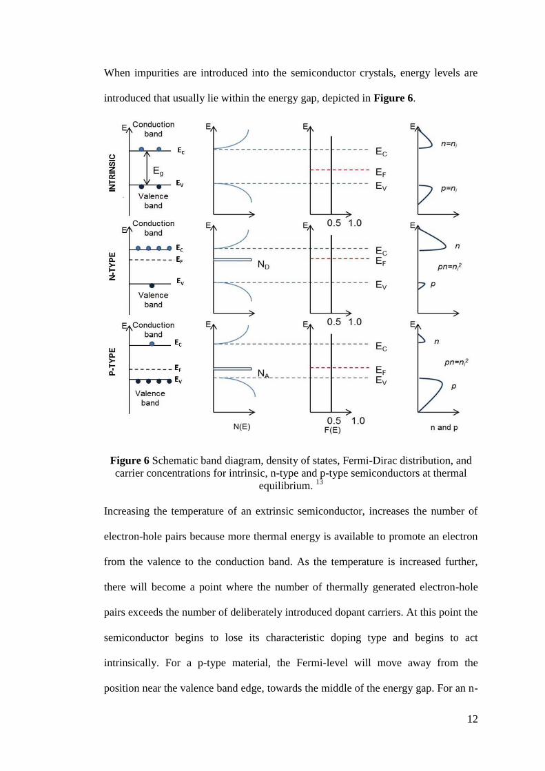
When impurities are introduced into the semiconductor crystals, energy levels are
introduced that usually lie within the energy gap, depicted in Figure 6.
Figure 6 Schematic band diagram, density of states, Fermi-Dirac distribution, and
carrier concentrations for intrinsic, n-type and p-type semiconductors at thermal
equilibrium. 13
Increasing the temperature of an extrinsic semiconductor, increases the number of
electron-hole pairs because more thermal energy is available to promote an electron
from the valence to the conduction band. As the temperature is increased further,
there will become a point where the number of thermally generated electron-hole
pairs exceeds the number of deliberately introduced dopant carriers. At this point the
semiconductor begins to lose its characteristic doping type and begins to act
intrinsically. For a p-type material, the Fermi-level will move away from the
position near the valence band edge, towards the middle of the energy gap. For an n-
13
type material, the Fermi-level moves away from the conduction band edge and
towards the middle of the gap with increasing temperature.
1.4 Band-gap Energy
Particles under certain conditions can show wave-like behaviour, one example of
this is when electrons (and holes) travelling through a crystal lattice are diffracted.
To link particle to wave-like behaviour, we can use the de Broglie equation to
calculate the wavelength, λ, of the electron. Electrons will only be diffracted if they
satisfy the diffraction condition which is a function of their momentum. For the
diffraction of waves (e.g. x-rays) the Bragg diffraction condition, equation 8, must
be obeyed:
Equation 8:
Where: n= order of diffraction
λ=the wavelength of X-rays
d=atomic spacing (lattice parameter)
θ=incident angle of the incoming X-Rays
Assuming wave propagation is normal to a set of atomic planes, the angular
dependence is neglected, when thinking about the diffraction of particles (e.g.
electrons), the angle free diffraction equation becomes:
Equation 9:
At values of λ given in equation 9, standing waves will be set-up between the atomic
planes. Since the wavelength of the electron is directly related to its momentum,
electrons with this momentum cannot propagate through the crystal lattice and the
velocity is zero. These conditions account for forbidden energy bands. If there was a
completely free electron, its energy is related to its momentum by:
14
Equation 10:
Where: E=energy
p=momentum
m=mass of electron
Writing the momentum in terms of the particles de Broglie wavelength:
Equation 11:
Where: h=Planck’s constant
Knowing that the propagation constant of a wave is denoted by k, where
Equation 12:
The energy-momentum equation can now become:
Equation 13:
Where: =h/2π
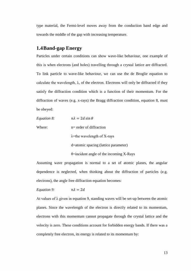
Equation 13 now relates the energy of a particle, E, with the propagation constant, k,
and this is shown graphically in Figure 7.
Figure 7 Energy-momentum diagram for a free electron. 12, 14
The E-k curve is parabolic and all values of energy (and momentum) are allowed.
To find the mass of the particle, (given in the E-k diagram the mass is inversely
proportional to the curvature of the E-k curve),
15
Equation 14:
Equation 15:
Equation 16:
Although this was generated assuming free electrons, the equation still holds for
electrons (or holes) in crystals, so more generally the effective mass of the particle
(electron or hole), m*, can be calculated using:
Equation 17:
⁄
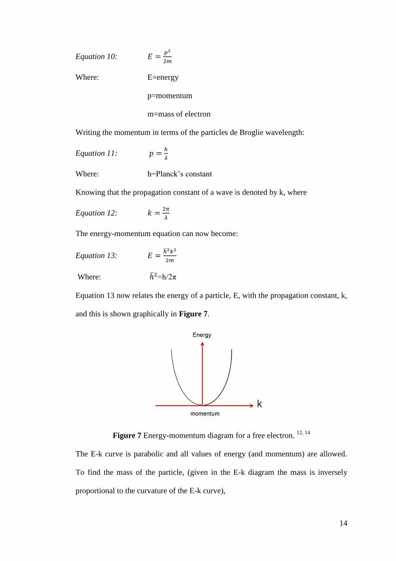
As explained earlier, the band-gap energy is defined as the difference in energy
between the valence and conduction bands for insulators and semiconductors. The
band-gap can be further categorized as direct or indirect. Figure 8 shows two
hypothetical energy-momentum diagrams for a direct and indirect band-gap
semiconductor.
Figure 8 Energy-momentum diagrams for a semiconductor. 15
16
For an indirect band gap semiconductor, note that there is a maximum in the valence
band curve at k=0, and a minimum in the conduction band curve at a different k
value. If an electron sitting near the conduction band minimum (where its energy is
lowest) is to recombine with a hole sitting near the valance band maximum, then the
electron must lose some momentum in making this transition. To ensure the overall
momentum is conserved a phonon is released. Conversely, for a direct band gap
semiconductor when k=0 the conduction band is at a minimum and the valence band
is at a maximum. This means that an electron and hole pair can recombine and there
is no change in momentum required.
III-V semiconductors (e.g. GaAs) are direct band-gap materials with efficient photon
producers which makes them suitable for use in LEDs and LASERs, whilst bulk
silicon is a highly inefficient photon producer and is an indirect band gap material.
1.5 Carrier Concentration and Mobility
The conductivity of a semi-conductor is determined by both the carrier concentration
and the electron mobility (µ). The carrier concentration is the number of electrons or
holes per unit area and the electron mobility is simply the ratio of the drift velocity
and the electric field, and relates to the ease of movement of the carriers under the
effect of an electric field. Both these features are highly influenced by temperature;
at higher temperature, higher lattice vibrations allow energy to transfer between the
lattice and carriers thus leading to scattering and reduced mobility. At higher
temperatures for an intrinsic semiconductor, more electron-hole pairs are generated
so the conductivity increases, eventually, the semiconductor breaks down.
17
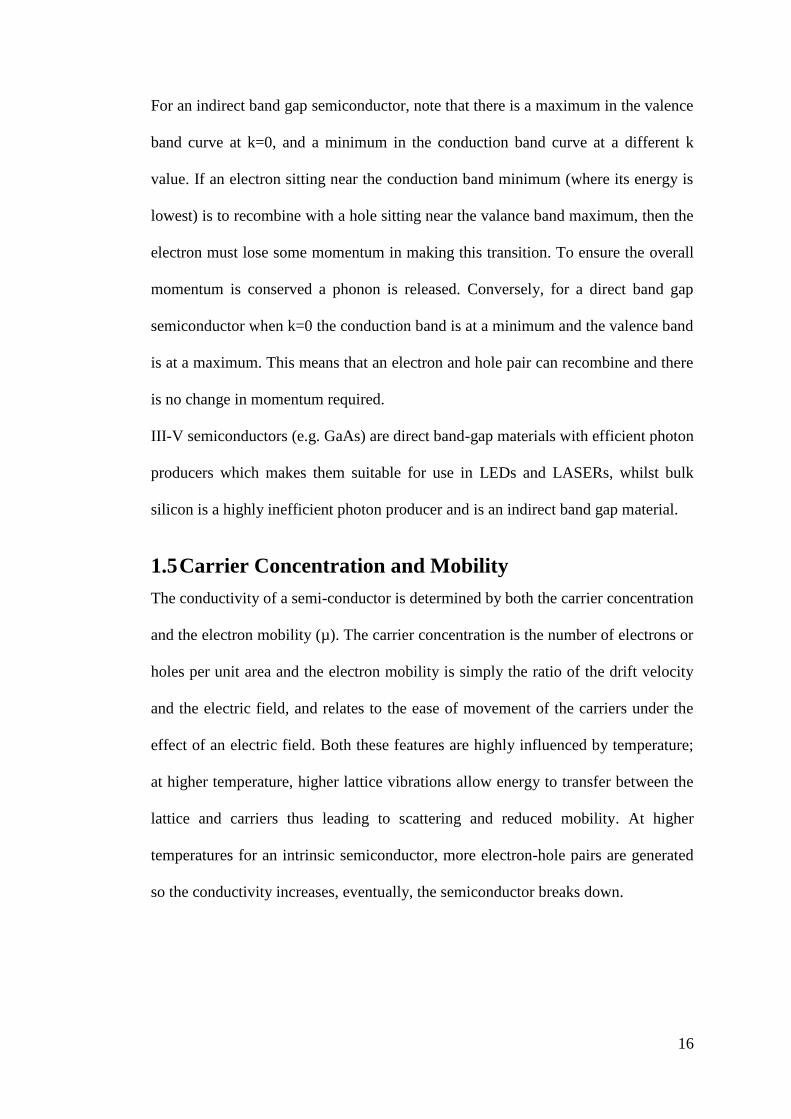
1.6 The p-n junction
The p-n junction is of great importance both in modern electronic applications and
in understanding other semi-conductor devices. When a p-type and n-type material
are placed in contact with one another, it allows current to flow easily in one
direction only (forward biased) and not in the other (reverse biased), creating a
diode. This non-reversing behaviour comes from the charge transport process in the
two types of material. Figure 9 shows a schematic of an idealised p-n junction.
Figure 9 Idealised p-n junction. 12
A p-type material (rich in holes) has formed a junction with an n-type material (rich
in electrons), with the solid line in Figure 9 representing the junction. The holes and
the electrons ideally would like to recombine. Due to the charges of the holes and
electrons the conditions are ideal for diffusion of the holes towards the electron (i.e.
from the right hand side of the junction to the left) and vice-versa. The material
gains its p- or n-type characteristic due to its doping with donor and accepting
elements that are held in fixed positions in the lattice (unless the semiconductor is
heated and they can then diffuse). The electrons and holes from the donor and
acceptor atoms are free to move. As the holes diffuse to the left side of the junction
to combine with electrons, negative charges are left behind. Similarly, electron
18
moving from the left to the right will leave behind positive donor centres. An
equilibrium condition is reached as shown in Figure 9 in the region between the two
dotted lines. This region can be termed the depletion region, (i.e. it is depleted of
charge carriers). It is worth noting that the fixed charges builds up to a point where
the electric field produced slows down the diffusion process. Away from the
junction region, the material has no charge as the carriers still sit on the dopant
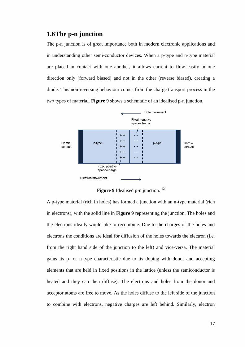
centres. When the p and n type materials are brought together at thermal
equilibrium, the Fermi levels on either side are forced to align, causing the valence
and conduction bands to bend as shown Figure 10.
Figure 10 A p-n junction energy diagram. 11, 12
The overriding factor is that the Fermi-level has to remain continuous at a junction.
This then allows the movement of electrons and holes, which creates charge
depletion regions and an altered band structure. In thermal equilibrium there is zero
net current flow as the opposing drift and diffusion currents cancel each other out.
Under non-thermal equilibrium conditions e.g. when a voltage is applied, one of the
19
current flow mechanisms dominates, resulting in a net-current flow in one direction.
From looking at the diagram, the electrons diffusing from the n-type to the p-type
have to overcome the potential barrier of the conduction band. A voltage (bias) can
be applied to a junction by connecting the positive terminal of the voltage source to
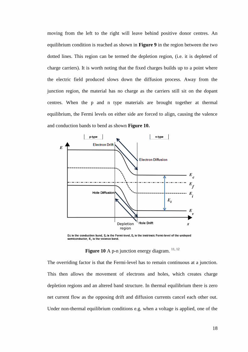
the n-side or p-side of the junction. The basic theory of current-voltage
characteristics of p-n junctions was established by Shockley.16, 17
This theory was
then extended by Sah, Noyce and Shockely.18, 19
Figure 11 shows the p-n junction
current and voltage, I-V characteristics.
Figure 11 Current and voltage characteristics of a p-n junction. 20
From looking at Figure 11 it is evident that current flows easily in one direction
(forward bias) and little current flow in reverse bias. The current increases
exponentially in the forward direction whilst for the reverse the current is low and
constant until breakdown. For forward bias, the positive terminal is connected to the
p-type material and the negative to the n-type. The holes in the p-type region and the
electrons in the n-type region are pushed towards the junction. As the applied
voltage increases, the depletion zone eventually becomes narrow enough that
20
electrons can cross the junction. The electrons penetrate only a short distance into
the p-type material, as it is energetically favourable for them to recombine with
holes. The electric current continues to flow as holes begin to move in the opposite
direction.
For reverse bias, the negative terminal is contacted to the p-type material and the
positive is terminal is contacted to the n-type material. In the p-type material the
holes move towards the terminal of the power supply and away from the junction.
For the n-type material, the electrons are drawn towards the positive terminal. The
width of the depletion zone increases. This results in a higher resistance to the
movement of charge carries, and thus the current generated is minimal, the p-n
junction now behaves more like an insulator.
1.6.1 A p-n junction solar cell
Applications in which p-n junctions are incorporated into technology in the modern
world include diodes, transistors, LEDs and photodetectors. The following text,
together with Figure 12 provides more detail on the mechanism and involvement of
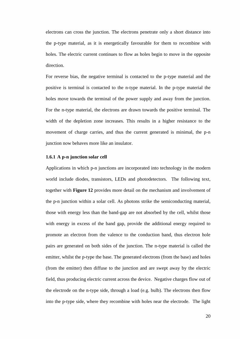
the p-n junction within a solar cell. As photons strike the semiconducting material,
those with energy less than the band-gap are not absorbed by the cell, whilst those
with energy in excess of the band gap, provide the additional energy required to
promote an electron from the valence to the conduction band, thus electron hole
pairs are generated on both sides of the junction. The n-type material is called the
emitter, whilst the p-type the base. The generated electrons (from the base) and holes
(from the emitter) then diffuse to the junction and are swept away by the electric
field, thus producing electric current across the device. Negative charges flow out of
the electrode on the n-type side, through a load (e.g. bulb). The electrons then flow
into the p-type side, where they recombine with holes near the electrode. The light
21
energy originally absorbed by the electrons is used up while the electrons power the
external circuit, thus, equilibrium is maintained.21
The incident light continually
creates more electron-hole pairs and, more charge imbalance, the charge imbalance
is relieved by the current which gives up energy in performing work.3 This is shown
schematically in Figure 12.
Figure 12 Carrier generation and current flow at the junction. 1, 11, 22
Each semiconductor has its own band gap which means it can only convert certain
parts of the solar spectrum. As all the generated electron-hole pairs have energy in
excess of the band gap, immediately after their creation, the electron and hole decay
to states near the edges of their respective bands. The excess energy is lost as heat
and cannot be converted into useful power. This represents one of the fundamental
loss mechanisms in a solar cell.
The generation and recombination of electron hole pairs control cell efficiency. The
quantum efficiency (QE) or spectral response of a cell is given by:
Equation 18: ( )
Where: ( ) is the ratio between the number of charge carriers the
cell yields and the number of photon illuminating the cell for a given unit of time.
22
If ( ) for a given solar cell is known then the maximum theoretical current
density of the cell can be calculated for any given incident spectrum according to
Equation 19: ∫ ( ) ( )
Where: q=electron charge
λ=wavelength (where λ0 and λ1 are the limits of the
wavelength range within which the cell shows photo-activity)
=the flux of the spectrum illuminating the cell which in turn
can be calculated by:
Equation 20: ( ) ( )
( )
Where: P(λ) is the spectral irradiance
E(λ) is the photon energy given by E=hc/λ.
These equations allow an estimation of the upper limit of current generation in PV
cells.23
The efficiency (n) of a solar cell is defined as the power Pmax supplied by the
cell at the maximum power point under standard test conditions, divided by the
power of the radiation incident upon it. Most frequent conditions for testing cell
efficiency include an irradiance value of 100 mW/cm2 with a standard reference
spectrum, at a temperature of 25°C. The use of this standard is particularly
convenient since the cell efficiency in per cent is then numerically equal to the
power output from the cell in mW/cm2. (Refer back to Table 1).
1.6.2 Target PV cell.
The theory and design of PV cells is too vast to include here. A brief summary for
the constituents required for a functioning cell are summarised in the following text,
with an indication for further reading given by the references. Although this thesis
looks to material development, Figure 13 highlights the two proposed structures for
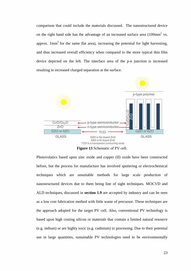
23
comparison that could include the materials discussed. The nanostructured device
on the right hand side has the advantage of an increased surface area (100mm2 vs.
approx. 1mm2
for the same flat area), increasing the potential for light harvesting,
and thus increased overall efficiency when compared to the more typical thin film
device depicted on the left. The interface area of the p-n junction is increased
resulting in increased charged separation at the surface.
Figure 13 Schematic of PV cell.
Photovolatics based upon zinc oxide and copper (II) oxide have been constructed
before, but the process for manufacture has involved sputtering or electrochemical
techniques which are unsuitable methods for large scale production of
nanostructured devices due to them being line of sight techniques. MOCVD and
ALD techniques, discussed in section 1.9 are accepted by industry and can be seen
as a low cost fabrication method with little waste of precursor. These techniques are
the approach adopted for the target PV cell. Also, conventional PV technology is
based upon high costing silicon or materials that contain a limited natural resource
(e.g. indium) or are highly toxic (e.g. cadmium) in processing. Due to their potential
use in large quantities, sustainable PV technologies need to be environmentally
24
friendly, manufactured from a metal that has a vast natural resources, are of low-cost
to process and be able to absorb and wide range of the solar spectrum and be durable
to solar radiation . Many metal oxide semiconductors are n-type in nature e.g. ZnO.
Only a few p-type oxide semiconductors exist, and these include both CuO and
Cu2O. The aim of this thesis was to investigate these materials with a view for their
incorporation into a nanostructured PV cell as structurally and electronically
compatible layers enabling the absorption of a wide range of solar radiation.
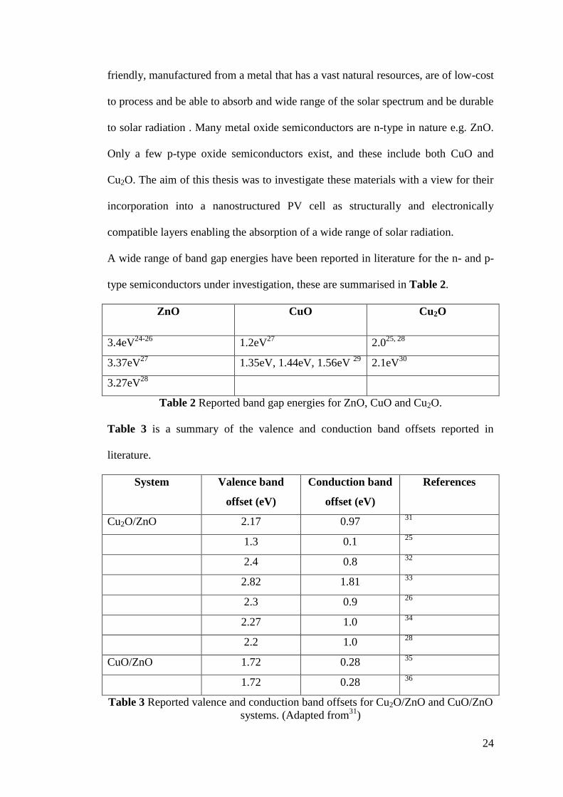
A wide range of band gap energies have been reported in literature for the n- and p-
type semiconductors under investigation, these are summarised in Table 2.
ZnO CuO Cu2O
3.4eV24-26
1.2eV27
2.025, 28
3.37eV27
1.35eV, 1.44eV, 1.56eV 29
2.1eV30
3.27eV28
Table 2 Reported band gap energies for ZnO, CuO and Cu2O.
Table 3 is a summary of the valence and conduction band offsets reported in
literature.
System Valence band
offset (eV)
Conduction band
offset (eV)
References
Cu2O/ZnO 2.17 0.97 31
1.3 0.1 25
2.4 0.8 32
2.82 1.81 33
2.3 0.9 26
2.27 1.0 34
2.2 1.0 28
CuO/ZnO 1.72 0.28 35
1.72 0.28 36
Table 3 Reported valence and conduction band offsets for Cu2O/ZnO and CuO/ZnO
systems. (Adapted from31
)
25
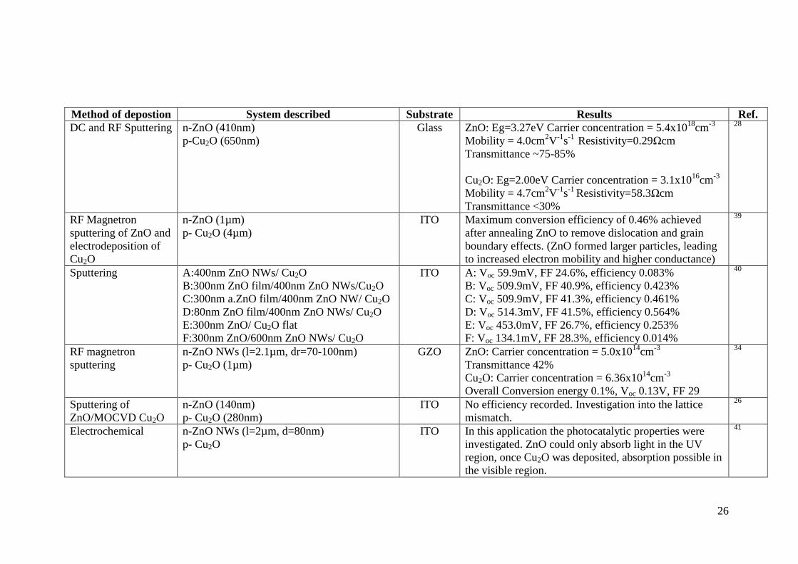
The deposition of a p-n junction involving the zinc and copper oxide materials via
ALD and CVD methods is lacking from literature, highlighting the novelty of the
aim of the thesis. For reference, some of the techniques that have been successfully
employed in the deposition of the ZnO/CuO/Cu2O systems are discussed in Table 4
to provide an insight into material properties. Generally, the efficiency is reported as
less than 0.5% due to poor interface quality and interface defects,37
although Mittiga
et al. report a 2% efficiency for an ZnO/Cu2O solar cell from sputtering and thermal
methods.38
The substrates and transparent conducting oxides will be discussed in
section 1.7 and 1.8, followed by deposition techniques in section 1.9. The concept
of nanowires (NWs) will be covered in Chapter 2.
26
Method of depostion System described Substrate Results Ref.
DC and RF Sputtering n-ZnO (410nm)
p-Cu2O (650nm)
Glass ZnO: Eg=3.27eV Carrier concentration = 5.4x10¹⁸
cm-3
Mobility = 4.0cm2V
-1s
-1 Resistivity=0.29Ωcm
Transmittance ~75-85%
Cu2O: Eg=2.00eV Carrier concentration = 3.1x10¹⁶
cm-3
Mobility = 4.7cm2V
-1s
-1 Resistivity=58.3Ωcm
Transmittance <30%
28
RF Magnetron
sputtering of ZnO and
electrodeposition of
Cu2O
n-ZnO (1µm)
p- Cu2O (4µm)
ITO Maximum conversion efficiency of 0.46% achieved
after annealing ZnO to remove dislocation and grain
boundary effects. (ZnO formed larger particles, leading
to increased electron mobility and higher conductance)
39
Sputtering A:400nm ZnO NWs/ Cu2O
B:300nm ZnO film/400nm ZnO NWs/Cu2O
C:300nm a.ZnO film/400nm ZnO NW/ Cu2O
D:80nm ZnO film/400nm ZnO NWs/ Cu2O
E:300nm ZnO/ Cu2O flat
F:300nm ZnO/600nm ZnO NWs/ Cu2O
ITO A: Voc 59.9mV, FF 24.6%, efficiency 0.083%
B: Voc 509.9mV, FF 40.9%, efficiency 0.423%
C: Voc 509.9mV, FF 41.3%, efficiency 0.461%
D: Voc 514.3mV, FF 41.5%, efficiency 0.564%
E: Voc 453.0mV, FF 26.7%, efficiency 0.253%
F: Voc 134.1mV, FF 28.3%, efficiency 0.014%
40
RF magnetron
sputtering
n-ZnO NWs (l=2.1µm, dr=70-100nm)
p- Cu2O (1µm)
GZO ZnO: Carrier concentration = 5.0x10¹⁴
cm-3
Transmittance 42%
Cu2O: Carrier concentration = 6.36x10¹⁴
cm-3
Overall Conversion energy 0.1%, Voc 0.13V, FF 29
34
Sputtering of
ZnO/MOCVD Cu2O
n-ZnO (140nm)
p- Cu2O (280nm)
ITO No efficiency recorded. Investigation into the lattice
mismatch.
26
Electrochemical n-ZnO NWs (l=2µm, d=80nm)
p- Cu2O
ITO In this application the photocatalytic properties were
investigated. ZnO could only absorb light in the UV
region, once Cu2O was deposited, absorption possible in
the visible region.
41
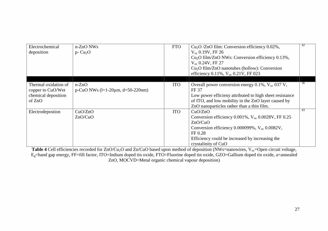
27
Electrochemical
deposition
n-ZnO NWs
p- Cu2O
FTO Cu2O /ZnO film: Conversion efficiency 0.02%,
Voc 0.19V, FF 26
Cu2O film/ZnO NWs: Conversion efficiency 0.13%,
Voc 0.24V, FF 27
Cu2O film/ZnO nanotubes (hollow): Conversion
efficiency 0.11%, Voc 0.21V, FF 023
42
Thermal oxidation of
copper to CuO/Wet
chemical deposition
of ZnO
n-ZnO
p-CuO NWs (l=1-20µm, d=50-220nm)
ITO Overall power conversion energy 0.1%, Voc 037 V,
FF 37
Low power efficieny attributed to high sheet resistance
of ITO, and low mobility in the ZnO layer caused by
ZnO nanoparticles rather than a thin film.
36
Electrodepostion CuO/ZnO
ZnO/CuO
ITO CuO/ZnO
Conversion efficiency 0.001%, Voc 0.0028V, FF 0.25
ZnO/CuO
Conversion efficiency 0.000099%, Voc 0.0082V,
FF 0.28
Efficiency could be increased by increasing the
crystalinity of CuO
43
Table 4 Cell efficiencies recorded for ZnO/Cu2O and Zn/CuO based upon method of deposition (NWs=nanowires, Voc=Open circuit voltage,
Eg=band gap energy, FF=fill factor, ITO=Indium doped tin oxide, FTO=Fluorine doped tin oxide, GZO=Gallium doped tin oxide, a=annealed
ZnO, MOCVD=Metal organic chemical vapour deposition)
28
1.7 Substrate
Referring back to Figure 13, the substrate used is glass as it is transparent and can
allow the incident light to penetrate into the device. The research undertaken
investigated a variety of substrates during deposition to help gain an understanding
of growth mechanisms, composition and the impact of substrate on nucleation
density. A brief description of each of the substrates used in given in the following
text.
1.7.1 Glass
Glass has an extensive range of applications from architectural glazing and optics, to
food containers. During manufacture, the properties of glass e.g. colour and thermal
expansion can be tailored by adding alternative minerals. The large-scale glass
manufacturing process for flat glass is termed the ‘float glass’ process and was
introduced by Pilkington’s Glass.44
Glass is based on SiO2 but often contains
carefully controlled concentrations of other element oxides e.g. B, Ca, Mg, and Al,
to control the desired mechanical properties. The surface is hydroxyl terminated (Si-
OH bonds are formed from the reaction of the SiO2 with moisture in the atmosphere)
which makes it reactive towards further processing. Surface modification of glass
via thin film coatings is a widely used industrial technique and has the advantage of
altering surface chemical and physical properties while preserving the bulk. It often
takes place ‘off-line’ in that it is a separate process that takes place after
manufacture. CVD has been integrated into the glass industry to coat large areas of a
large range of high purity thin films uniformly; this is relevant to the target device,
as the TCO layer can be applied in this way.
29
1.7.2 Si(100) and Si(111)
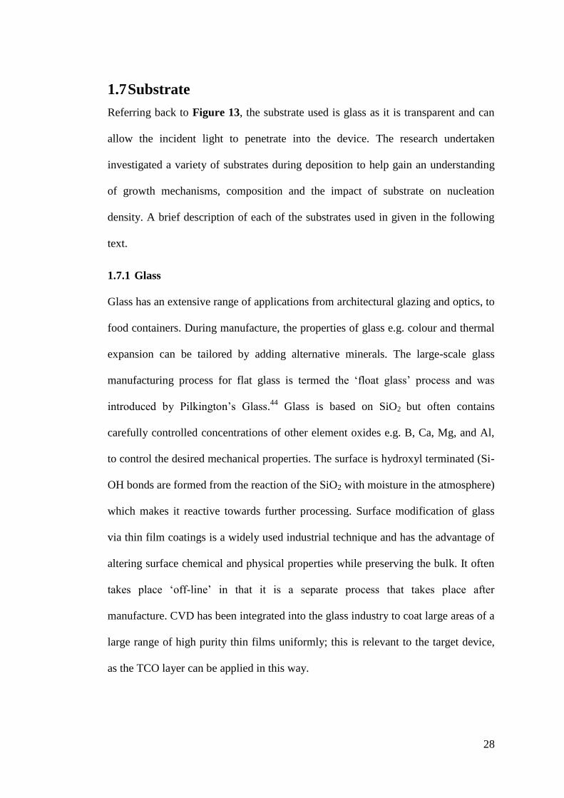
Silicon substrates were employed as they are well defined in terms of crystal
structure, optical property and surface smoothness. The supplied wafers were
100mm diameter from Compart Technology Ltd, Virgin Test Grade. Si(100) was
predominantly used for the copper deposition, whilst both Si(111) and Si(100) were
used for zinc oxide nanowire work. The face centred cubic crystal structure of
silicon is shown in Figure 14 with the direction of the 111 and 100 planes
highlighted.
Figure 14 The crystal structure of siliconwith (100) and (111) planes highlighted. 45
Silicon is prone to surface oxidation when exposed to air. The substrates were used
as supplied and a 20Å silicon dioxide layer was assumed. Ellipsometery was used
for measuring film thickness. The silicon used was heavily n-doped and was
therefore not suitable for electrical conductivity measurements. To accommodate
this, soda lime glass microscope slides (75mm x 25mm) were also used as
substrates. This also aided in the visual inspection of films to look for transparency,
uniformity and if reflective metallic films where deposited. Films grown on glass
provided thickness measurements based upon weight gain.
30
1.7.3 Titanium Nitride
Titanium nitride (TiN) is used as an adhesion layer and was used as a substrate to
help study copper deposition. Copper metal formed part of this research due to the
potential application of ALD copper as interconnect material in electronic devices.
A more complete discussion can be found in section 2.2.2.2.
1.7.4 Plastic
A plastic substrate named Mellinex® 505 was used for the copper deposition work.
This substrate has a thermal budget limited to 75°C, and was used to understand
how suitable the low temperature copper deposition process was to flexible
substrates, a current focus of the electronics industry.
1.8 Transparent Conducting Oxide
As glass is a non-conducting substrate, to enable an electrical contact (electrode) for
the hypothesised PV cell, a transparent conducting oxide (TCO) is used. TCOs are
used for many other applications including displays, circuitries and opto-electrical
interfaces. A TCO is usually made from a semiconductor material which can absorb
light at energies greater than the band gap energy, therefore semiconductors with
band gaps greater than the highest energy visible light (approximately 3.0eV) will be
transparent. TCOs enable light to pass through, with greater than 80% transmittance
of incident light. TCO extracts photogenerated electrons and transfers them to
external circuits. The conductivity can be tuned from insulating via semiconducting
to conducting via doping and can have conductivities >103 S/cm for efficient carrier
transport.46
31
1.8.1 Indium Tin Oxide (ITO)
Indium oxide is a wide band gap semiconductor (Eg=3.75eV). Doping with tin (n-
type) gives indium tin oxide (ITO), typically 90%wt In2O3, 10%wtSnO2. ITO is the
most widely used TCO as it has a high visible transmittance (>90%) and good
resistivity.47
The resistivity is related to the carrier concentration and mobility,
which in turn is related to dopant levels and oxygen vacancies, crystalinity, film
thickness and purity.48-51
Introducing tin initially increases the conductivity by
providing spare electrons, however at high dopant levels, scattering of charge
carriers can occur reducing the charge carrier mobility and thus, overall
conductivity. The highest conductivities are seen with 5-10at.% Sn. Precursors used
for the deposition of ITO include tin tetrachloride and indium β-diketonate
complexes. The deposition processes include, but are not limited to, electron beam
evaporation,52-54
magnetron sputtering,55, 56
thermal evaporation and pulsed laser
deposition.57
1.8.2 Fluorine doped Tin Oxide (FTO)
The majority of research on zinc oxide nanowire based solar cells has used fluorine
doped tin-oxide as the TCO material.58-60
However, the small difference in work
function of ZnO (5.1-5.3eV) 61, 62
and FTO (4.9eV) 63, 64
does not provide sufficient
driving force for the charge injection, leading to the need to look for an improved
TCO for this application.
1.8.3 Aluminium doped Zinc Oxide (AZO)
Aluminium doped (n-type) zinc oxide thins films, AZO, contain about 2%wt
aluminium and can be produced by spray pyrolysis,65, 66
sol gel technology,67-69
sputtering,70-73
ALD74
and CVD.75, 76
Nishino et report the deposition of AZO at
500°C via CVD using bis(2,4-pentanedionato) zinc and tris(2,4-
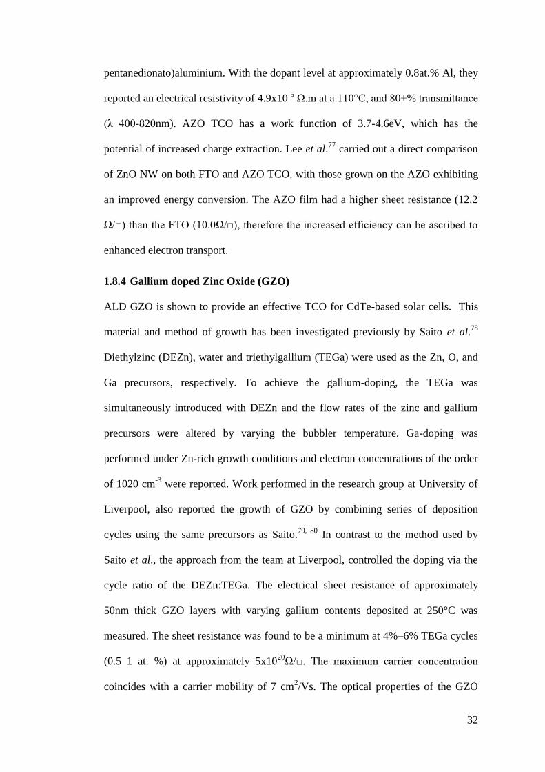
32
pentanedionato)aluminium. With the dopant level at approximately 0.8at.% Al, they
reported an electrical resistivity of 4.9x10⁻⁵
Ω.m at a 110°C, and 80+% transmittance
(λ 400-820nm). AZO TCO has a work function of 3.7-4.6eV, which has the
potential of increased charge extraction. Lee et al.77
carried out a direct comparison
of ZnO NW on both FTO and AZO TCO, with those grown on the AZO exhibiting
an improved energy conversion. The AZO film had a higher sheet resistance (12.2
Ω/) than the FTO (10.0Ω/), therefore the increased efficiency can be ascribed to
enhanced electron transport.
1.8.4 Gallium doped Zinc Oxide (GZO)
ALD GZO is shown to provide an effective TCO for CdTe-based solar cells. This
material and method of growth has been investigated previously by Saito et al.78
Diethylzinc (DEZn), water and triethylgallium (TEGa) were used as the Zn, O, and
Ga precursors, respectively. To achieve the gallium-doping, the TEGa was
simultaneously introduced with DEZn and the flow rates of the zinc and gallium
precursors were altered by varying the bubbler temperature. Ga-doping was
performed under Zn-rich growth conditions and electron concentrations of the order
of 1020 cm-3
were reported. Work performed in the research group at University of
Liverpool, also reported the growth of GZO by combining series of deposition
cycles using the same precursors as Saito.79, 80
In contrast to the method used by
Saito et al., the approach from the team at Liverpool, controlled the doping via the
cycle ratio of the DEZn:TEGa. The electrical sheet resistance of approximately
50nm thick GZO layers with varying gallium contents deposited at 250°C was
measured. The sheet resistance was found to be a minimum at 4%–6% TEGa cycles
(0.5–1 at. %) at approximately 5x10²⁰Ω/. The maximum carrier concentration
coincides with a carrier mobility of 7 cm2/Vs. The optical properties of the GZO
33
films were assessed by UV–vis spectrophotometry and the transmissions of the films
were approximately 80% in the visible spectrum. The ALD GZO was incorporated
into a Cd1-xZnxS/CdTe device structure, grown using the atmospheric pressure
metalorganic chemical vapour deposition (MOCVD) process described elsewhere.81
Cd1-xZnxS/CdTe photovoltaic cells deposited on GZO/glass substrates yielded a
quantum efficiency of 10.8% which is comparable to cell grown on industry
supplied TCO. Overall, GZO shows huge promise for use as a TCO in thin film
CdTe PV devices. Due to the lower sheet resistance of GZO materials than AZO
materials, the aim is to include GZO as the TCO for the PV cells depicted in
Figure 13.
1.9 Film Deposition Techniques
Many of the major scientific and technological advances have been made possible
due to substantial advances in the development and optimisation of thin film
deposition techniques. There is a range of methodologies suited to film formation
including physical vapour deposition (PVD), chemical vapour deposition (CVD) and
atomic layer deposition (ALD).
1.9.1 Physical Vapour Deposition
The term physical vapour deposition (PVD) covers a wide variety of techniques in
which a target material is evaporated under high vacuum and the resulting vapour
deposited on a substrate surface. A high vacuum is used to eliminate trace element
impurities, and often in-situ techniques such as Auger electron microscopy analysis
can be used during deposition. The method of evaporation can be via electron beam,
laser ablation and sputtering (magnetron and ion beam).82-84
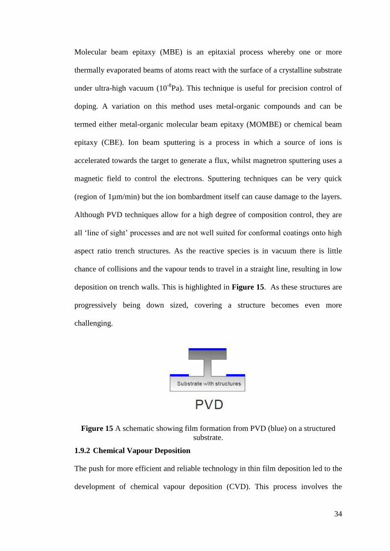
34
Molecular beam epitaxy (MBE) is an epitaxial process whereby one or more
thermally evaporated beams of atoms react with the surface of a crystalline substrate
under ultra-high vacuum (10-8
Pa). This technique is useful for precision control of
doping. A variation on this method uses metal-organic compounds and can be
termed either metal-organic molecular beam epitaxy (MOMBE) or chemical beam
epitaxy (CBE). Ion beam sputtering is a process in which a source of ions is
accelerated towards the target to generate a flux, whilst magnetron sputtering uses a
magnetic field to control the electrons. Sputtering techniques can be very quick
(region of 1µm/min) but the ion bombardment itself can cause damage to the layers.
Although PVD techniques allow for a high degree of composition control, they are
all ‘line of sight’ processes and are not well suited for conformal coatings onto high
aspect ratio trench structures. As the reactive species is in vacuum there is little
chance of collisions and the vapour tends to travel in a straight line, resulting in low
deposition on trench walls. This is highlighted in Figure 15. As these structures are
progressively being down sized, covering a structure becomes even more
challenging.
Figure 15 A schematic showing film formation from PVD (blue) on a structured
substrate.
1.9.2 Chemical Vapour Deposition
The push for more efficient and reliable technology in thin film deposition led to the
development of chemical vapour deposition (CVD). This process involves the
35
formation of a thin solid film on a substrate material by thermal decomposition of a
chemical precursor which can occur both in the gas phase and on the substrate. One
of the more commonly used CVD processes is metal-organic vapour phase epitaxy
(MOVPE), which produces single crystal films on single crystal substrates from
metal-organic precursors. CVD reactions are commonly assisted by using heat
(thermal CVD), plasma (Plasma Enhanced CVD, PECVD) or higher frequency
radiation (photo-assisted CVD). PECVD is a technique in which electrical energy is
used to generate chemically active ions and radicals. These then participate in the
heterogeneous reactions leading to deposition on the substrate. The advantage of
plasma CVD is that deposition can occur at very low temperatures, enabling
temperature sensitive substrates to be used. Other processes may involve the use of
high vacuum, or may be at atmospheric pressure.
MOCVD is a specific CVD process that utilizes metal-organic (organometallic)
precursors, and was pioneered by Manasevit in 1968.85
An organometallic precursor
is defined as a compound that contains a direct metal-carbon bond, however, due to
the varied nature of the precursors used in MOCVD, there is an inclusion of
precursors containing metal-oxygen, metal-nitrogen and metal-hydrogen bonds.
Materials deposited by MOCVD include metals, oxides, nitrides and sulphides. The
initial use of CVD included the blanket coverage of cutting tools to improve
performance and prolong life. Now, MOCVD is widely used in the microelectronics
industry. It forms part of the fabrication of semiconductor devices to deposit various
films including, polycrystalline, amorphous and epitaxal silicon and high-K
dielectrics. MOCVD is a technique which lends itself to end-use applications such
as solar cells, glass coatings, and medical devices.
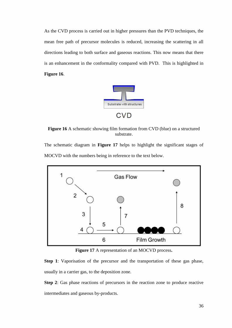
36
As the CVD process is carried out in higher pressures than the PVD techniques, the
mean free path of precursor molecules is reduced, increasing the scattering in all
directions leading to both surface and gaseous reactions. This now means that there
is an enhancement in the conformality compared with PVD. This is highlighted in
Figure 16.
Figure 16 A schematic showing film formation from CVD (blue) on a structured
substrate.
The schematic diagram in Figure 17 helps to highlight the significant stages of
MOCVD with the numbers being in reference to the text below.
Figure 17 A representation of an MOCVD process.
Step 1: Vaporisation of the precursor and the transportation of these gas phase,
usually in a carrier gas, to the deposition zone.
Step 2: Gas phase reactions of precursors in the reaction zone to produce reactive
intermediates and gaseous by-products.
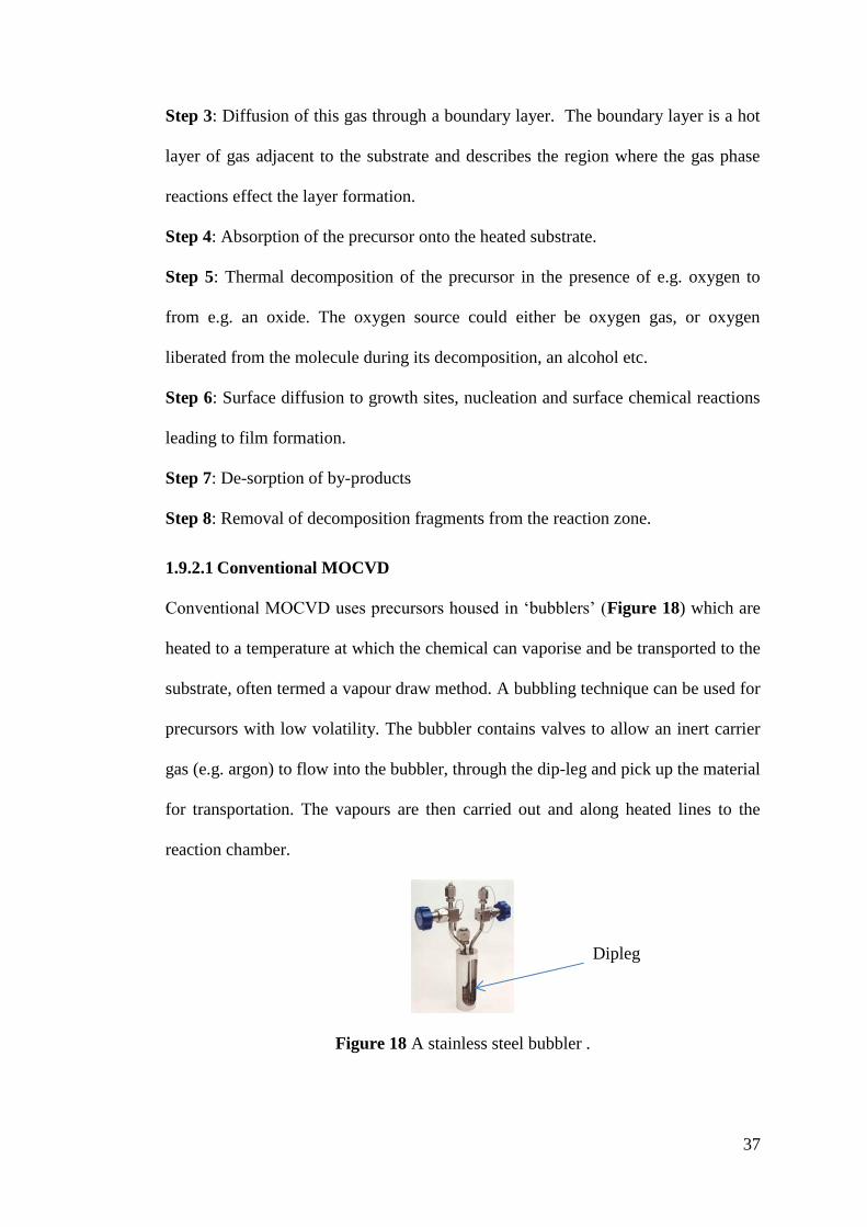
37
Step 3: Diffusion of this gas through a boundary layer. The boundary layer is a hot
layer of gas adjacent to the substrate and describes the region where the gas phase
reactions effect the layer formation.
Step 4: Absorption of the precursor onto the heated substrate.
Step 5: Thermal decomposition of the precursor in the presence of e.g. oxygen to
from e.g. an oxide. The oxygen source could either be oxygen gas, or oxygen
liberated from the molecule during its decomposition, an alcohol etc.
Step 6: Surface diffusion to growth sites, nucleation and surface chemical reactions
leading to film formation.
Step 7: De-sorption of by-products
Step 8: Removal of decomposition fragments from the reaction zone.
1.9.2.1 Conventional MOCVD
Conventional MOCVD uses precursors housed in ‘bubblers’ (Figure 18) which are
heated to a temperature at which the chemical can vaporise and be transported to the
substrate, often termed a vapour draw method. A bubbling technique can be used for
precursors with low volatility. The bubbler contains valves to allow an inert carrier
gas (e.g. argon) to flow into the bubbler, through the dip-leg and pick up the material
for transportation. The vapours are then carried out and along heated lines to the
reaction chamber.
Figure 18 A stainless steel bubbler .
Dipleg
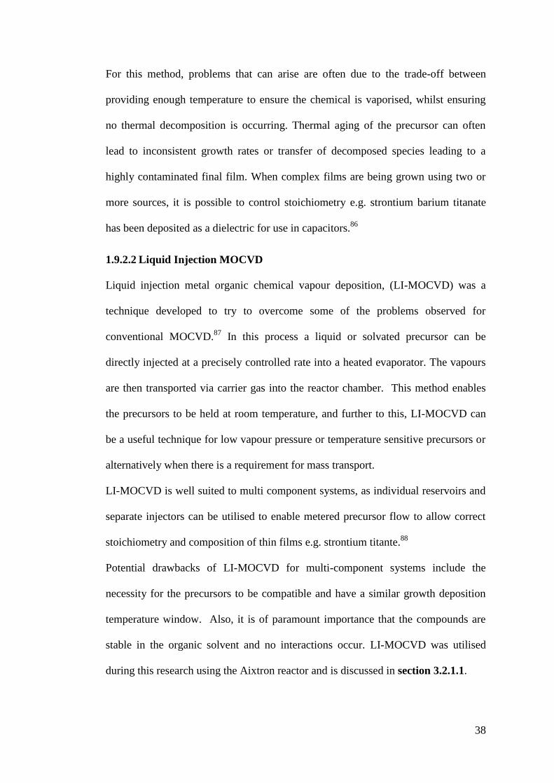
38
For this method, problems that can arise are often due to the trade-off between
providing enough temperature to ensure the chemical is vaporised, whilst ensuring
no thermal decomposition is occurring. Thermal aging of the precursor can often
lead to inconsistent growth rates or transfer of decomposed species leading to a
highly contaminated final film. When complex films are being grown using two or
more sources, it is possible to control stoichiometry e.g. strontium barium titanate
has been deposited as a dielectric for use in capacitors.86
1.9.2.2 Liquid Injection MOCVD
Liquid injection metal organic chemical vapour deposition, (LI-MOCVD) was a
technique developed to try to overcome some of the problems observed for
conventional MOCVD.87
In this process a liquid or solvated precursor can be
directly injected at a precisely controlled rate into a heated evaporator. The vapours
are then transported via carrier gas into the reactor chamber. This method enables
the precursors to be held at room temperature, and further to this, LI-MOCVD can
be a useful technique for low vapour pressure or temperature sensitive precursors or
alternatively when there is a requirement for mass transport.
LI-MOCVD is well suited to multi component systems, as individual reservoirs and
separate injectors can be utilised to enable metered precursor flow to allow correct
stoichiometry and composition of thin films e.g. strontium titante.88
Potential drawbacks of LI-MOCVD for multi-component systems include the
necessity for the precursors to be compatible and have a similar growth deposition
temperature window. Also, it is of paramount importance that the compounds are
stable in the organic solvent and no interactions occur. LI-MOCVD was utilised
during this research using the Aixtron reactor and is discussed in section 3.2.1.1.
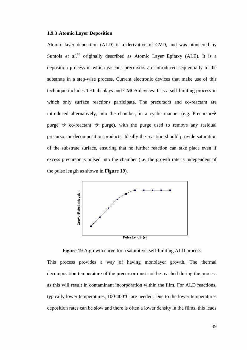
39
1.9.3 Atomic Layer Deposition
Atomic layer deposition (ALD) is a derivative of CVD, and was pioneered by
Suntola et al.89
originally described as Atomic Layer Epitaxy (ALE). It is a
deposition process in which gaseous precursors are introduced sequentially to the
substrate in a step-wise process. Current electronic devices that make use of this
technique includes TFT displays and CMOS devices. It is a self-limiting process in
which only surface reactions participate. The precursors and co-reactant are
introduced alternatively, into the chamber, in a cyclic manner (e.g. Precursor
purge co-reactant purge), with the purge used to remove any residual
precursor or decomposition products. Ideally the reaction should provide saturation
of the substrate surface, ensuring that no further reaction can take place even if
excess precursor is pulsed into the chamber (i.e. the growth rate is independent of
the pulse length as shown in Figure 19).
Figure 19 A growth curve for a saturative, self-limiting ALD process
This process provides a way of having monolayer growth. The thermal
decomposition temperature of the precursor must not be reached during the process
as this will result in contaminant incorporation within the film. For ALD reactions,
typically lower temperatures, 100-400°C are needed. Due to the lower temperatures
deposition rates can be slow and there is often a lower density in the films, this leads
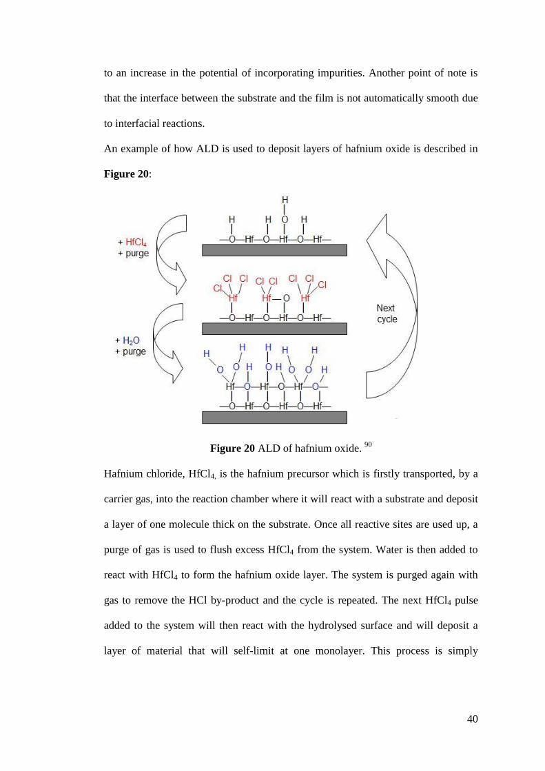
40
to an increase in the potential of incorporating impurities. Another point of note is
that the interface between the substrate and the film is not automatically smooth due
to interfacial reactions.
An example of how ALD is used to deposit layers of hafnium oxide is described in
Figure 20:
Figure 20 ALD of hafnium oxide. 90
Hafnium chloride, HfCl4, is the hafnium precursor which is firstly transported, by a
carrier gas, into the reaction chamber where it will react with a substrate and deposit
a layer of one molecule thick on the substrate. Once all reactive sites are used up, a
purge of gas is used to flush excess HfCl4 from the system. Water is then added to
react with HfCl4 to form the hafnium oxide layer. The system is purged again with
gas to remove the HCl by-product and the cycle is repeated. The next HfCl4 pulse
added to the system will then react with the hydrolysed surface and will deposit a
layer of material that will self-limit at one monolayer. This process is simply
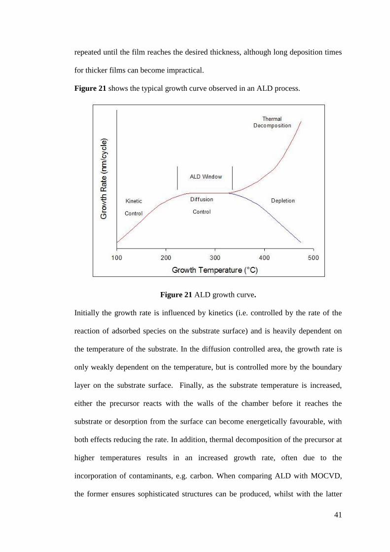
41
repeated until the film reaches the desired thickness, although long deposition times
for thicker films can become impractical.
Figure 21 shows the typical growth curve observed in an ALD process.
Figure 21 ALD growth curve.
Initially the growth rate is influenced by kinetics (i.e. controlled by the rate of the
reaction of adsorbed species on the substrate surface) and is heavily dependent on
the temperature of the substrate. In the diffusion controlled area, the growth rate is
only weakly dependent on the temperature, but is controlled more by the boundary
layer on the substrate surface. Finally, as the substrate temperature is increased,
either the precursor reacts with the walls of the chamber before it reaches the
substrate or desorption from the surface can become energetically favourable, with
both effects reducing the rate. In addition, thermal decomposition of the precursor at
higher temperatures results in an increased growth rate, often due to the
incorporation of contaminants, e.g. carbon. When comparing ALD with MOCVD,
the former ensures sophisticated structures can be produced, whilst with the latter
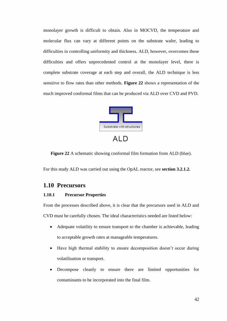
42
monolayer growth is difficult to obtain. Also in MOCVD, the temperature and
molecular flux can vary at different points on the substrate wafer, leading to
difficulties in controlling uniformity and thickness. ALD, however, overcomes these
difficulties and offers unprecedented control at the monolayer level, there is
complete substrate coverage at each step and overall, the ALD technique is less
sensitive to flow rates than other methods. Figure 22 shows a representation of the
much improved conformal films that can be produced via ALD over CVD and PVD.
Figure 22 A schematic showing conformal film formation from ALD (blue).
For this study ALD was carried out using the OpAL reactor, see section 3.2.1.2.
1.10 Precursors
1.10.1 Precursor Properties
From the processes described above, it is clear that the precursors used in ALD and
CVD must be carefully chosen. The ideal characteristics needed are listed below:
Adequate volatility to ensure transport to the chamber is achievable, leading
to acceptable growth rates at manageable temperatures.
Have high thermal stability to ensure decomposition doesn’t occur during
volatilisation or transport.
Decompose cleanly to ensure there are limited opportunities for
contaminants to be incorporated into the final film.
43
Give stable, non-toxic by-products which can be easily removed from the
reaction chamber
Have high chemical purity or be easily purified.
Be readily and commercially available at low cost
Be non-toxic, non-pyrophoric
Long-shelf life (preferably not air and moisture sensitive)
Good compatibility with co-precursors
It is difficult for all the above criteria to be fulfilled at once. As an example, many
of the industrial CVD processes use simple precursors such as metal hydrides (e.g.
SiH4), metal alkyls (e.g. Me3Al) and metal halides (e.g. SnCl4). The latter usually
requires a reducing agent and often liberates corrosive by products like HCl.
Factors which must be considered when choosing a precursor for a given process
include:
the type of ligand and the way in which it is bonded to the metal as this can
help to determine the decomposition pathway of a material
the film to be grown. If a nitride material is required, the precursor would not
contain oxygen as this could potentially contaminate the layer.
the temperature of the process to ensure the precursor is reactive yet does not
decompose and generate impurities.
the substrate to be grown on, potential temperature sensitive substrates, large
area, high throughput, the requirement of a seed layer
ease of chemical synthesis, purification and scale-up
previous patents

44
Table 5 is included to highlight the vast range of chemical precursors used in
ALD and/or CVD regimes. The materials deposited with them and the potential
incorporation of these films into end applications in the electronics industry is
summarised.
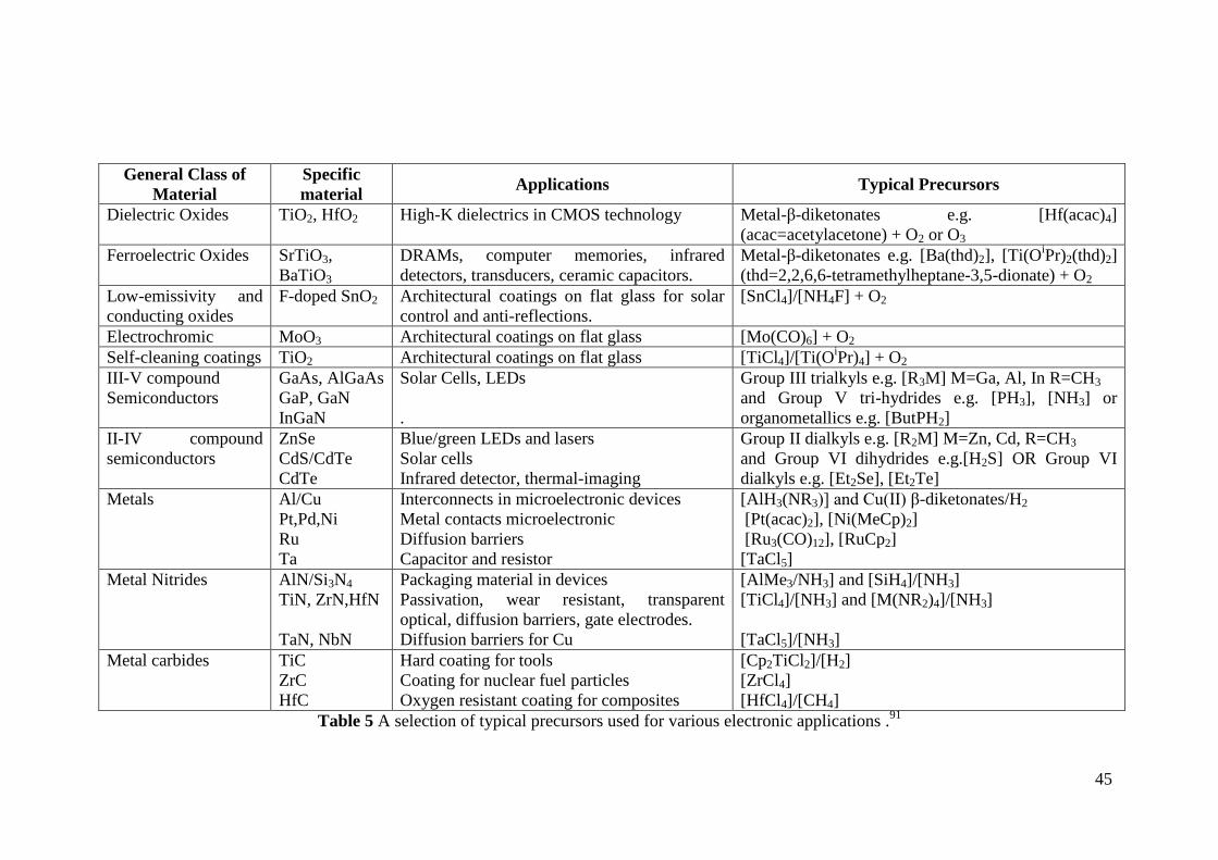
45
General Class of
Material
Specific
material Applications Typical Precursors
Dielectric Oxides TiO2, HfO2 High-K dielectrics in CMOS technology Metal-β-diketonates e.g. [Hf(acac)4]
(acac=acetylacetone) + O2 or O3
Ferroelectric Oxides SrTiO3,
BaTiO3
DRAMs, computer memories, infrared
detectors, transducers, ceramic capacitors.
Metal-β-diketonates e.g. [Ba(thd)2], [Ti(OiPr)2(thd)2]
(thd=2,2,6,6-tetramethylheptane-3,5-dionate) + O2
Low-emissivity and
conducting oxides
F-doped SnO2 Architectural coatings on flat glass for solar
control and anti-reflections.
[SnCl4]/[NH4F] + O2
Electrochromic MoO3 Architectural coatings on flat glass [Mo(CO)6] + O2
Self-cleaning coatings TiO2 Architectural coatings on flat glass [TiCl4]/[Ti(OiPr)4] + O2
III-V compound
Semiconductors
GaAs, AlGaAs
GaP, GaN
InGaN
Solar Cells, LEDs
.
Group III trialkyls e.g. [R3M] M=Ga, Al, In R=CH3
and Group V tri-hydrides e.g. [PH3], [NH3] or
organometallics e.g. [ButPH2]
II-IV compound
semiconductors
ZnSe
CdS/CdTe
CdTe
Blue/green LEDs and lasers
Solar cells
Infrared detector, thermal-imaging
Group II dialkyls e.g. [R2M] M=Zn, Cd, R=CH3
and Group VI dihydrides e.g.[H2S] OR Group VI
dialkyls e.g. [Et2Se], [Et2Te]
Metals Al/Cu
Pt,Pd,Ni
Ru
Ta
Interconnects in microelectronic devices
Metal contacts microelectronic
Diffusion barriers
Capacitor and resistor
[AlH3(NR3)] and Cu(II) β-diketonates/H2
[Pt(acac)2], [Ni(MeCp)2]
[Ru3(CO)12], [RuCp2]
[TaCl5]
Metal Nitrides AlN/Si3N4
TiN, ZrN,HfN
TaN, NbN
Packaging material in devices
Passivation, wear resistant, transparent
optical, diffusion barriers, gate electrodes.
Diffusion barriers for Cu
[AlMe3/NH3] and [SiH4]/[NH3]
[TiCl4]/[NH3] and [M(NR2)4]/[NH3]
[TaCl5]/[NH3]
Metal carbides TiC
ZrC
HfC
Hard coating for tools
Coating for nuclear fuel particles
Oxygen resistant coating for composites
[Cp2TiCl2]/[H2]
[ZrCl4]
[HfCl4]/[CH4]
Table 5 A selection of typical precursors used for various electronic applications .91
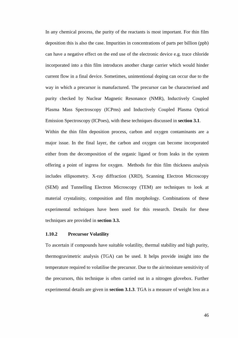
46
In any chemical process, the purity of the reactants is most important. For thin film
deposition this is also the case. Impurities in concentrations of parts per billion (ppb)
can have a negative effect on the end use of the electronic device e.g. trace chloride
incorporated into a thin film introduces another charge carrier which would hinder
current flow in a final device. Sometimes, unintentional doping can occur due to the
way in which a precursor is manufactured. The precursor can be characterised and
purity checked by Nuclear Magnetic Resonance (NMR), Inductively Coupled
Plasma Mass Spectroscopy (ICPms) and Inductively Coupled Plasma Optical
Emission Spectroscopy (ICPoes), with these techniques discussed in section 3.1.
Within the thin film deposition process, carbon and oxygen contaminants are a
major issue. In the final layer, the carbon and oxygen can become incorporated
either from the decomposition of the organic ligand or from leaks in the system
offering a point of ingress for oxygen. Methods for thin film thickness analysis
includes ellipsometry. X-ray diffraction (XRD), Scanning Electron Microscopy
(SEM) and Tunnelling Electron Microscopy (TEM) are techniques to look at
material crystalinity, composition and film morphology. Combinations of these
experimental techniques have been used for this research. Details for these
techniques are provided in section 3.3.
1.10.2 Precursor Volatility
To ascertain if compounds have suitable volatility, thermal stability and high purity,
thermogravimetric analysis (TGA) can be used. It helps provide insight into the
temperature required to volatilise the precursor. Due to the air/moisture sensitivity of
the precursors, this technique is often carried out in a nitrogen glovebox. Further
experimental details are given in section 3.1.3. TGA is a measure of weight loss as a
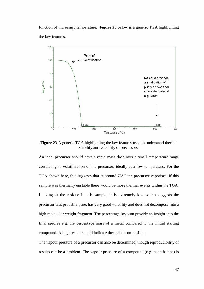
47
function of increasing temperature. Figure 23 below is a generic TGA highlighting
the key features.
Figure 23 A generic TGA highlighting the key features used to understand thermal
stability and volatility of precursors.
An ideal precursor should have a rapid mass drop over a small temperature range
correlating to volatilization of the precursor, ideally at a low temperature. For the
TGA shown here, this suggests that at around 75°C the precursor vaporises. If this
sample was thermally unstable there would be more thermal events within the TGA.
Looking at the residue in this sample, it is extremely low which suggests the
precursor was probably pure, has very good volatility and does not decompose into a
high molecular weight fragment. The percentage loss can provide an insight into the
final species e.g. the percentage mass of a metal compared to the initial starting
compound. A high residue could indicate thermal decomposition.
The vapour pressure of a precursor can also be determined, though reproducibility of
results can be a problem. The vapour pressure of a compound (e.g. naphthalene) is
48
measured at various temperatures to obtain a plot shown in Figure 24, the
experimental details are given in section 3.1.4.
Figure 24 Vapour pressure plot for naphthalene.
Through manipulation of the graph, the calculation of vapour pressure for
naphthalene at any specific temperature can be obtained from:
Equation 21: 847.12)(
7.3272)(10
KTmTorrPLog
The vapour pressure of the material provides an insight in the bubbler temperatures
needed to allow transport of the precursors. High thermal stability is required for
CVD precursors, to ensure the molecules don’t decompose during evaporation or
transport, for ALD, as it’s a self-limiting process, thermal stability is a requirement
to avoid unnecessary impurities.92
49
1.11 Summary
A literature review in Chapter 2 will introduce copper and zinc chemistry and film
deposition of zinc oxide, copper, and copper oxide. The remainder of the thesis is
organised as follows; Chapter 3 discusses the experimental methods used for both
chemical and thin film characterisation. Moving on to Chapter 4 and 5, details of
the results obtained from the synthesis and characterisation of novel precursors, in
addition to the deposition methods employed and film characterisation are
discussed. MOCVD was the deposition method of choice for the growth of n-type
Zinc Oxide nanowires, whilst ALD of p-type Copper Oxide was trialled with a view
to try to conformally coat the nanowires. A final discussion on film compositional
analysis as well as a study of the morphology and electronic properties is included.
Chapter 6 draws conclusions from the study and indicates direction for future work.
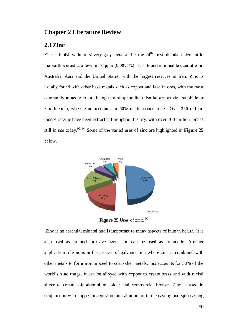
50
Chapter 2 Literature Review
2.1 Zinc
Zinc is bluish-white to silvery grey metal and is the 24th
most abundant element in
the Earth’s crust at a level of 75ppm (0.0075%). It is found in minable quantities in
Australia, Asia and the United States, with the largest reserves in Iran. Zinc is
usually found with other base metals such as copper and lead in ores, with the most
commonly mined zinc ore being that of spharelite (also known as zinc sulphide or
zinc blende), where zinc accounts for 60% of the concentrate. Over 350 million
tonnes of zinc have been extracted throughout history, with over 100 million tonnes
still in use today.93, 94
Some of the varied uses of zinc are highlighted in Figure 25
below.
Figure 25 Uses of zinc. 93
Zinc is an essential mineral and is important to many aspects of human health. It is
also used as an anti-corrosive agent and can be used as an anode. Another
application of zinc is in the process of galvanization where zinc is combined with
other metals to form iron or steel to coat other metals, this accounts for 50% of the
world’s zinc usage. It can be alloyed with copper to create brass and with nickel
silver to create soft aluminium solder and commercial bronze. Zinc is used in
conjunction with copper, magnesium and aluminium in die casting and spin casting
51
methods which are used in the automotive, electrical, and hardware industries. Zinc
has many applications in the chemical industry. In synthetic chemistry, zinc-based
compounds, when combined with transition metal reagents such as nickel or
palladium, are used for cross-coupling reactions, copper mediated substitution and
addition reactions, and catalytic asymmetric addition to aldehydes.95
2.1.1 Zinc Chemistry
Zinc is found in group 12 in the periodic table and has an electronic configuration of
[Ar] 3d10
, 4s2. The maximum oxidation state for zinc is (II); this can be reasoned by
analysing the ionization potentials. The first and second potentials, (corresponding
to the 4s electrons) are 9.39eV and 17.89eV respectively, whilst the third ionisation
potential, (corresponding to the removal one of the d-electrons from the filled shell)
is 40.0eV. As the d-level is full, the lack of participation of the d-electrons with
bonding prevents complexes with ligands including carbon monoxide, as there are
no electrons on the metal available for back donation, but complexes with ligands
such as NH3, H2O and halide ions are readily formed.
2.1.1.1 Dialkylzinc Chemistry
Organozinc chemistry originated in the synthesis of dimethyl- and diethyl- zinc by
Frankland in 1849, which were the first organometallic compounds having a metal-
carbon σ-bond.96
The discovery was accidental as Frankland was interested in the
isolation of the ethyl ‘radical’ by the action of a metal on methyl/ethyl iodide and
hydrolysis experiments of the distilled material helped to identify the compounds.97
There have been many subsequent attempts to identify and understand the structure
and bonding of these compounds.98-101
The research within this body of work has led
to the first crystal structure determination of both diethyl and dimethyl zinc102
and is
discussed in Chapter 4.
52
The route most commonly used to synthesise dialkylzinc compounds is the reaction
between anhydrous zinc chloride solvated in ether, with Grignard or lithium
reagents.
222 22 MgXZnRRMgXZnCl
Where R=Me, Et etc. and X=Cl, Br, F
After the solvent is removed under vacuum, the dialkyls can be distilled. 103
The
potential drawback of this reaction for use of the product within the electronics
industry is halide trace impurities (e.g. RZnX, RX) which can act as n-type dopants
during the growth of II-IV alloys. If, however, the dialkylzinc compound is to be
used as a p-type dopant during the growth of III-V layers the potential problem
could be the incorporation of oxygen based contaminants arising for solvents used
during synthesis.
There are two further ways in which organozincs can be formed:
1. by the direct reaction of activated zinc metal (usually by zinc-copper or zinc-
silver couple) with the required alkyl bromide or iodide, an equilibrium is
established in which the diorganozinc is formed:
)()( 1 CuZnRZnXCuZnRX nn
RZnX2 22 ZnXZnR
Where R=Me, Et etc. and X=Cl, Br, F
2. or a method rarely used now, due to the high toxicity of mercury, is a
transmetalisation reaction with zinc metal and the bisalkyl mercury
compounds.
HgZnRZnHgR 22
Where R=Me, Et etc.
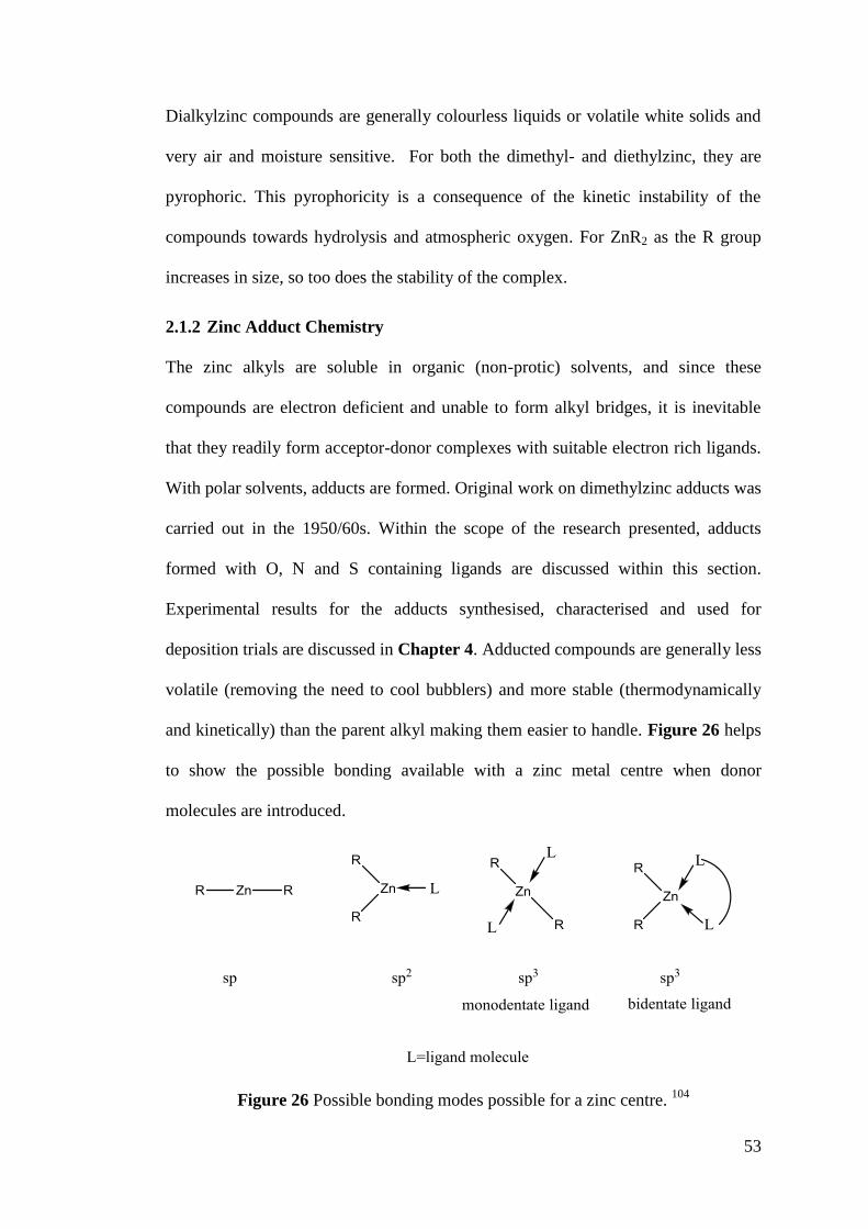
53
Dialkylzinc compounds are generally colourless liquids or volatile white solids and
very air and moisture sensitive. For both the dimethyl- and diethylzinc, they are
pyrophoric. This pyrophoricity is a consequence of the kinetic instability of the
compounds towards hydrolysis and atmospheric oxygen. For ZnR2 as the R group
increases in size, so too does the stability of the complex.
2.1.2 Zinc Adduct Chemistry
The zinc alkyls are soluble in organic (non-protic) solvents, and since these
compounds are electron deficient and unable to form alkyl bridges, it is inevitable
that they readily form acceptor-donor complexes with suitable electron rich ligands.
With polar solvents, adducts are formed. Original work on dimethylzinc adducts was
carried out in the 1950/60s. Within the scope of the research presented, adducts
formed with O, N and S containing ligands are discussed within this section.
Experimental results for the adducts synthesised, characterised and used for
deposition trials are discussed in Chapter 4. Adducted compounds are generally less
volatile (removing the need to cool bubblers) and more stable (thermodynamically
and kinetically) than the parent alkyl making them easier to handle. Figure 26 helps
to show the possible bonding available with a zinc metal centre when donor
molecules are introduced.
Figure 26 Possible bonding modes possible for a zinc centre. 104
54
Throughout this study the adducted compounds will carry the notation DMZn.L
where L is the ligand used.
2.1.2.1 Oxygen Donor Adducts
Oxygen donor complexes formed with dialkyl zinc increase in stability from simple
ethers<cyclic ethers<chelating ethers. The Zn atom bonds with the oxygen on the
donor ligand. An example of a complex with a simple ether is Me2Zn.O(CH3)2
formed with dimethyl ether, (CH3OCH3). This adducted species has a boiling point
of 47°C, just 3°C higher than that of dimethyl zinc. With simple ethers, the
purification distillation process can cause partial separation even at atmospheric
pressure. Cyclic ethers e.g. tetrahydrofuran, THF, (O(CH2)4) and 1,4-dioxane
(O(C2H4)2O) are more stable due to the increased steric bulk. These compounds are
miscible in water as the oxygen atom is more available for hydrogen bonding when
compared to aliphatic ethers. The DMZn.L adducted species using both THF and
1,4-dioxane cyclic ligands, were target molecules and are discussed in-depth in
Chapter 4. Chelating ethers are most stable and often incorporate multi-dentate
ligands. Previously, the DMZn.L where L=1,2-dimethoxyethane was reported as a
non-chelating compound105
, this study concludes that this complex is monomeric
featuring a chelating 1,2-dimethoxyethane ligand.106
2.1.2.2 Nitrogen Donor Adducts
Research on reactions between zinc alkyls and amines has been extensive. Table 6
has been compiled from the literature and includes some of the DMZn.L compounds
(where L=a nitrogen containing ligand) reported. The ligands are indicated along
with melting point and boiling points of the final compounds with DMZn included
for reference.
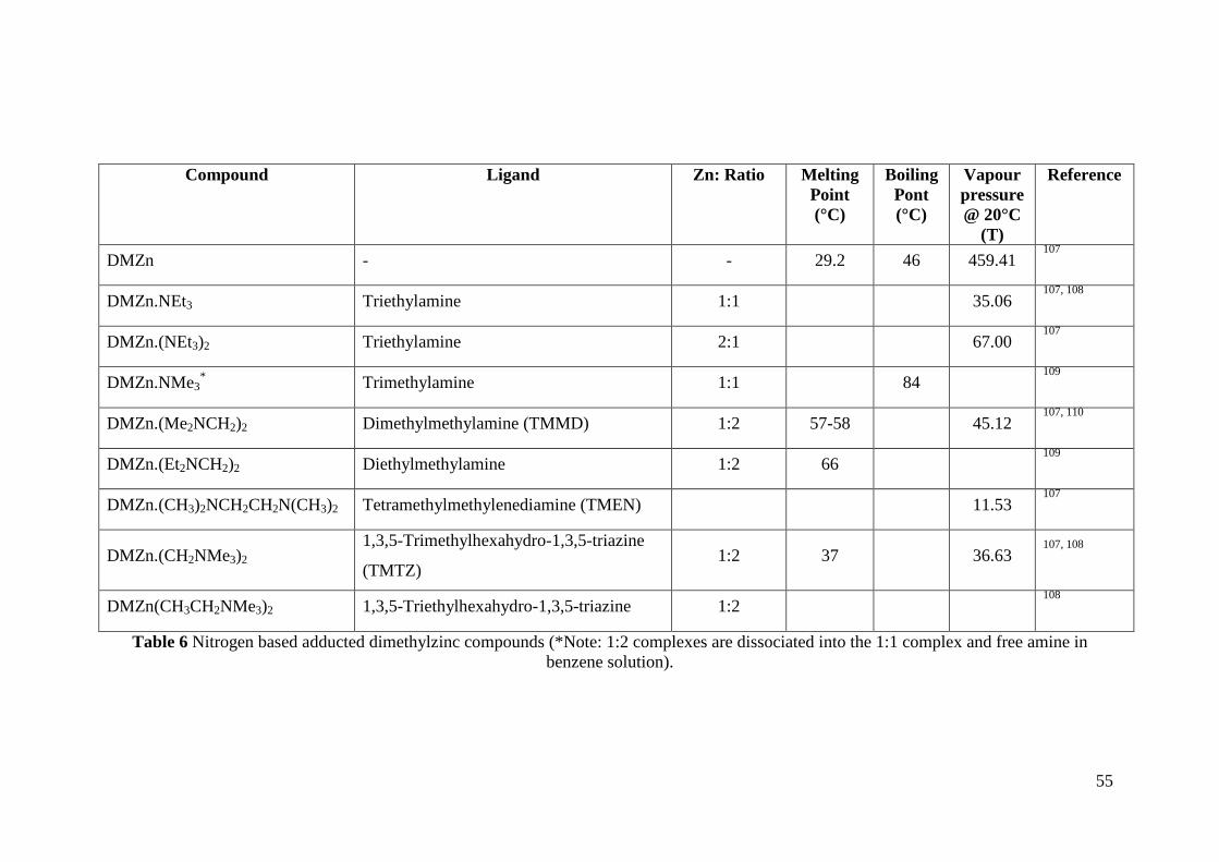
55
Compound Ligand Zn: Ratio Melting
Point
(°C)
Boiling
Pont
(°C)
Vapour
pressure
@ 20°C
(T)
Reference
DMZn - - 29.2 46 459.41 107
DMZn.NEt3 Triethylamine 1:1 35.06 107, 108
DMZn.(NEt3)2 Triethylamine 2:1 67.00 107
DMZn.NMe3* Trimethylamine 1:1 84
109
DMZn.(Me2NCH2)2 Dimethylmethylamine (TMMD) 1:2 57-58 45.12 107, 110
DMZn.(Et2NCH2)2 Diethylmethylamine 1:2 66 109
DMZn.(CH3)2NCH2CH2N(CH3)2 Tetramethylmethylenediamine (TMEN) 11.53 107
DMZn.(CH2NMe3)2 1,3,5-Trimethylhexahydro-1,3,5-triazine
(TMTZ) 1:2 37 36.63
107, 108
DMZn(CH3CH2NMe3)2 1,3,5-Triethylhexahydro-1,3,5-triazine 1:2 108
Table 6 Nitrogen based adducted dimethylzinc compounds (*Note: 1:2 complexes are dissociated into the 1:1 complex and free amine in
benzene solution).
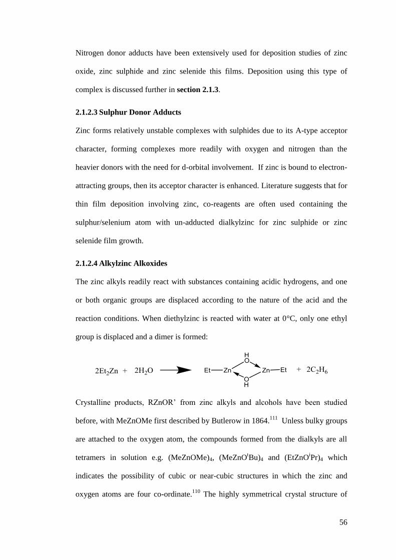
56
Nitrogen donor adducts have been extensively used for deposition studies of zinc
oxide, zinc sulphide and zinc selenide this films. Deposition using this type of
complex is discussed further in section 2.1.3.
2.1.2.3 Sulphur Donor Adducts
Zinc forms relatively unstable complexes with sulphides due to its A-type acceptor
character, forming complexes more readily with oxygen and nitrogen than the
heavier donors with the need for d-orbital involvement. If zinc is bound to electron-
attracting groups, then its acceptor character is enhanced. Literature suggests that for
thin film deposition involving zinc, co-reagents are often used containing the
sulphur/selenium atom with un-adducted dialkylzinc for zinc sulphide or zinc
selenide film growth.
2.1.2.4 Alkylzinc Alkoxides
The zinc alkyls readily react with substances containing acidic hydrogens, and one
or both organic groups are displaced according to the nature of the acid and the
reaction conditions. When diethylzinc is reacted with water at 0°C, only one ethyl
group is displaced and a dimer is formed:
Crystalline products, RZnOR’ from zinc alkyls and alcohols have been studied
before, with MeZnOMe first described by Butlerow in 1864.111
Unless bulky groups
are attached to the oxygen atom, the compounds formed from the dialkyls are all
tetramers in solution e.g. (MeZnOMe)4, (MeZnOtBu)4 and (EtZnO
iPr)4 which
indicates the possibility of cubic or near-cubic structures in which the zinc and
oxygen atoms are four co-ordinate.110
The highly symmetrical crystal structure of
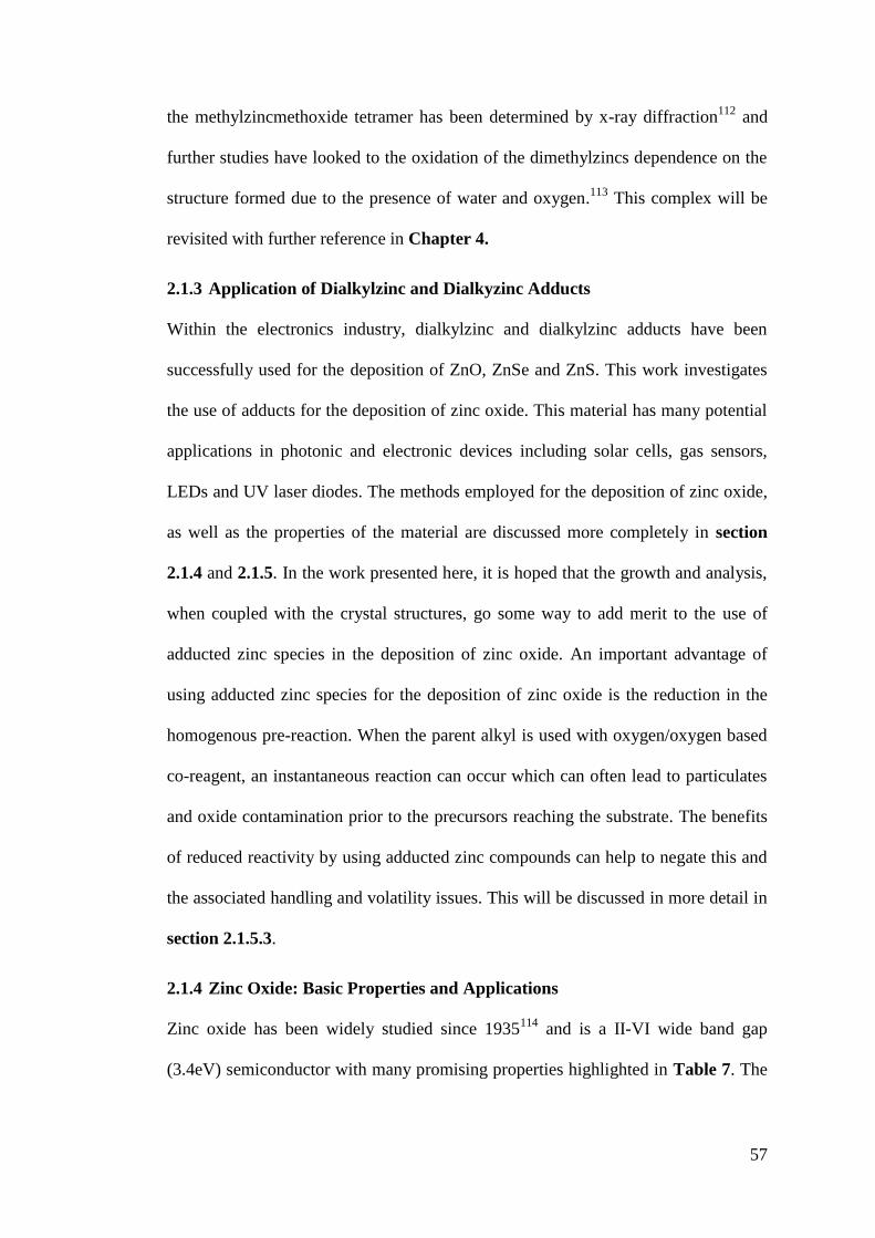
57
the methylzincmethoxide tetramer has been determined by x-ray diffraction112
and
further studies have looked to the oxidation of the dimethylzincs dependence on the
structure formed due to the presence of water and oxygen.113
This complex will be
revisited with further reference in Chapter 4.
2.1.3 Application of Dialkylzinc and Dialkyzinc Adducts
Within the electronics industry, dialkylzinc and dialkylzinc adducts have been
successfully used for the deposition of ZnO, ZnSe and ZnS. This work investigates
the use of adducts for the deposition of zinc oxide. This material has many potential
applications in photonic and electronic devices including solar cells, gas sensors,
LEDs and UV laser diodes. The methods employed for the deposition of zinc oxide,
as well as the properties of the material are discussed more completely in section
2.1.4 and 2.1.5. In the work presented here, it is hoped that the growth and analysis,
when coupled with the crystal structures, go some way to add merit to the use of
adducted zinc species in the deposition of zinc oxide. An important advantage of
using adducted zinc species for the deposition of zinc oxide is the reduction in the
homogenous pre-reaction. When the parent alkyl is used with oxygen/oxygen based
co-reagent, an instantaneous reaction can occur which can often lead to particulates
and oxide contamination prior to the precursors reaching the substrate. The benefits
of reduced reactivity by using adducted zinc compounds can help to negate this and
the associated handling and volatility issues. This will be discussed in more detail in
section 2.1.5.3.
2.1.4 Zinc Oxide: Basic Properties and Applications
Zinc oxide has been widely studied since 1935114
and is a II-VI wide band gap
(3.4eV) semiconductor with many promising properties highlighted in Table 7. The
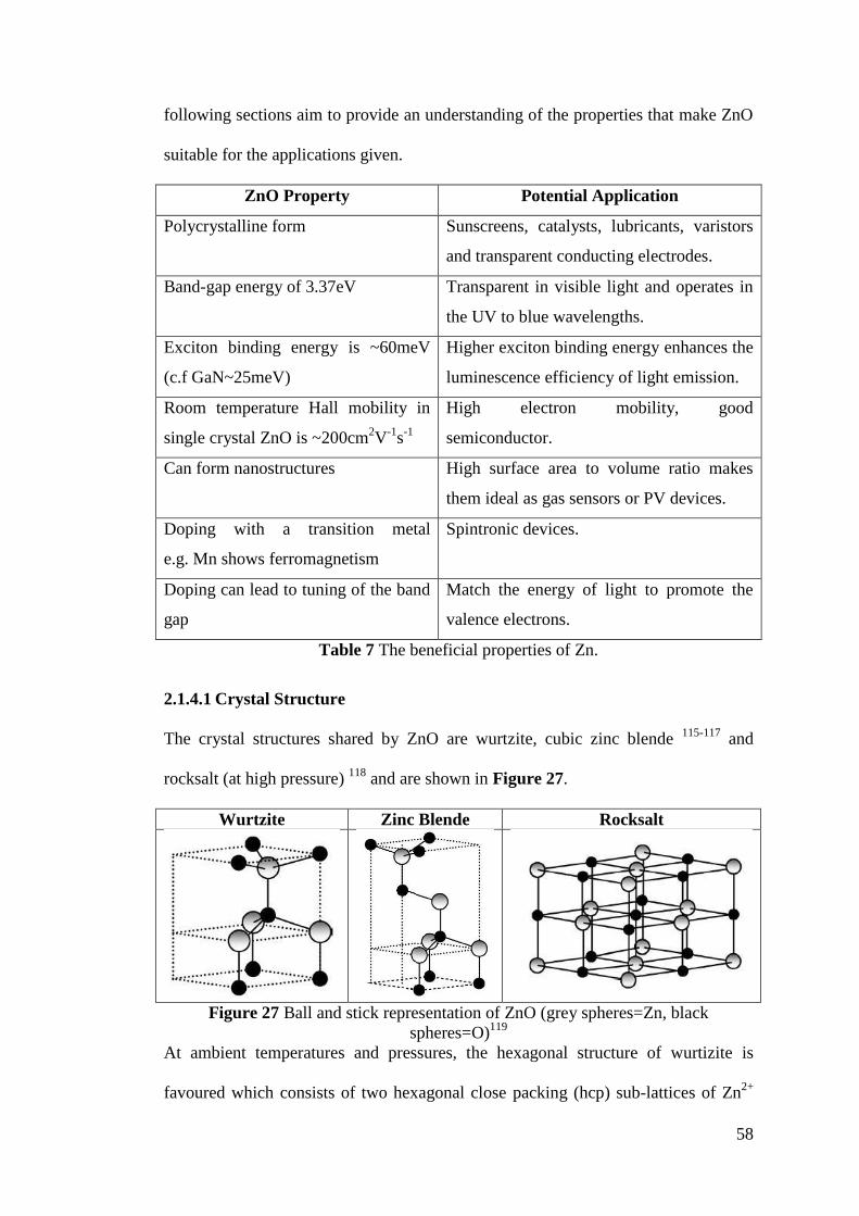
58
following sections aim to provide an understanding of the properties that make ZnO
suitable for the applications given.
ZnO Property Potential Application
Polycrystalline form Sunscreens, catalysts, lubricants, varistors
and transparent conducting electrodes.
Band-gap energy of 3.37eV Transparent in visible light and operates in
the UV to blue wavelengths.
Exciton binding energy is ~60meV
(c.f GaN~25meV)
Higher exciton binding energy enhances the
luminescence efficiency of light emission.
Room temperature Hall mobility in
single crystal ZnO is ~200cm2V
-1s
-1
High electron mobility, good
semiconductor.
Can form nanostructures High surface area to volume ratio makes
them ideal as gas sensors or PV devices.
Doping with a transition metal
e.g. Mn shows ferromagnetism
Spintronic devices.
Doping can lead to tuning of the band
gap
Match the energy of light to promote the
valence electrons.
Table 7 The beneficial properties of Zn.
2.1.4.1 Crystal Structure
The crystal structures shared by ZnO are wurtzite, cubic zinc blende 115-117
and
rocksalt (at high pressure) 118
and are shown in Figure 27.
Wurtzite Zinc Blende Rocksalt
Figure 27 Ball and stick representation of ZnO (grey spheres=Zn, black
spheres=O)119
At ambient temperatures and pressures, the hexagonal structure of wurtizite is
favoured which consists of two hexagonal close packing (hcp) sub-lattices of Zn2+
59
and O2-
. Each Zn ion is surrounded by a tetrahedron of O ions and vice versa. The
tetrahedral co-ordination leads to polar symmetry along the hexagonal axis. This
polarity is responsible for the piezoelectric properties, and is a key factor in crystal
growth and defect generation in ZnO.120
The tetrahedral co-ordination is an
indicator of sp3 covalent bonding, however, the Zn-O bond possesses a very strong
ionic character, and thus, ZnO lies on the border of being classed as ionic or
covalent.121
The lattice parameters of the hexagonal unit cell are a=3.2495Å and
c=5.2069Å with a density of 5.605gcm-3
.122
At high pressures in the region of 10GPa
there is a reduction of the lattice dimensions, causing the Coulomb interaction to
favour the ionic over the covalent structure and the rocksalt structure is formed, but
is difficult to stabilize.118
The zinc-blende structure is only stabilized by growth on
cubic substrates such as GaAs, SiO2, and Si indicating the need for lattice matching
to overcome the tendency to form the wurtzitic phase. A more comprehensive
discussion of the crystal structures, with supporting references, is given by Özgür et
al. in a review article entitled ‘A comprehensive review of ZnO materials and
devices’.123
2.1.4.2 Band Structure
Understanding the band structure of a semiconductor is essential for determining its
potential use and incorporation into a device. Numerous theoretical and
experimental studies have been employed to try to establish the band structure of the
electronic states of wurtzitic ZnO. Absorption or emission techniques using X-rays
or UV have been used to measure the energy difference by inducing transitions
between electronic levels. Photoelectron spectroscopy is based upon the
photoelectric effect, whereby the peaks in the emission spectra correspond to
electron emission from a core level without inelastic scattering. Angle-resolved
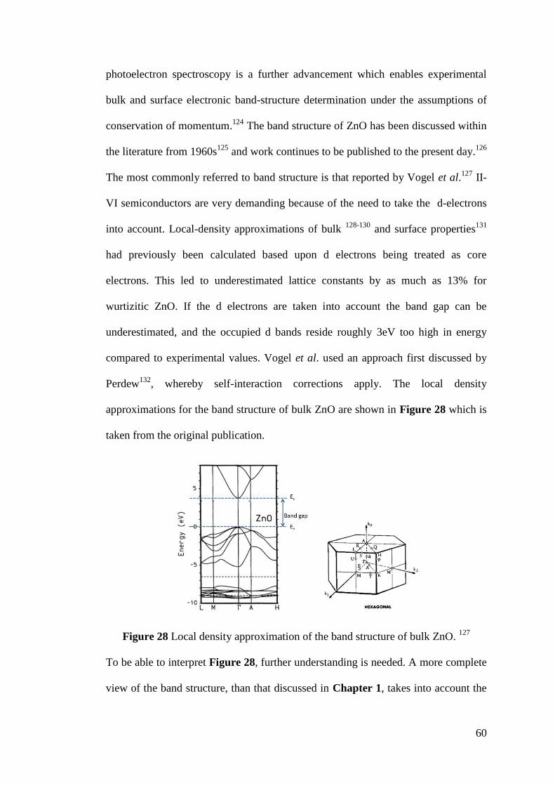
60
photoelectron spectroscopy is a further advancement which enables experimental
bulk and surface electronic band-structure determination under the assumptions of
conservation of momentum.124
The band structure of ZnO has been discussed within
the literature from 1960s125
and work continues to be published to the present day.126
The most commonly referred to band structure is that reported by Vogel et al.127
II-
VI semiconductors are very demanding because of the need to take the d-electrons
into account. Local-density approximations of bulk 128-130
and surface properties131
had previously been calculated based upon d electrons being treated as core
electrons. This led to underestimated lattice constants by as much as 13% for
wurtizitic ZnO. If the d electrons are taken into account the band gap can be
underestimated, and the occupied d bands reside roughly 3eV too high in energy
compared to experimental values. Vogel et al. used an approach first discussed by
Perdew132
, whereby self-interaction corrections apply. The local density
approximations for the band structure of bulk ZnO are shown in Figure 28 which is
taken from the original publication.
Figure 28 Local density approximation of the band structure of bulk ZnO. 127
To be able to interpret Figure 28, further understanding is needed. A more complete
view of the band structure, than that discussed in Chapter 1, takes into account the
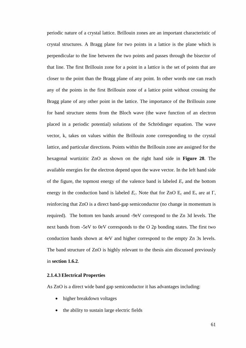
61
periodic nature of a crystal lattice. Brillouin zones are an important characteristic of
crystal structures. A Bragg plane for two points in a lattice is the plane which is
perpendicular to the line between the two points and passes through the bisector of
that line. The first Brillouin zone for a point in a lattice is the set of points that are
closer to the point than the Bragg plane of any point. In other words one can reach
any of the points in the first Brillouin zone of a lattice point without crossing the
Bragg plane of any other point in the lattice. The importance of the Brillouin zone
for band structure stems from the Bloch wave (the wave function of an electron
placed in a periodic potential) solutions of the Schrödinger equation. The wave
vector, k, takes on values within the Brillouin zone corresponding to the crystal
lattice, and particular directions. Points within the Brillouin zone are assigned for the
hexagonal wurtizitic ZnO as shown on the right hand side in Figure 28. The
available energies for the electron depend upon the wave vector. In the left hand side
of the figure, the topmost energy of the valence band is labeled Ev and the bottom
energy in the conduction band is labeled Ec. Note that for ZnO Ec and Ev are at Γ,
reinforcing that ZnO is a direct band-gap semiconductor (no change in momentum is
required). The bottom ten bands around -9eV correspond to the Zn 3d levels. The
next bands from -5eV to 0eV corresponds to the O 2p bonding states. The first two
conduction bands shown at 4eV and higher correspond to the empty Zn 3s levels.
The band structure of ZnO is highly relevant to the thesis aim discussed previously
in section 1.6.2.
2.1.4.3 Electrical Properties
As ZnO is a direct wide band gap semiconductor it has advantages including:
higher breakdown voltages
the ability to sustain large electric fields
62
high-temperature/high power operation
ZnO has been extensively studied, and due to this there is a large variance in the
quality of samples, and in turn, electrical properties reported. Looking to electron
mobility values at room temperature, the values include 120, 137 and 145cm
2V
-1s
-1.
133,134,135. Kaidashev et al.
136 report the best reproducible electron motilities from
115 to 155cm2/V at 300K for a carrier concentration range of 2x10
16 to 5x10
16cm
-3
for a 1-2µm ZnO thin film. It is worth reinforcing here, that often undoped wurtiztic
ZnO can become an n-type semiconductor due to defects such as Zn on O, Zn
interstitial and O vacancies.137-139
2.1.4.4 Thermal Properties
2.1.4.4.1 Thermal Expansion Co-efficient
The thermal expansion co-efficient of a material describes the lattice expansion as a
function of temperature. This property is dependent on stoichiometry, defects and
free carrier concentration.123
For zinc oxide these co-efficients are given as
αa=4.31x10⁻⁶K-1 (normal to the c-axis) and αc=2.49 x 10⁻⁶K-1 (parallel to the c-
axis) at 300K.140
For possible future applications of the wide-gap material ZnO in
high temperature electronics, the thermal expansion coefficients at elevated
temperatures are of relevance. Ibach141
presented data up to T =800 K that there is
an increase in the thermal expansion coefficient with temperature, with saturation
near to 800K, yielding the high-temperature values αa=4.98x10⁻⁶
K-1
and αc=8.30x10-
6K
-1 i.e. an enhancement factor of about 1.7 with respect to the 300K values.
142
2.1.4.4.2 Thermal Conductivity
The bulk thermal conductivity of ZnO, denoted κ (Wcm-1
K-1
) has yet to be
confirmed, with reported literature values ranging from 0.6 to 1.2Wcm-1
K-1
.123, 143
63
This kinetic property is important when considering high power/temperature
devices. It is influenced by the vibrational, rotational and electronic degrees of
freedom and is ultimately limited by phonon-phonon scattering in a crystal.144
ZnO
contains a large number of defects which reduces the thermal conductivity. A more
comprehensive discussion is given in the following review article by Özgür et al. 123
2.1.5 Zinc Oxide Thin Film Growth
Growth techniques to fabricate ZnO range from low cost wet chemical growth at
almost room temperature, to high purity deposition at temperatures above 1000°C.
Previously ZnO has been deposited by many different methods including:
o vapour liquid solid epitaxial growth (VLSE)
o pulsed laser deposition (PLD)
o magnetron sputtering
o molecular-beam epitaxy
o hydrothermal (low temperature-solution process)
o electrochemical
High temperature gas-phase processes often generates high quality ZnO but the
commercial potential is restricted due to cost implications of achieving this high
temperature, and the previous/subsequent thermal budget in the device structure. In
contrast, the low temperature solution routes are of lower cost, and suitable for large
scale production. In most cases, there is a strong tendency of c-axis orientated
growth, leading to higher growth rate in this direction over other crystal directions.
This often leads to columnar growth even at low temperatures. This phenomenon
can result is the formation of nanowires, (a 3D structure with diameter of the order
of a nanometer (10-9
m)) and is discussed further in section 2.1.6. The data reported
in the literature for ZnO deposition is too extensive to cover here. To remain focused
64
on the relevant prior work in the areas discussed within context for this research, this
literature review will focus on MOCVD of ZnO thin films and nanowires grown
only from simple zinc alkyls, alkylzinc alkoxides and adducted zinc alkyls.
MOCVD was the method of choice for the research presented due to its advantages
highlighted previously in Chapter 1.
2.1.5.1 ZnO Deposition using Dialkylzinc
Traditional methods for ZnO growth by MOCVD has involved the pyrolysis of
dimethylzinc145
or diethyl zinc 146-148
in the presence of oxygen and/or water. For
MOCVD surface reactions at the substrate should occur, but not in the gas phase.
The alkyl zincs are highly oxygen sensitive and often pre-reaction in the gas phase
can form oxide particulates upstream of the substrate. MOCVD methods have
looked to reactor pressure to try to control the reaction, with the range spanning 5-
250 torr,149-151
with superior crystal quality observed for ZnO grown at 6 Torr as
opposed to <1Torr.152
The effect of altering the oxygen partial pressure during
deposition on structure, optical and electrical properties has also been studied.153, 154
Another approach to try to overcome pre-reaction, was to look towards less reactive
oxidants. These include CO2155
, N2O155-157
and NO2 157-160
or alternatively alcohols
such as methanol, ethanol, isopropanol161, 162
or tertiary-butanol.163
Ogata et al. highlighted the potential use of nitrous oxide to grow highly crystalline
ZnO films with good optical properties.162
Kirchner et al. have carried out a
comparison of using alternative precursors for oxygen using DEZn with isopropanol
and tertiary butanol co-reagents on a sapphire substrate.164
There was a large
discrepancy in the growth rate with temperature dependence between the two
oxygen sources. Tertiary-butanol had a constant growth rate (2.1µm/hr) for the
temperature range 380-510°C. When isopropanol was used the maximum growth
65
rate was achieved at 380°C and at higher temperature fell rapidly. Film analysis
showed superior quality in the tertiary butanol grown samples. It has been proposed
that reaction of the alcohols with the dialkyzincs leads to alcohol adducts or zinc
alkoxides as the gas-phase intermediates. This theory is further supported by the
growth of ZnO by single-source zinc precursors e.g. [MeZn(OiPr)] and
[MeZn(OtBu)] without the need for an additional oxygen source.
165 A
decomposition pathway, reported by Auld, proposed the the removal of a β-
hydrogen results in the elimination of methane and an alkene. 165
ZnO has been successfully grown on numerous types of substrates including, but not
limited to, silicon,166
glass,167
gallium arsenide,168
diamond169
and sapphire.170
The
study presented in Chapter 4 uses silicon and glass substrates.
2.1.5.2 ZnO Deposition using Dialkylzinc Adducts
Using adducted zinc species for ZnO deposition has the advantage of a reduction in
the homogenous reaction before the precursors reach the substrate. Although
reaction design can help to limit the pre-reaction, making alterations to the Zn
species to make them less reactive towards oxygen, has resulted in a large number of
adducts being examined as potential precursors. Adducts of zinc with 1,4-
dioxane,171-173
thioxane,173
triethylamine,174-179
or triazine174
have been used as
precursor for MOCVD and can be successfully use to inhibit the pre-reaction for
chalcogenide and metal alkyls. Dimethylzinc.triethyl amine synthesis was reported
by Thiele in the 1960s, and has been used to study the p-type doping of III-V
materials with zinc180, 181
and also useful for the deposition of chalcogenides.182
Despite using such compounds during MOCVD, little is known about the gas
species present during the reaction. Infrared studies have been performed in the past
which show the adducts of dimethylzinc to be fully dissociated in the gas phase.183
66
2.1.5.3 Use of Adducts for the Prevention of Pre-reaction.
There are a number of ways in which adducts could be operating in controlling
unwanted reactions:
decreased reactivity of the adducted species compared to the parent alkyl
ensure surface catalysed reactions in the cool zone of the reactor are less
likely.
using high purity reagents leads to less unwanted side reactions. The
improved purity of the alkyls due to subsequent reactions/purifications may
prove important.
the pure alkyls are extremely volatile. With an adducted species, mass flow
can be more controlled. As the homogenous reactions are likely to proceed at
rates proportional to the partial pressure of the alkyls, a lower partial
pressure for the adducted species leads to a lower rate of homogenous
reaction.
The Lewis bases from which the adducts are formed may play a role in
trapping intermediates generated during the decomposition of alkyls.
It is important to note that the adducts do not need to stop the formation of
precipitates from the vapour phase, but only to inhibit their formation so that they
can pass trhough the hot zone of the reactor.
2.1.6 Zinc Oxide Nanowire Growth
Since the surface properties of ZnO are very different for the different crystal forms,
chemical reactivity and growth rate vary drastically as a function of surface
oreintations. In combination with a large surface diffusion of Zn, this often leads to
the formation of ZnO crystallites on the micro- or nano-scale. Under some
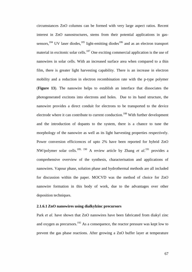
67
circumstances ZnO columns can be formed with very large aspect ratios. Recent
interest in ZnO nanostructures, stems from their potential applications in gas-
sensors,184
UV laser diodes,185
light-emitting diodes186
and as an electron transport
material in excitonic solar cells.187
One exciting commercial application is the use of
nanowires in solar cells. With an increased surface area when compared to a thin
film, there is greater light harvesting capability. There is an increase in electron
mobility and a reduction in electron recombination rate with the p-type polymer
(Figure 13). The nanowire helps to establish an interface that dissociates the
photogenerated excitons into electrons and holes. Due to its band structure, the
nanowire provides a direct conduit for electrons to be transported to the device
electrode where it can contribute to current conduction.188
With further development
and the introduction of dopants to the system, there is a chance to tune the
morphology of the nanowire as well as its light harvesting properties respectively.
Power conversion efficicences of upto 2% have been reported for hybrid ZnO
NW/polymer solar cells.189, 190
A review article by Zhang et al.191
provides a
comprehensive overview of the synthesis, characterisation and applications of
nanowires. Vapour phase, solution phase and hydrothermal methods are all included
for discussion within the paper. MOCVD was the method of choice for ZnO
nanowire formation in this body of work, due to the advantages over other
deposition techniques.
2.1.6.1 ZnO nanowires using dialkylzinc precursors
Park et al. have shown that ZnO nanowires have been fabricated from diakyl zinc
and oxygen as precursors.192
As a consequence, the reactor pressure was kept low to
prevent the gas phase reactions. After growing a ZnO buffer layer at temperature
68
below 400°C on Al2O3 substrate, nanowires were grown in the temperature range
was between 400-500°C. Figure 29 shows the SEM images of the nanowires grown.
Figure 29 SEM images of ZnO nanowires from dialkylzinc and oxygen recorded by
Park et al. 192
showing a) plan view b) tilted images(diameter 25nm) c and d) tilted
and cross-sectional view of nanowires with 70nm.
Lui et al. 193
also report ZnO nanowire growth using the same precursors. The
substrates used, c-plane sapphire, platinum on SiO2/Si and Si(100), were held at a
temperature of 700°C. An initial plasma step was performed to provide a nucleation
layer of ZnO. Saphhire and platinum surfaces gave well aligned nanowires, whilst
those on Si were randomly orientated. The dimensions of the wires were reported to
be between 20-75nm in diameter and 2µm in length.
DEZn and oxygen have also been used to deposit ZnO nanowires on αAl2O3(0001)
substrates with different ZnO buffer layers via MOCVD both in-situ and ex-situ;194
• In-situ
• ZnO buffer layer deposited on Al2O3 substrate and subsequently ZnO
nanorods grown on the buffer layer by MOCVD with substrate
temperatures of 350-650°C.
• Ex-situ
• ZnO buffer layer sputtered onto Al2O3 substrate held at 600°C. The
ZnO buffer layer/Al2O3 transferred to MOCVD chamber in air. The
ZnO nanorods were then grown on ZnO buffer layer by MOCVD.
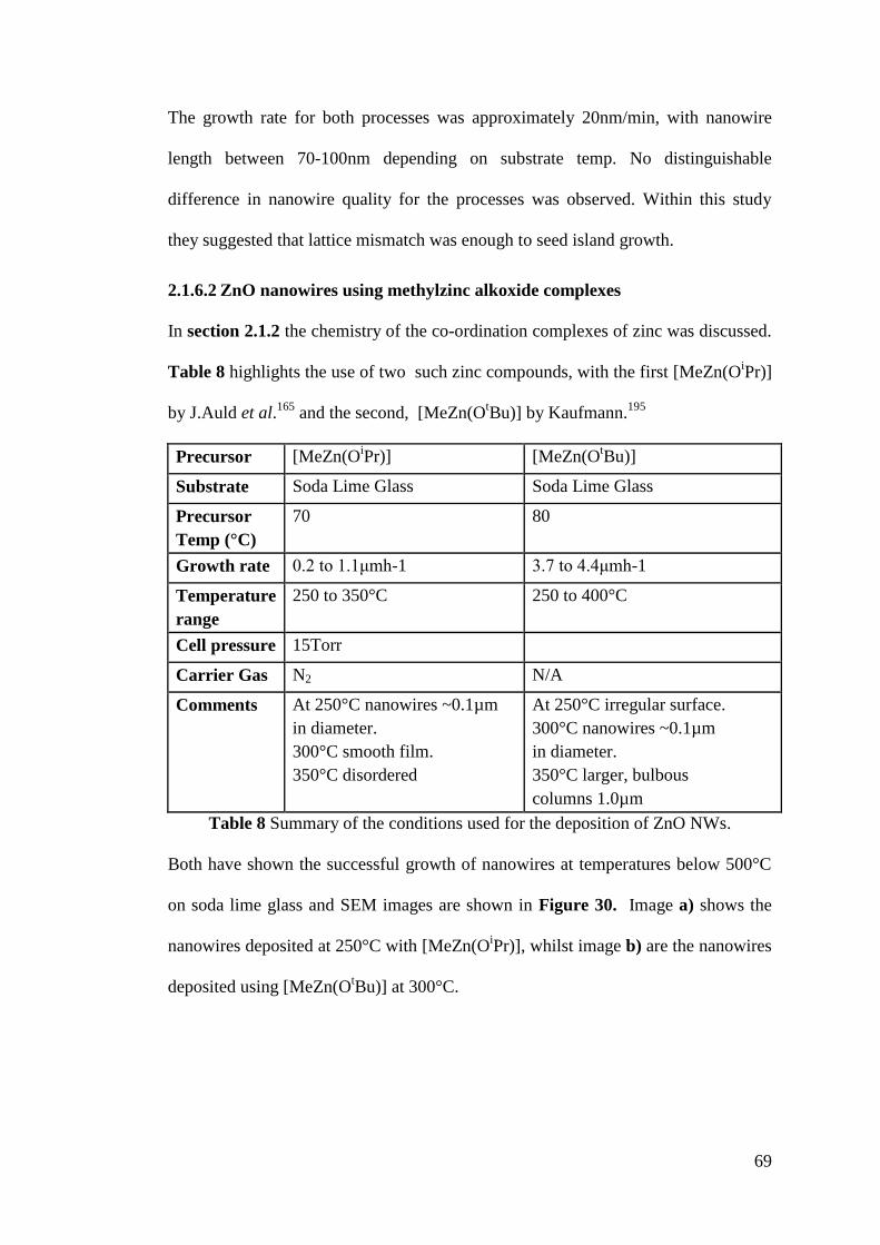
69
The growth rate for both processes was approximately 20nm/min, with nanowire
length between 70-100nm depending on substrate temp. No distinguishable
difference in nanowire quality for the processes was observed. Within this study
they suggested that lattice mismatch was enough to seed island growth.
2.1.6.2 ZnO nanowires using methylzinc alkoxide complexes
In section 2.1.2 the chemistry of the co-ordination complexes of zinc was discussed.
Table 8 highlights the use of two such zinc compounds, with the first [MeZn(OiPr)]
by J.Auld et al.165
and the second, [MeZn(OtBu)] by Kaufmann.
195
Precursor [MeZn(OiPr)] [MeZn(O
tBu)]
Substrate Soda Lime Glass Soda Lime Glass
Precursor
Temp (°C)
70 80
Growth rate 0.2 to 1.1μmh-1 3.7 to 4.4μmh-1
Temperature
range
250 to 350°C 250 to 400°C
Cell pressure 15Torr
Carrier Gas N2 N/A
Comments At 250°C nanowires ~0.1µm
in diameter.
300°C smooth film.
350°C disordered
At 250°C irregular surface.
300°C nanowires ~0.1µm
in diameter.
350°C larger, bulbous
columns 1.0µm
Table 8 Summary of the conditions used for the deposition of ZnO NWs.
Both have shown the successful growth of nanowires at temperatures below 500°C
on soda lime glass and SEM images are shown in Figure 30. Image a) shows the
nanowires deposited at 250°C with [MeZn(OiPr)], whilst image b) are the nanowires
deposited using [MeZn(OtBu)] at 300°C.
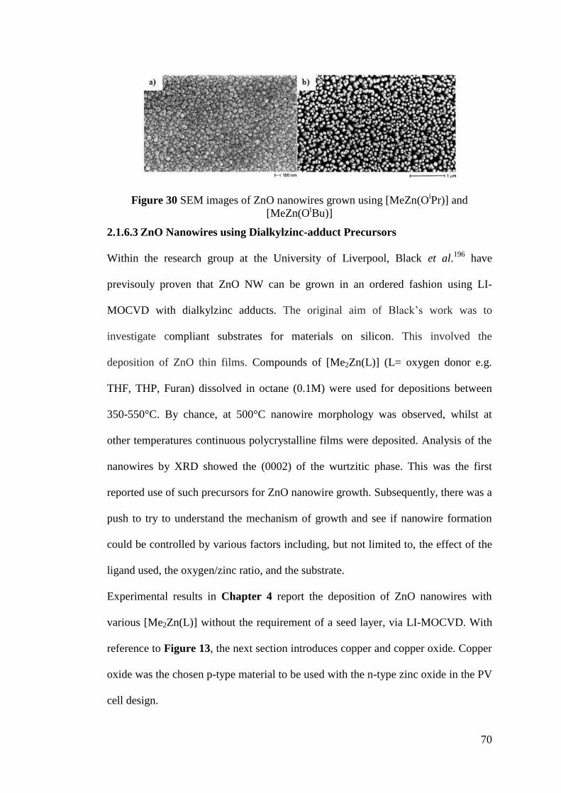
70
Figure 30 SEM images of ZnO nanowires grown using [MeZn(OiPr)] and
[MeZn(OtBu)]
2.1.6.3 ZnO Nanowires using Dialkylzinc-adduct Precursors
Within the research group at the University of Liverpool, Black et al.196
have
previsouly proven that ZnO NW can be grown in an ordered fashion using LI-
MOCVD with dialkylzinc adducts. The original aim of Black’s work was to
investigate compliant substrates for materials on silicon. This involved the
deposition of ZnO thin films. Compounds of [Me2Zn(L)] (L= oxygen donor e.g.
THF, THP, Furan) dissolved in octane (0.1M) were used for depositions between
350-550°C. By chance, at 500°C nanowire morphology was observed, whilst at
other temperatures continuous polycrystalline films were deposited. Analysis of the
nanowires by XRD showed the (0002) of the wurtzitic phase. This was the first
reported use of such precursors for ZnO nanowire growth. Subsequently, there was a
push to try to understand the mechanism of growth and see if nanowire formation
could be controlled by various factors including, but not limited to, the effect of the
ligand used, the oxygen/zinc ratio, and the substrate.
Experimental results in Chapter 4 report the deposition of ZnO nanowires with
various [Me2Zn(L)] without the requirement of a seed layer, via LI-MOCVD. With
reference to Figure 13, the next section introduces copper and copper oxide. Copper
oxide was the chosen p-type material to be used with the n-type zinc oxide in the PV
cell design.
71
2.2 Copper
Copper is an extremely ductile metal and is distinctively red in colour. It is an
excellent electrical conductor, with high thermal conductivity and is also corrosion
resistant and antibacterial. Copper can be naturally occurring but today is obtained
from minerals such as azurite (copper carbonate (Cu2(OH)2CO3)); chalcocite (copper
sulfide (Cu2S)); chalcopyrite (copper iron sulfide (CuFeS2)); and cuprite (copper
oxide (Cu2O)). Copper is mined in more than 50 nations, with over 50% of the
world’s copper coming from the leading producers Chile and the United States.197
2.2.1 Copper Chemistry
Copper is found in group 11 in the periodic table. It is a transition metal with an
electronic configuration of [Ar] 3d10
, 4s1. Copper
metal is therefore paramagnetic
due to the unpaired electron in the 4s orbital. The two most common ions formed by
copper are the +1 (cuprous) and +2 (cupric).198
The cuprous ion is the less stable of
the two oxidation states and has the electron configuration of 4s
03d
10 and it is
therefore diamagnetic. The cuprous ion has a high charge to size ratio which causes
the 3d orbitals to be relatively contracted which results in poor overlap with ligand
orbitals resulting in poor back donation. The empty 4s orbital is relatively less
contracted and is available for bonding, thus, copper (I) forms strong bonds with
good ơ donor ligands. Therefore, due to the potential for oxidation, any work done
with copper (I) compounds must be carried out in an inert atmosphere. Removal of a
second electron from copper results in the 4s03d
9 configuration; therefore the cupric
ion is paramagnetic. The cupric ion tends to exhibit
square planar or distorted
octahedral geometries.
72
2.2.2 Application of Copper Precursors
For the purposes of this study, copper precursors can be used for the deposition of
both copper metal and copper (I/II) oxide. The next section includes a discussion on
the properties of these materials as well as their application within the
microelectronics industry.
2.2.2.1 Crystal Structure
The crystal structure of copper metal is a face centered cubic (fcc) structure. A
copper atom is found at each corner and in the center of each face of a cube as
depicted in Figure 31.
Figure 31 Face centred cubic structure of copper metal.
The number of atoms in the unit cell is four with the atomic packing factor (the
volume of atoms belonging to the unit cell divided by the volume of the unit cell) of
0.74, this is the most densely packed structure that can be obtained. In the fcc
structure the Cu atom has 12 nearest atom neighbours and a stacking sequence of
ABCABC.199
2.2.2.2 Application for Copper Metal
Copper has the highest electrical conductivity of any metal at 5.96x10⁷
S/m at 20°C.
It also has a high thermal conductivity of 401Wm-1
K-1
at 27°C and a resistivity of
1.678µΩcm at 20°C.91, 200
These properties make copper an attractive material for
use as interconnects in integrated circuits. The integrated circuit (IC) forms part of
many electronic devices and is constructed from transistors (semiconducting
materials used to amplify and switch electronic signals), resistors (resists the flow of
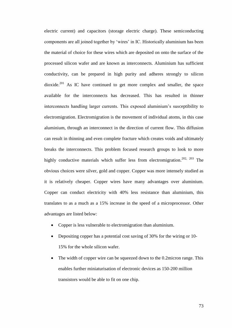
73
electric current) and capacitors (storage electric charge). These semiconducting
components are all joined together by ‘wires’ in IC. Historically aluminium has been
the material of choice for these wires which are deposited on onto the surface of the
processed silicon wafer and are known as interconnects. Aluminium has sufficient
conductivity, can be prepared in high purity and adheres strongly to silicon
dioxide.201
As IC have continued to get more complex and smaller, the space
available for the interconnects has decreased. This has resulted in thinner
interconnects handling larger currents. This exposed aluminium’s susceptibility to
electromigration. Electromigration is the movement of individual atoms, in this case
aluminium, through an interconnect in the direction of current flow. This diffusion
can result in thinning and even complete fracture which creates voids and ultimately
breaks the interconnects. This problem focused research groups to look to more
highly conductive materials which suffer less from electromigration.202, 203
The
obvious choices were silver, gold and copper. Copper was more intensely studied as
it is relatively cheaper. Copper wires have many advantages over aluminium.
Copper can conduct electricity with 40% less resistance than aluminium, this
translates to as a much as a 15% increase in the speed of a microprocessor. Other
advantages are listed below:
Copper is less vulnerable to electromigration than aluminium.
Depositing copper has a potential cost saving of 30% for the wiring or 10-
15% for the whole silicon wafer.
The width of copper wire can be squeezed down to the 0.2micron range. This
enables further miniaturisation of electronic devices as 150-200 million
transistors would be able to fit on one chip.
74
There are some disadvantages to using copper, it has an increased rate of diffusion
into silicon which can result in device malfunction.201
Also, copper does not adhere
to silicon as well as aluminium. These problems can be overcome with additional
processing steps to form a layer between the copper and silicon to act as a barrier
layer and also to increase adhesion.
For the current technology aluminium is deposited over the entire wafer and then
patterned by a process known as reactive ion etching (RIE), unwanted metal is then
etched away. Trials to pattern copper by this RIE method failed. This led to the need
for a new process to deposit high purity copper.204
Various forms of physical vapour
deposition (PVD) including sputtering, CVD and electroless plating were trialled.205
Covering trench walls was difficult with PVD whilst CVD grew conformal films
which leaves a seam in the middle of the trench.206
The Damascene Process, shown
schematically in Figure 32 , was first developed by IBM engineers, and provided a
solution which led to the mass production of copper wired IC in 1998.
Figure 32 A schematic of the Damascene process. 204
This process has three main steps:
Step 1: Growth of a smooth, continuous, conformal barrier layer onto the dielectric
material via ionized PVD, followed by a copper seed layer grown via ionized PVD
or CVD.
75
Step 2: The pattern is then filled using electroplating (electrolysis of copper ions
from solution onto the seed layer).
Step 3: Chemical mechanical polishing (CMP) is used to remove excess copper and
to planerise the wafer.
Although this method provided some way of incorporating copper interconnects, the
continued drive for reduction in size and increase in speed of IC, led to multilevel
ICs. The interconnects are then subsequently joined by vias (small opening in an
insulating oxide layer that allows a conductive connection between different layers).
As the height of the via increases, the width remains the same leading to an increase
in aspect ratio. As PVD is a line of sight technique, these high aspect ratio structures
have poor step coverage. Copper deposited by this method has the potential to build
up at the entrance to the via blocking any deposition at the base. Ideally, ALD would
be the technique of choice to overcome the issue of the difficulty in depositing
conformal layers with high aspect ratios. This research looks to the development of
an ALD process for the deposition of copper metal using different precursors with a
series of potential co-reagents. The experimental work and results are discussed in
Chapter 5.
2.2.3 Basic Properties of Copper Oxides
2.2.3.1 Crystal Structure
The crystal structure of both forms of copper oxide are shown in Figure 33. The unit
cell of cuprous oxide, Cu2O, contains 4 copper atoms and 2 oxygen atoms, with a
lattice constant of 4.2696Å.207
The unit cell is a body centered cubic lattice of
oxygen ions, in which each oxygen ion occupies the center of a tetrahedron formed
by copper ions, whilst the copper atoms arrange in a face centered cubic sublattice.
The molar mass of Cu2O is 143.09g/mol and it’s melting and boiling points are
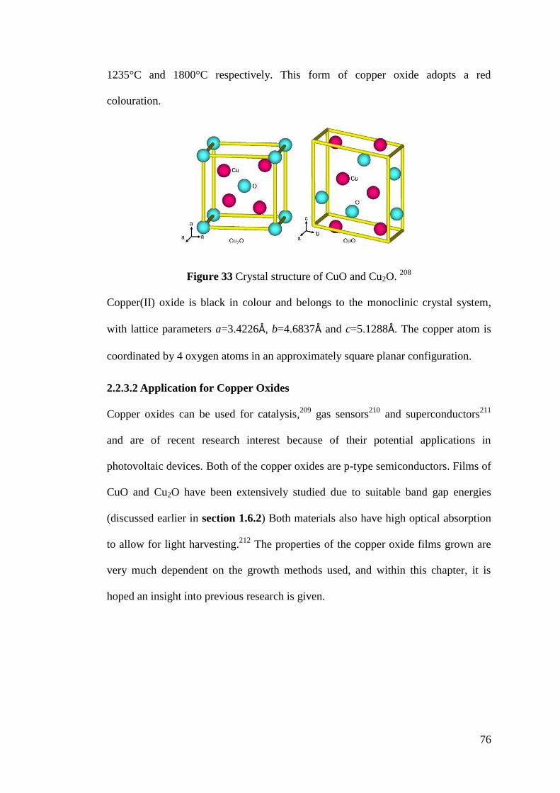
76
1235°C and 1800°C respectively. This form of copper oxide adopts a red
colouration.
Figure 33 Crystal structure of CuO and Cu2O. 208
Copper(II) oxide is black in colour and belongs to the monoclinic crystal system,
with lattice parameters a=3.4226Å, b=4.6837Å and c=5.1288Å. The copper atom is
coordinated by 4 oxygen atoms in an approximately square planar configuration.
2.2.3.2 Application for Copper Oxides
Copper oxides can be used for catalysis,209
gas sensors210
and superconductors211
and are of recent research interest because of their potential applications in
photovoltaic devices. Both of the copper oxides are p-type semiconductors. Films of
CuO and Cu2O have been extensively studied due to suitable band gap energies
(discussed earlier in section 1.6.2) Both materials also have high optical absorption
to allow for light harvesting.212
The properties of the copper oxide films grown are
very much dependent on the growth methods used, and within this chapter, it is
hoped an insight into previous research is given.
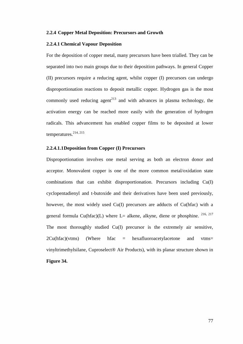
77
2.2.4 Copper Metal Deposition: Precursors and Growth
2.2.4.1 Chemical Vapour Deposition
For the deposition of copper metal, many precursors have been trialled. They can be
separated into two main groups due to their deposition pathways. In general Copper
(II) precursors require a reducing agent, whilst copper (I) precursors can undergo
disproportionation reactions to deposit metallic copper. Hydrogen gas is the most
commonly used reducing agent213
and with advances in plasma technology, the
activation energy can be reached more easily with the generation of hydrogen
radicals. This advancement has enabled copper films to be deposited at lower
temperatures.214, 215
2.2.4.1.1 Deposition from Copper (I) Precursors
Disproportionation involves one metal serving as both an electron donor and
acceptor. Monovalent copper is one of the more common metal/oxidation state
combinations that can exhibit disproportionation. Precursors including Cu(I)
cyclopentadienyl and t-butoxide and their derivatives have been used previously,
however, the most widely used Cu(I) precursors are adducts of Cu(hfac) with a
general formula Cu(hfac)(L) where L= alkene, alkyne, diene or phosphine. 216, 217
The most thoroughly studied Cu(I) precursor is the extremely air sensitive,
2Cu(hfac)(vtms) (Where hfac = hexafluoroacetylacetone and vtms=
vinyltrimethylsilane, Cuproselect® Air Products), with its planar structure shown in
Figure 34.
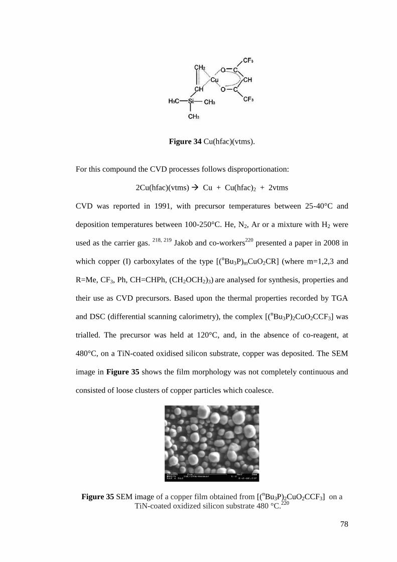
78
Figure 34 Cu(hfac)(vtms).
For this compound the CVD processes follows disproportionation:
2Cu(hfac)(vtms) Cu + Cu(hfac)2 + 2vtms
CVD was reported in 1991, with precursor temperatures between 25-40°C and
deposition temperatures between 100-250°C. He, N2, Ar or a mixture with H2 were
used as the carrier gas. 218, 219
Jakob and co-workers220
presented a paper in 2008 in
which copper (I) carboxylates of the type [(nBu3P)mCuO2CR] (where m=1,2,3 and
R=Me, CF3, Ph, CH=CHPh, (CH2OCH2)3) are analysed for synthesis, properties and
their use as CVD precursors. Based upon the thermal properties recorded by TGA
and DSC (differential scanning calorimetry), the complex [(nBu3P)2CuO2CCF3] was
trialled. The precursor was held at 120°C, and, in the absence of co-reagent, at
480°C, on a TiN-coated oxidised silicon substrate, copper was deposited. The SEM
image in Figure 35 shows the film morphology was not completely continuous and
consisted of loose clusters of copper particles which coalesce.
Figure 35 SEM image of a copper film obtained from [(nBu3P)2CuO2CCF3] on a
TiN-coated oxidized silicon substrate 480 °C.220
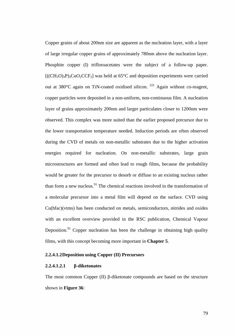
79
Copper grains of about 200nm size are apparent as the nucleation layer, with a layer
of large irregular copper grains of approximately 780nm above the nucleation layer.
Phosphite copper (I) trifloroacetates were the subject of a follow-up paper.
[((CH3O)3P)3CuO2CCF3] was held at 65°C and deposition experiments were carried
out at 380°C again on TiN-coated oxidised silicon. 221
Again without co-reagent,
copper particles were deposited in a non-uniform, non-continuous film. A nucleation
layer of grains approximately 200nm and larger particulates closer to 1200nm were
observed. This complex was more suited than the earlier proposed precursor due to
the lower transportation temperature needed. Induction periods are often observed
during the CVD of metals on non-metallic substrates due to the higher activation
energies required for nucleation. On non-metallic substrates, large grain
microstructures are formed and often lead to rough films, because the probability
would be greater for the precursor to desorb or diffuse to an existing nucleus rather
than form a new nucleus.91
The chemical reactions involved in the transformation of
a molecular precursor into a metal film will depend on the surface. CVD using
Cu(hfac)(vtms) has been conducted on metals, semiconductors, nitrides and oxides
with an excellent overview provided in the RSC publication, Chemical Vapour
Deposition.91
Copper nucleation has been the challenge in obtaining high quality
films, with this concept becoming more important in Chapter 5.
2.2.4.1.2 Deposition using Copper (II) Precursors
2.2.4.1.2.1 β-diketonates
The most common Copper (II) β-diketonate compounds are based on the structure
shown in Figure 36:
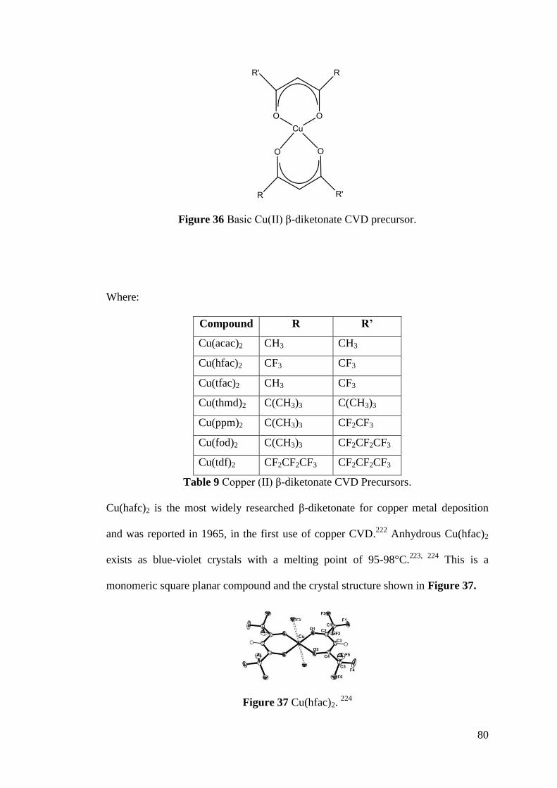
80
Figure 36 Basic Cu(II) β-diketonate CVD precursor.
Where:
Compound R R’
Cu(acac)2 CH3 CH3
Cu(hfac)2 CF3 CF3
Cu(tfac)2 CH3 CF3
Cu(thmd)2 C(CH3)3 C(CH3)3
Cu(ppm)2 C(CH3)3 CF2CF3
Cu(fod)2 C(CH3)3 CF2CF2CF3
Cu(tdf)2 CF2CF2CF3 CF2CF2CF3
Table 9 Copper (II) β-diketonate CVD Precursors.
Cu(hafc)2 is the most widely researched β-diketonate for copper metal deposition
and was reported in 1965, in the first use of copper CVD.222
Anhydrous Cu(hfac)2
exists as blue-violet crystals with a melting point of 95-98°C.223, 224
This is a
monomeric square planar compound and the crystal structure shown in Figure 37.
Figure 37 Cu(hfac)2. 224
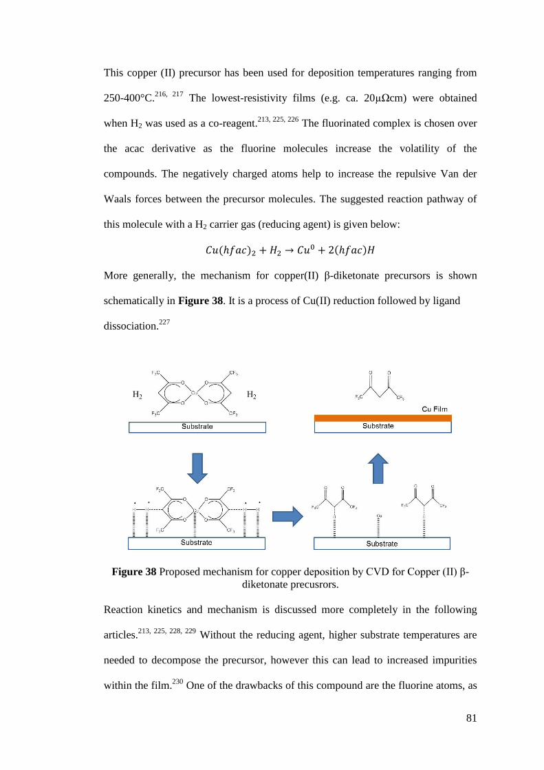
81
This copper (II) precursor has been used for deposition temperatures ranging from
250-400°C.216, 217
The lowest-resistivity films (e.g. ca. 20µΩcm) were obtained
when H2 was used as a co-reagent.213, 225, 226
The fluorinated complex is chosen over
the acac derivative as the fluorine molecules increase the volatility of the
compounds. The negatively charged atoms help to increase the repulsive Van der
Waals forces between the precursor molecules. The suggested reaction pathway of
this molecule with a H2 carrier gas (reducing agent) is given below:
( ) ( )
More generally, the mechanism for copper(II) β-diketonate precursors is shown
schematically in Figure 38. It is a process of Cu(II) reduction followed by ligand
dissociation.227
Figure 38 Proposed mechanism for copper deposition by CVD for Copper (II) β-
diketonate precusrors.
Reaction kinetics and mechanism is discussed more completely in the following
articles.213, 225, 228, 229
Without the reducing agent, higher substrate temperatures are
needed to decompose the precursor, however this can lead to increased impurities
within the film.230
One of the drawbacks of this compound are the fluorine atoms, as
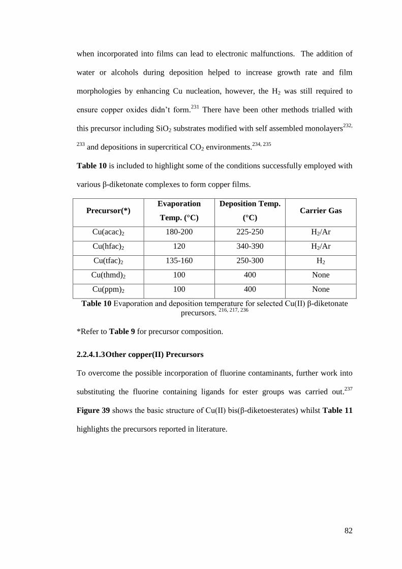
82
when incorporated into films can lead to electronic malfunctions. The addition of
water or alcohols during deposition helped to increase growth rate and film
morphologies by enhancing Cu nucleation, however, the H2 was still required to
ensure copper oxides didn’t form.231
There have been other methods trialled with
this precursor including SiO2 substrates modified with self assembled monolayers232,
233 and depositions in supercritical CO2 environments.
234, 235
Table 10 is included to highlight some of the conditions successfully employed with
various β-diketonate complexes to form copper films.
Precursor(*) Evaporation
Temp. (°C)
Deposition Temp.
(°C) Carrier Gas
Cu(acac)2 180-200 225-250 H2/Ar
Cu(hfac)2 120 340-390 H2/Ar
Cu(tfac)2 135-160 250-300 H2
Cu(thmd)2 100 400 None
Cu(ppm)2 100 400 None
Table 10 Evaporation and deposition temperature for selected Cu(II) β-diketonate
precursors. 216, 217, 236
*Refer to Table 9 for precursor composition.
2.2.4.1.3 Other copper(II) Precursors
To overcome the possible incorporation of fluorine contaminants, further work into
substituting the fluorine containing ligands for ester groups was carried out.237
Figure 39 shows the basic structure of Cu(II) bis(β-diketoesterates) whilst Table 11
highlights the precursors reported in literature.
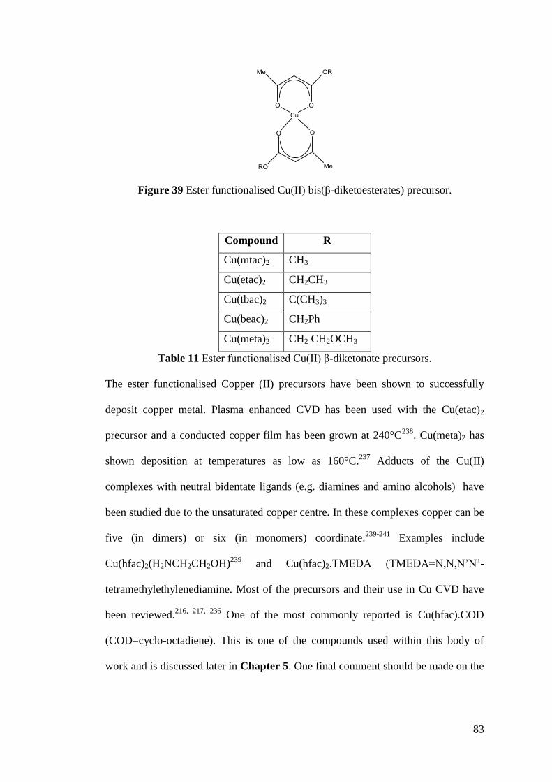
83
Figure 39 Ester functionalised Cu(II) bis(β-diketoesterates) precursor.
Compound R
Cu(mtac)2 CH3
Cu(etac)2 CH2CH3
Cu(tbac)2 C(CH3)3
Cu(beac)2 CH2Ph
Cu(meta)2 CH2 CH2OCH3
Table 11 Ester functionalised Cu(II) β-diketonate precursors.
The ester functionalised Copper (II) precursors have been shown to successfully
deposit copper metal. Plasma enhanced CVD has been used with the Cu(etac)2
precursor and a conducted copper film has been grown at 240°C238
. Cu(meta)2 has
shown deposition at temperatures as low as 160°C.237
Adducts of the Cu(II)
complexes with neutral bidentate ligands (e.g. diamines and amino alcohols) have
been studied due to the unsaturated copper centre. In these complexes copper can be
five (in dimers) or six (in monomers) coordinate.239-241
Examples include
Cu(hfac)2(H2NCH2CH2OH)239
and Cu(hfac)2.TMEDA (TMEDA=N,N,N’N’-
tetramethylethylenediamine. Most of the precursors and their use in Cu CVD have
been reviewed.216, 217, 236
One of the most commonly reported is Cu(hfac).COD
(COD=cyclo-octadiene). This is one of the compounds used within this body of
work and is discussed later in Chapter 5. One final comment should be made on the
84
recent interest seen in the development of amino-alkoxides242-247
, although
incorporation of imprurties and and high resistivites leave room for development.
2.2.4.2 Atomic Layer Deposition
2.2.4.2.1 Deposition from Copper (I) Precursors
Juppo at el trialled copper ALD using copper chloride followed by a reduction with
zinc to give Cu(0). 215
For this method high temperatures of 400°C, together with
films contaminated with zinc, highlighted its inadequecies for the micorelectroncis
industry. The use of copper chloride, with hydrogen gas as the reducing agent,
removed the zinc contaminate, but still, high temperatures of 300-400°C where
required due to the low volatility of CuCl.248
For both experiments, rough films
where afforded. A copper (I) β-diketonate compound, namely [(nBu3P)2Cu(acac)]
has been investigated by Mueller et al. 249
With a co-reagent of a mixture of water
vapour and oxygen, and temperatures between 100 and 130°C, this study looked to
the reduction of copper oxide films to copper metal. This was to look at the
suitablity for forming copper seedlayers on ruthenium. Again, the complexity of the
prcoess would make it unsuitable for large scale production.
Cu(I) amidinates, have been investigated.70, 250, 251
Dimeric [Cu(RNC)(CH3)NR)]2,
(where R=isopropyl), with a hydrogen co-reagent showed no deposition below
180°C. At 250°C crystallites were formed and the lack of a uniform thin film
hindred futher work with this precursor. Cu(I) N,N-di-sec-butylacetamidinate
(Figure 40) was found to be the most suitable amidinate complex for Cu ALD.252
It
has a melting point of 77°C and reactive towards a H2 reducing agent.
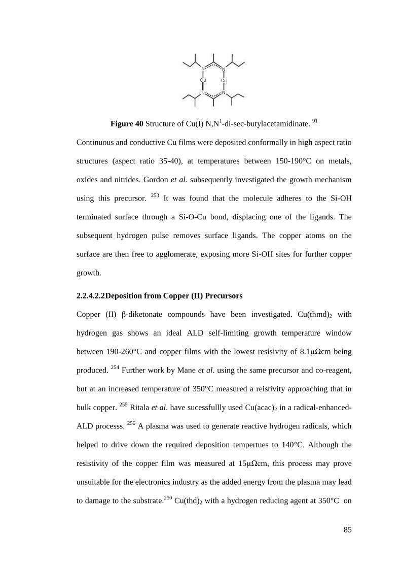
85
Figure 40 Structure of Cu(I) N,N1-di-sec-butylacetamidinate.
91
Continuous and conductive Cu films were deposited conformally in high aspect ratio
structures (aspect ratio 35-40), at temperatures between 150-190°C on metals,
oxides and nitrides. Gordon et al. subsequently investigated the growth mechanism
using this precursor. 253
It was found that the molecule adheres to the Si-OH
terminated surface through a Si-O-Cu bond, displacing one of the ligands. The
subsequent hydrogen pulse removes surface ligands. The copper atoms on the
surface are then free to agglomerate, exposing more Si-OH sites for further copper
growth.
2.2.4.2.2 Deposition from Copper (II) Precursors
Copper (II) β-diketonate compounds have been investigated. Cu(thmd)2 with
hydrogen gas shows an ideal ALD self-limiting growth temperature window
between 190-260°C and copper films with the lowest resisivity of 8.1µΩcm being
produced. 254
Further work by Mane et al. using the same precursor and co-reagent,
but at an increased temperature of 350°C measured a reistivity approaching that in
bulk copper. 255
Ritala et al. have sucessfullly used Cu(acac)2 in a radical-enhanced-
ALD processs. 256
A plasma was used to generate reactive hydrogen radicals, which
helped to drive down the required deposition tempertues to 140°C. Although the
resistivity of the copper film was measured at 15µΩcm, this process may prove
unsuitable for the electronics industry as the added energy from the plasma may lead
to damage to the substrate.250
Cu(thd)2 with a hydrogen reducing agent at 350°C on
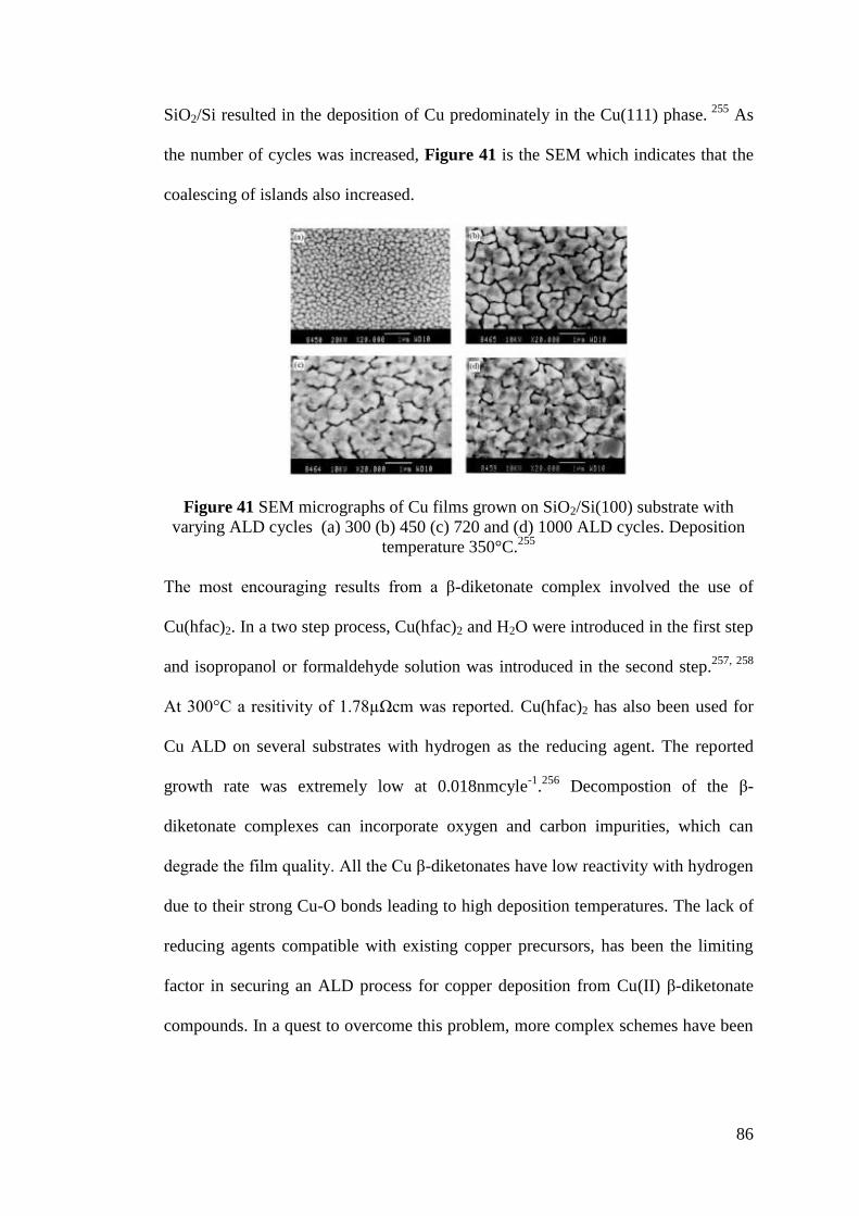
86
SiO2/Si resulted in the deposition of Cu predominately in the Cu(111) phase. 255
As
the number of cycles was increased, Figure 41 is the SEM which indicates that the
coalescing of islands also increased.
Figure 41 SEM micrographs of Cu films grown on SiO2/Si(100) substrate with
varying ALD cycles (a) 300 (b) 450 (c) 720 and (d) 1000 ALD cycles. Deposition
temperature 350°C.255
The most encouraging results from a β-diketonate complex involved the use of
Cu(hfac)2. In a two step process, Cu(hfac)2 and H2O were introduced in the first step
and isopropanol or formaldehyde solution was introduced in the second step.257, 258
At 300°C a resitivity of 1.78µΩcm was reported. Cu(hfac)2 has also been used for
Cu ALD on several substrates with hydrogen as the reducing agent. The reported
growth rate was extremely low at 0.018nmcyle-1
.256
Decompostion of the β-
diketonate complexes can incorporate oxygen and carbon impurities, which can
degrade the film quality. All the Cu β-diketonates have low reactivity with hydrogen
due to their strong Cu-O bonds leading to high deposition temperatures. The lack of
reducing agents compatible with existing copper precursors, has been the limiting
factor in securing an ALD process for copper deposition from Cu(II) β-diketonate
compounds. In a quest to overcome this problem, more complex schemes have been
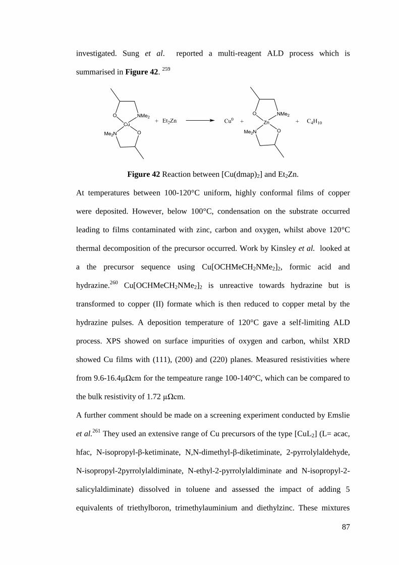
87
investigated. Sung et al. reported a multi-reagent ALD process which is
summarised in Figure 42. 259
Figure 42 Reaction between [Cu(dmap)2] and Et2Zn.
At temperatures between 100-120°C uniform, highly conformal films of copper
were deposited. However, below 100°C, condensation on the substrate occurred
leading to films contaminated with zinc, carbon and oxygen, whilst above 120°C
thermal decomposition of the precursor occurred. Work by Kinsley et al. looked at
a the precursor sequence using Cu[OCHMeCH2NMe2]2, formic acid and
hydrazine.260
Cu[OCHMeCH2NMe2]2 is unreactive towards hydrazine but is
transformed to copper (II) formate which is then reduced to copper metal by the
hydrazine pulses. A deposition temperature of 120°C gave a self-limiting ALD
process. XPS showed on surface impurities of oxygen and carbon, whilst XRD
showed Cu films with (111), (200) and (220) planes. Measured resistivities where
from 9.6-16.4µΩcm for the tempeature range 100-140°C, which can be compared to
the bulk resistivity of 1.72 µΩcm.
A further comment should be made on a screening experiment conducted by Emslie
et al.261
They used an extensive range of Cu precursors of the type [CuL2] (L= acac,
hfac, N-isopropyl-β-ketiminate, N,N-dimethyl-β-diketiminate, 2-pyrrolylaldehyde,
N-isopropyl-2pyrrolylaldiminate, N-ethyl-2-pyrrolylaldiminate and N-isopropyl-2-
salicylaldiminate) dissolved in toluene and assessed the impact of adding 5
equivalents of triethylboron, trimethylauminium and diethylzinc. These mixtures
88
were then subjected to temperatures of 25, 50, 75, 100 and 120°C for 24 hours. A
copper precipitate was found for each solution. When this was repeated in the
presence of substrates, copper films with varying amounts of carbon, oxygen, boron,
zinc and aluminium were afforded. Films produced with diethylzinc at 120-150°C
showed most promise, but the high contamination gave a resitivity of 89µΩcm.
2.2.5 Copper Deposition for this research
From the earlier sections, it is apparent that copper metal deposition via ALD has
still not been successfully achieved for industry requirements. A controllable low
temperature process producing conformal, uniform, dense conductive copper films
is required. SAFC Hitech formed a collaboration with the University of Bath which
looked to develop complexes of the type [CpM(L)]. This has remained a less studied
area of copper chemistry. For a comprehensive background of the chemistry and
precursors chosen please refer to Willcocks’ thesis.202
ALD precursors have historically incorporated the Cp ligand, with many
metallocene-type complexes giving high volatility and themal stability. This
inherent stability is due the fact that the Cp ligands occupies 3 potential co-
ordination sites and can bind to a metal centre through multiple molecular orbitals. It
is also generally inert to electrophilic and nucleophilic attack. Cu(I) has a full d
shell, so any ligand interactions are with the empty 4s and 4p orbital. Cu(II)
complexes are less stable, it has 9 d-electrons in its outer shell which can be easily
reduced. This can occur via two routes:
A one-electron process with the formation of Cu(I)-R species and a radical
species
A two-electron reductive elimination process with the formation of Cu(0)
and a R-R species.
89
The instability from the Cu(II) complexes, means that they were discounted as
possible ALD sources, by the colloborators at the University of Bath. For Cu(I) the
Cp adopts an Ƞ5
bonding mode. In the notation, [CpM(L)], L can be used to
represent a ơ-donating ligand. Isocyanides, -RNC ligands are known to form stable
organometallic complexes. The resonance form for the RNC group is between a
double and a triple bond. The lone pair of electrons available for metal coordination
resides in the non-bonding orbital of the carbon atom. For this body of work, a
Cu(II) β-diketonate [Cu(hfac)(COD)] and a Cu(I) complex namely CpCu(tBuNC)
are compared. The co-reagents trialled were tertiary butylhydrazine and hydrogen
plasma. A discussion is provided on chemical synthesis and characterisation, as well
as subsequent film growth. ALD and CVD methods were trialled on multiple
substrates.
2.2.6 Copper Oxide Deposition: Precursors and Growth
Although much work has been devoted to the growth of metallic copper thin films
by ALD and CVD, very little attention has focused on the growth of copper oxides,
adding further weight to the need to develop a copper precursor suitable for the
conformal deposition of p-type Cu2O material for structured PV devices.
2.2.6.1 Chemical Vapour Deposition
To achieve the aim of finding a copper precursor suitable for the ALD of copper
oxides, a study of the prior literature for the deposition of copper oxides has been
carried out and is detailed in the following section.
90
2.2.6.1.1 Copper (I) Precursors
2.2.6.1.1.1 Copper (I) oxide:Cu2O
Developement for copper oxide precursors has been ongoing. In 1993, Cu(I)
complexes with trimethyl phosphite, P(OMe)3, and aliphatic perfluorinated
carboxylates (RCOO) of the type [Cu2(P(OMe)3)2(µ-RCOO)2] where R=CF3, C2F5,
C3F7, C6F13, C7F15, C8F17, C9F19 have been prepared.262
Although no growth data has
been presented, [Cu2(P(OMe)3)2(µ-C6F13COO)2] was suggested as the most suitable
based upon thermal anlaysis. A complex like this is less likely to be used in the
electronics industry due to manufacturing time and costs. The inclusion of P and F
atoms also has the potential for film contamination.
The tetrameric alkoxide precursor, copper (I) tertiary butoxide, (Cu(OtBu)4, has been
reported by Jefferies et al.263
It has a vapour pressure which is much lower than that
of the copper β-diketonates as its sublimes at 110°C at 10-4
Torr. At 237°C on
borosilicate glass, a film analysed by XRD as Cu2O was deposited simply by
passing the precursor over the heated substrate without co-reactant. Unfortunately,
on SEM analysis, the deposited material was a mass of whiskers 0.5-0.75µm thick
and upto 35µm long. The whiskers were not well adhered to the substrate. This poor
film coverage and the low volatility of the precursor make it an unlikely source for
use in industry. Interestingly, at higher temperatures, closer to 400°C, Cu metal can
be deposited from this precursor, although, this too has poor film coverage, with
copper island formation.
2.2.6.1.1.2 Copper (II) oxide:CuO
Copper chloride with an alternate supply of O2/H2O as the oxidant has been
successfully used to deposit copper (II) oxide264
on a MgO (100) substrate at 410°C.
The XRD pattern shows the expected diffractions for CuO(111) and CuO(222).
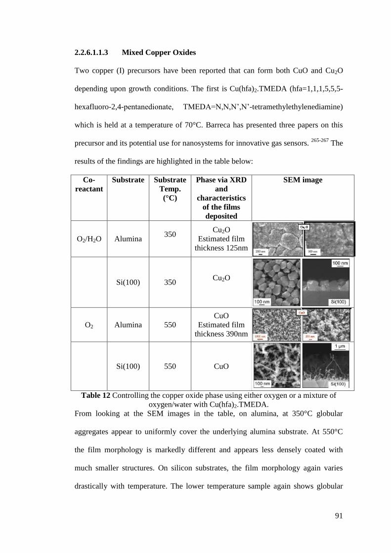
91
2.2.6.1.1.3 Mixed Copper Oxides
Two copper (I) precursors have been reported that can form both CuO and Cu2O
depending upon growth conditions. The first is Cu(hfa)2.TMEDA (hfa=1,1,1,5,5,5-
hexafluoro-2,4-pentanedionate, TMEDA=N,N,N’,N’-tetramethylethylenediamine)
which is held at a temperature of 70°C. Barreca has presented three papers on this
precursor and its potential use for nanosystems for innovative gas sensors. 265-267
The
results of the findings are highlighted in the table below:
Co-
reactant
Substrate Substrate
Temp.
(°C)
Phase via XRD
and
characteristics
of the films
deposited
SEM image
O2/H2O Alumina 350
Cu2O
Estimated film
thickness 125nm
Si(100) 350 Cu2O
O2 Alumina 550
CuO
Estimated film
thickness 390nm
Si(100) 550 CuO
Table 12 Controlling the copper oxide phase using either oxygen or a mixture of
oxygen/water with Cu(hfa)2.TMEDA.
From looking at the SEM images in the table, on alumina, at 350°C globular
aggregates appear to uniformly cover the underlying alumina substrate. At 550°C
the film morphology is markedly different and appears less densely coated with
much smaller structures. On silicon substrates, the film morphology again varies
drastically with temperature. The lower temperature sample again shows globular
92
growth but has an increased number of voids when compared to the alumina sample.
At the higher temperature a much more open structure of nanowires is observed, and
this is attributed to a higher surface mobility. The side branches are formed due to
lattice stresses. Once again, the poor coverage of the substrates would limit its use in
industry.
The second precursor is copper (I) iodide. Hong268
and later Ottosson269
detail
experimental work with O2 and O2/N2O oxidants respectively. Hong studied the
effects of reactant concentration, reaction tempertures, reactor diameter and total
reactor pressure on the growth rate. He reported the film growth observed on the
walls of the reactor when deposition temperatures of 600, 700, 800°C were used.
Interestingly, the species of copper oxide formed changed as the distance from the
precursor inlet increased. At the inlet, a dense Cu2O (111) film was formed, whilst
downstream, a porous Cu2O and CuO film was detected by SEM/XRD. Ottosson
carried out similar work to investigate the parameters that control the phase stability
based on earlier publications. CuI was heated to 500°C was reacted with O2 or N2O
or a mixture of Ar + O2(N2O). The impact of altering the oxygen partial pressure is
summarised in Table 13.
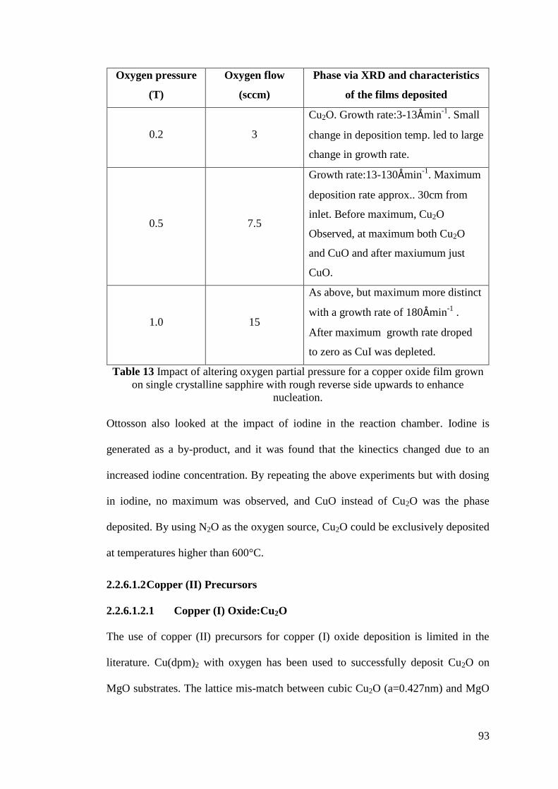
93
Oxygen pressure
(T)
Oxygen flow
(sccm)
Phase via XRD and characteristics
of the films deposited
0.2 3
Cu2O. Growth rate:3-13Åmin-1
. Small
change in deposition temp. led to large
change in growth rate.
0.5 7.5
Growth rate:13-130Åmin-1
. Maximum
deposition rate approx.. 30cm from
inlet. Before maximum, Cu2O
Observed, at maximum both Cu2O
and CuO and after maxiumum just
CuO.
1.0 15
As above, but maximum more distinct
with a growth rate of 180Åmin-1
.
After maximum growth rate droped
to zero as CuI was depleted.
Table 13 Impact of altering oxygen partial pressure for a copper oxide film grown
on single crystalline sapphire with rough reverse side upwards to enhance
nucleation.
Ottosson also looked at the impact of iodine in the reaction chamber. Iodine is
generated as a by-product, and it was found that the kinectics changed due to an
increased iodine concentration. By repeating the above experiments but with dosing
in iodine, no maximum was observed, and CuO instead of Cu2O was the phase
deposited. By using N2O as the oxygen source, Cu2O could be exclusively deposited
at temperatures higher than 600°C.
2.2.6.1.2 Copper (II) Precursors
2.2.6.1.2.1 Copper (I) Oxide:Cu2O
The use of copper (II) precursors for copper (I) oxide deposition is limited in the
literature. Cu(dpm)2 with oxygen has been used to successfully deposit Cu2O on
MgO substrates. The lattice mis-match between cubic Cu2O (a=0.427nm) and MgO
94
(a=0.422nm) is small, therefore MgO should be suited for the growth of high quality
Cu2O thin films. The crystallinity of the films grown increased with increasing
deposition temperature, with the temperature range from 675-800°C investigated. At
790°C a growth rate of 0.25Å/s was achieved and a film morphology of islands
ranging btween 300-500nm in diameter. At a lower temperature of 690°C the islands
are 500nm in size and in contact with one another except where micropores are
present.
2.2.6.1.2.2 Copper (II) Oxide:CuO
Solvated Cu(thd)2 has been used as a single-source CVD precursor. Klippe et al.
documented a process by which the precursor solution is kept outside of the vacuum
system in a reservoir. 270
It is then dosed into the reactor via a mass flow controller
and exposed to temperatures of 60°C to flash evaporate the solvent. Over the
deposition temperature of 225-700°C CuO layers were deposited. Another β-
diketonate precursor, Cu(hfac)2, was very recently reported by Koh.271
A variant on
a CVD process, a high pressure micro-plasma jet system was used. The aim of this
study was to analyse CuO nanostructures. With a N2 co-reagent, vertically aligned
monocrystalline CuO nanowires were grown on silicon with a growth rate of
~120nm/min. Conversely, when oxygen gas was used, there was a drastic change in
film morphology, to larger diameter wires, with spiral like formations suggesting
screw dislocation growth.
2.2.6.1.2.3 Mixed Copper Oxides
Copper β-diketonates have been used most widely in the deposition of copper oxide,
although the resulting films are often mixed phase oxides. Cu(acac)2 held at 175°C
and used with oxygen was used to deposit onto MgO (good lattice match) an Al2O3
(cheap, transparent and standard) substrates.272
They report no film growth below
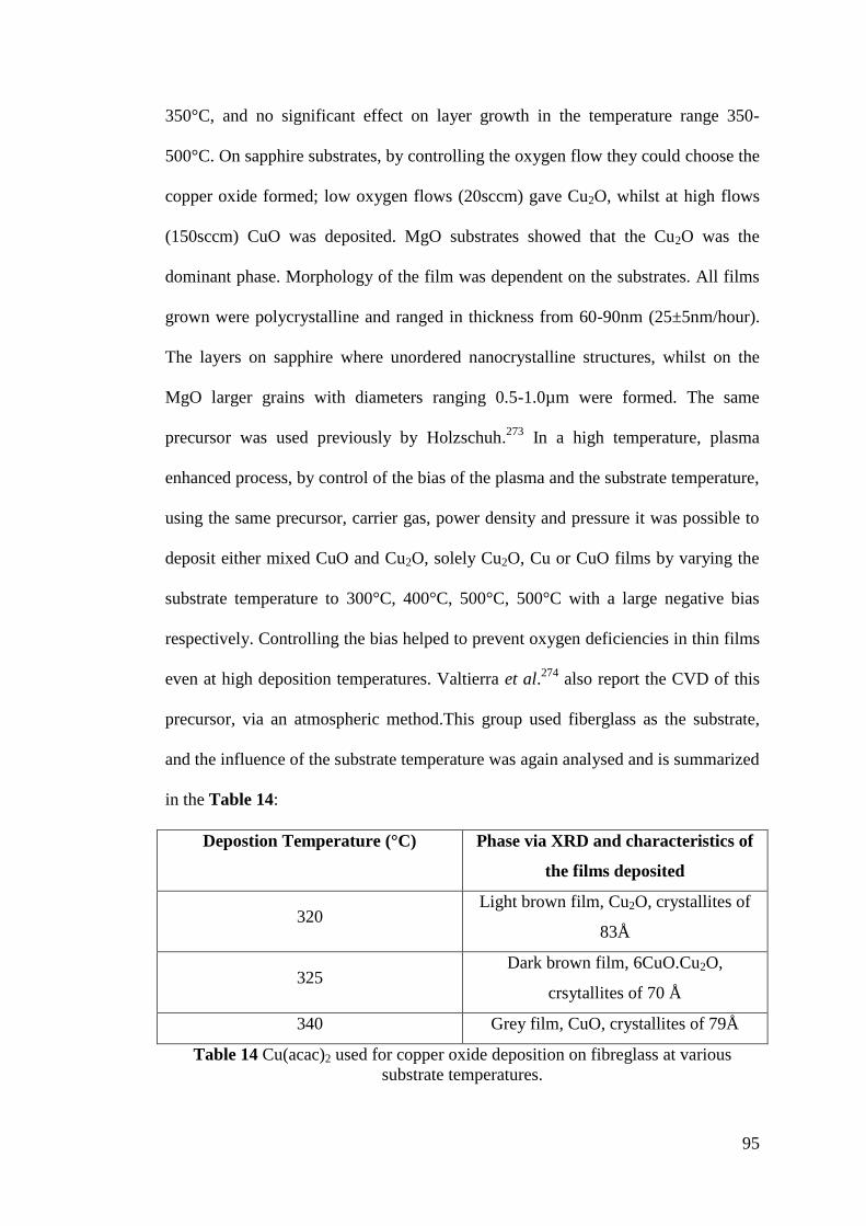
95
350°C, and no significant effect on layer growth in the temperature range 350-
500°C. On sapphire substrates, by controlling the oxygen flow they could choose the
copper oxide formed; low oxygen flows (20sccm) gave Cu2O, whilst at high flows
(150sccm) CuO was deposited. MgO substrates showed that the Cu2O was the
dominant phase. Morphology of the film was dependent on the substrates. All films
grown were polycrystalline and ranged in thickness from 60-90nm (25±5nm/hour).
The layers on sapphire where unordered nanocrystalline structures, whilst on the
MgO larger grains with diameters ranging 0.5-1.0µm were formed. The same
precursor was used previously by Holzschuh.273
In a high temperature, plasma
enhanced process, by control of the bias of the plasma and the substrate temperature,
using the same precursor, carrier gas, power density and pressure it was possible to
deposit either mixed CuO and Cu2O, solely Cu2O, Cu or CuO films by varying the
substrate temperature to 300°C, 400°C, 500°C, 500°C with a large negative bias
respectively. Controlling the bias helped to prevent oxygen deficiencies in thin films
even at high deposition temperatures. Valtierra et al.274
also report the CVD of this
precursor, via an atmospheric method.This group used fiberglass as the substrate,
and the influence of the substrate temperature was again analysed and is summarized
in the Table 14:
Depostion Temperature (°C) Phase via XRD and characteristics of
the films deposited
320 Light brown film, Cu2O, crystallites of
83Å
325 Dark brown film, 6CuO.Cu2O,
crsytallites of 70 Å
340 Grey film, CuO, crystallites of 79Å
Table 14 Cu(acac)2 used for copper oxide deposition on fibreglass at various
substrate temperatures.
96
Interestingly, the group report the deposition of 6CuO.Cu2O from 330-340°C and
for this phase both SEM and AFM show uniform complete coverage of the fiber
glass with smooth and regular crystallites.
Maruyama investigated another β-diketonate precursor namely, Cu(thd)2 which was
held at 220°C. 275
Oxygen gas was used as the oxidant in an atmospheric pressure
CVD process. Borosilicate glass was used as the substrate and deposition trialled at
300 and 500°C. Similarly to the methods already described, the formation of Cu2O
or CuO was obtained by adjusting the oxygen partial pressure. At higher partial
pressures, monoclinic CuO formed, whilst at lower pressures, cubic Cu2O was
predominant. Interestingly the surface morphology for CuO alters with reaction
temperature. Whilst at 300°C the films exhibits a coarse three-dimensional network
structure, the film deposited at 500°C shows a much more 3D-like stack of angular
lumps.
A final copper source worth mentioning is aqueous cupric nitrate, Cu(NO3)2.276
A
flame assisted CVD process for a substrate temperature range of 100 and 400°C
enabled the deposition of copper oxide thin films. Again the film morphology is
dependent upon the susbtrate temperatures. At 200°C island growth with particle
diameters 102-173nm was observed. At 300°C the islands appeared to coalesce and
form a continuous film, which, by 400°C, has returned back to an island formation,
note though, this time with an increased particle size (229-323nm) but with a large
separation. The authors attribute this to mostly Cu2O at low temperatures and CuO
at higher temperatures which was confirmed by XRD. Mixed phase CuO copper was
detected at 200°C, mixed CuO/Cu2O at 300°C and by 400°C, only CuO reflections
were observed.
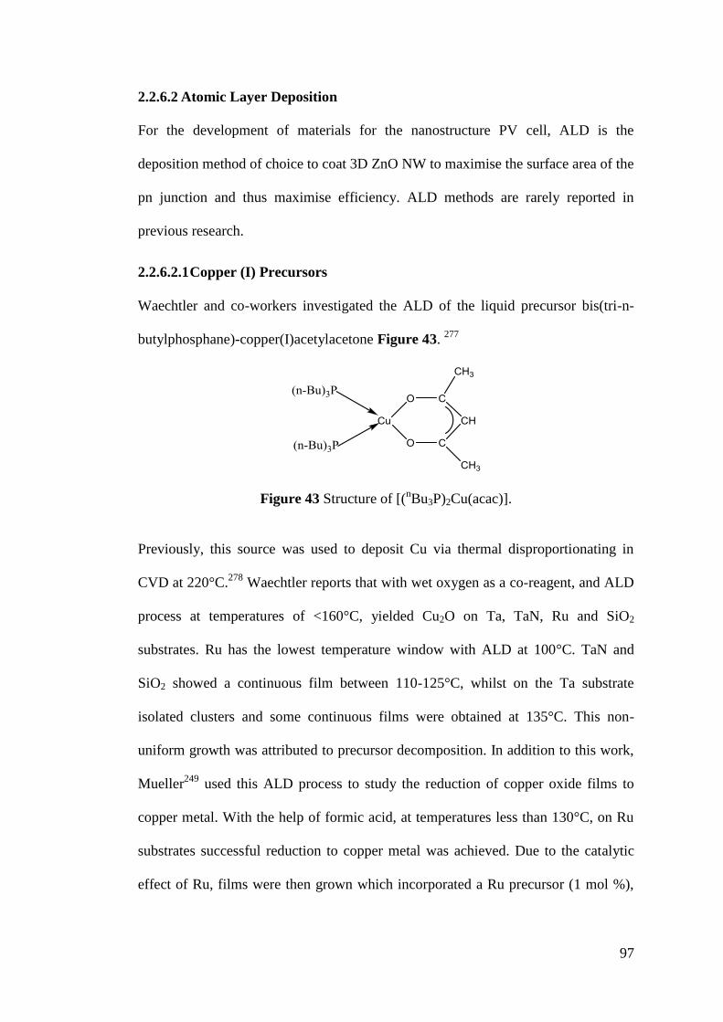
97
2.2.6.2 Atomic Layer Deposition
For the development of materials for the nanostructure PV cell, ALD is the
deposition method of choice to coat 3D ZnO NW to maximise the surface area of the
pn junction and thus maximise efficiency. ALD methods are rarely reported in
previous research.
2.2.6.2.1 Copper (I) Precursors
Waechtler and co-workers investigated the ALD of the liquid precursor bis(tri-n-
butylphosphane)-copper(I)acetylacetone Figure 43. 277
Figure 43 Structure of [(nBu3P)2Cu(acac)].
Previously, this source was used to deposit Cu via thermal disproportionating in
CVD at 220°C.278
Waechtler reports that with wet oxygen as a co-reagent, and ALD
process at temperatures of <160°C, yielded Cu2O on Ta, TaN, Ru and SiO2
substrates. Ru has the lowest temperature window with ALD at 100°C. TaN and
SiO2 showed a continuous film between 110-125°C, whilst on the Ta substrate
isolated clusters and some continuous films were obtained at 135°C. This non-
uniform growth was attributed to precursor decomposition. In addition to this work,
Mueller249
used this ALD process to study the reduction of copper oxide films to
copper metal. With the help of formic acid, at temperatures less than 130°C, on Ru
substrates successful reduction to copper metal was achieved. Due to the catalytic
effect of Ru, films were then grown which incorporated a Ru precursor (1 mol %),
98
[(Ƞ5-C5H4SiMe3)(Ƞ
5-C7H11)Ru], and used formic acid, to grow copper on a range of
substrates including TaN, Ni and Co.
Recent work by Muñoz-Rojas et al. reports the use of
(trimethylvinylsilyl)hexafluoroacetylacetonato copper(I), Cu(I)(hfac)(TMVS),
(CupraselectTM
Air Products and Chemicals Inc.) held at 65°C, with water as the
oxidizer.279
The substrates used were borosilicate glass at temperatures between 150
and 350°C and also plastic susbtrates (PEN films from Dupont) at 150 and 200°C.
The achieved growth rate was ~1nm.min-1
. Cu2O films were grown on both
substrates using atmospheric ALD in the temperature range of 150-225°C. The
application of copper (I) precursors in the deposition of CuO appeared lacking from
a literature survey.
2.2.6.2.2 Copper (II) Precursors
Copper (II) precursors are reported in literature for the deposition of CuO only, not
Cu2O. Alnes et al. have reported the use of Cu(acac)2 with ozone for the deposition
of copper (II) oxide.280
They report an ALD window of 150-230°C with a growth
rate of ~0.04nm/cycle, however the uniformity and surface roughness was much
better at lower temperatures.
2.2.7 Copper Oxide Deposition for this research
The copper precursors Cu(hfac)(COD) and CpCu(tBuNC) were used to try to
deposit copper oxide layers. Water, ozone and oxygen plasma were studied as co-
reagents. Chapter 5 presents the results from the experimental work.
2.2.8 Copper Oxide Nanowires
Although not directly relevant to the research here, like zinc oxide, nanostructures of
copper oxide can be deposited. Cuprous oxide (Cu2O) and cupric oxide (CuO)
99
nanowires have become more important in the study of energy conversion and
optoelectronic devices. Although the properties of these materials are well suited to
the end applications, large-bulk synthesis routes have yet to be established. A recent
review by Filipič and Cvelbar provides an extensive overview into copper oxide
nanowires and the growth methods employed. 281
The NWs can be produced using
different approaches e.g. wet chemical, electrochemical, hydrothermal and thermal
oxidation methods, and as such the NWs can have different lengths, diameters,
morphologies or even chemical composition. Copper oxide NWs can be Cu2O or
CuO, they can be single-crystalline, or polycrystalline or even a mixture of a
crystalline material with an amorphous sheath282
. For NWs to be incorporated into
commerical devices, they must be produced quickly, controllably and in large
quanitities. The advantages of NWs have been highlighted previously in Chapter 1.
The large surface area can lead to a higher absorption of photons in PV devices
which results in greater efficiency. Similarly, for sensors, the increased surface area
means a higher probability of species absorption which leads to a better response.
Cu2O nanowires have been reported to have a slightly higher band gap of 2.69eV
when compared to bulk thin film Cu2O at 2.2eV. This can be understood on the
basis of quantum size effect which arises due to a very small size of nanostructures
in one dimension.212
Copper oxides NW were not investigated as part of this study,
however, the possibility opens up the potential of inverting the system highlighted
previously in Figure 13 i.e. copper oxide nanowires conformally coated with a n-
type ZnO layer.
100
Chapter 3 Experimental Methods
3.1 Chemical Characterisation
3.1.1 1H Nuclear Magnetic Resonance (NMR)
NMR is a phenomenon that occurs when the nuclei in an atom are held in a static
magnetic field and exposed to a second oscillating field. Only nuclei with spin are
affected by the magnetic field. Protons, electrons and neutrons all have the spin
property, which comes in multiples of ½ and can be either plus or minus. For NMR
we look only to the nuclei of the atom, so in the case of 1H NMR, hydrogen (
1H)
has one proton resulting in a net spin of ½. In NMR it is the unpaired spin that is
important. When placed in a magnetic field of strength B, a particle with a net spin
can absorb a photon, of frequency ν. The frequency ν depends on the gyromagnetic
ratio (ratio of the magnetic dipole moment to the angular momentum), γ of the
particle,
Equation 22:
Nucleons fill orbitals like electrons, and as nucleons possess spin, they pair up as the
orbitals are filled and if there are two spins of opposite sign, they can cancel each
other out. When the nuclei are exposed to the external magnetic field, it can be
thought of as a magnet, the spin vector aligns with the magnetic field. The low
energy state is when the poles area aligned N-S-N-S and the high energy state is N-
N-S-S. A transition between the two energy states can occur on absorption of a
photon. The energy of the absorbed photon must exactly match that of the energy
difference in the two states.
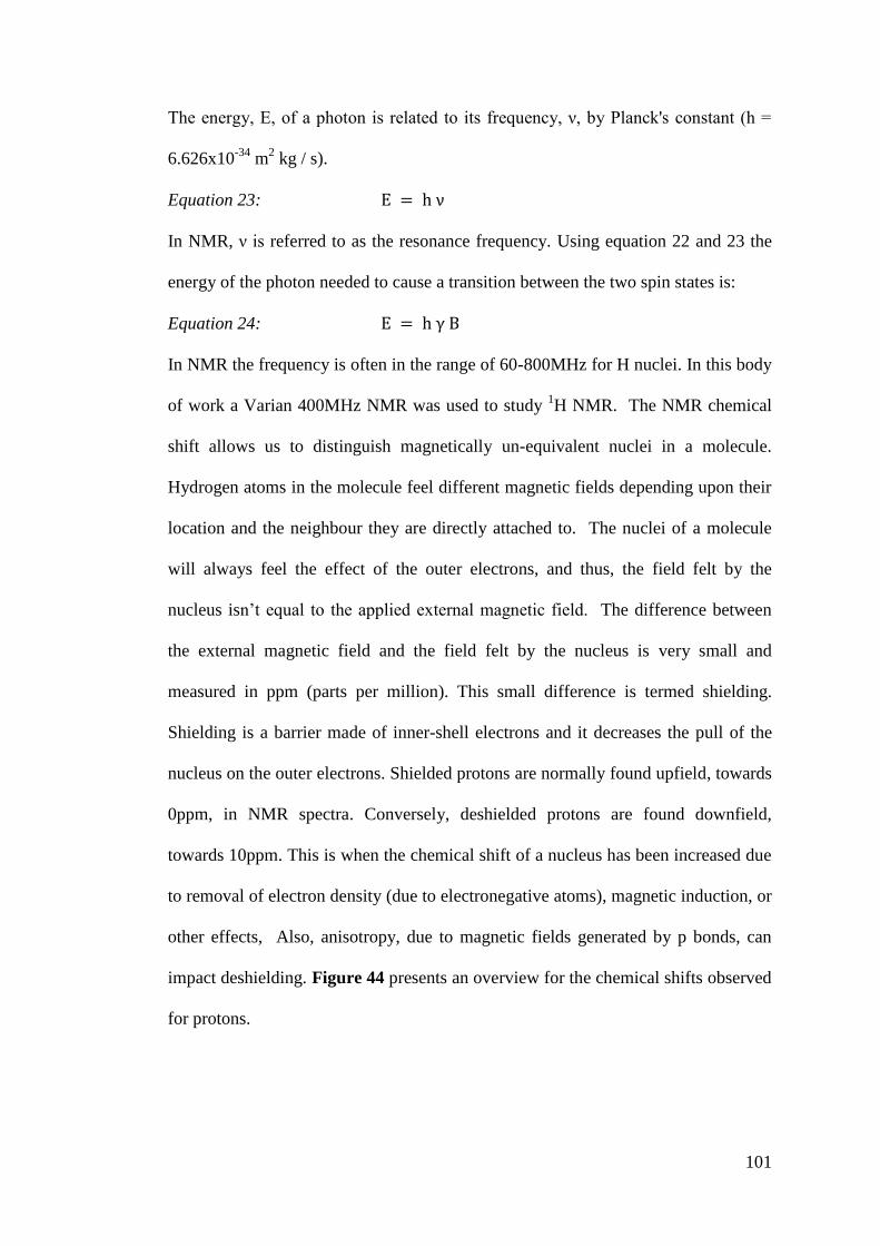
101
The energy, E, of a photon is related to its frequency, ν, by Planck's constant (h =
6.626x10⁻³⁴
m2 kg / s).
Equation 23:
In NMR, ν is referred to as the resonance frequency. Using equation 22 and 23 the
energy of the photon needed to cause a transition between the two spin states is:
Equation 24:
In NMR the frequency is often in the range of 60-800MHz for H nuclei. In this body
of work a Varian 400MHz NMR was used to study 1H NMR. The NMR chemical
shift allows us to distinguish magnetically un-equivalent nuclei in a molecule.
Hydrogen atoms in the molecule feel different magnetic fields depending upon their
location and the neighbour they are directly attached to. The nuclei of a molecule
will always feel the effect of the outer electrons, and thus, the field felt by the
nucleus isn’t equal to the applied external magnetic field. The difference between
the external magnetic field and the field felt by the nucleus is very small and
measured in ppm (parts per million). This small difference is termed shielding.
Shielding is a barrier made of inner-shell electrons and it decreases the pull of the
nucleus on the outer electrons. Shielded protons are normally found upfield, towards
0ppm, in NMR spectra. Conversely, deshielded protons are found downfield,
towards 10ppm. This is when the chemical shift of a nucleus has been increased due
to removal of electron density (due to electronegative atoms), magnetic induction, or
other effects, Also, anisotropy, due to magnetic fields generated by p bonds, can
impact deshielding. Figure 44 presents an overview for the chemical shifts observed
for protons.
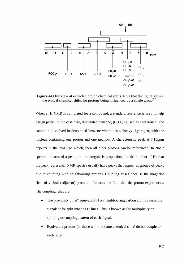
102
Figure 44 Overview of expected proton chemical shifts. Note that the figure shows
the typical chemical shifts for protons being influenced by a single group283
.
When a 1H NMR is completed for a compound, a standard reference is used to help
assign peaks. In the case here, dueterated benzene, (C6D6) is used as a reference. The
sample is dissolved in deuterated benzene which has a ‘heavy’ hydrogen, with the
nucleus containing one proton and one neutron. A characteristic peak at 7.15ppm
appears in the NMR to which, then all other protons can be referenced. In NMR
spectra the area of a peak, i.e. its integral, is proportional to the number of Hs that
the peak represents. NMR spectra usually have peaks that appear as groups of peaks
due to coupling with neighbouring protons. Coupling arises because the magnetic
field of vicinal (adjacent) protons influences the field that the proton experiences.
The coupling rules are:
The proximity of "n" equivalent H on neighbouring carbon atoms causes the
signals to be split into "n+1" lines. This is known as the multiplicity or
splitting or coupling pattern of each signal.
Equivalent protons (or those with the same chemical shift) do not couple to
each other.
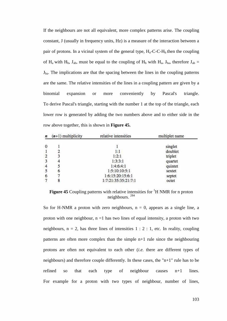
103
If the neighbours are not all equivalent, more complex patterns arise. The coupling
constant, J (usually in frequency units, Hz) is a measure of the interaction between a
pair of protons. In a vicinal system of the general type, Ha-C-C-Hb then the coupling
of Ha with Hb, Jab, must be equal to the coupling of Hb with Ha, Jba, therefore Jab =
Jba. The implications are that the spacing between the lines in the coupling patterns
are the same. The relative intensities of the lines in a coupling pattern are given by a
binomial expansion or more conveniently by Pascal's triangle.
To derive Pascal's triangle, starting with the number 1 at the top of the triangle, each
lower row is generated by adding the two numbers above and to either side in the
row above together, this is shown in Figure 45.
Figure 45 Coupling patterns with relative intensities for 1H NMR for n proton
neighbours. 284
So for H-NMR a proton with zero neighbours, n = 0, appears as a single line, a
proton with one neighbour, n =1 has two lines of equal intensity, a proton with two
neighbours, n = 2, has three lines of intensities 1 : 2 : 1, etc. In reality, coupling
patterns are often more complex than the simple n+1 rule since the neighbouring
protons are often not equivalent to each other (i.e. there are different types of
neighbours) and therefore couple differently. In these cases, the "n+1" rule has to be
refined so that each type of neighbour causes n+1 lines.
For example for a proton with two types of neighbour, number of lines,
104
L=(n1+1)(n2+1). However, in many cases the lines overlap with each other and the
result is further distortion from the "ideal" pattern. Coupling patterns involving
aromatic or alkene protons are often complex.
3.1.2 Inductively Coupled Plasma (ICP)
ICP is a method of detecting trace impurities within chemical samples. A plasma is a
highly energized ‘cloud’ of gaseous ions and their electrons. An ICP can be
generated by coupling the energy of a radio frequency generator into a suitable gas,
usually argon. This coupling is achieved by generating a magnetic field by passing a
high frequency electric current through a cooled coil. This inductor generates a
rapidly oscillating magnetic field orientated in the vertical plain of the coil. The
plasma is initiated by seeding the argon gas with electrons via such means as a
spark. The electrons are then accelerated in the magnetic field, rapidly reaching the
ionization energy. This process combined with collision of argon atoms make the
plasma self-sustaining. As the electrons and ions are under the influence of the
magnetic field, the flow is directed. The high temperature of the plasma (upto
10,000K) ensures complete atomization, ensuring elemental analysis can be
determined. There are two types of ICP analysis that were used within this body of
work: ICP-Mass Spectrometry (ICP-MS) is based on the production, sampling and
mass filtering of positive ions. This is shown schematically in Figure 46.
Figure 46 Schematic for ICP-MS. 285
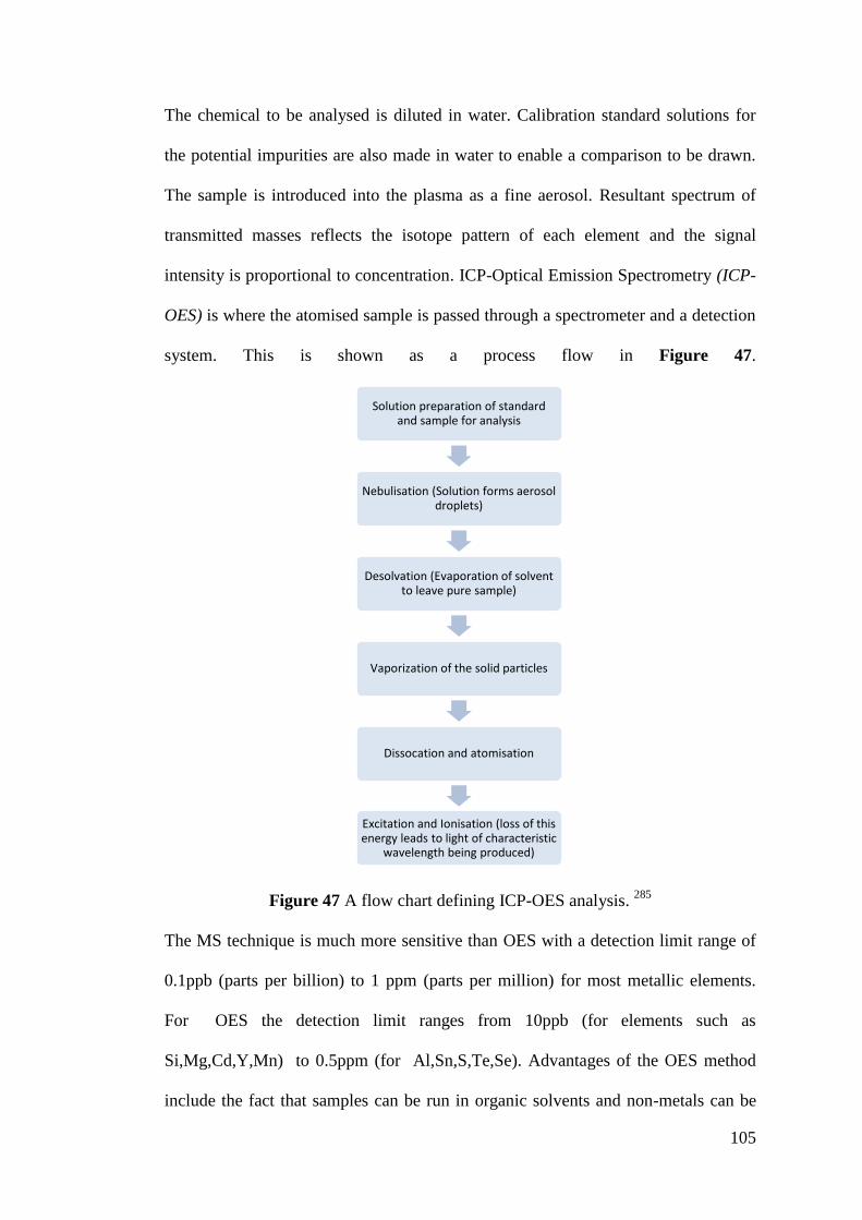
105
The chemical to be analysed is diluted in water. Calibration standard solutions for
the potential impurities are also made in water to enable a comparison to be drawn.
The sample is introduced into the plasma as a fine aerosol. Resultant spectrum of
transmitted masses reflects the isotope pattern of each element and the signal
intensity is proportional to concentration. ICP-Optical Emission Spectrometry (ICP-
OES) is where the atomised sample is passed through a spectrometer and a detection
system. This is shown as a process flow in Figure 47.
Figure 47 A flow chart defining ICP-OES analysis. 285
The MS technique is much more sensitive than OES with a detection limit range of
0.1ppb (parts per billion) to 1 ppm (parts per million) for most metallic elements.
For OES the detection limit ranges from 10ppb (for elements such as
Si,Mg,Cd,Y,Mn) to 0.5ppm (for Al,Sn,S,Te,Se). Advantages of the OES method
include the fact that samples can be run in organic solvents and non-metals can be
Solution preparation of standard and sample for analysis
Nebulisation (Solution forms aerosol droplets)
Desolvation (Evaporation of solvent to leave pure sample)
Vaporization of the solid particles
Dissocation and atomisation
Excitation and Ionisation (loss of this energy leads to light of characteristic
wavelength being produced)
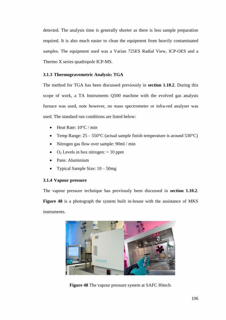
106
detected. The analysis time is generally shorter as there is less sample preparation
required. It is also much easier to clean the equipment from heavily contaminated
samples. The equipment used was a Varian 725ES Radial View, ICP-OES and a
Thermo X series quadropole ICP-MS.
3.1.3 Thermogravemetric Analysis: TGA
The method for TGA has been discussed previously in section 1.10.2. During this
scope of work, a TA Instruments Q500 machine with the evolved gas analysis
furnace was used, note however, no mass spectrometer or infra-red analyser was
used. The standard run conditions are listed below:
Heat Rate: 10°C / min
Temp Range: 25 – 550°C (actual sample finish temperature is around 530°C)
Nitrogen gas flow over sample: 90ml / min
O2 Levels in box nitrogen: < 10 ppm
Pans: Aluminium
Typical Sample Size: 10 – 50mg
3.1.4 Vapour pressure
The vapour pressure technique has previously been discussed in section 1.10.2.
Figure 48 is a photograph the system built in-house with the assistance of MKS
instruments.
Figure 48 The vapour pressure system at SAFC Hitech.
107
All details are provided from an SAFC Hitech publication. 286
The key sections of
the system are located inside an oven to ensure uniform heating of all parts is
achieved to prevent condensation issues. The sample chamber is attached to a
vacuum manifold equipped with a BaratronTM
pressure measurement gauge and a
second BaratronTM
is located outside the oven along with the computer connections
etc. The construction material is stainless steel with high integrity joints throughout.
The sample for study is placed in the test chamber and vacuum applied to remove
inert atmosphere process gas. It should be noted that out gassing from the sample is
of critical importance when investigating vapour pressure measurement, especially
in the less than 1Torr range. The trial temperature is established and pressure
readings taken over several minutes to establish an accurate, stable value. Once three
steady readings have been recorded the temperature is raised and allowed to
equilibrate before repeating the process to get a second point. The temperature is
raised again to get a third and so on until a maximum temperature is reached.
3.1.5 Crystal Structures
Crystal structure data was collected by Dr. Steiner and Dr. Basca at the University of
Liverpool using a Bruker D8 diffractometer with an APEX CCD detector, and 1.5
kW graphite monochromatic Mo radiation. Specific details for each structure are
given within the experimental section of each results chapter.
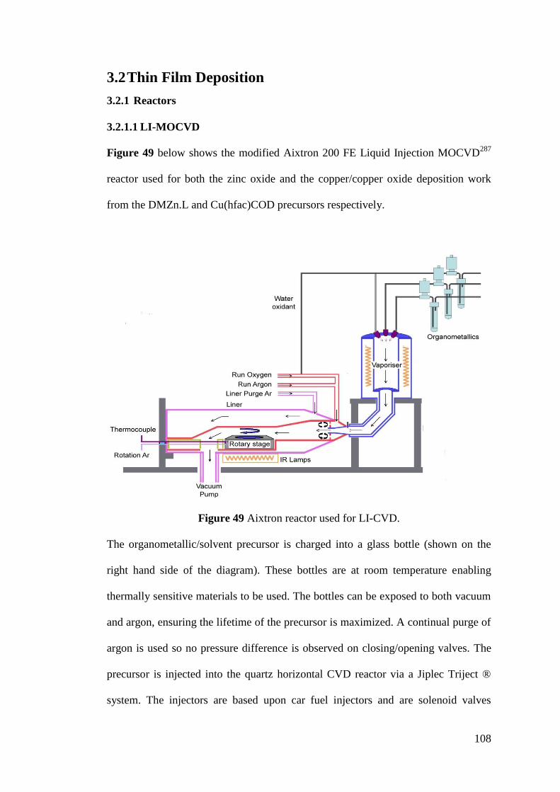
108
3.2 Thin Film Deposition
3.2.1 Reactors
3.2.1.1 LI-MOCVD
Figure 49 below shows the modified Aixtron 200 FE Liquid Injection MOCVD287
reactor used for both the zinc oxide and the copper/copper oxide deposition work
from the DMZn.L and Cu(hfac)COD precursors respectively.
Figure 49 Aixtron reactor used for LI-CVD.
The organometallic/solvent precursor is charged into a glass bottle (shown on the
right hand side of the diagram). These bottles are at room temperature enabling
thermally sensitive materials to be used. The bottles can be exposed to both vacuum
and argon, ensuring the lifetime of the precursor is maximized. A continual purge of
argon is used so no pressure difference is observed on closing/opening valves. The
precursor is injected into the quartz horizontal CVD reactor via a Jiplec Triject ®
system. The injectors are based upon car fuel injectors and are solenoid valves
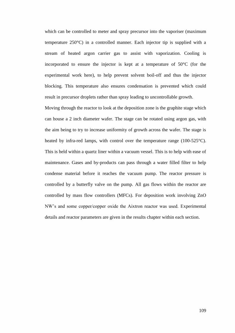
109
which can be controlled to meter and spray precursor into the vaporiser (maximum
temperature 250°C) in a controlled manner. Each injector tip is supplied with a
stream of heated argon carrier gas to assist with vaporization. Cooling is
incorporated to ensure the injector is kept at a temperature of 50°C (for the
experimental work here), to help prevent solvent boil-off and thus the injector
blocking. This temperature also ensures condensation is prevented which could
result in precursor droplets rather than spray leading to uncontrollable growth.
Moving through the reactor to look at the deposition zone is the graphite stage which
can house a 2 inch diameter wafer. The stage can be rotated using argon gas, with
the aim being to try to increase uniformity of growth across the wafer. The stage is
heated by infra-red lamps, with control over the temperature range (100-525°C).
This is held within a quartz liner within a vacuum vessel. This is to help with ease of
maintenance. Gases and by-products can pass through a water filled filter to help
condense material before it reaches the vacuum pump. The reactor pressure is
controlled by a butterfly valve on the pump. All gas flows within the reactor are
controlled by mass flow controllers (MFCs). For deposition work involving ZnO
NW’s and some copper/copper oxide the Aixtron reactor was used. Experimental
details and reactor parameters are given in the results chapter within each section.
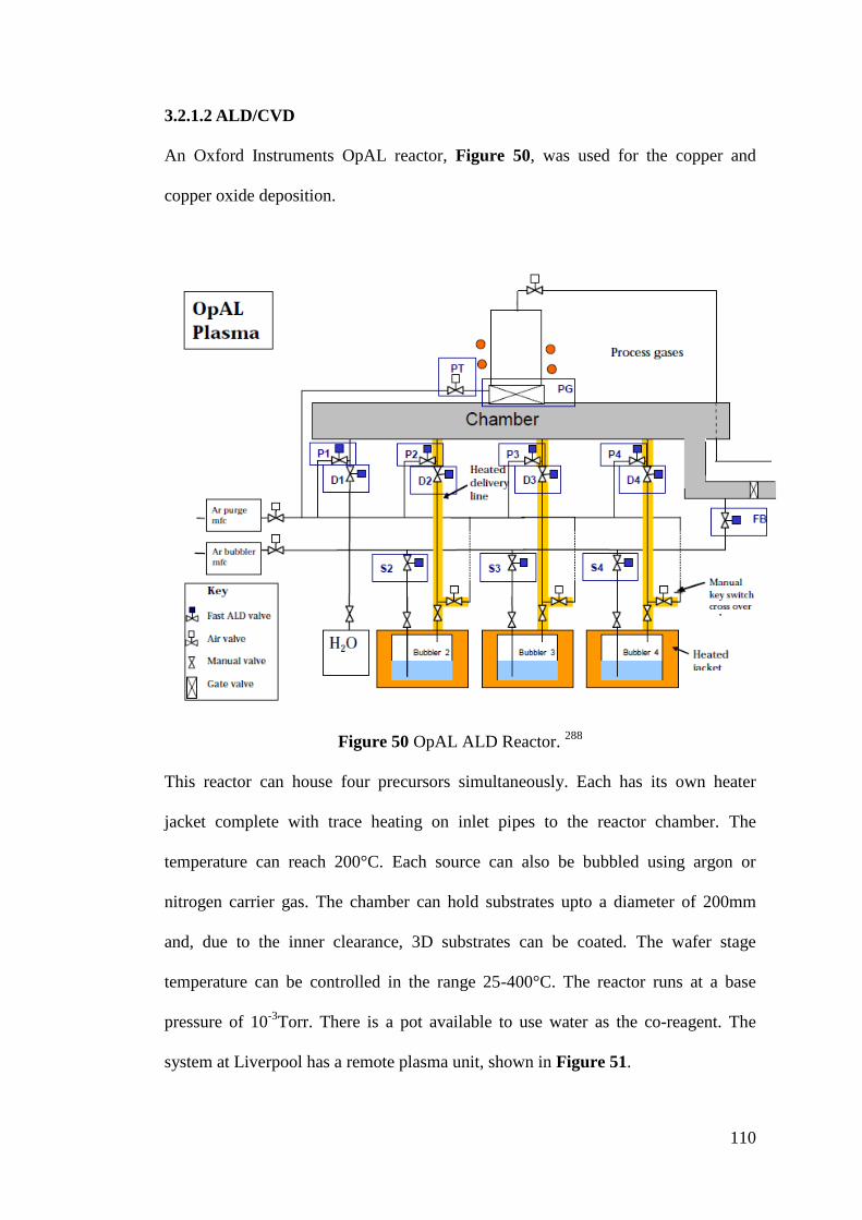
110
3.2.1.2 ALD/CVD
An Oxford Instruments OpAL reactor, Figure 50, was used for the copper and
copper oxide deposition.
Figure 50 OpAL ALD Reactor. 288
This reactor can house four precursors simultaneously. Each has its own heater
jacket complete with trace heating on inlet pipes to the reactor chamber. The
temperature can reach 200°C. Each source can also be bubbled using argon or
nitrogen carrier gas. The chamber can hold substrates upto a diameter of 200mm
and, due to the inner clearance, 3D substrates can be coated. The wafer stage
temperature can be controlled in the range 25-400°C. The reactor runs at a base
pressure of 10-3
Torr. There is a pot available to use water as the co-reagent. The
system at Liverpool has a remote plasma unit, shown in Figure 51.
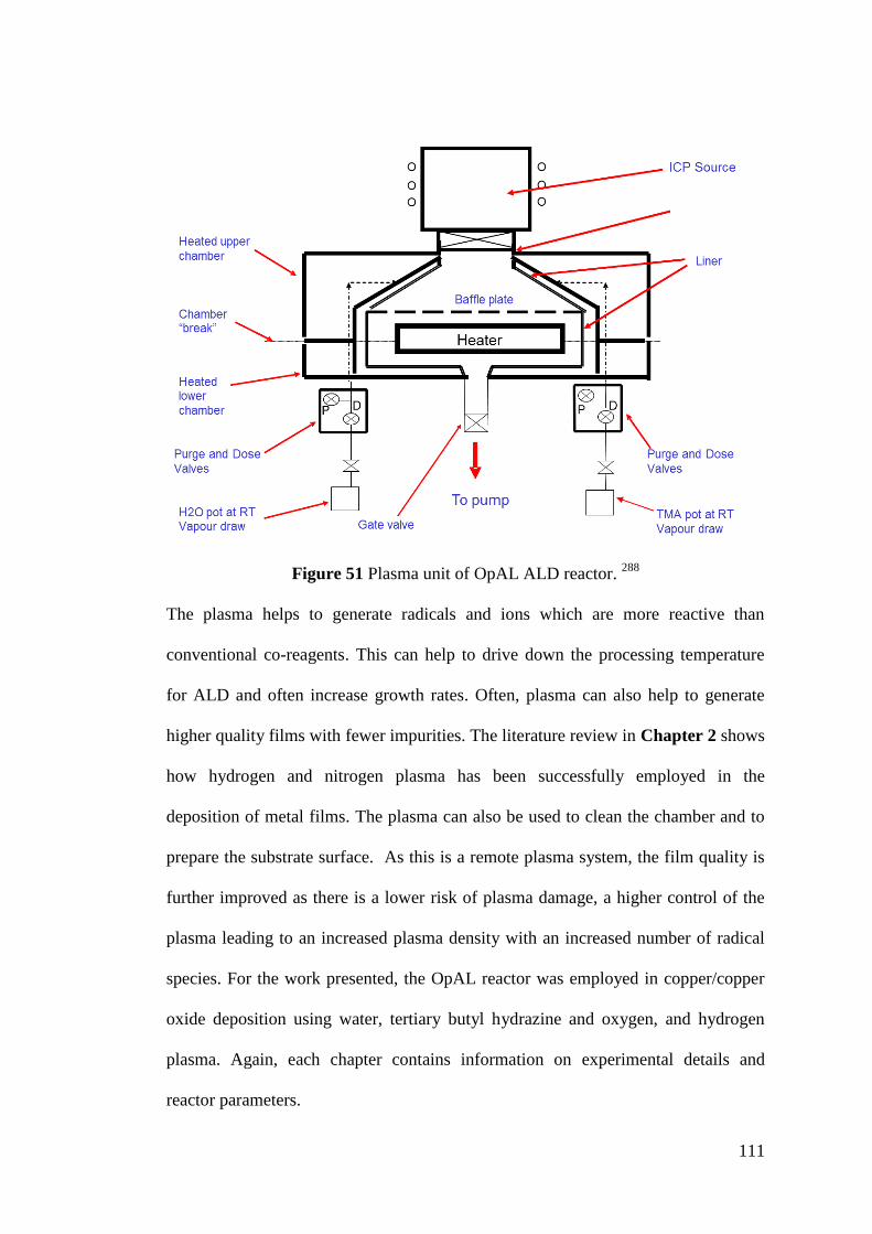
111
Figure 51 Plasma unit of OpAL ALD reactor. 288
The plasma helps to generate radicals and ions which are more reactive than
conventional co-reagents. This can help to drive down the processing temperature
for ALD and often increase growth rates. Often, plasma can also help to generate
higher quality films with fewer impurities. The literature review in Chapter 2 shows
how hydrogen and nitrogen plasma has been successfully employed in the
deposition of metal films. The plasma can also be used to clean the chamber and to
prepare the substrate surface. As this is a remote plasma system, the film quality is
further improved as there is a lower risk of plasma damage, a higher control of the
plasma leading to an increased plasma density with an increased number of radical
species. For the work presented, the OpAL reactor was employed in copper/copper
oxide deposition using water, tertiary butyl hydrazine and oxygen, and hydrogen
plasma. Again, each chapter contains information on experimental details and
reactor parameters.
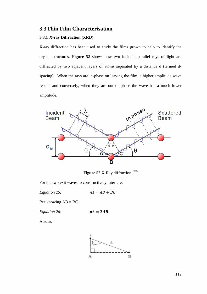
112
3.3 Thin Film Characterisation
3.3.1 X-ray Diffraction (XRD)
X-ray diffraction has been used to study the films grown to help to identify the
crystal structures. Figure 52 shows how two incident parallel rays of light are
diffracted by two adjacent layers of atoms separated by a distance d (termed d-
spacing). When the rays are in-phase on leaving the film, a higher amplitude wave
results and conversely, when they are out of phase the wave has a much lower
amplitude.
Figure 52 X-Ray diffraction. 289
For the two exit waves to constructively interfere:
Equation 25:
But knowing AB = BC
Equation 26:
Also as
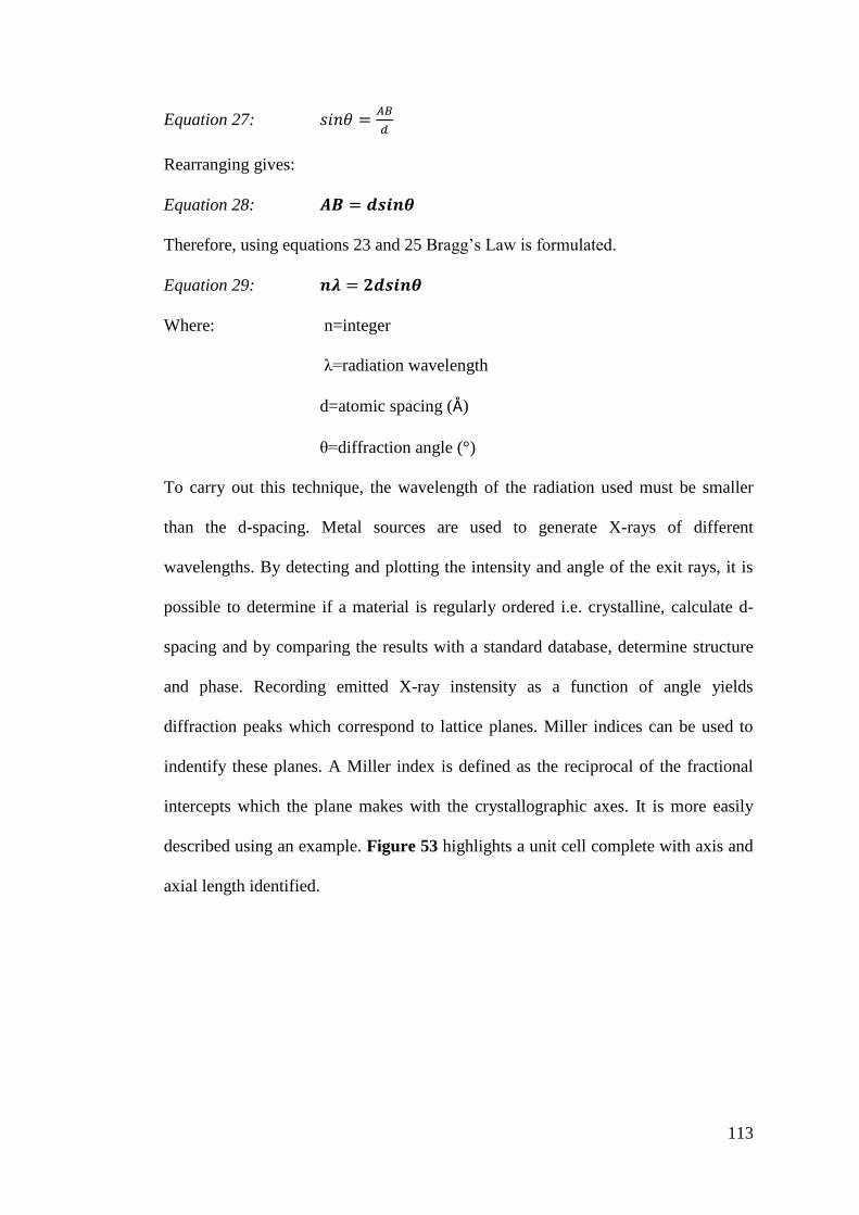
113
Equation 27:
Rearranging gives:
Equation 28:
Therefore, using equations 23 and 25 Bragg’s Law is formulated.
Equation 29:
Where: n=integer
λ=radiation wavelength
d=atomic spacing (Å)
θ=diffraction angle (°)
To carry out this technique, the wavelength of the radiation used must be smaller
than the d-spacing. Metal sources are used to generate X-rays of different
wavelengths. By detecting and plotting the intensity and angle of the exit rays, it is
possible to determine if a material is regularly ordered i.e. crystalline, calculate d-
spacing and by comparing the results with a standard database, determine structure
and phase. Recording emitted X-ray instensity as a function of angle yields
diffraction peaks which correspond to lattice planes. Miller indices can be used to
indentify these planes. A Miller index is defined as the reciprocal of the fractional
intercepts which the plane makes with the crystallographic axes. It is more easily
described using an example. Figure 53 highlights a unit cell complete with axis and
axial length identified.
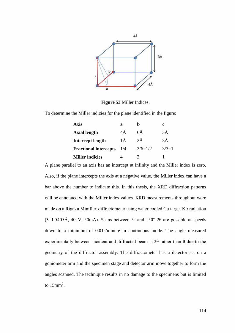
114
Figure 53 Miller Indices.
To determine the Miller indicies for the plane identified in the figure:
Axis a b c
Axial length 4Å 6Å 3Å
Intercept length 1Å 3Å 3Å
Fractional intercepts 1/4 3/6=1/2 3/3=1
Miller indicies 4 2 1
A plane parallel to an axis has an intercept at infinity and the Miller index is zero.
Also, if the plane intercepts the axis at a negative value, the Miller index can have a
bar above the number to indicate this. In this thesis, the XRD diffraction patterns
will be annotated with the Miller index values. XRD measurements throughout were
made on a Rigaku Miniflex diffractometer using water cooled Cu target Kα radiation
(λ=1.5405Å, 40kV, 50mA). Scans between 5° and 150° 2θ are possible at speeds
down to a minimum of 0.01°/minute in continuous mode. The angle measured
experimentally between incident and diffracted beam is 2θ rather than θ due to the
geometry of the diffractor assembly. The diffractometer has a detector set on a
goniometer arm and the specimen stage and detector arm move together to form the
angles scanned. The technique results in no damage to the specimens but is limited
to 15mm2.
115
3.3.2 Raman
Raman spectroscopy is a non-destructive technique which can provide information
on the physical structure and phase of a material as a result of the inelastic scattering
of light. When a photon of visible light that is too low in energy to excite an
electronic transition interacts with a molecule, it can be scattered and therefore
retains its incident energy. Rayleigh scattering arises from transitions that start and
finish from the same vibrational energy level. Stokes Raman scattering arrives from
transitions which start at the ground state vibrational energy level and finish as
higher vibrational energy level, the photon has lost energy to the molecule. Anti-
stokes Raman scattering involve a transition from a higher to a lower vibrational
energy level, the photon has gained energy. Since molecular energy levels are
quantised this produces discrete lines from which we can gain information on the
molecule itself. This is shown schematically in Figure 54.
Figure 54 Raman scattering modes. 290
116
The Raman shift depends on the energy spacing of the molecules’ modes. However
not all modes are “Raman active” i.e. not all appear in Raman spectra. For a mode to
be Raman active it must involve a change in the polarisability, α of the molecule.
This can be caused by vibrational, rotational and electronic modes. Theory can
regard the scattering molecule as a collection of atoms undergoing simple harmonic
vibrations and takes no account of quantisation of the vibrational energy. If the
molecule is placed in an electric field, its electrons are displaced relative to its nuclei
and therefore it develops an electric dipole moment. The induced dipole moment µi
is proportional to the field strength ԑ:
Equation 30:
A fluctuating electric field produces a fluctuating dipole moment of the same
frequency. The electromagnetic radiation is responsible for the generation of the
electric field and this can be expressed as:
Equation 31:
Where: is the equilibrium field strength
is the angular frequency of the radiation.
In this study, Raman experiments were conducted by Dr Peter King using a
Renishaw Compact System 100. The apparatus consists of an optical microscope
and several laser sources, from which the beam is focused through a series of optics.
The laser focuses on a specimen surface at the same point the visible light comes
into focus. A choice of lasers are available, with a 325nm HeCd ultra-violet (UV)
and an Argon ion (Ar+) laser at 514.53nm most useful for thin-film analysis. The
spectrometer sweeps a wavenumber range with the time spent and number of
acquisitions per wavenumber band set before operation. Experimental parameters
are given within the experimental details section of each chapter.
117
3.3.3 Scanning Electron Microscopy (SEM)
The scanning electron microscope (SEM) uses a focused beam of high-energy
electrons to generate a variety of signals at the surface of solid specimens. The
signals that derive from electron-sample interactions reveal information about the
sample including external morphology, chemical composition, and crystalline
structure and orientation of materials making up the sample.
A beam of electrons is produced at the top of the microscope by an electron gun.
The electron beam follows a vertical path through the microscope, which is held
within a vacuum. The beam travels through electromagnetic fields and lenses, which
focus the beam down toward the sample. Accelerated electrons in an SEM carry
significant amounts of kinetic energy and this energy is dissipated as a variety of
signals produced by electron-sample interactions when the incident electrons are
decelerated in the solid sample. These signals include secondary electrons (that
produce SEM images), backscattered electrons, (used to determine crystal structures
and orientations), and photons (characteristic X-rays that are used for elemental
analysis). Secondary electrons and backscattered electrons are commonly used for
imaging samples: secondary electrons are most valuable for showing morphology
and topography on samples and backscattered electrons are most valuable for
illustrating contrasts in composition.
For this research, SEM imaging was employed to reveal surface morphology and
was conducted by Dr. Simon Romani, Dr Kerry Abrams, Dr Tobias Heil or Dr Karl
Dawson. For the copper metal and oxide analysis a Jeol 7001F SEM and a FEI
Helios 600i FIB SEM was used. For the zinc oxide analysis imaging was conducted
by both Dr Matt Werner and myself with a field emission Hitachi S-2460N SEM, at
an acceleration voltage of 20 kV. For the later SEM, wafer sections were divided
118
and mounted with conductive tape onto the goniometer stage of the microscope,
enabling the samples to be examined in all directions.
3.3.4 Energy Dispersive X-ray (EDX)
Elemental analysis is possible due to the unique characteristic X-ray emissions that
occur from the inelastic interaction of the electron beam in an SEM with individual
atoms. This phenomenon arises when a high-energy beam electron penetrates and
interacts with the inner shell electrons of the atom. During this interaction, if
sufficient energy is transferred to one of the core electrons, the electron is ejected
and the atom is left in an excited states. In order to return to its ground state, the hole
is filled by one of the outer shell electrons and to ensure the energy is conserved, an
x-ray is emitted. The energy of this emission is characteristic of the difference in
energy of the two electron shells involved and thus is unique to the atom or element.
In thin film analysis, the peaks for all elements present, including the substrate, will
be observed. EDX does have limitations. It is more sensitive to higher atomic
number elements than lower atomic number elements e.g. carbon and oxygen.
3.3.5 Transmission Electron Microscopy (TEM)
TEM was used to gain information on film morphology and crystalline phase, as
well as film thickness. This technique uses transmitted electrons which pass through
the sample, limiting specimen thicknesses to a few hundreds of nanometres. For
TEM analysis of this work, TEM grids were placed in the reactor during
depositions. Although this does not fully replicate the film deposited on the various
substrates, it negates the need for time intensive sample preparation. TEM beam
energy is much higher (50-300keV) than SEM since the incident electrons require
higher energy to pass through the sample. Elastic scattering of electrons in
crystalline materials give rise to characteristic diffraction patterns, whilst both elastic
119
and inelastic effects are used to generate TEM images in either bright or dark field.
When an image is formed using the central spot from the direct beam, a bright field
image is seen. Low atomic number elements scatter electrons through a smaller
angle, so these appear light in an image; whereas, higher atomic number elements
scatter electrons at higher angles and so appear darker. By contrast, when some or
all of the scattered electrons are used we generate a dark field image. This examines
higher angles of electron scattering, where low atomic number elements appear dark,
and higher atomic number elements appear light. To choose which electrons form
the image, an aperture is inserted thus blocking out most of the diffraction pattern
except that which is visible through the aperture, this is often dependent upon
sample composition.
For this research, TEM imaging was conducted by Dr. Simon Romani, Dr Kerry
Abrams, Dr Tobias Heil or Dr Karl Dawson. The TEM used was a Jeol 2100F TEM.
3.3.6 Energy Electron Loss Spectroscopy (EELs)
EELs measures any changes in energy when electrons pass through a sample. Elastic
scattering occurs when the electron interacts with atomic nuclei. As the nucleus is
highly charged, the electric field felt by the electron is large, resulting in high angles
of scattering. Inelastic scattering occurs when the incident electrons interact with the
atomic electrons in the sample. Sometimes, this can promote an inner shell electron
to a higher empty orbital, which, at some time will decay back down to its ground
state and emit the excess energy as e.g. an xray or to another atomic electron (Auger
electron). If the incident electron collides with an outer shell electron, there may be
enough energy to emit the outer electron, resulting in the release of a secondary
electron.
120
The secondary processes of electron and photon emission from a specimen can be
studied in detail by appropriate spectroscopies. In EELs the primary process of
electron excitation, which results in the fast electron losing a characteristic amount
of energy is studied. The transmitted electron beam is directed into a high-resolution
electron spectrometer that separates the electrons according to their kinetic energy
and produces an electron energy-loss spectrum showing the number of electrons
(scattered intensity) as a function of their decrease in kinetic energy. An EELs
spectra often has a 'zero loss' peak in which the electrons pass straight through the
sample with no change in energy. Inner shell excitations are observed as sharp
edges, with the sharp rise occuring at the ionization threshold. This is where the
energy-loss is approximately the binding energy of the corresponding atomic shell.
Since inner-shell binding energies depend on the atomic number of the scattering
atom, the ionization edges present in an energy-loss spectrum reveal which elements
are present within the specimen. If the energy-loss spectrum is recorded from a thin
sample, each spectral feature corresponds to a different excitation process. In thicker
samples, there is a substantial probability that a transmitted electron will be
inelastically scattered more than once, giving a total energy loss equal to the sum of
the individual losses.
For the work presented within this thesis, EELs spectra were recorded by Dr Tobias
Heil on copper samples of less than 80nm. The IMFP of copper for the used electron
energy of 200kV is 96nm.291
3.3.7 Auger Electron Spectroscopy (AES)
Auger Electron Spectroscopy (AES) is an analytical technique that uses a primary
electron beam to probe the surface of a solid material. The basic Auger process starts
with removal of an inner shell atomic electron to form a vacancy. Several processes
121
are capable of producing the vacancy, but bombardment with an electron beam is the
most common. The inner shell vacancy is filled by a second atomic electron from a
higher shell. Energy must be simultaneously released. A third electron, the Auger
electron, escapes carrying the excess energy in a radiationless process. The process
of an excited ion decaying into a doubly charged ion by ejection of an electron is
called the Auger process. As described, the Auger process requires three electrons,
thus we cannot detect H or He but can detect all other elements from Li and up.
Secondary electrons that are emitted as a result of the Auger process are analysed
and their kinetic energy is determined. The identity and quantity of the elements are
determined from the kinetic energy and intensity of the Auger peaks. The nature of
the Auger surface analysis process is such that Auger electrons can only escape from
the outer 5-50 Å of a solid surface at their characteristic energy. This effect makes
AES an extremely surface sensitive technique. A finely focused electron beam can
be scanned to create secondary electron and Auger images, or the beam can be
positioned to perform microanalysis of specific sample features.
AES was carried out as part of the previous work by Black196
. AES data were
excited using the 325nm wavelength from a He-Cd laser. The atomic compositions
quoted in Chapter 4 are from the subsurface of the nanowire structures, and were
obtained by combining AES with sequential argon ion bombardment until
comparable compositions were obtained for consecutive data points. Compositions
were based on a ZnO powder reference.
3.3.8 Photoluminescence (PL) Spectroscopy
Photoluminescence (PL) spectroscopy is a contactless, nondestructive method to
probe the electronic structure of materials. Photoluminescence occurs when an
external source of energy, in the form of electromagnetic radiation, is absorbed by
122
an atom. If a light particle (photon) has an energy greater than the band gap energy,
then it can be absorbed and thereby raise an electron from the valence band up to the
conduction band across the forbidden energy gap. In this process of photoexcitation,
the electron generally has excess energy which it loses before coming to rest at the
lowest energy in the conduction band. At this point the electron eventually falls back
down to the valence band. As it falls down, the energy it loses is converted back into
a luminescent photon which is emitted from the material. Thus the energy of the
emitted photon is a direct measure of the band gap energy. The PL spectrum often
reveals spectral peaks associated with impurities contained within the host material.
The high sensitivity of this technique provides the potential to identify extremely
low concentrations of intentional and unintentional impurities that can strongly
affect material quality and device performance. The quantity of PL emitted from a
material is directly related to the relative amount of radiative and nonradiative
recombination rates. Non-radiative rates are typically associated with impurities and
thus, this technique can qualitatively monitor changes in material quality as a
function of growth and processing conditions. A PL spectrum was collected as part
of the work of Kate Black on ZnO NWs. PL data were acquired using a Jobin-Yvon
LabRam HR consisting of a confocal microscope coupled to a single grating
spectrometer equipped with a notch filter and a CCD camera detector. All of the
spectra were recorded in a backscattering geometry.
3.3.9 Ellipsometery
Ellipsometry measures a change in polarization as light reflects or transmits from a
material structure. The polarization change is represented as an amplitude ratio, Ψ,
and the phase difference, Δ. The measured response depends on optical properties
and thickness of individual materials. Thus, ellipsometry is primarily used to
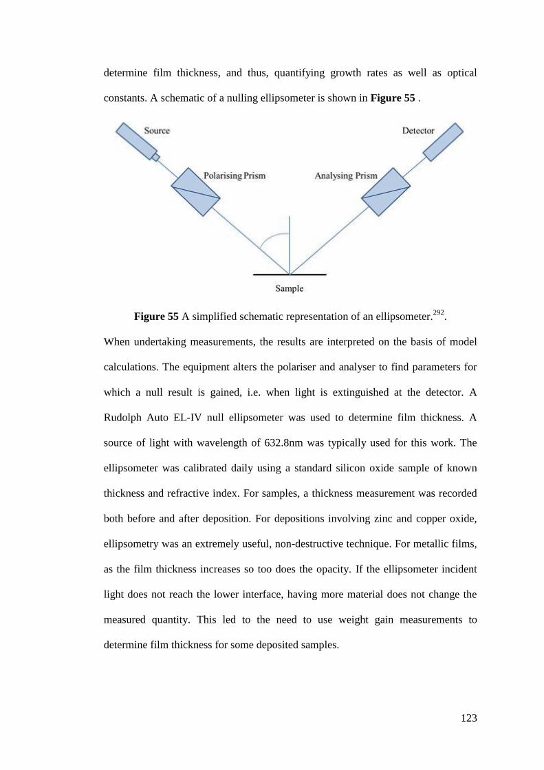
123
determine film thickness, and thus, quantifying growth rates as well as optical
constants. A schematic of a nulling ellipsometer is shown in Figure 55 .
Figure 55 A simplified schematic representation of an ellipsometer.292
.
When undertaking measurements, the results are interpreted on the basis of model
calculations. The equipment alters the polariser and analyser to find parameters for
which a null result is gained, i.e. when light is extinguished at the detector. A
Rudolph Auto EL-IV null ellipsometer was used to determine film thickness. A
source of light with wavelength of 632.8nm was typically used for this work. The
ellipsometer was calibrated daily using a standard silicon oxide sample of known
thickness and refractive index. For samples, a thickness measurement was recorded
both before and after deposition. For depositions involving zinc and copper oxide,
ellipsometry was an extremely useful, non-destructive technique. For metallic films,
as the film thickness increases so too does the opacity. If the ellipsometer incident
light does not reach the lower interface, having more material does not change the
measured quantity. This led to the need to use weight gain measurements to
determine film thickness for some deposited samples.

124
3.3.10 Film thickness from weight gain measurements
The average film thickness can be determined by measuring the weight gain of a
wafer during coating and inputting this into equation 32
Equation 32:
Where: is the average film thickness (nm)
is the weight gain of the deposited sample (g)
is the area of the substrate (cm2)
ρ is the film density (taken from literature) (g/cm-3
).
Potential errors for this technique arise from
weighing-error of the weigh scale is ±0.001g.
area-due to the range of substrates used for this work, the area and shape of
such substrates varied dramatically.
film composition and density-deposited samples may vary from those
reported in the literature due to reactor conditions and parameters. These
sources of variation are not always possible to quantify accurately.
Within the experimental sections, the method chosen for film thickness analysis will
be justified and described, and the possible errors accounted for.
3.3.11 Four point probe
A four point probe is a simple apparatus for measuring the resistivity of
semiconductor samples. By passing a current through two outer probes and
measuring the voltage through the inner probes, the substrate resistivity can be
determined. Electrical resistivity measurements were made with a four-point probe
system comprising a Lucas Signatone Corp SP4 Four Point Probe Head and a
Keithley Series 2400 SourcemeterVR .
125
Chapter 4 Zinc Results and Discussion
4.1 Overview
The overall thesis aim, given in section 1.6, can be further cascaded for zinc
precursor development and subseqsuent zinc oxide deposition studies. The
objectives included:
the development of a commercially viable precursor for the MOCVD of ZnO
nanostructures with full characterisation
to gain an understanding of the reaction mechanism in the MOCVD process
and how the deposition mechanism is altered by e.g. temperature, pressure,
precursor, and co-reactant
full analysis of the deposited ZnO
The research carried out on dialkylzinc and dialyklzinc adducts and the use of them
within MOCVD has proven vital to the developments within its field. The following
references are the peer reviewed papers published during the time-span of this
work.102, 106, 293, 294
This chapter details work from these publications carried out by
K. Black and S. Ashraf, along with my personal input of precursor development and
characterisation and some deposition studies. From precursor synthesis and
charactetersation, to zinc oxide deposition and final film analysis, all data is
included here for to help draw comparisons and conclusions.
4.2 Dialkylzinc Precursor Characterisation
4.2.1 Dialkylzinc Crystal Structures
Although R2Zn (R=Me, Et) compounds have been used extensively in both chemical
synthesis and thin film deposition, the solid-state structure of these species have
remained elusive. Within the scope of the work undertaken for this body of research,
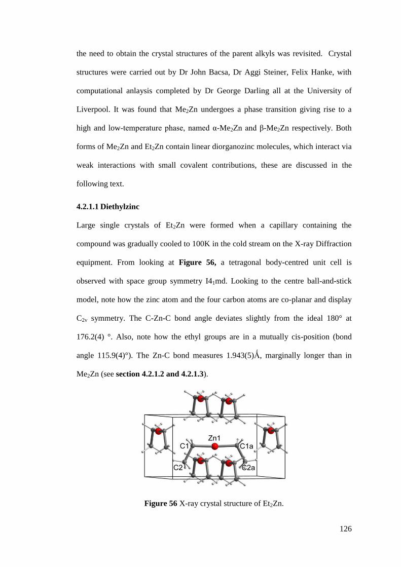
126
the need to obtain the crystal structures of the parent alkyls was revisited. Crystal
structures were carried out by Dr John Bacsa, Dr Aggi Steiner, Felix Hanke, with
computational anlaysis completed by Dr George Darling all at the University of
Liverpool. It was found that Me2Zn undergoes a phase transition giving rise to a
high and low-temperature phase, named α-Me2Zn and β-Me2Zn respectively. Both
forms of Me2Zn and Et2Zn contain linear diorganozinc molecules, which interact via
weak interactions with small covalent contributions, these are discussed in the
following text.
4.2.1.1 Diethylzinc
Large single crystals of Et2Zn were formed when a capillary containing the
compound was gradually cooled to 100K in the cold stream on the X-ray Diffraction
equipment. From looking at Figure 56, a tetragonal body-centred unit cell is
observed with space group symmetry I41md. Looking to the centre ball-and-stick
model, note how the zinc atom and the four carbon atoms are co-planar and display
C2v symmetry. The C-Zn-C bond angle deviates slightly from the ideal 180° at
176.2(4) °. Also, note how the ethyl groups are in a mutually cis-position (bond
angle 115.9(4)°). The Zn-C bond measures 1.943(5)Ǻ, marginally longer than in
Me2Zn (see section 4.2.1.2 and 4.2.1.3).
Figure 56 X-ray crystal structure of Et2Zn.
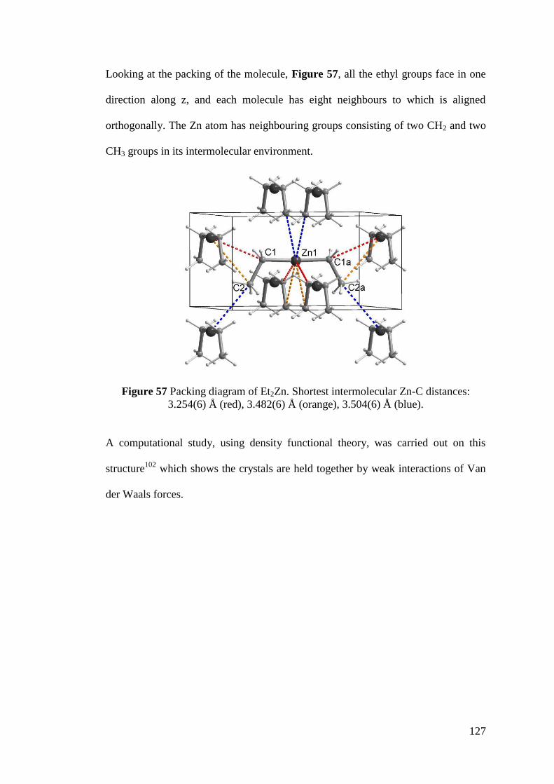
127
Looking at the packing of the molecule, Figure 57, all the ethyl groups face in one
direction along z, and each molecule has eight neighbours to which is aligned
orthogonally. The Zn atom has neighbouring groups consisting of two CH2 and two
CH3 groups in its intermolecular environment.
Figure 57 Packing diagram of Et2Zn. Shortest intermolecular Zn-C distances:
3.254(6) Å (red), 3.482(6) Å (orange), 3.504(6) Å (blue).
A computational study, using density functional theory, was carried out on this
structure102
which shows the crystals are held together by weak interactions of Van
der Waals forces.
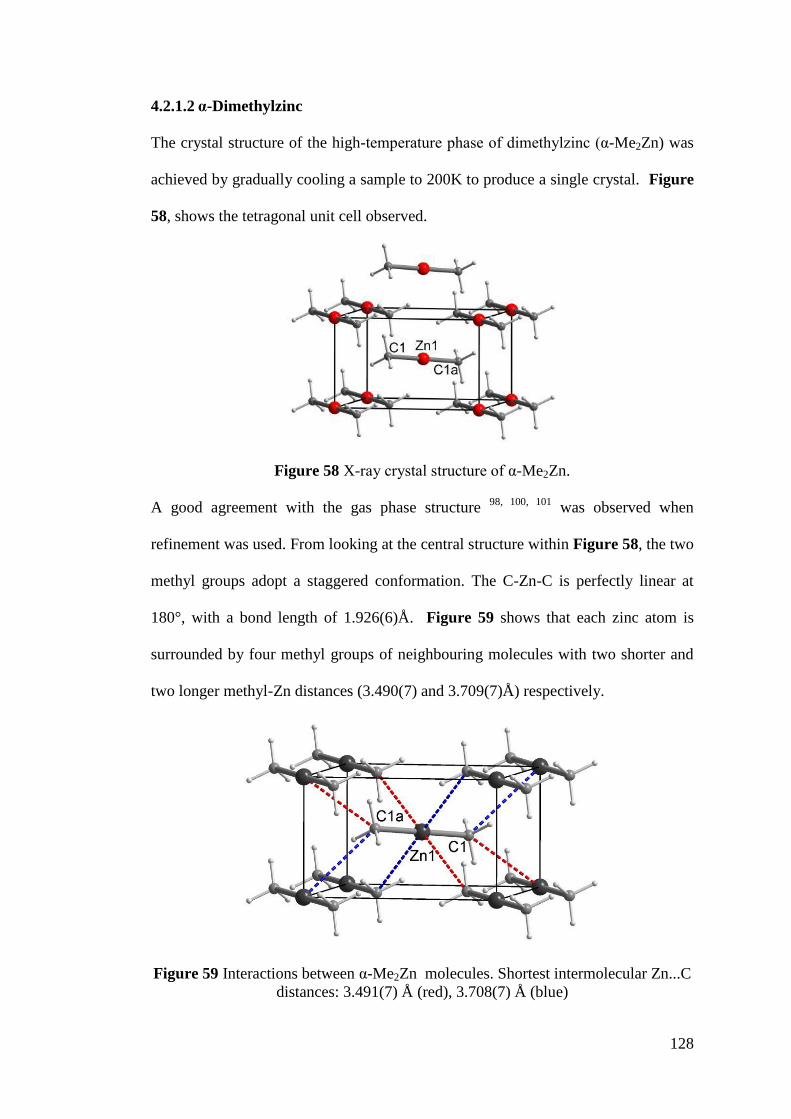
128
4.2.1.2 α-Dimethylzinc
The crystal structure of the high-temperature phase of dimethylzinc (α-Me2Zn) was
achieved by gradually cooling a sample to 200K to produce a single crystal. Figure
58, shows the tetragonal unit cell observed.
Figure 58 X-ray crystal structure of α-Me2Zn.
A good agreement with the gas phase structure 98, 100, 101
was observed when
refinement was used. From looking at the central structure within Figure 58, the two
methyl groups adopt a staggered conformation. The C-Zn-C is perfectly linear at
180°, with a bond length of 1.926(6)Å. Figure 59 shows that each zinc atom is
surrounded by four methyl groups of neighbouring molecules with two shorter and
two longer methyl-Zn distances (3.490(7) and 3.709(7)Å) respectively.
Figure 59 Interactions between α-Me2Zn molecules. Shortest intermolecular Zn...C
distances: 3.491(7) Å (red), 3.708(7) Å (blue)
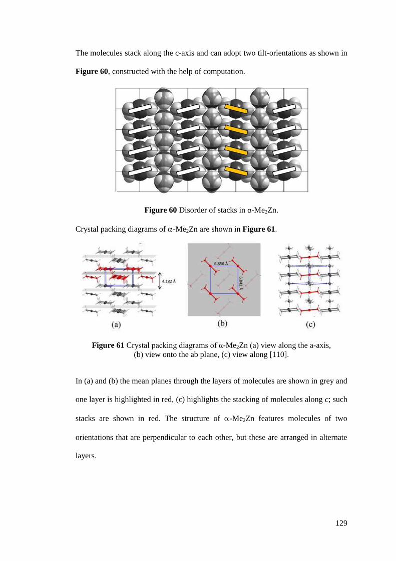
129
The molecules stack along the c-axis and can adopt two tilt-orientations as shown in
Figure 60, constructed with the help of computation.
Figure 60 Disorder of stacks in α-Me2Zn.
Crystal packing diagrams of -Me2Zn are shown in Figure 61.
Figure 61 Crystal packing diagrams of α-Me2Zn (a) view along the a-axis,
(b) view onto the ab plane, (c) view along [110].
In (a) and (b) the mean planes through the layers of molecules are shown in grey and
one layer is highlighted in red, (c) highlights the stacking of molecules along c; such
stacks are shown in red. The structure of -Me2Zn features molecules of two
orientations that are perpendicular to each other, but these are arranged in alternate
layers.
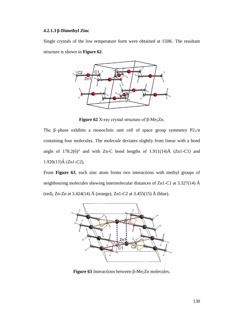
130
4.2.1.3 β-Dimethyl Zinc
Single crystals of the low temperature form were obtained at 150K. The resultant
structure is shown in Figure 62.
Figure 62 X-ray crystal structure of β-Me2Zn.
The β–phase exhibits a monoclinic unit cell of space group symmetry P21/n
containing four molecules. The molecule deviates slightly from linear with a bond
angle of 178.2(6)° and with Zn-C bond lengths of 1.911(14)Å (Zn1-C1) and
1.920(13)Ǻ (Zn1-C2).
From Figure 63, each zinc atom forms two interactions with methyl groups of
neighbouring molecules showing intermolecular distances of Zn1-C1 at 3.327(14) Å
(red), Zn-Zn at 3.424(14) Å (orange), Zn1-C2 at 3.455(15) Å (blue).
Figure 63 Interactions between β-Me2Zn molecules.
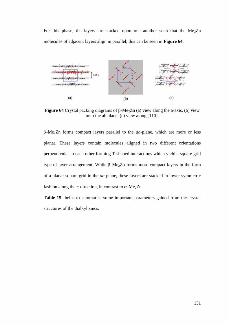
131
For this phase, the layers are stacked upon one another such that the Me2Zn
molecules of adjacent layers align in parallel, this can be seen in Figure 64.
Figure 64 Crystal packing diagrams of β-Me2Zn (a) view along the a-axis, (b) view
onto the ab plane, (c) view along [110].
-Me2Zn forms compact layers parallel to the ab-plane, which are more or less
planar. These layers contain molecules aligned in two different orientations
perpendicular to each other forming T-shaped interactions which yield a square grid
type of layer arrangement. While -Me2Zn forms more compact layers in the form
of a planar square grid in the ab-plane, these layers are stacked in lower symmetric
fashion along the c-direction, in contrast to -Me2Zn.
Table 15 helps to summarise some important parameters gained from the crystal
structures of the dialkyl zincs.
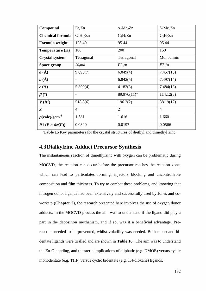
132
Compound Et2Zn -Me2Zn -Me2Zn
Chemical formula C4H10Zn C2H6Zn C2H6Zn
Formula weight 123.49 95.44 95.44
Temperature (K) 100 200 150
Crystal system Tetragonal Tetragonal Monoclinic
Space group I41md P21/n P21/n
a (Å) 9.893(7) 6.849(4) 7.457(13)
b (Å) - 6.842(5) 7.497(14)
c (Å) 5.300(4) 4.182(3) 7.484(13)
(°) - 89.970(11) 114.12(3)
V (Å3) 518.8(6) 196.2(2) 381.9(12)
Z 4 2 4
(calc)/gcm-1
1.581 1.616 1.660
R1 (F > 4(F)) 0.0320 0.0197 0.0566
Table 15 Key parameters for the crystal structures of diethyl and dimethyl zinc.
4.3 Dialkylzinc Adduct Precursor Synthesis
The instantaneous reaction of dimethylzinc with oxygen can be problematic during
MOCVD, the reaction can occur before the precursor reaches the reaction zone,
which can lead to particulates forming, injectors blocking and uncontrollable
composition and film thickness. To try to combat these problems, and knowing that
nitrogen donor ligands had been extensively and successfully used by Jones and co-
workers (Chapter 2), the research presented here involves the use of oxygen donor
adducts. In the MOCVD process the aim was to understand if the ligand did play a
part in the deposition mechanism, and if so, was it a beneficial advantage. Pre-
reaction needed to be prevented, whilst volatility was needed. Both mono and bi-
dentate ligands were trialled and are shown in Table 16 , The aim was to understand
the Zn-O bonding, and the steric implications of aliphatic (e.g. DMOE) versus cyclic
monodentate (e.g. THF) versus cyclic bidentate (e.g. 1,4-dioxane) ligands.
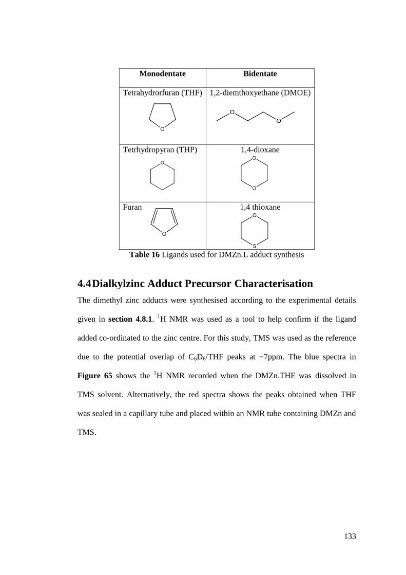
133
Monodentate Bidentate
Tetrahydrorfuran (THF)
1,2-diemthoxyethane (DMOE)
Tetrhydropyran (THP)
1,4-dioxane
Furan
1,4 thioxane
Table 16 Ligands used for DMZn.L adduct synthesis
4.4 Dialkylzinc Adduct Precursor Characterisation
The dimethyl zinc adducts were synthesised according to the experimental details
given in section 4.8.1. 1H NMR was used as a tool to help confirm if the ligand
added co-ordinated to the zinc centre. For this study, TMS was used as the reference
due to the potential overlap of C6D6/THF peaks at ~7ppm. The blue spectra in
Figure 65 shows the 1H NMR recorded when the DMZn.THF was dissolved in
TMS solvent. Alternatively, the red spectra shows the peaks obtained when THF
was sealed in a capillary tube and placed within an NMR tube containing DMZn and
TMS.
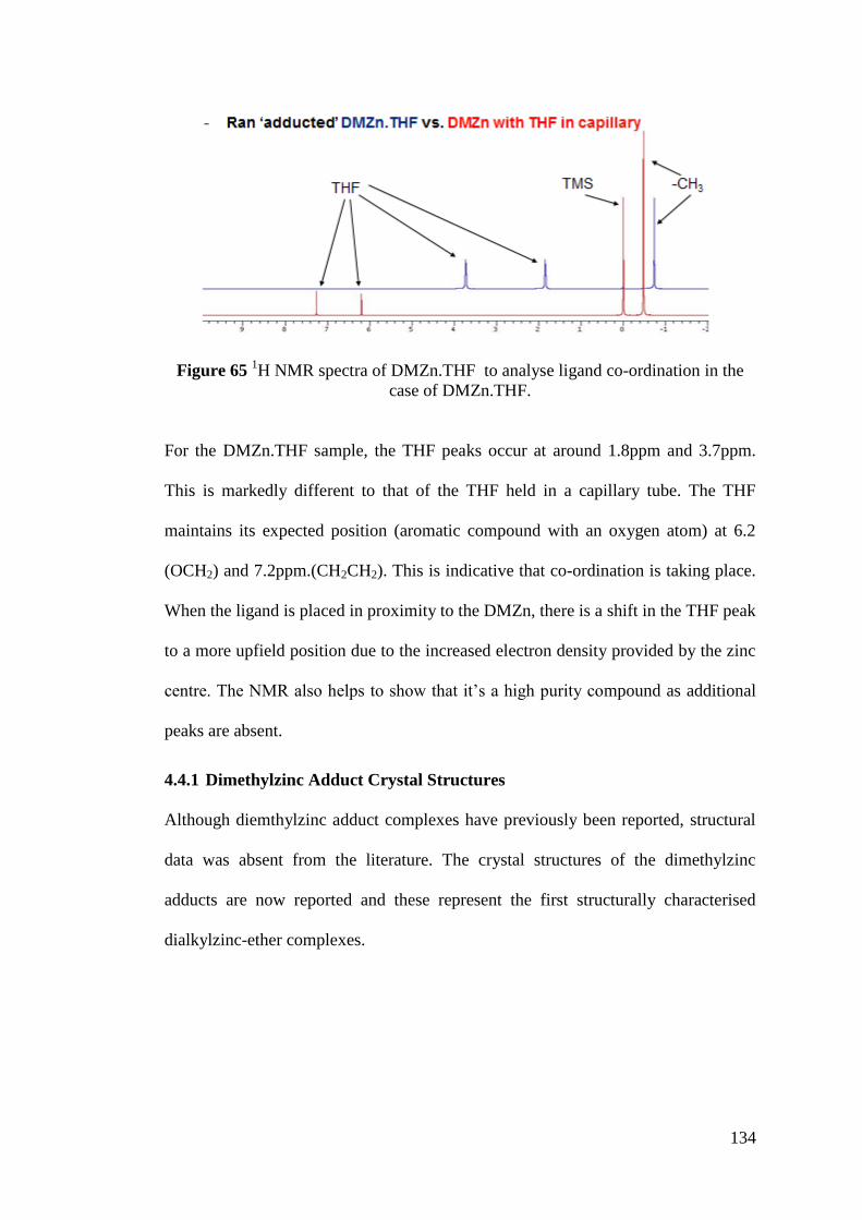
134
Figure 65 1H NMR spectra of DMZn.THF to analyse ligand co-ordination in the
case of DMZn.THF.
For the DMZn.THF sample, the THF peaks occur at around 1.8ppm and 3.7ppm.
This is markedly different to that of the THF held in a capillary tube. The THF
maintains its expected position (aromatic compound with an oxygen atom) at 6.2
(OCH2) and 7.2ppm.(CH2CH2). This is indicative that co-ordination is taking place.
When the ligand is placed in proximity to the DMZn, there is a shift in the THF peak
to a more upfield position due to the increased electron density provided by the zinc
centre. The NMR also helps to show that it’s a high purity compound as additional
peaks are absent.
4.4.1 Dimethylzinc Adduct Crystal Structures
Although diemthylzinc adduct complexes have previously been reported, structural
data was absent from the literature. The crystal structures of the dimethylzinc
adducts are now reported and these represent the first structurally characterised
dialkylzinc-ether complexes.
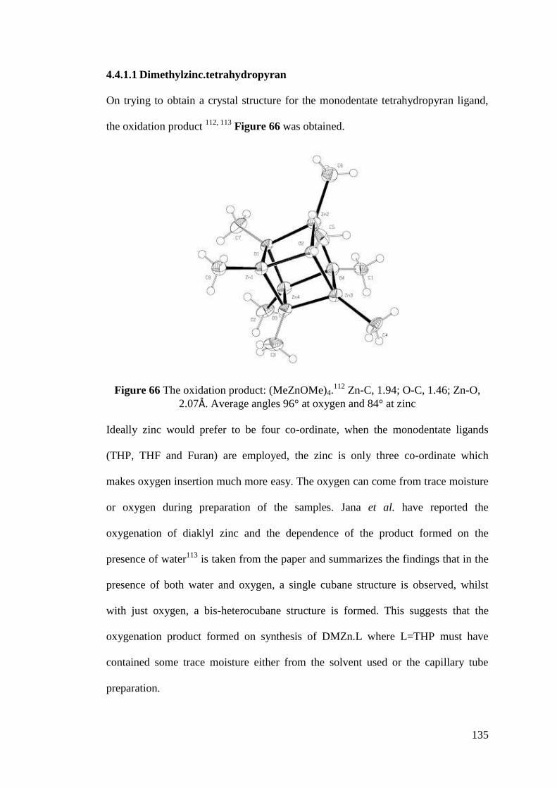
135
4.4.1.1 Dimethylzinc.tetrahydropyran
On trying to obtain a crystal structure for the monodentate tetrahydropyran ligand,
the oxidation product 112, 113
Figure 66 was obtained.
Figure 66 The oxidation product: (MeZnOMe)4.112
Zn-C, 1.94; O-C, 1.46; Zn-O,
2.07Å. Average angles 96° at oxygen and 84° at zinc
Ideally zinc would prefer to be four co-ordinate, when the monodentate ligands
(THP, THF and Furan) are employed, the zinc is only three co-ordinate which
makes oxygen insertion much more easy. The oxygen can come from trace moisture
or oxygen during preparation of the samples. Jana et al. have reported the
oxygenation of diaklyl zinc and the dependence of the product formed on the
presence of water113
is taken from the paper and summarizes the findings that in the
presence of both water and oxygen, a single cubane structure is observed, whilst
with just oxygen, a bis-heterocubane structure is formed. This suggests that the
oxygenation product formed on synthesis of DMZn.L where L=THP must have
contained some trace moisture either from the solvent used or the capillary tube
preparation.
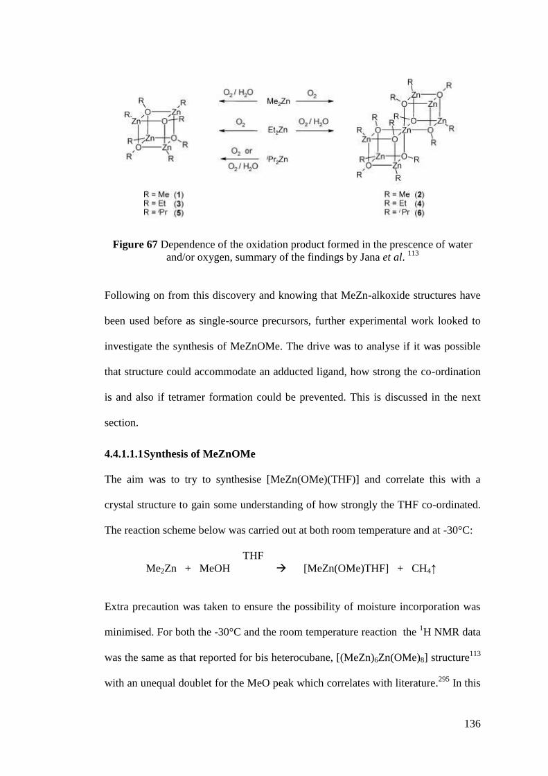
136
Figure 67 Dependence of the oxidation product formed in the prescence of water
and/or oxygen, summary of the findings by Jana et al. 113
Following on from this discovery and knowing that MeZn-alkoxide structures have
been used before as single-source precursors, further experimental work looked to
investigate the synthesis of MeZnOMe. The drive was to analyse if it was possible
that structure could accommodate an adducted ligand, how strong the co-ordination
is and also if tetramer formation could be prevented. This is discussed in the next
section.
4.4.1.1.1 Synthesis of MeZnOMe
The aim was to try to synthesise [MeZn(OMe)(THF)] and correlate this with a
crystal structure to gain some understanding of how strongly the THF co-ordinated.
The reaction scheme below was carried out at both room temperature and at -30°C:
THF
Me2Zn + MeOH [MeZn(OMe)THF] + CH4↑
Extra precaution was taken to ensure the possibility of moisture incorporation was
minimised. For both the -30°C and the room temperature reaction the 1H NMR data
was the same as that reported for bis heterocubane, [(MeZn)6Zn(OMe)8] structure113
with an unequal doublet for the MeO peak which correlates with literature.295
In this
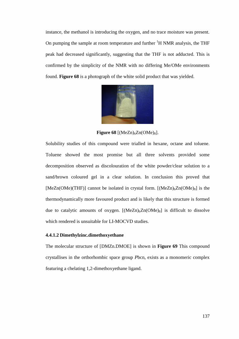
137
instance, the methanol is introducing the oxygen, and no trace moisture was present.
On pumping the sample at room temperature and further 1H NMR analysis, the THF
peak had decreased significantly, suggesting that the THF is not adducted. This is
confirmed by the simplicity of the NMR with no differing Me/OMe environments
found. Figure 68 is a photograph of the white solid product that was yielded.
Figure 68 [(MeZn)6Zn(OMe)8].
Solubility studies of this compound were trialled in hexane, octane and toluene.
Toluene showed the most promise but all three solvents provided some
decomposition observed as discolouration of the white powder/clear solution to a
sand/brown coloured gel in a clear solution. In conclusion this proved that
[MeZn(OMe)(THF)] cannot be isolated in crystal form. [(MeZn)6Zn(OMe)8] is the
thermodynamically more favoured product and is likely that this structure is formed
due to catalytic amounts of oxygen. [(MeZn)6Zn(OMe)8] is difficult to dissolve
which rendered is unsuitable for LI-MOCVD studies.
4.4.1.2 Dimethylzinc.dimethoxyethane
The molecular structure of [DMZn.DMOE] is shown in Figure 69 This compound
crystallises in the orthorhombic space group Pbcn, exists as a monomeric complex
featuring a chelating 1,2-dimethoxyethane ligand.
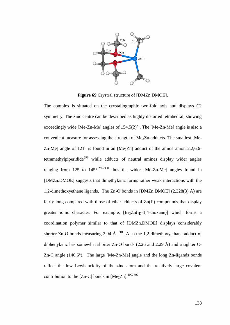
138
Figure 69 Crystral structure of [DMZn.DMOE].
The complex is situated on the crystallographic two-fold axis and displays C2
symmetry. The zinc centre can be described as highly distorted tetrahedral, showing
exceedingly wide [Me-Zn-Me] angles of 154.5(2)° . The [Me-Zn-Me] angle is also a
convenient measure for assessing the strength of Me2Zn-adducts. The smallest [Me-
Zn-Me] angle of 121° is found in an [Me2Zn] adduct of the amide anion 2,2,6,6-
tetramethylpiperidide296
while adducts of neutral amines display wider angles
ranging from 125 to 145°,297-300
thus the wider [Me-Zn-Me] angles found in
[DMZn.DMOE] suggests that dimethylzinc forms rather weak interactions with the
1,2-dimethoxyethane ligands. The Zn-O bonds in [DMZn.DMOE] (2.328(3) Å) are
fairly long compared with those of ether adducts of Zn(II) compounds that display
greater ionic character. For example, [Br2Zn(η2-1,4-dioxane)] which forms a
coordination polymer similar to that of [DMZn.DMOE] displays considerably
shorter Zn-O bonds measuring 2.04 Å. 301
. Also the 1,2-dimethoxyethane adduct of
diphenylzinc has somewhat shorter Zn-O bonds (2.26 and 2.29 Å) and a tighter C-
Zn-C angle (146.6°). The large [Me-Zn-Me] angle and the long Zn-ligands bonds
reflect the low Lewis-acidity of the zinc atom and the relatively large covalent
contribution to the [Zn-C] bonds in [Me2Zn].100, 302
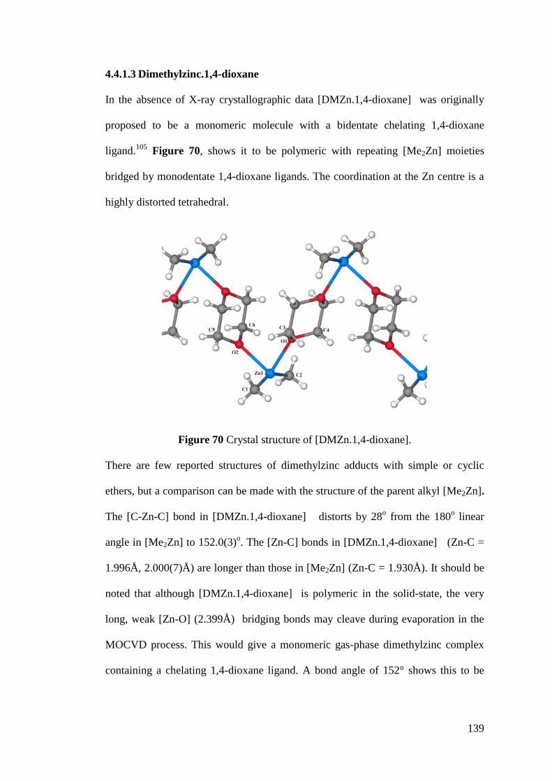
139
4.4.1.3 Dimethylzinc.1,4-dioxane
In the absence of X-ray crystallographic data [DMZn.1,4-dioxane] was originally
proposed to be a monomeric molecule with a bidentate chelating 1,4-dioxane
ligand.105
Figure 70, shows it to be polymeric with repeating [Me2Zn] moieties
bridged by monodentate 1,4-dioxane ligands. The coordination at the Zn centre is a
highly distorted tetrahedral.
Figure 70 Crystal structure of [DMZn.1,4-dioxane].
There are few reported structures of dimethylzinc adducts with simple or cyclic
ethers, but a comparison can be made with the structure of the parent alkyl [Me2Zn].
The [C-Zn-C] bond in [DMZn.1,4-dioxane] distorts by 28o from the 180
o linear
angle in [Me2Zn] to 152.0(3)o. The [Zn-C] bonds in [DMZn.1,4-dioxane] (Zn-C =
1.996Å, 2.000(7)Å) are longer than those in [Me2Zn] (Zn-C = 1.930Å). It should be
noted that although [DMZn.1,4-dioxane] is polymeric in the solid-state, the very
long, weak [Zn-O] (2.399Å) bridging bonds may cleave during evaporation in the
MOCVD process. This would give a monomeric gas-phase dimethylzinc complex
containing a chelating 1,4-dioxane ligand. A bond angle of 152° shows this to be
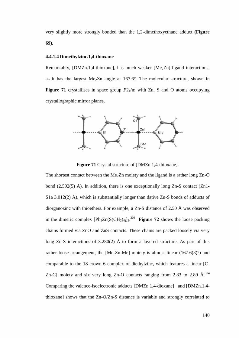
140
very slightly more strongly bonded than the 1,2-dimethoxyethane adduct (Figure
69).
4.4.1.4 Dimethylzinc.1,4-thioxane
Remarkably, [DMZn.1,4-thioxane], has much weaker [Me2Zn]-ligand interactions,
as it has the largest Me2Zn angle at 167.6°. The molecular structure, shown in
Figure 71 crystallises in space group P21/m with Zn, S and O atoms occupying
crystallographic mirror planes.
Figure 71 Crystal structure of [DMZn.1,4-thioxane].
The shortest contact between the Me2Zn moiety and the ligand is a rather long Zn-O
bond (2.592(5) Å). In addition, there is one exceptionally long Zn-S contact (Zn1-
S1a 3.012(2) Å), which is substantially longer than dative Zn-S bonds of adducts of
diorganozinc with thioethers. For example, a Zn-S distance of 2.50 Å was observed
in the dimeric complex [Ph2Zn(S(CH2)4)]2.303
Figure 72 shows the loose packing
chains formed via ZnO and ZnS contacts. These chains are packed loosely via very
long Zn-S interactions of 3.280(2) Å to form a layered structure. As part of this
rather loose arrangement, the [Me-Zn-Me] moiety is almost linear (167.6(3)°) and
comparable to the 18-crown-6 complex of diethylzinc, which features a linear [C-
Zn-C] moiety and six very long Zn-O contacts ranging from 2.83 to 2.89 Å.304
Comparing the valence-isoelectronic adducts [DMZn.1,4-dioxane] and [DMZn.1,4-
thioxane] shows that the Zn-O/Zn-S distance is variable and strongly correlated to
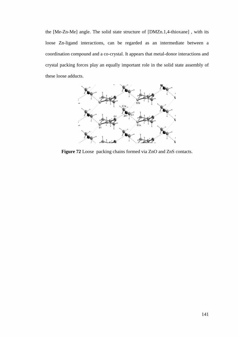
141
the [Me-Zn-Me] angle. The solid state structure of [DMZn.1,4-thioxane] , with its
loose Zn-ligand interactions, can be regarded as an intermediate between a
coordination compound and a co-crystal. It appears that metal-donor interactions and
crystal packing forces play an equally important role in the solid state assembly of
these loose adducts.
Figure 72 Loose packing chains formed via ZnO and ZnS contacts.
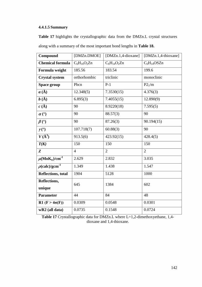
142
4.4.1.5 Summary
Table 17 highlights the crystallographic data from the DMZn.L crystal structures
along with a summary of the most important bond lengths in Table 18.
Compound [DMZn.DMOE] [DMZn.1,4-dioxane] [DMZn.1,4-thioxane]
Chemical formula C6H16O2Zn C6H14O2Zn C6H14OSZn
Formula weight 185.56 183.54 199.6
Crystal system orthorhombic triclinic monoclinic
Space group Pbcn P-1 P21/m
a (Å) 12.348(5) 7.3530(15) 4.376(3)
b (Å) 6.895(3) 7.4055(15) 12.890(9)
c (Å) 90 8.9220(18) 7.595(5)
(°) 90 88.57(3) 90
(°) 90 87.26(3) 90.194(15)
(°) 107.718(7) 60.88(3) 90
V (Å3) 913.5(6) 423.92(15) 428.4(5)
T(K) 150 150 150
Z 4 2 2
(MoK)/cm-1
2.629 2.832 3.035
(calc)/gcm-1
1.349 1.438 1.547
Reflections, total 1904 5128 1000
Reflections,
unique 645 1384 602
Parameter 44 84 48
R1 (F > 4σ(F)) 0.0309 0.0548 0.0301
wR2 (all data) 0.0735 0.1548 0.0724
Table 17 Crystallographic data for DMZn.L where L=1,2-dimethoxyethane, 1,4-
dioxane and 1,4-thioxane.
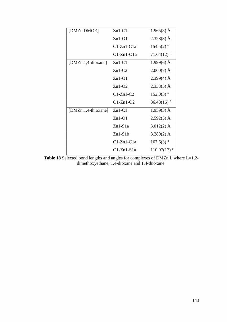
143
[DMZn.DMOE] Zn1-C1 1.965(3) Å
Zn1-O1 2.328(3) Å
C1-Zn1-C1a 154.5(2) °
O1-Zn1-O1a 71.64(12) °
[DMZn.1,4-dioxane] Zn1-C1 1.999(6) Å
Zn1-C2 2.000(7) Å
Zn1-O1 2.399(4) Å
Zn1-O2 2.333(5) Å
C1-Zn1-C2 152.0(3) °
O1-Zn1-O2 86.48(16) °
[DMZn.1,4-thioxane] Zn1-C1 1.959(3) Å
Zn1-O1 2.592(5) Å
Zn1-S1a 3.012(2) Å
Zn1-S1b 3.280(2) Å
C1-Zn1-C1a 167.6(3) °
O1-Zn1-S1a 110.07(17) °
Table 18 Selected bond lengths and angles for complexes of DMZn.L where L=1,2-
dimethoxyethane, 1,4-dioxane and 1,4-thioxane.
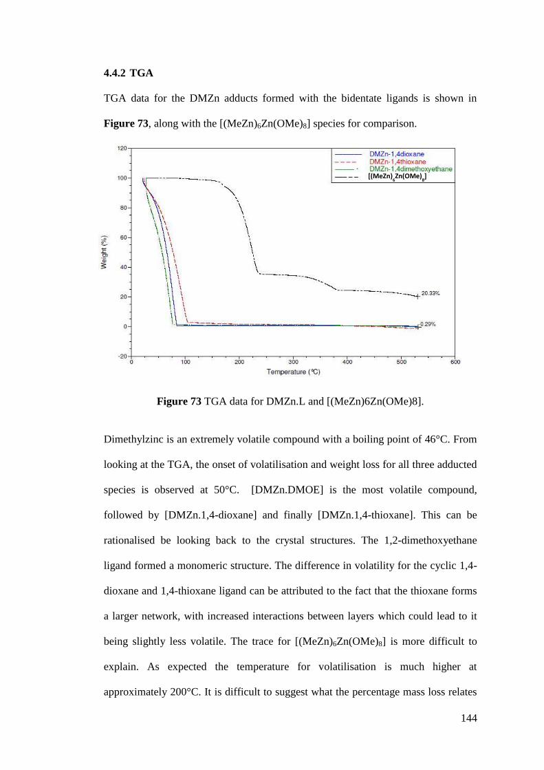
144
4.4.2 TGA
TGA data for the DMZn adducts formed with the bidentate ligands is shown in
Figure 73, along with the [(MeZn)6Zn(OMe)8] species for comparison.
Figure 73 TGA data for DMZn.L and [(MeZn)6Zn(OMe)8].
Dimethylzinc is an extremely volatile compound with a boiling point of 46°C. From
looking at the TGA, the onset of volatilisation and weight loss for all three adducted
species is observed at 50°C. [DMZn.DMOE] is the most volatile compound,
followed by [DMZn.1,4-dioxane] and finally [DMZn.1,4-thioxane]. This can be
rationalised be looking back to the crystal structures. The 1,2-dimethoxyethane
ligand formed a monomeric structure. The difference in volatility for the cyclic 1,4-
dioxane and 1,4-thioxane ligand can be attributed to the fact that the thioxane forms
a larger network, with increased interactions between layers which could lead to it
being slightly less volatile. The trace for [(MeZn)6Zn(OMe)8] is more difficult to
explain. As expected the temperature for volatilisation is much higher at
approximately 200°C. It is difficult to suggest what the percentage mass loss relates
[(MeZn)
6Zn(OMe)
8]
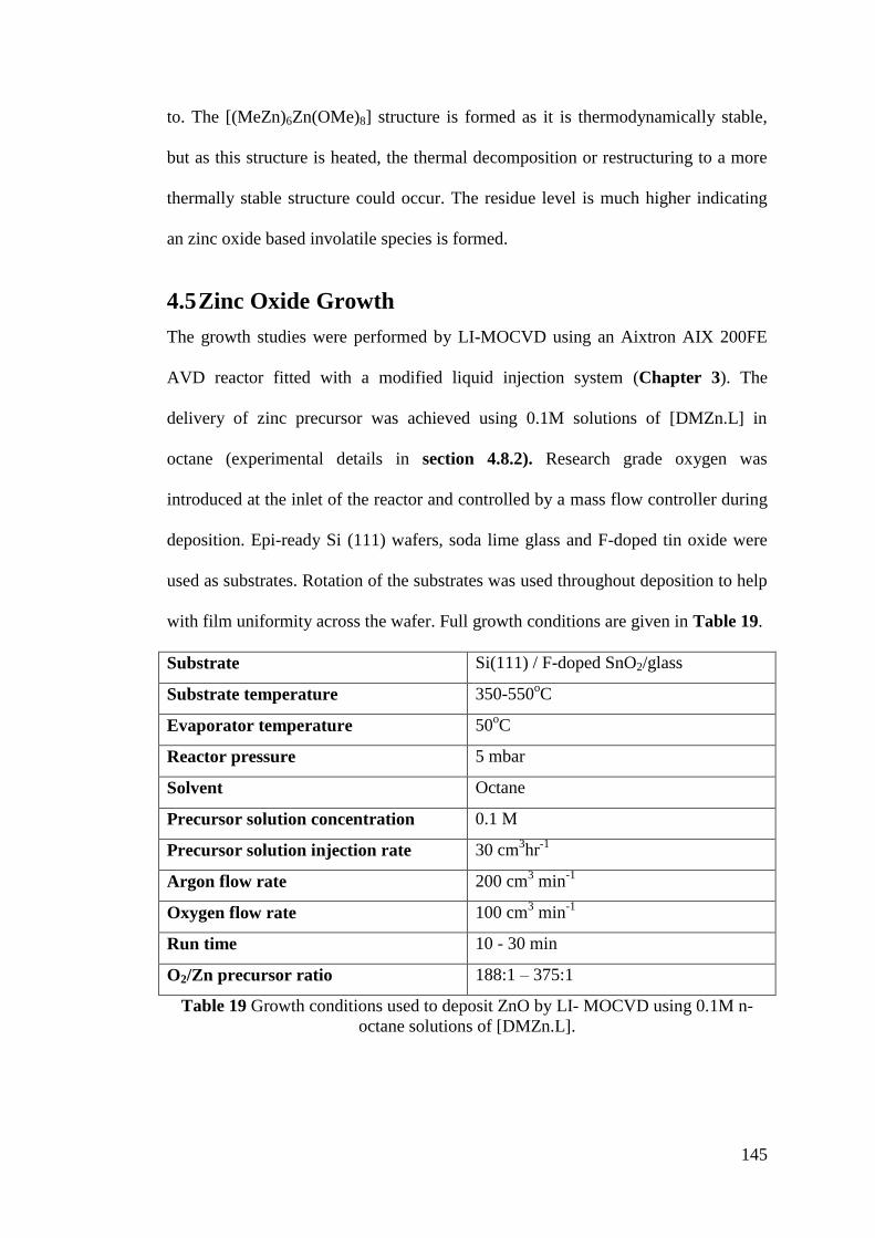
145
to. The [(MeZn)6Zn(OMe)8] structure is formed as it is thermodynamically stable,
but as this structure is heated, the thermal decomposition or restructuring to a more
thermally stable structure could occur. The residue level is much higher indicating
an zinc oxide based involatile species is formed.
4.5 Zinc Oxide Growth
The growth studies were performed by LI-MOCVD using an Aixtron AIX 200FE
AVD reactor fitted with a modified liquid injection system (Chapter 3). The
delivery of zinc precursor was achieved using 0.1M solutions of [DMZn.L] in
octane (experimental details in section 4.8.2). Research grade oxygen was
introduced at the inlet of the reactor and controlled by a mass flow controller during
deposition. Epi-ready Si (111) wafers, soda lime glass and F-doped tin oxide were
used as substrates. Rotation of the substrates was used throughout deposition to help
with film uniformity across the wafer. Full growth conditions are given in Table 19.
Substrate Si(111) / F-doped SnO2/glass
Substrate temperature 350-550oC
Evaporator temperature 50oC
Reactor pressure 5 mbar
Solvent Octane
Precursor solution concentration 0.1 M
Precursor solution injection rate 30 cm3hr
-1
Argon flow rate 200 cm3 min
-1
Oxygen flow rate 100 cm3 min
-1
Run time 10 - 30 min
O2/Zn precursor ratio 188:1 – 375:1
Table 19 Growth conditions used to deposit ZnO by LI- MOCVD using 0.1M n-
octane solutions of [DMZn.L].
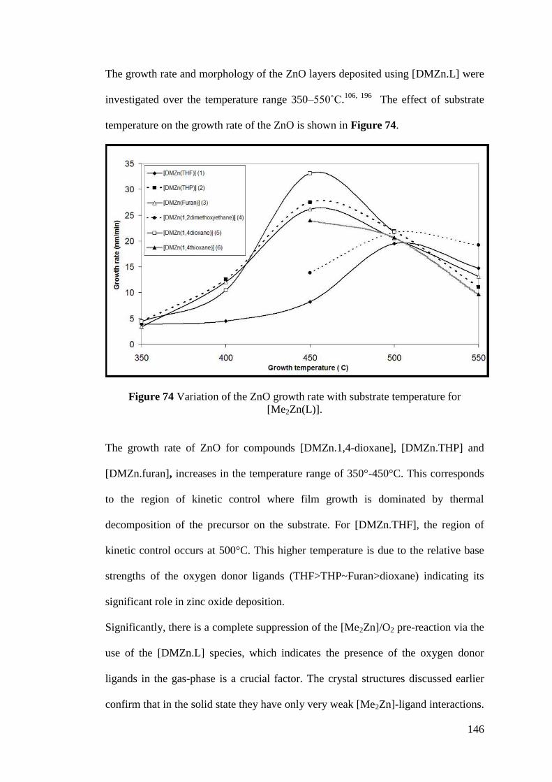
146
The growth rate and morphology of the ZnO layers deposited using [DMZn.L] were
investigated over the temperature range 350–550˚C.106, 196
The effect of substrate
temperature on the growth rate of the ZnO is shown in Figure 74.
Figure 74 Variation of the ZnO growth rate with substrate temperature for
[Me2Zn(L)].
The growth rate of ZnO for compounds [DMZn.1,4-dioxane], [DMZn.THP] and
[DMZn.furan], increases in the temperature range of 350°-450°C. This corresponds
to the region of kinetic control where film growth is dominated by thermal
decomposition of the precursor on the substrate. For [DMZn.THF], the region of
kinetic control occurs at 500°C. This higher temperature is due to the relative base
strengths of the oxygen donor ligands (THF>THP~Furan>dioxane) indicating its
significant role in zinc oxide deposition.
Significantly, there is a complete suppression of the [Me2Zn]/O2 pre-reaction via the
use of the [DMZn.L] species, which indicates the presence of the oxygen donor
ligands in the gas-phase is a crucial factor. The crystal structures discussed earlier
confirm that in the solid state they have only very weak [Me2Zn]-ligand interactions.
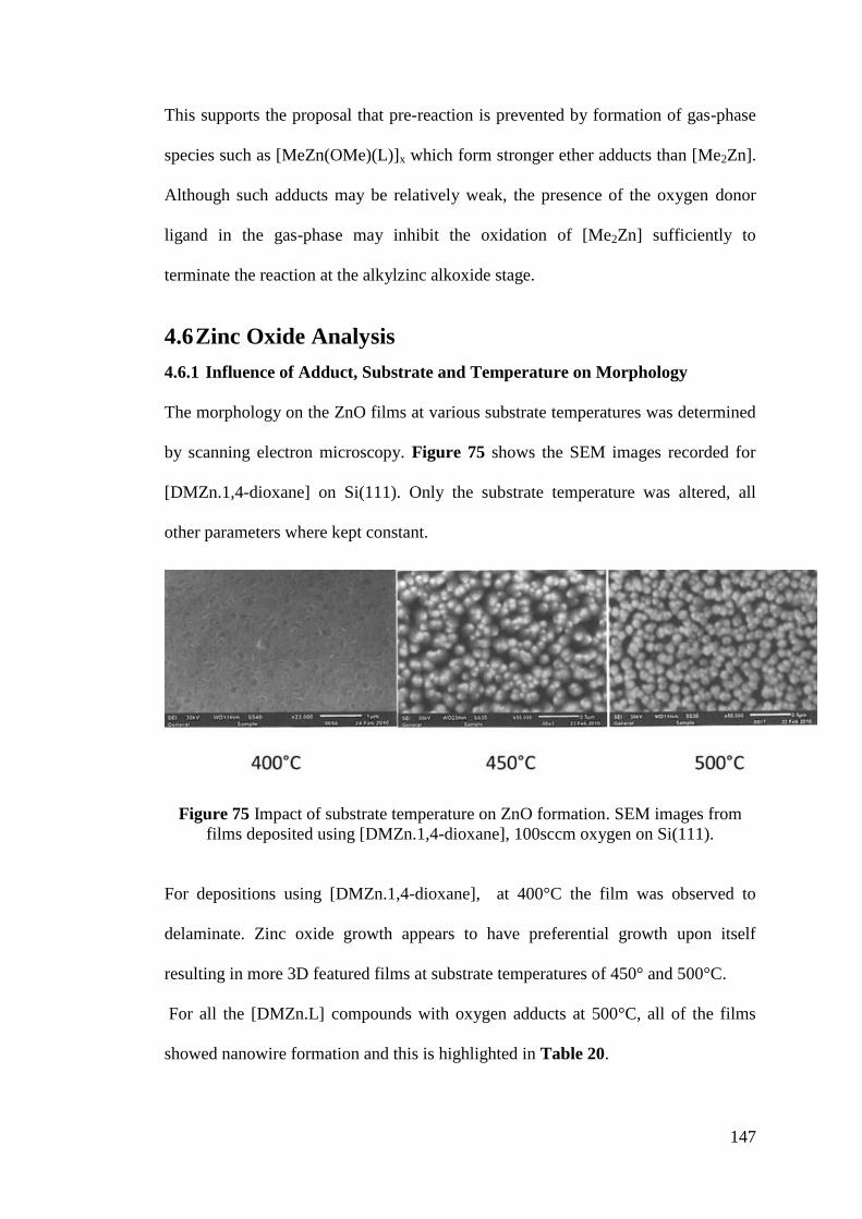
147
This supports the proposal that pre-reaction is prevented by formation of gas-phase
species such as [MeZn(OMe)(L)]x which form stronger ether adducts than [Me2Zn].
Although such adducts may be relatively weak, the presence of the oxygen donor
ligand in the gas-phase may inhibit the oxidation of [Me2Zn] sufficiently to
terminate the reaction at the alkylzinc alkoxide stage.
4.6 Zinc Oxide Analysis
4.6.1 Influence of Adduct, Substrate and Temperature on Morphology
The morphology on the ZnO films at various substrate temperatures was determined
by scanning electron microscopy. Figure 75 shows the SEM images recorded for
[DMZn.1,4-dioxane] on Si(111). Only the substrate temperature was altered, all
other parameters where kept constant.
Figure 75 Impact of substrate temperature on ZnO formation. SEM images from
films deposited using [DMZn.1,4-dioxane], 100sccm oxygen on Si(111).
For depositions using [DMZn.1,4-dioxane], at 400°C the film was observed to
delaminate. Zinc oxide growth appears to have preferential growth upon itself
resulting in more 3D featured films at substrate temperatures of 450° and 500°C.
For all the [DMZn.L] compounds with oxygen adducts at 500°C, all of the films
showed nanowire formation and this is highlighted in Table 20.
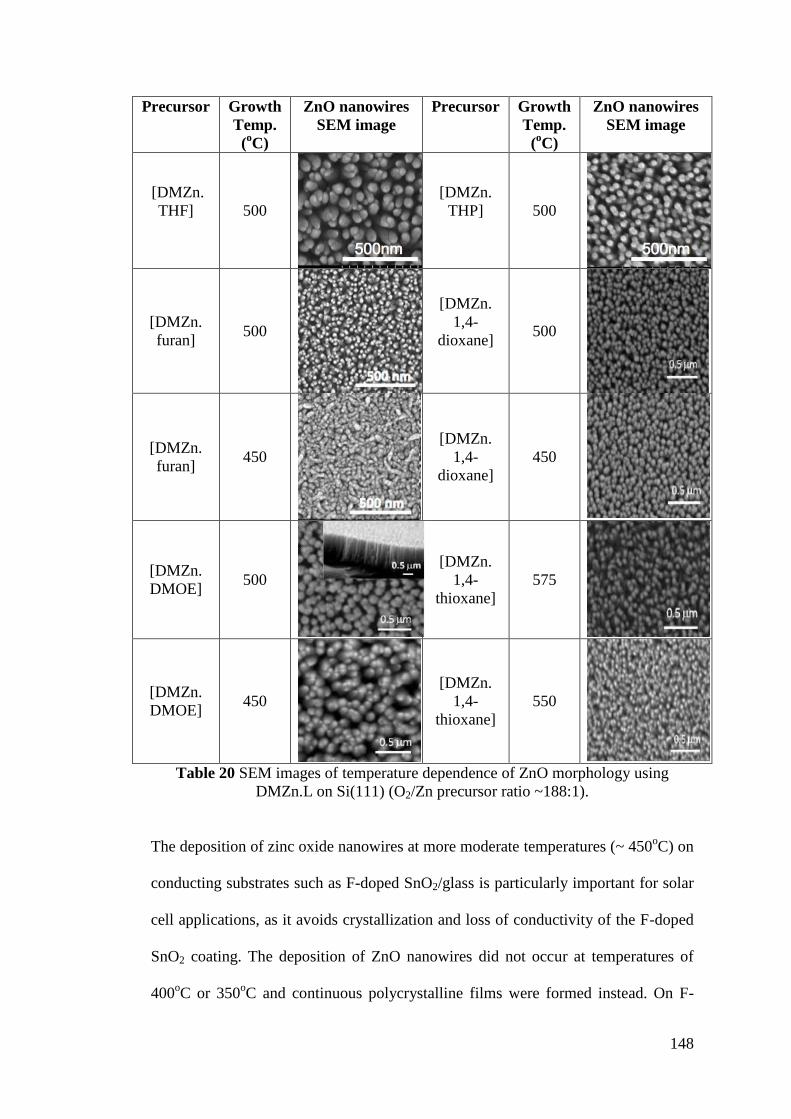
148
Precursor Growth
Temp.
(oC)
ZnO nanowires
SEM image
Precursor Growth
Temp.
(oC)
ZnO nanowires
SEM image
[DMZn.
THF]
500
[DMZn.
THP]
500
[DMZn.
furan] 500
[DMZn.
1,4-
dioxane]
500
[DMZn.
furan] 450
[DMZn.
1,4-
dioxane]
450
[DMZn.
DMOE] 500
[DMZn.
1,4-
thioxane]
575
[DMZn.
DMOE] 450
[DMZn.
1,4-
thioxane]
550
Table 20 SEM images of temperature dependence of ZnO morphology using
DMZn.L on Si(111) (O2/Zn precursor ratio ~188:1).
The deposition of zinc oxide nanowires at more moderate temperatures (~ 450oC) on
conducting substrates such as F-doped SnO2/glass is particularly important for solar
cell applications, as it avoids crystallization and loss of conductivity of the F-doped
SnO2 coating. The deposition of ZnO nanowires did not occur at temperatures of
400oC or 350
oC and continuous polycrystalline films were formed instead. On F-
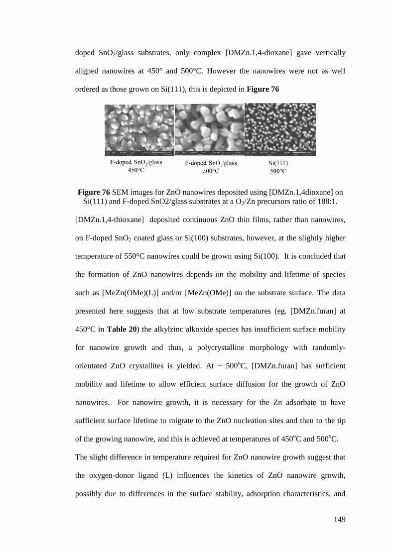
149
doped SnO2/glass substrates, only complex [DMZn.1,4-dioxane] gave vertically
aligned nanowires at 450° and 500°C. However the nanowires were not as well
ordered as those grown on Si(111), this is depicted in Figure 76
Figure 76 SEM images for ZnO nanowires deposited using [DMZn.1,4dioxane] on
Si(111) and F-doped SnO2/glass substrates at a O2/Zn precursors ratio of 188:1.
[DMZn.1,4-thioxane] deposited continuous ZnO thin films, rather than nanowires,
on F-doped SnO2 coated glass or Si(100) substrates, however, at the slightly higher
temperature of 550°C nanowires could be grown using Si(100). It is concluded that
the formation of ZnO nanowires depends on the mobility and lifetime of species
such as [MeZn(OMe)(L)] and/or [MeZn(OMe)] on the substrate surface. The data
presented here suggests that at low substrate temperatures (eg. [DMZn.furan] at
450°C in Table 20) the alkylzinc alkoxide species has insufficient surface mobility
for nanowire growth and thus, a polycrystalline morphology with randomly-
orientated ZnO crystallites is yielded. At ~ 500oC, [DMZn.furan] has sufficient
mobility and lifetime to allow efficient surface diffusion for the growth of ZnO
nanowires. For nanowire growth, it is necessary for the Zn adsorbate to have
sufficient surface lifetime to migrate to the ZnO nucleation sites and then to the tip
of the growing nanowire, and this is achieved at temperatures of 450oC and 500
oC.
The slight difference in temperature required for ZnO nanowire growth suggest that
the oxygen-donor ligand (L) influences the kinetics of ZnO nanowire growth,
possibly due to differences in the surface stability, adsorption characteristics, and
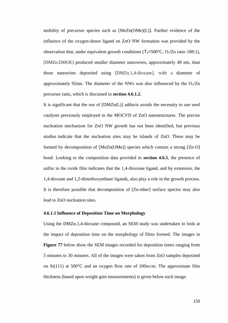
150
mobility of precursor species such as [MeZn(OMe)(L)]. Further evidence of the
influence of the oxygen-donor ligand on ZnO NW formation was provided by the
observation that, under equivalent growth conditions (Tg=500°C, O2/Zn ratio 188:1),
[DMZn.DMOE] produced smaller diameter nanowires, approximately 49 nm, than
those nanowires deposited using [DMZn.1,4-dioxane], with a diameter of
approximately 92nm. The diameter of the NWs was also influenced by the O2/Zn
precursor ratio, which is discussed in section 4.6.1.2.
It is significant that the use of [DMZn(L)] adducts avoids the necessity to use seed
catalysts previously employed in the MOCVD of ZnO nanostructures. The precise
nucleation mechanism for ZnO NW growth has not been identified, but previous
studies indicate that the nucleation sites may be islands of ZnO. These may be
formed by decomposition of [MeZn(OMe)] species which contain a strong [Zn-O]
bond. Looking to the composition data provided in section 4.6.5, the presence of
sulfur in the oxide film indicates that the 1,4-thioxane ligand, and by extension, the
1,4-dioxane and 1,2-dimethoxyethane ligands, also play a role in the growth process.
It is therefore possible that decomposition of [Zn-ether] surface species may also
lead to ZnO nucleation sites.
4.6.1.1 Influence of Deposition Time on Morphology
Using the DMZn.1,4-dioxane compound, an SEM study was undertaken to look at
the impact of deposition time on the morphology of films formed. The images in
Figure 77 below show the SEM images recorded for deposition times ranging from
5 minutes to 30 minutes. All of the images were taken from ZnO samples deposited
on Si(111) at 500°C and an oxygen flow rate of 100sccm. The approximate film
thickness (based upon weight gain measurements) is given below each image.
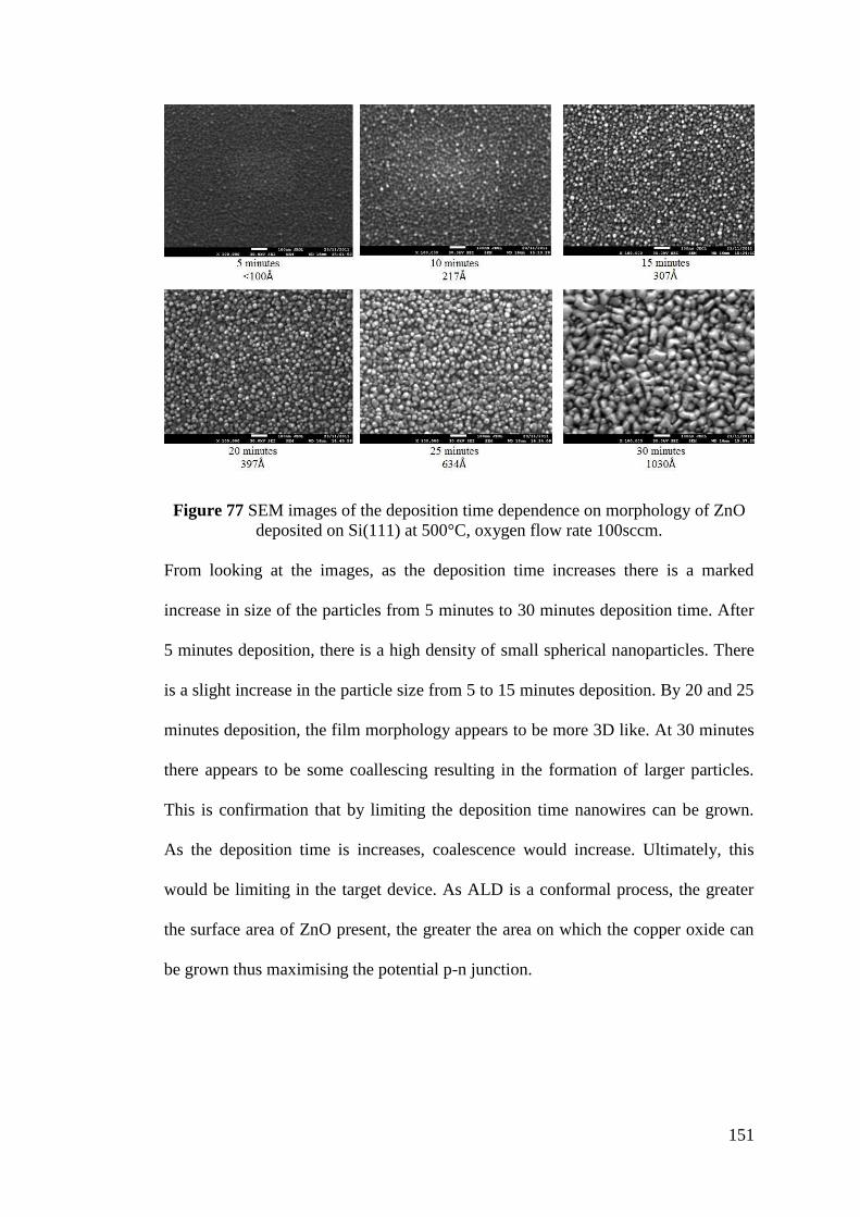
151
Figure 77 SEM images of the deposition time dependence on morphology of ZnO
deposited on Si(111) at 500°C, oxygen flow rate 100sccm.
From looking at the images, as the deposition time increases there is a marked
increase in size of the particles from 5 minutes to 30 minutes deposition time. After
5 minutes deposition, there is a high density of small spherical nanoparticles. There
is a slight increase in the particle size from 5 to 15 minutes deposition. By 20 and 25
minutes deposition, the film morphology appears to be more 3D like. At 30 minutes
there appears to be some coallescing resulting in the formation of larger particles.
This is confirmation that by limiting the deposition time nanowires can be grown.
As the deposition time is increases, coalescence would increase. Ultimately, this
would be limiting in the target device. As ALD is a conformal process, the greater
the surface area of ZnO present, the greater the area on which the copper oxide can
be grown thus maximising the potential p-n junction.
152
4.6.1.2 Influence of Oxygen:Zinc Ratio
So far it has been shown that the formation of nanowires is dependant upon substrate
temperature, deposition time and substrate. A further parameter investigated was the
impact of the oxygen:zinc ratio. Table 21 shows the oxygen flow rate used during
deposition for the [DMZn.1,4-dioxane] compound, with the SEM images for these
samples shown in Figure 78.
Substrate Growth
Temperature
(°C)
O2
flow
rate
(sccm)
O2:Zn
ratio
ZnO morphology
(SEM)
Average
nanowire
diameter
(nm)
Si(111) 500
500
500
175
150
100
340:1
276:1
187:1
Nanowires
Nanowires
Nanowires
120
120
92
Table 21 Summary of oxygen flow rates and subsequent O2:Zn ratio.
Figure 78 SEM images analysing the impact of oxygen flow rate on the morphology
of ZnO on Si(111) at 500°C using [DMZn.1,4-dioxane].
The SEM images appear to show that as the oxygen decreases the packing density
increases. With large VI/II precursor ratios, generally larger diameter ZnO
nanowires were formed, as highlighted in Table 21.
4.6.1.3 Summary of Morphology
Table 22 summarizes the film morphology of ZnO deposited from DMZn.L and O2
as discussed in this section
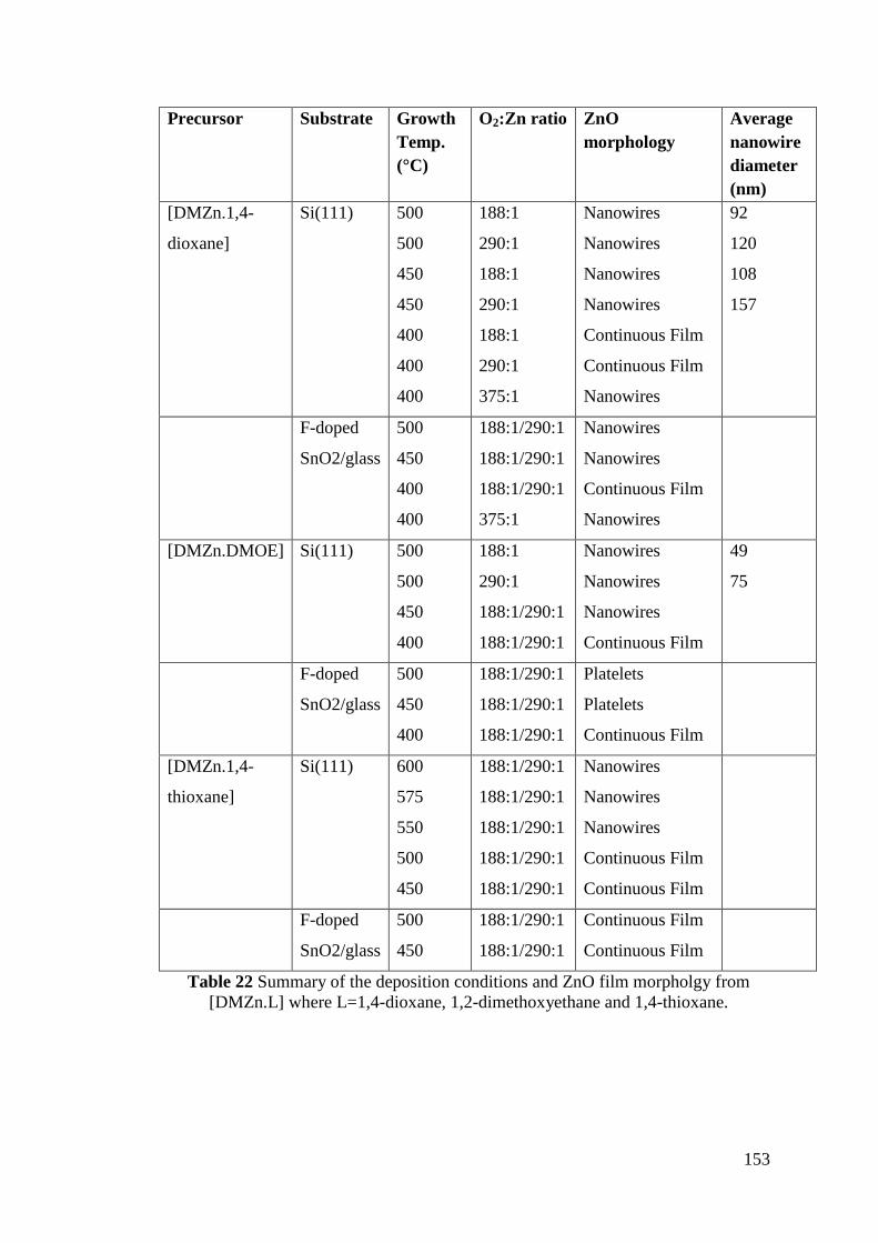
153
Precursor Substrate Growth
Temp.
(°C)
O2:Zn ratio ZnO
morphology
Average
nanowire
diameter
(nm)
[DMZn.1,4-
dioxane]
Si(111) 500
500
450
450
400
400
400
188:1
290:1
188:1
290:1
188:1
290:1
375:1
Nanowires
Nanowires
Nanowires
Nanowires
Continuous Film
Continuous Film
Nanowires
92
120
108
157
F-doped
SnO2/glass
500
450
400
400
188:1/290:1
188:1/290:1
188:1/290:1
375:1
Nanowires
Nanowires
Continuous Film
Nanowires
[DMZn.DMOE] Si(111) 500
500
450
400
188:1
290:1
188:1/290:1
188:1/290:1
Nanowires
Nanowires
Nanowires
Continuous Film
49
75
F-doped
SnO2/glass
500
450
400
188:1/290:1
188:1/290:1
188:1/290:1
Platelets
Platelets
Continuous Film
[DMZn.1,4-
thioxane]
Si(111) 600
575
550
500
450
188:1/290:1
188:1/290:1
188:1/290:1
188:1/290:1
188:1/290:1
Nanowires
Nanowires
Nanowires
Continuous Film
Continuous Film
F-doped
SnO2/glass
500
450
188:1/290:1
188:1/290:1
Continuous Film
Continuous Film
Table 22 Summary of the deposition conditions and ZnO film morpholgy from
[DMZn.L] where L=1,4-dioxane, 1,2-dimethoxyethane and 1,4-thioxane.
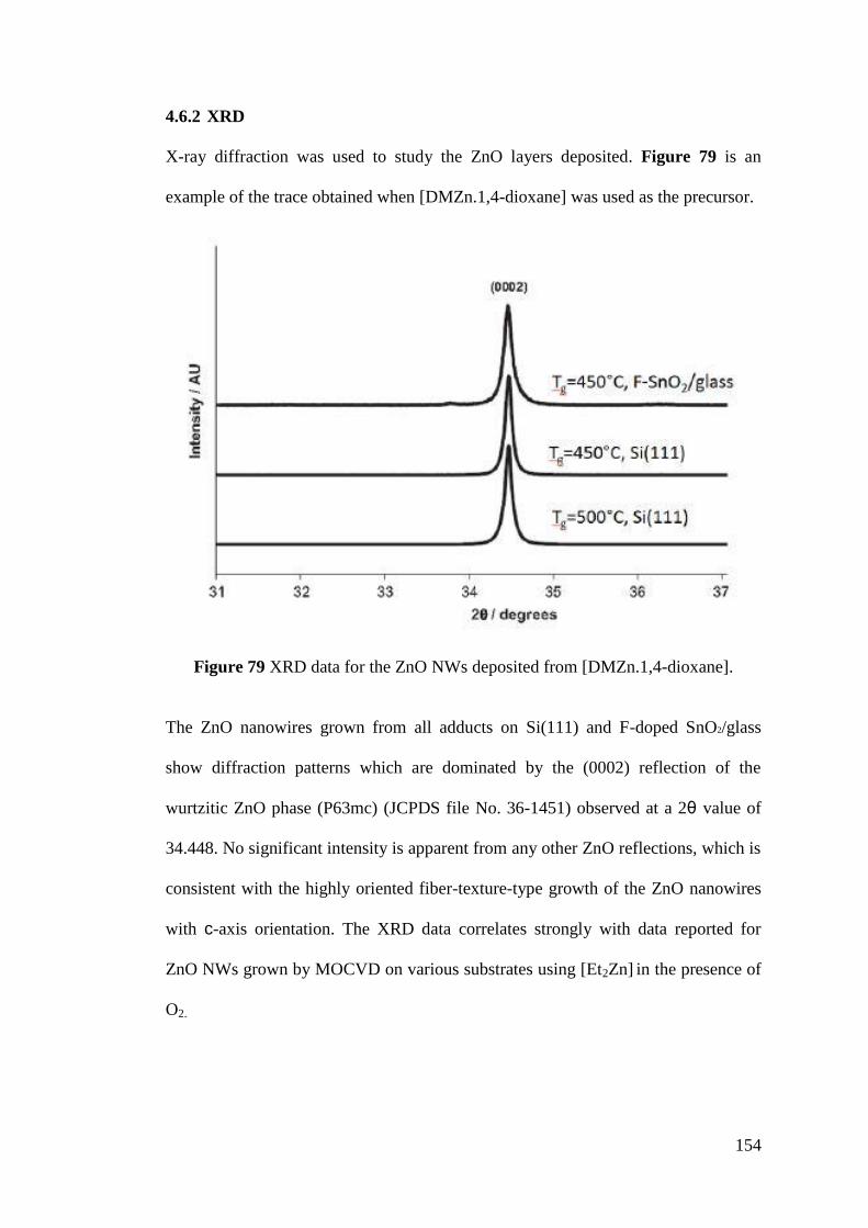
154
4.6.2 XRD
X-ray diffraction was used to study the ZnO layers deposited. Figure 79 is an
example of the trace obtained when [DMZn.1,4-dioxane] was used as the precursor.
Figure 79 XRD data for the ZnO NWs deposited from [DMZn.1,4-dioxane].
The ZnO nanowires grown from all adducts on Si(111) and F-doped SnO2/glass
show diffraction patterns which are dominated by the (0002) reflection of the
wurtzitic ZnO phase (P63mc) (JCPDS file No. 36-1451) observed at a 2θ value of
34.448. No significant intensity is apparent from any other ZnO reflections, which is
consistent with the highly oriented fiber-texture-type growth of the ZnO nanowires
with c-axis orientation. The XRD data correlates strongly with data reported for
ZnO NWs grown by MOCVD on various substrates using [Et2Zn] in the presence of
O2.
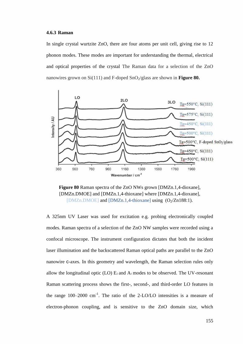
155
4.6.3 Raman
In single crystal wurtzite ZnO, there are four atoms per unit cell, giving rise to 12
phonon modes. These modes are important for understanding the thermal, electrical
and optical properties of the crystal The Raman data for a selection of the ZnO
nanowires grown on Si(111) and F-doped SnO2/glass are shown in Figure 80.
Figure 80 Raman spectra of the ZnO NWs grown [DMZn.1,4-dioxane],
[DMZn.DMOE] and [DMZn.1,4-thioxane] where [DMZn.1,4-dioxane],
[DMZn.DMOE] and [DMZn.1,4-thioxane] using (O2/Zn188:1).
A 325nm UV Laser was used for excitation e.g. probing electronically coupled
modes. Raman spectra of a selection of the ZnO NW samples were recorded using a
confocal microscope. The instrument configuration dictates that both the incident
laser illumination and the backscattered Raman optical paths are parallel to the ZnO
nanowire c-axes. In this geometry and wavelength, the Raman selection rules only
allow the longitudinal optic (LO) E2 and A1 modes to be observed. The UV-resonant
Raman scattering process shows the first-, second-, and third-order LO features in
the range 100–2000 cm-1
. The ratio of the 2-LO/LO intensities is a measure of
electron-phonon coupling, and is sensitive to the ZnO domain size, which
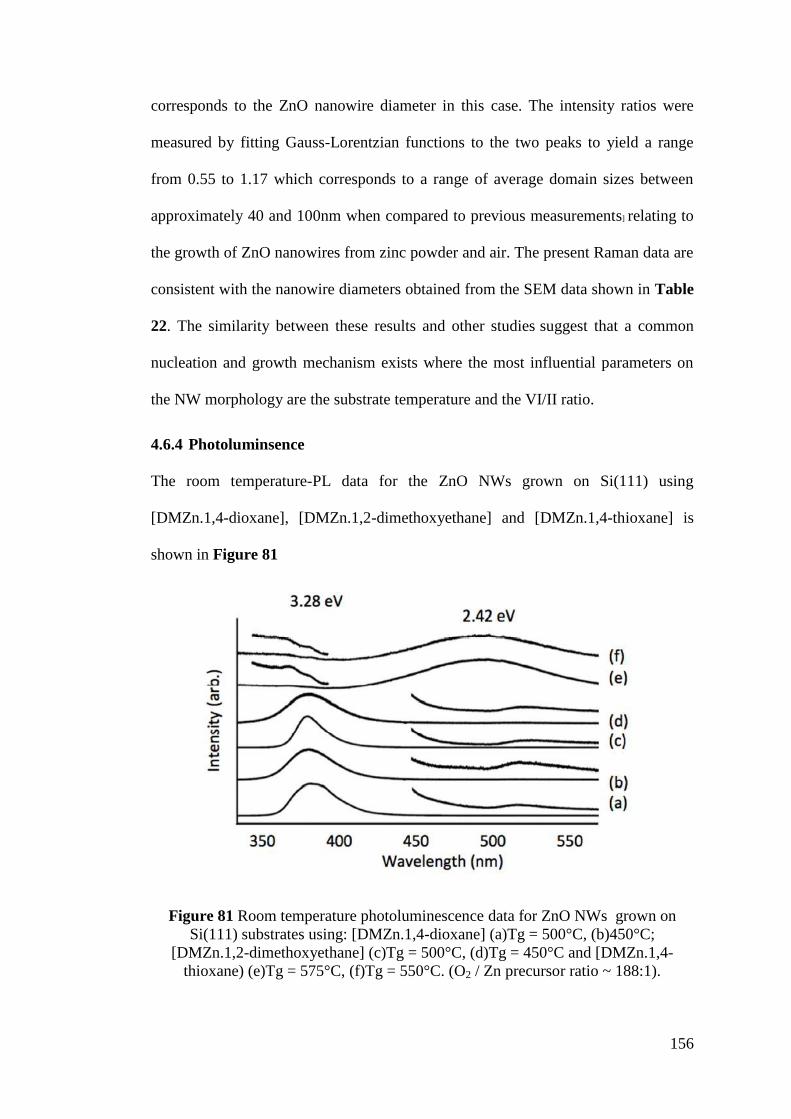
156
corresponds to the ZnO nanowire diameter in this case. The intensity ratios were
measured by fitting Gauss-Lorentzian functions to the two peaks to yield a range
from 0.55 to 1.17 which corresponds to a range of average domain sizes between
approximately 40 and 100nm when compared to previous measurements] relating to
the growth of ZnO nanowires from zinc powder and air. The present Raman data are
consistent with the nanowire diameters obtained from the SEM data shown in Table
22. The similarity between these results and other studies suggest that a common
nucleation and growth mechanism exists where the most influential parameters on
the NW morphology are the substrate temperature and the VI/II ratio.
4.6.4 Photoluminsence
The room temperature-PL data for the ZnO NWs grown on Si(111) using
[DMZn.1,4-dioxane], [DMZn.1,2-dimethoxyethane] and [DMZn.1,4-thioxane] is
shown in Figure 81
Figure 81 Room temperature photoluminescence data for ZnO NWs grown on
Si(111) substrates using: [DMZn.1,4-dioxane] (a)Tg = 500°C, (b)450°C;
[DMZn.1,2-dimethoxyethane] (c)Tg = 500°C, (d)Tg = 450°C and [DMZn.1,4-
thioxane) (e)Tg = 575°C, (f)Tg = 550°C. (O2 / Zn precursor ratio ~ 188:1).
157
The data for the ZnO NWs derived from [DMZn.1,4-dioxane] and [DMZn.1,2-
dimethoxyethane], Figure 81 a-d, show an intense peak at 3.28 eV, attributable to
near band-edge emission arising from the recombination of free excitons, with very
low intensity green luminescence at 2.42 eV. This data also shows that the ZnO
NWs grown from these compounds have a high degree of crystalline quality and are
high purity with a low defect density. The PL data presented here is identical to the
room temperature PL data for ZnO NWs grown at 500 °C on Si(111) substrates
using [DMZn.L] (L=THF, THP, furan). The PL data shown in Figure 81 a-d are
also very similar to PL data for high quality ZnO NWs grown by MOCVD using
[Et2Zn] and O2 which is dominated by near band-edge emission with negligible
defect-related green emission. The 2.42 eV defect-related emission peaks in the
room temperature PL spectra for ZnO NWs grown using the [DMZn(bidentate
ether)] adducts are significantly less intense than reported in PL data in some studies
of ZnO NWs grown by other techniques, such as hydrothermal deposition. This
demonstrates the excellent photonic properties of the ZnO NWs grown from the
dimethylzinc adducts. In marked contrast, for [DMZn.1,4-thioxane] the room
temperature PL data for the ZnO NWs grown at 550 °C and 575°C on Si(111),
(Figure 81e and f), is dominated by defect-related emission at 2.42 eV, with the
near band-edge emission peak at 3.28 eV being barely detectable above the
background level. This suggests that the ZnO NWs grown from [DMZn.1,4-
thioxane] contain a very high level of oxygen defects. In addition, the near band-
edge emission peak has ‘blue-shifted’ to higher energy, which can be attributed to
the Burstein–Moss effect and is explained by the filling of ZnO density of states,
near the conduction-band minimum, with sulphur-induced excessive charge carriers.
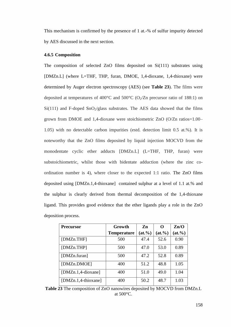
158
This mechanism is confirmed by the presence of 1 at.-% of sulfur impurity detected
by AES discussed in the next section.
4.6.5 Composition
The composition of selected ZnO films deposited on Si(111) substrates using
[DMZn.L] (where L=THF, THP, furan, DMOE, 1,4-dioxane, 1,4-thioxane) were
determined by Auger electron spectroscopy (AES) (see Table 23). The films were
deposited at temperatures of 400°C and 500°C (O2/Zn precursor ratio of 188:1) on
Si(111) and F-doped SnO2/glass substrates. The AES data showed that the films
grown from DMOE and 1,4-dioxane were stoichiometric ZnO (O/Zn ratios=1.00–
1.05) with no detectable carbon impurities (estd. detection limit 0.5 at.%). It is
noteworthy that the ZnO films deposited by liquid injection MOCVD from the
monodentate cyclic ether adducts [DMZn.L] (L=THF, THP, furan) were
substoichiometric, whilst those with bidentate adduction (where the zinc co-
ordination number is 4), where closer to the expected 1:1 ratio. The ZnO films
deposited using [DMZn.1,4-thioxane] contained sulphur at a level of 1.1 at.% and
the sulphur is clearly derived from thermal decomposition of the 1,4-thioxane
ligand. This provides good evidence that the ether ligands play a role in the ZnO
deposition process.
Precursor Growth
Temperature
Zn
(at.%)
O
(at.%)
Zn/O
(at.%)
[DMZn.THF] 500 47.4 52.6 0.90
[DMZn.THP] 500 47.0 53.0 0.89
[DMZn.furan] 500 47.2 52.8 0.89
[DMZn.DMOE] 400 51.2 48.8 1.05
[DMZn.1,4-dioxane] 400 51.0 49.0 1.04
[DMZn.1,4-thioxane] 400 50.2 48.7 1.03
Table 23 The composition of ZnO nanowires deposited by MOCVD from DMZn.L
at 500°C.
159
The data presented herein is further evidence for the crucial role played by oxygen-
donor ligands in preventing the [Me2Zn]/O2 pre-reaction, and in facilitating ZnO
NW growth. The crystal structures indicate that there are only very weak
interactions between [Me2Zn] and the donor ligands. This strongly supports the
proposal that prevention of pre-reaction is not due to simple blocking of the reactive
Zn centre by associated gas-phase adducts of the type [Me2Zn. ether]. The weak
[Me2Zn]-ether interactions suggest that the complexes may be only loosely
associated in the gas phase during the MOCVD process. It is thus more probable
that pre-reactions are prevented by formation of gas-phase intermediate species such
as [MeZn(OMe)(L)]x which form stronger adducts with the donor ligand (L) than
[Me2Zn]. The crystal structure of the relatively oxygen-inert complex
[tBuZn(O
tBu)(THF)]2 may serve as a model for the intermediate species
[MeZn(OMe)(L)]. Its [Zn-THF] bonds are shorter (2.239Å) than the [Zn-ether]
bonds in the adducts THF,THP and furan, indicative of a higher [Zn-ether] bond
strength.
4.7 Conclusions
In summary, this chapter has highlighted the single crystal x-ray diffraction results
for DEZn and DMZn. Single crystal XRD data for [DMZn.L] helps to shows that
[Me2Zn] forms weak adducts with ether ligands. The 1,4-dioxane complex is
polymeric with repeating [Me2Zn] units bridged by 1,4-dioxane ligands. By contrast
the 1,2-dimethoxyethane complex has a monomeric structure containing a bidentate
and chelating ligands. The 1,4-thioxane precursor forms even weaker interactions
with [Me2Zn] and the solid-state structure can be regarded as an intermediate
between a coordination complex and a co-crystal. It has been demonstrated that the
oxygen containing adducts [DMZn.L] (L = THF, THP, Furan, 1,2-dimethoxyethane,
160
1,4-dioxane and 1,4-thioxane) avoid the pre-reaction between [Me2Zn] and oxygen.
The suppression of gas-phase pre-reaction by the [DMZn.L] and the probable
existence of alkylzinc alkoxide surface species, such as [MeZn(OMe)], allows the
controlled growth of high-purity ZnO nanowires in a narrow growth temperature
range centred on 500˚C. Above and below this temperature, the precursors produced
continuous polycrystalline ZnO films. The role of the heterocyclic oxygen donor
molecules in mediating the reactivity of [Me2Zn] in oxygen, has a critical influence
on the morphology of the deposited ZnO nanowires. XRD data showed that the ZnO
NWs grown from all six adduct precursors form in the wurtzitic ZnO phase. Room
temperature PL data for the ZnO NWs grown using oxygen donor adducts showed
an intense peak at 3.28 eV due to near band-edge emission with only a very low
intensity of defect-related green luminescence at 2.42 eV. In contrast, room
temperature-PL data for the ZnO nanowires deposited using [DMZn.1,4-thioxane]
was dominated by deep centre, defect-related emission at 2.42 eV, related to a high
level of oxygen vacancies.
4.8 Experimental Details
4.8.1 Dialkylzinc Adducts: Synthesis and Characterisation
Crystals of [DMZn.L] (where L=THF, DMOE, 1,4-dioxane, 1,4-thioxane) suitable
for single crystal X-ray diffraction (XRD) were obtained by the slow dropwise
addition of L (1 mol.equiv.) to [DMZn] (1mol.equiv.) in a glovebox. The mixture
was allowed to cool back to room temperature from the heat generated by the
exothermic reaction, and after being allowed to stand, colourless crystals of [DMZn.
L] were formed. Table 24 shows the 1H NMR anlaysis obtained for the compounds.
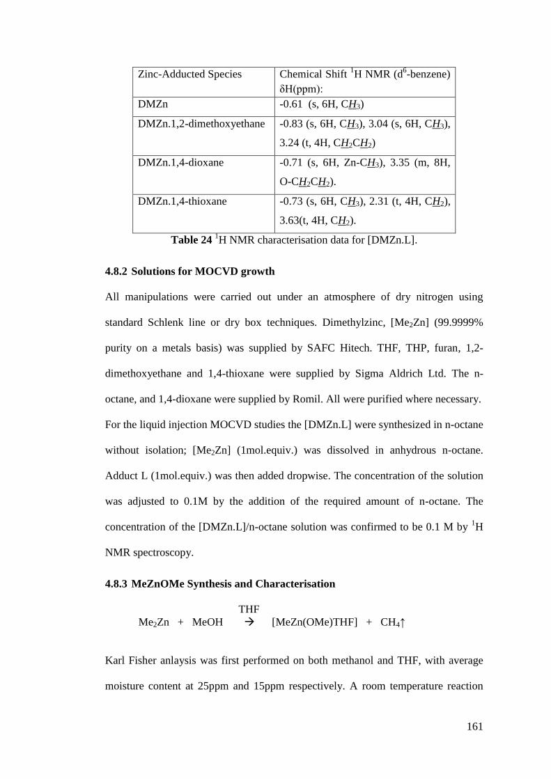
161
Zinc-Adducted Species Chemical Shift 1H NMR (d
6-benzene)
δH(ppm):
DMZn -0.61 (s, 6H, CH3)
DMZn.1,2-dimethoxyethane -0.83 (s, 6H, CH3), 3.04 (s, 6H, CH3),
3.24 (t, 4H, CH2CH2)
DMZn.1,4-dioxane -0.71 (s, 6H, Zn-CH3), 3.35 (m, 8H,
O-CH2CH2).
DMZn.1,4-thioxane -0.73 (s, 6H, CH3), 2.31 (t, 4H, CH2),
3.63(t, 4H, CH2).
Table 24 1H NMR characterisation data for [DMZn.L].
4.8.2 Solutions for MOCVD growth
All manipulations were carried out under an atmosphere of dry nitrogen using
standard Schlenk line or dry box techniques. Dimethylzinc, [Me2Zn] (99.9999%
purity on a metals basis) was supplied by SAFC Hitech. THF, THP, furan, 1,2-
dimethoxyethane and 1,4-thioxane were supplied by Sigma Aldrich Ltd. The n-
octane, and 1,4-dioxane were supplied by Romil. All were purified where necessary.
For the liquid injection MOCVD studies the [DMZn.L] were synthesized in n-octane
without isolation; [Me2Zn] (1mol.equiv.) was dissolved in anhydrous n-octane.
Adduct L (1mol.equiv.) was then added dropwise. The concentration of the solution
was adjusted to 0.1M by the addition of the required amount of n-octane. The
concentration of the [DMZn.L]/n-octane solution was confirmed to be 0.1 M by 1H
NMR spectroscopy.
4.8.3 MeZnOMe Synthesis and Characterisation
THF
Me2Zn + MeOH [MeZn(OMe)THF] + CH4↑
Karl Fisher anlaysis was first performed on both methanol and THF, with average
moisture content at 25ppm and 15ppm respectively. A room temperature reaction
162
was carried out using standard Schlenk line techniques. Me2Zn (10.4g, 0.109mol)
was solvated in THF (25ml) in glovebox. MeOH (5.3ml, 0.109mol) was solvated in
THF (25ml). The MeOH/THF mixture was added to Me2Zn/THF slowly with
stirring, with a total addition time of 45mins. On addition, vigorous bubbling and
strong exothermic reaction observed. As addition continued, white precipitate began
to form. The clear solution was filtered away from the white precipitate.
This same method was repeated at a reduced temperature of approx. -40ºC. This was
to confirm that disproportionation doesn't occur at a higher temperature. Both
reaction products were analysed by 1H NMR using d
6-benzene as a reference. :
-0.41 (s, 18 H; ZnCH3), 3.37(s, 18 H; OCH3), 3.40 ppm (s, 6H; OCH3) .
163
Chapter 5 Copper Results and Discussion
5.1 Overview
This chapter examines the investigation into the deposition of Cu2O. As discussed
previously, Cu2O is a p-type oxide and is the target material to form a p-n junction
with ZnO. In addition, the scope of this investigation enabled the deposition of
metallic copper to be studied. This is of interest in its own right as a metallisation
layer for electronic devices and was highlighted in section 2.2.
For deposition work involving copper, two precursors were investigated, a Cu(I) β-
diketonate, copper hexafluroacetylacetanato cyclo-octadiene, Cu(hfac)(COD) and a
Cu(I) complex namely, cyclopentadienyl copper tertiary butyl isocyanide,
CpCu(tBuNC). Cu(hfac)(COD), shown in Figure 82 was trialled first in a liquid
injection method via thermal decomposition, CVD, and via ALD with both tertiary
butyl hydrazine and ozone as co-reagents. With this precursor the deposition of Cu
and CuO layers was achieved. Synthesis and the deposition parameters investigated
are summarised in section 5.6.
Figure 82 Cu(hfac)(COD).
As the target layer for the PV device was Cu2O, a further precursor, CpCu(tBuNC),
was studied via conventional and plasma enhanced ALD. This target molecule was
chosen as a potential ALD precursor due to its previous use in CVD.202, 305
Figure
83 identifies the synthesis route, and the molecule 306, 307
with further experimental
details provided in section 5.6.
164
Figure 83 Reaction scheme for the synthesis of CpCu(tBuNC).
The compound was characterised by 1H NMR and the spectra is presented in Figure
84. The spectra (undertaken at an extended relaxation time of 25seconds), shows the
expected singlet resonances at δ= 0.5ppm and δ= 6.2 ppm with the correct proton
ratio of 9:5 respectively, indicating an ɳ5-coordination mode of Cp to copper in the
solution phase at room temperature.
Figure 84 1H NMR with a photograph insert of CpCu(
tBuNC).
1H NMR (C6D6):
δ(ppm): -0.6ppm (s,9H,N-C(CH3)3), 6.2 (s, 5H, -C5H5)
165
The co-ordination mode of the Cp to the copper is further confirmed in the work
undertaken by Willcocks202
in which the molecular structure confirms a pseudo two-
coordinate, half sandwhich system. There is a slight deviation from full lineratity to
an angle of 173° between the Cp-Cu-C bond and an angle of 177° for the N-C-Cu
bond. This deviation is thought to be due to crystal packing effects. The Cu-
Cp(centroid) distance is 1.849Å and Cu-C distance is 1.8152Å.
The TGA for CpCu(tBuNC) is given in Figure 85. A mass drop begins at a
temperature of 100°C and extends to 175°C relating to volatilisation of the
precursor, with the the mass loss being 76.3%. From 200°C onwards there is a much
slower rate of mass loss as the species here is less volatile than the main precursor.
The plateau weight of 21.5% is less than the expected 34% which would correlate
to copper metal. This shows that volatilsation of the compound containing the
copper metal is possible.
Figure 85 TGA of CpCu(tBuNC).
The TGA curve provided an indication of the temperature required to transport the
precursor.
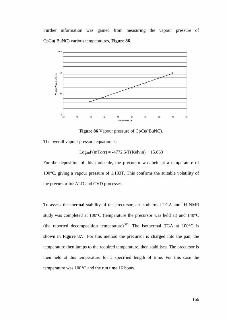
166
Further information was gained from measuring the vapour pressure of
CpCu(tBuNC) various temperatures, Figure 86.
Figure 86 Vapour pressure of CpCu(tBuNC).
The overall vapour pressure equation is:
Log10P(mTorr) = -4772.5/T(Kelvin) + 15.863
For the deposition of this molecule, the precursor was held at a temperature of
100°C, giving a vapour pressure of 1.183T. This confirms the suitable volatility of
the precursor for ALD and CVD processes.
To assess the thermal stability of the precursor, an isothermal TGA and 1H NMR
study was completed at 100°C (temperature the precursor was held at) and 140°C
(the reported decomposition temperature)305
. The isothermal TGA at 100°C is
shown in Figure 87. For this method the precursor is charged into the pan, the
temperature then jumps to the required temperature, then stabilises. The precursor is
then held at this temperature for a specified length of time. For this case the
temperature was 100°C and the run time 16 hours.
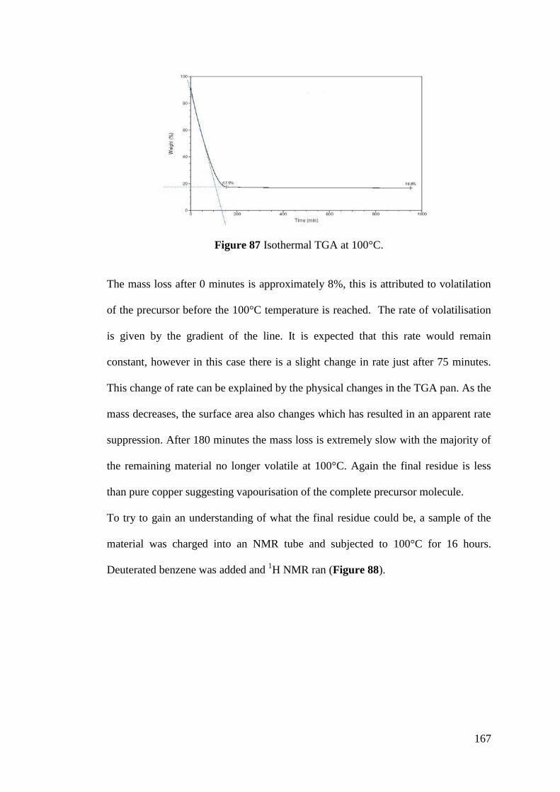
167
Figure 87 Isothermal TGA at 100°C.
The mass loss after 0 minutes is approximately 8%, this is attributed to volatilation
of the precursor before the 100°C temperature is reached. The rate of volatilisation
is given by the gradient of the line. It is expected that this rate would remain
constant, however in this case there is a slight change in rate just after 75 minutes.
This change of rate can be explained by the physical changes in the TGA pan. As the
mass decreases, the surface area also changes which has resulted in an apparent rate
suppression. After 180 minutes the mass loss is extremely slow with the majority of
the remaining material no longer volatile at 100°C. Again the final residue is less
than pure copper suggesting vapourisation of the complete precursor molecule.
To try to gain an understanding of what the final residue could be, a sample of the
material was charged into an NMR tube and subjected to 100°C for 16 hours.
Deuterated benzene was added and 1H NMR ran (Figure 88).
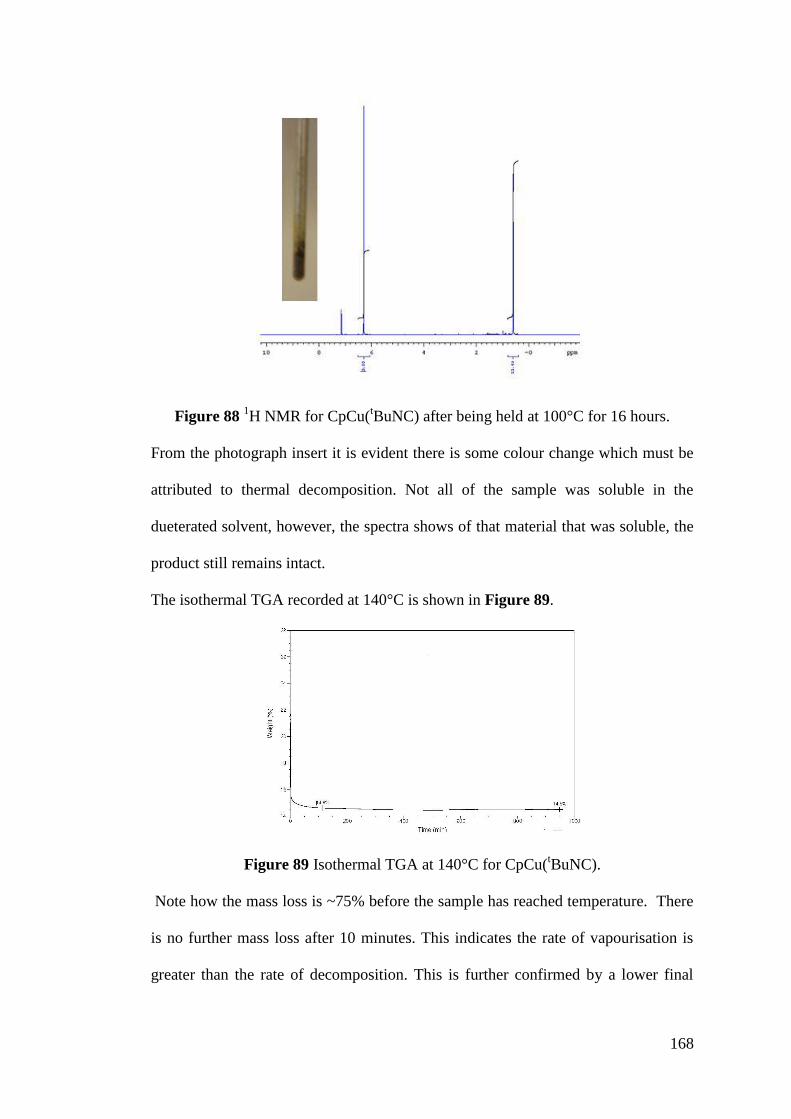
168
Figure 88 1H NMR for CpCu(
tBuNC) after being held at 100°C for 16 hours.
From the photograph insert it is evident there is some colour change which must be
attributed to thermal decomposition. Not all of the sample was soluble in the
dueterated solvent, however, the spectra shows of that material that was soluble, the
product still remains intact.
The isothermal TGA recorded at 140°C is shown in Figure 89.
Figure 89 Isothermal TGA at 140°C for CpCu(tBuNC).
Note how the mass loss is ~75% before the sample has reached temperature. There
is no further mass loss after 10 minutes. This indicates the rate of vapourisation is
greater than the rate of decomposition. This is further confirmed by a lower final
169
residue of 14.5%. On completing a similar thermal NMR study to that at 100°C, the
thermal decomposition was more evident with the sample much darker in colour. On
running the NMR for this sample, very little was soluble. The 2% final residue
difference for the isothermal samples at 100°C vs 140°C could account for the
soluble material.
Thin film growth was trialled with CpCu(tBuNC) in the following 5 schemes:
Thermal decomposition with no co-reactant
ALD with water co-reagent
ALD with O2 plasma co-reagent
ALD with H2 plasma co-reagent
ALD with táertiary butyl hydrazine co-reagent
Both thermal decomposition and using H2 plasma as a co-reagent gave metallic
copper films, whilst, water and O2 plasma gave Cu2O and CuO respectively. With
tertiary butyl hydrazine no growth was observed. In the following sections each
growth regime will be discussed with regards to growth rates and temperature
dependence, followed subsequently with characterisation, including comparisons, of
the film and material characteristics achieved with each deposition system.
5.2 Deposition of Metallic Copper Films
5.2.1 Thermal Decomposition
In this section we compare the thermal decomposition of Cu(hfac)(COD) and
CpCu(tBuNC) in the absence of a co-reagent. This approach will enable a baseline
for the decomposition of both precursors to be established as a function of
temperature and to highlight the onset of CVD-like growth. Copper films from both
precursors were deposited onto silicon and borosilicate glass substrates. For the
Cu(hfac)(COD) precursor, a liquid injection methodology was employed. The
copper compound was dissolved in toluene to give a solution of 0.65M. The
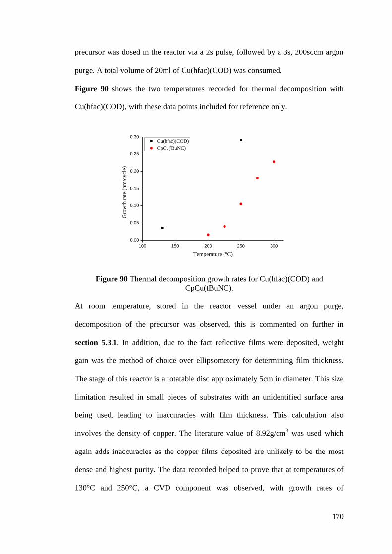
170
precursor was dosed in the reactor via a 2s pulse, followed by a 3s, 200sccm argon
purge. A total volume of 20ml of Cu(hfac)(COD) was consumed.
Figure 90 shows the two temperatures recorded for thermal decomposition with
Cu(hfac)(COD), with these data points included for reference only.
100 150 200 250 300
0.00
0.05
0.10
0.15
0.20
0.25
0.30Cu(hfac)(COD)
CpCu(tBuNC)
Gro
wth
rat
e (n
m/c
ycl
e)
Temperature (°C)
Figure 90 Thermal decomposition growth rates for Cu(hfac)(COD) and
CpCu(tBuNC).
At room temperature, stored in the reactor vessel under an argon purge,
decomposition of the precursor was observed, this is commented on further in
section 5.3.1. In addition, due to the fact reflective films were deposited, weight
gain was the method of choice over ellipsometery for determining film thickness.
The stage of this reactor is a rotatable disc approximately 5cm in diameter. This size
limitation resulted in small pieces of substrates with an unidentified surface area
being used, leading to inaccuracies with film thickness. This calculation also
involves the density of copper. The literature value of 8.92g/cm3 was used which
again adds inaccuracies as the copper films deposited are unlikely to be the most
dense and highest purity. The data recorded helped to prove that at temperatures of
130°C and 250°C, a CVD component was observed, with growth rates of
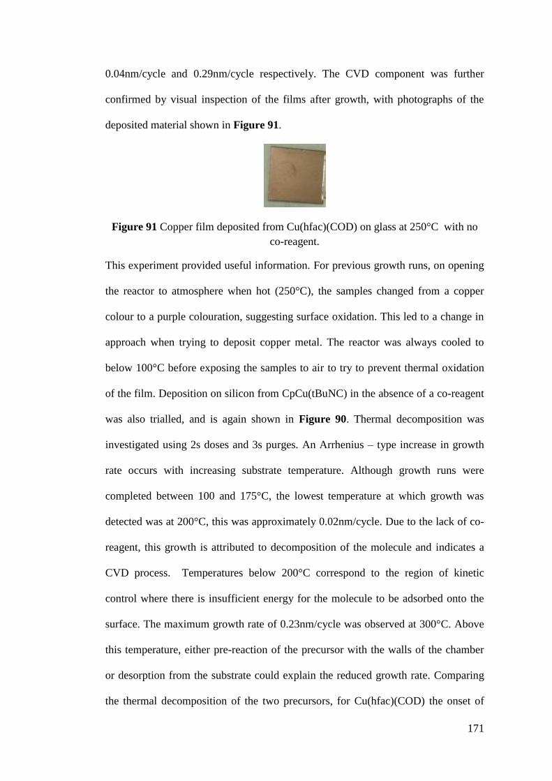
171
0.04nm/cycle and 0.29nm/cycle respectively. The CVD component was further
confirmed by visual inspection of the films after growth, with photographs of the
deposited material shown in Figure 91.
Figure 91 Copper film deposited from Cu(hfac)(COD) on glass at 250°C with no
co-reagent.
This experiment provided useful information. For previous growth runs, on opening
the reactor to atmosphere when hot (250°C), the samples changed from a copper
colour to a purple colouration, suggesting surface oxidation. This led to a change in
approach when trying to deposit copper metal. The reactor was always cooled to
below 100°C before exposing the samples to air to try to prevent thermal oxidation
of the film. Deposition on silicon from CpCu(tBuNC) in the absence of a co-reagent
was also trialled, and is again shown in Figure 90. Thermal decomposition was
investigated using 2s doses and 3s purges. An Arrhenius – type increase in growth
rate occurs with increasing substrate temperature. Although growth runs were
completed between 100 and 175°C, the lowest temperature at which growth was
detected was at 200°C, this was approximately 0.02nm/cycle. Due to the lack of co-
reagent, this growth is attributed to decomposition of the molecule and indicates a
CVD process. Temperatures below 200°C correspond to the region of kinetic
control where there is insufficient energy for the molecule to be adsorbed onto the
surface. The maximum growth rate of 0.23nm/cycle was observed at 300°C. Above
this temperature, either pre-reaction of the precursor with the walls of the chamber
or desorption from the substrate could explain the reduced growth rate. Comparing
the thermal decomposition of the two precursors, for Cu(hfac)(COD) the onset of
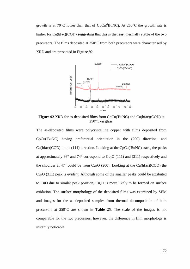
172
growth is at 70°C lower than that of CpCu(tBuNC). At 250°C the growth rate is
higher for Cu(hfac)(COD) suggesting that this is the least thermally stable of the two
precursors. The films deposited at 250°C from both precursors were characterised by
XRD and are presented in Figure 92.
30 35 40 45 50 55 60 65 70 75 80
Cu(hfac)(COD)
CpCu(tBuNC)
Cu2O(200)
Cu2O(311)
Cu2O(111) Cu(220)
Cu(200)
Inte
nsity (
Arb
. U
nits)
2 theta
Cu(III)
Figure 92 XRD for as-deposited films from CpCu(
tBuNC) and Cu(hfac)(COD) at
250°C on glass.
The as-deposited films were polycrystalline copper with films deposited from
CpCu(tBuNC) having preferential orientation in the (200) direction, and
Cu(hfac)(COD) in the (111) direction. Looking at the CpCu(tBuNC) trace, the peaks
at approximately 36° and 74° correspond to Cu2O (111) and (311) respectively and
the shoulder at 47° could be from Cu2O (200). Looking at the Cu(hfac)(COD) the
Cu2O (311) peak is evident. Although some of the smaller peaks could be attributed
to CuO due to similar peak position, Cu2O is more likely to be formed on surface
oxidation. The surface morphology of the deposited films was examined by SEM
and images for the as deposited samples from thermal decomposition of both
precursors at 250°C are shown in Table 25. The scale of the images is not
comparable for the two precursors, however, the difference in film morphology is
instantly noticable.
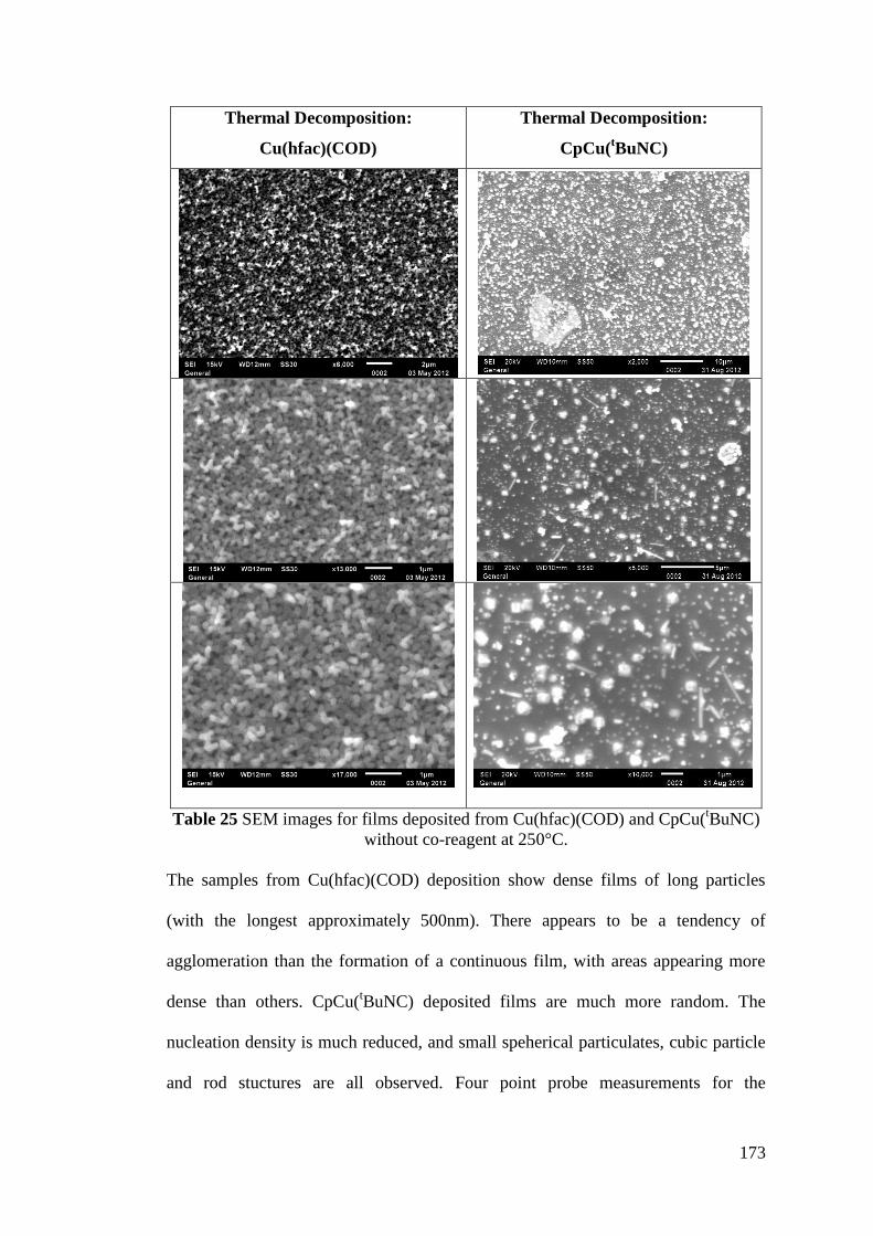
173
Thermal Decomposition:
Cu(hfac)(COD)
Thermal Decomposition:
CpCu(tBuNC)
Table 25 SEM images for films deposited from Cu(hfac)(COD) and CpCu(tBuNC)
without co-reagent at 250°C.
The samples from Cu(hfac)(COD) deposition show dense films of long particles
(with the longest approximately 500nm). There appears to be a tendency of
agglomeration than the formation of a continuous film, with areas appearing more
dense than others. CpCu(tBuNC) deposited films are much more random. The
nucleation density is much reduced, and small speherical particulates, cubic particle
and rod stuctures are all observed. Four point probe measurements for the
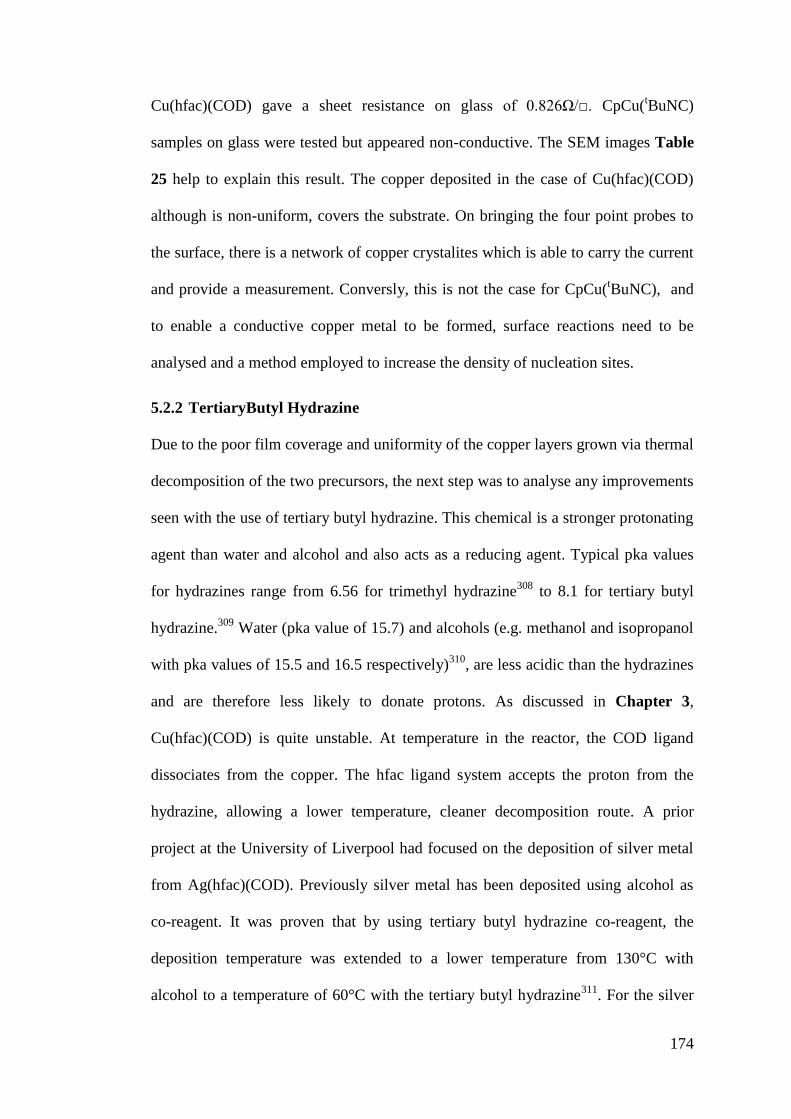
174
Cu(hfac)(COD) gave a sheet resistance on glass of 0.826Ω/. CpCu(tBuNC)
samples on glass were tested but appeared non-conductive. The SEM images Table
25 help to explain this result. The copper deposited in the case of Cu(hfac)(COD)
although is non-uniform, covers the substrate. On bringing the four point probes to
the surface, there is a network of copper crystalites which is able to carry the current
and provide a measurement. Conversly, this is not the case for CpCu(tBuNC), and
to enable a conductive copper metal to be formed, surface reactions need to be
analysed and a method employed to increase the density of nucleation sites.
5.2.2 TertiaryButyl Hydrazine
Due to the poor film coverage and uniformity of the copper layers grown via thermal
decomposition of the two precursors, the next step was to analyse any improvements
seen with the use of tertiary butyl hydrazine. This chemical is a stronger protonating
agent than water and alcohol and also acts as a reducing agent. Typical pka values
for hydrazines range from 6.56 for trimethyl hydrazine308
to 8.1 for tertiary butyl
hydrazine.309
Water (pka value of 15.7) and alcohols (e.g. methanol and isopropanol
with pka values of 15.5 and 16.5 respectively)310
, are less acidic than the hydrazines
and are therefore less likely to donate protons. As discussed in Chapter 3,
Cu(hfac)(COD) is quite unstable. At temperature in the reactor, the COD ligand
dissociates from the copper. The hfac ligand system accepts the proton from the
hydrazine, allowing a lower temperature, cleaner decomposition route. A prior
project at the University of Liverpool had focused on the deposition of silver metal
from Ag(hfac)(COD). Previously silver metal has been deposited using alcohol as
co-reagent. It was proven that by using tertiary butyl hydrazine co-reagent, the
deposition temperature was extended to a lower temperature from 130°C with
alcohol to a temperature of 60°C with the tertiary butyl hydrazine311
. For the silver
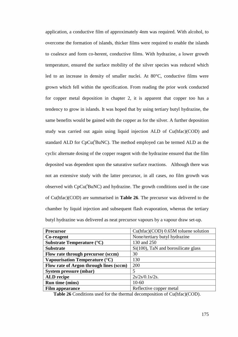
175
application, a conductive film of approximately 4nm was required. With alcohol, to
overcome the formation of islands, thicker films were required to enable the islands
to coalesce and form co-herent, conductive films. With hydrazine, a lower growth
temperature, ensured the surface mobility of the silver species was reduced which
led to an increase in density of smaller nuclei. At 80°C, conductive films were
grown which fell within the specification. From reading the prior work conducted
for copper metal deposition in chapter 2, it is apparent that copper too has a
tendency to grow in islands. It was hoped that by using tertiary butyl hydrazine, the
same benefits would be gained with the copper as for the silver. A further deposition
study was carried out again using liquid injection ALD of Cu(hfac)(COD) and
standard ALD for CpCu(tBuNC). The method employed can be termed ALD as the
cyclic alternate dosing of the copper reagent with the hydrazine ensured that the film
deposited was dependent upon the saturative surface reactions. Although there was
not an extensive study with the latter precursor, in all cases, no film growth was
observed with CpCu(tBuNC) and hydrazine. The growth conditions used in the case
of Cu(hfac)(COD) are summarised in Table 26. The precursor was delivered to the
chamber by liquid injection and subsequent flash evaporation, whereas the tertiary
butyl hydrazine was delivered as neat precursor vapours by a vapour draw set-up.
Precursor Cu(hfac)(COD) 0.65M toluene solution
Co-reagent None/tertiary butyl hydrazine
Substrate Temperature (°C) 130 and 250
Substrate Si(100), TaN and borosilicate glass
Flow rate through precursor (sccm) 30
Vapourisation Temperature (°C) 130
Flow rate of Argon through lines (sccm) 200
System pressure (mbar) 5
ALD recipe 2s/2s/0.1s/2s.
Run time (mins) 10-60
Film appearance Reflective copper metal
Table 26 Conditions used for the thermal decomposition of Cu(hfac)(COD).
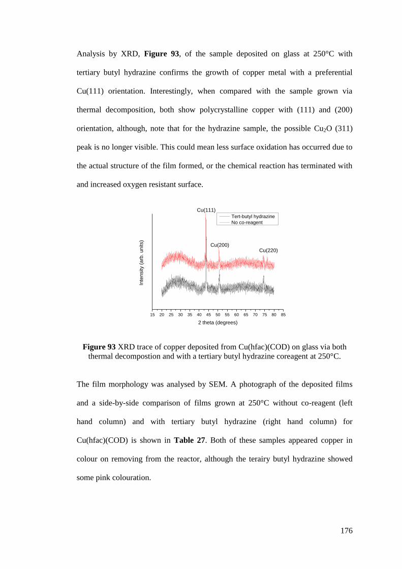
176
Analysis by XRD, Figure 93, of the sample deposited on glass at 250°C with
tertiary butyl hydrazine confirms the growth of copper metal with a preferential
Cu(111) orientation. Interestingly, when compared with the sample grown via
thermal decomposition, both show polycrystalline copper with (111) and (200)
orientation, although, note that for the hydrazine sample, the possible Cu2O (311)
peak is no longer visible. This could mean less surface oxidation has occurred due to
the actual structure of the film formed, or the chemical reaction has terminated with
and increased oxygen resistant surface.
15 20 25 30 35 40 45 50 55 60 65 70 75 80 85
Cu(220)Cu(200)
Inte
nsity (
arb
. un
its)
2 theta (degrees)
Tert-butyl hydrazine
No co-reagent
Cu(111)
Figure 93 XRD trace of copper deposited from Cu(hfac)(COD) on glass via both
thermal decompostion and with a tertiary butyl hydrazine coreagent at 250°C.
The film morphology was analysed by SEM. A photograph of the deposited films
and a side-by-side comparison of films grown at 250°C without co-reagent (left
hand column) and with tertiary butyl hydrazine (right hand column) for
Cu(hfac)(COD) is shown in Table 27. Both of these samples appeared copper in
colour on removing from the reactor, although the terairy butyl hydrazine showed
some pink colouration.
177
Thermal Decomposition ALD with tertiary butyl hydrazine
250°C, 20ml precursor consumed, T=174Å 250°C, 20ml precursor consumed,
325cyles of 2s/2s/0.1s/2s. T=240 Å
Table 27 SEM images for films deposited using Cu(hfac)(COD) via thermal
decomposition and with tertiary butyl hydrazine co-reagent on Si(100) at 250°C.
There is an increased growth rate observed when the more reactive tertiary butyl
hydrazine is used. Note also that there is change in particle shape, for the thermal
decomposition sample they appear more ‘worm-like’ whilst for the samples
deposited with tertiary butyl hydrazine, they appear much more spherical. Looking
more closely, the right hand side column also appears to show smaller particles
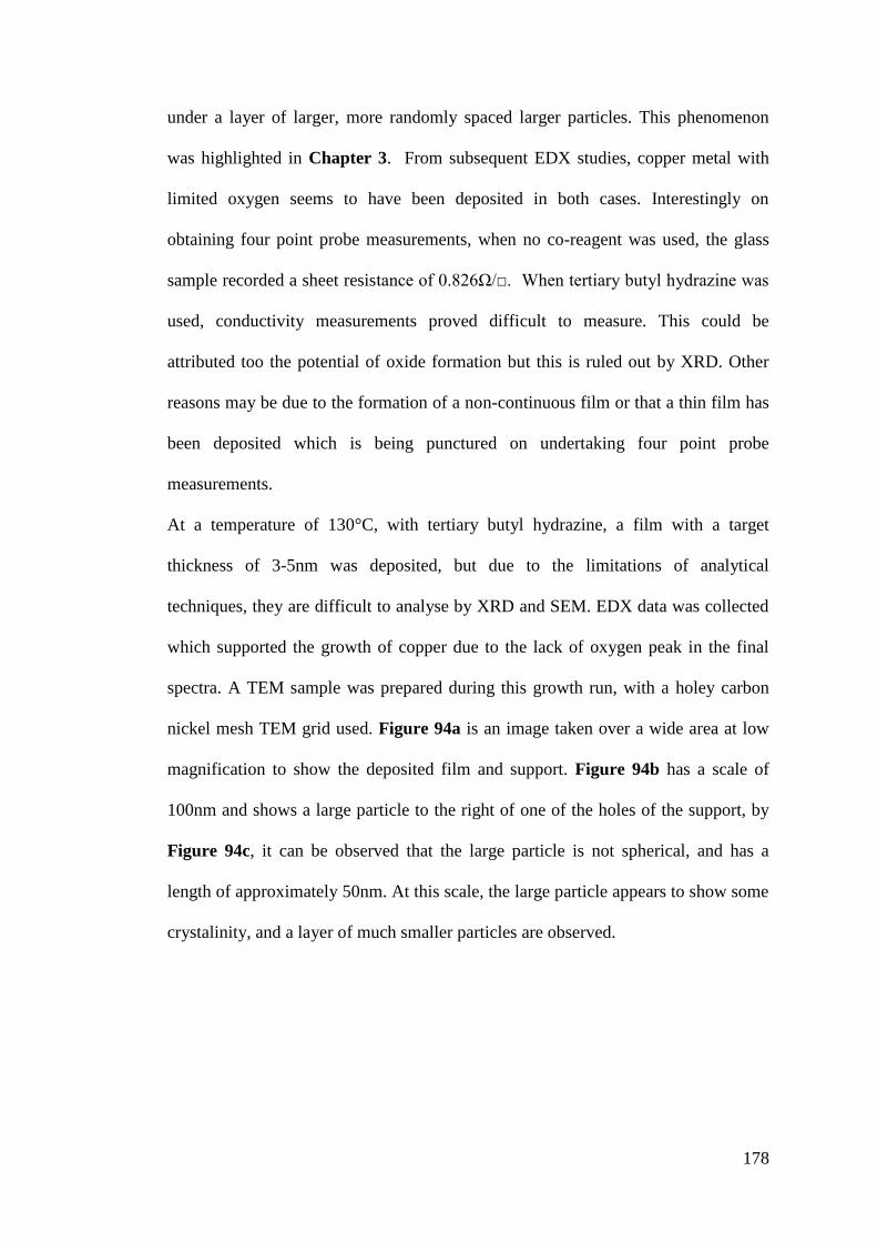
178
under a layer of larger, more randomly spaced larger particles. This phenomenon
was highlighted in Chapter 3. From subsequent EDX studies, copper metal with
limited oxygen seems to have been deposited in both cases. Interestingly on
obtaining four point probe measurements, when no co-reagent was used, the glass
sample recorded a sheet resistance of 0.826Ω/. When tertiary butyl hydrazine was
used, conductivity measurements proved difficult to measure. This could be
attributed too the potential of oxide formation but this is ruled out by XRD. Other
reasons may be due to the formation of a non-continuous film or that a thin film has
been deposited which is being punctured on undertaking four point probe
measurements.
At a temperature of 130°C, with tertiary butyl hydrazine, a film with a target
thickness of 3-5nm was deposited, but due to the limitations of analytical
techniques, they are difficult to analyse by XRD and SEM. EDX data was collected
which supported the growth of copper due to the lack of oxygen peak in the final
spectra. A TEM sample was prepared during this growth run, with a holey carbon
nickel mesh TEM grid used. Figure 94a is an image taken over a wide area at low
magnification to show the deposited film and support. Figure 94b has a scale of
100nm and shows a large particle to the right of one of the holes of the support, by
Figure 94c, it can be observed that the large particle is not spherical, and has a
length of approximately 50nm. At this scale, the large particle appears to show some
crystalinity, and a layer of much smaller particles are observed.
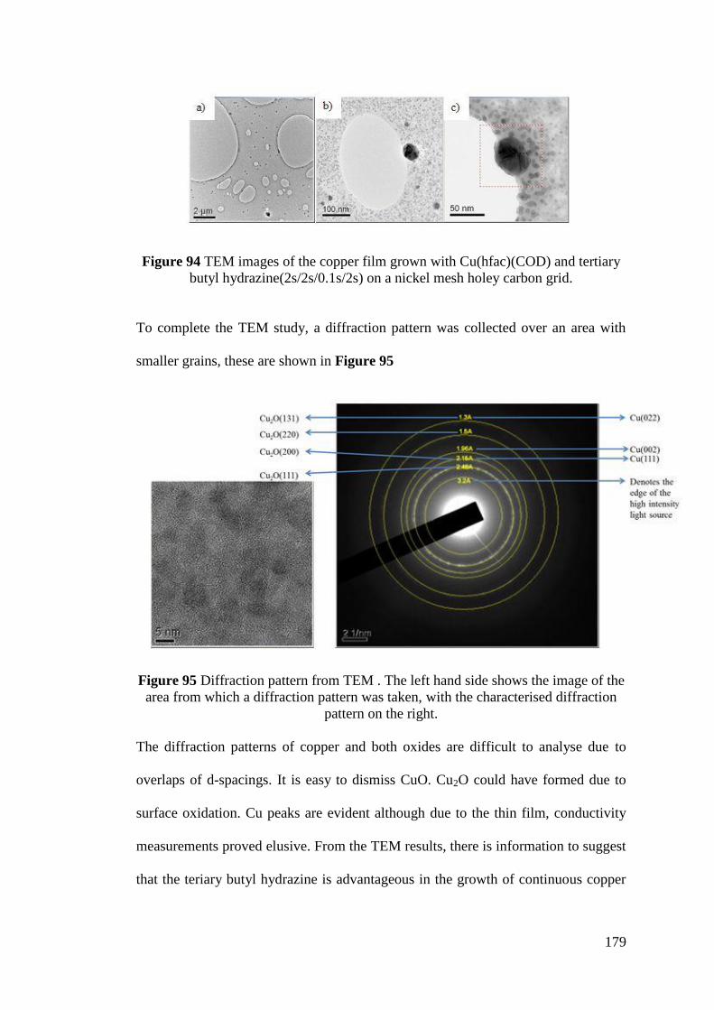
179
Figure 94 TEM images of the copper film grown with Cu(hfac)(COD) and tertiary
butyl hydrazine(2s/2s/0.1s/2s) on a nickel mesh holey carbon grid.
To complete the TEM study, a diffraction pattern was collected over an area with
smaller grains, these are shown in Figure 95
Figure 95 Diffraction pattern from TEM . The left hand side shows the image of the
area from which a diffraction pattern was taken, with the characterised diffraction
pattern on the right.
The diffraction patterns of copper and both oxides are difficult to analyse due to
overlaps of d-spacings. It is easy to dismiss CuO. Cu2O could have formed due to
surface oxidation. Cu peaks are evident although due to the thin film, conductivity
measurements proved elusive. From the TEM results, there is information to suggest
that the teriary butyl hydrazine is advantageous in the growth of continuous copper
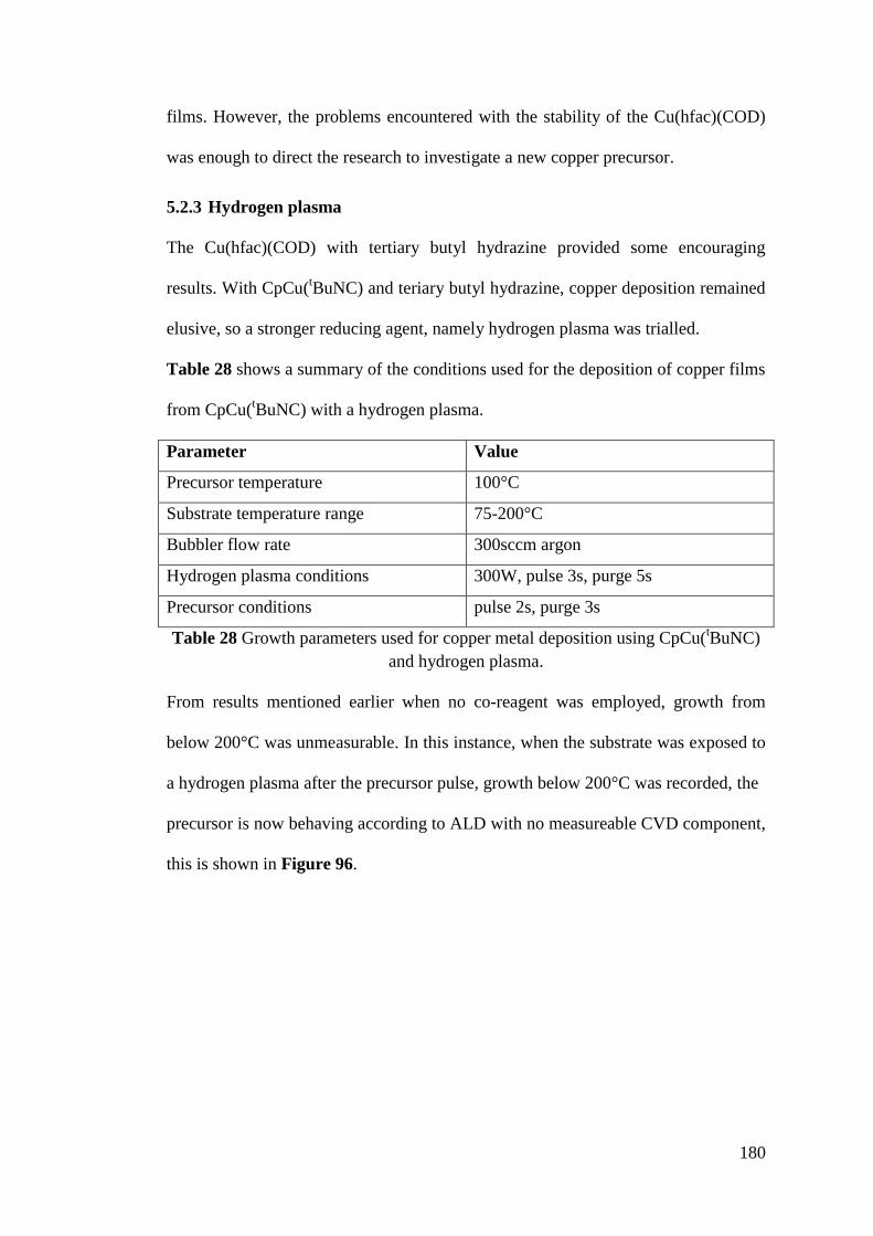
180
films. However, the problems encountered with the stability of the Cu(hfac)(COD)
was enough to direct the research to investigate a new copper precursor.
5.2.3 Hydrogen plasma
The Cu(hfac)(COD) with tertiary butyl hydrazine provided some encouraging
results. With CpCu(tBuNC) and teriary butyl hydrazine, copper deposition remained
elusive, so a stronger reducing agent, namely hydrogen plasma was trialled.
Table 28 shows a summary of the conditions used for the deposition of copper films
from CpCu(tBuNC) with a hydrogen plasma.
Parameter Value
Precursor temperature 100°C
Substrate temperature range 75-200°C
Bubbler flow rate 300sccm argon
Hydrogen plasma conditions 300W, pulse 3s, purge 5s
Precursor conditions pulse 2s, purge 3s
Table 28 Growth parameters used for copper metal deposition using CpCu(tBuNC)
and hydrogen plasma.
From results mentioned earlier when no co-reagent was employed, growth from
below 200°C was unmeasurable. In this instance, when the substrate was exposed to
a hydrogen plasma after the precursor pulse, growth below 200°C was recorded, the
precursor is now behaving according to ALD with no measureable CVD component,
this is shown in Figure 96.
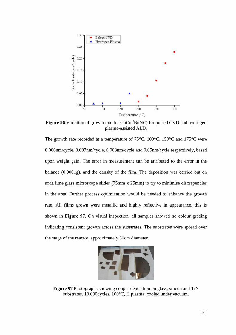
181
Figure 96 Variation of growth rate for CpCu(
tBuNC) for pulsed CVD and hydrogen
plasma-assisted ALD.
The growth rate recorded at a temperature of 75°C, 100°C, 150°C and 175°C were
0.006nm/cycle, 0.007nm/cycle, 0.008nm/cycle and 0.05nm/cycle respectively, based
upon weight gain. The error in measurement can be attributed to the error in the
balance (0.0001g), and the density of the film. The deposition was carried out on
soda lime glass microscope slides (75mm x 25mm) to try to minimise discrepencies
in the area. Further process optimization would be needed to enhance the growth
rate. All films grown were metallic and highly reflective in appearance, this is
shown in Figure 97. On visual inspection, all samples showed no colour grading
indicating consistent growth across the substrates. The substrates were spread over
the stage of the reactor, approximately 30cm diameter.
Figure 97 Photographs showing copper deposition on glass, silicon and TiN
substrates. 10,000cycles, 100°C, H plasma, cooled under vacuum.
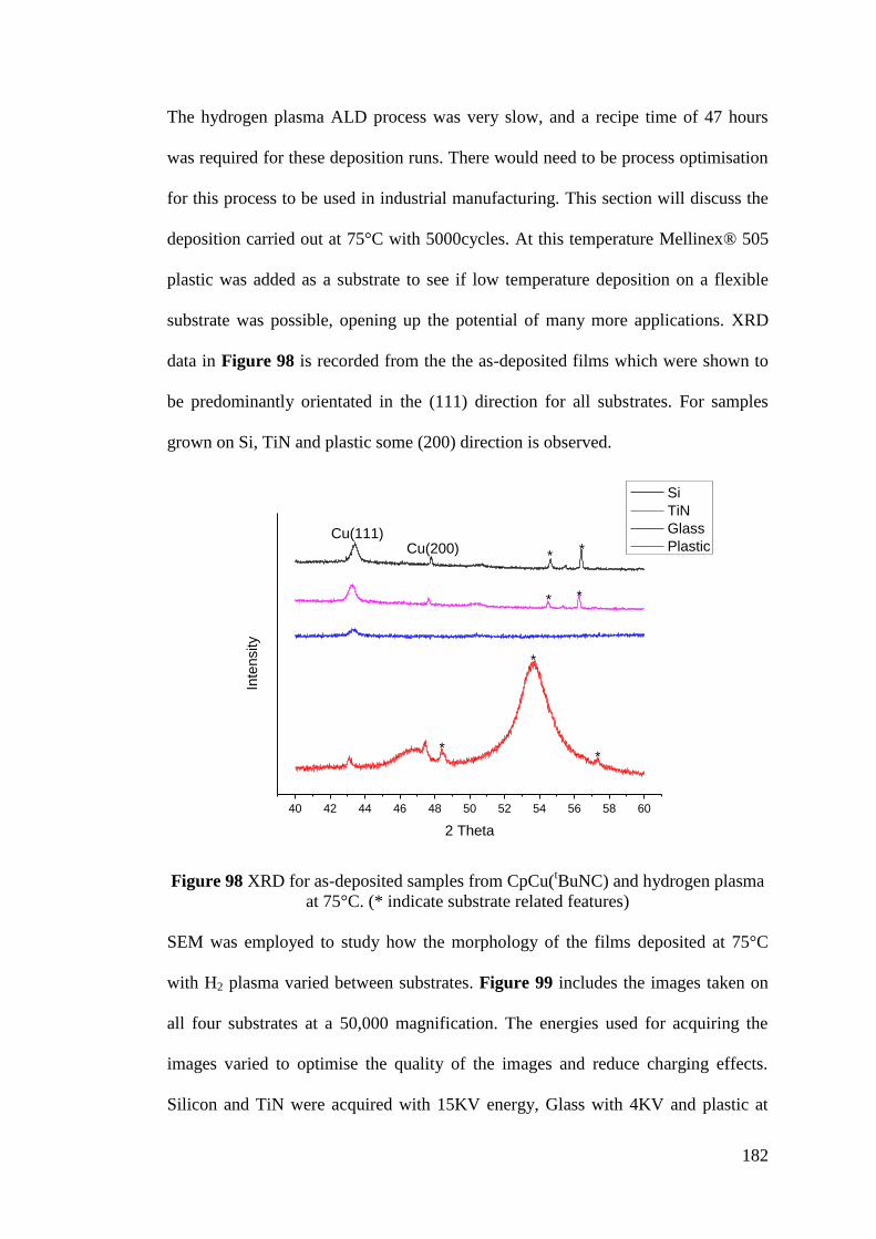
182
The hydrogen plasma ALD process was very slow, and a recipe time of 47 hours
was required for these deposition runs. There would need to be process optimisation
for this process to be used in industrial manufacturing. This section will discuss the
deposition carried out at 75°C with 5000cycles. At this temperature Mellinex® 505
plastic was added as a substrate to see if low temperature deposition on a flexible
substrate was possible, opening up the potential of many more applications. XRD
data in Figure 98 is recorded from the the as-deposited films which were shown to
be predominantly orientated in the (111) direction for all substrates. For samples
grown on Si, TiN and plastic some (200) direction is observed.
40 42 44 46 48 50 52 54 56 58 60
**
*
* *
**Cu(200)
Inte
nsity
2 Theta
Si
TiN
Glass
PlasticCu(111)
Figure 98 XRD for as-deposited samples from CpCu(tBuNC) and hydrogen plasma
at 75°C. (* indicate substrate related features)
SEM was employed to study how the morphology of the films deposited at 75°C
with H2 plasma varied between substrates. Figure 99 includes the images taken on
all four substrates at a 50,000 magnification. The energies used for acquiring the
images varied to optimise the quality of the images and reduce charging effects.
Silicon and TiN were acquired with 15KV energy, Glass with 4KV and plastic at
(111)
(200)
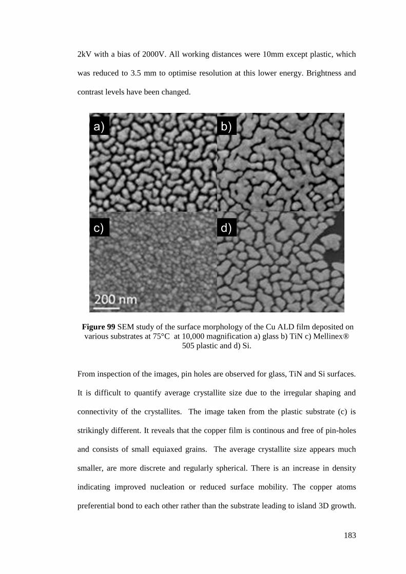
183
2kV with a bias of 2000V. All working distances were 10mm except plastic, which
was reduced to 3.5 mm to optimise resolution at this lower energy. Brightness and
contrast levels have been changed.
Figure 99 SEM study of the surface morphology of the Cu ALD film deposited on
various substrates at 75°C at 10,000 magnification a) glass b) TiN c) Mellinex®
505 plastic and d) Si.
From inspection of the images, pin holes are observed for glass, TiN and Si surfaces.
It is difficult to quantify average crystallite size due to the irregular shaping and
connectivity of the crystallites. The image taken from the plastic substrate (c) is
strikingly different. It reveals that the copper film is continous and free of pin-holes
and consists of small equiaxed grains. The average crystallite size appears much
smaller, are more discrete and regularly spherical. There is an increase in density
indicating improved nucleation or reduced surface mobility. The copper atoms
preferential bond to each other rather than the substrate leading to island 3D growth.
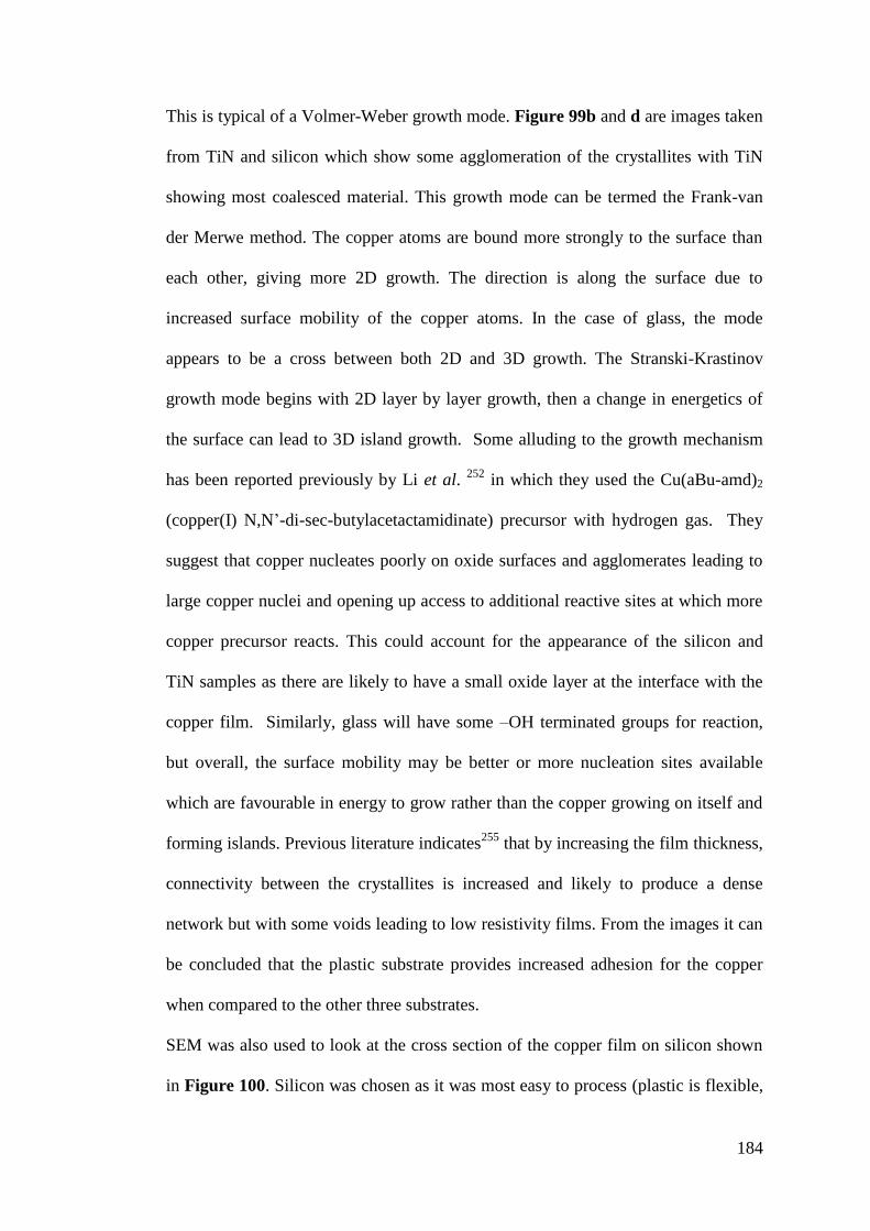
184
This is typical of a Volmer-Weber growth mode. Figure 99b and d are images taken
from TiN and silicon which show some agglomeration of the crystallites with TiN
showing most coalesced material. This growth mode can be termed the Frank-van
der Merwe method. The copper atoms are bound more strongly to the surface than
each other, giving more 2D growth. The direction is along the surface due to
increased surface mobility of the copper atoms. In the case of glass, the mode
appears to be a cross between both 2D and 3D growth. The Stranski-Krastinov
growth mode begins with 2D layer by layer growth, then a change in energetics of
the surface can lead to 3D island growth. Some alluding to the growth mechanism
has been reported previously by Li et al. 252
in which they used the Cu(aBu-amd)2
(copper(I) N,N’-di-sec-butylacetactamidinate) precursor with hydrogen gas. They
suggest that copper nucleates poorly on oxide surfaces and agglomerates leading to
large copper nuclei and opening up access to additional reactive sites at which more
copper precursor reacts. This could account for the appearance of the silicon and
TiN samples as there are likely to have a small oxide layer at the interface with the
copper film. Similarly, glass will have some –OH terminated groups for reaction,
but overall, the surface mobility may be better or more nucleation sites available
which are favourable in energy to grow rather than the copper growing on itself and
forming islands. Previous literature indicates255
that by increasing the film thickness,
connectivity between the crystallites is increased and likely to produce a dense
network but with some voids leading to low resistivity films. From the images it can
be concluded that the plastic substrate provides increased adhesion for the copper
when compared to the other three substrates.
SEM was also used to look at the cross section of the copper film on silicon shown
in Figure 100. Silicon was chosen as it was most easy to process (plastic is flexible,
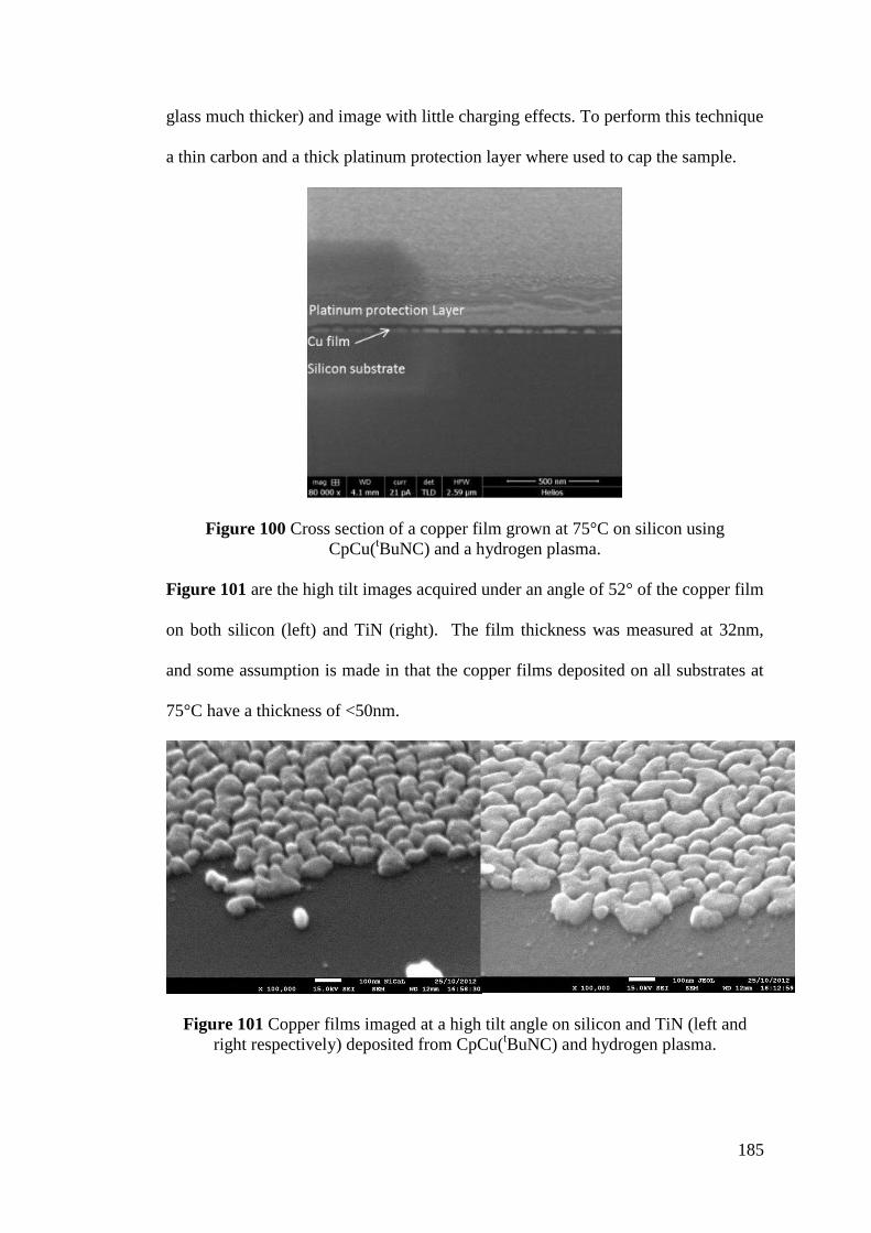
185
glass much thicker) and image with little charging effects. To perform this technique
a thin carbon and a thick platinum protection layer where used to cap the sample.
Figure 100 Cross section of a copper film grown at 75°C on silicon using
CpCu(tBuNC) and a hydrogen plasma.
Figure 101 are the high tilt images acquired under an angle of 52° of the copper film
on both silicon (left) and TiN (right). The film thickness was measured at 32nm,
and some assumption is made in that the copper films deposited on all substrates at
75°C have a thickness of <50nm.
Figure 101 Copper films imaged at a high tilt angle on silicon and TiN (left and
right respectively) deposited from CpCu(tBuNC) and hydrogen plasma.
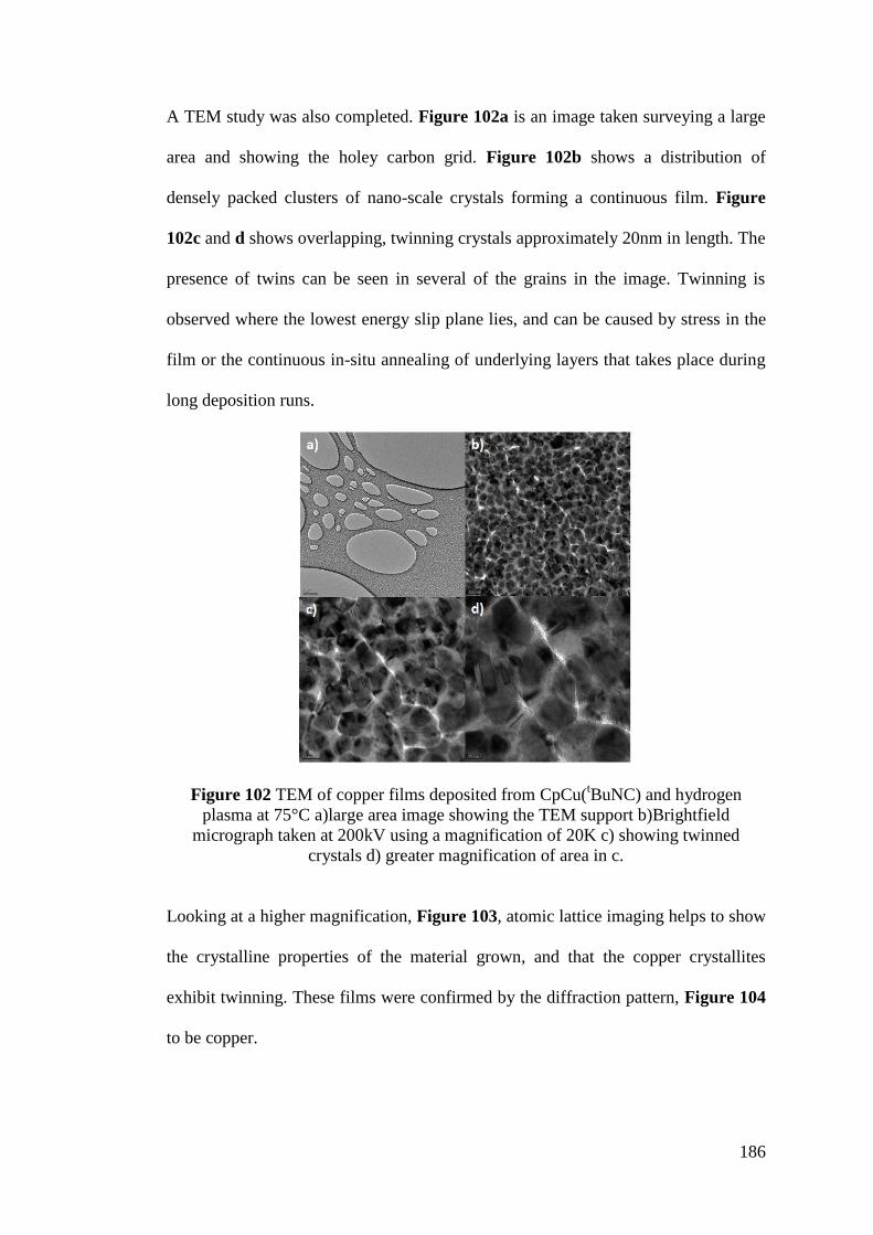
186
A TEM study was also completed. Figure 102a is an image taken surveying a large
area and showing the holey carbon grid. Figure 102b shows a distribution of
densely packed clusters of nano-scale crystals forming a continuous film. Figure
102c and d shows overlapping, twinning crystals approximately 20nm in length. The
presence of twins can be seen in several of the grains in the image. Twinning is
observed where the lowest energy slip plane lies, and can be caused by stress in the
film or the continuous in-situ annealing of underlying layers that takes place during
long deposition runs.
Figure 102 TEM of copper films deposited from CpCu(tBuNC) and hydrogen
plasma at 75°C a)large area image showing the TEM support b)Brightfield
micrograph taken at 200kV using a magnification of 20K c) showing twinned
crystals d) greater magnification of area in c.
Looking at a higher magnification, Figure 103, atomic lattice imaging helps to show
the crystalline properties of the material grown, and that the copper crystallites
exhibit twinning. These films were confirmed by the diffraction pattern, Figure 104
to be copper.
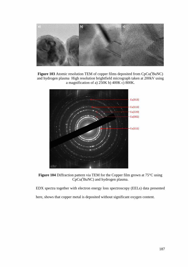
187
Figure 103 Atomic resolution TEM of copper films deposited from CpCu(tBuNC)
and hydrogen plasma High resolution brightfield micrograph taken at 200kV using
a magnification of a) 250K b) 400K c) 800K.
Figure 104 Diffraction pattern via TEM for the Copper film grown at 75°C using
CpCu(tBuNC) and hydrogen plasma.
EDX spectra together with electron energy loss spectroscopy (EELs) data presented
here, shows that copper metal is deposited without significant oxygen content.
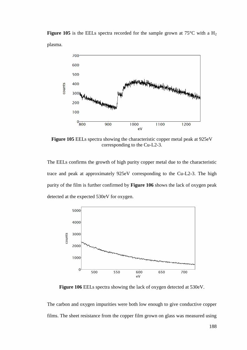
188
Figure 105 is the EELs spectra recorded for the sample grown at 75°C with a H2
plasma.
Figure 105 EELs spectra showing the characteristic copper metal peak at 925eV
corresponding to the Cu-L2-3.
The EELs confirms the growth of high purity copper metal due to the characteristic
trace and peak at approximately 925eV corresponding to the Cu-L2-3. The high
purity of the film is further confirmed by Figure 106 shows the lack of oxygen peak
detected at the expected 530eV for oxygen.
Figure 106 EELs spectra showing the lack of oxygen detected at 530eV.
The carbon and oxygen impurities were both low enough to give conductive copper
films. The sheet resistance from the copper film grown on glass was measured using
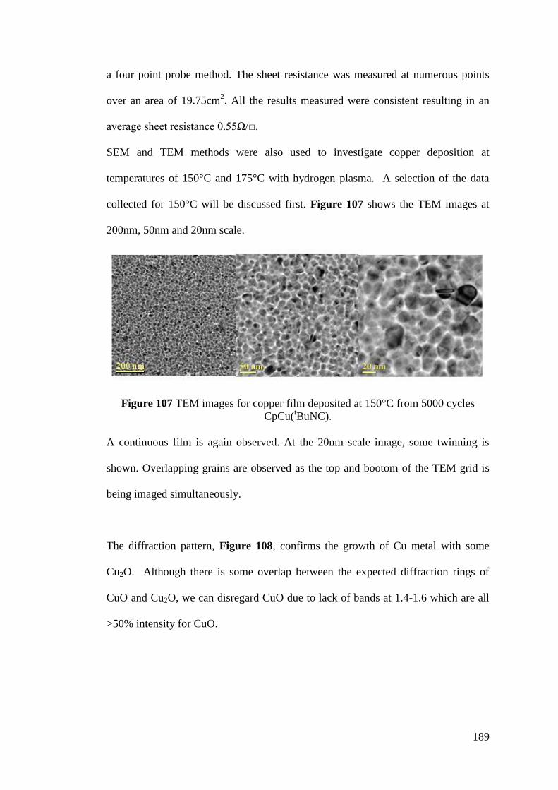
189
a four point probe method. The sheet resistance was measured at numerous points
over an area of 19.75cm2. All the results measured were consistent resulting in an
average sheet resistance 0.55Ω/.
SEM and TEM methods were also used to investigate copper deposition at
temperatures of 150°C and 175°C with hydrogen plasma. A selection of the data
collected for 150°C will be discussed first. Figure 107 shows the TEM images at
200nm, 50nm and 20nm scale.
Figure 107 TEM images for copper film deposited at 150°C from 5000 cycles
CpCu(tBuNC).
A continuous film is again observed. At the 20nm scale image, some twinning is
shown. Overlapping grains are observed as the top and bootom of the TEM grid is
being imaged simultaneously.
The diffraction pattern, Figure 108, confirms the growth of Cu metal with some
Cu2O. Although there is some overlap between the expected diffraction rings of
CuO and Cu2O, we can disregard CuO due to lack of bands at 1.4-1.6 which are all
>50% intensity for CuO.
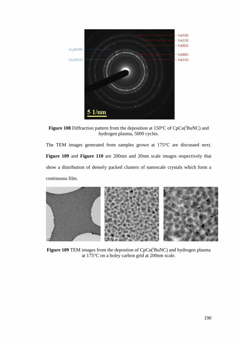
190
Figure 108 Diffraction pattern from the deposition at 150°C of CpCu(tBuNC) and
hydrogen plasma, 5000 cycles.
The TEM images generated from samples grown at 175°C are discussed next.
Figure 109 and Figure 110 are 200nm and 20nm scale images respectively that
show a distribution of densely packed clusters of nanoscale crystals which form a
continuous film.
Figure 109 TEM images from the depostion of CpCu(tBuNC) and hydrogen plasma
at 175°C on a holey carbon grid at 200nm scale.
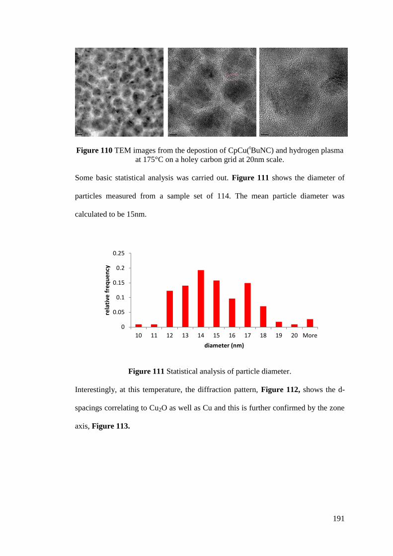
191
Figure 110 TEM images from the depostion of CpCu(tBuNC) and hydrogen plasma
at 175°C on a holey carbon grid at 20nm scale.
Some basic statistical analysis was carried out. Figure 111 shows the diameter of
particles measured from a sample set of 114. The mean particle diameter was
calculated to be 15nm.
Figure 111 Statistical analysis of particle diameter.
Interestingly, at this temperature, the diffraction pattern, Figure 112, shows the d-
spacings correlating to Cu2O as well as Cu and this is further confirmed by the zone
axis, Figure 113.
0
0.05
0.1
0.15
0.2
0.25
10 11 12 13 14 15 16 17 18 19 20 More
rela
tive
fre
qu
en
cy
diameter (nm)
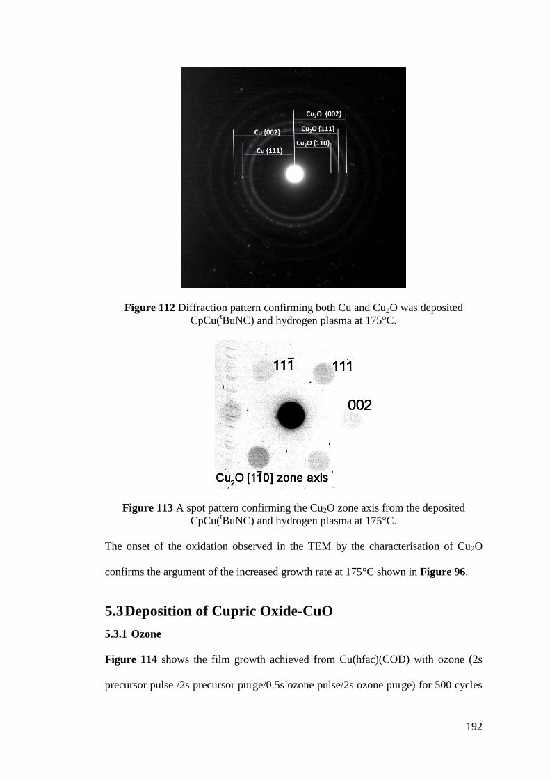
192
Figure 112 Diffraction pattern confirming both Cu and Cu2O was deposited
CpCu(tBuNC) and hydrogen plasma at 175°C.
Figure 113 A spot pattern confirming the Cu2O zone axis from the deposited
CpCu(tBuNC) and hydrogen plasma at 175°C.
The onset of the oxidation observed in the TEM by the characterisation of Cu2O
confirms the argument of the increased growth rate at 175°C shown in Figure 96.
5.3 Deposition of Cupric Oxide-CuO
5.3.1 Ozone
Figure 114 shows the film growth achieved from Cu(hfac)(COD) with ozone (2s
precursor pulse /2s precursor purge/0.5s ozone pulse/2s ozone purge) for 500 cycles
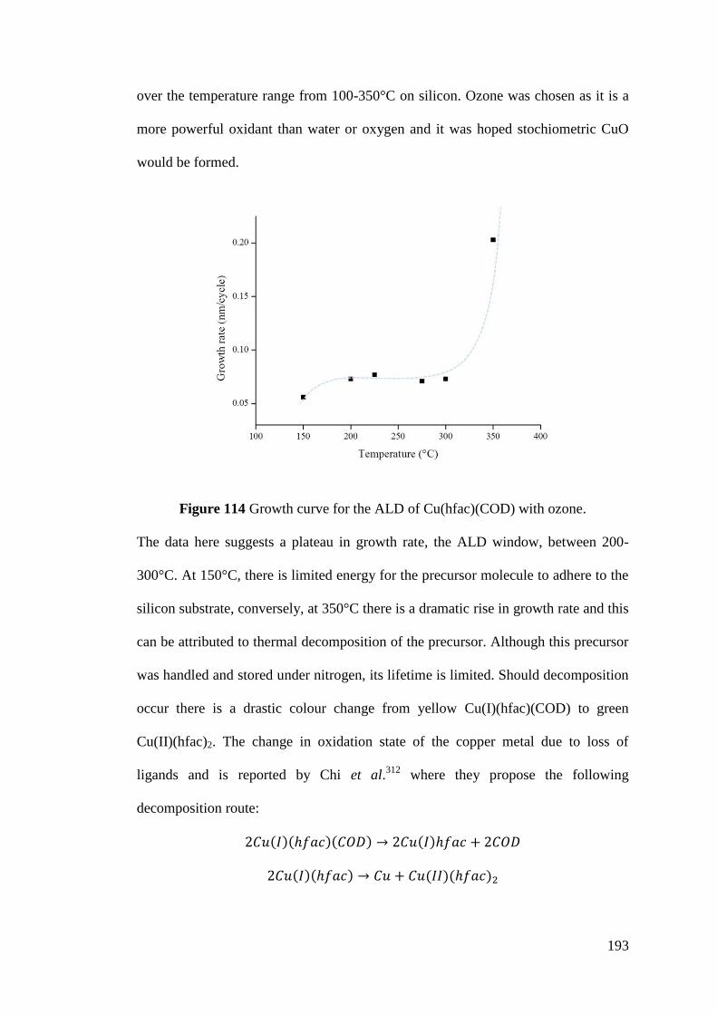
193
over the temperature range from 100-350°C on silicon. Ozone was chosen as it is a
more powerful oxidant than water or oxygen and it was hoped stochiometric CuO
would be formed.
Figure 114 Growth curve for the ALD of Cu(hfac)(COD) with ozone.
The data here suggests a plateau in growth rate, the ALD window, between 200-
300°C. At 150°C, there is limited energy for the precursor molecule to adhere to the
silicon substrate, conversely, at 350°C there is a dramatic rise in growth rate and this
can be attributed to thermal decomposition of the precursor. Although this precursor
was handled and stored under nitrogen, its lifetime is limited. Should decomposition
occur there is a drastic colour change from yellow Cu(I)(hfac)(COD) to green
Cu(II)(hfac)2. The change in oxidation state of the copper metal due to loss of
ligands and is reported by Chi et al.312
where they propose the following
decomposition route:
( )( )( ) ( )
( )( ) ( )( )
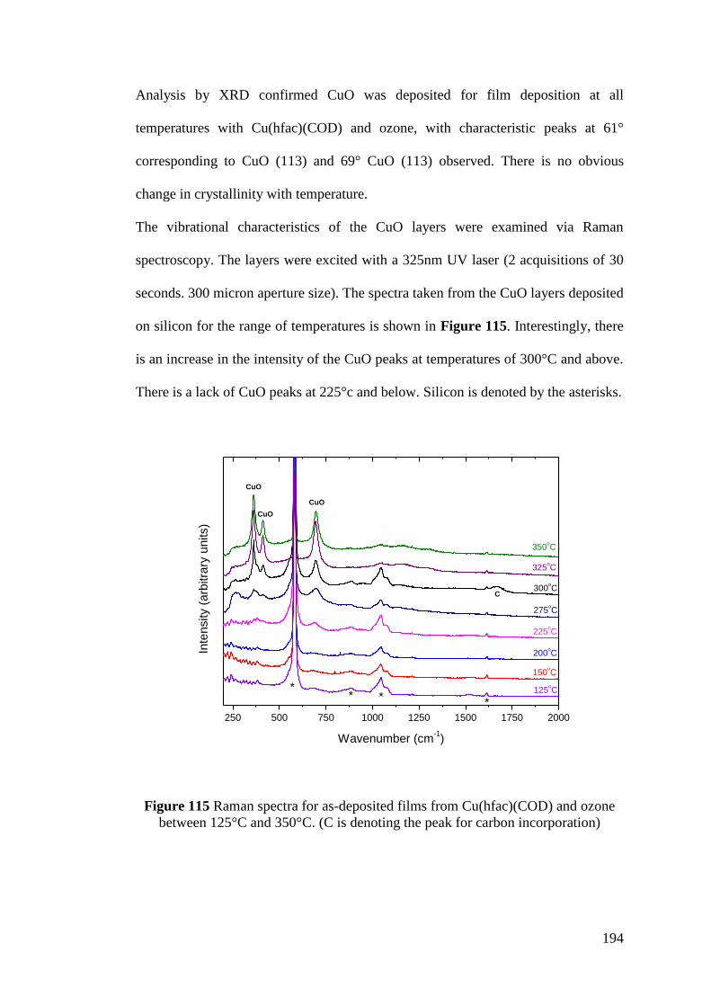
194
Analysis by XRD confirmed CuO was deposited for film deposition at all
temperatures with Cu(hfac)(COD) and ozone, with characteristic peaks at 61°
corresponding to CuO (113) and 69° CuO (113) observed. There is no obvious
change in crystallinity with temperature.
The vibrational characteristics of the CuO layers were examined via Raman
spectroscopy. The layers were excited with a 325nm UV laser (2 acquisitions of 30
seconds. 300 micron aperture size). The spectra taken from the CuO layers deposited
on silicon for the range of temperatures is shown in Figure 115. Interestingly, there
is an increase in the intensity of the CuO peaks at temperatures of 300°C and above.
There is a lack of CuO peaks at 225°c and below. Silicon is denoted by the asterisks.
250 500 750 1000 1250 1500 1750 2000
**
*
350oC
325oC
300oC
275oC
225oC
200oC
150oC
C
CuO
CuO
Inte
nsity (
arb
itra
ry u
nits)
Wavenumber (cm-1)
CuO
125oC
*
Figure 115 Raman spectra for as-deposited films from Cu(hfac)(COD) and ozone
between 125°C and 350°C. (C is denoting the peak for carbon incorporation)
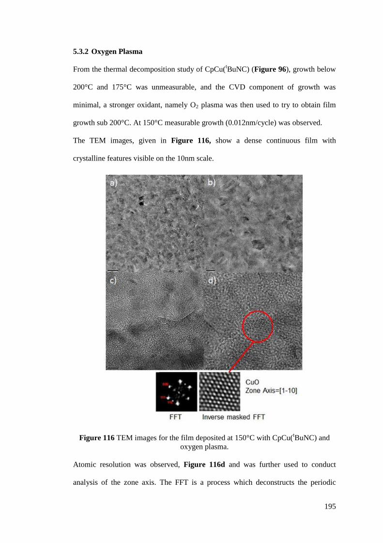
195
5.3.2 Oxygen Plasma
From the thermal decomposition study of CpCu(tBuNC) (Figure 96), growth below
200°C and 175°C was unmeasurable, and the CVD component of growth was
minimal, a stronger oxidant, namely O2 plasma was then used to try to obtain film
growth sub 200°C. At 150°C measurable growth (0.012nm/cycle) was observed.
The TEM images, given in Figure 116, show a dense continuous film with
crystalline features visible on the 10nm scale.
Figure 116 TEM images for the film deposited at 150°C with CpCu(tBuNC) and
oxygen plasma.
Atomic resolution was observed, Figure 116d and was further used to conduct
analysis of the zone axis. The FFT is a process which deconstructs the periodic
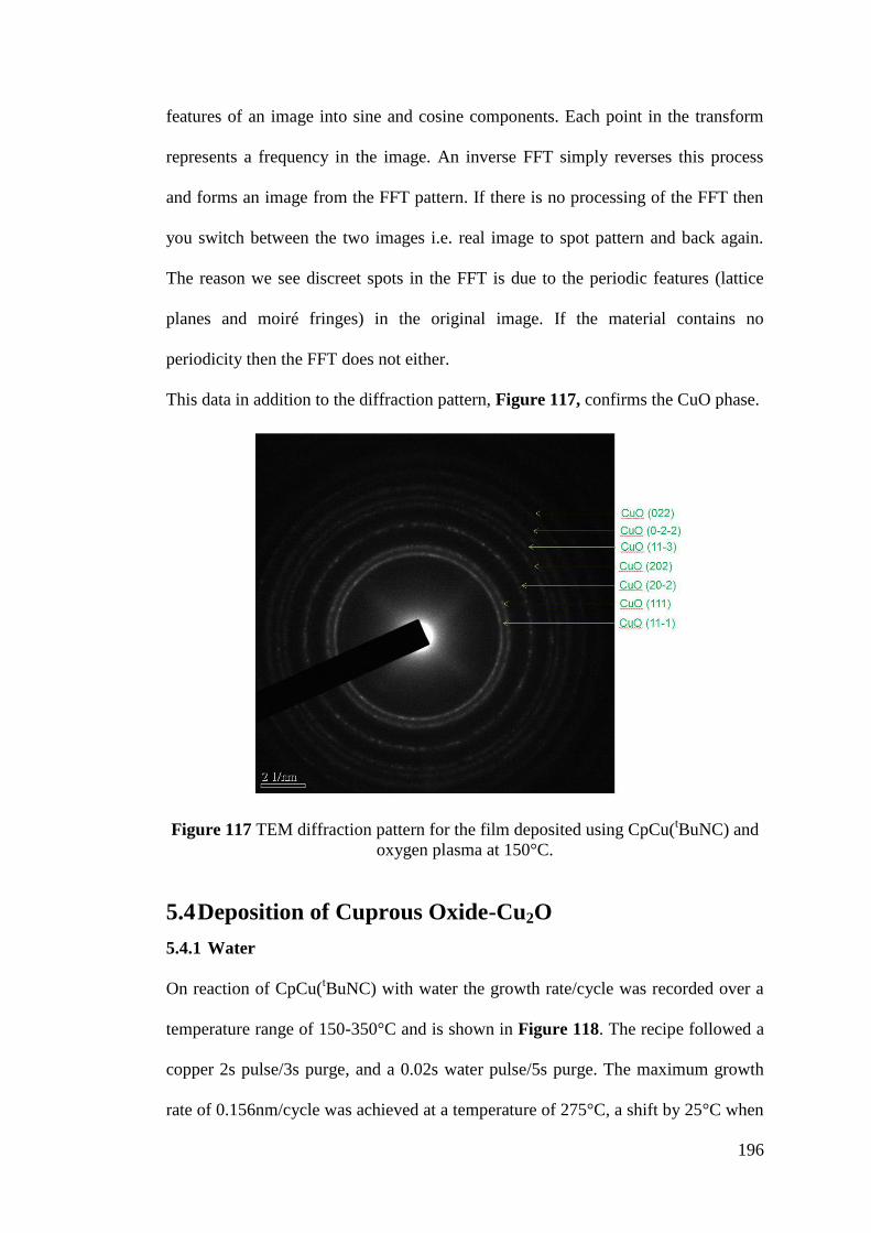
196
features of an image into sine and cosine components. Each point in the transform
represents a frequency in the image. An inverse FFT simply reverses this process
and forms an image from the FFT pattern. If there is no processing of the FFT then
you switch between the two images i.e. real image to spot pattern and back again.
The reason we see discreet spots in the FFT is due to the periodic features (lattice
planes and moiré fringes) in the original image. If the material contains no
periodicity then the FFT does not either.
This data in addition to the diffraction pattern, Figure 117, confirms the CuO phase.
Figure 117 TEM diffraction pattern for the film deposited using CpCu(tBuNC) and
oxygen plasma at 150°C.
5.4 Deposition of Cuprous Oxide-Cu2O
5.4.1 Water
On reaction of CpCu(tBuNC) with water the growth rate/cycle was recorded over a
temperature range of 150-350°C and is shown in Figure 118. The recipe followed a
copper 2s pulse/3s purge, and a 0.02s water pulse/5s purge. The maximum growth
rate of 0.156nm/cycle was achieved at a temperature of 275°C, a shift by 25°C when
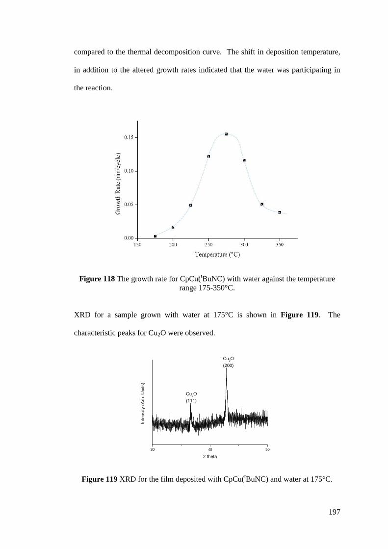
197
compared to the thermal decomposition curve. The shift in deposition temperature,
in addition to the altered growth rates indicated that the water was participating in
the reaction.
Figure 118 The growth rate for CpCu(tBuNC) with water against the temperature
range 175-350°C.
XRD for a sample grown with water at 175°C is shown in Figure 119. The
characteristic peaks for Cu2O were observed.
30 40 50
Cu2O
(200)
Inte
nsity (
Arb
. U
nits)
2 theta
Cu2O
(111)
Figure 119 XRD for the film deposited with CpCu(tBuNC) and water at 175°C.
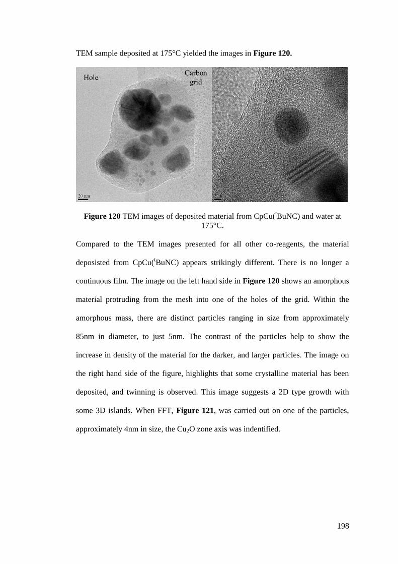
198
TEM sample deposited at 175°C yielded the images in Figure 120.
Figure 120 TEM images of deposited material from CpCu(tBuNC) and water at
175°C.
Compared to the TEM images presented for all other co-reagents, the material
deposisted from CpCu(tBuNC) appears strikingly different. There is no longer a
continuous film. The image on the left hand side in Figure 120 shows an amorphous
material protruding from the mesh into one of the holes of the grid. Within the
amorphous mass, there are distinct particles ranging in size from approximately
85nm in diameter, to just 5nm. The contrast of the particles help to show the
increase in density of the material for the darker, and larger particles. The image on
the right hand side of the figure, highlights that some crystalline material has been
deposited, and twinning is observed. This image suggests a 2D type growth with
some 3D islands. When FFT, Figure 121, was carried out on one of the particles,
approximately 4nm in size, the Cu2O zone axis was indentified.
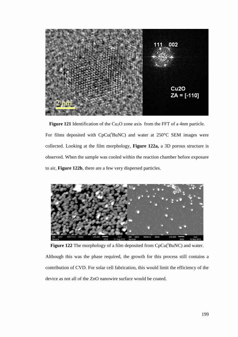
199
Figure 121 Identification of the Cu2O zone axis from the FFT of a 4nm particle.
For films deposited with CpCu(tBuNC) and water at 250°C SEM images were
collected. Looking at the film morphology, Figure 122a, a 3D porous structure is
observed. When the sample was cooled within the reaction chamber before exposure
to air, Figure 122b, there are a few very dispersed particles.
Figure 122 The morphology of a film deposited from CpCu(tBuNC) and water.
Although this was the phase required, the growth for this process still contains a
contribution of CVD. For solar cell fabrication, this would limit the efficiency of the
device as not all of the ZnO nanowire surface would be coated.
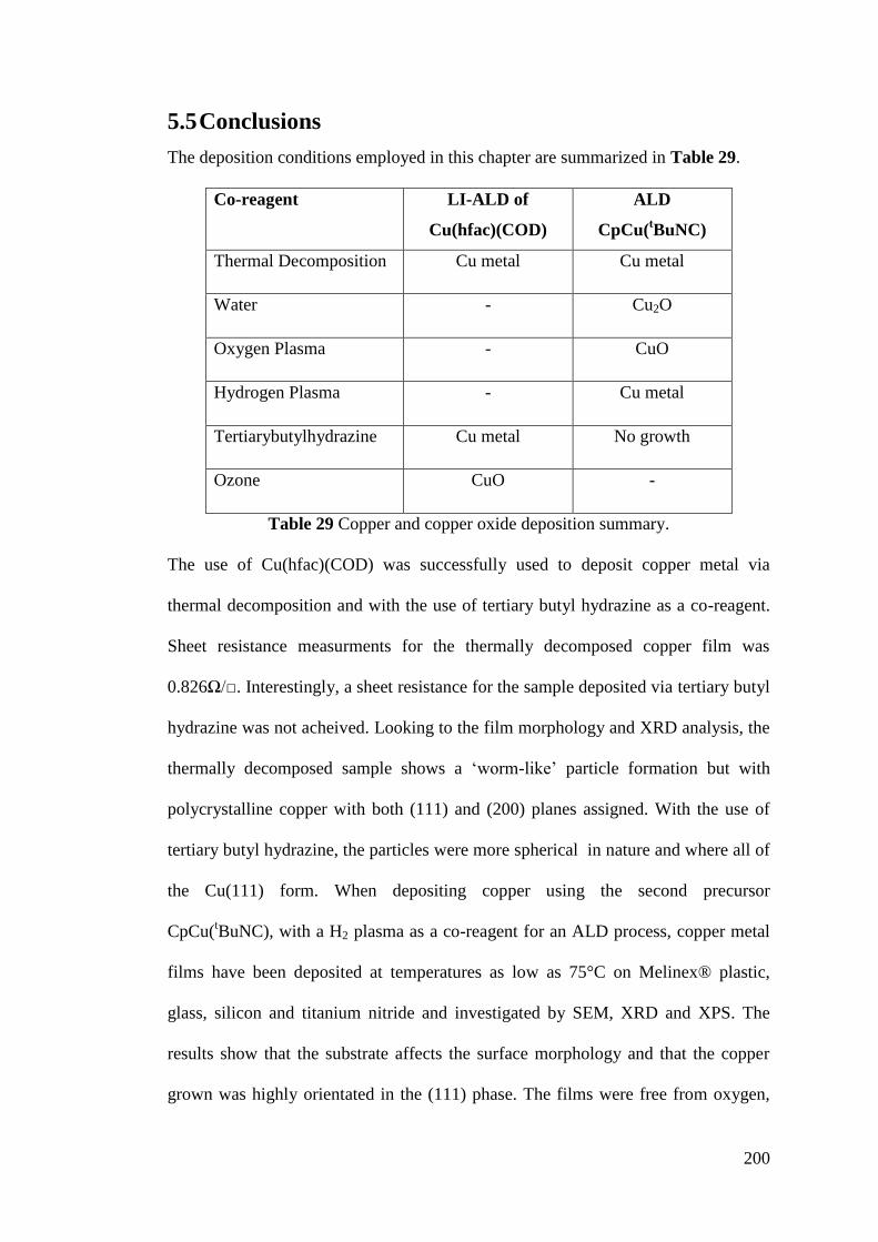
200
5.5 Conclusions
The deposition conditions employed in this chapter are summarized in Table 29.
Co-reagent LI-ALD of
Cu(hfac)(COD)
ALD
CpCu(tBuNC)
Thermal Decomposition Cu metal Cu metal
Water - Cu2O
Oxygen Plasma - CuO
Hydrogen Plasma - Cu metal
Tertiarybutylhydrazine Cu metal No growth
Ozone CuO -
Table 29 Copper and copper oxide deposition summary.
The use of Cu(hfac)(COD) was successfully used to deposit copper metal via
thermal decomposition and with the use of tertiary butyl hydrazine as a co-reagent.
Sheet resistance measurments for the thermally decomposed copper film was
0.826Ω/. Interestingly, a sheet resistance for the sample deposited via tertiary butyl
hydrazine was not acheived. Looking to the film morphology and XRD analysis, the
thermally decomposed sample shows a ‘worm-like’ particle formation but with
polycrystalline copper with both (111) and (200) planes assigned. With the use of
tertiary butyl hydrazine, the particles were more spherical in nature and where all of
the Cu(111) form. When depositing copper using the second precursor
CpCu(tBuNC), with a H2 plasma as a co-reagent for an ALD process, copper metal
films have been deposited at temperatures as low as 75°C on Melinex® plastic,
glass, silicon and titanium nitride and investigated by SEM, XRD and XPS. The
results show that the substrate affects the surface morphology and that the copper
grown was highly orientated in the (111) phase. The films were free from oxygen,
201
carbon and nitrogen contaminants. Sheet resistance measurements on glass show an
average of 0.55Ω/.
Using ozone with Cu(hfac)(COD) resulted in CuO (113) formation at all
temperatures. To deposit CuO with the CpCu(tBuNC) precursor via ALD, an oxygen
plasma was needed, and TEM was used to gain a diffraction pattern to confirm CuO.
For PV applications, Cu2O would be the favoured choice for the p-type material.
This was successfully deposited using CpCu(tBuNC) with water. The film was a
porous structure with some crystalline areas of Cu2O observed.
5.6 Experimental
5.6.1 Precursor synthesis and characterisation
Cu(hfac)(COD) shown in Figure 82 was used as supplied by Sigma-Aldrich and
dissolved in anhydrous toluene. The concentration of the solution was confirmed to
be 0.65M via 1H NMR. The CpCu(
tBuNC) precursor was synthesised using the the
methods of Cotton. 306, 307
All reagents were bought commercially and used without
further purification. The solvents used where anhydrous solvents which were
subsequently passed through a solvent purification system. Standard Schlenck line
techniques were employed with reactions carried out under a positive nitrogen flow.
Freshly cracked cyclopentadiene (18.6g, 0.282 moles) was added to sodium hydride
(11.3g, 0.282 moles) solvated in THF (100 ml). Seperately, a mixture of tBuNC
(23.4g, 0.282moles) in anhydrous THF (100ml) was added to CuCl (27.9g,
0.282moles) in THF (100ml). The NaCp salt was added dropwise to the
ClCutBuNC. The THF was then removed and the product extracted in anhydrous
toluene. As the volume of toluene was reduced, brown/yellow crystals began to
precipitate. A further wash of the crystals with anhydrous hexane and drying under
vacuo yielded a beige solid. Yield: 30g (50%)
202
5.6.2 Growth details
Liquid injection of 0.65M Cu(hfac)(COD) toluene solution held at room temperature
was employed for pulsed CVD and ALD methods. For thermal decomposition
studies, the precursor was injected for 2s, followed by a 2s purge. The overall
reactor pressure was 5 mbar and 200sccm of argon was pushed through the
precursor to aid transportation. The vapouriser and all pipes were maintained at
130°C. For the ALD mode, a 2s precursor pulse and purge was used, followed by
either a 0.5s and 0.1s coreagent pulse in the case of ozone and tertiarybutyl
hydrazine respectively. A 2s co-reagent purge was used in both cases. Due to size
limitations of the stage in the Aixtron reactor, Si(100) and glass were the only
substrates used.
Cyclopentadienyl copper tertiarybutyl isocyanide was held at 100°C for the growth
study. A bubbling system was used with argon (flow rate of 300sccm) as the carrier
gas. Depositions were carried out on an Oxford Instruments OpAL reactor complete
with plasma unit. A pulsed CVD method was used for thermal depositions of copper
metal from CpCu(tBuNC) with no co-reagent. This followed a cyclic 2s precursor
pulse length followed by a 3s purge. With CpCu(tBuNC) and water the pulse purge
train followed 2s Cu pulse/3s Cu purge/0.02s Water pulse/5s Water purge. An ALD
method was employed when O2 or H2 plasma was used as the co-reagent with a 2s
precursor pulse and a 3s precursor purge, followed by a 3s 300W O2 or H2 plasma
exposure and then a 5s purge. Silicon (100) n-doped (2nm SiO2 oxide layer) and
glass substrates were used for the thermal, water and O2 plasma depositions. For the
low temperature plasma growth titanium nitride (TiN) and plastic substrates were
used in addition to silicon and glass. Silicon, titanium nitride and Melinex® plastic

203
were used as purchased with no pre-treatment. Glass used was first cleansed from
oil using isopropanol and then dried using acetone/N2.
204
Chapter 6 Conclusions and Recommendations for Future
Work
This thesis has demonstrated precursor development and investigated chemical
vapour techniques for the deposition of n-type zinc oxide nanowires and p-type
copper oxide thin films. The investigation of all oxide p-n junctions is of interest in
the use of photovoltaic, with absorbing ZnO NWs offering an increased surface area
for light harvesting, helping overall cell efficiency. Dialkylzinc precursors with
oxygen co-reactant can be used to deposit ZnO, although pre-reaction can limit the
control of the film grown. This research revisited the dialkylzinc precursors DEZn
and DMZn and resulted in the successful determination of the solid-state crystal
structures. All three structures contain linear diorganozinc molecules, which interact
through weak intermolecular interactions with small covalent contributions.
Interestingly, Me2Zn undergoes a reversible solid–solid phase transition at 180 K; its
high-temperature phase shows a two-dimensional disorder. DMZn was subsequently
utilised in a series of adduct compounds, [DMZn.L], (where L=1,2-
dimethoxyethane, 1,4-dioxane, or 1,4-thioxane) . Single crystal XRD data for
[DMZn.L] helps to show that [Me2Zn] forms weak adducts with ether ligands. The
1,4-dioxane complex is polymeric with repeating [Me2Zn] units bridged by 1,4-
dioxane ligands. By contrast the 1,2-dimethoxyethane complex has a monomeric
structure containing both bidentate and chelating ligands. The 1,4-thioxane
precursor forms even weaker interactions with [Me2Zn] and the solid-state structure
can be regarded as an intermediate between a coordination complex and a co-crystal.
By using the adducted compounds for ZnO deposition, the pre-reaction is avoided.
LI-MOCVD was the technique employed and with careful selection of substrate
temperature and the II:VI ratio of zinc to oxygen, the structure of the nanowires
205
could be controlled. Thin film analysis was carried out to characterise the
morphology and electronic properties of the deposited material. SEM experiments
enabled imaging of the microstructure helping to compare and contrast the density
and size of the NWs and how this varies with the ligand system used, the substrate
and the deposition time. For all the [DMZn.L] compounds with oxygen adducts at
500°C, all of the films showed nanowire formation, a slightly elevated temperature
of 550°C was needed for NW formation from the thioxane adduct. All ZnO samples
deposited were confirmed to be of the wurtizitic phase by XRD. Raman
spectroscopy help to demonstrate NW diameters of between 40-100nm. The
photoluminescence data in conjunction with the AES composition data helped to
confirm the incorporation of sulphur into the final films, adding weight to the claim
that the ligand system plays a part in the CVD reaction.
Copper oxide deposition was investigated both by LI-ALD using Cu(hfac)(COD)
and by plasma-assisted ALD using CpCu(tBuNC). In this thesis it is demonstrated
that a pulsed Li-ALD approach can be exploited to deposit CuO with ozone as the
co-reagent. Copper metal with a sheet resistance of 0.826Ω/ was achieved
following thermal decomposition.Although CpCu(tBuNC) has previously been
reported for CVD, this research is the first successful attempt to employ it as an
ALD precursor. This work demonstrates that by tailoring the co-reagents, Cu, CuO
and Cu2O can be deposited with hydrogen plasma, oxygen plasma and water
respectively. SEM and TEM techniques have proven invaluable in understanding
film morphology, and to also gain crystal diffraction data for very thin films,
enabling sucessful characterisation of the film grown. The metallic copper
deposition was successful at temperatures as low as 75°C with a sheet resistance of
0.55Ω/. It has been demonstrated that copper can be deposited on many substrates

206
(e.g. glass, Si, TiN and Melinex® plastic without the need for a seed layer. XPS and
EDX have helped to confirm the high purity.
Recommendations for future work would include the process optimisation for the
copper and copper oxide deposition.Work is currently underway to investigate the
manufacture of thin film solar cells using CpCu(tBuNC) to deposit Cu2O on CdSe
absorber layers. The wider scope would be to construct the target PV cell after fully
characterising all consituents. A measurement on solar cell efficieny could help to
determine if solar cell manufacture of this type would be suitable for industry.
207
Chapter 7 References
1 . Nelson, J.; The Physics of Solar Cells; Imperial College Press, 2003.
2 . http://www.britannica.com/EBchecked/topic/183144/electrolyte Encyclopedia
Britanica Online, 2013.
3 . Zweibel, K.;Hersch, P.; Basic Photovoltaic Principles and Methods, Solar
Energy Research Institute; Van Nostrand Reinhold, 1984.
4 . http://pveducation.org/pvcdrom/manufacturing/czochralski-silicon PV Education
Organisation, 2013.
5 . http://www.ise.fraunhofer.de/en/press-and-media/press-
releases/presseinformationen-2013/world-record-solar-cell-with-44.7-efficiency
Fraunhofer ISE, October 2013.
6 . Green, M. A.;Emery, K.;Hishikawa, Y.; Prog Photovoltaics Res Appl, 2013, 21
(1) p1-11.
7 . Olmsted,J.;Williams,G. M.; Band Theory of Solids in Chemistry:The Molecular
Science, 2nd Edition; Wm. C. Brown, 1997.
8 . Whittaker,A. G.;Mount,A. R.; Semiconductors-bands in Instant Notes:Physical
Chemistry; BIOS Scientific Publishers, 2000.
9 . Kittel, C.; Introduction to Solid State Physics; John Wiley, 2005.
10 . https://energypedia.info/wiki/Solar_Cells_and_Modules Energypedia, 2013.
208
11 . http://www.dur.ac.uk/renewable.energy/solarpower/pv-how_it_works/ Durham
University, 2012.
12 . Parker, G.; Introductory Semiconductor Device Physics; Institute of Physics,
2004.
13 . Colinge, J. P.;Colinge, C. A.; Physics of Semiconductor Devices; Springer,
2002.
14 . www1.gantep.edu.tr/~bgonul/dersnotlari/sc/CHAPTER_2.ppt Gaziantep
Universitesi, 2012.
15 . http://www.students.tut.fi/~khamousk/semi.html Tampere University of
Technology, 2012.
16 . Shockley, W.; Bell System Technical Journal, 1949, 28 (3) p435-489.
17 . Shockley, W.; Electrons and Holes in Semiconductors. Van Nostrand, 1950.
18 . Sah, C. T.;Noyce, R. N.;Shockley, W.; Proceedings of the IRE, 1957, 45 (9)
p1228-1243.
19 . Moll, J. L.; Proceedings of the IRE, 1958, 46 (6) p1076-1082.
20 . http://www.electronics-tutorials.ws/diode/diode_3.html Electronic Tutorials,
2012.
21 . Green, M. A.; Solar Cells:Operating Principles, Technology and System
Applications; Prentice-Hall, 1982.
209
22 . http://chemistry.beloit.edu/edetc/SlideShow/slides/contents/pn.html University
of Wisconsin, 2012.
23 . Ginley, D. S.;Cahen, D.; Fundamental of Materials for Energy and
Environmental Sustainability. Materials Research Society, Cambridge University
Press, 2012.
24 . Van de Walle, C. G.;Neugebauer, J.; Nature, 2003, 423 (6940) p626-628.
25 . Ichimura, M.;Song, Y.; Jpn. J. Appl. Phys., 2011, 50 p051002.
26 . Jeong, S.;Aydil, E. S.; J. Cryst. Growth, 2009, 311 (17) p4188-4192.
27 . Shao,G.;Luo,J. University of Bolton. Photovoltaic cell based on transition
metal oxides of varied band gaps and p/n types.30/06/2012GB2466496.
28 . Lv, P.;Zheng, W.;Lin, L.; Physica B: Condensed Matter, 2011, 406 (6–7)
p1253-1257.
29 . Chiang, C.;Aroh, K.;Franson, N.; Int J Hydrogen Energy, 2011, 36 (24)
p15519-15526.
30 . Caballero-Briones, F. Art s, . M. D ez-P rez, I. J. Phys. Chem. C, 2009, 113
(3) p1028-1036.
31 . Kramm, B.;Laufer, A.;Reppin, D.; Appl. Phys. Lett., 2012, 100 (9) p094102.
32 . Robertson, J.;Clark, S. J.; Phys. Rev. B, 2011, 83 (7) p075205-075212.
33 . Wong, L. M.;Chiam, S. Y.;Wang, S. J.; J. Appl. Phys., 2010, 108 (3) p033702-
033708.
210
34 . Hsueh, T.;Hsu, C.;Chang, S.; Scr. Mater., 2007, 57 (1) p53-56.
35 . Bu, I. Y. Y.; Ceram. Int., 2013, 39 (7) p8073-8078.
36 . Wang, P.;Zhao, X.;Li, B.; Opt. Express, 2011, 19 (12) p11271-11279.
37 . Jeong, S. S.;Mittiga, A.;Salza, E.; Electrochim. Acta, 2008, 53 (5) p2226-2231.
38 . Mittiga, A.;Salza, E.;Sarto, F.; Appl. Phys. Lett., 2006, 88 (16) p163502-
163503.
39 . Hussain, S.;Cao, C.;Nabi, G.; Electrochim. Acta, 2011, 56 (24) p8342-8346.
40 . Chen, J.;Perng, D.;Fang, J.; Solar Energy Mater. Solar Cells, 2011, 95 (8)
p2471-2477.
41 . Wang, Y.;She, G.;Xu, H.; Mater Lett, 2012, 67 (1) p110-112.
42 . Wei, H.;Gong, H.;Wang, Y.; CrystEngComm, 2011, 13 (20) p6065-6070.
43 . Kidowaki, H.;Oku, T.;Akiyama, T.; IJRRAS, 2012, 13 (1) p67-72.
44 . Pilkington,A.;Proceedings of the Royal Society of London Series A-
Mathematical and Physical Sciences , 16th December 1969, London, 314, (1516), 1-
25.
45 . http://asmcommunity.asminternational.org/portal/site/www/SubjectGuideItem/;
ASM International, 2013.
46 . http://www.beneq.com/transparent-conductive-oxide-tco.html Beneq, 2013.
211
47 . Pakin,I. P.;Palgrave,R. G.; CVD of functional Coatings on Glass in Chemical
Vapour Deposition, Precursors, Processes and Applications; Royal Society of
Chemistry, 2009.
48 . Ban, T.;Ohya, Y.;Takahashi, Y.; J. Appl. Phys., 1998, 83 (5) p2631-2645.
49 . Edwards, P. P.;Porch, A.;Jones, M. O.; Dalton Trans., 2004, (19) p2995-3002.
50 . Hamberg, I.;Granqvist, C. G.; J. Appl. Phys., 1986, 60 (11) pR123-R160.
51 . Kamei, M.;Enomoto, H.;Yasui, I.; Thin Solid Films, 2001, 392 (2) p265-268.
52 . Paine, D. C.;Whitson, T.;Janiac, D.; J. Appl. Phys., 1999, 85 (12) p8445-8450.
53 . Chen, C. H.;Chang, S. J.;Su, Y. -.; Photonics Technology Letters, IEEE, 2001,
13 (8) p848-850.
54 . Sheu, J. K.;Su, Y. K.;Chi, G. C.; Appl. Phys. Lett., 1998, 72 (25) p3317-3319.
55 . Kim, S. T.;Lee, J. H.;Yang, J. Y.; J. Korean Phys. Soc., 2007, 50 (3) p662-665.
56 . Sittinger,V.;Ruske,F.;Werner,W.;5th International Symposium on Transparent
Oxide Thin Films for Electronics and Optics, 7/1, 516, (17), 5847-5859.
57 . Horng, R.;Wuu, D.;Lien, Y.; Appl. Phys. Lett., 2001, 79 (18) p2925-2927.
58 . Law, M.;Greene, L. E.;Johnson, J. C.; Nat Mater, 2005, 4 (6) p455-459.
59 . Wu, J.;Chen, G.;Yang, H.; Appl. Phys. Lett., 2007, 90 (21) p213109.
60 . Baxter, J. B.;Aydil, E. S.; Appl. Phys. Lett., 2005, 86 (5) p053114.
212
61 . Colavita, P. E.;Sun, B.;Wang, X.; J. Phys. Chem. C, 2009, 113 (4) p1526-1535.
62 . You, J. B.;Zhang, X. W.;Cai, P. F.; Appl. Phys. Lett., 2009, 94 (26) p262105.
63 . Gordon, R. G.; MRS Bull, 2000, 25 (08) p52.
64 . Yang, F.;Forrest, S. R.; Adv Mater, 2006, 18 (15) p2018-2022.
65 . Mondragón-Suárez, H.;Maldonado, A.;Olvera, M. d. l. L.; Appl. Surf. Sci.,
2002, 193 (1–4) p52-59.
66 . Seeber, W. T.;Abou-Helal, M. O.;Barth, S.; Materials Science in Semiconductor
Processing, 1999, 2 (1) p45-55.
67 . Jiménez-González, A. E.;Soto Urueta, J. A.;Suárez-Parra, R.; J. Cryst. Growth,
1998, 192 (3–4) p430-438.
68 . Schuler, T.;Aegerter, M. A.; Thin Solid Films, 1999, 351 (1–2) p125-131.
69 . Musat, V.;Teixeira, B.;Fortunato, E.; Surface and Coatings Technology, 2004,
180–181 (0) p659-662.
70 . Lin, S. Huang, . Šajgalik, P. Surface and Coatings Technology, 2005, 190 (1)
p39-47.
71 . Oh, B.;Jeong, M.;Lee, W.; J. Cryst. Growth, 2005, 274 (3–4) p453-457.
72 . Zhang, D. H.;Yang, T. L.;Wang, Q. P.; Mater. Chem. Phys., 2001, 68 (1–3)
p233-238.
213
73 . Fenske, F.;Fuhs, W.;Nebauer, E.; Thin Solid Films, 1999, 343–344 (0) p130-
133.
74 . Elam, J. W.;George, S. M.; Chem. Mater., 2003, 15 (4) p1020-1028.
75 . Kim, Y.;Kim, H.; Mater Lett, 1999, 41 (4) p159-163.
76 . Groenen, R.;Löffler, J.;Sommeling, P. M.; Thin Solid Films, 2001, 392 (2)
p226-230.
77 . Lee, S.;Han, S.;Jung, H. S.; J. Phys. Chem. C, 2010, 114 (15) p7185-7189.
78 . Saito, K.;Hiratsuka, Y.;Omata, A.; Superlattices and Microstructures, 2007, 42
(1–6) p172-175.
79 . Chalker, P. R.;Marshall, P. A.;Romani, S.; MRS Online Proceedings Library,
2011, 1315 .
80 . Chalker, P. R.;Marshall, P. A.;Roberts, J. W.; J. Vac. Sci. Technol. A, 2013,
31 (1) p01A120.
81 . Irvine, S. J. C.;Barrioz, V.;Lamb, D.; J. Cryst. Growth, 2008, 310 (23) p5198-
5203.
82 . Krupanidhi, S. B.;Maffei, N.;Sayer, M.; J. Appl. Phys., 1983, 54 (11) p6601-
6609.
83 . Sreenivas, K.;Sayer, M.;Baar, D. J.; Appl. Phys. Lett., 1988, 52 (9) p709-711.
84 . Ramesh, R.;Inam, A.;Chan, W. K.; Appl. Phys. Lett., 1991, 59 (27) p3542-
3544.
214
85 . Manasevit, H. M.; J. Cryst. Growth, 1981, 55 (1) p1-9.
86 . Shuster, G.;Kreinin, O.;Lakin, E.; Thin Solid Films, 2010, 518 (16) p4658-4661.
87 . Jones, A. C.;Leedham, T. J.;Wright, P. J.; Chemical Vapor Deposition, 1998, 4
(2) p46-49.
88 . Legrand, J.;Lhostis, S.;Chang, Y.; Microelectronic Engineering, 2004, 72 (1–4)
p310-314.
89 . Suntola, T.; Materials Science Reports, 1989, 4 (5) p261-312.
90 . http://www.picosun.com Picosun, 2013.
91 . Ritala, M.;Niinisto, J.; Chemical Vapour Deposition; The Royal Society of
Chemistry, 2009.
92 . Jones, A. C.;Aspinall, H. C.;Chalker, P. R.; Chemical Vapor Deposition, 2006,
12 (2-3) p83-98.
93 . http://www.zinc.org/ Zinc.Org, 2012.
94 . http://minerals.usgs.gov/minerals/pubs/commodity/zinc/mcs-2011-zinc.pdf US
Gov, 2012.
95 . Knochel, P.;Singer, R. D.; Chem. Rev., 1993, 93 (6) p2117-2188.
96 . Frankland, E. Q.; J. Chem. Soc, 1850, 2 p263.
97 . Frankland, E. Q.; Liebigs Ann. Chem., 1949, 71 p171.
215
98 . Haaland, A.;Green, J. C.;McGrady, G. S.; Dalton Trans., 2003, (22) p4356-
4366.
99 . Seyferth, D.; Organometallics, 2001, 20 (14) p2940-2955.
100 . Antes, I.;Frenking, G.; Organometallics, 1995, 14 (9) p4263-4268.
101 . Almenningen, A.; Acta Chem. Scand., 1982, A36 p159.
102 . Bacsa, J.;Hanke, F.;Hindley, S.; Angewandte Chemie International Edition,
2011, 50 (49) p11685-11687.
103 . O'Brien,P.; Cadmium and Zinc in Comprehensive Organometallic Chemistry
II: A Review od the Literature 1982-1994; Elsevier Science Ltd., 1995.
104 . Van Der Kerk, G. J. M.; Pure Appl. Chem., 1972, 30 (3-4) p389-408.
105 . Thiele, K.; Zeitschrift Für Anorganische Und Allgemeine Chemie, 1963, 322
(1-2) p71-80.
106 . Hindley, S.;Jones, A. C.;Ashraf, S.; Journal of Nanoscience and
Nanotechnology, 2011, 11 (9) p8294.
107 . O'Brien, P.;Walsh, J. R.;Jones, A. C.; J. Mater. Chem., 1993, 3 (7) p739-742.
108 . O'Brien, P.;Malik, M. A.;Walsh, J. R.; Advanced Materials for Optics and
Electronics, 1997, 7 (3) p117-121.
109 . Thiele, K.; Zeitschrift Für Anorganische Und Allgemeine Chemie, 1963, 325
(3-4) p156-168.
216
110 . Coates, G. E.;Ridley, D.; J. Chem. Soc., 1965, 0 (0) p1870-1877.
111 . Butlerow, M. A.; Jahresber., 1864, 467 .
112 . Shearer, H. M. M.;Spencer, C. B.; Chem. Commun. (London), 1966, 0 (7)
p194a-194a.
113 . Jana, S.;Berger, R. J. F.;Fröhlich, R.; Inorg. Chem., 2007, 46 (10) p4293-4297.
114 . Bunn, C. W.; Proceedings of the Physical Society, 1935, 47 (5) p835.
115 . Jagadish,C.;Coleman,V. A.; Basic properties and applications of ZnO in Zinc
oxide bulk, thin films and nanostructures : processing, properties and applications;
Elsevier, 2006.
116 . Ashrafi, A. B. M. A.;Ueta, A.;Avramescu, A.; Appl. Phys. Lett., 2000, 76 (5)
p550-552.
117 . Kim, S.;Jeong, S.;Cho, C.; Appl. Phys. Lett., 2003, 82 (4) p562-564.
118 . Bates, C. H.;White, W. B.; Science, 1962, 137 (3534) p993-993.
119 . http://www.wiley-vch.de/books/sample/3527408134_c01.pdf) Wiley, 2012.
120 . Look,D. C.; Doping and defects in ZnO in Zinc oxide bulk, thin films and
nanostructures : processing, properties and applications; Elsevier, 2006.
121 . Phillips, J. C.; Bonds and Bands in Semiconductors; Academic Press, 1973.
122 . Lide, D. R.; CRC Handbook of Chemistry and Physics: 73rd Edition; CRC
Press, 1992.
217
123 . Özgür, Ü;Alivov, Y.;Liu, C.; J. Appl. Phys., 2005, 98 (4) p041301.
124 . Himpsel, F. J.; Advances in Physics, 1983, 32 p1-51.
125 . Rössler, U.; Phys. Rev., 1969, 184 (3) p733-738.
126 . Franklin, L.;Ekuma, C. E.;Zhao, G. L.; Journal of Physics and Chemistry of
Solids, 2013, 74 (5) p729-736.
127 . Vogel, D.;Kruger, P.;Johannes, P.; Phys. Rev. B, 1995, 52 (20) pR14316-
R14319.
128 . Wei, S. H.;Zunger, A.; Phys. Rev. B, 1988, 37 (15) p8958-8981.
129 . Schröer, P.;Krüger, P.;Pollmann, J.; Phys. Rev. B, 1993, 47 (12) p6971-6980.
130 . Xu, Y.;Ching, W. Y.; Phys. Rev. B, 1993, 48 (7) p4335-4351.
131 . Schröer, P.;Krüger, P.;Pollmann, J.; Phys. Rev. B, 1994, 49 (24) p17092-
17101.
132 . Perdew, J. P.; Phys. Rev. B, 1981, 23 (10) p5048-5079.
133 . Iwata, K.;Fons, P.;Niki, S.; Physica Status Solidi (a), 2000, 180 (1) p287-292.
134 . Kazuhiro, M.;Michihiro, S.;Hiroyuki, K.; Jpn. J. Appl. Phys., 2002, 41 (Part
2, No. 11A) pL1203-L1205.
135 . Miyamoto, K.;Sano, M.;Kato, H.; J. Cryst. Growth, 2004, 265 (1–2) p34-40.
136 . Kaidashev, E. M.;Lorenz, M.;von Wenckstern, H.; Appl. Phys. Lett., 2003, 82
(22) p3901-3903.
218
137 . Albrecht, J. D.;Ruden, P. P.;Limpijumnong, S.; J. Appl. Phys., 1999, 86 (12)
p6864-6867.
138 . Look, D. C.;Hemsky, J. W.;Sizelove, J. R.; Phys. Rev. Lett., 1999, 82 (12)
p2552-2555.
139 . Look, D. C.;Reynolds, D. C.;Sizelove, J. R.; Solid State Commun., 1998, 105
(6) p399-401.
140 . Adachi,S.; Thermal Properties in Properties of Semiconductor Alloys; John
Wiley & Sons, Ltd, 2009.
141 . Ibach, H.; Physica Status Solidi (B), 1969, 33 (1) p257-265.
142 . Klingshirn,C.; Intrinsic Linear Optical Properties Close to the Fundamental
Absorption Edge in Springer Berlin Heidelberg, 2010.
143 . Florescu, D. I.;Mourokh, L. G.;Pollak, F. H.; J. Appl. Phys., 2002, 92 (2)
p890-892.
144 . Chennupati, E. J.;Pearton, S. J.; Zinc Oxide Bulk, Thin Films and
Nanostructures : Processing, Properties and Applications; Elsevier, 2006.
145 . Smith, F. T. J.; Appl. Phys. Lett., 1983, 43 (12) p1108-1110.
146 . Roth, A. P.;Williams, D. F.; J. Appl. Phys., 1981, 52 (11) p6685-6692.
147 . Kern, W.;Heim, R.; J. Electrochem. Soc., 1970, 117 (4) p562-568.
148 . Ghandhi, S. K.;Field, R. J.;Shealy, J. R.; Appl. Phys. Lett., 1980, 37 (5) p449-
451.
219
149 . Park, W. I.;An, S.;Yi, G.; J. Mater. Res., 2001, 16 (05) p1358-1362.
150 . Park, W. I.;Yi, G.;Jang, H. M.; Appl. Phys. Lett., 2001, 79 (13) p2022-2024.
151 . Gorla, C. R.;Emanetoglu, N. W.;Liang, S.; J. Appl. Phys., 1999, 85 (5)
p2595-2602.
152 . Zhang, B.;Manh, L.;Wakatsuki, K.; Jpn. J. Appl. Phys., 2003, 42 p2291-
2295.
153 . Ma, Y.;Du, G. T.;Yang, T. P.; J. Cryst. Growth, 2003, 255 (3–4) p303-307.
154 . Ma, Y.;Du, G. T.;Yang, S. R.; J. Appl. Phys., 2004, 95 (11) p6268-6272.
155 . Lau, C. K.;Tiku, S. K.;Lakin, K. M.; J. Electrochem. Soc., 1980, 127 (8)
p1843-1847.
156 . Yasuda, T.;Segawa, Y.; Physica Status Solidi (B), 2004, 241 (3) p676-679.
157 . Solanki, R.;Collins, G. J.; Appl. Phys. Lett., 1983, 42 (8) p662-663.
158 . Ogata, K.;Kawanishi, T.;Maejima, K.; J. Cryst. Growth, 2002, 237–239, Part 1
(0) p553-557.
159 . Ogata, K.;Maejima, K.;Fujita, S.; J. Cryst. Growth, 2003, 248 (0) p25-30.
160 . Dadgar, A.;Oleynik, N.;Forster, D.; J. Cryst. Growth, 2004, 267 (1–2) p140-
144.
161 . Gruber, T.;Kirchner, C.;Thonke, K.; Physica Status Solidi (a), 2002, 192 (1)
p166-170.
220
162 . Oleynik, N.;Adam, M.;Krtschil, A.; J. Cryst. Growth, 2003, 248 (0) p14-19.
163 . Oda, S.;Tokunaga, H.;Kitajima, N.; Jpn. J. Appl. Phys, 1985, 24 p1607-
1610.
164 . Kirchner, C.;Gruber, T.;Reuß, F.; J. Cryst. Growth, 2003, 248 (0) p20-24.
165 . Auld, J.;Houlton, D. J.;Jones, A. C.; J. Mater. Chem., 1994, 4 (8) p1249.
166 . Lad, R. J.;Funkenbusch, P. D.;Aita, C. R.; J. Vac. Sci. Technol., 1980, 17 (4)
p808-811.
167 . Yamamoto, T.;Shiosaki, T.;Kawabata, A.; J. Appl. Phys., 1980, 51 (6) p3113-
3120.
168 . Hwang, D.;Bang, K.;Jeong, M.; J. Cryst. Growth, 2003, 254 (3–4) p449-455.
169 . Hachigo, A.;Nakahata, H.;Higaki, K.; Appl. Phys. Lett., 1994, 65 (20) p2556-
2558.
170 . Mitsuyu, T.;Ono, S.;Wasa, K.; J. Appl. Phys., 1980, 51 (5) p2464-2470.
171 . Wright, P. J.;Cockayne, B.;Williams, A. J.; J. Cryst. Growth, 1987, 84 (3)
p552-554.
172 . Wright, P. J.;Cockayne, B.;Jones, A. C.; Chemtronics, 1988, 3 p35.
173 . Cockayne, B.;Wright, P. J.;Armstrong, A. J.; J. Cryst. Growth, 1988, 91 (1–2)
p57-62.
221
174 . Wright, P. J.;Parbrook, P. J.;Cockayne, B.; J. Cryst. Growth, 1989, 94 (2)
p441-447.
175 . Wright, P. J.;Cockayne, B.;Parbrook, P. J.; J. Cryst. Growth, 1990, 104 (3)
p601-609.
176 . Yates, H. M.;Williams, J. O.; J. Cryst. Growth, 1991, 107 (1–4) p386-389.
177 . Jensen, K. F.;Annapragada, A.;Ho, K. L.; J. Phys. IV France, 1991, 02 (C2)
p243-252.
178 . Foster, D. F.;Patterson, I. L. J.;James, L. D.; Advanced Materials for Optics
and Electronics, 1994, 3 (1-6) p163.
179 . Huh, J.;Patnaik, S.;Jensen, K.; J Electron Mater, 1993, 22 (5) p509.
180 . Wright, P. J.;Cockayne, B.;Jones, A. C.; J. Cryst. Growth, 1988, 91 (1–2) p63-
66.
181 . Jones, A. C.;Rushworth, S. A.;O'Brien, P.; J. Cryst. Growth, 1993, 130 (1–2)
p295-299.
182 . Cloitre, T.;Briot, N.;Briot, O.; Materials Science and Engineering: B, 1993, 21
(2–3) p169-173.
183 . Khan, O. O’Brien, P. Hamilton, P. A. Chemitronics, 1989, 4 (21) p412.
184 . Xu, J.;Pan, Q.;Shun, Y.; Sensors Actuators B: Chem., 2000, 66 (1–3) p277-
279.
185 . Huang, M. H.;Mao, S.;Feick, H.; Science, 2001, 292 (5523) p1897-1899.
222
186 . Bao, J.;Zimmler, M.;Capasso, F.; Nano Lett., 2006, 6 (8) p1719-1722.
187 . Gonzalez-Valls, I.;Lira-Cantu, M.; Energy Environ. Sci., 200, 2 (1) p19-34.
188 . Yu, D.;Trad, T.;McLeskey, J.; Nanoscale Research Letters, 2010, 5 (8) p1333-
1339.
189 . Beek, W. J. E.;Wienk, M. M.;Janssen, R. A. J.; Adv Mater, 2004, 16 (12)
p1009-1013.
190 . Unalan, H. E.;-Hiralal, P.;Kuo, D.; J. Mater. Chem., 2008, 18 (48) p5909-
5912.
191 . Zhang, Y.;Ram, M.;Stefanakos, E.; Journal of Nanomaterials, 2012, 2012 p1-
22.
192 . Park, W. I.;Kim, D. H.;Jung, S. W.; Appl. Phys. Lett., 2002, 80 (22) p4232-
4234.
193 . Liu, X.;Wu, X.;Cao, H.; J. Appl. Phys., 2004, 95 (6) p3141-3147.
194 . Kwak, C. H.;Kim, B. H.;Park, S. H.; J. Cryst. Growth, 2009, 311 (20) p4491-
4494.
195 . Kaufmann, T.;Fuchs, G.;Webert, M.; Crystal Research and Technology, 1989,
24 (3) p269-274.
196 . Black, K.;Chalker, P. R.;Jones, A. C.; Chemical Vapor Deposition, 2010, 16
(1-3) p106-111.
223
197 . http://www.chemistryexplained.com/elements/C-
K/Copper.html#ixzz2BSQ7IPyp Thompson Corporation, 2013.
198 . http://www.uncp.edu/home/mcclurem/ptable/copper/cu.htm University of
North Carolina, Pembroke, 2013.
199 .
http://asmcommunity.asminternational.org/portal/site/www/SubjectGuideItem/?vgne
xtoid=ad7cdc8cc359d210VgnVCM100000621e010aRCRD ASM International, The
Materials Information Society, 2013.
200 . Giancoli, D. C.; Physics for Scientists & Engineers with Modern Physics /
Douglas C. Giancoli; Upper Saddle River, N.J. : Pearson Prentice Hall, 2009; 4th
ed, 2009.
201 . Zant, P. V.; Microchip Fabrication: A Practical Guide to Semiconductor
Processing; McGraw-Hill Education, 2004.
202 . Willcocks,A. M. Development of Coinage Metal Precursor for Chemical
Vapour Depostion (CVD) and Atomic Layer Depositon (ALD); 2011, University of
Bath, Department of Chemistry.
203 .
http://domino.research.ibm.com/comm/wwr_thinkresearch.nsf/pages/copper397.htm
l IBM, 2013.
204 . http://www.advanced-energy.com/upload/file/white_papers/sl-electroplating-
270-01.pdf AnabellePratt, Advanced Energy, 2013.
224
205 . Andricacos, P., C.; The Electrochemical Society Interface, 1999, p32-37.
206 . Campbell, S. A.; The Science and Engineering of Microelectronic
Fabrication; New York: Oxford University Press, 2001.
207 .
http://www.matweb.com/search/DataSheet.aspx?MatGUID=859664f9f59f46bb958e
99a063aec4b5 MatWeb LLC, 2013.
208 . Oku, T.;Motoyoshi, R.;Fujimoto, K.; Journal of Physics and Chemistry of
Solids, 2011, 72 (11) p1206-1211.
209 . Haukka,S.;Lakomaa,E. L.; Adsorption controlled preparation of heterogeneous
catalysts in Studies in Surface Science and Catalysis; Elsevier, .
210 . Wagh, M. S.;Patil, L. A.;Seth, T.; Mater. Chem. Phys., 2004, 84 (2–3) p228-
233.
211 . S Hüfner and M A Hossain and A Damascelli and,G.A.Sawatzky; Reports on
Progress in Physics, 2008, 71 (6) p062501.
212 . Bugarinovi ,S. Rajči -Vujasinovi ,M. Cuprous Oxide as an Active Material
for Solar Cells in Solar Cells-New Aspects and Solutions; InTech, 2011.
213 . Kim, D.;Wentorf, R. H.;Gill, W. N.; Journal of the Electrochemical Society,
1993, 140 (11) p3267-3272.
214 . Lakshmanan, S. K.;Gill, W. N.; J. Vac. Sci. Technol. A, 1998, 16 (4) p2187-
2197.
225
215 . Juppo, M.;Ritala, M.;Leskela, M.; J. Vac. Sci. Technol. A, 1997, 15 (4) p2330-
2333.
216 . Hampden-Smith,M. J.;Kodas,T. T.; Chemical Vapor Deposition of Copper
from Cu(I) Compounds in The Chemistry of Metal CVD; Wiley-VCH Verlag
GmbH, 2007.
217 . Vertoprakhov, V.;Krupoder, S.; Russ. Chem. Rev., 2000, 69 (12) p1057-1082.
218 . Nguyen, T.;Charneski, L. J.;Hsu, S. T.; Journal of the Electrochemical Society,
1997, 144 (8) p2829-2833.
219 . Lin, C.;Chen, P.;Lin, Y.; Journal of the Electrochemical Society, 2003, 150 (7)
pC451-C456.
220 . Jakob, A.;Shen, Y.;Wächtler, T.; Zeitschrift Für Anorganische Und
Allgemeine Chemie, 2008, 634 (12-13) p2226-2234.
221 . Mothes, R.;Ruffer, T.;Shen, Y.; Dalton Trans., 2010, 39 (46) p11235-11247.
222 . Van Hemert, R. L.;Spendlove, L. B.;Sievers, R. E.; Journal of the
Electrochemical Society, 1965, 112 (11) p1123-1126.
223 . Bertrand, J. A.;Kaplan, R. I.; Inorg. Chem., 1966, 5 (3) p489-491.
224 . Maverick, A. W.;Fronczek, F. R.;Maverick, E. F.; Inorg. Chem., 2002, 41 (24)
p6488-6492.
225 . Lai, W. G.;Xie, Y.;Griffin, G. L.; Journal of the Electrochemical Society,
1991, 138 (11) p3499-3504.
226
226 . Kim, D.;Wentorf, R. H.;Gill, W. N.; Journal of the Electrochemical Society,
1993, 140 (11) p3273-3279.
227 . Girolami, G. S.;Jeffries, P. M.;Dubois, L. H.; J. Am. Chem. Soc., 1993, 115
(3) p1015-1024.
228 . Hanaoka, K.;Tachibana, K.;Ohnishi, H.; Thin Solid Films, 1995, 262 (1–2)
p209-217.
229 . Farkas, J.;Hampden-Smith, M. J.;Kodas, T. T.; J. Phys. Chem., 1994, 98 (27)
p6763-6770.
230 . Temple, D.;Reisman, A.; Journal of the Electrochemical Society, 1989, 136
(11) p3525-3529.
231 . Kim, J.;Lee, Y.;Park, H.; Thin Solid Films, 1998, 330 (2) p190-195.
232 . Liu, X.;Wang, Q.;Wu, S.; Chem. Vap. Dep., 2006, 12 (11) p679-684.
233 . Liu, X.;Wang, Q.;Wu, S.; Journal of the Electrochemical Society, 2006, 153
(3) pC142-C145.
234 . Momose, T.;Sugiyama, M.;Shimogaki, Y.; Jpn. J. Appl. Phys., 2006, 44 (38)
pL1199-L1202.
235 . Kondoh, E.;Shigama, K.; Thin Solid Films, 2005, 491 (1–2) p228-234.
236 . Rickerby, J.;Steinke, J. H. G.; Chem. Rev., 2002, 102 (5) p1525-1550.
237 . Hwang, S.;Choi, H.; Chem. Mater., 1996, 8 (5) p981-983.
227
238 . Hwang, S. T.;Shim, I.;Lee, K. O.; J. Mater. Res., 1996, 11 (05) p1051-1060.
239 . Pinkas, J.;Huffman, J. C.;Bollinger, J. C.; Inorg. Chem., 1997, 36 (14) p2930-
2937.
240 . Gorbenko, O. Y.;Troyanov, S. I.;Meetsma, A.; Polyhedron, 1997, 16 (12)
p1999-2004.
241 . Troyanov, S. I.;Gorbenko, O. Y.;Bosak, A. A.; Polyhedron, 1997, 16 (10)
p1595-1598.
242 . Hsu, P. F.;Chi, Y.;Lin, T. W.; Chemical Vapor Deposition, 2001, 7 (1) p28-31.
243 . Becker, R.;Weiß, J.;Devi, A.; J. Phys. IV France, 2001, 11 (PR3) pPR3-569-
PR3-575.
244 . Chi, Y.;Hsu, P.;Liu, C.; J. Mater. Chem., 2002, (12) p3541-3550.
245 . Becker, R.;Devi, A.;Weiß, J.; Chemical Vapor Deposition, 2003, 9 (3) p149-
156.
246 . Park, J. W.;Jang, H. S.;Kim, M.; Inorganic Chemistry Communications, 2004,
7 (4) p463-466.
247 . Lay, E.;Song, Y. H.;Chiu, Y. C.; Inorg. Chem., 2005, 44 (20) p7226-7233.
248 . Mårtensson, P.;Carlsson, J.; Chemical Vapor Deposition, 1997, 3 (1) p45-50.
249 . Mueller,S.;Waechtler,T.;Hofmann,L.;Semiconductor Conference Dresden
(SCD), 2011, 1-4.
228
250 . Lim, B. S.;Rahtu, A.;Gordon, R. G.; Nature Materials, 2003, 2 (11) p749-754.
251 . Lim, B. S.;Rahtu, A.;Park, J.; Inorg. Chem., 2003, 42 (24) p7951-7958.
252 . Li, Z.;Rahtu, A.;Gordon, R. G.; Journal of the Electrochemical Society, 2006,
153 (11) pC787-C794.
253 . Dai, M.;Kwon, J.;Halls, M. D.; Langmuir, 2010, 26 (6) p3911-3917.
254 . Maårtensson, P.;Carlsson, J.; Journal of the Electrochemical Society, 1998,
145 (8) p2926-2931.
255 . Mane, A. U.;Shivashankar, S. A.; Materials Science in Semiconductor
Processing, 2004, 7 (4–6) p343-347.
256 . Niskanen, A.;Rahtu, A.;Sajavaara, T.; Journal of the Electrochemical Society,
2005, 152 (1) pG25-G28.
257 . Solanki, R.;Pathangey, B.; Electrochemical and Solid-State Letters, 2000, 3
(10) p479-480.
258 . Huoa, J.;Solankia, R.;McAndrew, J.; J. Mater. Res., 2002, 17 (9) p2394-2398.
259 . Lee, B. H.;Hwang, J. K.;Nam, J. W.; Angew. Chem. Int. Ed., 2009, 48 (25)
p4536-4539.
260 . Knisley, T. J.;Ariyasena, T. C.;Sajavaara, T.; Chem. Mater., 2011, 23 (20)
p4417-4419.
261 . Vidjayacoumar, B.;Emslie, D. J. H.;Blackwell, J. M.; Chem. Mater., 2010, 22
(17) p4854-4866.
229
262 . Szymańska, I. Kucharek, R. Szlyk, E. Mat. Sci., 2003, 21 (2) p245-250.
263 . Jeffries, P. M.;Dubois, L. H.;Girolami, G. S.; Chem. Mater., 1992, 4 (6)
p1169-1175.
264 . Uwai, K.; J. Cryst. Growth, 1991, 112 (1) p298-301.
265 . Barreca, D.;Gasparotto, A.;Tondello, E.; Surf. Sci. Spectra, 2007, 14 (1) p41-
51.
266 . Comini, E.;Sberveglieri, G.;Barreca, D.; IEEE SENSORS 2009 Conference,
2009, .
267 . Barreca, D.;Fornasiero, P.;Gasparotto, A.; ChemSusChem, 2009, 2 p230-233.
268 . Hong, L.;Komiyama, H.; J Am Ceram Soc, 1991, 74 (7) p1597-1604.
269 . Ottosson, M.;Carlsson, J.; Surface and Coatings Technology, 1996, 78 (1–3)
p263-273.
270 . Klippe, L.;Wahl, G.; J. Alloys Compounds, 1997, 251 (1–2) p249-253.
271 . Koh, T.;O'Hara, E.;Gordon, M. J.; J. Cryst. Growth, 2013, 363 (0) p69-75.
272 . Eisermann, S.;Kronenberger, A.;Laufer, A.; Physica Status Solidi (a), 2012,
209 (3) p531-536.
273 . Holzschuh, H.;Suhr, H.; Appl. Phys. A, 1990, 51 (6) p486-490.
274 . Medina-Valtierra, . Ram rez-Ortiz, J.;Arroyo-Rojas, V. M.; Thin Solid Films,
2002, 405 (1–2) p23-28.
230
275 . Maruyama, T.; Solar Energy Mater. Solar Cells, 1998, 56 (1) p85-92.
276 . Yates, H. M.;Brook, L. A.;Sheel, D. W.; Thin Solid Films, 2008, 517 (2) p517-
521.
277 . Waechtler, T.;Oswald, S.;Roth, N.; Journal of the Electrochemical Society,
2009, 156 (6) pH453-H459.
278 . Shen, Y. Z.;Leschke, M.;Schulz, S. E.; Chin. J. Inorg. Chem, 2004, 20 (11)
p1257-1264.
279 . Munoz-Rojas, D.;Jordan, M.;Yeoh, C.; AIP Advances, 2012, 2 (4) p042179-
042186.
280 . Alnes, M. E.;Monakhov, E.;Fjellvag, H.; Chemical Vapor Deposition, 2012,
18 (4-6) p173-173.
281 . Filipič, G. Cvelbar, U. Nanotechnology, 2012, 23 (19) p194001.
282 . Ji, J.;Shih, P.;Yang, C. C.; Nanotechnology, 2010, 21 (4) p045603.
283 . http://www.mhhe.com/physsci/chemistry/carey/student/olc/ch13nmr.html
Dushkin McGraw-Hill, 2013.
284 .
http://classconnection.s3.amazonaws.com/479/flashcards/788479/png/screen_shot_
2012-03-18_at_45107_pm1332114720788.png Reddit, 2013.
285 . Presentation entitled: ICP MS Theory and Hardware Dr Simon Nelms,
Thermo-Fischer Scientific, 2013.
231
286 . Rushworth, S. A.;Smith, L. M.;Kingsley, A. J.; Microelectronics Reliability,
2005, 45 (5–6) p1000-1002.
287 . Potter, R. J.;Chalker, P. R.;Manning, T. D.; Chemical Vapor Deposition, 2005,
11 (3) p159-169.
288 . Presentation entitled: Oxford Instruments ALD Chris Hodson, Oxford
Instruments, 2013.
289 . Fang,Z. Atomic Layer Depostion of tantalum, hafnium and gadolinium
nitrides. 2011, University of Liverpool.
290 . http://mackenzie.chem.ox.ac.uk/teaching/Raman%20Scattering.pdf University
of Oxford, 2013.
291 . Wang, Y. G.;Liu, H. R.;Yang, Q. B.; Chinese Phys. Lett., 2003, 20 (6) p888.
292 . http://www.jawoollam.com/tutorial_2.html J.A. Woollam Company, 2013.
293 . Kanjolia, R.;Jones, A. C.;Ashraf, S.; J. Cryst. Growth, 2011, 315 (1) p292-296.
294 . Ashraf, S.;Jones, A. C.;Bacsa, J.; Chemical Vapor Deposition, 2011, 17 (1-3)
p45-53.
295 . Shearer, H.;Spencer, C.; Acta Cryst. B, (1980)., 36 p2046-2050.
296 . Graham, D. V.;Hevia, E.;Kennedy, A. R.; Organometallics, 2006, 25 (14)
p3297-3300.
297 . Coward, K. M.;Jones, A. C.;Steiner, A.; J. Chem. Soc. , Dalton Trans., 2000, 0
(19) p3480-3482.
232
298 . O'Brien, P.;Hursthouse, M. B.;Motevalli, M.; Journal of Organometallic
Chemistry, 1993, 449 (1–2) p1-8.
299 . Hursthouse, M. B.;Motevalli, M.;O'Brien, P.; J. Mater. Chem., 1991, 1 (1)
p139-140.
300 . Hursthouse, M. B.;Motevalli, M.;O'Brien, P.; Organometallics, 1991, 10 (9)
p3196-3200.
301 . Barnes, J. C.; Acta Crystallographica Section E, 2004, 60 (7) pm971-m972.
302 . Stahl,L.; Comprehensive Organometallic Chemistry; Elsevier, 2006.
303 . Dickson, R. S.;Fallon, G. D.;Zhang, Q.; J. Chem. Soc. , Dalton Trans., 2000, 0
(13) p1973-1974.
304 . Pajerski, A. D.;BergStresser, G. L.;Parvez, M.; J. Am. Chem. Soc., 1988, 110
(14) p4844-4845.
305 . Blessmann, D.;Gräfe, A.;Heinen, R.; Materials Science and Engineering: B,
1993, 17 (1–3) p104-107.
306 . Cotton, F. A.;Marks, T. J.; J. Am. Chem. Soc., 1970, 92 (17) p5114-5117.
307 . Kruck, T.;Terfloth, C.; Chem. Ber., 1993, 126 (5) p1101-1106.
308 . Hinman, R. L.; J. Org. Chem., 1985, 23 p1587.
309 . Acharya, S.;Neogi, G.;Panda, R. K.; J. Chem. Soc. , Dalton Trans., 1984, (8)
p1477-1484.

233
310 . http://evans.harvard.edu/pdf/evans_pka_table.pdf Harvard University, 2014.
311 . Williams,P.;Rushworth,S. Sigma Aldrich Company. Methods for preparing
thin films by atomic layer deposition using hydrazines.22nd Sept.
2011WO2011115878 A1.
312 . Chi, K. M.;Shin, H. -.;Hampden-Smith, M. J.; Polyhedron, 1991, 10 (19)
p2293-2299.