Embed Size (px)
Citation preview
Loughborough UniversityInstitutional Repository
Atomic layer deposition(ALD) for tin whiskermitigation on Pb-free
surfaces
This item was submitted to Loughborough University's Institutional Repositoryby the/an author.
Citation: WANG, J. ... et al., 2016. Atomic layer deposition (ALD) for tinwhisker mitigation on Pb-free surfaces. Presented at: Electronic Materials andProcesses for Space (EMPS) Workshops, EMPS-7, University of Portsmouth,13 - 14 April 2016.
Additional Information:
• This is a powerpoint presentation.
Metadata Record: https://dspace.lboro.ac.uk/2134/22028
Version: Published
Publisher: EMPS
Rights: This work is made available according to the conditions of the Cre-ative Commons Attribution-NonCommercial-NoDerivatives 4.0 International(CC BY-NC-ND 4.0) licence. Full details of this licence are available at:https://creativecommons.org/licenses/by-nc-nd/4.0/
Please cite the published version.
Atomic Layer Deposition (ALD) for Tin Whisker Mitigation on Pb-free Surfaces
EMPS-7
Project: 4000113005/14/NL/PA
Outline
EMPS-7, 13-14 April 2016
1.Introduction 2.Background3.Observations4.Summary5.Questions
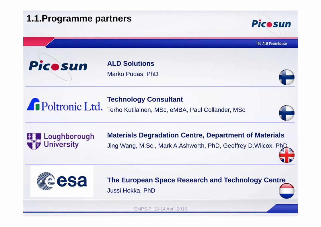
1.1.Programme partners
EMPS-7, 13-14 April 2016
ALD SolutionsMarko Pudas, PhD
Technology ConsultantTerho Kutilainen, MSc, eMBA, Paul Collander, MSc
Materials Degradation Centre, Department of MaterialsJing Wang, M.Sc., Mark A.Ashworth, PhD, Geoffrey D.Wilcox, PhD
The European Space Research and Technology CentreJussi Hokka, PhD
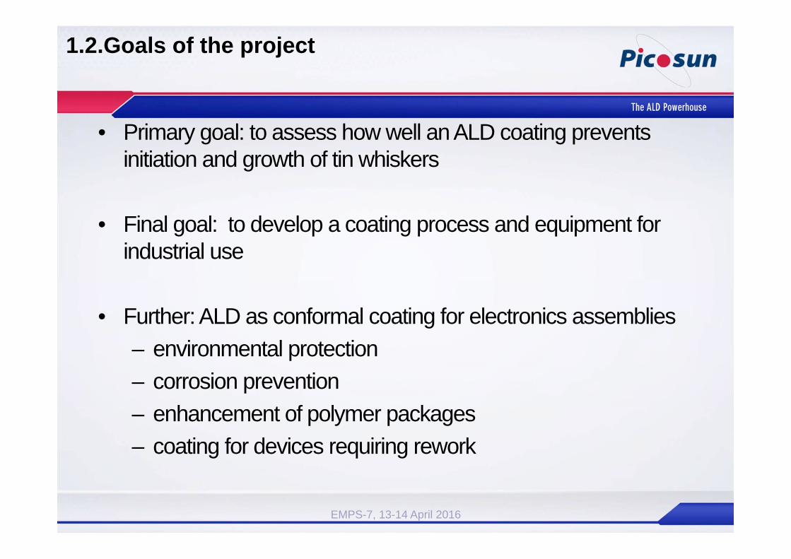
1.2.Goals of the project
• Primary goal: to assess how well an ALD coating prevents initiation and growth of tin whiskers
• Final goal: to develop a coating process and equipment for industrial use
• Further: ALD as conformal coating for electronics assemblies– environmental protection– corrosion prevention– enhancement of polymer packages– coating for devices requiring rework
EMPS-7, 13-14 April 2016
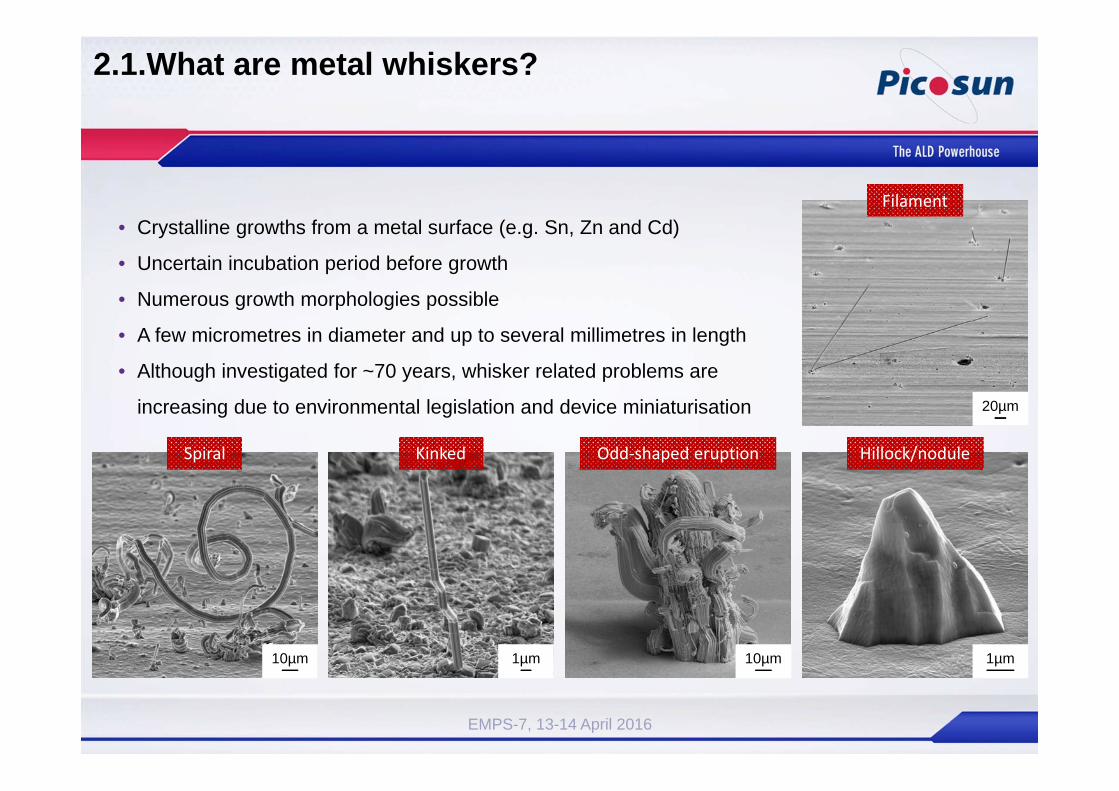
• Crystalline growths from a metal surface (e.g. Sn, Zn and Cd)
• Uncertain incubation period before growth
• Numerous growth morphologies possible
• A few micrometres in diameter and up to several millimetres in length
• Although investigated for ~70 years, whisker related problems are
increasing due to environmental legislation and device miniaturisation
10µm 1µm10µm
20µm
Filament
Hillock/noduleOdd‐shaped eruptionSpiral Kinked
1µm
2.1.What are metal whiskers?
EMPS-7, 13-14 April 2016
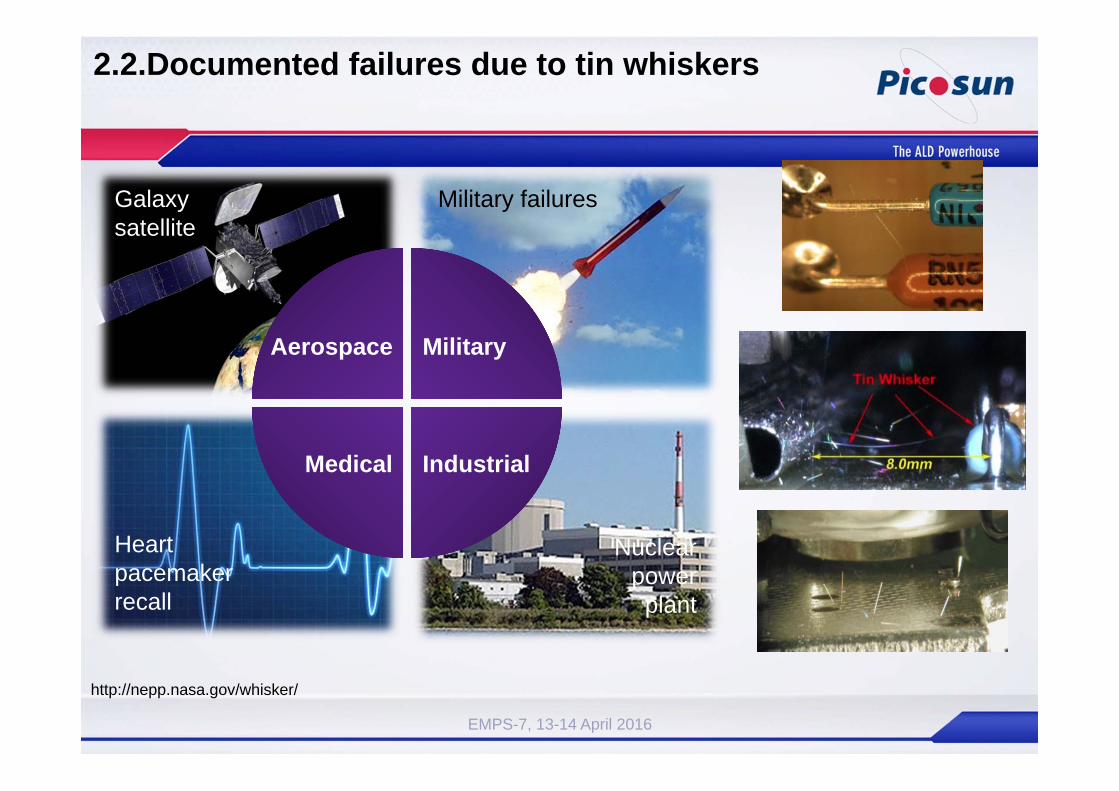
Aerospace Military
Medical Industrial
Galaxy satellite
Military failures
Heart pacemaker recall
Nuclear power
plant
2.2.Documented failures due to tin whiskers
http://nepp.nasa.gov/whisker/
EMPS-7, 13-14 April 2016
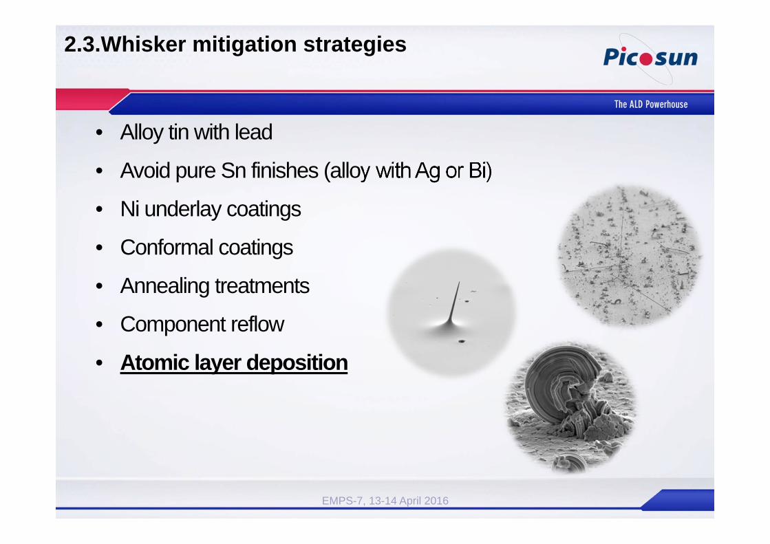
2.3.Whisker mitigation strategies
• Alloy tin with lead
• Avoid pure Sn finishes (alloy with Ag or Bi)
• Ni underlay coatings
• Conformal coatings
• Annealing treatments
• Component reflow
• Atomic layer deposition
EMPS-7, 13-14 April 2016
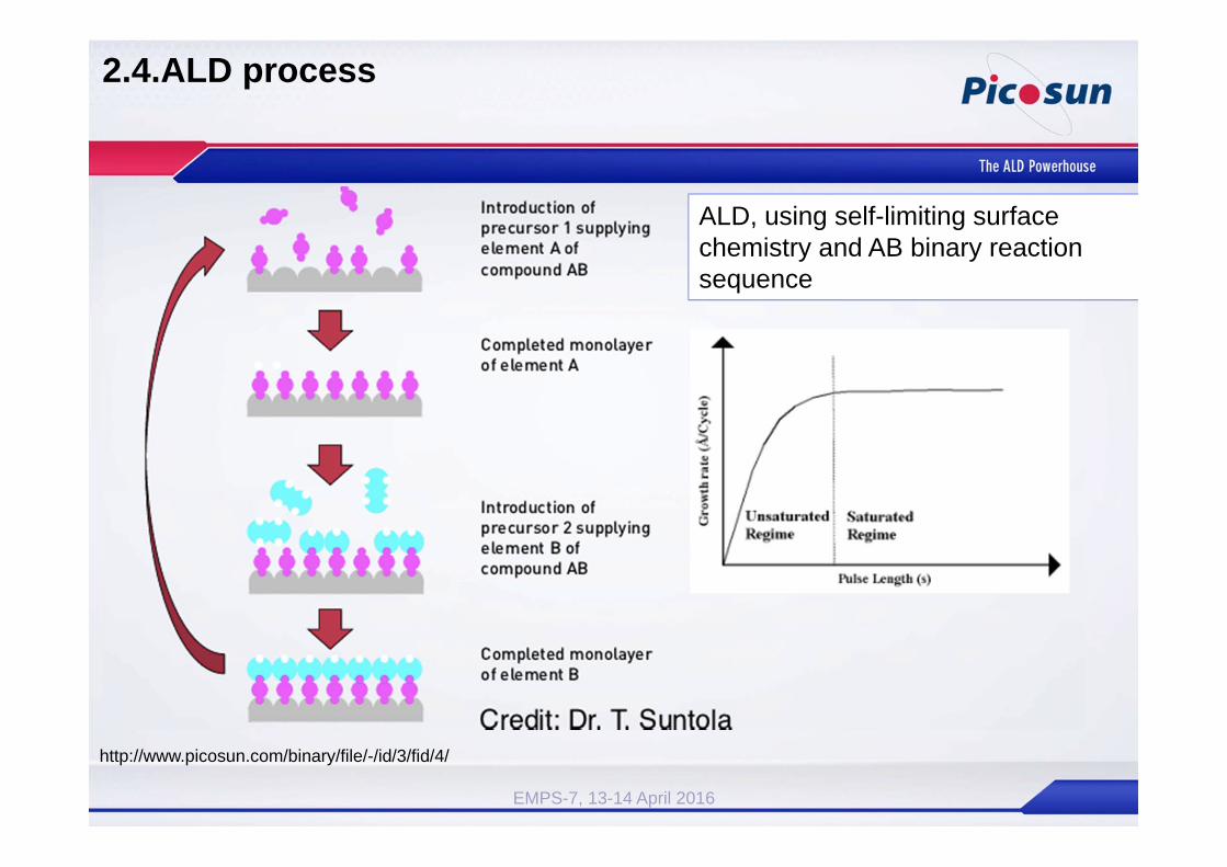
2.4.ALD process
EMPS-7, 13-14 April 2016
ALD, using self-limiting surface chemistry and AB binary reaction sequence
http://www.picosun.com/binary/file/-/id/3/fid/4/
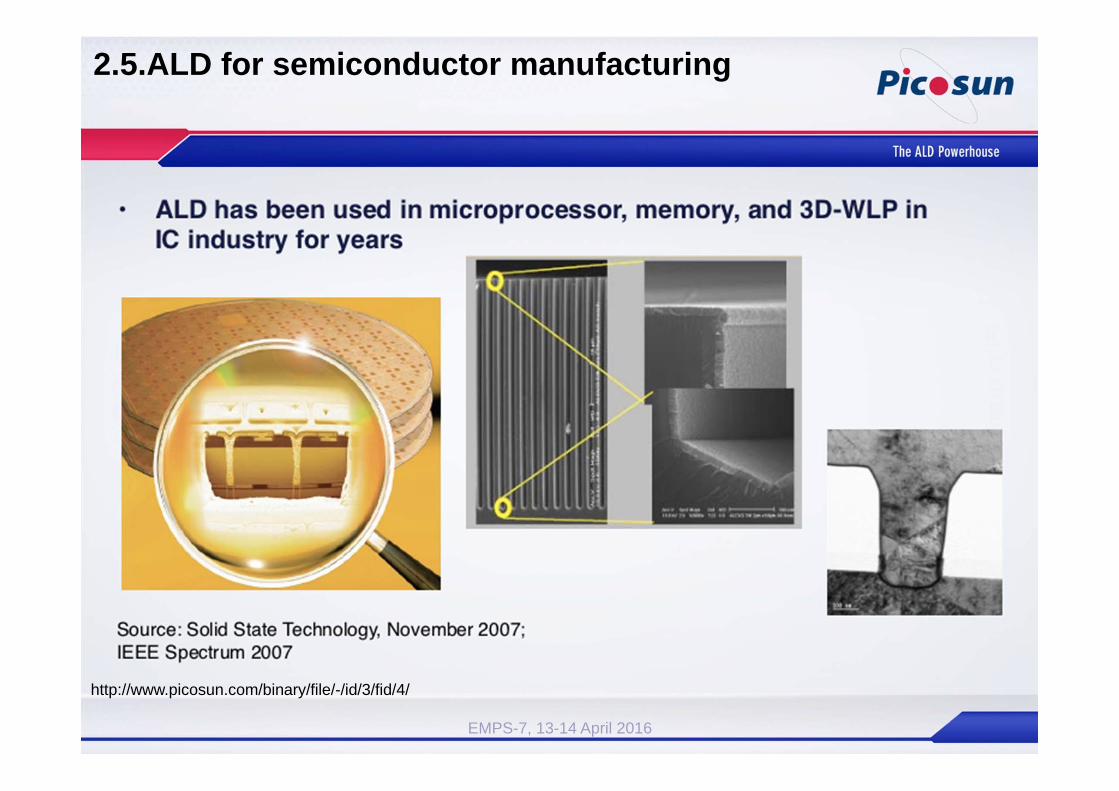
2.5.ALD for semiconductor manufacturing
EMPS-7, 13-14 April 2016
http://www.picosun.com/binary/file/-/id/3/fid/4/
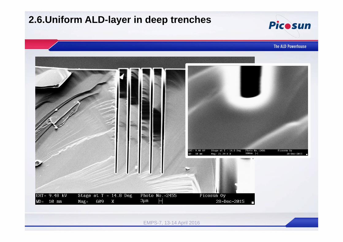
2.6.Uniform ALD-layer in deep trenches
EMPS-7, 13-14 April 2016
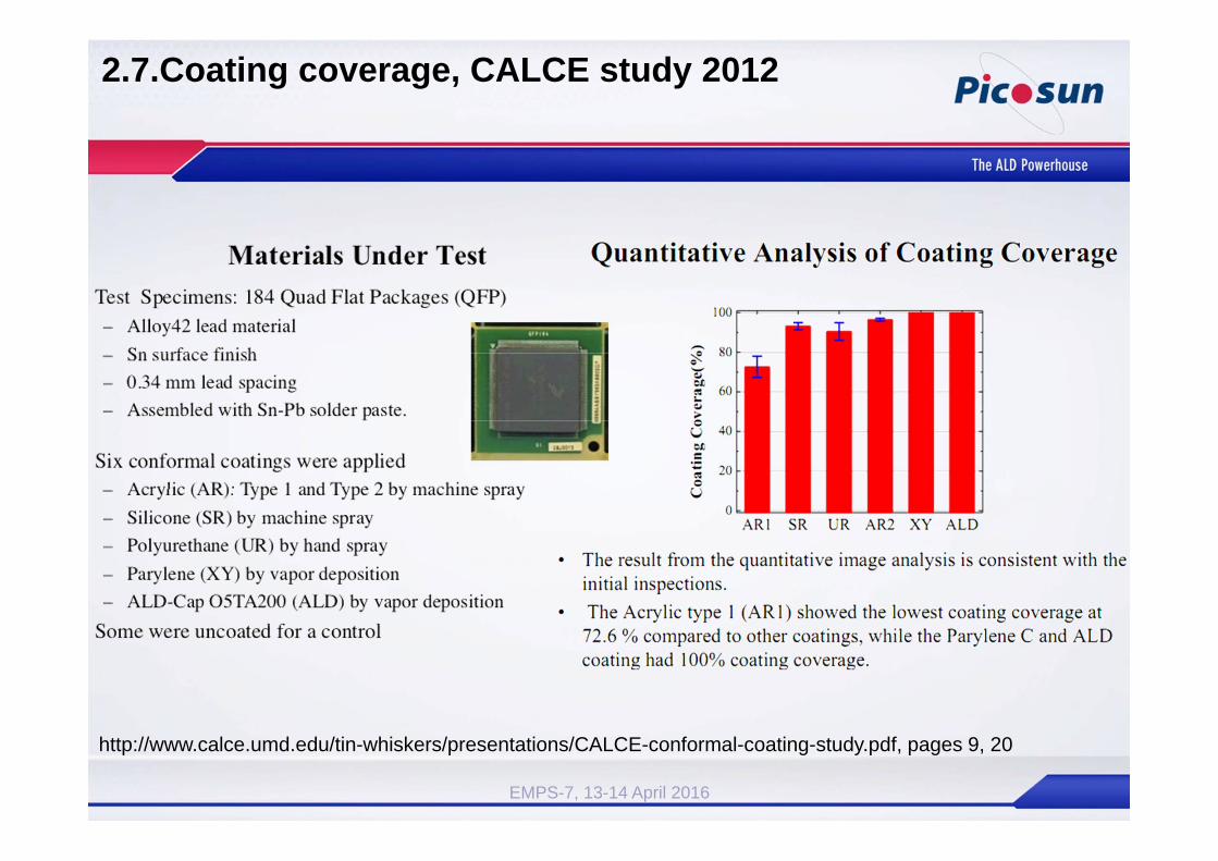
2.7.Coating coverage, CALCE study 2012
EMPS-7, 13-14 April 2016
http://www.calce.umd.edu/tin-whiskers/presentations/CALCE-conformal-coating-study.pdf, pages 9, 20
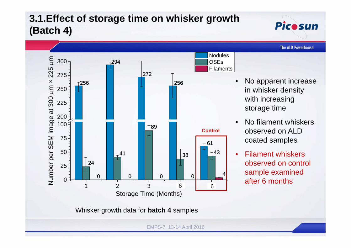
• No apparent increase in whisker density with increasing storage time
• No filament whiskers observed on ALD coated samples
• Filament whiskers observed on control sample examined after 6 months
Whisker growth data for batch 4 samples
256
294
272256
61
24
41
89
38 43
0 0 0 0 4
256
294
272256
61
24
41
89
38 43
0 0 0 0 4
1 2 3 4 50
25
50
75
100200
225
250
275
300
6Num
ber p
er S
EM
imag
e at
300
m
× 2
25
m
Storage Time (Months)
Nodules OSEs Filaments
6
Control
EMPS-7, 13-14 April 2016
3.1.Effect of storage time on whisker growth (Batch 4)
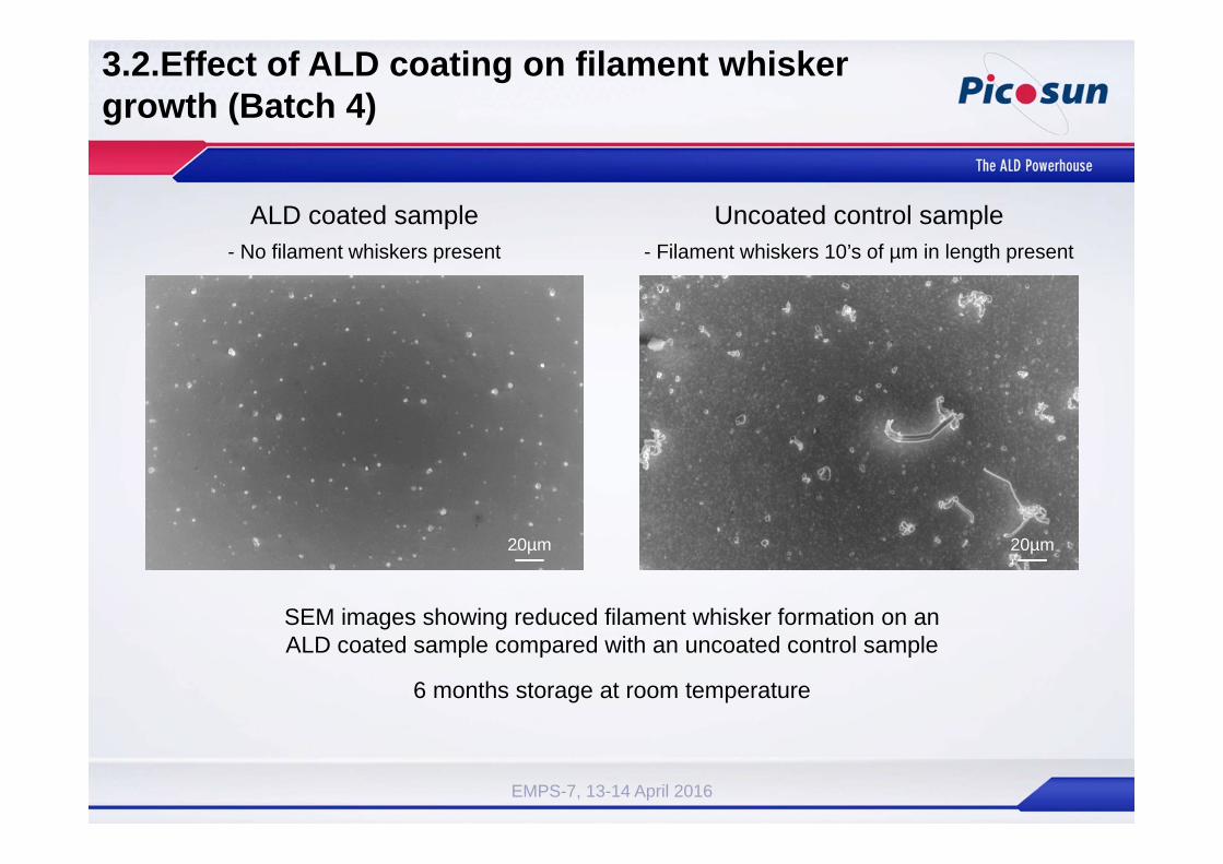
SEM images showing reduced filament whisker formation on an ALD coated sample compared with an uncoated control sample
6 months storage at room temperature
ALD coated sample- No filament whiskers present
Uncoated control sample- Filament whiskers 10’s of µm in length present
3.2.Effect of ALD coating on filament whisker growth (Batch 4)
20µm20µm
EMPS-7, 13-14 April 2016
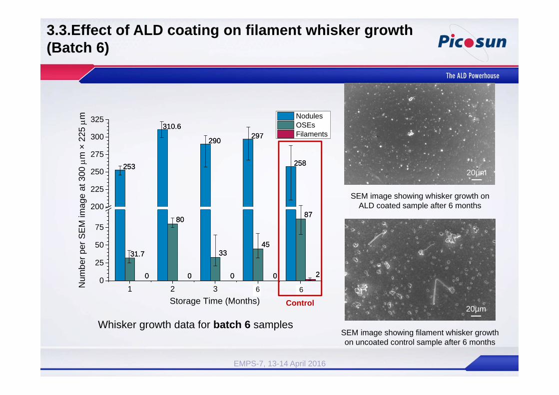
SEM image showing whisker growth on ALD coated sample after 6 months
SEM image showing filament whisker growth on uncoated control sample after 6 months
20µm
20µm
Whisker growth data for batch 6 samples
253
310.6
290 297
258
31.7
80
3345
87
0 0 0 0 2
253
310.6
290 297
258
31.7
80
3345
87
0 0 0 0 2
1 2 3 4 50
25
50
75
200
225
250
275
300
325
Num
ber p
er S
EM
imag
e at
300
m
× 2
25
m
Storage Time (Months)
Nodules OSEs Filaments
6 6
Control
EMPS-7, 13-14 April 2016
3.3.Effect of ALD coating on filament whisker growth (Batch 6)
20µm
20µm
SEM image showing whisker growth on ALD coated sample after 6 months
SEM image showing filament whisker growth on uncoated control sample after 6 months
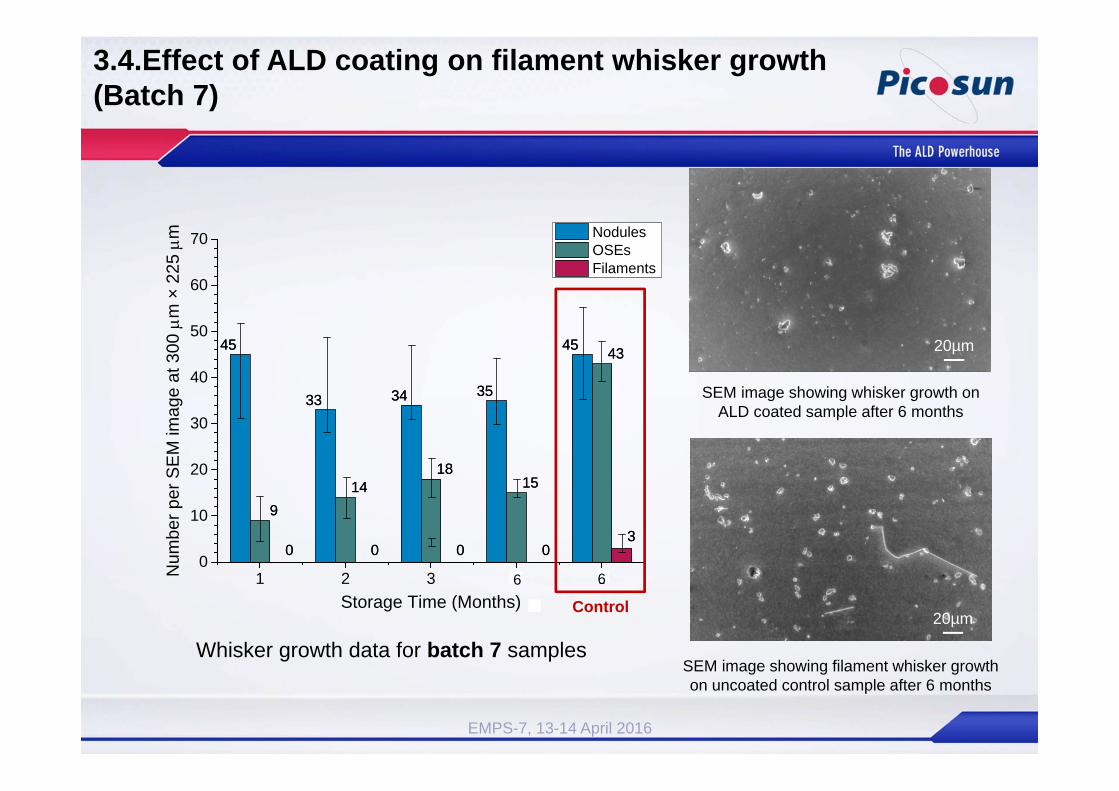
Whisker growth data for batch 7 samples
45
33 34 35
45
914
1815
43
0 0 0 03
45
33 34 35
45
914
1815
43
0 0 0 03
1 2 3 4 50
10
20
30
40
50
60
70
Num
ber p
er S
EM
imag
e at
300
m
× 2
25
m
Storage Time (Months)
Nodules OSEs Filaments
6 6
Control
EMPS-7, 13-14 April 2016
3.4.Effect of ALD coating on filament whisker growth (Batch 7)
20µm
20µm
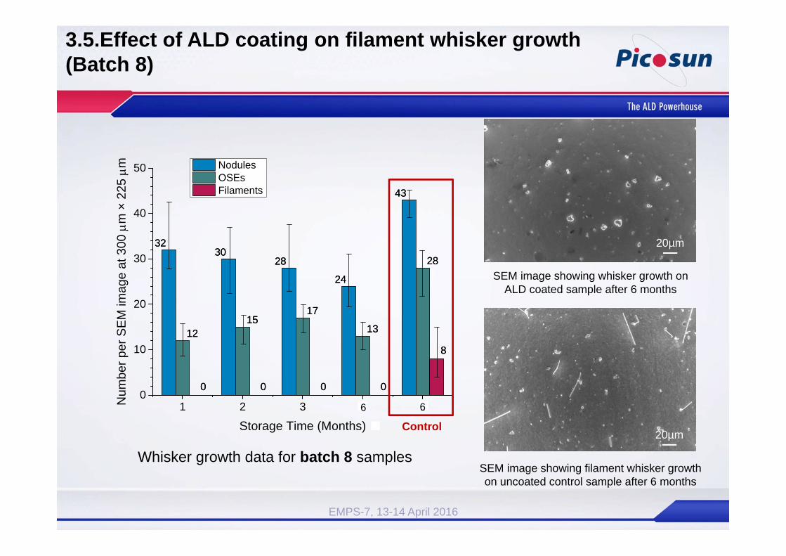
SEM image showing whisker growth on ALD coated sample after 6 months
SEM image showing filament whisker growth on uncoated control sample after 6 months
Whisker growth data for batch 8 samples
3230
28
24
43
1215
17
13
28
0 0 0 0
8
3230
28
24
43
1215
17
13
28
0 0 0 0
8
1 2 3 4 50
10
20
30
40
50
Num
ber p
er S
EM
imag
e at
300
m
× 2
25
m
Storage Time (Months)
Nodules OSEs Filaments
6 6
Control
EMPS-7, 13-14 April 2016
3.5.Effect of ALD coating on filament whisker growth (Batch 8)
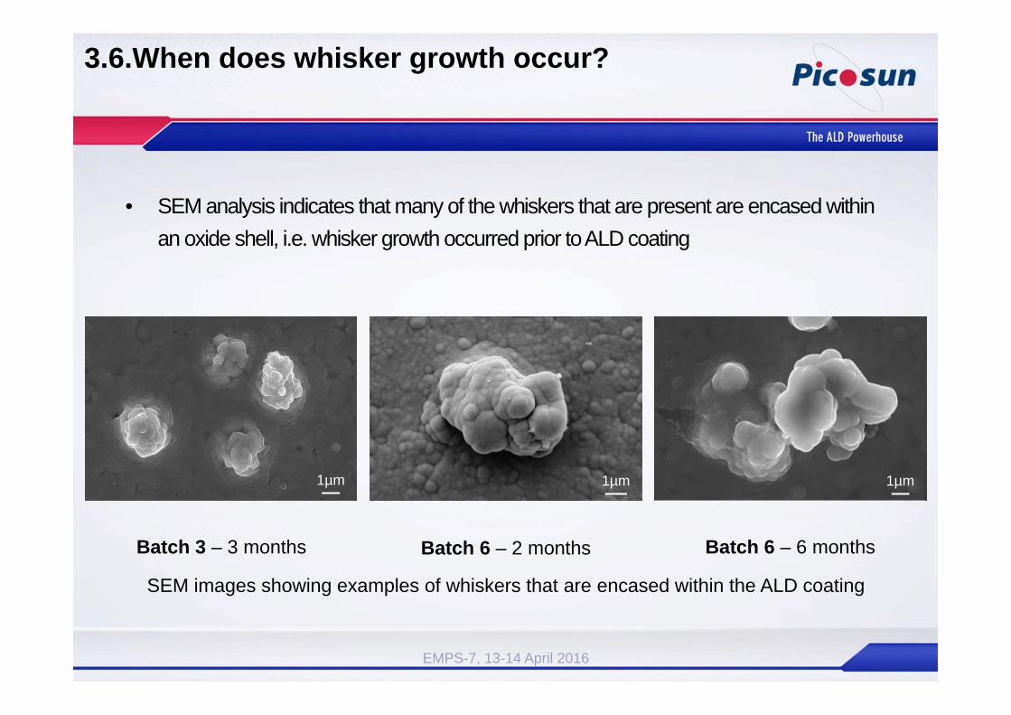
3.6.When does whisker growth occur?
• SEM analysis indicates that many of the whiskers that are present are encased within an oxide shell, i.e. whisker growth occurred prior to ALD coating
Batch 3 – 3 months Batch 6 – 2 months Batch 6 – 6 months
SEM images showing examples of whiskers that are encased within the ALD coating
1µm1µm 1µm
EMPS-7, 13-14 April 2016
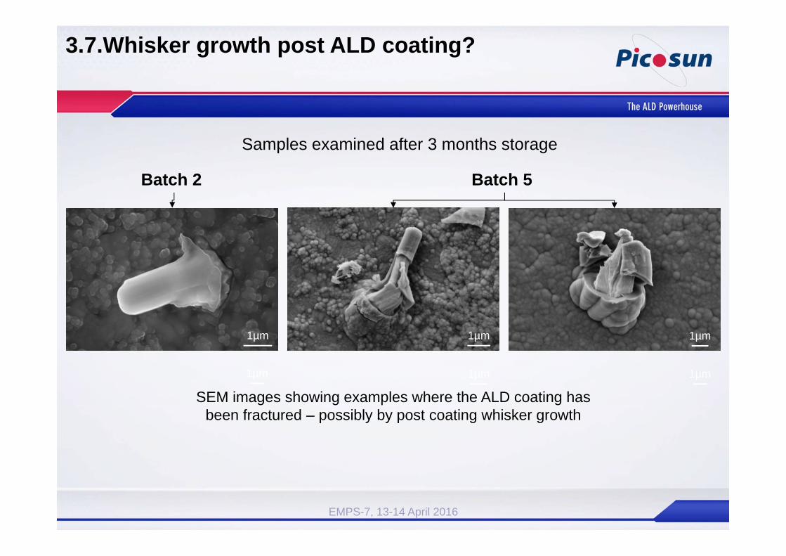
3.7.Whisker growth post ALD coating?
1µm1µm 1µm
EMPS-7, 13-14 April 2016
SEM images showing examples where the ALD coating has been fractured – possibly by post coating whisker growth
Samples examined after 3 months storage
Batch 5 Batch 2
1µm1µm1µm
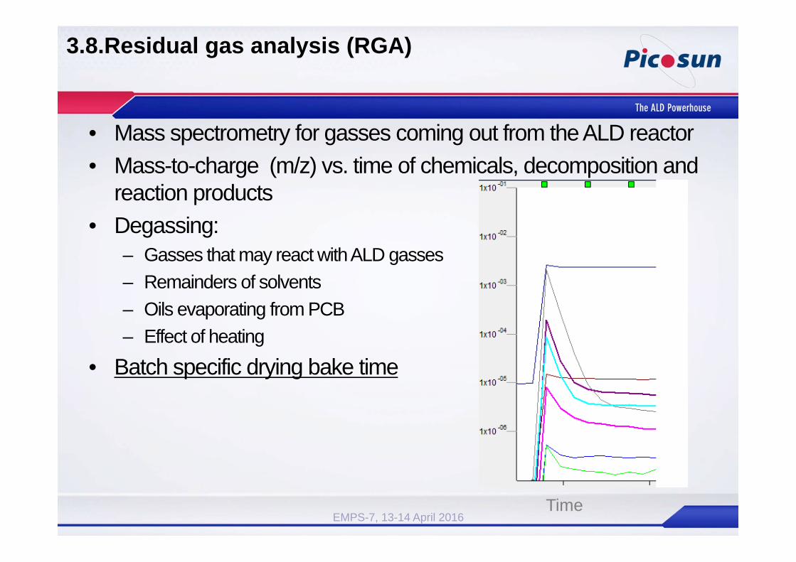
3.8.Residual gas analysis (RGA)
• Mass spectrometry for gasses coming out from the ALD reactor• Mass-to-charge (m/z) vs. time of chemicals, decomposition and
reaction products• Degassing:
– Gasses that may react with ALD gasses– Remainders of solvents– Oils evaporating from PCB– Effect of heating
• Batch specific drying bake time
EMPS-7, 13-14 April 2016Time
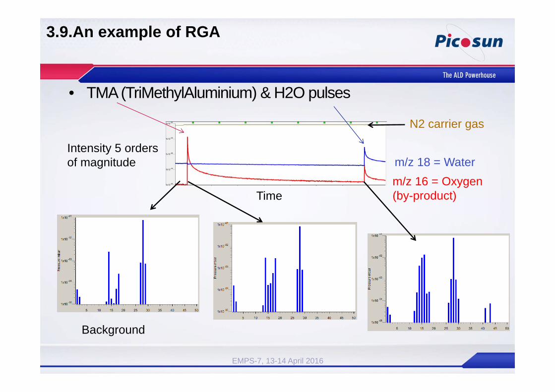
3.9.An example of RGA
• TMA (TriMethylAluminium) & H2O pulses
EMPS-7, 13-14 April 2016
Intensity 5 orders of magnitude
Time
N2 carrier gas
m/z 16 = Oxygen(by-product)
m/z 18 = Water
Background
4.1.Summary
• The density and length of filament type whiskers is greater in unprocessed control samples than those that have undergone ALD coating
• Filament whiskers, typically 10’s of µm in length, are present on all the control samples analysed at the 6 month interval
• In general, whisker densities do not appreciably increase with increased storage time for the ALD processed samples
• SEM analysis suggests that whiskers had developed on the samples prior to ALD coating
• Printed circuits boards contain various substances requiring special attention in ALD process
EMPS-7, 13-14 April 2016
5.1.Questions?
Picosun Oy (www.picosun.com)
Picosun Oy, a limited liability company registered in Finland, is a leading provider of high quality
ALD coating equipment and solutions to global industries. Picosun has over four decades of
unparalleled, groundbreaking experience in the field ofALD, reaching back to the invention of the
technology itself. Today, PICOSUN™ALD systems are in production use in many of the world’s
largest microelectronics, sensor, semiconductor and various other industries. Picosunheadquarters is located in Espoo, Finland and its production facilities in Masala, Finland. Picosunhas subsidiaries in North America, Singapore, China, Japan, and Taiwan, and world-wide salesand support network.
EMPS-7, 13-14 April 2016

![Metal Oxide Thin Films and Nanostructures Made by ALD · mands is atomic layer deposition (ALD)[9,10]. ALD, also known as atomic layer epitaxy (ALE) or atomic layer chemical vapour](https://img.pdfslide.us/doc/110x75/60af0a63ec0db37505778719/metal-oxide-thin-films-and-nanostructures-made-by-ald-mands-is-atomic-layer-deposition.jpg)


![Atomic layer deposition onto polymer surfaces · Atomic layer deposition (ALD) is a layer-by-layer process based on self-limiting gas-solid surface reactions [1-3]. Deposition cycles](https://img.pdfslide.us/doc/110x75/5f70f4ce86c8b13d2031a5ca/atomic-layer-deposition-onto-polymer-surfaces-atomic-layer-deposition-ald-is-a.jpg)