Embed Size (px)
DESCRIPTION
aom procesor
Citation preview

Doc. # 323431-001
Intel® Atom™ Processor N450, D410 and D510 with the Intel® 82801HM I/O Controller Hub
Development Kit User’s Manual
February 2010

2 Doc. # 323431-001
INFORMATION IN THIS DOCUMENT IS PROVIDED IN CONNECTION WITH INTEL® PRODUCTS. NO LICENSE, EXPRESS OR IMPLIED, BY ESTOPPEL OR OTHERWISE, TO ANY INTELLECTUAL PROPERTY RIGHTS IS GRANTED BY THIS DOCUMENT. EXCEPT AS PROVIDED
IN INTEL'S TERMS AND CONDITIONS OF SALE FOR SUCH PRODUCTS, INTEL ASSUMES NO LIABILITY WHATSOEVER, AND INTEL DISCLAIMS ANY EXPRESS OR IMPLIED WARRANTY, RELATING TO SALE AND/OR USE OF INTEL PRODUCTS INCLUDING LIABILITY OR
WARRANTIES RELATING TO FITNESS FOR A PARTICULAR PURPOSE, MERCHANTABILITY, OR INFRINGEMENT OF ANY PATENT, COPYRIGHT OR OTHER INTELLECTUAL PROPERTY RIGHT.
UNLESS OTHERWISE AGREED IN WRITING BY INTEL, THE INTEL PRODUCTS ARE NOT DESIGNED NOR INTENDED FOR ANY
APPLICATION IN WHICH THE FAILURE OF THE INTEL PRODUCT COULD CREATE A SITUATION WHERE PERSONAL INJURY OR DEATH MAY OCCUR.
Intel may make changes to specifications and product descriptions at any time, without notice. Designers must not rely on the
absence or characteristics of any features or instructions marked "reserved" or "undefined." Intel reserves these for future definition and shall have no responsibility whatsoever for conflicts or incompatibilities arising from future changes to them. The information
here is subject to change without notice. Do not finalize a design with this information.
The products described in this document may contain design defects or errors known as errata which may cause the product to deviate from published specifications. Current characterized errata are available on request.
Intel® High Definition Audio requires a system with an appropriate Intel chipset and a motherboard with an appropriate codec and
the necessary drivers installed. System sound quality will vary depending on actual implementation, controller, codec, drivers and speakers. For more information about Intel® HD audio, refer to http://www.intel.com/.
Contact your local Intel sales office or your distributor to obtain the latest specifications and before placing your product order.
This document contains information on products in the design phase of development.
Intel, the Intel logo, the Intel Atom family, and Intel HD Audio are trademarks of Intel Corporation in the U.S. and other countries.
*Other names and brands may be claimed as the property of others.
Copyright © 2010 Intel Corporation. All rights reserved.
Doc. # 323431-001 3
Contents
1 Introduction ................................................................................................... 7
1.1 Content Overview ................................................................................. 8 1.2 Terminology ........................................................................................ 8 1.3 Technical Support ................................................................................. 9
1.3.1 Additional Technical Support .................................................... 10 1.4 Product Literature ............................................................................... 10 1.5 Related Documents ............................................................................. 10
2 Development Kit Contents .............................................................................. 12
2.1 Included Hardware and Documentation .................................................. 12 2.2 Software Key Features......................................................................... 12 2.3 EFI Firmware ..................................................................................... 13 2.4 Before You Begin ................................................................................ 13
3 Evaluation Board Features .............................................................................. 15
3.1 Major Features ................................................................................... 18 3.2 Processor Support............................................................................... 20
3.2.1 Processor Voltage Regulators ................................................... 20 3.3 Subsystem Descriptions ....................................................................... 21
3.3.1 Processor Features: ................................................................ 21 3.3.2 Intel® 82801HM I/O Controller ................................................ 22 3.3.3 System Memory..................................................................... 22 3.3.4 Display................................................................................. 22 3.3.5 PCI Express* Slots ................................................................. 23 3.3.6 Soft Audio/Soft Modem ........................................................... 23 3.3.7 SATA Storage ........................................................................ 23 3.3.8 PATA Storage ........................................................................ 23 3.3.9 USB Connectors ..................................................................... 23 3.3.10 LPC Slot ............................................................................... 24 3.3.11 Super I/O (SIO)..................................................................... 24 3.3.12 EFI SPI Flash Device ............................................................... 24 3.3.13 Trusted Platform Module (TPM) Header ...................................... 24 3.3.14 Clocks .................................................................................. 24 3.3.15 Real Time Clock ..................................................................... 24 3.3.16 In-Target Probe (ITP) and Debug Support .................................. 24 3.3.17 Power Supply Solution ............................................................ 25 3.3.18 Board Size ............................................................................ 25
4 Board Power Management .............................................................................. 26
4.1 Power Measurement Support ................................................................ 26
5 Evaluation Board Feature Locations .................................................................. 29
5.1 Evaluation Board Features .................................................................... 30 5.2 PCI Express* Slots and Mini Card Connectors .......................................... 30
4 Doc. # 323431-001
5.3 Connectors ........................................................................................ 31 5.3.1 Back Panel Connectors ............................................................ 31 5.3.2 PS/2 Connectors .................................................................... 32 5.3.3 USB Connectors ..................................................................... 32 5.3.4 Video Connector .................................................................... 32
5.4 Configuration Settings ......................................................................... 32 5.4.1 Configuration Jumpers/Switches ............................................... 32 5.4.2 Manual VID Support for CPU .................................................... 35
5.5 Power On and Reset Push Buttons ......................................................... 35 5.6 LEDs ................................................................................................ 35 5.7 Headers ............................................................................................ 38
5.7.1 SPI Programming Headers ....................................................... 38 5.7.2 ATX Switch/LED Front Panel Header .......................................... 38 5.7.3 USB Front Panel Header .......................................................... 39 5.7.4 TPM Header .......................................................................... 39
6 Quick Start .................................................................................................. 41
6.1 Required Peripherals ........................................................................... 41 6.2 Power Up /Power Down........................................................................ 41
6.2.1 Pre-Power Up ........................................................................ 41 6.2.2 Powering Up the Board ........................................................... 42 6.2.3 Powering Down the Board ....................................................... 43
6.3 Firmware Updates ............................................................................... 43
Appendix A Daughter and Plug-In Cards ............................................................................ 44
A.1 Mott Canyon 4 Interposer Card ............................................................. 44 A.1.1 Jumper Settings .................................................................... 45 A.1.2 Audio Firmware Configuration .................................................. 47
Appendix B Intel® MVP-6 VID Codes ................................................................................. 48
Appendix C VRD11 VID Codes ......................................................................................... 51
Appendix D PCI Express* Ports ........................................................................................ 54
D.1 Configuring PCI Express* Ports ............................................................. 54
Appendix E Development Kit Chassis Features.................................................................... 58
E.1 External Feature Locations ................................................................... 58 E.1.1 Front of Chassis ..................................................................... 59 E.1.2 Rear of Chassis...................................................................... 60
E.2 Internal Components ........................................................................... 61 E.3 Accessing the Board ............................................................................ 61
Doc. # 323431-001 5
Figures
Figure 1. Evaluation Board Block Diagram ......................................................... 15 Figure 2. Evaluation Board (Top View) .............................................................. 16 Figure 3. Evaluation Board (Bottom View w/SODIMMs) ........................................ 17 Figure 4. Evaluation Board Feature Placement Overview ...................................... 30 Figure 5. Back Panel Connectors ...................................................................... 31 Figure 6. Location of the Configuration Jumpers/Switches .................................... 33 Figure 7. Board LEDs ..................................................................................... 37 Figure 8. Board Headers ................................................................................. 38 Figure 9. Mott Canyon 4 Interposer Card ........................................................... 45 Figure 10. PCI Express* Configuration Block Diagram with Default Configuration ..... 54 Figure 11. Front of Chassis ............................................................................ 59 Figure 12. Rear of Chassis .............................................................................. 60 Figure 13. Internal Components of Development Kit ............................................ 61 Figure 14. Motherboard Tray Removal .............................................................. 62 Figure 15. Chassis with Open Motherboard Tray ................................................. 63
Tables
Table 1. Intel® Literature Centers .................................................................... 10 Table 2. Related Documents............................................................................ 11 Table 3. Evaluation Board Feature Set Summary ................................................ 18 Table 4. Power Measurement Resistor ............................................................... 26 Table 5. Digital Multi-Meter Comparison ............................................................ 26 Table 6: Comparison of Agilent 34401A* and Fluke 79* Digital Multi-Meters ........... 27 Table 7. Board Voltage Rails ........................................................................... 27 Table 8. Back Panel Connectors ....................................................................... 31 Table 9. Configuration Jumper/Switches Settings ................................................ 33 Table 10. Board LEDs..................................................................................... 35 Table 11. ATX Switch/LED Front Panel Header .................................................... 39 Table 12. USB Front Panel Header .................................................................... 39 Table 13. TPM Header .................................................................................... 39 Table 14. Mott Canyon 4 Interposer Card Configuration Jumper/Switches ............... 46 Table 15. Voltage Identification Definition ......................................................... 48 Table 16. Voltage Identification Definition ......................................................... 51 Table 17. PCIe Slot Configurations ................................................................... 55 Table 18. PCIe Route Groups .......................................................................... 55 Table 19. PCIe Group Resistors........................................................................ 55 Table 20. All PCIe Resistors ............................................................................ 56 Table 21. PCIe Straps .................................................................................... 56

6 Doc. # 323431-001
Revision History
Document Number
Revision Number
Description Revision Date
323431 001 Initial public release of this document. February 2010
§

Introduction
Doc. # 323431-001 7
1 Introduction
This manual describes the typical hardware set-up procedures, features, and use of the evaluation board and other components included in the Intel® Atom™ Processor N450, D410 and D510 with the Intel® 82801HM I/O Controller Hub Development Kit.
This manual is written for OEMs, system evaluators, and embedded system developers. This document defines all jumpers, headers, LED functions, and their locations on the development board along with subsystem features. This manual assumes basic familiarity with the fundamental concepts involved with installing and configuring hardware for a personal computer system.
There are two different development kits offered featuring the Intel® Atom™ Processor Family with Intel® 82801HM I/O Controller Hub:
Intel® Atom™ Processor N450 (single core, 5.5 watts) with Intel® 82801HM I/O Controller Development Kit
Intel® Atom™ processor D510 (dual core, 13 watts total) with Intel® 82801HM I/O Controller Development Kit
There are three Development Kit Boards for this platform. They are designed with the Intel® Embedded Flexible Design guidelines and will be populated with one of the following configurations:
Intel® Atom™ Processor N450 with Intel® 82801HM I/O Controller
Intel® Atom™ Processor D410 with Intel® 82801HM I/O Controller
Intel® Atom™ Processor D510 with Intel® 82801HM I/O Controller
Read this document in its entirety prior to applying power to the motherboard. Intel recommends having both the schematic and board present while reading this document.
The references in this document correlate to reference designators and board properties of Intel® Atom™ Processor N450, D410 and D510 with the Intel® 82801HM I/O Controller Hub FAB D and FAB E Customer Reference Boards.
This manual is intended to be used with the development kit but can also be used to help bring up a Intel® Atom™ Processor N450, D410 and D510 with the Intel® 82801HM I/O Controller Hub Customer Reference Board, although not all associated peripherals will be included with the board.
Introduction
8 Doc. # 323431-001
1.1 Content Overview
Chapter 1, ―Introduction‖: Explains the content available in the document, key terminology, where to get product literature and related documents.
Chapter 2, ―Development Kit Contents‖: Outlines the hardware and software included with the Kit as well as any needed hardware for using the kit.
Chapter 3, ―Evaluation Board Features‖: Describes the many features of the board.
Chapter 4, ―Evaluation Board Power Management‖: Offers power calculations and a table of power rails used with the board.
Chapter 5, ―Evaluation Board Feature Locations‖: Points out where various features are located on the board.
Chapter 6, ―Quick Start‖: How to power up and power down the board.
For more information on the Development kit chassis and removing the board please see Appendix E.
1.2 Terminology
Term Definition
ACPI Advanced Configuration Power Interface
BGA Ball Grid Array
DDR Double Data Rate
DMA Direct Memory Access
EFI Extensible Firmware Interface
FAE Field Application Engineer
FSB Front Side Bus
FWH Firmware Hub
GPIO General Purpose Input Output
IDE Integrated Device Electronics
IEGD Intel® Embedded Graphics Driver
IMVP Intel® Mobile Voltage Positioning
Intel® HD Audio Intel® High Definition Audio
Mott Canyon 4 This Add-in Card enables Intel® HD Audio functionality
ITP In-Target Probe
JEDEC Joint Electron Device Engineering Council

Introduction
Doc. # 323431-001 9
Term Definition
KBC Keyboard Controller
LAN Local Area Network
LED Light Emitting Diode
LPC Low Pin Count
LVDS Low Voltage Differential Signaling
MDC Mobile Daughter Card
OS Operating System
PATA Parallel AT Attachment
PC Personal Computer
PCB Printed Circuit Board
PCIe* PCI Express*
PLL Phase Lock Loop
PGA Pin Grid Array
RTC Real Time Clock
SIO Super I/O (Input Output)
SPI Serial Peripheral Interface
SMC System Management Controller
SO-DIMM Small Outline Dual In-line Memory Module
TPM Trusted Platform Module
TSSOP Thin Shrink Small Outline Package
UART Universal Asynchronous Receiver/Transmitter (COM/Serial Port)
USB Universal Serial Bus
VGA Video Graphics Array
VID Voltage Identification
VR Voltage Regulator
VTT Voltage Termination
XDP eXtended Debug Port
1.3 Technical Support
Support Services for your hardware and software are provided through the secure Intel® Premier Support Web site at https://premier.intel.com. Please contact your local Intel representative for access. After you log on, you can obtain technical support, review
Introduction
10 Doc. # 323431-001
―What‘s New,‖ and download any items required to maintain the platform. Support is provided through the following categories:
Intel® AtomTM processor N450, D410, D510/ICH8M (Embedded)
Dev Kit (Embedded/N450, N410, and D510/ICH8M)
BIOS/Firmware Support (Embedded Software)
For issues related to the board, please use the Dev Kit (Embedded/N450, N410, and D510/ICH8M) category.
1.3.1 Additional Technical Support
If you require additional technical support, please contact your field sales representative or local distributor.
1.4 Product Literature
You can order product literature from the following Intel® literature centers.
Table 1. Intel® Literature Centers
U.S and Canada 1-800-548-4725
U.S. (from overseas) 708-296-9333
Europe (U.K.) 44(0)1793-431155
Germany 44(0)1793-421333
France 44(0)1793-421777
Japan (fax only) 81(0)120-47-88-32
Product literature and information can also be found on the web through the following sites:
Intel® Developer Center: http://developer.intel.com/design/index.htm
Intel® Embedded Design Center: http://edc.intel.com/
§
1.5 Related Documents
Table 2 is a partial list of the available collateral. For the complete list, contact your local Intel representative.

Introduction
Doc. # 323431-001 11
Table 2. Related Documents
Document Document Numbers/ Location
Processor and I/O Controller -Related Documents
Intel® Atom™ Processor N450, D410 and D510
with the Intel® 82801HM I/O Controller Platform
Design Guide
Contact your local Intel representative for
the latest revision
Intel® Atom™ Processor N450, D410 and D510
with the Intel® 82801HM I/O Controller Platform
Schematics
Intel® Atom™ Processor N450, D410 and D510
with the Intel® 82801HM I/O Controller Mechanical
and Cadence / OrCad Symbol Files
Intel® Atom™ Processor N400 Series Datasheet
Volumes I & II
Intel® Atom™ Processor D400 and D500 Series
Datasheet Volumes I & II
Intel® Atom™ Processor N400 Series – Sightings Report (SR)
Intel® Atom™ Processor D400 and D500 Series– Sightings Report (SR)
Intel® Atom™ Processor N450, D410 and D510 with the Intel® 82801HM I/O Controller Platform Datasheet Addendum
Intel® I/O Controller Hub 8 (ICH8) Family Datasheet
Intel® I/O Controller Hub (Intel® ICH8M) Specification Update
Firmware-Related Documents
Aptio 4.x Whitepaper www.ami.com/aptio/

Development Kit Contents
12 Doc. # 323431-001
2 Development Kit Contents
2.1 Included Hardware and Documentation
Intel® Atom™ Processor N450, D410 or D510 with the Intel® 82801HM I/O Controller development board (Installed)
Micro ATX chassis with removable motherboard tray
Processor heatsink (Installed)
Jumpers (Installed)
Two 1 GB DDR2 667 SODIMMs (Installed)
Socketed lithium coin cell battery (Installed)
ATX power supply (Installed)
SATA DVD-ROM R/W drive (Installed)
80 GB SATA hard drive (Installed)
Associated cables (Installed)
Mott Canyon 4 Kit with Azalia* HD Audio (Installed)
Documentation and software CD
Note: Not all peripherals listed will be included with an Intel® Atom™ Processor N450, D410 and D510 with the Intel® 82801HM I/O Controller Hub development board if it is not obtained as a development kit.
2.2 Software Key Features
The Development Kit board is pre-loaded with the latest EFI BIOS and the HDD includes a Linux image and needed drivers.
Note: When logging onto the Linux operating system you will need to enter a password. The password is “password.”
The documentation and software CD includes the Development Kit User‘s Manual as well as chipset drivers, LAN drivers, and the GMA Graphics drivers. For Linux, kernels 2.6.30 and beyond have an integrated graphics driver optimized for the Intel® Atom™ Processor N450, D410, and D510. While every care was taken to ensure the latest versions of drivers were provided on the enclosed CD at time of publication, newer revisions may be available. Updated drivers for Intel components can be found at:
http://developer.intel.com/design/intarch/software/index.htm
Development Kit Contents
Doc. # 323431-001 13
For all third-party components, please contact the appropriate vendor for updated drivers.
Note: Software in the kit is provided free by the vendor and is only licensed for evaluation purposes. Refer to the documentation in your evaluation kit for further details on any terms and conditions that may be applicable to the granted licenses. Customers using the tools that work with Microsoft* products must license those products. Any targets created by those tools should also have appropriate licenses. Software included in the kit is subject to change.
Refer to http://developer.intel.com/design/intarch/devkits for details on additional software from other third-party vendors.
2.3 EFI Firmware
This development kit ships with a pre-boot EFI firmware pre-installed. This industry standard EFI firmware runs most standard operating systems, including Microsoft Windows XP*, Microsoft Windows XP Embedded*, Linux, and others.
The following features of the EFI firmware are enabled in the development board:
DDR2 SDRAM detection, configuration, and initialization
Intel® Atom™ Processor N450, D410 and D510 with the Intel® 82801HM I/O Controller Hub configuration
PCI/PCI Express* device enumeration and configuration
Integrated video configuration and initialization
Super I/O configuration
CPU microcode update
For information on updating the firmware please see Section 6.3.
2.4 Before You Begin
The following additional hardware may be necessary to successfully set up and operate the development board.
VGA Monitor: Any standard VGA monitor may be used. The setup instructions in this chapter assume the use of a standard VGA monitor, TV, or flat panel monitor.
Keyboard: The development board can support either a PS/2 or USB style keyboard.
Mouse: The development board can support either a PS/2 or USB style mouse.
Development Kit Contents
14 Doc. # 323431-001
Note: The enclosed driver CD includes drivers necessary for LAN, Integrated graphics, Audio and system INF utilities.
§
Evaluation Board Features
Doc. # 323431-001 15
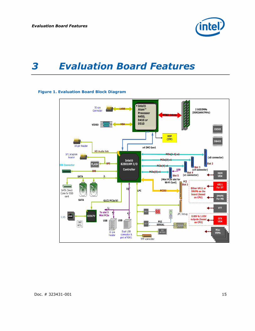
3 Evaluation Board Features
Figure 1. Evaluation Board Block Diagram

Evaluation Board Features
16 Doc. # 323431-001
Figure 2. Evaluation Board (Top View)

Evaluation Board Features
Doc. # 323431-001 17
Figure 3. Evaluation Board (Bottom View w/SODIMMs)
Evaluation Board Features
18 Doc. # 323431-001
3.1 Major Features
Table 3 is a list of the major features for the customer reference board.
Table 3. Evaluation Board Feature Set Summary
Feature Evaluation Board Implementation
Comments
Processor
Note: One of three processor
options is soldered to the board
Intel® Atom™ Processor N450
with integrated graphics/memory
controller, 512KB L2 cache
Or
Intel® Atom™ Processor D410
with integrated graphics/memory
controller, 512KB L2 cache
Or
Intel® Atom™ Processor D510
with integrated graphics/memory
controller, 1MB L2 cache
22 X 22 mm (0.866 x 0.866 inch)
FCBGA package with 0.7 mm (0.0276
inch) ball pitch and 559 balls.
CPU Voltage
Regulator
Note: VR soldered to the board
depends on board processor
Intel® Mobile Voltage Positioning
6 (Intel® MVP6) for Intel®
Atom™ Processor N450
Or
Voltage Regulator Down 11
(VRD11) for Intel® Atom™
Processor D410/D510
1 Phase
Chipset Intel® 82801HM I/O Controller
31 X 31-mm (1.22 x 1.22 inch) FCBGA
package with 1.0-mm and 1.066-mm
(0.0394 inch and 0.0420 inch) ball
pitches and 676-pins.
Board
Technology Type-3 six layer stack-up S-G-Core-S-S-Core-G-S stack-up
Board Size µATX 9.6 x 9.6 inch (243.84 x
243.84 mm) Doubled-sided placement
Memory Two bottom-side SO-DIMM
connectors, single-channel; up to
four ranks total (2/SO-DIMM)
Supports up to 2-GB of system memory
with RAW Card A or C SO-DIMM‘s.
Note: 1GB max per SO-DIMM
Graphics One VGA Connector and one
LVDS Connector No SDVO support.

Evaluation Board Features
Doc. # 323431-001 19
Feature Evaluation Board Implementation
Comments
LVDS options
Single 18-bit LVDS interface;
With Back Light Inverter
(BLI)/LED backlight support
Through a 50-pin cable-up connector
(Panel specific cables required for each
display supported).
Main Clock CK505 (DB403 for PCIe
expansion)
TSSOP, 64-pinspackage
Integrated CK-SSCD
ATA/Storage PATA66/100, 3 SATA
One desktop PATA connector, two
standard SATA connectors, and a SATA
Direct Connector on board edge.
USB 9 USB 2.0 ports
4 back panel connectors
Ports [1:0] and [3:2]
4 cable-up/header
Ports [5:4] and [7:6]
One hard wired to Mini PCIe slot
Port [8]
Soft Audio/ Soft
Modem One Intel® HD Audio MDC Header
Option for 3.3-V and 1.5-V operation
through jumper.
2 x4 for Mott Canyon 4 support
PCI Express*
connectors 3 connectors
1 (x1) connector
1 (x4) connector
1 (x8) connector
Revision 1.0a compliant
NOTE: There are six PCIe lanes, one is only connected to the 82567V Gigabit LAN, another is only
connected to the Mini PCIe slot, and the remaining four can be
configured for different slot
options. Default allows for at least x1 operation on all slots.
NOTE: For more information, refer to Section 2.4.5, PCI Express*
Slots.
PCI Express*
Mini Card
connector
1 connector
1 (x1) Mini PCIe connector with USB
NOTE: For more information, refer to Section 2.4.5, PCI Express* Slots.
LPC One LPC slot for debug 60-pin Slot
TPM WPCT200 or Through TPM header
(TPM 1.2)
SPI SPI based flash with socket 8-pin TSSOP socket with 16-Mbit SPI
SIO WPCD374L Provides power management, floppy,
COM, and PS2 keyboard/mouse.
Evaluation Board Features
20 Doc. # 323431-001
Feature Evaluation Board Implementation
Comments
RTC Battery-backed real time clock
Port 80 Decode Supported down on motherboard
with two seven-segment displays
Power Supply ATX Power Supply ATX 2.01 Power Supply Tested
ITP/AA Support Extended Debug Port (XDP) J9D1 40-pin XDP connector
Power
Management
Form Factor
ACPI Compliant
S0 – Power On
S3 – Suspend to RAM
S4 – Suspend to Disk
S5 – Soft Off
3.2 Processor Support
The reference board supports three different processors, but a particular reference board will be stuffed to support only one of the three different processors. The three processor options include the following:
Intel® Atom™ Processor N450 with integrated graphics/memory controller, 512KB L2 cache
Intel® Atom™ Processor D410 with integrated graphics/memory controller, 512KB L2 cache
Intel® Atom™ Processor D510 with integrated graphics/memory controller, 1MB L2 cache
Each of these processors has a 559-pin FCBGA package. An active heatsink (heatsink plus fan) is installed on the package for use during room temperature ambient operation.
3.2.1 Processor Voltage Regulators
The reference board uses an onboard single-phase regulator for the processor core supply. Each board is populated with a voltage regulator that corresponds to the on board processor.
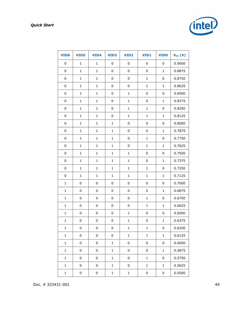
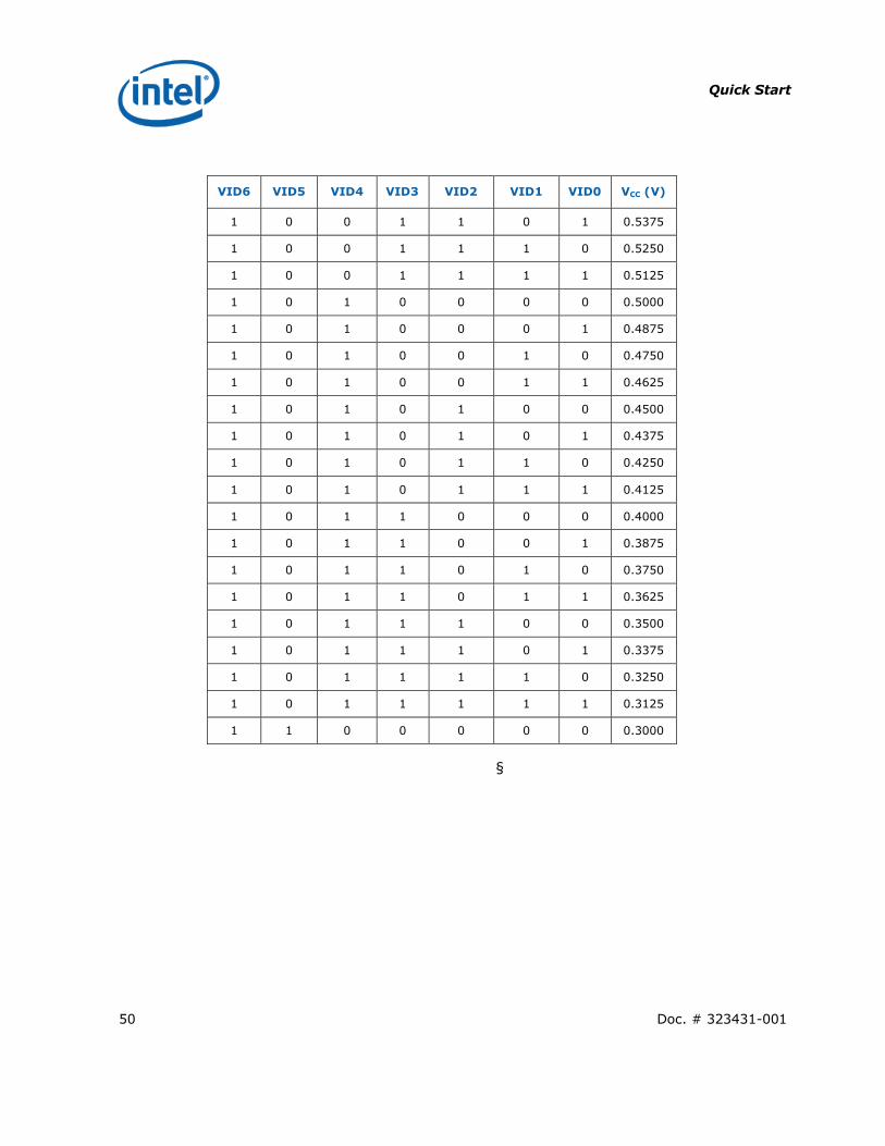
Boards with the Intel® Atom™ Processor N450 use a single-phase voltage regulator that is Intel® Mobile Voltage Positioning 6 (Intel® MVP6) compliant. See Section 4.4.2 for VID jumper location and Appendix B for the VID code table.
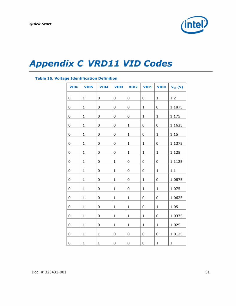
Boards with Intel® Atom™ Processor D410 or D510 use a voltage regulator that is Voltage Regulator Down 11 (VRD11) compliant with a flexible number of phases. See Section 4.4.2 for VID jumper location and Appendix C for the VID code table.

Evaluation Board Features
Doc. # 323431-001 21
3.3 Subsystem Descriptions
Subsystem features refer to the major components and connectors on the evaluation board and their locations. Component and connector locations are labeled with a letter-number combination referencing a grid printed on the edge of every board. Refer to the silkscreen labeling on the evaluation board for details, as well as Figure 4.
3.3.1 Processor Features:
Location: U7E1
3.3.1.1 Intel® Atom™ Processor N450 Processor Features:
Single Core Integrated 1.66 Ghz Intel® Atom™ processor
X4 DMI interface
667MT/s DDR2 Memory Interface
CRT, VGA, Single channel 18-bit LVDS
512 KB cache
Graphics render core frequency @ 200MHz
C0-C4 Power States
Intel® Thermal Monitor support with Adaptive Thermal Monitor 2 enhancement
3.3.1.2 Intel® Atom™ Processor D410 Processor Features:
Single Core Integrated 1.66Ghz Intel® Atom™ processor
X4 DMI interface
667MT/s DDR2 Memory Interface
CRT, VGA, Single channel 18-bit LVDS
512KB cache
Graphics render core frequency @ 400MHz
C0-C1 Power States
Intel® Thermal Monitor support
3.3.1.3 Intel® Atom™ Processor D510 Processor Features:
Dual Core, two integrated 1.66Ghz Intel® Atom™ cores
X4 DMI interface
667MT/s DDR2 Memory Interface
CRT, VGA, Single channel 18-bit LVDS
1 MB cache
Graphics render core frequency @ 400MHz
C0-C1 Power States
Intel® Thermal Monitor support

Evaluation Board Features
22 Doc. # 323431-001
3.3.2 Intel® 82801HM I/O Controller
Location: U4F1
Features:
X4 DMI interface
Six PCI Express* ports, x1 (board offers other PCIe configurations)
Four PCI Rev. 2.3 ports
Ten USB 2.0 compatible ports (Only 9 implemented on board)
One ATAPI-6 (UDMA 100MB/s) IDE channel
Three 3Gb/s SATA Ports
Intel® HD Audio
LPC bus
Serial Peripheral Interface (SPI)
3.3.3 System Memory
Supports two DDR2 SO-DIMMs. SO-DIMMs must be un-buffered and compliant with Raw Cards A or C as defined by JEDEC.
Supports 667-MHz memory bus frequencies.
Location:
SO-DIMM 0 – J3V1
SO-DIMM 1 – J3V2 (populate first)
Note: The Intel® Atom™ Processor N450, D410 and D510 with the Intel® 82801HM I/O Controller Platform Design Guide provides component implementations for SO-DIMM and SO-DIMM/memory down solutions. It is recommended that designs be validated. Contact your Intel Field Representative for access to this document.
3.3.4 Display
The reference board has two options for displaying video:
LVDS – location J9F1
VGA – location J8A1
NOTE: The Intel® Atom™ Processor N450, D410, D510 and the evaluation board only support single channel 18-bit LVDS.
NOTE: The protective tape on top of the Evaluation board LVDS connector must be removed prior to installing an LVDS cable.
NOTE: SDVO is not supported. Customers can use x1 PCI Express*-based discrete, external 2D/3D graphics cards.
Evaluation Board Features
Doc. # 323431-001 23
3.3.5 PCI Express* Slots
Four PCI Express* slots for add-in cards.
o One x8 PCIe Slot (SLOT 2 – J2B1)
o One x4 PCIe Slot (SLOT 3 – J3B1)
o One x1 PCIe Slot (SLOT 4 – J4B3)
o One x1 Mini PCIe Slot (J7W1)
The PCI Express* implementation complies with the PCI Express* Rev. 1.0a specification.
The evaluation board provides one PCI Express* Mini Card form factor slot, and three standard slots of different widths. These slots by default all support x1 devices, while SLOT 2 supports both x1 devices and custom designed x2 devices. In addition to this default configuration, two more options are possible with rework. See Appendix D for details.
3.3.6 Soft Audio/Soft Modem
High Definition Soft Audio/Soft Modem functionality can be enabled through the Mott Canyon 4 daughter card. The evaluation board does not come with an on board Intel® HD Audio codec. The Mott Canyon 4 card is required to enable the High Definition Audio functionality. See Appendix A for more information on the Mott Canyon 4 card.
3.3.7 SATA Storage
The evaluation board provides three SATA connections. One slot is a direct connect type (J2K1), while the other two are standard data connectors (J1H1, J1G1).
3.3.8 PATA Storage
The evaluation board provides only one desktop, 40-pin, PATA66/100 connector (J4K2) that supports master and slave devices.
3.3.9 USB Connectors
The Intel® 82801HM I/O Controller provides ten USB 2.0 ports.
Four ports are routed to the back panel‘s two stacked USB connectors. USB ports [1:0] and [3:2] are routed to the back of the chassis.
Ports [5:4] and [7:6] are routed to the front panel headers (J1E4, J1D1) – See Section 5.7.3.
Port 8 is connected to the Mini PCIe slot (J7W1) on the bottom of the board.
Port 9 is not used on this board.

Evaluation Board Features
24 Doc. # 323431-001
3.3.10 LPC Slot
The LPC Debug slot (J1F1) can be used to debug the SIO, or for adding functionality off the LPC Bus.
3.3.11 Super I/O (SIO)
The Windbond/Nuvoton* WPCD374L SIO (U2F1) serves as multifunction controller for various I/O and power management functions. This controller supports:
Two PS/2 ports (one for mouse, the other for keyboard)
Glue logic
Two serial ports (only one used)
Power sequencing control
3.3.12 EFI SPI Flash Device
A SOIC socket (U4C2) houses the 16-Mbit flash device (P/N# SST25VF016B) that stores the system EFI firmware. The EFI firmware may be programmed through a Microsoft MS-DOS* or Windows*-based utility (See Section 6.3 for details), through the SPI header (J5D1), or externally with proper hardware.
3.3.13 Trusted Platform Module (TPM) Header
The evaluation board implements a header at J1A1 to support TPM 1.2 specification compliant devices.
3.3.14 Clocks
The board uses a CK505 based clock generator in addition to a DB403 clock solution.The BSEL [2:1] signals driven by the processor are used by the CK505 based clock generator to set the internal FSB frequency. The DB403 based clock generator provides additional 100MHz clocks for PCIe ports.
3.3.15 Real Time Clock
An on-board battery maintains power to the real time clock (RTC) when in a mechanical off state (G3 state).
3.3.16 In-Target Probe (ITP) and Debug Support
The board provides on-board ITP support with an XDP connector. Users can debug from the reset vector without EFI or OS dependency (up to OS functionality).

Evaluation Board Features
Doc. # 323431-001 25
Port 80 is also provided as a troubleshooting tool to monitor POST output during firmware execution. See AMI‘s Aptio* site for details of these status codes - http://www.ami.com/aptio/.
3.3.17 Power Supply Solution
The board can be powered from an ATX power supply (desktop solution) that contains all of the voltage regulators necessary to power the system up.
Note: Use an ―ATX12V‖ 2.01 specification compliant power supply regardless of supplier or wattage level. For example, the Sparkle Model No. FSP460-60GLC meets this requirement.
Note: The recommended way to shut down the board is to press and hold the power button switch (S4J1) for 5 seconds until the power supply turns off. Using the power supply switch or pulling the plug out of the wall is not recommended.
Note: If the power switch on the ATX power supply is used to shut down the system, wait at least 5 seconds before turning the system on again.
3.3.18 Board Size
The reference board form factor is similar to the µATX 9.6 x 9.6 inch (243.84 x 243.84 mm) specification. The back panel jacks may not conform to ATX specifications.
§

Board Power Management
26 Doc. # 323431-001
4 Board Power Management
4.1 Power Measurement Support
Power measurement resistors are provided to measure the power on many of the subsystems.
Table 4. Power Measurement Resistor
Feature Value
Tolerance 1%
Value 10 m
NOTE: Intel recommends that larger (~10 m) resistors be stuffed for greater accuracy.
Power on a particular subsystem is calculated using the following formula:
Equation 1.
R
VP
2
R = value of the sense resistor (typically 0.01 Ω)
V = the voltage difference measured across the sense resistor.
Use a high precision digital multi-meter tool such as the Agilent 34401A digital multi-meter. Refer to Table 5 for a comparison of a high-precision, digital multi-meter (Agilent 34401A*) versus a precision, digital multi-meter (Fluke 79*).
Table 5. Digital Multi-Meter Comparison
Example System
Sense Resistor Value 0.01 Ω
Voltage Difference Across Resistor 1.492 mV (149.2 mA)
Calculated Power 0.223 mW

Board Power Management
Doc. # 323431-001 27
Table 6: Comparison of Agilent 34401A* and Fluke 79* Digital Multi-Meters
Agilent 34401A (6½ digit display)
Fluke 79 (3 digit display)
Specification (±0.0030 % of reading)
+ (±0.0030 % of range)
±0.09% ±2 digits
Min Voltage displayed
Calculated power
1.49193 mV
0.22258 mW
1.47 mV
0.216 mW
Max voltage displayed
Calculated power
1.49206 mV
0.22624 mW
1.51 mV
0.228 mW
Error in power ±0.009 % ±0.3 %
NOTE: The precision achieved by using a high precision digital multi-meter versus a normal digital multi-meter is ~33 times more accurate.
Table 7 summarizes all the power measurement sense resistors located on the board. All sense resistors need to be replaced with 0.01 Ω for measurement.
Table 7. Board Voltage Rails
Sch
Pag
e
Co
mp
on
en
t
Vo
ltag
e
Su
pp
ly
Rail
Ref
Des
Resis
tor
(Ω
)
22 PNV
Variable: 0.7-1.2V
(IMVP6 for N450
VRD11 for D410 and
D510) VCC_CPU VCC_CPU_PNV
R8D2,
R8D3,
R8D6
0.00,
1%
22 PNV
0.89 V for Mobile
1.05 V for Desktop VCCGFX VCCGFX_PNV
R7D2,
R7D3
0.00,
1%
22 PNV 1.8 V VCC_DDR VCC_DDR_PNV R7F1,
R7F2
0.00,
1%
23 PNV 1.8 V VCC1P8 VCC1P8_PNV R9E1
0.00,
1%
23 PNV 1.05 V VCC1P05 VCC1P05_PNV
R6E7,
R6E8
0.00,
1%
23 PNV 1.5 V VCC1P5 VCC1P5_PNV R3R1
2
0.00,
1%
23 PNV 3.3 V VCC3P3_PS VCC3P3_PNV R9E3
0.00,
1%
38 ICH 3.3 V VCC3P3_PS VCC3P3_ICH R3F2
0.00,
1%
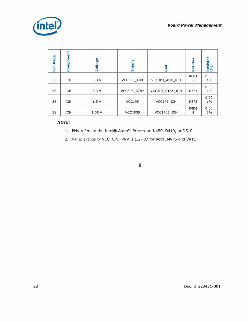
Board Power Management
28 Doc. # 323431-001
Sch
Pag
e
Co
mp
on
en
t
Vo
ltag
e
Su
pp
ly
Rail
Ref
Des
Resis
tor
(Ω
)
38 ICH 3.3 V VCC3P3_AUX VCC3P3_AUX_ICH
R6R1
7
0.00,
1%
38 ICH 3.3 V VCC3P3_STBY VCC3P3_STBY_ICH R3F1 0.00,
1%
38 ICH 1.5 V VCC1P5 VCC1P5_ICH R3F5
0.00,
1%
38 ICH 1.05 V VCC1P05 VCC1P05_ICH
R4D1
8
0.00,
1%
NOTE:
1. PNV refers to the Intel® Atom™ Processor N450, D410, or D510
2. Variable range for VCC_CPU_PNV is 1.2-.07 for both IMVP6 and VR11
§

Evaluation Board Feature Locations
Doc. # 323431-001 29
5 Evaluation Board Feature
Locations
This section contains locations and uses of the various connectors, jumpers, LEDs, headers and other useful components on the board.
Evaluation Board Feature Locations
30 Doc. # 323431-001
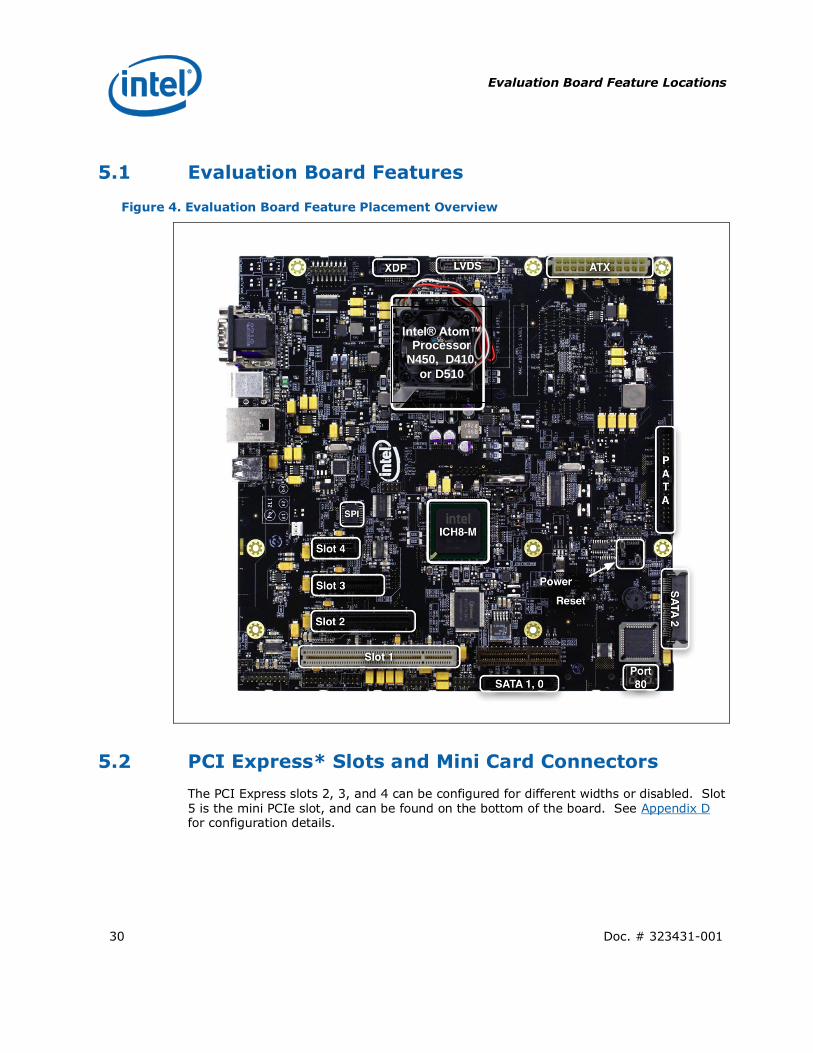
5.1 Evaluation Board Features
Figure 4. Evaluation Board Feature Placement Overview
5.2 PCI Express* Slots and Mini Card Connectors
The PCI Express slots 2, 3, and 4 can be configured for different widths or disabled. Slot 5 is the mini PCIe slot, and can be found on the bottom of the board. See Appendix D for configuration details.
Intel® Atom™ Processor
N450, D410,
or D510

Evaluation Board Feature Locations
Doc. # 323431-001 31
5.3 Connectors
Many of the connectors supply operating voltages up to +5V DC and +12V DC to devices inside the computer chassis, such as fans and internal peripherals.
Caution: Some of these connectors are not over-current protected. A fault in the load presented
by the external devices could damage the board, the interconnecting cable, or the
attached external device if precautions aren‘t taken.
5.3.1 Back Panel Connectors
This section describes the board‘s back panel connectors. Figure 5 shows the location of the connectors on the board, and Table 8 lists the connectors from left to right.
Figure 5. Back Panel Connectors
Table 8. Back Panel Connectors
Ref Des
Of Connector
Description
J8A1 Top: Serial
Bottom: Video
J7A1 Top: Mouse PS/2
Bottom: Keyboard PS/2
J6A1
Top: LAN
Middle: USB 2.0
Bottom: USB 2.0
J5A1 Top: USB 2.0
Bottom: USB 2.0

Evaluation Board Feature Locations
32 Doc. # 323431-001
5.3.2 PS/2 Connectors
PS/2 functionality is included with the SIO device. There are two standard back panel PS/2 connectors (See Figure 5).
5.3.3 USB Connectors
There are four standard back panel USB connectors (See Figure 5). All are USB 2.0 capable.
5.3.4 Video Connector
Video is provided via a female 15-pin standard (D-sub 15) VGA video connector (See Figure 5). There is also LVDS through a 50-pin cable-up connector (See Figure 6).
5.4 Configuration Settings
5.4.1 Configuration Jumpers/Switches
Caution: Do not move jumpers with the power on. Only switches may be moved while power is
on. Always turn off the power and unplug the power cord from the computer before
changing jumper settings. Otherwise, damage to the board could occur.
Figure 6 shows the location of the major configuration jumpers and switches. Table 9 summarizes the jumpers and switches and gives their default and optional settings.

Evaluation Board Feature Locations
Doc. # 323431-001 33
Figure 6. Location of the Configuration Jumpers/Switches
Table 9. Configuration Jumper/Switches Settings
# Description Default Setting Optional Setting Reference
Designator
1 Clear CMOS 1-2 – Normal 2-3 – to clear CMOS J4G1
2 PLT_RST OPEN - Normal 1-2 (short) – Hold
platform in reset J4D4
3 SPI Write Protect OPEN – Normal 1-2 (short) – Write
Protect enabled for SPI J4C1
4 TPM Disable 1-2 (short) - Normal OPEN – Disable J1A2

Evaluation Board Feature Locations
34 Doc. # 323431-001
# Description Default Setting Optional Setting Reference Designator
5 SPI Program
OPEN – I/O Controller
connects directly to
SPI flash.
1-2 (short) – SPI
Program header (J5D1)
connects to SPI flash.
See Section 5.7.1.
J4D1
6 SIO Disable 1-2 (short) – SIO is
used. OPEN – SIO is disabled J2F1
7 No Reboot OPEN – Normal Reserved J4K1
8a BSEL0 Setting 1-2 – Processor BSEL
Select Reserved J6H1
8b BSEL1 Setting 1-2 – Processor BSEL
Select Reserved J6J1
8c BSEL2 Setting 1-2 – Processor BSEL
Select Reserved J6H2
9a
Manual VID Control:
VID 6 (1-2)
VID 5 (3-4)
VID 4 (5-6)
VID 3 (7-8)
VID 2 (9-10)
VID 1 (11-12)
VID 0 (13-14)
Refer to
Appendix B, Appendix C
J9C1
9b VID CPU Override
(15-16)
OPEN – normal
operation
15-16 (Short) – Override
to allow manual VID
operation. See Section
5.5.
10 Configure BIOS for SIO or
Legacy Free OPEN – Use SIO
1-2 (short) – Legacy
Free J4G3
11 Protect SPI Open – Protect SPI 1-2 (short) – Program
SPI J4G2
12 mPCIe Disable OPEN – Mini PCIe
enabled
1-2 (Short) – Mini PCIe
disabled J4J3
13 (For Validation Purposes) OPEN-Normal Reserved J4G4
NOTES: 1. A jumper consists of two or more pins mounted on the motherboard. When a jumper cap
is placed over two pins, it is designated as Short. When there are more than two pins on the jumper, the pins to be shorted are indicated as 1–2 (to short pin 1 to pin 2), 2–3 (to
short pin 2 to pin 3), etc. When no jumper cap is to be placed on the jumper, it is
designated as OPEN.
Note: VID Override Jumper settings are shown in Appendix B for IMVP6 (Mobile parts) and Appendix C for VR11 (Desktop Parts).
Evaluation Board Feature Locations
Doc. # 323431-001 35
5.4.2 Manual VID Support for CPU
The board supports manual VID operation for the processor‘s VR as a test and debug feature. A header (J9C1) is provided to incorporate the ―VID override‖ functionality. VID override allows for overriding the CPU VID outputs from the CPU to control the VR output voltage. When pins 15-16 are shorted, the header‘s remaining pins determine the VID. The intent of the ―VID override‖ circuit is to enable debugging and testing.
If using Intel® Atom™ Processor N450 see Appendix B for the IMVP VID code table, and verify VID‘s never exceed the maximum rating specified in the Intel® Atom™ Processor N450 Datasheet.
If using Intel® Atom™ Processor D410/D510 see Appendix C for the VR11 VID code table, and verify VID‘s never exceed the maximum rating specified in the Intel® Atom™ Processor D410/D510 Datasheet.
See Table 9 for VID jumper details. Finally, see Figure 6 for the location of the manual VID jumpers.
Note: When manually overriding the VID outputs, an open jumper position will result in logic ‗1‘ on the corresponding VID signal. Closing the jumper position will result in logic ‗0‘ on the corresponding VID signal.
5.5 Power On and Reset Push Buttons
The Evaluation board has two pushbuttons, POWER and RESET. The POWER button releases power to the entire board and signals the board to boot. The RESET button forces all systems to warm reset.
The two buttons are located near the PATA connector. The POWER button is located at S4J1 and the RESET button is located at S3K1. See Figure 4 for the general location of these buttons. A front panel header is also provided to extend this functionality. See Section 5.7.2 for details.
5.6 LEDs
Figure 7 reveals the location of the LEDs and Table 10 describes the function of the LEDs and their reference designators
Table 10. Board LEDs
# Function Reference Designator Location in Figure
1 VCC +3.3V (ATX) DS9A2 1
2 VCC +5V SB (ATX) DS9A1 1
3 VCC +12V (ATX) DS9A3 1
4 VCC +5V (ATX) DS9C1 2
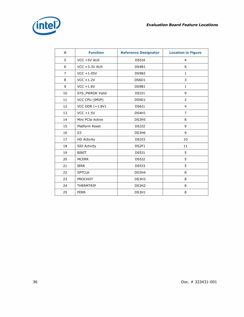
Evaluation Board Feature Locations
36 Doc. # 323431-001
# Function Reference Designator Location in Figure
5 VCC +5V AUX DS5J4 4
6 VCC +3.3V AUX DS4B1 6
7 VCC +1.05V DS9B2 1
8 VCC +1.2V DS6D1 3
9 VCC +1.8V DS9B1 1
10 SYS_PWROK Valid DS3J1 9
11 VCC CPU (IMVP) DS9D1 2
12 VCC DDR (+1.8V) DS6J1 4
13 VCC +1.5V DS4H1 7
14 Mini PCIe Active DS3H5 8
15 Platform Reset DS3J2 9
16 S3 DS3H6 9
17 HD Activity DS3J3 10
18 SIO Activity DS2F1 11
19 BINIT DS5J1 5
20 MCERR DS5J2 5
21 IERR DS5J3 5
22 SPTCLK DS3H4 8
23 PROCHOT DS3H3 8
24 THERMTRIP DS3H2 8
25 FERR DS3H1 8

Evaluation Board Feature Locations
Doc. # 323431-001 37
Figure 7. Board LEDs

Evaluation Board Feature Locations
38 Doc. # 323431-001
5.7 Headers
Figure 8. Board Headers
5.7.1 SPI Programming Headers
The microcontroller firmware for system management/keyboard/mouse control can be upgraded in two ways:
By use of a special MS-DOS utility (in-circuit). See Section 6.3.
By use of an external computer connected (remotely) to the system through the SPI Program header on the board (J5D1). See Table 9 for (J4D1) and (J4C1) jumper settings. See http://dediprog.com/ for programming hardware and software.
5.7.2 ATX Switch/LED Front Panel Header
A 9-pin front panel header (J4J4) is provided for powering up the platform, resetting the platform, and showing disk activity via the front panel of a chassis. Table 11 below describes each pin.

Evaluation Board Feature Locations
Doc. # 323431-001 39
Table 11. ATX Switch/LED Front Panel Header
Pins Description
1/3 Disk Activity LED
2/4 N/A
5/7 Reset Switch
6/8 Power Switch
9 RSVD (+4.95V)
5.7.3 USB Front Panel Header
Two standard 9-pin front panel USB headers (J1D1, J1E4) are provided for external USB 2.0 ports. Table below describes pin functions.
Table 12. USB Front Panel Header
Pins Description
1,2 Front Panel USB Power
3 USB P0 (-)
4 USB P1 (-)
5 USB P0 (+)
6 USB P1 (+)
7,8 Ground
10 USB Overcurrent
5.7.4 TPM Header
A 20-pin header (J1A1) is provided for testing an external TPM. Table 13 details the pin assignments.
Table 13. TPM Header
Pins Description
1 L_CLK
2 Ground
3 L_FRAME#
5 L_RESET#
6 +5V
1
2
1
2

Evaluation Board Feature Locations
40 Doc. # 323431-001
7 L_AD[3]
8 L_AD[2]
9 +3V
10 L_AD[1]
11 L_AD[0]
12 Ground
13 SMB_CLK
14 SMB_DAT
15 +3V Standby
16 SERIRQ
17 Ground
18 CLKRUN#
19 LPCPD#
20 L_DRQ0#
§

Quick Start
Doc. # 323431-001 41
6 Quick Start
The following sections summarize the necessary hardware and power-on instructions for the Intel® Atom™ Processor N450, D410 and D510 with the Intel® 82801HM I/O Controller Hub Development Kit.
Caution: Always turn off the power and unplug the power cord before entering protective chassis.
The user is required to observe extra precautions when handling and operating the
system.
6.1 Required Peripherals DDR2 667-MHz SDRAM SODIMM (Two 1 GB SODIMMS included with development
kit)
ATX power supply (Included with development kit)
SATA hard drive (Included with development kit)
SATA hard drive cable (Optional- Included with development kit)
Mott Canyon with HD Audio (Optional- Included with development kit)
SATA Optical Drive (Optional- Included with development kit)
AC Power cord (Included with development kit)
Keyboard and mouse (not included)
External display (not included)
Note: SATA hard drive cable is optional as the board has a SATA direct connect connector on the board (J2K1).
6.2 Power Up /Power Down
Complete the steps outlined in this section to power up and power down the development board.
6.2.1 Pre-Power Up
Note: Steps 1-7 may already be completed in the development kit. Steps 8-11 will need to be done by the development kit user and board user alike.
1. Place a DDR2 SO-DIMM in memory socket J3V2 (bottom of board) if not populated.
2. Install or verify the configuration jumpers as described in Section 5.4.1.
3. Verify presence of RTC battery in battery holder at B5G1.

Quick Start
42 Doc. # 323431-001
4. Plug in an ATX power supply 24-pin connector into connector J9K1; the connectors are keyed and will only fit in one position. Make sure all 24-pins are used.
5. Connect a SATA hard drive directly to connector J2K1. This connector contains power and data and does not require the use of a SATA hard drive cable.
Note: If internal graphics are not used, plug a PCI Express* Graphics card in the PCI-E x1 Slot 4 (J4B3) and connect a monitor to the card. Only select graphics cards support x1. Steps 6 and 7 are optional; however they have been completed for the development kit.
6. Optional: Attach the Mott Canyon 4 MDC to the MDC header at J1B3 and J1C1. An Intel® HD Audio card can be piggybacked onto the Mott Canyon 4 card to provide soft audio and soft modem functionality. Adapter cables, speakers, or a phone line for a modem may be needed, depending on the specific card used.
7. Optional: Attach a desktop CD-ROM (or mobile CD-ROM with adapter) with PATA cable to connector J4K2 (red stripe toward pin 1), or with SATA cable to J1G1 or J1H1. Attach power to an ATX power supply. If two IDE devices are used on the same PATA channel, one must be set to master and one must be set to slave. Check the operating instructions for the IDE devices.
Note: Steps 8-11 should be completed by development kit user‘s as well as board users.
8. Connect a USB keyboard to the front or back Panel of Chassis (see Appendix E) or Connector J5A1 on board.
9. Connect a USB mouse to the front or back Panel of Chassis (see Appendix E) or Connector J5A1 on board.
10. Connect VGA monitor to back panel of Chassis, connector J8A1 (see Section 5.3.1)
11. Plug in the AC plug from the ATX power supply (see Appendix E) to an AC outlet.
6.2.2 Powering Up the Board
1. Press the power button on the front of the chassis (see Appendix E) or button located at S4J1 on board.
2. As the system boots (During POST test), press either the F2 key or the Del key on the keyboard to enter the Firmware setup screen.
3. Check time, date, and configuration settings. For most users the default settings should be sufficient for the initial bring-up.
4. Press the F4 key to save and exit the firmware setup.
5. The system reboots and is ready for use.
Note: If the board does not power up completely, the Port 80 code on the 7-segment displays (DS1J1 and DS1K1) may provide insight into the issue. See AMI‘s Aptio* site for details of these status codes - http://www.ami.com/aptio/
Quick Start
Doc. # 323431-001 43
6.2.3 Powering Down the Board
There are three options for powering-down the board:
Use OS-controlled shutdown through the Windows Start menu (or equivalent)
Press the power button on the Chassis or the motherboard at S4J1 to begin power-down.
If the system is hung, it is possible to asynchronously shut the system down by holding the power button down continuously for 4 seconds.
Note: Intel does not recommend powering down the board by shutting off power at the ATX power supply.
6.3 Firmware Updates
To update the EFI image in DOS to a newer release, use the EFI binary image and a BIOS update utility. One utility that can be used is the AFUDOS BIOS update utility, also referred to as a ―BIOS flash utility‖, with a command line interface for MS-DOS. This utility is available through AMI and can be accessed here.
Getting Started:
Copy the AFUDOS.EXE executable file to any storage location accessible by the host system and then run AFUDOS in a DOS environment command prompt.
Basic Usage:
AFUDOS CMCKXXXX.ROM /P /C (XXXX is the BIOS version to be flashed)
Program main BIOS image, reset CMOS to defaults
AFUDOS ROMFILE.ROM /P /B /N /C
Program main BIOS image & bootblock image
Reset CMOS and NVRAM to defaults
EFI firmware updates can be found on the Intel® Validation Internet Portal (VIP) – https://platformsw.intel.com.
Note: Afudos.exe comes in two versions, one for legacy BIOS update and one for EFI BIOS update. These two versions are not cross compatible. Using afudos.exe for legacy BIOS to update an EFI BIOS will generate an error message such as memory error. Please make sure to download the latest afudos.exe for EFI BIOS to update the evaluation board. AMI‘s EFI BIOS is called AMI Aptio.
§
Quick Start
44 Doc. # 323431-001
Appendix A Daughter and Plug-In
Cards
A.1 Mott Canyon 4 Interposer Card
The Mott Canyon 4 Interposer card is provided to enable Intel® HD Audio functionality on the Board. Functionality includes:
Supports three Mobile Daughter Card (MDC) headers and up to two Intel® High Definition codecs simultaneously
Plugs into a PCI Express* slot—for mechanical stability only
Electrically connected to the platform through a 26-pin ribbon cable from the Mott Canyon 4 Interposer card to a 2 x 8 header (J1B3) and 2 x 4 header (J1C1) on The evaluation board
Intel® HD Audio MDC cards may require sideband signal cables for proper operation
Headers on the Mott Canyon 4 card are provided for both modem and audio sideband signals
For additional information, see Sheet 54 of the board schematics.

Quick Start
Doc. # 323431-001 45
Figure 9. Mott Canyon 4 Interposer Card
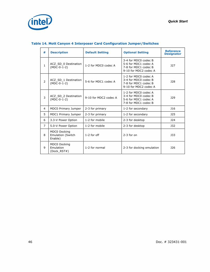
A.1.1 Jumper Settings
The Mott Canyon 4 Interposer card can select either Primary or Secondary Intel® HD Audio functionality for MDC0 and MDC1 connectors with two jumper options, J16 and J25.
In Intel® HD Audio mode, MDC0 is designed to house the primary codec (usually audio but could be modem if there is no audio) and if necessary, MDC1 is designed to house the modem codec. MDC2 supports an Intel® HD Audio modem-only codec.
Intel® 82801HM I/O Controller supports up to two SDATA_IN channels (0, 1). Two jumpers, J27 and J28 are used to select the appropriate SDATA_IN channels for each of the MDCs. Be aware that SDATA_IN channels 1 and 2 can be also overridden through jumpers on the evaluation platform. If either SDATA_IN1 or SDATA_IN2 are not shunted properly on the evaluation platform, these lines are not available to the Mott Canyon 4 Interposer card. Proper operation of the Intel® HD Audio interface requires that only one SDATA_IN line is routed to one codec at a time.
Table 14 summarizes the default and optional settings for the jumper/switches.
Quick Start
46 Doc. # 323431-001
Table 14. Mott Canyon 4 Interposer Card Configuration Jumper/Switches
# Description Default Setting Optional Setting Reference Designator
1 ACZ_SD_0 Destination
(MDC-0-1-2) 1-2 for MDC0 codec A
3-4 for MDC0 codec B
5-6 for MDC1 codec A
7-8 for MDC1 codec B
9-10 for MDC2 codec A
J27
2 ACZ_SD_1 Destination
(MDC-0-1-2) 5-6 for MDC1 codec A
1-2 for MDC0 codec A
3-4 for MDC0 codec B
7-8 for MDC1 codec B
9-10 for MDC2 codec A
J28
3 ACZ_SD_2 Destination
(MDC-0-1-2) 9-10 for MDC2 codec A
1-2 for MDC0 codec A
3-4 for MDC0 codec B
5-6 for MDC1 codec A
7-8 for MDC1 codec B
J29
4 MDC0 Primary Jumper 2-3 for primary 1-2 for secondary J16
5 MDC1 Primary Jumper 2-3 for primary 1-2 for secondary J25
6 3.3-V Power Option 1-2 for mobile 2-3 for desktop J24
7 5.0-V Power Option 1-2 for mobile 2-3 for desktop J32
8
MDC0 Docking
Emulation (Switch
Enable)
1-2 for off 2-3 for on J33
9
MDC0 Docking
Emulation
(Dock_RST#)
1-2 for normal 2-3 for docking emulation J26
Quick Start
Doc. # 323431-001 47
A.1.2 Audio Firmware Configuration
To enable High Definition Audio functionality, the firmware settings may need to be modified.
To modify the firmware settings:
1. With the system powered off, press the power button located at S4J1.
2. As the system boots, press either the F2 key or the Del key on the keyboard to enter the Firmware setup screen.
3. Move the top cursor (using the sideways arrow keys) to Chipset.
4. Move the screen cursor (using the up/down arrow keys) to South Bridge Configuration and press the Enter key.
5. Move the screen cursor (using the up/down arrow keys) to ICH8-M Devices and press the enter key.
6. Move the screen cursor to Audio Controller and press the Enter key.
7. Select Azalia for the audio codec.
8. Save the settings and exit the Firmware (F4 key).
§

Quick Start
48 Doc. # 323431-001
Appendix B Intel® MVP-6 VID Codes
Table 15. Voltage Identification Definition
VID6 VID5 VID4 VID3 VID2 VID1 VID0 VCC (V)
0 0 1 1 0 0 0 1.2000
0 0 1 1 0 0 1 1.1875
0 0 1 1 0 1 0 1.1750
0 0 1 1 0 1 1 1.1625
0 0 1 1 1 0 0 1.1500
0 0 1 1 1 0 1 1.1375
0 0 1 1 1 1 0 1.1250
0 0 1 1 1 1 1 1.1125
0 1 0 0 0 0 0 1.1000
0 1 0 0 0 0 1 1.0875
0 1 0 0 0 1 0 1.0750
0 1 0 0 0 1 1 1.0625
0 1 0 0 1 0 0 1.0500
0 1 0 0 1 0 1 1.0375
0 1 0 0 1 1 0 1.0250
0 1 0 0 1 1 1 1.0125
0 1 0 1 0 0 0 1.0000
0 1 0 1 0 0 1 0.9875
0 1 0 1 0 1 0 0.9750
0 1 0 1 0 1 1 0.9625
0 1 0 1 1 0 0 0.9500
0 1 0 1 1 0 1 0.9375
0 1 0 1 1 1 0 0.9250
0 1 0 1 1 1 1 0.9125
Quick Start
Doc. # 323431-001 49
VID6 VID5 VID4 VID3 VID2 VID1 VID0 VCC (V)
0 1 1 0 0 0 0 0.9000
0 1 1 0 0 0 1 0.8875
0 1 1 0 0 1 0 0.8750
0 1 1 0 0 1 1 0.8625
0 1 1 0 1 0 0 0.8500
0 1 1 0 1 0 1 0.8375
0 1 1 0 1 1 0 0.8250
0 1 1 0 1 1 1 0.8125
0 1 1 1 0 0 0 0.8000
0 1 1 1 0 0 1 0.7875
0 1 1 1 0 1 0 0.7750
0 1 1 1 0 1 1 0.7625
0 1 1 1 1 0 0 0.7500
0 1 1 1 1 0 1 0.7375
0 1 1 1 1 1 0 0.7250
0 1 1 1 1 1 1 0.7125
1 0 0 0 0 0 0 0.7000
1 0 0 0 0 0 1 0.6875
1 0 0 0 0 1 0 0.6750
1 0 0 0 0 1 1 0.6625
1 0 0 0 1 0 0 0.6500
1 0 0 0 1 0 1 0.6375
1 0 0 0 1 1 0 0.6250
1 0 0 0 1 1 1 0.6125
1 0 0 1 0 0 0 0.6000
1 0 0 1 0 0 1 0.5875
1 0 0 1 0 1 0 0.5750
1 0 0 1 0 1 1 0.5625
1 0 0 1 1 0 0 0.5500
Quick Start
50 Doc. # 323431-001
VID6 VID5 VID4 VID3 VID2 VID1 VID0 VCC (V)
1 0 0 1 1 0 1 0.5375
1 0 0 1 1 1 0 0.5250
1 0 0 1 1 1 1 0.5125
1 0 1 0 0 0 0 0.5000
1 0 1 0 0 0 1 0.4875
1 0 1 0 0 1 0 0.4750
1 0 1 0 0 1 1 0.4625
1 0 1 0 1 0 0 0.4500
1 0 1 0 1 0 1 0.4375
1 0 1 0 1 1 0 0.4250
1 0 1 0 1 1 1 0.4125
1 0 1 1 0 0 0 0.4000
1 0 1 1 0 0 1 0.3875
1 0 1 1 0 1 0 0.3750
1 0 1 1 0 1 1 0.3625
1 0 1 1 1 0 0 0.3500
1 0 1 1 1 0 1 0.3375
1 0 1 1 1 1 0 0.3250
1 0 1 1 1 1 1 0.3125
1 1 0 0 0 0 0 0.3000
§
Quick Start
Doc. # 323431-001 51
Appendix C VRD11 VID Codes
Table 16. Voltage Identification Definition
VID6 VID5 VID4 VID3 VID2 VID1 VID0 VCC (V)
0 1 0 0 0 0 1 1.2
0 1 0 0 0 1 0 1.1875
0 1 0 0 0 1 1 1.175
0 1 0 0 1 0 0 1.1625
0 1 0 0 1 0 1 1.15
0 1 0 0 1 1 0 1.1375
0 1 0 0 1 1 1 1.125
0 1 0 1 0 0 0 1.1125
0 1 0 1 0 0 1 1.1
0 1 0 1 0 1 0 1.0875
0 1 0 1 0 1 1 1.075
0 1 0 1 1 0 0 1.0625
0 1 0 1 1 0 1 1.05
0 1 0 1 1 1 0 1.0375
0 1 0 1 1 1 1 1.025
0 1 1 0 0 0 0 1.0125
0 1 1 0 0 0 1 1

Quick Start
52 Doc. # 323431-001
VID6 VID5 VID4 VID3 VID2 VID1 VID0 VCC (V)
0 1 1 0 0 1 0 0.9875
0 1 1 0 0 1 1 0.975
0 1 1 0 1 0 0 0.9625
0 1 1 0 1 0 1 0.95
0 1 1 0 1 1 0 0.9375
0 1 1 0 1 1 1 0.925
0 1 1 1 0 0 0 0.9125
0 1 1 1 0 0 1 0.9
0 1 1 1 0 1 0 0.8875
0 1 1 1 0 1 1 0.875
0 1 1 1 1 0 0 0.8625
0 1 1 1 1 0 1 0.85
0 1 1 1 1 1 0 0.8375
0 1 1 1 1 1 1 0.825
1 0 0 0 0 0 0 0.8125
1 0 0 0 0 0 1 0.8
1 0 0 0 0 1 0 0.7875
1 0 0 0 0 1 1 0.775
1 0 0 0 1 0 0 0.7625
1 0 0 0 1 0 1 0.75
Quick Start
Doc. # 323431-001 53
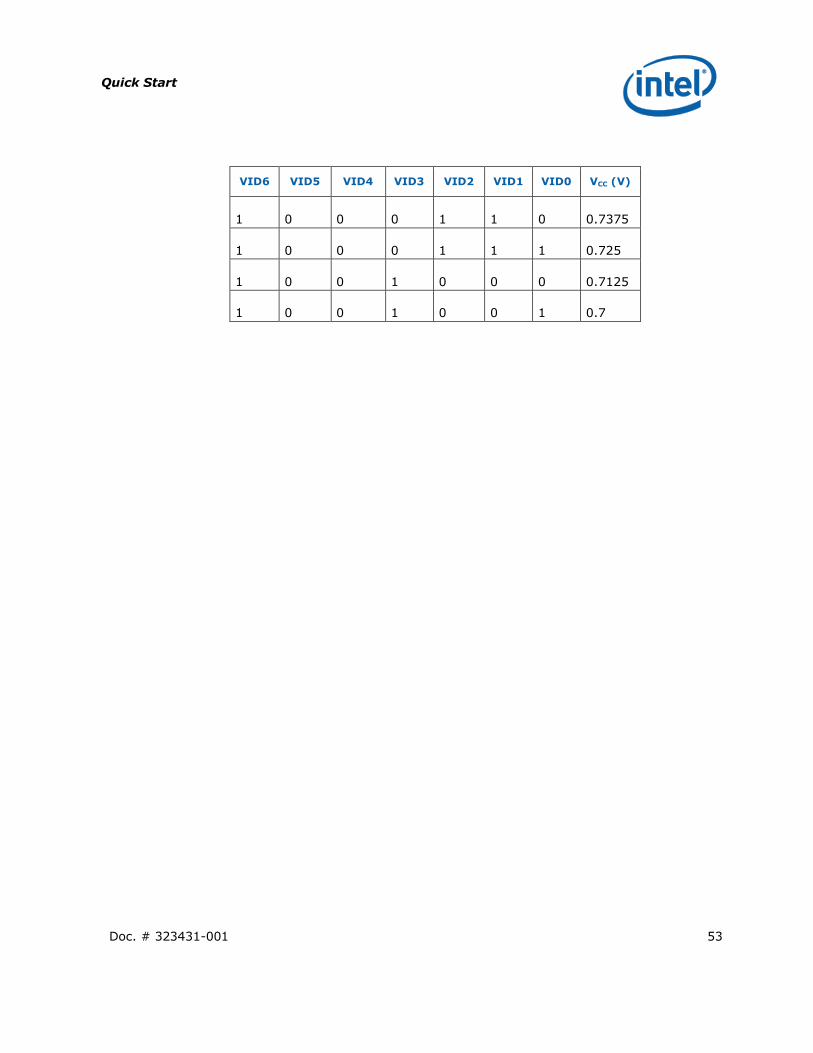
VID6 VID5 VID4 VID3 VID2 VID1 VID0 VCC (V)
1 0 0 0 1 1 0 0.7375
1 0 0 0 1 1 1 0.725
1 0 0 1 0 0 0 0.7125
1 0 0 1 0 0 1 0.7

Quick Start
54 Doc. # 323431-001
Appendix D PCI Express* Ports
D.1 Configuring PCI Express* Ports
Figure 10. PCI Express* Configuration Block Diagram with Default Configuration
Slot 2
Slot 3
Slot 4
Slot 5
USB
82567V
GbE
ICH8M
0 ohm Empty
Resistor Group1
0 ohm Empty
Resistor Group1
EXP_SLOT2 * <2>
0 ohm
Resistor Group2
0 ohm Empty
Resistor Group4
0 ohm
Resistor Group3
EXP_SLOT 3*<0>
EXP_SLOT 3*<1>
EXP_SLOT 2*<3>
PCIe[3] x1
PCIe[4] x1
PCIe[1-2] x2
EXP_SLOT 4*<0>
8.2k
empty
VCC3P3_PS
8.2k
HDA_SDOUT
HDA_SYNC
GLCI/PCIe[6]
PCIe[5] x1
Flexibility has been designed into the implementation of the PCI Express* slots on the board. While the Intel® 82801HM I/O Controller supports six x1 links, there are only three conventional PCIe slots and one Mini PCIe slot as shown above. By default, each slot is capable of at least x1 operation. Slot 2 is also capable of x2 (not a standard PCIe width - for custom PCIe implementations) by default. But there are two more configurations possible: one that disables Slot 4 and allows x2 operation on Slot 3 in addition to Slot 2, another that disables Slot 4 and Slot 3, and allows x4 operation on Slot 2. See Figure 4 for physical slot locations.
Note: Use this section in conjunction with the board schematics and silk screen.

Quick Start
Doc. # 323431-001 55
Table 17. PCIe Slot Configurations
Configuration Slot 2 Slot 3 Slot 4
1 x4
2 x2 x1 x1
3 x2 x2
Note: Configuration 2 is the shipping default.
Slot flexibility is achieved by routing some PCIe lanes from the ICH to more than one slot. Of course one lane can‘t be used by two slots at the same time, so resistors are used to populate one route or another.
In order to simplify the configurations conceptually, each route‘s resistors are specified as a group. Table 18 shows these groups and specifies the default groups that are populated or not (empty) to implement Configuration 2. Below is a table linking groups to configurations.
Table 18. PCIe Route Groups
Configuration Group 1 Group 2 Group 3 Group 4
1 Populated Empty Empty Empty
2 Empty Populated Populated Empty
3 Empty Populated Empty Populated
Next is the list of resistors for each group.
Table 19. PCIe Group Resistors
ICH Lane Group 1 Group 2 Group 3 Group 4
2 TX + R8N3 R8N2
2 TX - R8N5 R8N4
2 RX + R8N7 R8N6
2 RX - R8N9 R8N8
3 TX + R7P3 R7P1 R7P2
3 TX - R7P5 R7P4 R7P6
3 RX + R7P7 R7P8 R7P9
3 RX - R7P11 R7P12 R7P10
And finally, a full table specifying which resistors to populate or de-populate depending on configuration option desired.
Quick Start
56 Doc. # 323431-001
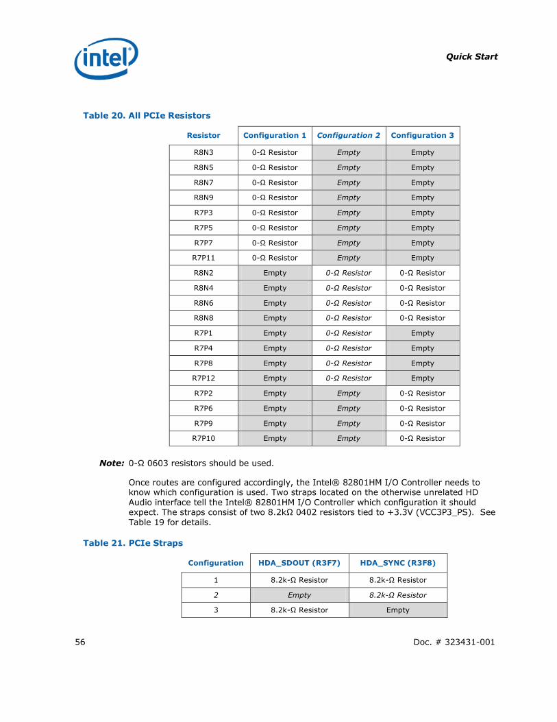
Table 20. All PCIe Resistors
Resistor Configuration 1 Configuration 2 Configuration 3
R8N3 0-Ω Resistor Empty Empty
R8N5 0-Ω Resistor Empty Empty
R8N7 0-Ω Resistor Empty Empty
R8N9 0-Ω Resistor Empty Empty
R7P3 0-Ω Resistor Empty Empty
R7P5 0-Ω Resistor Empty Empty
R7P7 0-Ω Resistor Empty Empty
R7P11 0-Ω Resistor Empty Empty
R8N2 Empty 0-Ω Resistor 0-Ω Resistor
R8N4 Empty 0-Ω Resistor 0-Ω Resistor
R8N6 Empty 0-Ω Resistor 0-Ω Resistor
R8N8 Empty 0-Ω Resistor 0-Ω Resistor
R7P1 Empty 0-Ω Resistor Empty
R7P4 Empty 0-Ω Resistor Empty
R7P8 Empty 0-Ω Resistor Empty
R7P12 Empty 0-Ω Resistor Empty
R7P2 Empty Empty 0-Ω Resistor
R7P6 Empty Empty 0-Ω Resistor
R7P9 Empty Empty 0-Ω Resistor
R7P10 Empty Empty 0-Ω Resistor
Note: 0-Ω 0603 resistors should be used.
Once routes are configured accordingly, the Intel® 82801HM I/O Controller needs to know which configuration is used. Two straps located on the otherwise unrelated HD Audio interface tell the Intel® 82801HM I/O Controller which configuration it should expect. The straps consist of two 8.2kΩ 0402 resistors tied to +3.3V (VCC3P3_PS). See Table 19 for details.
Table 21. PCIe Straps
Configuration HDA_SDOUT (R3F7) HDA_SYNC (R3F8)
1 8.2k-Ω Resistor 8.2k-Ω Resistor
2 Empty 8.2k-Ω Resistor
3 8.2k-Ω Resistor Empty

Quick Start
Doc. # 323431-001 57
See the Intel® Atom™ N450, D410 and D510 Embedded Platform Technical Update for the Intel® 82801HM I/O Controller - Enabling Additional PCIe Port Configurations for details of this last strapping. Contact your Intel Representative for access to this document.
§

Quick Start
58 Doc. # 323431-001
Appendix E Development Kit Chassis
Features
E.1 External Feature Locations
This section describes the features and use of the chassis and components provided with the development kit. This chassis and its modifications directly support the Intel® Atom™ Processor N450, D410 and D510 with the Intel® 82801HM I/O Controller board.

Quick Start
Doc. # 323431-001 59
E.1.1 Front of Chassis
The Front of the chassis offers a power button, reset button, disk activity LED, four USB access ports, and access to the CD/DVD ROM.
Note: The 1394 and Audio ‘97 connectors on the chassis are not connected to the board and hence the Front Panel Audio Jacks as well as the IEEE 1397 connectors are non functional.
Figure 11. Front of Chassis
Quick Start
60 Doc. # 323431-001
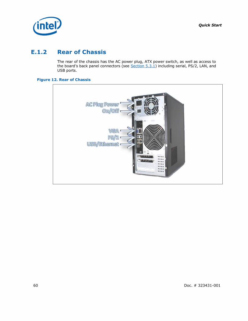
E.1.2 Rear of Chassis
The rear of the chassis has the AC power plug, ATX power switch, as well as access to the board‘s back panel connectors (see Section 5.3.1) including serial, PS/2, LAN, and USB ports.
Figure 12. Rear of Chassis

Quick Start
Doc. # 323431-001 61
E.2 Internal Components
All included hardware is located inside the development kit Chassis. The board is connected to a removable plate. The ATX power supply sits in the rear ATX power supply cradle, while the hard drive and CD/DVD ROM sit in the cradles across from it. Both hard drive and DVD/ROM are connected to the board with SATA cables. The Mott Canyon 4 card with Azalia* HD Audio is connected and installed in PCI slots 3 & 4. There are also cables connecting the front panel buttons and connectors to the board.
Note: The Mott Canyon 4 Card is only inserted into the PCIe slots 3&4 for support. It does not have an electrical connection to the PCIe slots.
Figure 13. Internal Components of Development Kit
E.3 Accessing the Board
The chassis has a unique feature that allows the motherboard to be removed from the chassis while maintaining most connections and operability. Please follow the steps below.
Remove the black chassis side panels. This can be done by unscrewing the screws along the edge of the on the back side of the chassis and then sliding off each panel.
Unscrew, un-connect, and remove any and all PCIe cards.

Quick Start
62 Doc. # 323431-001
The motherboard is connected to a tray. This tray is removable once the tray screw has been removed. The tray screw is located on the back of the chassis beside the I/O panel. Unscrew this screw.
Figure 14. Motherboard Tray Removal
Once the tray screw has been removed, slide the tray towards the front of the chassis and then pull it out away from the chassis.
Quick Start
Doc. # 323431-001 63
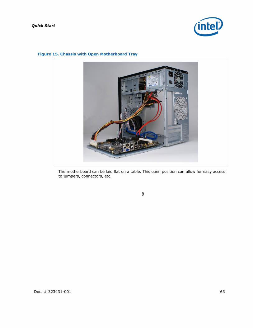
Figure 15. Chassis with Open Motherboard Tray
The motherboard can be laid flat on a table. This open position can allow for easy access to jumpers, connectors, etc.
§