Embed Size (px)
Citation preview
Atom-by-Atom Observation of Grain Boundary Migration inGrapheneSimon Kurasch,†,¶ Jani Kotakoski,*,‡,§,¶,● Ossi Lehtinen,‡,¶,● Viera Skakalova,∥,■ Jurgen Smet,∥
Carl E. Krill, III,⊥ Arkady V. Krasheninnikov,‡,# and Ute Kaiser*,†
†Central Facility for Electron Microscopy, Group of Electron Microscopy of Materials Science, Ulm University, 89081 Ulm, Germany‡Department of Physics, University of Helsinki, P.O. Box 43, 00014 Helsinki, Finland§Department of Physics, University of Vienna, Boltzmanngasse 5, 1090 Vienna, Austria∥Max Planck Institute for Solid State Research, Heisenbergstrasse 1, 70569 Stuttgart, Germany⊥Institute of Micro and Nanomaterials, Ulm University, Albert-Einstein-Allee 47, 89081 Ulm, Germany#Department of Applied Physics, Aalto University, P.O. Box 1100, 00076 Aalto, Finland
*S Supporting Information
ABSTRACT: Grain boundary (GB) migration in polycrystalline solids is a materials science manifestation of survival of thefittest, with adjacent grains competing to add atoms to their outer surfaces at each other’s expense. This process isthermodynamically favored when it lowers the total GB area in the sample, thereby reducing the excess free energy contributedby the boundaries. In this picture, a curved boundary is expected to migrate toward its center of curvature with a velocityproportional to the local radius of boundary curvature (R). Investigating the underlying mechanism of boundary migration in a3D material, however, has been reserved for computer simulation or analytical theory, as capturing the dynamics of individualatoms in the core region of a GB is well beyond the spatial and temporal resolution limits of current characterization techniques.Here, we similarly overcome the conventional experimental limits by investigating a 2D material, polycrystalline graphene, in anaberration-corrected transmission electron microscope, exploiting the energy of the imaging electrons to stimulate individualbond rotations in the GB core region. The resulting morphological changes are followed in situ, atom-by-atom, revealingconfigurational fluctuations that take on a time-averaged preferential direction only in the presence of significant boundarycurvature, as confirmed by Monte Carlo simulations. Remarkably, in the extreme case of a small graphene grain enclosed within alarger one, we follow its shrinkage to the point of complete disappearance.
KEYWORDS: Graphene, transmission electron microscopy, grain boundaries, Monte Carlo, transformation, migration
Adjacent grains in polycrystalline graphene are separated bytilt boundaries. The low-energy configurations of these
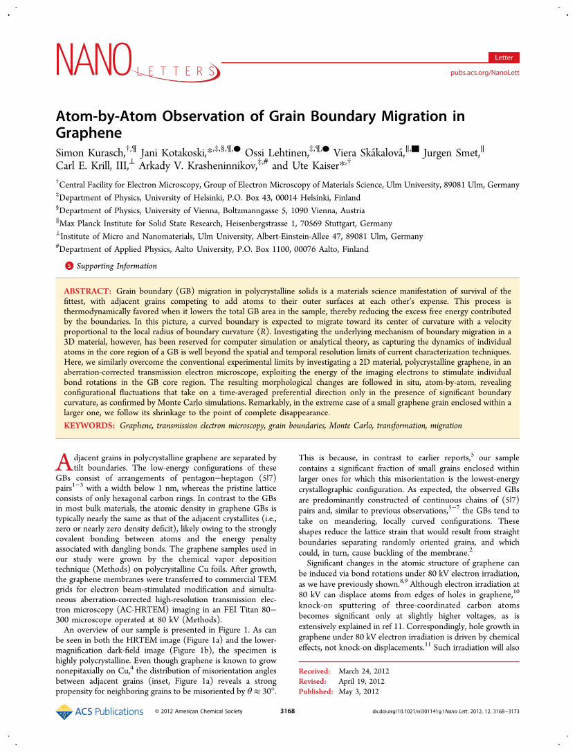
GBs consist of arrangements of pentagon−heptagon (5|7)pairs1−3 with a width below 1 nm, whereas the pristine latticeconsists of only hexagonal carbon rings. In contrast to the GBsin most bulk materials, the atomic density in graphene GBs istypically nearly the same as that of the adjacent crystallites (i.e.,zero or nearly zero density deficit), likely owing to the stronglycovalent bonding between atoms and the energy penaltyassociated with dangling bonds. The graphene samples used inour study were grown by the chemical vapor depositiontechnique (Methods) on polycrystalline Cu foils. After growth,the graphene membranes were transferred to commercial TEMgrids for electron beam-stimulated modification and simulta-neous aberration-corrected high-resolution transmission elec-tron microscopy (AC-HRTEM) imaging in an FEI Titan 80−300 microscope operated at 80 kV (Methods).An overview of our sample is presented in Figure 1. As can
be seen in both the HRTEM image (Figure 1a) and the lower-magnification dark-field image (Figure 1b), the specimen ishighly polycrystalline. Even though graphene is known to grownonepitaxially on Cu,4 the distribution of misorientation anglesbetween adjacent grains (inset, Figure 1a) reveals a strongpropensity for neighboring grains to be misoriented by θ ≈ 30°.
This is because, in contrast to earlier reports,5 our samplecontains a significant fraction of small grains enclosed withinlarger ones for which this misorientation is the lowest-energycrystallographic configuration. As expected, the observed GBsare predominantly constructed of continuous chains of (5|7)pairs and, similar to previous observations,5−7 the GBs tend totake on meandering, locally curved configurations. Theseshapes reduce the lattice strain that would result from straightboundaries separating randomly oriented grains, and whichcould, in turn, cause buckling of the membrane.2
Significant changes in the atomic structure of graphene canbe induced via bond rotations under 80 kV electron irradiation,as we have previously shown.8,9 Although electron irradiation at80 kV can displace atoms from edges of holes in graphene,10
knock-on sputtering of three-coordinated carbon atomsbecomes significant only at slightly higher voltages, as isextensively explained in ref 11. Correspondingly, hole growth ingraphene under 80 kV electron irradiation is driven by chemicaleffects, not knock-on displacements.11 Such irradiation will also
Received: March 24, 2012Revised: April 19, 2012Published: May 3, 2012
Letter
pubs.acs.org/NanoLett
© 2012 American Chemical Society 3168 dx.doi.org/10.1021/nl301141g | Nano Lett. 2012, 12, 3168−3173
cause only slight heating of the sample.12 At voltages below 80kV, bond rotations are too scarce to lead to significantconfigurational changes5 (the lower the voltage, the fewer bondrotations per unit time). Therefore, by exposing graphene to 80keV electrons, we deliberately maximize the bond rotation rate,resulting in measurable changes in graphene GB morphologyduring the time scale of a typical experiment in the electronmicroscope. In the case of straight twin boundaries, the GBenergy per unit length (γ) has already been shown to dependprimarily on the misorientation angle θ.1−3 According to ourdensity functional theory (DFT) calculations (Methods), thisremains true also for more realistic, serpentine GB config-urations (for θ ≈ 30° all γ are within 0.03 eV/Å, the absolutevalue being an order of magnitude higher). Therefore, thedriving force (per unit GB length) for migration of a given GBbetween two grains, γ/R,13 should depend only on its local in-plane curvature and not on its detailed atomic structure. Hence,at low boundary curvature (R → ∞) there is no preferreddirection of migration, whereas in the high-curvature limit (R→ 0) the driving force should favor decreasing the GB lengthand thereby shrinking the grain located on the same side of theboundary as the center of curvature. The decrease of GB lengthin a 2D material is analogous to decrease of GB area inconventional 3D materials.We first consider the behavior of boundaries between larger
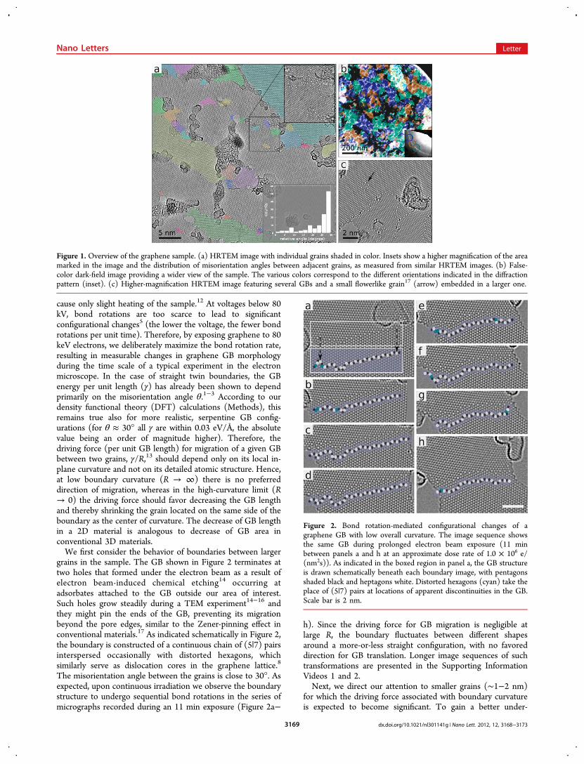
grains in the sample. The GB shown in Figure 2 terminates attwo holes that formed under the electron beam as a result ofelectron beam-induced chemical etching14 occurring atadsorbates attached to the GB outside our area of interest.Such holes grow steadily during a TEM experiment14−16 andthey might pin the ends of the GB, preventing its migrationbeyond the pore edges, similar to the Zener-pinning effect inconventional materials.17 As indicated schematically in Figure 2,the boundary is constructed of a continuous chain of (5|7) pairsinterspersed occasionally with distorted hexagons, whichsimilarly serve as dislocation cores in the graphene lattice.8
The misorientation angle between the grains is close to 30°. Asexpected, upon continuous irradiation we observe the boundarystructure to undergo sequential bond rotations in the series ofmicrographs recorded during an 11 min exposure (Figure 2a−
h). Since the driving force for GB migration is negligible atlarge R, the boundary fluctuates between different shapesaround a more-or-less straight configuration, with no favoreddirection for GB translation. Longer image sequences of suchtransformations are presented in the Supporting InformationVideos 1 and 2.Next, we direct our attention to smaller grains (∼1−2 nm)
for which the driving force associated with boundary curvatureis expected to become significant. To gain a better under-
Figure 1. Overview of the graphene sample. (a) HRTEM image with individual grains shaded in color. Insets show a higher magnification of the areamarked in the image and the distribution of misorientation angles between adjacent grains, as measured from similar HRTEM images. (b) False-color dark-field image providing a wider view of the sample. The various colors correspond to the different orientations indicated in the diffractionpattern (inset). (c) Higher-magnification HRTEM image featuring several GBs and a small flowerlike grain17 (arrow) embedded in a larger one.
Figure 2. Bond rotation-mediated configurational changes of agraphene GB with low overall curvature. The image sequence showsthe same GB during prolonged electron beam exposure (11 minbetween panels a and h at an approximate dose rate of 1.0 × 10⁶ e/(nm2s)). As indicated in the boxed region in panel a, the GB structureis drawn schematically beneath each boundary image, with pentagonsshaded black and heptagons white. Distorted hexagons (cyan) take theplace of (5|7) pairs at locations of apparent discontinuities in the GB.Scale bar is 2 nm.
Nano Letters Letter
dx.doi.org/10.1021/nl301141g | Nano Lett. 2012, 12, 3168−31733169
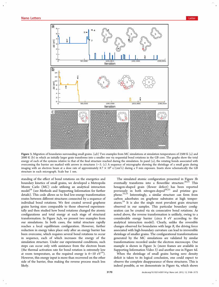
standing of the effect of bond rotations on the energetics andboundary kinetics of small grains, we developed a MetropolisMonte Carlo (MC) code utilizing an analytical interactionmodel18 (see Methods and Supporting Information for furtherdetails). This code allows us to find low-energy transformationroutes between different structures connected by a sequence ofindividual bond rotations. We first created several graphenegrains having sizes comparable to those observed experimen-tally and then studied how bond rotations changed the atomicconfigurations and total energy at each stage of structuraltransformation. In Figure 3a,b, we present two examples fromour simulations. In both cases, the initial structure rapidlyreaches a local equilibrium configuration. However, furtherreduction in energy takes place only after an energy barrier hasbeen overcome, which requires several bond rotations to occurin sequence, each of which increases the energy of thesimulation structure. Under our experimental conditions, suchsteps can occur only with assistance from the electron beam(the thermal activation rate for bond rotation is extremely lowat room temperature, as the required energy is 6−10 eV19).However, this energy input is more than recovered on the otherside of the barrier, thus making the reverse process much lesslikely.
The simulated atomic configuration presented in Figure 3beventually transforms into a flowerlike structure.20,21 Thishexagon-shaped grain (flower defect) has been reportedpreviously in both nitrogen-doped20,21 and pristine gra-phene.22,23 Interestingly, a similar structure can form fromcarbon adsorbates on graphene substrates at high temper-atures.24 It is also the single most prevalent grain structureobserved in our samples. This particular boundary config-uration can be created via six consecutive bond rotations. Asnoted above, the reverse transformation is unlikely, owing to aconsiderable energy barrier (circa 8 eV according to theanalytical interaction model). Clearly, unlike the reversiblechanges observed for boundaries with large R, the driving forceassociated with high-boundary curvature can lead to irreversibleshrinkage of smaller grains. The configurational transformationsgenerated by the MC simulations are validated by similartransformations recorded under the electron microscope. Oneexample is shown in Figure 3c (more frames are available inSupporting Information Video 3) and another one in Figure 4d.When the shrinkage of small grains having zero density
deficit is taken to its logical conclusion, one could expect toobserve the complete disappearance of these structures. This isindeed possible, as we demonstrate in Figure 4a, which shows
Figure 3.Migration of boundaries surrounding small grains. (a,b) Two examples from MC simulations at simulation temperatures of 2500 K (a) and2000 K (b) in which an initially larger grain transforms into a smaller one via sequential bond rotations in the GB core. The graphs show the totalenergy of each of the systems relative to that of the final structure reached during the simulation. In panel (a), the rotating bonds associated withovercoming the barrier are marked with arrows in structures 1−3. (c) A sequence of micrographs showing the shrinkage of a small grain duringimaging with an electron beam at a dose rate of approximately 8.7 × 10⁶ e/(nm2s) during a 9 min exposure. Insets show schematically the GBstructure in each micrograph. Scale bar 1 nm.
Nano Letters Letter
dx.doi.org/10.1021/nl301141g | Nano Lett. 2012, 12, 3168−31733170
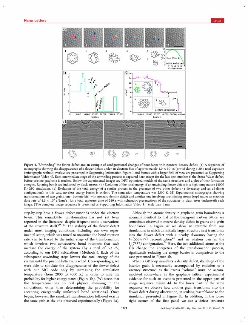
step-by-step how a flower defect unwinds under the electronbeam. This remarkable transformation has not yet beenreported in the literature, despite frequent static observationsof the structure itself.20−23 The stability of the flower defectunder most imaging conditions, including our own exper-imental setup, which was tuned to maximize the bond rotationrate, can be traced to the initial stage of the transformation,which involves two consecutive bond rotations that eachincrease the energy of the system (by a total of ∼3 eV,according to our DFT calculations (Methods)). Each of thesubsequent unwinding steps lowers the total energy of thesystem until the pristine lattice is reached. Correspondingly, wewere able to simulate the disappearance of the flower defectwith our MC code only by increasing the simulationtemperature (from 2000 to 4000 K) in order to raise theprobability for higher-energy states (Figure 4b). (We stress thatthe temperature has no real physical meaning in thesimulations, other than determining the probability foraccepting energetically unfavored bond rotations.) Oncebegun, however, the simulated transformation followed exactlythe same path as the one observed experimentally (Figure 4a).
Although the atomic density in graphene grain boundaries isnormally identical to that of the hexagonal carbon lattice, wesometimes observed nonzero density deficit in grains and grainboundaries. In Figure 4c we show an example from oursimulations in which an initially larger structure first transformsinto the flower defect with a nearby divacancy having theV2(555-777) reconstruction25 and an adatom pair in theI2(7557) configuration.
26 Here, the two additional atoms at theGB change the energetics of the transformation process,significantly reducing the energy barrier in comparison to thecase presented in Figure 4b.When a GB loop manifests a density deficit, shrinkage of the
interior grain is necessarily accompanied by emission of avacancy structure, as the excess “volume” must be accom-modated somewhere in the graphene lattice; experimentalevidence for such an event is presented in the upper part ofimage sequence Figure 4d. In the lower part of the samesequence, we observe how another grain transforms into theflower defect during observation, in striking resemblance to thesimulation presented in Figure 3b. In addition, in the lowerright corner of the first panel we see a defect structure
Figure 4. “Unwinding” the flower defect and an example of configurational changes of boundaries with nonzero density deficit. (a) A sequence ofmicrographs showing the disappearance of a flower defect under an electron flux of approximately 1.0 × 10⁷ e/(nm2s) during a 30 s total exposure(micrographs without overlays are presented in Supporting Information Figure 1 and frames with a larger field of view are presented as SupportingInformation Video 4). Each intermediate stage of the unwinding process is captured here except for the last one, number 6, the Stone-Wales defect,before pristine graphene is reached. Below the experimental images are DFT-optimized models of the same structures and a plot of their formationenergies. Rotating bonds are indicated by black arrows. (b) Evolution of the total energy of an unwinding flower defect in a high-temperature (4000K) MC simulation. (c) Evolution of the total energy of a similar process in the presence of two other defects (a divacancy and an ad-dimerconfiguration); in this case, no clear energy barrier is evident. The simulation temperature was 2500 K. (d) Experimental micrographs showingtransformations of two grains, one (bottom-left) with nonzero density deficit and another one involving two missing atoms (top) under an electrondose rate of 4.5 × 10⁶ e/(nm2s) for a total exposure time of 240 s with schematic presentations of the structures in clean areas underneath eachimage. (The complete image sequence is presented as Supporting Information Video 5). Scale bars 1 nm.
Nano Letters Letter
dx.doi.org/10.1021/nl301141g | Nano Lett. 2012, 12, 3168−31733171
consisting of a (5|7) dislocation core and two ad-atoms in theI2(555-777) configuration.26 These ad-atoms vanish betweenthe first and the second panel, showing that such adatomstructures are mobile under our experimental conditions,possibly via the bond rotation mechanism (more frames areavailable in Supporting Information Video 4). In general, due tothe experimental time resolution the role of ad-atoms cannot becompletely excluded in other transformations. However, sincethe total number of atoms in the structures remains constantduring observation, except in the rare cases discussed above,their role can hardly be a significant one.In this study, we have demonstrated that GB migration in
graphene can be observed atom-by-atom in real time byutilizing AC-HRTEM, which not only provides atomic-resolution images, but also stimulates bond rotations that inturn induce changes in GB configurations. As anticipated frommacroscopic concepts for the energetics of grain boundarymigration, we find that these atomic-scale modifications lead toa time-averaged GB translation only in the presence ofsignificant boundary curvature. Moreover, we show that asingle graphene grain fully enclosed within another one caneven shrink to the point of disappearance, resulting in therestoration of pristine lattice. These findings suggest thatgraphene may offer the first experimentally accessible platformfor in situ atomic-level investigation of a host of GBphenomena, including solute drag, Zener pinning, interactionwith other lattice defects and coupling to mechanical stresses.Methods. Sample Preparation. Single and few-layer
graphene films were prepared by vacuum-assisted chemicalvapor deposition on polycrystalline Cu foils using hexane as aliquid precursor.27 The Cu foil was heated to 950 °C in thepresence of ∼5 mbar of forming gas, Ar-5% H2, flowing at a rateof ∼400 sccm; the forming gas prevents oxidation of the Cusubstrate during annealing. Once the desired temperature wasachieved, the Ar/H2 flow was stopped, and hexane vapor wasintroduced into the quartz tube under a pressure of 0.5 mbarand a flow rate of ∼4 mL/h, maintaining these conditions for 1min. Finally, the sample was cooled to room temperature underflowing forming gas at a pressure of ∼5 mbar.AC-HRTEM Imaging. Aberration-corrected high-resolution
(AC-HR)TEM imaging was carried out in an FEI Titan 80−300 transmission electron microscope equipped with anobjective-side image corrector. The microscope was operatedat 80 kV. The extraction voltage of the field emission sourcewas set to a reduced value of 2 kV in order to minimize theenergy spread of the electron beam. The spherical aberrationwas set to 20 μm, and images were recorded at a Scherzerdefocus of approximately −9 nm. Under these conditions,atoms appear dark. The resulting image sequences werebackground subtracted and drift compensated.21 Figure 4ashows single exposures, while the others are averaged over 3−10 frames (in which the atomic structure did not change) toimprove the signal-to-noise ratio.Electronic Structure Calculations. Density functional theory
(DFT) calculations were carried out with the VASP simulationpackage,28 using projector augmented wave potentials29 todescribe core electrons and the generalized gradient approx-imation30 to account for exchange and correlation. The flowerdefect and divacancy models (see Supporting Information)consisted of 200 atoms. For these particular cases, a kineticenergy cutoff of 500 eV was imposed for the plane waves, and aMonkhorst−Pack k-point mesh31 of 7 × 7 × 1 was employed.Initially created defect configurations were relaxed until atomic
forces were below 0.01 eV/Å. The more complex models forestimating the GB energy consisted of 800 atoms. In thesecases, the kinetic energy cutoff was set to 300 eV, and a singlek-point (Gamma) was used with 0.1 eV/Å as the atomic forceconvergence criterion in order to reduce the computationalexpense.
Metropolis Monte Carlo Method. We implemented the MCmodel so that for each iteration one C−C bond is selectedrandomly within the simulated graphene structure. Afterrotation of this bond and complete relaxation of the resultingstructure with an analytical model for C−C interactions,18 theenergies of the initial (Γ) and the trial state (Γ′) are compared.The transition Γ→ Γ′ is accepted if the following comparison istrue
≤ Δ⎛⎝⎜
⎞⎠⎟u
Ek T
expB (1)
where u ∈ [0, 1] denotes a random number, ΔE = E − E′ theenergy difference between Γ and Γ′, kB the Boltzmann constant,and T the simulation temperature. Note that if the energydecreases during the transition (ΔE > 0), the comparison istrue, and the trial state is always accepted.
■ ASSOCIATED CONTENT*S Supporting InformationSupporting Information contains AC-HRTEM images withoutoverlays, a detailed description of and justification for theMonte Carlo method as well as several AC-HRTEM imagesequences parts of which are presented in the figures of themain article. This material is available free of charge via theInternet at http://pubs.acs.org.
■ AUTHOR INFORMATIONCorresponding Author* E-mail: (J.K.) [email protected]; (U.K.) [email protected] Address■Department of Physics, University of Vienna, Boltzmanngasse5, 1090 Vienna, AustriaAuthor Contributions¶These authors contributed equally to this work.NotesThe authors declare no competing financial interest.●Part of the work was performed during 3 month stays as guestscientists at Ulm University
■ ACKNOWLEDGMENTSWe gratefully acknowledge support by the German Ministry ofScience (DFG), Research and the Arts (MWK) of the State ofBaden-Wuertternberg within the SALVE (Sub-Angstrom Low-Voltage Electron microscopy) project (U.K., S.K., J.K., O.L.,C.E.K.) and the SFB 569 (U.K., S.K., J.K., O.L.) as well as theDFG through the graphene priority programme (V.S., J.S.).Funding was also provided by the Academy of Finland throughseveral projects (A.V.K., J.K., O.L.). J.K., O.L., and A.V.K. thankCSC Finland and PRACE (Project 2011040577) for generousgrants of computational resources. S.K. acquired the TEM data.V.S. and J.S. grew the graphene sample and transferred it toTEM grids. J.K. and O.L. designed and carried out the DFTcalculations. J.K., O.L., and A.V.K. conceived and designed theMC simulations, and O.L. implemented and executed them.
Nano Letters Letter
dx.doi.org/10.1021/nl301141g | Nano Lett. 2012, 12, 3168−31733172
S.K., J.K., and O.L. analyzed the TEM results, and C.E.K.contributed to understanding and interpreting the results in thecontext of macroscopic models for GB migration. U.K.supervised the TEM work and assembled the group. Allauthors participated in the discussion of results and theirimplications. J.K. wrote the article with the assistance of C.E.K.and all authors commented on the paper.
■ REFERENCES(1) Grantab, R.; Shenoy, V. B.; Ruoff, R. S. Anomalous StrengthCharacteristics of Tilt Grain Boundaries in Graphene. Science 2010,330, 946.(2) Yazyev, O. V.; Louie, S. G. Topological defects in graphene:Dislocations and grain boundaries. Phys. Rev. B 2010, 81, 195420.(3) Carlsson, J. M.; Ghiringhelli, L. M.; Fasolino, A. Theory andhierarchical calculations of the structure and energetics of [0001] tiltgrain boundaries in graphene. Phys. Rev. B 2011, 84, 165423.(4) Yu, Q.; et al. Control and characterization of individual grains andgrain boundaries in graphene grown by chemical vapour deposition.Nat. Mater. 2011, 10, 443−449.(5) Huang, P. Y.; et al. Grains and grain boundaries in single-layergraphene atomic patchwork quilts. Nature 2011, 469, 389−392.(6) An, J.; et al. Domain (Grain) Boundaries and Evidence of“Twinlike” Structures in Chemically Vapor Deposited GrownGraphene. ACS Nano 2011, 5, 2433−2439.(7) Kim, K.; et al. Grain Boundary Mapping in PolycrystallineGraphene. ACS Nano 2011, 5, 2142−2146.(8) Kotakoski, J.; Krasheninnikov, A. V.; Kaiser, U.; Meyer, J. C.From Point Defects in Graphene to Two-Dimensional AmorphousCarbon. Phys. Rev. Lett. 2011, 106, 105505.(9) Kotakoski, J.; et al. Stone-Wales-type transformations in carbonnanostructures driven by electron irradiation. Phys. Rev. B 2011, 83,245420.(10) Kotakoski, J.; Santos-Cottin, D.; Krasheninnikov, A. V. Stabilityof Graphene Edges under Electron Beam: Equilibrium Energeticsversus Dynamic Effects. ACS Nano 2012, 6, 671−676.(11) Meyer, J. C.; et al. Accurate measurement of electron beaminduced displaced cross sections for single-layer graphene. Phys. Rev.Lett. 2012, 108, 196102.(12) Zobelli, A.; Gloter, A.; Ewels, C. P.; Colliex, C. Shaping singlewalled nanotubes with an electron beam. Phys. Rev. B 2008, 77,045410.(13) Humphreys, F. J.; Hatherly, M. Recrystallization and RelatedAnnealing Phenomena, 2nd ed.; Elsevier: Amsterdam, 2004; p 10.(14) Mølhave, K.; et al. Electron irradiation-induced destruction ofcarbon nanotubes in electron microscopes. Ultramicroscopy 2007, 108,52−57.(15) Chuvilin, A.; Meyer, J. C.; Algara-Siller, G.; Kaiser, U. Fromgraphene constrictions to single carbon chains. New J. Phys. 2009, 11,083019.(16) Girit, C, O.; et al. Graphene at the Edge: Stability andDynamics. Science 2009, 323, 1705−1708.(17) Humphreys, F. J.; Hatherly, M. Recrystallization and RelatedAnnealing Phenomena, 2nd ed.; Elsevier: Amsterdam, 2004; p 356.(18) Brenner, D.; et al. A second-generation reactive empirical bondorder (REBO) potential energy expression for hydrocarbons. J. Phys.:Condens. Matter 2002, 14, 783.(19) Banhart, F.; Kotakoski, J.; Krasheninnikov, A. V. StructuralDefects in Graphene. ACS Nano 2011, 5, 26−41.(20) Park, H. J.; et al. Growth and properties of chemically modifiedgraphene. Phys. Status Solidi B 2010, 247, 2915−2919.(21) Meyer, J. C.; et al. Experimental analysis of charge redistributiondue to chemical bonding by high-resolution transmission electronmicroscopy. Nat. Mater. 2011, 10, 209−215.(22) Rutter, G. M.; Crain, J. N.; Guisinger, N. P.; Li, T.; First, P. N.;Stroscio, J. A. Scattering and Interference in Epitaxial Graphene.Science 2007, 317, 219−222.
(23) Cockayne, E.; et al. Grain boundary loops in graphene. Phys.Rev. B 2011, 83, 195425.(24) Westenfelder, B.; Meyer, J. C.; Meyer; Biskupek, J.; Kurasch, S.;Scholz, F.; Krill, C. E., III; Kaiser, U. Nano Lett. 2011, 11, 5123−5127.(25) Lee, G. D.; et al. Diffusion, Coalescence, and Reconstruction ofVacancy Defects in Graphene Layers. Phys. Rev. Lett. 2005, 95, 205501.(26) Lusk, M. T.; Carr, L. D. Nanoengineering Defect Structures onGraphene. Phys. Rev. Lett. 2008, 100, 175503.(27) Srivastava, A.; et al. Novel Liquid Precursor-Based FacileSynthesis of Large-Area Continuous, Single, and Few-Layer GrapheneFilms. Chem. Mater. 2010, 22, 3457−3461.(28) Kresse, G.; Furthmuller, J. Efficient iterative schemes for abinitio total-energy calculations using a plane-wave basis set. Phys. Rev. B1996, 54, 11169.(29) Blochl, P. E. Projector augmented-wave method. Phys. Rev. B1994, 50, 17953.(30) Perdew, J.; Burke, K.; Ernzerhof, M. Generalized gradientapproximation made simple. Phys. Rev. Lett. 1996, 77, 3865.(31) Monkhorst, H.; Pack, J. Special points for Brillouin-zoneintegrations. Phys. Rev. B 1976, 13, 5188.
Nano Letters Letter
dx.doi.org/10.1021/nl301141g | Nano Lett. 2012, 12, 3168−31733173