Embed Size (px)
Citation preview
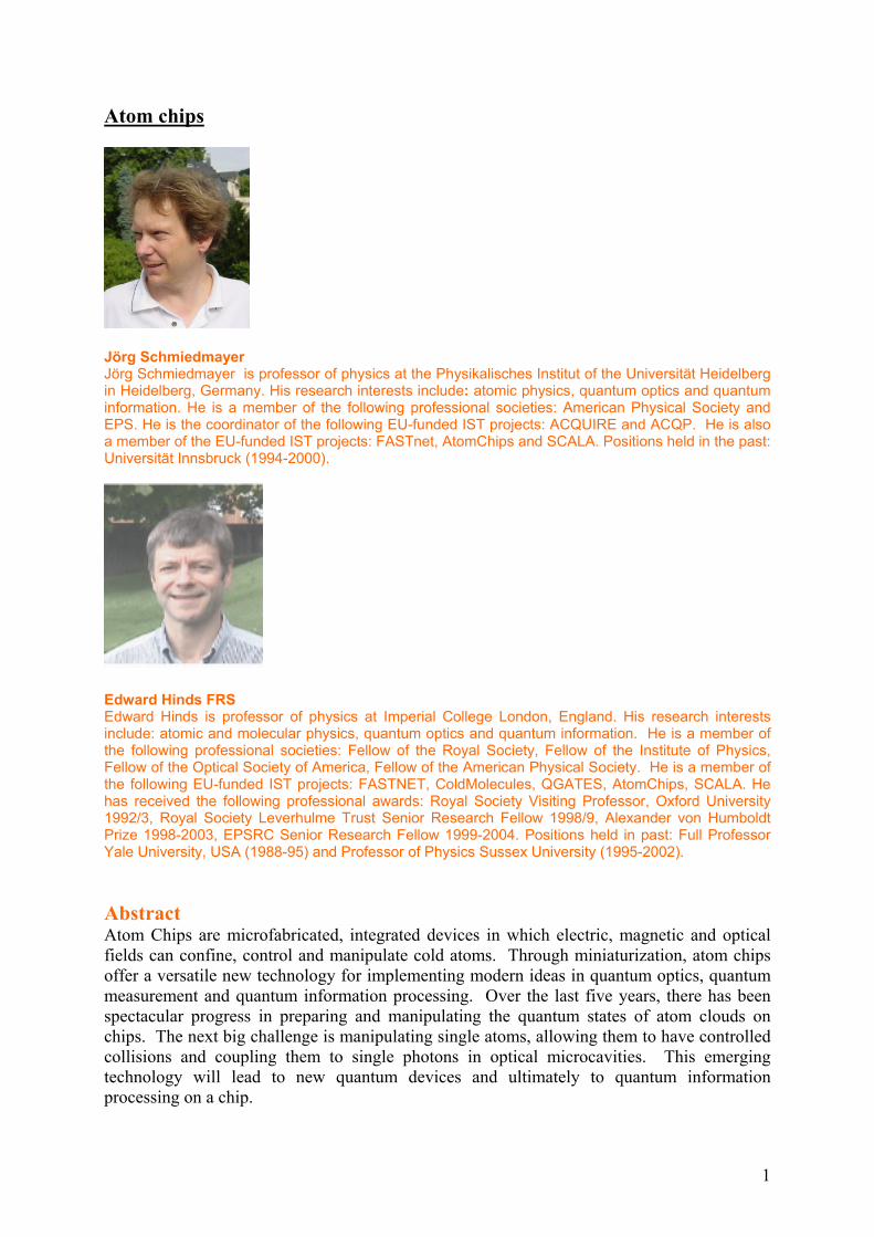
Atom chips
Jörg Schmiedmayer Jörg Schmiedmayer is professor of physics at the Physikalisches Institut of the Universität Heidelberg in Heidelberg, Germany. His research interests include: atomic physics, quantum optics and quantum information. He is a member of the following professional societies: American Physical Society and EPS. He is the coordinator of the following EU-funded IST projects: ACQUIRE and ACQP. He is also a member of the EU-funded IST projects: FASTnet, AtomChips and SCALA. Positions held in the past: Universität Innsbruck (1994-2000).
Edward Hinds FRS Edward Hinds is professor of physics at Imperial College London, England. His research interests include: atomic and molecular physics, quantum optics and quantum information. He is a member of the following professional societies: Fellow of the Royal Society, Fellow of the Institute of Physics, Fellow of the Optical Society of America, Fellow of the American Physical Society. He is a member of the following EU-funded IST projects: FASTNET, ColdMolecules, QGATES, AtomChips, SCALA. He has received the following professional awards: Royal Society Visiting Professor, Oxford University 1992/3, Royal Society Leverhulme Trust Senior Research Fellow 1998/9, Alexander von Humboldt Prize 1998-2003, EPSRC Senior Research Fellow 1999-2004. Positions held in past: Full Professor Yale University, USA (1988-95) and Professor of Physics Sussex University (1995-2002). Abstract Atom Chips are microfabricated, integrated devices in which electric, magnetic and optical fields can confine, control and manipulate cold atoms. Through miniaturization, atom chips offer a versatile new technology for implementing modern ideas in quantum optics, quantum measurement and quantum information processing. Over the last five years, there has been spectacular progress in preparing and manipulating the quantum states of atom clouds on chips. The next big challenge is manipulating single atoms, allowing them to have controlled collisions and coupling them to single photons in optical microcavities. This emerging technology will lead to new quantum devices and ultimately to quantum information processing on a chip.
1
Introduction Scientific and technological progress in the last decades has shown that miniaturization and integration can lead to robust applications of fundamental physics, be it electronics and semiconductor physics in integrated circuits and data processing, or optics in micro-optical devices, sensors and communication. Atom Chips are starting to realize a similar practical advance for quantum optical systems based on neutral atoms and photons. In micro electronics, electrons move through micro fabricated wires, switches, transistors, etc. in electronic integrated circuits, chips, to perform elaborate tasks. In Atom Chips, atoms are trapped above a surface, and forces under our control manipulate their motion and internal states. These forces are due to electric, magnetic and optical fields which originate in microscopic structures built on the surface of the chip. The forces produced in this way can confine atoms to micrometer-sized regions, where the characteristic quantum energy h2/2Ma2 (h is Planck’s constant, M is the mass of the atom and a is the 1 µm size of the trap) corresponds to a temperature of a few hundred nanoKelvins. Since the atoms can be much colder than this, quantum effects can be completely dominant, opening the possibility of new quantum devices based on the control of neutral atoms. This quantum confinement idea is precisely the one used to harness the electrons in mesoscopic quantum electronic devices. However, the atoms here are very well isolated from the warm solid state environment, allowing their quantum states to remain undisturbed for tens or hundreds of seconds. The combination of this long decoherence time together with the capability of precise microscopic control makes the atom chip an exceedingly attractive candidate for robust implementation of new quantum devices. Breadth of applicability Research over the last five years has already established the atom chip as an immensely versatile new technology able to perform an astonishing range of functions. Already we know how to collect atoms, cool them to nK temperatures and load them into tiny traps a few microns above the surface of the chip. Several groups now have Bose Einstein condensates (BEC) on a chip, in which some 10,000 atoms all have precisely the same wavefunction. This is a pure quantum state, similar to that of the light in a laser beam and it provides a crucial starting point for many quantum devices, including a quantum information processor, because it is a state of essentially no entropy. After several years of intense development, techniques have emerged for making electric, magnetic and optical fields drive coherent manipulations of this quantum state. Much of this development has focussed on understanding and controlling the decoherence processes due to fluctuations of the fields and the fundamentals now seem to be understood. Thus we now have some key ingredients of a powerful and versatile new technology capable of preparing and manipulating complex quantum states of atomic ensembles on a chip. With this toolbox in hand, the research community is well placed to realise many of the beautiful new ideas of quantum control and quantum information that have emerged over the last decade. For example, experiments on atoms in large optical lattices and cavities have shown how to prepare strings of single atoms and how to transfer quantum information coherently between atoms and photons. This could now be implemented on a chip, using the atom string as a quantum information register, and the atom-cavity coupling as a simple quantum interconnect providing optical readout. Suitable time-dependent fields should be able to manipulate the qubits to make them perform quantum logic operations. Although atom chips have only just begun to work, we can see now how all this might be integrated into a single
2
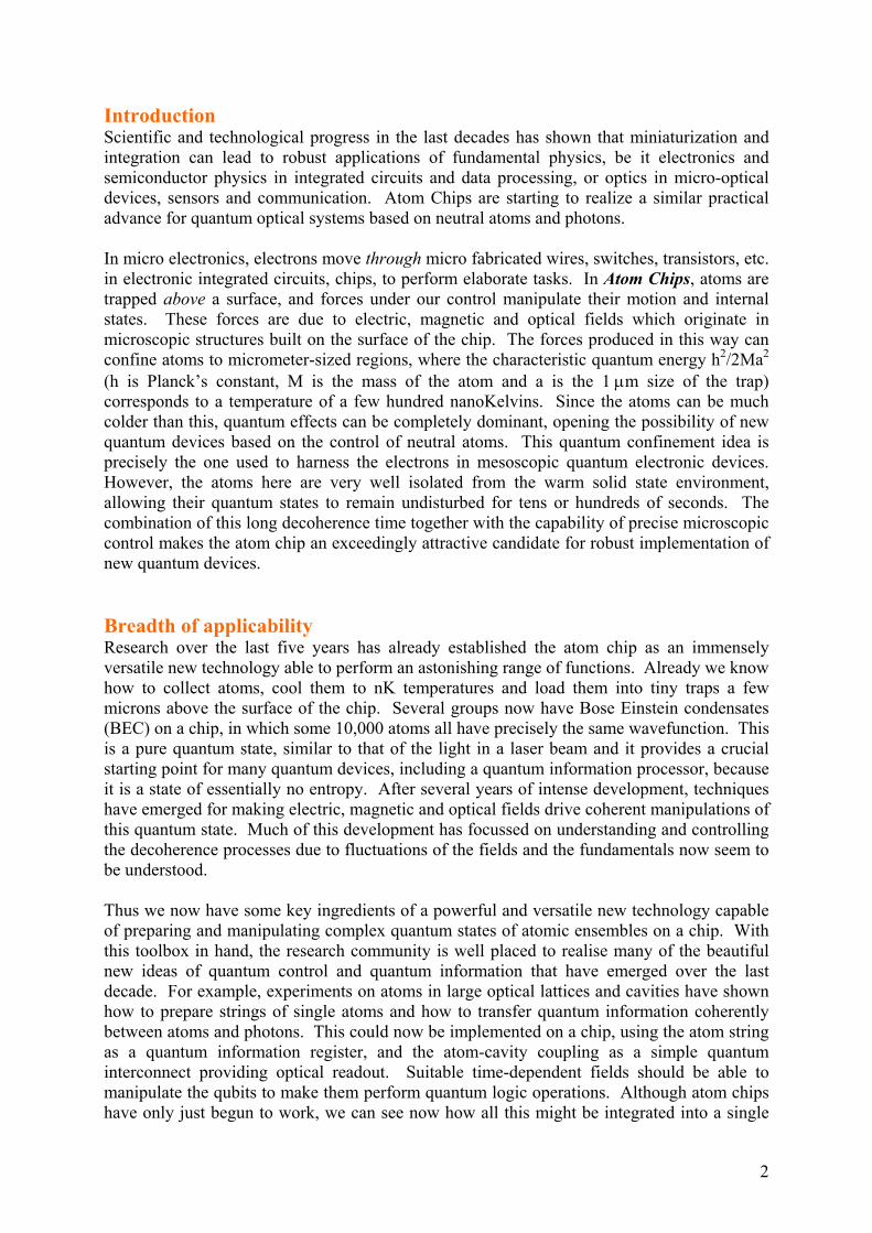
device. This is a daunting task, but it is also an exciting one with spectacular promise for future technology. Micro Traps Magnetic fields produced on the chip can manipulate a neutral atom by exerting forces on its magnetic dipole moment. For example, if a wire on the surface of the chip carries a current I this makes a magnetic field that loops around the wire, as illustrated in Figure 1. If a uniform field B is added to this, a line of zero net magnetic field forms parallel to the wire, as shown by the dashed line. The energy of a magnetic atom – one with electron spin, such as lithium or rubidium - is proportional to the strength of the field. Thus the atom moves on a potential surface, indicated by the mesh in the figure, which traps atoms along the dashed line at a distance R from the wire. This distance can be controlled by adjusting the current I or the field B. The force that pushes atoms to the centre of the trap is proportional to R-2, which means that miniature traps with a small value of R can hold atoms very tightly, reaching nanometer scales of confinement with very low levels of power dissipation.
Figure 1 Electric fields can also be used to control the atoms through the electric dipole interaction. Atoms are attracted to static fields and to low-frequency light fields. If the frequency of the light is increased to lie above an atomic resonance, the atom can be pushed away from the light. Using a standing wave it is particularly simple to make a closely-spaced array of traps, since the atoms are attracted to each of the antinodes or nodes. Oscillating fields (optical, microwave or radiofrequency) also make it possible to manipulate the internal states of an atom, where quantum information is most securely stored. For example, quantum oscillations in the hyperfine sublevels of a Cs atom are the basis of the atomic clock, which is so stable it provides the international definition of the second. Atomic clocks on a chip are already a reality.
3
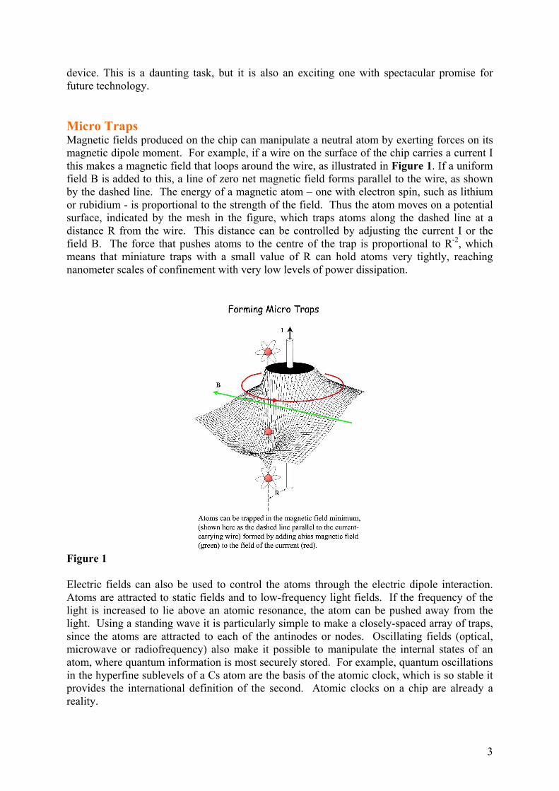
The full potential of atom chips for quantum applications is only accessible if the structures can be miniaturized to a scale of order 1 µm or below. This will allow atoms and photons to be coupled in a coherent way by placing atoms in a specific part of a light field. It will also allow tunneling between separated traps to make controlled atom-atom interactions. Researchers are working intensively on developing smaller electric and magnetic structures and on integrating new components such as micro-optics and micro-cavities into atom chips. Fabrication of Atom Chips Structures for magnetic and electric micro manipulation of neutral atoms benefit from being fabricated on a surface. They can be made much smaller and more robust than free-standing structures. Heat is dissipated easily through the substrate, allowing significantly higher currents to be sent through thin wires, and this results in tighter confinement and more precise control of the atoms. Micro-fabrication on a surface also permits precise positioning, as required in complex circuits with several different electric, magnetic or optical components. Combining, adapting and developing diverse fabrication technologies is therefore a central research activity. A very promising technique for fabricating high quality wires on an atom chip has been developed within the framework of ACQUIRE and ACQP collaborations. The best results so far have come from Au layers on Si single crystal substrates. State-of-the-art multi-layer structures, with feature sizes less than 500nm and with very smooth wires, allow large current densities (up to 108 A/cm2 for sub-µm wires at room temperature) and electric fields (up to 500V of potential difference over a ~10µm gap). The wires structures that are now being made have the capability of confining neutral atoms at trap frequencies up to 1 MHz, corresponding to a confinement length of ~10nm. A typical atom chip set-up ready to be mounted into the UHV chamber of the experiment and an electron microscope picture of a detailed structure on an ACQP chip are shown in Figure 2.
Figure 2 Magnetic atom chips are also being made using permanent magnetic microstructures. The first experiments used commercial magnetic storage media, such as floppy disks, video tape and hard disks. Bose-Einstein condensates have been loaded in such chips and versatile manipulations have been demonstrated with the help of adjustable bias fields. Now, custom-
4
built Pt/Co multilayer thin films are being developed within the QGates and FASTnet projects. As no real current flows in these films, they can make atom traps with very low technical and thermal noise. Super conducting structures at low temperature also offer low noise. In addition, the low temperature environment should be suitable for manipulating Rydberg atoms and may allow the coupling of neutral atoms to solid state quantum devices.
Quantum-Coherent Manipulation of Atoms It is remarkable that atoms at temperatures in the nanoKelvin range can be placed a few micrometers from a room temperature surface and retain their quantum coherence for many seconds. The influence of the nearby surface on quantum manipulation can be divided into two categories. [1] The surface of the chip has electromagnetic modes that are thermally excited. The resulting field noise above the chip can induce motion of the atoms and can flip their spins, leading to decoherence of the quantum state. [2] The materials of the chip and the method of fabrication leave imperfections of the structure that in turn cause imperfections in the atom-trapping potentials. From experiments conducted over the last five years within the ACQUIRE, ACQP, FASTnet and QGates collaborations we now know how to design and fabricate chips that keep all these effects under control.
A beautiful experiment done in Munich shows the quantum coherence that can be achieved using atoms on a chip. Here 87Rb atoms were magnetically trapped in a superposition of the two hyperfine ground states |F=1, mF=-1> and |F=2, mF=1>. These states differ in energy by 6.8GHz, causing the phase of the superposition to oscillate at that frequency. Figure 3 shows a Rubidium atomic clock on a chip. The beat between the atomic oscillation and a stable reference clock, demonstrates the long coherence time (>2.8 s) The long term stability of the clock was not limited by decoherence, but by the local reference oscillator. This shows that atom chips are suitable for practical quantum instruments. In terms of quantum information processing, the clock is an example of quantum-coherent single qubit manipulations. The next big challenge is to manipulate the interactions between atoms to produce controlled entanglement.
5
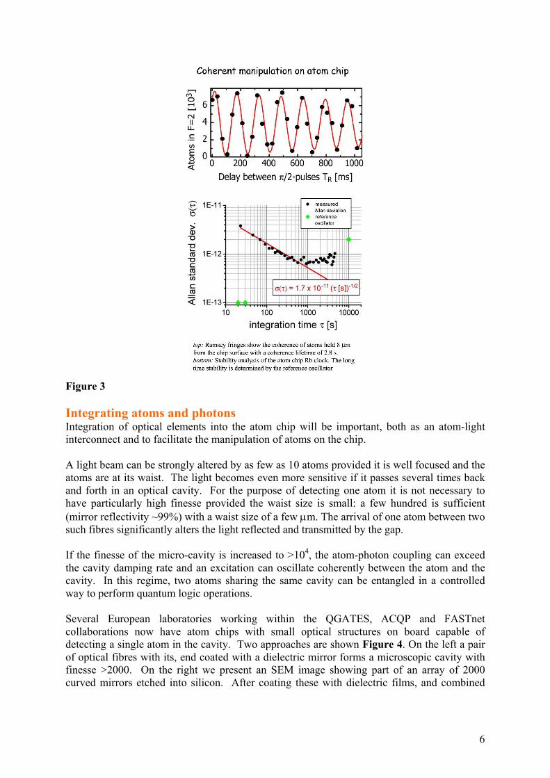
Figure 3 Integrating atoms and photons Integration of optical elements into the atom chip will be important, both as an atom-light interconnect and to facilitate the manipulation of atoms on the chip. A light beam can be strongly altered by as few as 10 atoms provided it is well focused and the atoms are at its waist. The light becomes even more sensitive if it passes several times back and forth in an optical cavity. For the purpose of detecting one atom it is not necessary to have particularly high finesse provided the waist size is small: a few hundred is sufficient (mirror reflectivity ~99%) with a waist size of a few µm. The arrival of one atom between two such fibres significantly alters the light reflected and transmitted by the gap. If the finesse of the micro-cavity is increased to >104, the atom-photon coupling can exceed the cavity damping rate and an excitation can oscillate coherently between the atom and the cavity. In this regime, two atoms sharing the same cavity can be entangled in a controlled way to perform quantum logic operations. Several European laboratories working within the QGATES, ACQP and FASTnet collaborations now have atom chips with small optical structures on board capable of detecting a single atom in the cavity. Two approaches are shown Figure 4. On the left a pair of optical fibres with its, end coated with a dielectric mirror forms a microscopic cavity with finesse >2000. On the right we present an SEM image showing part of an array of 2000 curved mirrors etched into silicon. After coating these with dielectric films, and combined
6
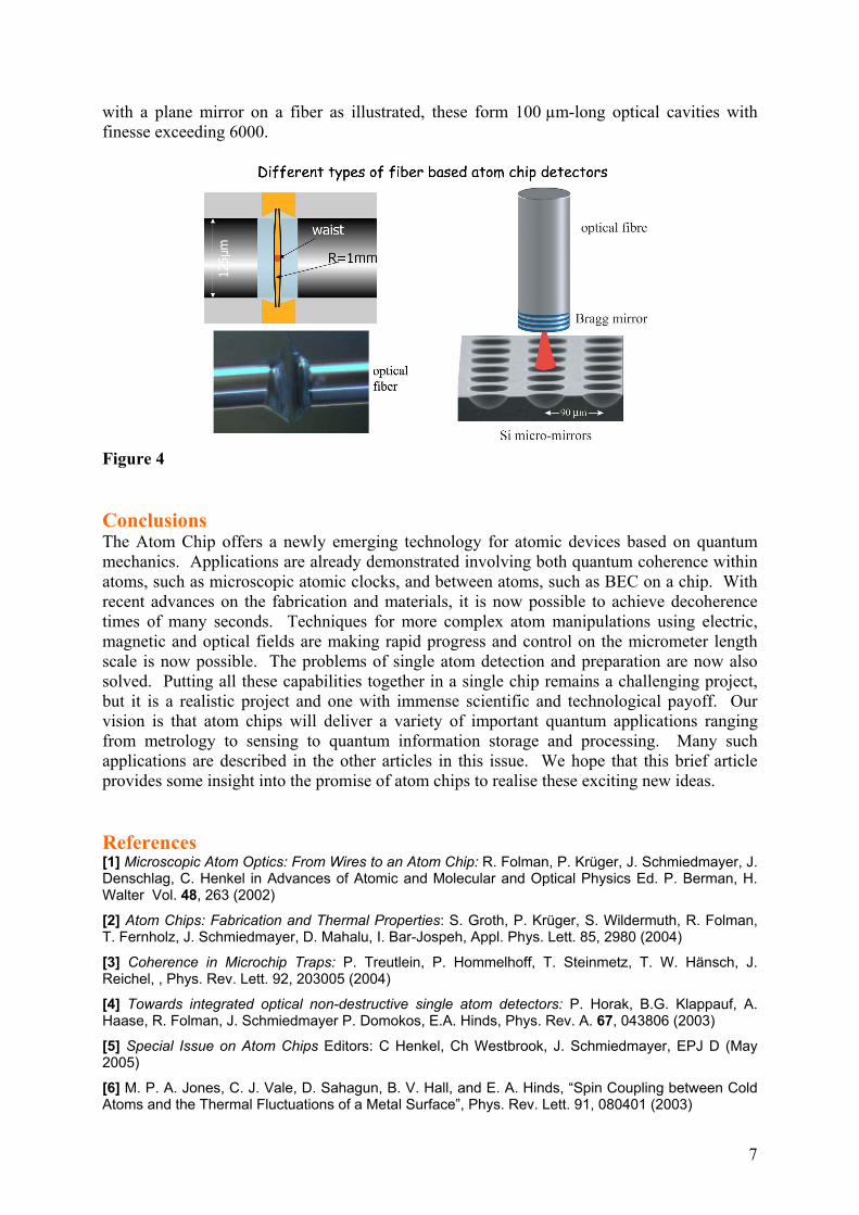
with a plane mirror on a fiber as illustrated, these form 100 µm-long optical cavities with finesse exceeding 6000.
Figure 4 Conclusions The Atom Chip offers a newly emerging technology for atomic devices based on quantum mechanics. Applications are already demonstrated involving both quantum coherence within atoms, such as microscopic atomic clocks, and between atoms, such as BEC on a chip. With recent advances on the fabrication and materials, it is now possible to achieve decoherence times of many seconds. Techniques for more complex atom manipulations using electric, magnetic and optical fields are making rapid progress and control on the micrometer length scale is now possible. The problems of single atom detection and preparation are now also solved. Putting all these capabilities together in a single chip remains a challenging project, but it is a realistic project and one with immense scientific and technological payoff. Our vision is that atom chips will deliver a variety of important quantum applications ranging from metrology to sensing to quantum information storage and processing. Many such applications are described in the other articles in this issue. We hope that this brief article provides some insight into the promise of atom chips to realise these exciting new ideas. References [1] Microscopic Atom Optics: From Wires to an Atom Chip: R. Folman, P. Krüger, J. Schmiedmayer, J. Denschlag, C. Henkel in Advances of Atomic and Molecular and Optical Physics Ed. P. Berman, H. Walter Vol. 48, 263 (2002)
[2] Atom Chips: Fabrication and Thermal Properties: S. Groth, P. Krüger, S. Wildermuth, R. Folman, T. Fernholz, J. Schmiedmayer, D. Mahalu, I. Bar-Jospeh, Appl. Phys. Lett. 85, 2980 (2004)
[3] Coherence in Microchip Traps: P. Treutlein, P. Hommelhoff, T. Steinmetz, T. W. Hänsch, J. Reichel, , Phys. Rev. Lett. 92, 203005 (2004)
[4] Towards integrated optical non-destructive single atom detectors: P. Horak, B.G. Klappauf, A. Haase, R. Folman, J. Schmiedmayer P. Domokos, E.A. Hinds, Phys. Rev. A. 67, 043806 (2003)
[5] Special Issue on Atom Chips Editors: C Henkel, Ch Westbrook, J. Schmiedmayer, EPJ D (May 2005)
[6] M. P. A. Jones, C. J. Vale, D. Sahagun, B. V. Hall, and E. A. Hinds, “Spin Coupling between Cold Atoms and the Thermal Fluctuations of a Metal Surface”, Phys. Rev. Lett. 91, 080401 (2003)
7
[7] M. P. A. Jones, C. J. Vale, D. Sahagun, B. V. Hall, C. C. Eberlein, B. E. Sauer, K. Furusawa, D. Richardson, and E. A. Hinds, “Cold atoms probe the magnetic field near a wire”, J. Phys B 37, L15 (2004)
[8] P.K. Rekdal, S. Scheel, P.L. Knight and E.A. Hinds, “Thermal spin-flips in atom chips”, Phys Rev A 70 013811 (2004) [9] S. Eriksson, F. Ramirez-Martinez, E.A. Curtis, B.E. Sauer, P.W. Nutter, E.W. Hill and E.A. Hinds, “Micron-sized atom traps made from magneto-optical thin films” Appl Phys B 79, 811 (2004)
[10] Moktadir, Z., Kukharenka, A., Kraft, M., Bagnall, D. M., Jones, M., Powell, H. and Hinds, E. A. “Etching techniques for the realization of optical micro-cavities on silicon for atom traps”. J. Micromech. Microeng. 14, 1 (2004) Projects funded by the European Commission and related to the work in this article: ACQUIRE Advanced quantum information research Start date: 01/01/1996 End date: 30/06/1999 Project web site: http://www.acquire.uni-hd.de/ Contact person: Elisabeth Giacobino, ENS Laboratoire Kastler-Brossel, Paris ACQP Atom Chip Quantum Processor Start date: 01/01/2003 End date: 31/12/2005 Project web site: http://acqp.physi.uni-heidelberg.de/ Contact person: Hannes jorg Schmiedmayer, Ruprecht-Karls-Universitaet Heidelberg, [email protected] FASTNET ColdMolecules Project web site: http://www.lac.u-psud.fr/coldmolecules/network/index.html QGATES Quantum Gates and Elementary Scalable Processors Using Deterministically Addressed Atoms Start date: 01/01/2003 End date: 31/12/2005 Project web site: http://www.ph.imperial.ac.uk/qgates/Contact person: Peter Knight, Imperial College of Science, technology and Medecine, [email protected] AtomChips Project web site: http://www.iota.u-psud.fr/~atomchip/ SCALA: FP6 Integrated Project in the process of negotiations. Scalable Quantum computing with Light and Atoms Contact person: Philippe Grangier, CNRS, [email protected] Projects funded by National initiatives or organizations and related to the work in this article: DFG Forschungsschwepunkte: Quanteninformation, Wechselwirkung in entarteten Quantengasen, Kompetenznetzwerk Quantninformation (Baaden Wuertemberg) EPSRC Cold Atoms in Microtraps Programme, UK Quantum Information IRC, UK Cold Atoms Network, UK Quantum Devices Network, Australian Centre for Quantum Atom Optics.
8
Contact information of the authors of this article: Prof. Dr. Joerg Schmiedmayer Universitaet Heidelberg Physikalisches Institut Philosophenweg 12 69120 Heidelberg Germany Tel: 49 6221 549 325 Fax: 49 6221 47 57 33 Email: [email protected] Prof. Edward Hinds Imperial College of Science, Technology and Medecine Quantum Optics & Laser Science Group Department of Physics Blackett Laboratory South Kensington Campus London SW7 2AZ Tel+ 44 (0)20 7594 7901 Email: [email protected]
9