Embed Size (px)
Citation preview

ATWINC1500-MR210PB DATASHEET
IEEE 802.11 b/g/n IoT Module
DATASHEET
Description
The ATWINC1500-MR210PB is a low-power consumption 802.11 b/g/n IoT (Internet
of Things) module, which is specifically optimized for low power IoT applications. The
highly integrated module features small form factor (21.5mm x 14.5mm x 2.1mm)
while fully integrating Power Amplifier, LNA, Switch, Power Management, and PCB
antenna. With seamless roaming capabilities and advanced security, it could be
interoperable with various vendors’ 802.11b/g/n Access Points in wireless LAN. The
module provides SPI and UART to interface to host controller.
Features
IEEE® 802.11 b/g/n 20MHz (1x1) solution
Single spatial stream in 2.4GHz ISM band
Integrated PA and T/R Switch
Integrated PCB antenna
Superior Sensitivity and Range via advanced PHY signal processing
Advanced Equalization and Channel Estimation
Advanced Carrier and Timing Synchronization
Wi-Fi Direct and Soft-AP support
Supports IEEE 802.11 WEP, WPA, WPA2 Security
Supports China WAPI security
Superior MAC throughput via hardware accelerated two-level A-MSDU/A-MPDU
frame aggregation and block acknowledgement
On-chip memory management engine to reduce host load
SPI, UART, and I2C host interfaces
2- or 3-wire Bluetooth® coexistence interface
Operating temperature range of -40°C to +85°C
I/O operating voltage of 2.7V to 3.6V
Integrated Flash memory for system software
Power Save Modes
– <4µA Power Down mode typical @3.3V I/O
– 380µA Doze mode with chip settings preserved (used for beacon monitoring)1
1See Power Consumption for module power modes.
Atmel-42502B-ATWINC1500-MR210PB-SmartConnect-Datasheet_02/2016

ATWINC1500-MR210P [DATASHEET] Atmel-42502B-ATWINC1500-MR210PB-SmartConnect-Datasheet_02/2016 2
2
– On-chip low power sleep oscillator
– Fast host wake-up from Doze mode by a pin or SPI transaction
Fast Boot Options
– On-chip Boot ROM (Firmware instant boot)
– SPI flash boot (firmware patches and state variables)
– Low-leakage on-chip memory for state variables
– Fast AP Re-Association (150ms)
On-Chip Network Stack to offload MCU
– Integrated Network IP stack to minimize host CPU requirements
– Network features TCP, UDP, DHCP, ARP, HTTP, SSL, and DNS
Hardware accelerators for Wi-Fi and SSL security to improve connection time
Hardware accelerator for IP checksum
Hardware accelerators for OTA security
Small footprint host driver (4KB flash – less than 1KB RAM)

Atmel-42502B-ATWINC1500-MR210PB-SmartConnect-Datasheet_02/2016
ATWINC1500-MR210PB [DATASHEET
3
Table of Contents
1 Ordering Information and Module Marking ................................................................ 5
2 Block Diagram ............................................................................................................. 6
3 Pinout Information ....................................................................................................... 7
3.1 Pin Description ...................................................................................................................................... 7
3.2 Module Outline Drawing ........................................................................................................................ 9
4 Electrical Specifications ........................................................................................... 10
4.1 Absolute Ratings ................................................................................................................................. 10
4.2 Recommended Operating Conditions ................................................................................................. 10
5 CPU and Memory Subsystems ................................................................................. 11
5.1 Processor ............................................................................................................................................ 11
5.2 Memory Subsystem............................................................................................................................. 11
5.3 Non-volatile Memory (eFuse) .............................................................................................................. 11
6 WLAN Subsystem ...................................................................................................... 12
6.1 MAC ............................................................................................................................................... 12
6.1.1 Features ................................................................................................................................. 12
6.1.2 Description .............................................................................................................................. 12
6.2 PHY ............................................................................................................................................... 13
6.2.1 Features ................................................................................................................................. 13
6.2.2 Description .............................................................................................................................. 13
6.3 Radio ............................................................................................................................................... 13
6.3.1 Receiver Performance ............................................................................................................ 14
6.3.2 Transmitter Performance ........................................................................................................ 15
7 External Interfaces .................................................................................................... 16
7.1 SPI Interface ....................................................................................................................................... 16
7.1.1 Overview................................................................................................................................. 16
7.1.2 SPI Timing .............................................................................................................................. 16
7.2 UART Interface ................................................................................................................................... 18
7.3 Wi-Fi/Bluetooth Coexistence ............................................................................................................... 18
8 Power Consumption .................................................................................................. 19
8.1 Description of Device States ............................................................................................................... 19
8.2 Current Consumption in Various Device States .................................................................................. 19
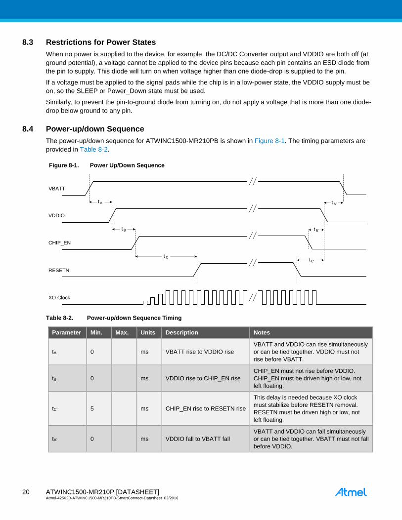
8.3 Restrictions for Power States .............................................................................................................. 20
8.4 Power-up/down Sequence .................................................................................................................. 20
8.5 Digital I/O Pin Behavior During Power-up Sequences......................................................................... 21
9 Notes On Interfacing to the ATWINC1500-MR210PB .............................................. 22
9.1 Programmable Pull-up Resistors ......................................................................................................... 22
10 RF Performance Placement Guidelines ................................................................... 22
11 Schematic Design Information ................................................................................. 23
11.1 Application Schematic ......................................................................................................................... 23
12 Reflow Profile Information ........................................................................................ 24

ATWINC1500-MR210P [DATASHEET] Atmel-42502B-ATWINC1500-MR210PB-SmartConnect-Datasheet_02/2016 4
4
12.1 Storage Condition................................................................................................................................ 24
12.1.1 Moisture Barrier Bag Before Opened ..................................................................................... 24
12.1.2 Moisture Barrier Bag Open ..................................................................................................... 24
12.2 Stencil Design ..................................................................................................................................... 24
12.3 Baking Conditions ............................................................................................................................... 24
12.4 Soldering and Reflow Condition .......................................................................................................... 24
12.4.1 Reflow Oven ........................................................................................................................... 24
13 Reference Documentation and Support................................................................... 26
13.1 Reference Documents ......................................................................................................................... 26
14 Revision History ........................................................................................................ 27

Atmel-42502B-ATWINC1500-MR210PB-SmartConnect-Datasheet_02/2016
ATWINC1500-MR210PB [DATASHEET
5
1 Ordering Information and Module Marking
Table 1-1. Ordering Details
Ordering code Package Description
ATWINC1500-MR210PB 22x15mm Certified module with ATWINC1500B chip and PCB antenna
ATWINC1500-MR210UB 22x15mm Certified module with ATWINC1500B chip and uFL connector
ATWINC1510-MR210PB 22x15mm Certified module with ATWINC1510B chip (8Mb Flash) and
PCB antenna
Figure 1-1. Marking Information

ATWINC1500-MR210P [DATASHEET] Atmel-42502B-ATWINC1500-MR210PB-SmartConnect-Datasheet_02/2016 6
6
2 Block Diagram
Figure 2-1. Block Diagram of the Module

Atmel-42502B-ATWINC1500-MR210PB-SmartConnect-Datasheet_02/2016
ATWINC1500-MR210PB [DATASHEET
7
3 Pinout Information
3.1 Pin Description
Figure 3-1. Pin Assignment
Table 3-1. Pin Description
NO Name Type Description Programmable
pull-up resistor
1 GPIO_6 I/O General purpose I/O Yes
2 I2C_SCL I/O I2C Slave Clock. Currently used only for Atmel debug. Not for cus-
tomer use. Leave unconnected. Yes
3 I2C_SDA I/O I2C Slave Data. Currently used only for Atmel debug. Not for customer
use. Leave unconnected. Yes
4 RESET_N I
Active-Low Hard Reset. When asserted to a low level, the module will
be placed in a reset state. When asserted to a high level, the module
will run normally. Connect to a host output that defaults low at power
up. If the host output is tri-stated, add a 1MΩ pull-down resistor to en-
sure a low level at power up.
No
5 NC - No connect

ATWINC1500-MR210P [DATASHEET] Atmel-42502B-ATWINC1500-MR210PB-SmartConnect-Datasheet_02/2016 8
8
NO Name Type Description Programmable
pull-up resistor
6 NC - No connect
7 NC - No connect
8 NC - No connect
9 GND_1 - GND
10 SPI_CFG I Tie to VDDIO through a 1MΩ resistor to enable the SPI interface No
11 WAKE I Host Wake control. Can be used to wake up the module from Doze
mode. Connect to a host GPIO. Yes
12 GND_2 - GND
13 IRQN O ATWINC1500-MR210P Device Interrupt output. Connect to host inter-
rupt input pin. Yes
14 UART_TXD O UART Transmit Output from ATWINC1500-MR210P Yes
15 SPI_RXD I SPI MOSI (Master Out Slave In) pin Yes
16 SPI_SSN I SPI Slave Select. Active low Yes
17 SPI_TXD O SPI MISO (Master In Slave Out) pin Yes
18 SPI_SCK I SPI Clock Yes
19 UART_RXD I UART Receive input to ATWINC1500-MR210P Yes
20 VBATT - Battery power supply
21 GPIO_1/RTC I General Purpose I/O / RTC Yes
22 CHIP_EN I
Module enable. High level enables module, low level places module in
Power Down mode. Connect to a host Output that defaults low at
power up. If the host output is tri-stated, add a 1MΩ pull-down resistor
to ensure a low level at power up.
No
23 VDDIO - I/O Power Supply. Must match host I/O voltage.
24 1P3V_TP - 1.3V VDD Core Test Point. Leave unconnected.
25 GPIO_3 I/O General purpose I/O
26 GPIO_4 I/O General purpose I/O Yes
27 GPIO_5 I/O General purpose I/O Yes
28 GND_3 - GND
29 PADDLE - GND

Atmel-42502B-ATWINC1500-MR210PB-SmartConnect-Datasheet_02/2016
ATWINC1500-MR210PB [DATASHEET
9
3.2 Module Outline Drawing
Figure 3-2. Module Drawings – ATWINC1500-MR210PB - Top and Bottom Views (unit = mm)
NOTE: THIS PAD MUST BE
SOLDERED TO GND.
NOTE: THIS PAD MUST BE
SOLDERED TO GND.
Figure 3-3. Module Drawings – ATWINC1500-MR210UB - Top and Bottom Views (unit = mm)
NOTE:THIS PAD MUST BE
SOLDERED TO GND.
NOTE: THIS PAD MUST BE
SOLDERED TO GND.

ATWINC1500-MR210P [DATASHEET] Atmel-42502B-ATWINC1500-MR210PB-SmartConnect-Datasheet_02/2016 1
0
10
4 Electrical Specifications
4.1 Absolute Ratings
Table 4-1. Voltages
Symbol Description Min. Max. Unit
VBATT Input supply voltage -0.3 5.0 V
VDDIO I/O voltage -0.3 4.6 V
4.2 Recommended Operating Conditions
Table 4-2. Recommended Operating Conditions
Test conditions: -40ºC - +85ºC
Symbol Min. Typ. Max. Unit
VBATT 3.0 3.6 4.2 V
VDDIO 2.7 3.3 3.6 V

Atmel-42502B-ATWINC1500-MR210PB-SmartConnect-Datasheet_02/2016
ATWINC1500-MR210PB [DATASHEET
11
5 CPU and Memory Subsystems
5.1 Processor
ATWINC1500B has a Cortus APS3 32-bit processor. This processor performs many of the MAC functions,
including but not limited to association, authentication, power management, security key management, and MSDU
aggregation/de-aggregation. In addition, the processor provides flexibility for various modes of operation, such as
STA and AP modes.
5.2 Memory Subsystem
The APS3 core uses a 128KB instruction/boot ROM along with a 160KB instruction RAM and a 64KB data RAM.
ATWINC1500B also has 4Mb of flash memory, which can be used for system software. In addition, the device
uses a 128KB shared RAM, accessible by the processor and MAC, which allows the APS3 core to perform various
data management tasks on the TX and RX data packets.
5.3 Non-volatile Memory (eFuse)
ATWINC1500B has 768 bits of non-volatile eFuse memory that can be read by the CPU after device reset. This
non-volatile one-time-programmable (OTP) memory can be used to store customer-specific parameters, such as
MAC address; various calibration information, such as TX power, crystal frequency offset, etc.; and other software-
specific configuration parameters. The eFuse is partitioned into six 128-bit banks. Each bank has the same bit
map, which is shown in Figure 5-1. The purpose of the first 80 bits in each bank is fixed, and the remaining 48 bits
are general-purpose software dependent bits, or reserved for future use. Since each bank can be programmed
independently, this allows for several updates of the device parameters following the initial programming, e.g.
updating MAC address. Refer to ATWINC1500-MR210PB Programming Guide for the eFuse programming
instructions.
Figure 5-1. eFuse Bit Map
Bank 0
Bank 1
Bank 2
Bank 3
Bank 4
Bank 5
F MAC ADDR
Use
d
Inva
lid
Ver
sio
n
Res
erve
d
MA
C A
DD
R
Use
d
FO
Flags
G
31 1 4 1
Use
d
TX
Ga
inC
orr
ecti
on
Use
d
Freq
. O
ffse
t
1 7
488 8 16
1 15
128 Bits

ATWINC1500-MR210P [DATASHEET] Atmel-42502B-ATWINC1500-MR210PB-SmartConnect-Datasheet_02/2016 1
2
12
6 WLAN Subsystem
The WLAN subsystem is composed of the Media Access Controller (MAC) and the Physical Layer (PHY). The
following two subsections describe the MAC and PHY in detail.
6.1 MAC
6.1.1 Features
The ATWINC1500-MR210PB IEEE802.11 MAC supports the following functions:
IEEE 802.11b/g/n
IEEE 802.11e WMM QoS EDCA/PCF multiple access categories traffic scheduling
Advanced IEEE 802.11n features:
– Transmission and reception of aggregated MPDUs (A-MPDU)
– Transmission and reception of aggregated MSDUs (A-MSDU)
– Immediate Block Acknowledgement
– Reduced Interframe Spacing (RIFS)
Support for IEEE802.11i and WFA security with key management
– WEP 64/128
– WPA-TKIP
– 128-bit WPA2 CCMP (AES)
Support for WAPI security
Advanced power management
– Standard 802.11 Power Save Mode
– Wi-Fi Alliance WMM-PS (U-APSD)
RTS-CTS and CTS-self support
Supports either STA or AP mode in the infrastructure basic service set mode
Supports independent basic service set (IBSS)
6.1.2 Description
The ATWINC1500B MAC is designed to operate at low power while providing high data throughput. The IEEE
802.11 MAC functions are implemented with a combination of dedicated datapath engines, hardwired control logic,
and a low-power, high-efficiency microprocessor. The combination of dedicated logic with a programmable
processor provides optimal power efficiency and real-time response while providing the flexibility to accommodate
evolving standards and future feature enhancements.
Dedicated datapath engines are used to implement datapath functions with heavy computational requirements. For
example, an FCS engine checks the CRC of the transmitting and receiving packets, and a cipher engine performs
all the required encryption and decryption operations for the WEP, WPA-TKIP, WPA2 CCMP-AES, and WAPI
security requirements.
Control functions which have real-time requirements are implemented using hardwired control logic modules.
These logic modules offer real-time response while maintaining configurability via the processor. Examples of
hardwired control logic modules are the channel access control module (implements EDCA/HCCA, Beacon TX
control, interframe spacing, etc.), protocol timer module (responsible for the Network Access Vector, back-off
timing, timing synchronization function, and slot management), MPDU handling module, aggregation/de-
aggregation module, block ACK controller (implements the protocol requirements for burst block communication),
and TX/RX control FSMs (coordinate data movement between PHY-MAC interface, cipher engine, and the DMA
interface to the TX/RX FIFOs).

Atmel-42502B-ATWINC1500-MR210PB-SmartConnect-Datasheet_02/2016
ATWINC1500-MR210PB [DATASHEET
13
The MAC functions implemented solely in software on the microprocessor have the following characteristics:
Functions with high memory requirements or complex data structures. Examples are association table
management and power save queuing.
Functions with low computational load or without critical real-time requirements. Examples are authentication
and association.
Functions which need flexibility and upgradeability. Examples are beacon frame processing and QoS
scheduling.
6.2 PHY
6.2.1 Features
The ATWINC1500B IEEE802.11 PHY supports the following functions:
Single antenna 1x1 stream in 20MHz channels
Supports IEEE 802.11b DSSS-CCK modulation: 1, 2, 5.5, 11Mbps
Supports IEEE 802.11g OFDM modulation: 6, 9, 12,18, 24, 36, 48, 54Mbps
Supports IEEE 802.11n HT modulations MCS0-7, 20MHz, 800 and 400ns guard interval: 6.5, 7.2, 13.0, 14.4,
19.5, 21.7, 26.0, 28.9, 39.0, 43.3, 52.0, 57.8, 58.5, 65.0, 72.2Mbps
IEEE 802.11n mixed mode operation
Per packet TX power control
Advanced channel estimation/equalization, automatic gain control, CCA, carrier/symbol recovery, and frame
detection
6.2.2 Description
The ATWINC1500BWLAN PHY is designed to achieve reliable and power-efficient physical layer communication
specified by IEEE 802.11 b/g/n in single stream mode with 20MHz bandwidth. Advanced algorithms have been
employed to achieve maximum throughput in a real world communication environment with impairments and
interference. The PHY implements all the required functions such as FFT, filtering, FEC (Viterbi decoder),
frequency, and timing acquisition and tracking, channel estimation and equalization, carrier sensing and clear
channel assessment, as well as the automatic gain control.
6.3 Radio
Table 6-1. Radio Performance under Typical Conditions: VBATT=3.3V; VDDIO=3.3V; temp.: 25ºC
Feature Description
Module Part Number ATWINC1500-MR210PB
WLAN Standard IEEE 802.11b/g/n, Wi-Fi compliant
Host Interface SPI, UART
Dimension L x W x H: 21.72 x 14.73 x 3.5 (typical) mm
Frequency Range 2.412GHz ~ 2.4835GHz (2.4GHz ISM Band)
Number of Channels 11 for North America, 13 for Europe, and 14 for Japan
Modulation 802.11b: DQPSK, DBPSK, CCK
802.11g/n: OFDM /64-QAM,16-QAM, QPSK, BPSK
Data Rate 802.11b: 1, 2, 5.5, 11Mbps
802.11g: 6, 9, 12, 18, 24, 36, 48, 54Mbps

ATWINC1500-MR210P [DATASHEET] Atmel-42502B-ATWINC1500-MR210PB-SmartConnect-Datasheet_02/2016 1
4
14
Feature Description
Data Rate
(20MHz, normal GI, 800ns) 802.11n: 6.5, 13, 19.5, 26, 39, 52, 58.5, 65Mbps
Data Rate
(20MHz, short GI, 400ns) 802.11n: 7.2, 14.4, 21.7, 28.9, 43.3, 57.8, 65,72.2Mbps
Operating temperature -40°C to 85°C
Storage temperature -40°C to 85°C
Humidity Operating Humidity 10% to 95% Non-Condensing
Storage Humidity 5% to 95% Non-Condensing
6.3.1 Receiver Performance
Radio performance under typical conditions: VBATT=3.3V; VDDIO=3.3V; temp.: 25°C.
Table 6-2. Receiver Performance
Parameter Description Minimum Typical Maximum Unit
Frequency 2,412 2,484 MHz
Sensitivity
802.11b
1Mbps DSS -98
dBm
2Mbps DSS -94
5.5Mbps DSS -92
11Mbps DSS -88
Sensitivity
802.11g
6Mbps OFDM -90
9Mbps OFDM -89
12Mbps OFDM -88
18Mbps OFDM -85
24Mbps OFDM -83
36Mbps OFDM -80
48Mbps OFDM -76
54Mbps OFDM -74
Sensitivity
802.11n
(BW=20MHz)
MCS 0 -89
MCS 1 -87
MCS 2 -85
MCS 3 -82
MCS 4 -77
MCS 5 -74
MCS 6 -72
MCS 7 -70.5
Maximum Receive
Signal Level
1-11Mbps DSS 0
6-54Mbps OFDM 0

Atmel-42502B-ATWINC1500-MR210PB-SmartConnect-Datasheet_02/2016
ATWINC1500-MR210PB [DATASHEET
15
Parameter Description Minimum Typical Maximum Unit
MCS 0 – 7 0
Adjacent Channel
Rejection
1Mbps DSS (30MHz offset) 50
dB
11Mbps DSS (25MHz offset) 43
6Mbps OFDM (25MHz offset) 40
54Mbps OFDM (25MHz offset) 25
MCS 0 – 20MHz BW (25MHz offset) 40
MCS 7 – 20MHz BW (25MHz offset) 20
Cellular Blocker
Immunity
776-794MHz CDMA -14
dBm
824-849MHz GSM -10
880-915MHz GSM -10
1710-1785MHz GSM -15
1850-1910MHz GSM -15
1850-1910MHz WCDMA -24
1920-1980MHz WCDMA -24
6.3.2 Transmitter Performance
Radio performance under typical conditions: VBATT=3.3V; VDDIO=3.3V; temp.: 25°C.
Table 6-3. Transmitter Performance
Parameter Description Minimum Typical Maximum Unit
Frequency 2,412 2,484 MHz
Output Power (1)
ON_Transmit
802.11b 1Mbps 18.5
dBm
802.11b 11Mbps 19.5
802.11g 6Mbps 18.5
802.11g 54Mbps 16.5
802.11n MCS 0 17.0
802.11n MCS 7 14.5
TX Power Accuracy ±1.5 (2) dB
Carrier Suppression 30.0 dBc
Harmonic Output Power 2nd -41
dBm/MHz 3rd -41
Notes: 1. Measured at 802.11 spec compliant EVM/Spectral Mask.
2. Measured after RF matching network. See reference design.

ATWINC1500-MR210P [DATASHEET] Atmel-42502B-ATWINC1500-MR210PB-SmartConnect-Datasheet_02/2016 1
6
16
7 External Interfaces
7.1 SPI Interface
7.1.1 Overview
ATWINC1500-MR210PB has a Serial Peripheral Interface (SPI) that operates as a SPI slave. The SPI interface
can be used for control and for serial I/O of 802.11 data. The SPI pins are mapped as shown in Table 7-1. The SPI
is a full-duplex slave-synchronous serial interface that is available immediately following reset when pin 10
(SPI_CFG) is tied to VDDIO.
Table 7-1. SPI Interface Pin Mapping
Pin # SPI function
10 CFG: Must be tied to VDDIO
16 SSN: Active Low Slave Select
15 MOSI(RXD): Serial Data Receive
18 SCK: Serial Clock
17 MISO(TXD): Serial Data Transmit
When the SPI is not selected, i.e., when SSN is high, the SPI interface will not interfere with data transfers
between the serial-master and other serial-slave devices. When the serial slave is not selected, its transmitted data
output is buffered, resulting in a high impedance drive onto the MISO line.
The SPI interface responds to a protocol that allows an external host to read or write any register in the chip as
well as initiate DMA transfers.
The SPI SSN, MOSI, MISO, and SCK pins of the ATWINC1500-MR210PB have internal programmable pull-up
resistors (See Section 9.1). These resistors should be programmed to be disabled. Otherwise, if any of the SPI
pins are driven to a low level while the ATWINC1500-MR210PB is in the low-power sleep state, the current will
flow from the VDDIO supply through the pull-up resistors, increasing the current consumption of the module.
7.1.2 SPI Timing
The SPI timing is provided in Figure 7-1 and Table 7-2.

Atmel-42502B-ATWINC1500-MR210PB-SmartConnect-Datasheet_02/2016
ATWINC1500-MR210PB [DATASHEET
17
Figure 7-1. SPI Timing Diagram (SPI Mode CPOL=0, CPHA=0)
tLH
SCK
TXD
RXD
SSN
tWH
tHL
tWL
tODLY
tISU tIHD
fSCK
tSSODLY
SSN
tSUSSN tHDSSN
SPI Master
SPI Slave
Table 7-2. SPI Slave Timing Parameters
Parameter Symbol Min. Max. Units Remarks
Clock Input Frequency fSCK 48 MHz
Clock Low Pulse Width tWL 5
ns
Clock High Pulse Width tWH 5
Clock Rise Time tLH 5
Clock Fall Time tHL 5
Input Setup Time tISU 5
Input Hold Time tIHD 5
Output Delay tODLY 0 20
Slave Select Setup Time tSUSSN 5
Slave Select Hold Time tHDSSN 5

ATWINC1500-MR210P [DATASHEET] Atmel-42502B-ATWINC1500-MR210PB-SmartConnect-Datasheet_02/2016 1
8
18
7.2 UART Interface
The ATWINC1500-MR210PB has a Universal Asynchronous Receiver/Transmitter (UART) interface available on
pins 14 and 19. It can be used for control or data transfer if the baud rate is sufficient for a given application. The
UART is compatible with the RS-232 standard, where ATWINC1500-MR210PB operates as Data Terminal
Equipment (DTE). It has a two-pin RXD/TXD interface.
The UART features programmable baud rate generation with fractional clock division, which allows transmission
and reception at a wide variety of standard and non-standard baud rates. The UART input clock is selectable
between 10MHz, 5MHz, 2.5MHz, and 1.25MHz. The clock divider value is programmable as 13 integer bits and 3
fractional bits (with 8.0 being the smallest recommended value for normal operation). This results in the maximum
supported baud rate of 10MHz/8.0 = 1.25MBd.
The UART can be configured for seven or eight bit operation, with or without parity, with four different parity types
(odd, even, mark, or space), and with one or two stop bits. It also has RX and TX FIFOs, which ensure reliable
high speed reception and low software overhead transmission. FIFO size is 4 x 8 for both RX and TX direction.
The UART also has status registers showing the number of received characters available in the FIFO and various
error conditions, as well the ability to generate interrupts based on these status bits.
An example of UART receiving or transmitting a single packet is shown in Figure 7-2. This example shows 7-bit
data (0x45), odd parity, and two stop bits.
See the ATWINC1500-MR210PB Programming Guide for information on configuring the UART.
Figure 7-2. Example of UART RX of TX Packet
7.3 Wi-Fi/Bluetooth Coexistence
ATWINC1500-MR210PB supports 2- and 3-wire Wi-Fi/Bluetooth Coexistence signaling conforming to the IEEE
802.15.2-2003 standard, Part 15.2. The type of coexistence interface used (2- or 3-wire) is chosen to be
compatible with the specific Bluetooth device used in a given application. Coexistence interface can be enabled on
the following pins: GPIO_1, GPIO_3, GPIO_4, GPIO_5, GPIO_6, I2C_SCL, I2C_SDA – each of these pins can be
configured for any function of the coexistence interface. Table 7-3 shows a usage example of the 2-wire interface
using the GPIO_3 and GPIO_4 pins; 3-wire interface using the GPIO_3, GPIO_4, and GPIO_5 pins; for more
specific instructions on configuring Coexistence refer to ATWINC1500-MR210PB Programming Guide.
Table 7-3. Coexistence Pin Assignment Example
Pin name Pin # Function Target 2-wire 3-wire
GPIO_3 25 BT_Req BT is requesting to access the medium to transmit or
receive. Goes high on TX or RX slot Used Used
GPIO_4 26 WL_Act Device response to the BT request. High - BT_req is
denied and BT slot blocked. Used Used
GPIO_5 27 BT_Pri Priority of the BT packets in the requested slot. High to
indicate high priority and low for normal. Not Used Used
GPIO_6 1 Ant_SW Direct control on Antenna (coex bypass) Optional Optional

Atmel-42502B-ATWINC1500-MR210PB-SmartConnect-Datasheet_02/2016
ATWINC1500-MR210PB [DATASHEET
19
8 Power Consumption
8.1 Description of Device States
ATWINC1500-MR210PB has several Devices States:
ON_Transmit – Device is actively transmitting an 802.11 signal. Highest output power and nominal current
consumption.
ON_Receive – Device is actively receiving an 802.11 signal. Lowest sensitivity and nominal current
consumption.
ON_Doze – Device is on but is neither transmitting nor receiving
Power_Down – Device core supply off (Leakage)
IDLE connect – Device is connected with 1 DTIM beacon interval
The following pins are used to switch between the ON and Power_Down states:
CHIP_EN – Device pin (pin #22) used to enable DC/DC Converter
VDDIO – I/O supply voltage from external supply
In the ON states, VDDIO is on and CHIP_EN is high (at VDDIO voltage level). To switch between the ON states
and Power_Down state CHIP_EN has to change between high and low (GND) voltage. When VDDIO is off and
CHIP_EN is low, the chip is powered off with no leakage (also see Section 8.3).
8.2 Current Consumption in Various Device States
Table 8-1. Current Consumption
Device state Code rate Output
power, dBm
Current consumption (1)
IVBATT IVDDIO
ON_Transmit
802.11b 1Mbps 19.5 294mA 22mA
802.11b 11Mbps 20.5 290mA 22mA
802.11g 6Mbps 19.5 292mA 22mA
802.11g 54Mbps 17.5 250mA 22mA
802.11n MCS 0 18.0 289mA 22mA
802.11n MCS 7 15.5 244mA 22mA
ON_Receive
802.11b 1Mbps N/A 52.5mA 22mA
802.11b 11Mbps N/A 52.5mA 22mA
802.11g 6Mbps N/A 55.0mA 22mA
802.11g 54Mbps N/A 57.5mA 22mA
802.11n MCS 0 N/A 54.0mA 22mA
802.11n MCS 7 N/A 58.5mA 22mA
ON_Doze N/A N/A 380µA <10µA
Power_Down N/A N/A <0.5µA <3.5µA
Notes: 1. Conditions: VBATT @ 3.6V, VDDIO@ 3.3V, temp. 25°C.
ATWINC1500-MR210P [DATASHEET] Atmel-42502B-ATWINC1500-MR210PB-SmartConnect-Datasheet_02/2016 2
0
20
8.3 Restrictions for Power States
When no power is supplied to the device, for example, the DC/DC Converter output and VDDIO are both off (at
ground potential), a voltage cannot be applied to the device pins because each pin contains an ESD diode from
the pin to supply. This diode will turn on when voltage higher than one diode-drop is supplied to the pin.
If a voltage must be applied to the signal pads while the chip is in a low-power state, the VDDIO supply must be
on, so the SLEEP or Power_Down state must be used.
Similarly, to prevent the pin-to-ground diode from turning on, do not apply a voltage that is more than one diode-
drop below ground to any pin.
8.4 Power-up/down Sequence
The power-up/down sequence for ATWINC1500-MR210PB is shown in Figure 8-1. The timing parameters are
provided in Table 8-2.
Figure 8-1. Power Up/Down Sequence
VBATT
VDDIO
CHIP_EN
RESETN
t A
t B
t C
XO Clock
t B'
t A'
tC'
Table 8-2. Power-up/down Sequence Timing
Parameter Min. Max. Units Description Notes
tA 0 ms VBATT rise to VDDIO rise
VBATT and VDDIO can rise simultaneously
or can be tied together. VDDIO must not
rise before VBATT.
tB 0 ms VDDIO rise to CHIP_EN rise
CHIP_EN must not rise before VDDIO.
CHIP_EN must be driven high or low, not
left floating.
tC 5 ms CHIP_EN rise to RESETN rise
This delay is needed because XO clock
must stabilize before RESETN removal.
RESETN must be driven high or low, not
left floating.
tA’ 0 ms VDDIO fall to VBATT fall
VBATT and VDDIO can fall simultaneously
or can be tied together. VBATT must not fall
before VDDIO.

Atmel-42502B-ATWINC1500-MR210PB-SmartConnect-Datasheet_02/2016
ATWINC1500-MR210PB [DATASHEET
21
Parameter Min. Max. Units Description Notes
tB’ 0 ms CHIP_EN fall to VDDIO fall
VDDIO must not fall before CHIP_EN.
CHIP_EN and RESETN can fall simultane-
ously.
tC’ 0 ms RESETN fall to VDDIO fall
VDDIO must not fall before RESETN. RE-
SETN and CHIP_EN can fall simultane-
ously.
8.5 Digital I/O Pin Behavior During Power-up Sequences
Table 8-3 represents digital I/O Pin states corresponding to device power modes.
Table 8-3. Digital I/O Pin Behavior in Different Device States
Device state VDDIO CHIP_EN RESETN Output
driver
Input
driver
Pull-up/down
resistor (96kΩ)
Power Down:
core supply off High Low Low Disabled (Hi-Z) Disabled Disabled
Power-On Reset:
core supply on, hard reset on High High Low Disabled (Hi-Z) Disabled Enabled
Power-On Default:
core supply on, device out of
reset but not programmed
yet
High High High Disabled (Hi-Z) Enabled Enabled
On Sleep/
On Transmit/
On Receive:
core supply on, device
programmed by firmware
High High High
Programmed by
firmware for
each pin:
Enabled or Dis-
abled
Opposite
of Output
Driver
state
Programmed by
firmware for
each pin:
Enabled or
Disabled

ATWINC1500-MR210P [DATASHEET] Atmel-42502B-ATWINC1500-MR210PB-SmartConnect-Datasheet_02/2016 2
2
22
9 Notes On Interfacing to the ATWINC1500-MR210PB
9.1 Programmable Pull-up Resistors
The ATWINC1500-MR210PB provides programmable pull-up resistors on various pins. The purpose of these
resistors is to keep any unused input pins from floating which can cause excess current to flow through the input
buffer from the VDDIO supply. Any unused module pin on the ATWINC1500-MR210PB should leave these pull-up
resistors enabled so the pin will not float. The default state at power up is for the pull-up resistor to be enabled.
However, any pin which is used, should have the pull-up resistor disabled. The reason for this is that if any pins are
driven to a low level while the ATWINC1500-MR210PB is in the low power sleep state, current will flow from the
VDDIO supply through the pull-up resistors, increasing the current consumption of the module. Since the value of
the pull-up resistor is approximately 100KΩ, the current through any pull-up resistor that is being driven low will be
VDDIO/100K. For VDDIO = 3.3V, the current through each pull-up resistor that is driven low would be
approximately 3.3V/100K = 33µA. Pins which are used and have had the programmable pull-up resistor disabled
should always be actively driven to either a high or low level and not be allowed to float.
See the ATWINC1500-MR210PB Programming Guide for information on enabling/disabling the programmable pull
up resistors.
10 RF Performance Placement Guidelines
It is critical to follow the recommendations listed below to achieve the best RF performance:
The module must be placed on the main board – the printed antenna area must overlap with the carrier
board. The portion of the module containing the antenna should not go outside the edge of the main board.
The antenna is designed to work properly when it is sitting directly on top of a 1.5mm thick printed circuit
board.
If the module is placed at the edge of the main board, a minimum 22mm by 5mm area directly under the
antenna must be clear of all metal on all layers of the board. “In-land” placement is acceptable; however
deepness of keep-out area must grove to: module edge to main board edge plus 5mm. DO NOT PLACE
THE MODULE IN THE MIDDLE OF THE MAIN BOARD OR FAR AWAY FROM THE MAIN BOARD EDGE.
Keep away from the antenna, as far as possible, large metal objects to avoid electromagnetic field blocking
Do not enclose the antenna within a metal shield
Keep any components which may radiate noise or signals within the 2.4GHz – 2.5GHz frequency band as
far away from the antenna as possible, or better yet, shield those components. Any noise radiated from the
main board in this frequency band will degrade the sensitivity of the module.
Contact Atmel for assistance if any other placement is required

Atmel-42502B-ATWINC1500-MR210PB-SmartConnect-Datasheet_02/2016
ATWINC1500-MR210PB [DATASHEET
23
11 Schematic Design Information
This chapter deals with schematic information. Application schematics for SPI and SDIO are provided in figures
Figure 11-1 and Figure 11-2. Module design information such as module schematics can be obtained under an
NDA from Atmel.
11.1 Application Schematic
Figure 11-1. SPI Application Schematic
Figure 11-2. SDIO Application Schematic
R5 0
R9 0
R3 0R2 0
R8 0
TP2
R10 0
U1ATWINC1500-MR
GPIO_61I2C_SCL2I2C_SDA3RESETN4NC15NC26NC37NC48GND19
SDIO_SPI_CFG10
WAKE11
GND212
IRQN13
UART_TxD14
SPI_RxD15
SPI_SSN16
SPI_TxD17
SPI_CLK18
UART_RxD19
VB
AT
T20
GP
IO_1
21
CH
IP_E
N22
VD
DIO
23
1P
3V
_T
P24
GP
IO_3
25
GP
IO_4
26
GP
IO_5
27
GN
D3
28
Pad
dle
29
R6 0
R11M
R4 0
R7 0
TP1SPI_SSN
SPI_MISOSPI_SCK
SPI_MOSI Reset_n
Chip_EN
UART_TxD
UART_RxDGPIO_6
WAKE
IRQN
VBAT
GPIO_4GPIO_5
GPIO_1
VDDIO
VDDIO
To host UART output
To host UART input
General Purpose I/O
General Purpose I/O
General Purpose I/O
To host GPIO
To host GPIO
To host GPIO
To host SPI Master
Resistors R2 - R10 are recommendedas placeholders in case filteringof noisy signals is required. Theyalso allow disconnecting of modulefor debug purposes.
GPIO_3
TP1
U1ATWINC1500-MR
GPIO_61I2C_SCL2I2C_SDA3RESETN4NC15NC26NC37NC48GND19
SDIO_SPI_CFG10
WAKE11
GND212
IRQN13
SD_DAT314
SD_DAT215
SD_DAT116
SD_DAT017
SD_CMD18
SD_CLK19
VB
AT
T20
GP
IO_1
21
CH
IP_E
N22
VD
DIO
23
1P
3V
_T
P24
GP
IO_3
25
GP
IO_4
26
GP
IO_5
27
GN
D3
28
Paddle
29
VBAT
VDDIO
TP2
SD_DAT2SD_DAT1
SD_DAT0SD_CMD
SD_DAT3
SD_CLK
Reset_n
Chip_EN
IRQN
WAKE
GPIO_6
GPIO_1
GPIO_5GPIO_4
To host GPIO
To host SDIO Host
To host GPIO
To host GPIO
General Purpose I/O
General Purpose I/O
General Purpose I/O
R2 0
R4 0R3 0
R6 0R5 0
R7 0R8 0
R9 0
R10 0
Resistors R2 - R10 are recommendedas placeholders in case filteringof noisy signals is required. Theyalso allow disconnecting of modulefor debug purposes.
GPIO_3

ATWINC1500-MR210P [DATASHEET] Atmel-42502B-ATWINC1500-MR210PB-SmartConnect-Datasheet_02/2016 2
4
24
12 Reflow Profile Information
This chapter provides guidelines for reflow processes in getting the Atmel module soldered to the customer’s
design.
12.1 Storage Condition
12.1.1 Moisture Barrier Bag Before Opened
A moisture barrier bag must be stored in a temperature of less than 30°C with humidity under 85% RH.
The calculated shelf life for the dry-packed product shall be 12 months from the date the bag is sealed.
12.1.2 Moisture Barrier Bag Open
Humidity indicator cards must be blue, <30%.
12.2 Stencil Design
The recommended stencil is laser-cut, stainless steel type with thickness of 100µm to 130µm and approximately a
1:1 ratio of stencil opening to pad dimension. To improve paste release, a positive taper with bottom opening 25µm
larger than the top can be utilized. Local manufacturing experience may find other combinations of stencil
thickness and aperture size to get good results.
12.3 Baking Conditions
This module is rated at MSL level 3. After sealed bag is opened, no baking is required within 168 hours so long as
the devices are held at ≤30°C/60% RH or stored at <10% RH.
The module will require baking before mounting if:
The sealed bag has been open for >168 hours
Humidity Indicator Card reads >10%
SIPs need to be baked for 8 hours at 125°C
12.4 Soldering and Reflow Condition
12.4.1 Reflow Oven
It is strongly recommended that a reflow oven equipped with more heating zones and Nitrogen atmosphere should
be used for lead-free assembly. Nitrogen atmosphere has shown to improve the wet-ability and reduce
temperature gradient across the board. It can also enhance the appearance of the solder joints by reducing the
effects of oxidation.
The following bullet items should also be observed in the reflow process:
Some recommended pastes include NC-SMQ® 230 flux and Indalloy® 241 solder paste made up of 95.5
Sn/3.8 Ag/0.7 Cu or SENJU N705-GRN3360-K2-V Type 3, no clean paste
Allowable reflow soldering times: Two times based on the following reflow soldering profile (see Figure 12-1)
Temperature profile: Reflow soldering shall be done according to the following temperature profile (see
Figure 12-1)
Peak temp.: 250°C

Atmel-42502B-ATWINC1500-MR210PB-SmartConnect-Datasheet_02/2016
ATWINC1500-MR210PB [DATASHEET
25
Figure 12-1. Solder Reflow Profile
ATWINC1500-MR210P [DATASHEET] Atmel-42502B-ATWINC1500-MR210PB-SmartConnect-Datasheet_02/2016 2
6
26
13 Reference Documentation and Support
13.1 Reference Documents
Atmel offers a set of collateral documentation to ease integration and device ramp.
The following table lists documents available on the Atmel web or are integrated in development tools.
Title Content
ATWINC1500
MU Device
Datasheet
Datasheet for the ATWINC1500 SmartConnect Wi-Fi component.
Design Files
Package
User Guide, Schematic, PCB layout, Gerber, BOM and System notes on: RF/Radio Full Test Report,
radiation pattern, design guidelines, temperature performance, ESD.
Platform Getting
Started Guide
How to use package: Out-of-the-Box starting guide, HW limitations and notes, SW Quick start guide-
lines.
HW Design
Guide
Best practices and recommendations to design a board with the product.
Including: Antenna Design for Wi-Fi (layout recommendations, types of antennas, impedance match-
ing, using a power amplifier etc.), SPI/UART protocol between Wi-Fi SoC and the Host MCU.
SW Design
Guide
Integration guide with clear description of: High level Arch, overview on how to write a networking ap-
plication, list all API, parameters and structures.
Features of the device, SPI/handshake protocol between device and host MCU, with flow/se-
quence/state diagram, timing.
SW Program-
mer Guide
Explain in details the flow chart and how to use each API to implement all generic use cases (e.g.
start AP, start STA, provisioning, UDP, TCP, http, TLS, p2p, errors management, connection/transfer
recovery mechanism/state diagram) - usage and sample application note
For a complete listing of development-support tools and documentation, visit http://www.atmel.com/, or contact the
nearest Atmel field representative.

Atmel-42502B-ATWINC1500-MR210PB-SmartConnect-Datasheet_02/2016
ATWINC1500-MR210PB [DATASHEET
27
14 Revision History
Doc Rev. Date Comments
42502B 02/2016
1. Revised Module outline drawings to show Ground pad to be soldered.
2. Pulled out Footprint drawing as this is covered in the Module drawing.
3. Updated Copyright for 2016.
4. Updated footers.
5. Revised Transmit Performance Table 6-3.
6. Revised current table references in Table 8-1.
7. Added uFL info to RF Section 10.
8. Updated Schematics Section 11 text and figures Figure 11-1 and Figure 11-2.
9. Updated Document Reference table to include the ATWINC1500-MU datasheet.
10. Revised section 12 Reflow Profile Information.
42376A 07/2015
Updated due to changes from ATWINC1500A to ATWINC1500B:
1. Updated power numbers and description, added high-power and low-power modes.
2. Updated radio performance numbers.
4. Updated reference schematic and pin list to add GPIOs 3,4,5,6.
5. Fixed typos in SPI interface timing.
6. Added hardware accelerators in feature list (security and checksum).
7. Increased instruction RAM size from 128KB to 160KB.
8. Improved and corrected description of Coexistence interface.
9. Miscellaneous minor updates and corrections.

ATWINC1500-MR210P [DATASHEET] Atmel-42502B-ATWINC1500-MR210PB-SmartConnect-Datasheet_02/2016 2
8
28
Atmel Corporation 1600 Technology Drive, San Jose, CA 95110 USA T: (+1)(408) 441.0311 F: (+1)(408) 436.4200 www.atmel.com
© 2016 Atmel Corporation. / Rev.: Atmel-42502B-ATWINC1500-MR210PB-SmartConnect-Datasheet_02/2016. Atmel®, Atmel logo and combinations thereof, Enabling Unlimited Possibilities®, and others are registered trademarks or trademarks of Atmel Corporation in U.S. and other countries. Other terms and product names may be trademarks of others. DISCLAIMER: The information in this document is provided in connection with Atmel products. No license, express or implied, by estoppel or otherwise, to any intellectual property right
is granted by this document or in connection with the sale of Atmel products. EXCEPT AS SET FORTH IN THE ATMEL TERMS AND CONDITIONS OF SALES LOCATED ON THE ATMEL WEBSITE, ATMEL ASSUMES NO LIABILITY WHATSOEVER AND DISCLAIMS ANY EXPRESS, IMPLIED OR STATUTORY WARRANTY RELATING TO ITS PRODUCTS INCLUDING , BUT NOT LIMITED TO, THE IMPLIED WARRANTY OF MERCHANTABILITY, FITNESS FOR A PARTICULAR PURPOSE, OR NON-INFRINGEMENT. IN NO EVENT SHALL ATMEL BE
LIABLE FOR ANY DIRECT, INDIRECT, CONSEQUENTIAL, PUNITIVE, SPECIAL OR INCIDENTAL DAMAGES (INCLUDING, WITHOUT LIMITATION, DAMAG ES FOR LOSS AND PROFITS, BUSINESS INTERRUPTION, OR LOSS OF INFORMATION) ARISING OUT OF THE USE OR INABILITY TO USE TH IS DOCUMENT, EVEN IF ATMEL HAS BEEN ADVISED OF THE POSSIBILITY OF SUCH DAMAGES. Atmel makes no representations or warranties with respect to the accuracy or completeness of the contents of this document and reserves
the right to make changes to specifications and products descriptions at any time without notice. Atmel does not make any commitment to update the information contai ned herein. Unless specifically provided otherwise, Atmel products are not suitable for, and shall not be used in, automotive appli cations. Atmel products are not intended, authorized, or warranted for use as components in applications intended to support or sustain life.
SAFETY-CRITICAL, MILITARY, AND AUTOMOTIVE APPLICATIONS DISCLAIMER: Atmel products are not designed for and will not be used in connection with any applications where
the failure of such products would reasonably be expected to result in significant personal injury or death (“Safety -Critical Applications”) without an Atmel officer's specific written consent. Safety-Critical Applications include, without limitation, life support devices and systems, equipment or systems for the operation of nuclear facilities and weapons systems. Atmel products are not designed nor intended for use in military or aerospace applications or environments unless specifically designated by Atmel as military-grade. Atmel products are not designed nor
intended for use in automotive applications unless specifically designated by Atmel as automotive -grade.

![AT88RF04Cww1.microchip.com › downloads › en › DeviceDoc › Atmel-8672S... · 2017-01-05 · AT88RF04C [Summary Datasheet] Atmel-8672CS-CryptoRF-AT88RF04C-Datasheet-Summary_012014](https://img.pdfslide.us/doc/110x75/5f25b7f64a4b7d4d0257ca67/a-downloads-a-en-a-devicedoc-a-atmel-8672s-2017-01-05-at88rf04c-summary.jpg)
![Atmel MSL2021 Datasheet - Microchip Technologyww1.microchip.com/.../Atmel-4062-LED-driver-MSL2021_datasheet.pdf · MSL2021 [DATASHEET] 2 42062A–LED–02/2013 1. Introduction](https://img.pdfslide.us/doc/110x75/5bcb74ae09d3f2d30a8c0ea6/atmel-msl2021-datasheet-microchip-msl2021-datasheet-2-42062aled022013.jpg)
![ATWINC1500 AT Command Reference Guide - AVR Freaks · 03.05.2012 · ATWINC1500 AT Command Reference Guide [APPLICATION NOTE] Atmel-XXXXX-ATWINC1500-AT-command-ApplicationNote_032016](https://img.pdfslide.us/doc/110x75/5e115afd3044e7416b3b7097/atwinc1500-at-command-reference-guide-avr-freaks-03052012-atwinc1500-at-command.jpg)
![Atmel | SMART SAM9G15 Datasheet - Microchip Technologyww1.microchip.com/downloads/en/DeviceDoc/Atmel-11052-32-bit-ARM926EJ-S... · SAM9G15 [DATASHEET] Atmel-11052G-ATARM-SAM9G15-Datasheet_31-Aug-15](https://img.pdfslide.us/doc/110x75/5fc5b8513d95c47bda5a5ac4/atmel-smart-sam9g15-datasheet-microchip-sam9g15-datasheet-atmel-11052g-atarm-sam9g15-datasheet31-aug-15.jpg)

![Atmel ATmega16U4, ATmega32U4 Datasheet Summaryww1.microchip.com/.../Atmel-7766-8-bit-AVR-ATmega16U4-32U4_Sum… · DATASHEET SUMMARY. ATmega16U4/32U4 [DATASHEET] ... The AVR core](https://img.pdfslide.us/doc/110x75/5aeada877f8b9a66258c91a3/atmel-atmega16u4-atmega32u4-datasheet-datasheet-summary-atmega16u432u4-datasheet.jpg)
![Atmel ATSHA204 - SparkFun Electronicscdn.sparkfun.com/.../Atmel-8740-CryptoAuth-ATSHA204-Datasheet.pdf · Atmel ATSHA204 [DATASHEET] 5 Atmel–8740E–CryptoAuth–ATSHA204–Datasheet–022013](https://img.pdfslide.us/doc/110x75/5e25fe64d9a5567efa4c5ccc/atmel-atsha204-sparkfun-atmel-atsha204-datasheet-5-atmela8740eacryptoauthaatsha204adatasheeta022013.jpg)

![AT88SC0808CA - ww1.microchip.com · AT88SC0808CA [Summary DATASHEET] Atmel-5204IS-CryptoMem-AT88SC0808CA-Datasheet-Summary_072015 3 1. Description The Atmel AT88SC0808CA member of](https://img.pdfslide.us/doc/110x75/60c1dccabc7457567f20c71c/at88sc0808ca-ww1-at88sc0808ca-summary-datasheet-atmel-5204is-cryptomem-at88sc0808ca-datasheet-summary072015.jpg)
![ATWINC1500B-MU - Microchip Technologyww1.microchip.com/downloads/en/DeviceDoc/Atmel-42487-ATWINC1500B-MU... · Atmel ATWINC1500B-MU [DATASHEET] Atmel-42487B-ATWINC1500B-MU_Datasheet_03/2016](https://img.pdfslide.us/doc/110x75/5e1dff0c5fe5071bfa731b82/atwinc1500b-mu-microchip-atmel-atwinc1500b-mu-datasheet-atmel-42487b-atwinc1500b-mudatasheet032016.jpg)
![ATWINC1500 AT Command Reference Guide - Microchip …ww1.microchip.com/downloads/en/AppNotes/Atmel-XXXXX-ATWINC15… · ATWINC1500 AT Command Reference Guide [APPLICATION NOTE] Atmel-XXXXX-ATWINC1500-AT-command-ApplicationNote_032016](https://img.pdfslide.us/doc/110x75/5aece8137f8b9a45568ee413/atwinc1500-at-command-reference-guide-microchip-ww1-atwinc1500-at-command.jpg)


![Atmel 9372 Smart Rf Ata8520 Datasheet[1]](https://img.pdfslide.us/doc/110x75/577c79811a28abe05492eaf4/atmel-9372-smart-rf-ata8520-datasheet1.jpg)


![Atmel SAM D20 Datasheet - caxapa.rucaxapa.ru/thumbs/418548/Atmel-42129-SAM-D20_Datasheet.pdf · Atmel SAM D20 [Preliminary DATASHEET] 7 42129A–SAM–06/2013 3. About This Document](https://img.pdfslide.us/doc/110x75/5aaa9adc7f8b9a90188e51ae/atmel-sam-d20-datasheet-sam-d20-preliminary-datasheet-7-42129asam062013.jpg)