Embed Size (px)
Citation preview
8-bit Microcontroller with 32KBytes In-SystemProgrammable Flash
ATmega32ATmega32L
Summary
2503QS–AVR–02/11
Features• High-performance, Low-power Atmel® AVR® 8-bit Microcontroller• Advanced RISC Architecture
– 131 Powerful Instructions – Most Single-clock Cycle Execution– 32 x 8 General Purpose Working Registers– Fully Static Operation– Up to 16 MIPS Throughput at 16 MHz– On-chip 2-cycle Multiplier
• High Endurance Non-volatile Memory segments– 32Kbytes of In-System Self-programmable Flash program memory– 1024Bytes EEPROM– 2Kbyte Internal SRAM– Write/Erase Cycles: 10,000 Flash/100,000 EEPROM– Data retention: 20 years at 85°C/100 years at 25°C(1)
– Optional Boot Code Section with Independent Lock BitsIn-System Programming by On-chip Boot ProgramTrue Read-While-Write Operation
– Programming Lock for Software Security• JTAG (IEEE std. 1149.1 Compliant) Interface
– Boundary-scan Capabilities According to the JTAG Standard– Extensive On-chip Debug Support– Programming of Flash, EEPROM, Fuses, and Lock Bits through the JTAG Interface
• Peripheral Features– Two 8-bit Timer/Counters with Separate Prescalers and Compare Modes– One 16-bit Timer/Counter with Separate Prescaler, Compare Mode, and Capture
Mode– Real Time Counter with Separate Oscillator– Four PWM Channels– 8-channel, 10-bit ADC
8 Single-ended Channels7 Differential Channels in TQFP Package Only2 Differential Channels with Programmable Gain at 1x, 10x, or 200x
– Byte-oriented Two-wire Serial Interface– Programmable Serial USART– Master/Slave SPI Serial Interface– Programmable Watchdog Timer with Separate On-chip Oscillator– On-chip Analog Comparator
• Special Microcontroller Features– Power-on Reset and Programmable Brown-out Detection– Internal Calibrated RC Oscillator– External and Internal Interrupt Sources– Six Sleep Modes: Idle, ADC Noise Reduction, Power-save, Power-down, Standby
and Extended Standby• I/O and Packages
– 32 Programmable I/O Lines– 40-pin PDIP, 44-lead TQFP, and 44-pad QFN/MLF
• Operating Voltages– 2.7V - 5.5V for ATmega32L– 4.5V - 5.5V for ATmega32
• Speed Grades– 0 - 8MHz for ATmega32L– 0 - 16MHz for ATmega32
• Power Consumption at 1 MHz, 3V, 25⋅C– Active: 1.1mA– Idle Mode: 0.35mA– Power-down Mode: < 1µA
ATmega32(L)
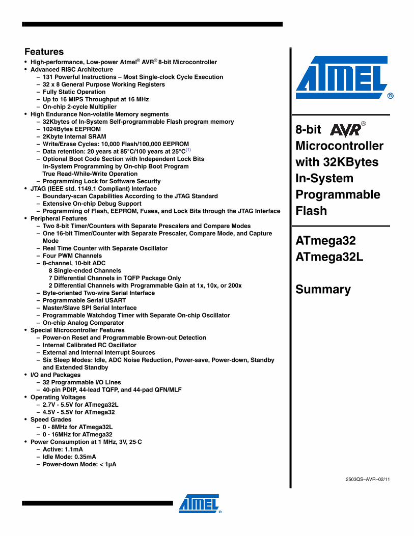
Pin Configurations
Figure 1. Pinout ATmega32
(XCK/T0) PB0(T1) PB1
(INT2/AIN0) PB2(OC0/AIN1) PB3
(SS) PB4(MOSI) PB5(MISO) PB6(SCK) PB7
RESETVCCGND
XTAL2XTAL1
(RXD) PD0(TXD) PD1(INT0) PD2(INT1) PD3
(OC1B) PD4(OC1A) PD5(ICP1) PD6
PA0 (ADC0)PA1 (ADC1)PA2 (ADC2)PA3 (ADC3)PA4 (ADC4)PA5 (ADC5)PA6 (ADC6)PA7 (ADC7)AREFGNDAVCCPC7 (TOSC2)PC6 (TOSC1)PC5 (TDI)PC4 (TDO)PC3 (TMS)PC2 (TCK)PC1 (SDA)PC0 (SCL)PD7 (OC2)
PA4 (ADC4)PA5 (ADC5)PA6 (ADC6)PA7 (ADC7)AREFGNDAVCCPC7 (TOSC2)PC6 (TOSC1)PC5 (TDI)PC4 (TDO)
(MOSI) PB5(MISO) PB6(SCK) PB7
RESETVCCGND
XTAL2XTAL1
(RXD) PD0(TXD) PD1(INT0) PD2
(INT1
) PD
3(O
C1B
) PD
4(O
C1A
) PD
5(IC
P1)
PD6
(OC
2) P
D7
VCC
GN
D(S
CL)
PC
0(S
DA)
PC
1(T
CK)
PC
2(T
MS)
PC
3
PB4
(SS)
PB3
(AIN
1/O
C0)
PB2
(AIN
0/IN
T2)
PB1
(T1)
PB0
(XC
K/T0
)G
ND
VCC
PA0
(AD
C0)
PA1
(AD
C1)
PA2
(AD
C2)
PA3
(AD
C3)
PDIP
TQFP/MLF
Note: Bottom pad shouldbe soldered to ground.
22503QS–AVR–02/11
ATmega32(L)
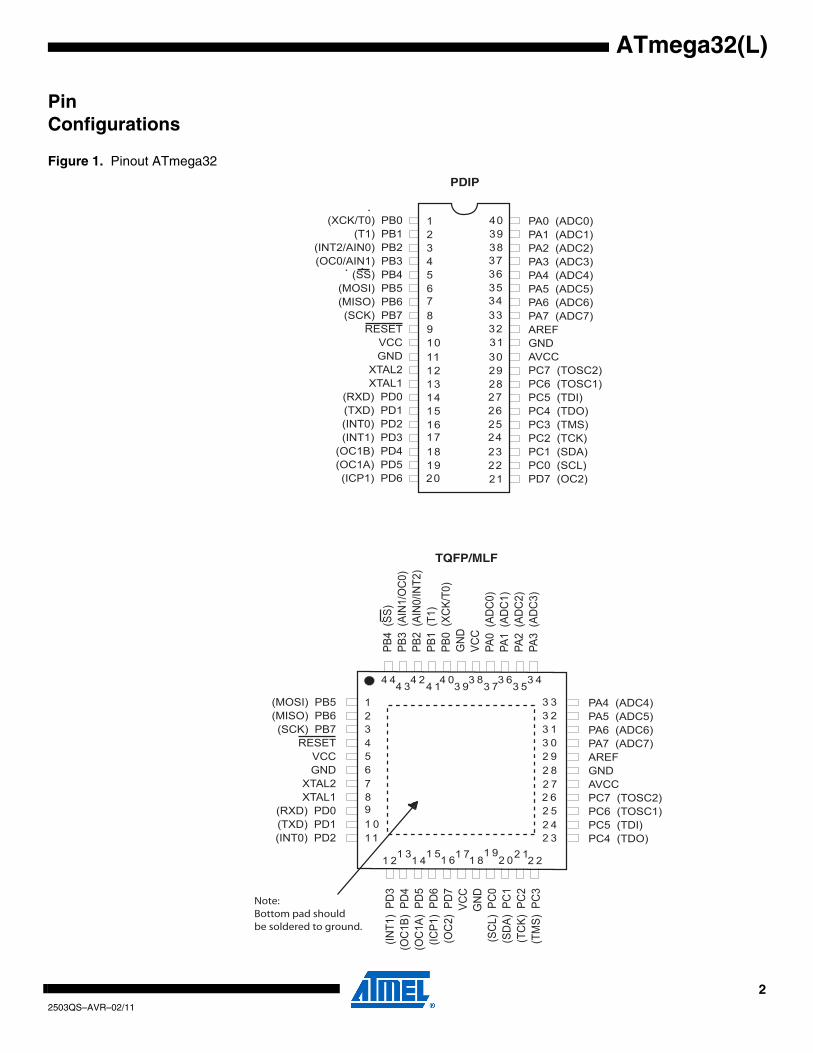
Overview The Atmel® AVR® ATmega32 is a low-power CMOS 8-bit microcontroller based on the AVRenhanced RISC architecture. By executing powerful instructions in a single clock cycle, theATmega32 achieves throughputs approaching 1 MIPS per MHz allowing the system designer tooptimize power consumption versus processing speed.
Block Diagram Figure 2. Block Diagram
INTERNALOSCILLATOR
OSCILLATOR
WATCHDOGTIMER
MCU CTRL.& TIMING
OSCILLATOR
TIMERS/COUNTERS
INTERRUPTUNIT
STACKPOINTER
EEPROM
SRAM
STATUSREGISTER
USART
PROGRAMCOUNTER
PROGRAMFLASH
INSTRUCTIONREGISTER
INSTRUCTIONDECODER
PROGRAMMINGLOGIC SPI
ADCINTERFACE
COMP.INTERFACE
PORTA DRIVERS/BUFFERS
PORTA DIGITAL INTERFACE
GENERALPURPOSE
REGISTERS
X
Y
Z
ALU
+-
PORTC DRIVERS/BUFFERS
PORTC DIGITAL INTERFACE
PORTB DIGITAL INTERFACE
PORTB DRIVERS/BUFFERS
PORTD DIGITAL INTERFACE
PORTD DRIVERS/BUFFERS
XTAL1
XTAL2
RESET
CONTROLLINES
VCC
GND
MUX &ADC
AREF
PA0 - PA7 PC0 - PC7
PD0 - PD7PB0 - PB7
AVR CPU
TWI
AVCC
INTERNALCALIBRATEDOSCILLATOR
32503QS–AVR–02/11
ATmega32(L)
The Atmel® AVR® core combines a rich instruction set with 32 general purpose working regis-ters. All the 32 registers are directly connected to the Arithmetic Logic Unit (ALU), allowing twoindependent registers to be accessed in one single instruction executed in one clock cycle. Theresulting architecture is more code efficient while achieving throughputs up to ten times fasterthan conventional CISC microcontrollers.
The ATmega32 provides the following features: 32Kbytes of In-System Programmable FlashProgram memory with Read-While-Write capabilities, 1024bytes EEPROM, 2Kbyte SRAM, 32general purpose I/O lines, 32 general purpose working registers, a JTAG interface for Boundary-scan, On-chip Debugging support and programming, three flexible Timer/Counters with com-pare modes, Internal and External Interrupts, a serial programmable USART, a byte orientedTwo-wire Serial Interface, an 8-channel, 10-bit ADC with optional differential input stage withprogrammable gain (TQFP package only), a programmable Watchdog Timer with Internal Oscil-lator, an SPI serial port, and six software selectable power saving modes. The Idle mode stopsthe CPU while allowing the USART, Two-wire interface, A/D Converter, SRAM, Timer/Counters,SPI port, and interrupt system to continue functioning. The Power-down mode saves the registercontents but freezes the Oscillator, disabling all other chip functions until the next External Inter-rupt or Hardware Reset. In Power-save mode, the Asynchronous Timer continues to run,allowing the user to maintain a timer base while the rest of the device is sleeping. The ADCNoise Reduction mode stops the CPU and all I/O modules except Asynchronous Timer andADC, to minimize switching noise during ADC conversions. In Standby mode, the crystal/reso-nator Oscillator is running while the rest of the device is sleeping. This allows very fast start-upcombined with low-power consumption. In Extended Standby mode, both the main Oscillatorand the Asynchronous Timer continue to run.
The device is manufactured using Atmel’s high density nonvolatile memory technology. The On-chip ISP Flash allows the program memory to be reprogrammed in-system through an SPI serialinterface, by a conventional nonvolatile memory programmer, or by an On-chip Boot programrunning on the AVR core. The boot program can use any interface to download the applicationprogram in the Application Flash memory. Software in the Boot Flash section will continue to runwhile the Application Flash section is updated, providing true Read-While-Write operation. Bycombining an 8-bit RISC CPU with In-System Self-Programmable Flash on a monolithic chip,the Atmel ATmega32 is a powerful microcontroller that provides a highly-flexible and cost-effec-tive solution to many embedded control applications.
The Atmel AVR ATmega32 is supported with a full suite of program and system developmenttools including: C compilers, macro assemblers, program debugger/simulators, in-circuit emula-tors, and evaluation kits.
Pin Descriptions
VCC Digital supply voltage.
GND Ground.
Port A (PA7..PA0) Port A serves as the analog inputs to the A/D Converter.
Port A also serves as an 8-bit bi-directional I/O port, if the A/D Converter is not used. Port pinscan provide internal pull-up resistors (selected for each bit). The Port A output buffers have sym-metrical drive characteristics with both high sink and source capability. When pins PA0 to PA7are used as inputs and are externally pulled low, they will source current if the internal pull-upresistors are activated. The Port A pins are tri-stated when a reset condition becomes active,even if the clock is not running.
42503QS–AVR–02/11
ATmega32(L)
Port B (PB7..PB0) Port B is an 8-bit bi-directional I/O port with internal pull-up resistors (selected for each bit). ThePort B output buffers have symmetrical drive characteristics with both high sink and sourcecapability. As inputs, Port B pins that are externally pulled low will source current if the pull-upresistors are activated. The Port B pins are tri-stated when a reset condition becomes active,even if the clock is not running.
Port B also serves the functions of various special features of the ATmega32 as listed on page57.
Port C (PC7..PC0) Port C is an 8-bit bi-directional I/O port with internal pull-up resistors (selected for each bit). ThePort C output buffers have symmetrical drive characteristics with both high sink and sourcecapability. As inputs, Port C pins that are externally pulled low will source current if the pull-upresistors are activated. The Port C pins are tri-stated when a reset condition becomes active,even if the clock is not running. If the JTAG interface is enabled, the pull-up resistors on pinsPC5(TDI), PC3(TMS) and PC2(TCK) will be activated even if a reset occurs.
The TD0 pin is tri-stated unless TAP states that shift out data are entered.
Port C also serves the functions of the JTAG interface and other special features of theATmega32 as listed on page 60.
Port D (PD7..PD0) Port D is an 8-bit bi-directional I/O port with internal pull-up resistors (selected for each bit). ThePort D output buffers have symmetrical drive characteristics with both high sink and sourcecapability. As inputs, Port D pins that are externally pulled low will source current if the pull-upresistors are activated. The Port D pins are tri-stated when a reset condition becomes active,even if the clock is not running.
Port D also serves the functions of various special features of the ATmega32 as listed on page62.
RESET Reset Input. A low level on this pin for longer than the minimum pulse length will generate areset, even if the clock is not running. The minimum pulse length is given in Table 15 on page37. Shorter pulses are not guaranteed to generate a reset.
XTAL1 Input to the inverting Oscillator amplifier and input to the internal clock operating circuit.
XTAL2 Output from the inverting Oscillator amplifier.
AVCC AVCC is the supply voltage pin for Port A and the A/D Converter. It should be externally con-nected to VCC, even if the ADC is not used. If the ADC is used, it should be connected to VCCthrough a low-pass filter.
AREF AREF is the analog reference pin for the A/D Converter.
52503QS–AVR–02/11

ATmega32(L)
Resources A comprehensive set of development tools, application notes and datasheets are available fordownload on http://www.atmel.com/avr.Note: 1.
Data Retention Reliability Qualification results show that the projected data retention failure rate is much lessthan 1 PPM over 20 years at 85°C or 100 years at 25°C.
About Code Examples
This documentation contains simple code examples that briefly show how to use various parts ofthe device. These code examples assume that the part specific header file is included beforecompilation. Be aware that not all C Compiler vendors include bit definitions in the header filesand interrupt handling in C is compiler dependent. Please confirm with the C Compiler documen-tation for more details.
62503QS–AVR–02/11
ATmega32(L)
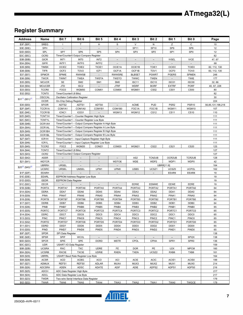
Register SummaryAddress Name Bit 7 Bit 6 Bit 5 Bit 4 Bit 3 Bit 2 Bit 1 Bit 0 Page$3F ($5F) SREG I T H S V N Z C 10$3E ($5E) SPH – – – – SP11 SP10 SP9 SP8 12$3D ($5D) SPL SP7 SP6 SP5 SP4 SP3 SP2 SP1 SP0 12$3C ($5C) OCR0 Timer/Counter0 Output Compare Register 82$3B ($5B) GICR INT1 INT0 INT2 – – – IVSEL IVCE 47, 67 $3A ($5A) GIFR INTF1 INTF0 INTF2 – – – – – 68$39 ($59) TIMSK OCIE2 TOIE2 TICIE1 OCIE1A OCIE1B TOIE1 OCIE0 TOIE0 82, 112, 130$38 ($58) TIFR OCF2 TOV2 ICF1 OCF1A OCF1B TOV1 OCF0 TOV0 83, 112, 130$37 ($57) SPMCR SPMIE RWWSB – RWWSRE BLBSET PGWRT PGERS SPMEN 248$36 ($56) TWCR TWINT TWEA TWSTA TWSTO TWWC TWEN – TWIE 177$35 ($55) MCUCR SE SM2 SM1 SM0 ISC11 ISC10 ISC01 ISC00 32, 66$34 ($54) MCUCSR JTD ISC2 – JTRF WDRF BORF EXTRF PORF 40, 67, 228$33 ($53) TCCR0 FOC0 WGM00 COM01 COM00 WGM01 CS02 CS01 CS00 80$32 ($52) TCNT0 Timer/Counter0 (8 Bits) 82
$31(1) ($51)(1) OSCCAL Oscillator Calibration Register 30OCDR On-Chip Debug Register 224
$30 ($50) SFIOR ADTS2 ADTS1 ADTS0 – ACME PUD PSR2 PSR10 56,85,131,198,218$2F ($4F) TCCR1A COM1A1 COM1A0 COM1B1 COM1B0 FOC1A FOC1B WGM11 WGM10 107$2E ($4E) TCCR1B ICNC1 ICES1 – WGM13 WGM12 CS12 CS11 CS10 110$2D ($4D) TCNT1H Timer/Counter1 – Counter Register High Byte 111$2C ($4C) TCNT1L Timer/Counter1 – Counter Register Low Byte 111$2B ($4B) OCR1AH Timer/Counter1 – Output Compare Register A High Byte 111$2A ($4A) OCR1AL Timer/Counter1 – Output Compare Register A Low Byte 111$29 ($49) OCR1BH Timer/Counter1 – Output Compare Register B High Byte 111$28 ($48) OCR1BL Timer/Counter1 – Output Compare Register B Low Byte 111$27 ($47) ICR1H Timer/Counter1 – Input Capture Register High Byte 111$26 ($46) ICR1L Timer/Counter1 – Input Capture Register Low Byte 111$25 ($45) TCCR2 FOC2 WGM20 COM21 COM20 WGM21 CS22 CS21 CS20 125$24 ($44) TCNT2 Timer/Counter2 (8 Bits) 127$23 ($43) OCR2 Timer/Counter2 Output Compare Register 127$22 ($42) ASSR – – – – AS2 TCN2UB OCR2UB TCR2UB 128$21 ($41) WDTCR – – – WDTOE WDE WDP2 WDP1 WDP0 42
$20(2) ($40)(2) UBRRH URSEL – – – UBRR[11:8] 164UCSRC URSEL UMSEL UPM1 UPM0 USBS UCSZ1 UCSZ0 UCPOL 162
$1F ($3F) EEARH – – – – – – EEAR9 EEAR8 19$1E ($3E) EEARL EEPROM Address Register Low Byte 19$1D ($3D) EEDR EEPROM Data Register 19$1C ($3C) EECR – – – – EERIE EEMWE EEWE EERE 19$1B ($3B) PORTA PORTA7 PORTA6 PORTA5 PORTA4 PORTA3 PORTA2 PORTA1 PORTA0 64$1A ($3A) DDRA DDA7 DDA6 DDA5 DDA4 DDA3 DDA2 DDA1 DDA0 64$19 ($39) PINA PINA7 PINA6 PINA5 PINA4 PINA3 PINA2 PINA1 PINA0 64$18 ($38) PORTB PORTB7 PORTB6 PORTB5 PORTB4 PORTB3 PORTB2 PORTB1 PORTB0 64$17 ($37) DDRB DDB7 DDB6 DDB5 DDB4 DDB3 DDB2 DDB1 DDB0 64$16 ($36) PINB PINB7 PINB6 PINB5 PINB4 PINB3 PINB2 PINB1 PINB0 65$15 ($35) PORTC PORTC7 PORTC6 PORTC5 PORTC4 PORTC3 PORTC2 PORTC1 PORTC0 65$14 ($34) DDRC DDC7 DDC6 DDC5 DDC4 DDC3 DDC2 DDC1 DDC0 65$13 ($33) PINC PINC7 PINC6 PINC5 PINC4 PINC3 PINC2 PINC1 PINC0 65$12 ($32) PORTD PORTD7 PORTD6 PORTD5 PORTD4 PORTD3 PORTD2 PORTD1 PORTD0 65$11 ($31) DDRD DDD7 DDD6 DDD5 DDD4 DDD3 DDD2 DDD1 DDD0 65$10 ($30) PIND PIND7 PIND6 PIND5 PIND4 PIND3 PIND2 PIND1 PIND0 65$0F ($2F) SPDR SPI Data Register 138$0E ($2E) SPSR SPIF WCOL – – – – – SPI2X 138$0D ($2D) SPCR SPIE SPE DORD MSTR CPOL CPHA SPR1 SPR0 136$0C ($2C) UDR USART I/O Data Register 159$0B ($2B) UCSRA RXC TXC UDRE FE DOR PE U2X MPCM 160$0A ($2A) UCSRB RXCIE TXCIE UDRIE RXEN TXEN UCSZ2 RXB8 TXB8 161$09 ($29) UBRRL USART Baud Rate Register Low Byte 164$08 ($28) ACSR ACD ACBG ACO ACI ACIE ACIC ACIS1 ACIS0 199$07 ($27) ADMUX REFS1 REFS0 ADLAR MUX4 MUX3 MUX2 MUX1 MUX0 214$06 ($26) ADCSRA ADEN ADSC ADATE ADIF ADIE ADPS2 ADPS1 ADPS0 216$05 ($25) ADCH ADC Data Register High Byte 217$04 ($24) ADCL ADC Data Register Low Byte 217$03 ($23) TWDR Two-wire Serial Interface Data Register 179$02 ($22) TWAR TWA6 TWA5 TWA4 TWA3 TWA2 TWA1 TWA0 TWGCE 179
72503QS–AVR–02/11
ATmega32(L)
Notes: 1. When the OCDEN Fuse is unprogrammed, the OSCCAL Register is always accessed on this address. Refer to the debug-ger specific documentation for details on how to use the OCDR Register.
2. Refer to the USART description for details on how to access UBRRH and UCSRC.3. For compatibility with future devices, reserved bits should be written to zero if accessed. Reserved I/O memory addresses
should never be written.4. Some of the Status Flags are cleared by writing a logical one to them. Note that the CBI and SBI instructions will operate on
all bits in the I/O Register, writing a one back into any flag read as set, thus clearing the flag. The CBI and SBI instructionswork with registers $00 to $1F only.
$01 ($21) TWSR TWS7 TWS6 TWS5 TWS4 TWS3 – TWPS1 TWPS0 178$00 ($20) TWBR Two-wire Serial Interface Bit Rate Register 177
Address Name Bit 7 Bit 6 Bit 5 Bit 4 Bit 3 Bit 2 Bit 1 Bit 0 Page
82503QS–AVR–02/11
ATmega32(L)
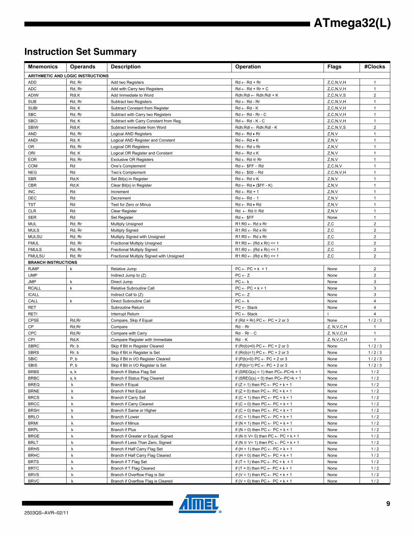
Instruction Set SummaryMnemonics Operands Description Operation Flags #ClocksARITHMETIC AND LOGIC INSTRUCTIONSADD Rd, Rr Add two Registers Rd ← Rd + Rr Z,C,N,V,H 1ADC Rd, Rr Add with Carry two Registers Rd ← Rd + Rr + C Z,C,N,V,H 1ADIW Rdl,K Add Immediate to Word Rdh:Rdl ← Rdh:Rdl + K Z,C,N,V,S 2SUB Rd, Rr Subtract two Registers Rd ← Rd - Rr Z,C,N,V,H 1SUBI Rd, K Subtract Constant from Register Rd ← Rd - K Z,C,N,V,H 1SBC Rd, Rr Subtract with Carry two Registers Rd ← Rd - Rr - C Z,C,N,V,H 1SBCI Rd, K Subtract with Carry Constant from Reg. Rd ← Rd - K - C Z,C,N,V,H 1SBIW Rdl,K Subtract Immediate from Word Rdh:Rdl ← Rdh:Rdl - K Z,C,N,V,S 2AND Rd, Rr Logical AND Registers Rd ← Rd • Rr Z,N,V 1ANDI Rd, K Logical AND Register and Constant Rd ← Rd • K Z,N,V 1OR Rd, Rr Logical OR Registers Rd ← Rd v Rr Z,N,V 1ORI Rd, K Logical OR Register and Constant Rd ← Rd v K Z,N,V 1EOR Rd, Rr Exclusive OR Registers Rd ← Rd ⊕ Rr Z,N,V 1COM Rd One’s Complement Rd ← $FF − Rd Z,C,N,V 1NEG Rd Two’s Complement Rd ← $00 − Rd Z,C,N,V,H 1SBR Rd,K Set Bit(s) in Register Rd ← Rd v K Z,N,V 1CBR Rd,K Clear Bit(s) in Register Rd ← Rd • ($FF - K) Z,N,V 1INC Rd Increment Rd ← Rd + 1 Z,N,V 1DEC Rd Decrement Rd ← Rd − 1 Z,N,V 1TST Rd Test for Zero or Minus Rd ← Rd • Rd Z,N,V 1CLR Rd Clear Register Rd ← Rd ⊕ Rd Z,N,V 1SER Rd Set Register Rd ← $FF None 1MUL Rd, Rr Multiply Unsigned R1:R0 ← Rd x Rr Z,C 2MULS Rd, Rr Multiply Signed R1:R0 ← Rd x Rr Z,C 2MULSU Rd, Rr Multiply Signed with Unsigned R1:R0 ← Rd x Rr Z,C 2FMUL Rd, Rr Fractional Multiply Unsigned R1:R0 ← (Rd x Rr) << 1 Z,C 2FMULS Rd, Rr Fractional Multiply Signed R1:R0 ← (Rd x Rr) << 1 Z,C 2FMULSU Rd, Rr Fractional Multiply Signed with Unsigned R1:R0 ← (Rd x Rr) << 1 Z,C 2BRANCH INSTRUCTIONSRJMP k Relative Jump PC ← PC + k + 1 None 2IJMP Indirect Jump to (Z) PC ← Z None 2JMP k Direct Jump PC ← k None 3RCALL k Relative Subroutine Call PC ← PC + k + 1 None 3ICALL Indirect Call to (Z) PC ← Z None 3CALL k Direct Subroutine Call PC ← k None 4RET Subroutine Return PC ← Stack None 4RETI Interrupt Return PC ← Stack I 4CPSE Rd,Rr Compare, Skip if Equal if (Rd = Rr) PC ← PC + 2 or 3 None 1 / 2 / 3CP Rd,Rr Compare Rd − Rr Z, N,V,C,H 1 CPC Rd,Rr Compare with Carry Rd − Rr − C Z, N,V,C,H 1CPI Rd,K Compare Register with Immediate Rd − K Z, N,V,C,H 1SBRC Rr, b Skip if Bit in Register Cleared if (Rr(b)=0) PC ← PC + 2 or 3 None 1 / 2 / 3SBRS Rr, b Skip if Bit in Register is Set if (Rr(b)=1) PC ← PC + 2 or 3 None 1 / 2 / 3SBIC P, b Skip if Bit in I/O Register Cleared if (P(b)=0) PC ← PC + 2 or 3 None 1 / 2 / 3SBIS P, b Skip if Bit in I/O Register is Set if (P(b)=1) PC ← PC + 2 or 3 None 1 / 2 / 3BRBS s, k Branch if Status Flag Set if (SREG(s) = 1) then PC←PC+k + 1 None 1 / 2BRBC s, k Branch if Status Flag Cleared if (SREG(s) = 0) then PC←PC+k + 1 None 1 / 2BREQ k Branch if Equal if (Z = 1) then PC ← PC + k + 1 None 1 / 2BRNE k Branch if Not Equal if (Z = 0) then PC ← PC + k + 1 None 1 / 2BRCS k Branch if Carry Set if (C = 1) then PC ← PC + k + 1 None 1 / 2BRCC k Branch if Carry Cleared if (C = 0) then PC ← PC + k + 1 None 1 / 2BRSH k Branch if Same or Higher if (C = 0) then PC ← PC + k + 1 None 1 / 2BRLO k Branch if Lower if (C = 1) then PC ← PC + k + 1 None 1 / 2BRMI k Branch if Minus if (N = 1) then PC ← PC + k + 1 None 1 / 2BRPL k Branch if Plus if (N = 0) then PC ← PC + k + 1 None 1 / 2BRGE k Branch if Greater or Equal, Signed if (N ⊕ V= 0) then PC ← PC + k + 1 None 1 / 2BRLT k Branch if Less Than Zero, Signed if (N ⊕ V= 1) then PC ← PC + k + 1 None 1 / 2BRHS k Branch if Half Carry Flag Set if (H = 1) then PC ← PC + k + 1 None 1 / 2BRHC k Branch if Half Carry Flag Cleared if (H = 0) then PC ← PC + k + 1 None 1 / 2BRTS k Branch if T Flag Set if (T = 1) then PC ← PC + k + 1 None 1 / 2BRTC k Branch if T Flag Cleared if (T = 0) then PC ← PC + k + 1 None 1 / 2BRVS k Branch if Overflow Flag is Set if (V = 1) then PC ← PC + k + 1 None 1 / 2BRVC k Branch if Overflow Flag is Cleared if (V = 0) then PC ← PC + k + 1 None 1 / 2
92503QS–AVR–02/11

ATmega32(L)
BRIE k Branch if Interrupt Enabled if ( I = 1) then PC ← PC + k + 1 None 1 / 2BRID k Branch if Interrupt Disabled if ( I = 0) then PC ← PC + k + 1 None 1 / 2DATA TRANSFER INSTRUCTIONSMOV Rd, Rr Move Between Registers Rd ← Rr None 1MOVW Rd, Rr Copy Register Word Rd+1:Rd ← Rr+1:Rr None 1LDI Rd, K Load Immediate Rd ← K None 1LD Rd, X Load Indirect Rd ← (X) None 2LD Rd, X+ Load Indirect and Post-Inc. Rd ← (X), X ← X + 1 None 2LD Rd, - X Load Indirect and Pre-Dec. X ← X - 1, Rd ← (X) None 2LD Rd, Y Load Indirect Rd ← (Y) None 2LD Rd, Y+ Load Indirect and Post-Inc. Rd ← (Y), Y ← Y + 1 None 2LD Rd, - Y Load Indirect and Pre-Dec. Y ← Y - 1, Rd ← (Y) None 2LDD Rd,Y+q Load Indirect with Displacement Rd ← (Y + q) None 2LD Rd, Z Load Indirect Rd ← (Z) None 2LD Rd, Z+ Load Indirect and Post-Inc. Rd ← (Z), Z ← Z+1 None 2LD Rd, -Z Load Indirect and Pre-Dec. Z ← Z - 1, Rd ← (Z) None 2LDD Rd, Z+q Load Indirect with Displacement Rd ← (Z + q) None 2LDS Rd, k Load Direct from SRAM Rd ← (k) None 2ST X, Rr Store Indirect (X) ← Rr None 2ST X+, Rr Store Indirect and Post-Inc. (X) ← Rr, X ← X + 1 None 2ST - X, Rr Store Indirect and Pre-Dec. X ← X - 1, (X) ← Rr None 2ST Y, Rr Store Indirect (Y) ← Rr None 2ST Y+, Rr Store Indirect and Post-Inc. (Y) ← Rr, Y ← Y + 1 None 2ST - Y, Rr Store Indirect and Pre-Dec. Y ← Y - 1, (Y) ← Rr None 2STD Y+q,Rr Store Indirect with Displacement (Y + q) ← Rr None 2ST Z, Rr Store Indirect (Z) ← Rr None 2ST Z+, Rr Store Indirect and Post-Inc. (Z) ← Rr, Z ← Z + 1 None 2ST -Z, Rr Store Indirect and Pre-Dec. Z ← Z - 1, (Z) ← Rr None 2STD Z+q,Rr Store Indirect with Displacement (Z + q) ← Rr None 2STS k, Rr Store Direct to SRAM (k) ← Rr None 2LPM Load Program Memory R0 ← (Z) None 3LPM Rd, Z Load Program Memory Rd ← (Z) None 3LPM Rd, Z+ Load Program Memory and Post-Inc Rd ← (Z), Z ← Z+1 None 3SPM Store Program Memory (Z) ← R1:R0 None -IN Rd, P In Port Rd ← P None 1OUT P, Rr Out Port P ← Rr None 1PUSH Rr Push Register on Stack Stack ← Rr None 2POP Rd Pop Register from Stack Rd ← Stack None 2BIT AND BIT-TEST INSTRUCTIONSSBI P,b Set Bit in I/O Register I/O(P,b) ← 1 None 2CBI P,b Clear Bit in I/O Register I/O(P,b) ← 0 None 2LSL Rd Logical Shift Left Rd(n+1) ← Rd(n), Rd(0) ← 0 Z,C,N,V 1LSR Rd Logical Shift Right Rd(n) ← Rd(n+1), Rd(7) ← 0 Z,C,N,V 1ROL Rd Rotate Left Through Carry Rd(0)←C,Rd(n+1)← Rd(n),C←Rd(7) Z,C,N,V 1ROR Rd Rotate Right Through Carry Rd(7)←C,Rd(n)← Rd(n+1),C←Rd(0) Z,C,N,V 1ASR Rd Arithmetic Shift Right Rd(n) ← Rd(n+1), n=0..6 Z,C,N,V 1SWAP Rd Swap Nibbles Rd(3..0)←Rd(7..4),Rd(7..4)←Rd(3..0) None 1BSET s Flag Set SREG(s) ← 1 SREG(s) 1BCLR s Flag Clear SREG(s) ← 0 SREG(s) 1BST Rr, b Bit Store from Register to T T ← Rr(b) T 1BLD Rd, b Bit load from T to Register Rd(b) ← T None 1SEC Set Carry C ← 1 C 1CLC Clear Carry C ← 0 C 1SEN Set Negative Flag N ← 1 N 1CLN Clear Negative Flag N ← 0 N 1SEZ Set Zero Flag Z ← 1 Z 1CLZ Clear Zero Flag Z ← 0 Z 1SEI Global Interrupt Enable I ← 1 I 1CLI Global Interrupt Disable I ← 0 I 1SES Set Signed Test Flag S ← 1 S 1CLS Clear Signed Test Flag S ← 0 S 1SEV Set Twos Complement Overflow. V ← 1 V 1CLV Clear Twos Complement Overflow V ← 0 V 1SET Set T in SREG T ← 1 T 1CLT Clear T in SREG T ← 0 T 1SEH Set Half Carry Flag in SREG H ← 1 H 1
Mnemonics Operands Description Operation Flags #Clocks
102503QS–AVR–02/11
ATmega32(L)
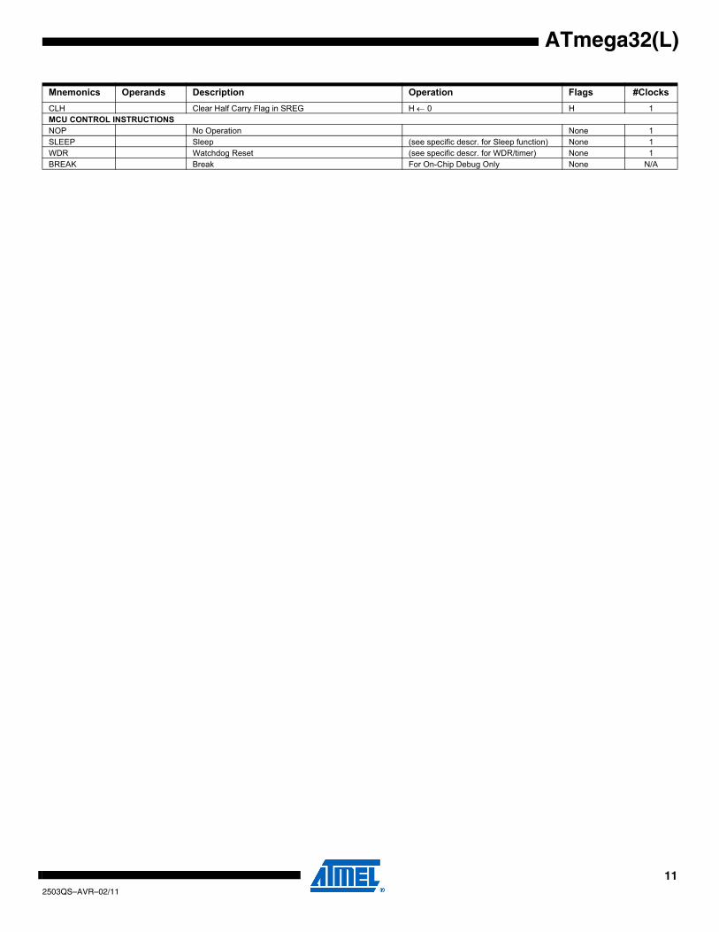
CLH Clear Half Carry Flag in SREG H ← 0 H 1MCU CONTROL INSTRUCTIONSNOP No Operation None 1SLEEP Sleep (see specific descr. for Sleep function) None 1WDR Watchdog Reset (see specific descr. for WDR/timer) None 1BREAK Break For On-Chip Debug Only None N/A
Mnemonics Operands Description Operation Flags #Clocks
112503QS–AVR–02/11
ATmega32(L)
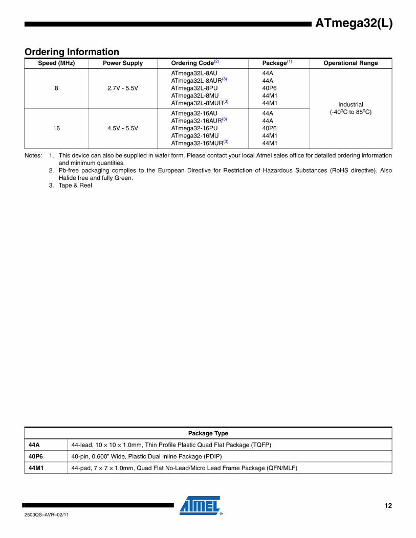
Ordering Information
Notes: 1. This device can also be supplied in wafer form. Please contact your local Atmel sales office for detailed ordering informationand minimum quantities.
2. Pb-free packaging complies to the European Directive for Restriction of Hazardous Substances (RoHS directive). AlsoHalide free and fully Green.
3. Tape & Reel
Speed (MHz) Power Supply Ordering Code(2) Package(1) Operational Range
8 2.7V - 5.5V
ATmega32L-8AUATmega32L-8AUR(3)
ATmega32L-8PUATmega32L-8MUATmega32L-8MUR(3)
44A44A40P644M144M1 Industrial
(-40oC to 85oC)
16 4.5V - 5.5V
ATmega32-16AUATmega32-16AUR(3)
ATmega32-16PUATmega32-16MUATmega32-16MUR(3)
44A44A40P644M144M1
Package Type
44A 44-lead, 10 × 10 × 1.0mm, Thin Profile Plastic Quad Flat Package (TQFP)
40P6 40-pin, 0.600” Wide, Plastic Dual Inline Package (PDIP)
44M1 44-pad, 7 × 7 × 1.0mm, Quad Flat No-Lead/Micro Lead Frame Package (QFN/MLF)
122503QS–AVR–02/11
ATmega32(L)
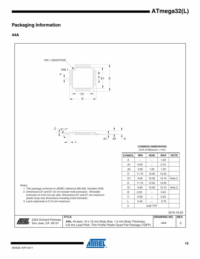
Packaging Information
44A
2325 Orchard Parkway San Jose, CA 95131
TITLE DRAWING NO.
R
REV.
44A, 44-lead, 10 x 10 mm Body Size, 1.0 mm Body Thickness,0.8 mm Lead Pitch, Thin Profile Plastic Quad Flat Package (TQFP)
C44A
2010-10-20
PIN 1 IDENTIFIER
0°~7°
PIN 1
L
C
A1 A2 A
D1
D
e
E1 E
B
COMMON DIMENSIONS(Unit of Measure = mm)
SYMBOL MIN NOM MAX NOTE
Notes: 1. This package conforms to JEDEC reference MS-026, Variation ACB. 2. Dimensions D1 and E1 do not include mold protrusion. Allowable protrusion is 0.25 mm per side. Dimensions D1 and E1 are maximum plastic body size dimensions including mold mismatch. 3. Lead coplanarity is 0.10 mm maximum.
A – – 1.20
A1 0.05 – 0.15
A2 0.95 1.00 1.05
D 11.75 12.00 12.25
D1 9.90 10.00 10.10 Note 2
E 11.75 12.00 12.25
E1 9.90 10.00 10.10 Note 2
B 0.30 – 0.45
C 0.09 – 0.20
L 0.45 – 0.75
e 0.80 TYP
132503QS–AVR–02/11
ATmega32(L)
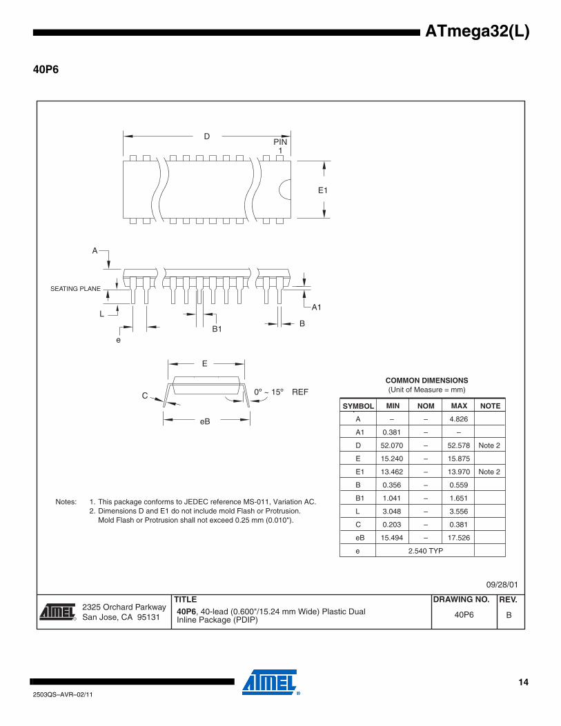
40P6
2325 Orchard Parkway San Jose, CA 95131
TITLE DRAWING NO.
R
REV. 40P6, 40-lead (0.600"/15.24 mm Wide) Plastic Dual Inline Package (PDIP) B40P6
09/28/01
PIN1
E1
A1
B
REF
E
B1
C
L
SEATING PLANE
A
0º ~ 15º
D
e
eB
COMMON DIMENSIONS(Unit of Measure = mm)
SYMBOL MIN NOM MAX NOTE
A – – 4.826
A1 0.381 – –
D 52.070 – 52.578 Note 2
E 15.240 – 15.875
E1 13.462 – 13.970 Note 2
B 0.356 – 0.559
B1 1.041 – 1.651
L 3.048 – 3.556
C 0.203 – 0.381
eB 15.494 – 17.526
e 2.540 TYP
Notes: 1. This package conforms to JEDEC reference MS-011, Variation AC. 2. Dimensions D and E1 do not include mold Flash or Protrusion.
Mold Flash or Protrusion shall not exceed 0.25 mm (0.010").
142503QS–AVR–02/11
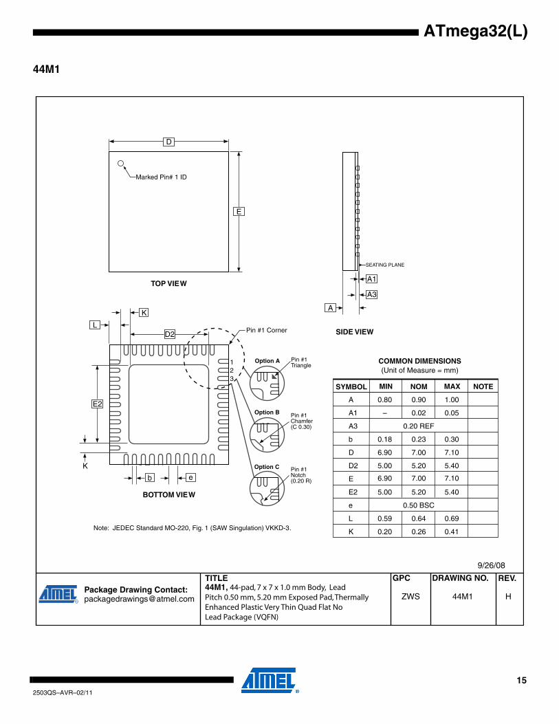
ATmega32(L)
44M1
TITLE DRAWING NO.GPC REV. Package Drawing Contact: [email protected] 44M1ZWS H
44M1, 44-pad, 7 x 7 x 1.0 mm Body, Lead Pitch 0.50 mm, 5.20 mm Exposed Pad, Thermally Enhanced Plastic Very Thin Quad Flat No Lead Package (VQFN)
9/26/08
COMMON DIMENSIONS(Unit of Measure = mm)
SYMBOL MIN NOM MAX NOTE
A 0.80 0.90 1.00
A1 – 0.02 0.05
A3 0.20 REF
b 0.18 0.23 0.30
D
D2 5.00 5.20 5.40
6.90 7.00 7.10
6.90 7.00 7.10
E
E2 5.00 5.20 5.40
e 0.50 BSC
L 0.59 0.64 0.69
K 0.20 0.26 0.41Note: JEDEC Standard MO-220, Fig. 1 (SAW Singulation) VKKD-3.
TOP VIEW
SIDE VIEW
BOTTOM VIEW
D
E
Marked Pin# 1 ID
E2
D2
b e
Pin #1 CornerL
A1
A3
A
SEATING PLANE
Pin #1 Triangle
Pin #1 Chamfer(C 0.30)
Option A
Option B
Pin #1 Notch(0.20 R)
Option C
K
K
123
152503QS–AVR–02/11
ATmega32(L)
Errata
ATmega32, rev. A to F
• First Analog Comparator conversion may be delayed• Interrupts may be lost when writing the timer registers in the asynchronous timer• IDCODE masks data from TDI input• Reading EEPROM by using ST or STS to set EERE bit triggers unexpected interrupt request.
1. First Analog Comparator conversion may be delayed
If the device is powered by a slow rising VCC, the first Analog Comparator conversion willtake longer than expected on some devices.
Problem Fix/Workaround
When the device has been powered or reset, disable then enable theAnalog Comparatorbefore the first conversion.
2. Interrupts may be lost when writing the timer registers in the asynchronous timer
The interrupt will be lost if a timer register that is synchronous timer clock is written when theasynchronous Timer/Counter register (TCNTx) is 0x00.
Problem Fix/Workaround
Always check that the asynchronous Timer/Counter register neither have the value 0xFF nor0x00 before writing to the asynchronous Timer Control Register (TCCRx), asynchronous-Timer Counter Register (TCNTx), or asynchronous Output Compare Register (OCRx).
3. IDCODE masks data from TDI input
The JTAG instruction IDCODE is not working correctly. Data to succeeding devices arereplaced by all-ones during Update-DR.
Problem Fix / Workaround
– If ATmega32 is the only device in the scan chain, the problem is not visible.
– Select the Device ID Register of the ATmega32 by issuing the IDCODE instruction orby entering the Test-Logic-Reset state of the TAP controller to read out the contentsof its Device ID Register and possibly data from succeeding devices of the scanchain. Issue the BYPASS instruction to the ATmega32 while reading the Device IDRegisters of preceding devices of the boundary scan chain.
– If the Device IDs of all devices in the boundary scan chain must be capturedsimultaneously, the ATmega32 must be the fist device in the chain.
4. Reading EEPROM by using ST or STS to set EERE bit triggers unexpected interruptrequest.
Reading EEPROM by using the ST or STS command to set the EERE bit in the EECR reg-ister triggers an unexpected EEPROM interrupt request.
Problem Fix / Workaround
Always use OUT or SBI to set EERE in EECR.
162503QS–AVR–02/11
ATmega32(L)
Datasheet Revision History
Please note that the referring page numbers in this section are referred to this document. Thereferring revision in this section are referring to the document revision.
Changes from Rev. 2503P-07/09 to Rev. 2503Q-02/11
1. Updated “Packaging Information” on page 333, by replacing the package 44A by acorrect one.
2. Updated the datasheet according to the Atmel new Brand Style Guide.
3. Updated “Ordering Information” on page 332 to include Tape & Reel devices.
Changes from Rev. 2503O-07/09 to Rev. 2503P-07/10
1. Inserted Note in “Performing Page Erase by SPM” on page 251.
2. Note 6 and Note 7 in Table 119 on page 290 have been removed.
3. Updated “Performing Page Erase by SPM” on page 251.
Changes from Rev. 2503N-06/08 to Rev.2503O-07/09
1. Updated “Errata” on page 336 .
2. Updated the TOC with new template (version 5.10)
Changes from Rev. 2503M-05/08 to Rev.2503N-06/08
1. Added the note “Not recommended for new designs” on “Features” on page 1.
Changes from Rev. 2503L-05/08 to Rev.2503M-05/08
1. Updated “Ordering Information” on page 12:
- Commercial ordering codes removed.
- Non Pb-free package option removed.
2. Removed note from Feature list in “Analog to Digital Converter” on page 201.
3. Removed note from Table 84 on page 215.
Changes from Rev. 2503K-08/07 to Rev.2503L-05/08
1. Updated “Fast PWM Mode” on page 75 in “8-bit Timer/Counter0 with PWM” on page69:
– Removed the last section describing how to achieve a frequency with 50% duty cycle waveform output in fast PWM mode.
Changes from Rev. 2503J-10/06 to Rev.2503K-08/07
1. Renamed “Input Capture Trigger Source” to “Input Capture Pin Source” on page 94.
2. Updated “Features” on page 1.
3. Added “Data Retention” on page 6.
4. Updated “Errata” on page 336.
172503QS–AVR–02/11
ATmega32(L)
5. Updated “Slave Mode” on page 136.
Changes from Rev. 2503I-04/06 to Rev.2503J-10/06
1. Updated “Fast PWM Mode” on page 99.
2. Updated Table 38 on page 80, Table 40 on page 81, Table 45 on page 108, Table 47 onpage 109, Table 50 on page 125 and Table 52 on page 126.
3. Updated typo in table note 6 in “DC Characteristics” on page 287.
4. Updated “Errata” on page 336.
Changes from Rev. 2503H-03/05 to Rev. 2503I-04/06
1. Updated Figure 1 on page 2.
2. Added “Resources” on page 6.
3. Added note to “Timer/Counter Oscillator” on page 31.
4. Updated “Serial Peripheral Interface – SPI” on page 132.
5. Updated note in “Bit Rate Generator Unit” on page 175.
6. Updated Table 86 on page 218.
7. Updated “DC Characteristics” on page 287.
Changes from Rev. 2503G-11/04 to Rev. 2503H-03/05
1. MLF-package alternative changed to “Quad Flat No-Lead/Micro Lead Frame PackageQFN/MLF”.
2. Updated “Electrical Characteristics” on page 287
3. Updated “Ordering Information” on page 332.
Changes from Rev. 2503F-12/03 to Rev. 2503G-11/04
1. “Channel” renamed “Compare unit” in Timer/Counter sections, ICP renamed ICP1.
2. Updated Table 7 on page 29, Table 15 on page 37, Table 81 on page 206, Table 114 onpage 272, Table 115 on page 273, and Table 118 on page 289.
3. Updated Figure 1 on page 2, Figure 46 on page 100.
4. Updated “Version” on page 226.
5. Updated “Calibration Byte” on page 258.
6. Added section “Page Size” on page 258.
7. Updated “ATmega32 Typical Characteristics” on page 296.
8. Updated “Ordering Information” on page 332.
Changes from Rev. 2503E-09/03 to Rev. 2503F-12/03
1. Updated “Calibrated Internal RC Oscillator” on page 29.
182503QS–AVR–02/11
ATmega32(L)
Changes from Rev. 2503D-02/03 to Rev. 2503E-09/03
1. Updated and changed “On-chip Debug System” to “JTAG Interface and On-chipDebug System” on page 35.
2. Updated Table 15 on page 37.
3. Updated “Test Access Port – TAP” on page 219 regarding the JTAGEN fuse.
4. Updated description for Bit 7 – JTD: JTAG Interface Disable on page 228.
5. Added a note regarding JTAGEN fuse to Table 104 on page 257.
6. Updated Absolute Maximum Ratings* , DC Characteristics and ADC Characteristics in“Electrical Characteristics” on page 287.
7. Added a proposal for solving problems regarding the JTAG instruction IDCODE in“Errata” on page 336.
Changes from Rev. 2503C-10/02 to Rev. 2503D-02/03
1. Added EEAR9 in EEARH in “Register Summary” on page 327.
2. Added Chip Erase as a first step in“Programming the Flash” on page 284 and “Pro-gramming the EEPROM” on page 285.
3. Removed reference to “Multi-purpose Oscillator” application note and “32 kHz Crys-tal Oscillator” application note, which do not exist.
4. Added information about PWM symmetry for Timer0 and Timer2.
5. Added note in “Filling the Temporary Buffer (Page Loading)” on page 251 about writ-ing to the EEPROM during an SPM Page Load.
6. Added “Power Consumption” data in “Features” on page 1.
7. Added section “EEPROM Write During Power-down Sleep Mode” on page 22.
8. Added note about Differential Mode with Auto Triggering in “Prescaling and Conver-sion Timing” on page 204.
9. Updated Table 89 on page 232.
10.Added updated “Packaging Information” on page 333.
Changes from Rev. 2503B-10/02 to Rev. 2503C-10/02
1. Updated the “DC Characteristics” on page 287.
Changes from Rev. 2503A-03/02 to Rev. 2503B-10/02
1. Canged the endurance on the Flash to 10,000 Write/Erase Cycles.
2. Bit nr.4 – ADHSM – in SFIOR Register removed.
3. Added the section “Default Clock Source” on page 25.
4. When using External Clock there are some limitations regards to change of fre-quency. This is described in “External Clock” on page 31 and Table 117 on page 289.
192503QS–AVR–02/11
ATmega32(L)
5. Added a sub section regarding OCD-system and power consumption in the section“Minimizing Power Consumption” on page 34.
6. Corrected typo (WGM-bit setting) for:– “Fast PWM Mode” on page 75 (Timer/Counter0)– “Phase Correct PWM Mode” on page 76 (Timer/Counter0)– “Fast PWM Mode” on page 120 (Timer/Counter2)– “Phase Correct PWM Mode” on page 121 (Timer/Counter2)
7. Corrected Table 67 on page 164 (USART).
8. Updated VIL, IIL, and IIH parameter in “DC Characteristics” on page 287.
9. Updated Description of OSCCAL Calibration Byte.
In the datasheet, it was not explained how to take advantage of the calibration bytes for 2, 4,and 8 MHz Oscillator selections. This is now added in the following sections:
Improved description of “Oscillator Calibration Register – OSCCAL” on page 30 and “Cali-bration Byte” on page 258.
10. Corrected typo in Table 42.
11. Corrected description in Table 45 and Table 46.
12. Updated Table 118, Table 120, and Table 121.
13. Added “Errata” on page 336.
202503QS–AVR–02/11
Atmel Corporation2325 Orchard ParkwaySan Jose, CA 95131USATel: (+1)(408) 441-0311Fax: (+1)(408) 487-2600 www.atmel.com
Atmel Asia LimitedUnit 1-5 & 16, 19/FBEA Tower, Millennium City 5418 Kwun Tong RoadKwun Tong, KowloonHONG KONGTel: (+852) 2245-6100Fax: (+852) 2722-1369
Atmel Munich GmbHBusiness CampusParkring 4D-85748 Garching b. MunichGERMANYTel: (+49) 89-31970-0Fax: (+49) 89-3194621
Atmel Japan9F, Tonetsu Shinkawa Bldg.1-24-8 ShinkawaChuo-ku, Tokyo 104-0033JAPANTel: (+81)(3) 3523-3551Fax: (+81)(3) 3523-7581
© 2011 Atmel Corporation. All rights reserved. / Rev. CORP0XXXX
Atmel®, Atmel logo and combinations thereof, AVR® and others are registered trademarks or trademarks of Atmel Corporation or its subsidiaries. Other terms and product names may be trademarks of others.
Disclaimer: The information in this document is provided in connection with Atmel products. No license, express or implied, by estoppel or otherwise, to any intellectual property right is granted by this document or in connection with the sale of Atmel products. EXCEPT AS SET FORTH IN THE ATMEL TERMS AND CONDITIONS OF SALES LOCATED ON THE ATMEL WEBSITE, ATMEL ASSUMES NO LIABILITY WHATSOEVER AND DISCLAIMS ANY EXPRESS, IMPLIED OR STATUTORY WARRANTY RELATING TO ITS PRODUCTS INCLUDING, BUT NOT LIMITED TO, THE IMPLIED WARRANTY OF MERCHANTABILITY, FITNESS FOR A PARTICULAR PURPOSE, OR NON-INFRINGEMENT. IN NO EVENT SHALL ATMEL BE LIABLE FOR ANY DIRECT, INDIRECT, CONSEQUENTIAL, PUNITIVE, SPECIAL OR INCIDENTAL DAMAGES (INCLUDING, WITHOUT LIMITATION, DAMAGES FOR LOSS AND PROF-ITS, BUSINESS INTERRUPTION, OR LOSS OF INFORMATION) ARISING OUT OF THE USE OR INABILITY TO USE THIS DOCUMENT, EVEN IF ATMEL HAS BEEN ADVISED OF THE POSSIBILITY OF SUCH DAMAGES. Atmel makes no representations or warranties with respect to the accuracy or com-pleteness of the contents of this document and reserves the right to make changes to specifications and product descriptions at any time without notice. Atmel does not make any commitment to update the information contained herein. Unless specifically provided otherwise, Atmel products are not suit-able for, and shall not be used in, automotive applications. Atmel products are not intended, authorized, or warranted for use as components in applica-tions intended to support or sustain life.
2503QS–AVR–02/11
![Atmel ATSHA204 - SparkFun Electronicscdn.sparkfun.com/.../Atmel-8740-CryptoAuth-ATSHA204-Datasheet.pdf · Atmel ATSHA204 [DATASHEET] 5 Atmel–8740E–CryptoAuth–ATSHA204–Datasheet–022013](https://img.pdfslide.us/doc/110x75/5e25fe64d9a5567efa4c5ccc/atmel-atsha204-sparkfun-atmel-atsha204-datasheet-5-atmela8740eacryptoauthaatsha204adatasheeta022013.jpg)
![Atmel ATmega16U4, ATmega32U4 Datasheet Summaryww1.microchip.com/.../Atmel-7766-8-bit-AVR-ATmega16U4-32U4_Sum… · DATASHEET SUMMARY. ATmega16U4/32U4 [DATASHEET] ... The AVR core](https://img.pdfslide.us/doc/110x75/5aeada877f8b9a66258c91a3/atmel-atmega16u4-atmega32u4-datasheet-datasheet-summary-atmega16u432u4-datasheet.jpg)
![Atmel MSL2021 Datasheet - Microchip Technologyww1.microchip.com/.../Atmel-4062-LED-driver-MSL2021_datasheet.pdf · MSL2021 [DATASHEET] 2 42062A–LED–02/2013 1. Introduction](https://img.pdfslide.us/doc/110x75/5bcb74ae09d3f2d30a8c0ea6/atmel-msl2021-datasheet-microchip-msl2021-datasheet-2-42062aled022013.jpg)
![Atmel | SMART SAM9G15 Datasheet - Microchip Technologyww1.microchip.com/downloads/en/DeviceDoc/Atmel-11052-32-bit-ARM926EJ-S... · SAM9G15 [DATASHEET] Atmel-11052G-ATARM-SAM9G15-Datasheet_31-Aug-15](https://img.pdfslide.us/doc/110x75/5fc5b8513d95c47bda5a5ac4/atmel-smart-sam9g15-datasheet-microchip-sam9g15-datasheet-atmel-11052g-atarm-sam9g15-datasheet31-aug-15.jpg)
![AT88SC0808CA - ww1.microchip.com · AT88SC0808CA [Summary DATASHEET] Atmel-5204IS-CryptoMem-AT88SC0808CA-Datasheet-Summary_072015 3 1. Description The Atmel AT88SC0808CA member of](https://img.pdfslide.us/doc/110x75/60c1dccabc7457567f20c71c/at88sc0808ca-ww1-at88sc0808ca-summary-datasheet-atmel-5204is-cryptomem-at88sc0808ca-datasheet-summary072015.jpg)


![Atmel ATmega16U4, ATmega32U4 Datasheet …...ATmega16U4/32U4 [DATASHEET] 8](https://img.pdfslide.us/doc/110x75/5f0a39897e708231d42a9d86/-atmel-atmega16u4-atmega32u4-datasheet-atmega16u432u4-datasheet-8.jpg)
![Atmel 9372 Smart Rf Ata8520 Datasheet[1]](https://img.pdfslide.us/doc/110x75/577c79811a28abe05492eaf4/atmel-9372-smart-rf-ata8520-datasheet1.jpg)