Embed Size (px)
Citation preview
Atlas OW, Praha, September 16, 2003 Vaclav Vrba, Institute of Physics, AS CR 1
Vaclav Vrba
Institute of Physics, AS CR, Prague
Pixel Detector Status
Atlas OW, Praha, September 16, 2003 Vaclav Vrba, Institute of Physics, AS CR 2
• Mechanics and services
• System tests
• Rad-hard electronics
• Module production
• Sensors
• Schedule
Layout of the talk
Atlas OW, Praha, September 16, 2003 Vaclav Vrba, Institute of Physics, AS CR 3
Mechanics and servicesMechanics and services
Forward A
Forward C
Barrel
PST FlangesPP1 End Plug
A 7m long object
A 7m long object
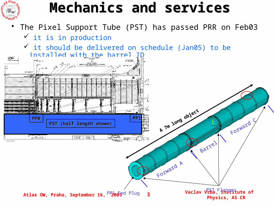
The Pixel Support Tube (PST) has passed PRR on Feb03 it is in production it should be delivered on schedule (Jan05) to be installed with the
barrel ID
PST (half length shown)PST (half length shown)PP0PP0 PP1PP1
Atlas OW, Praha, September 16, 2003 Vaclav Vrba, Institute of Physics, AS CR 4
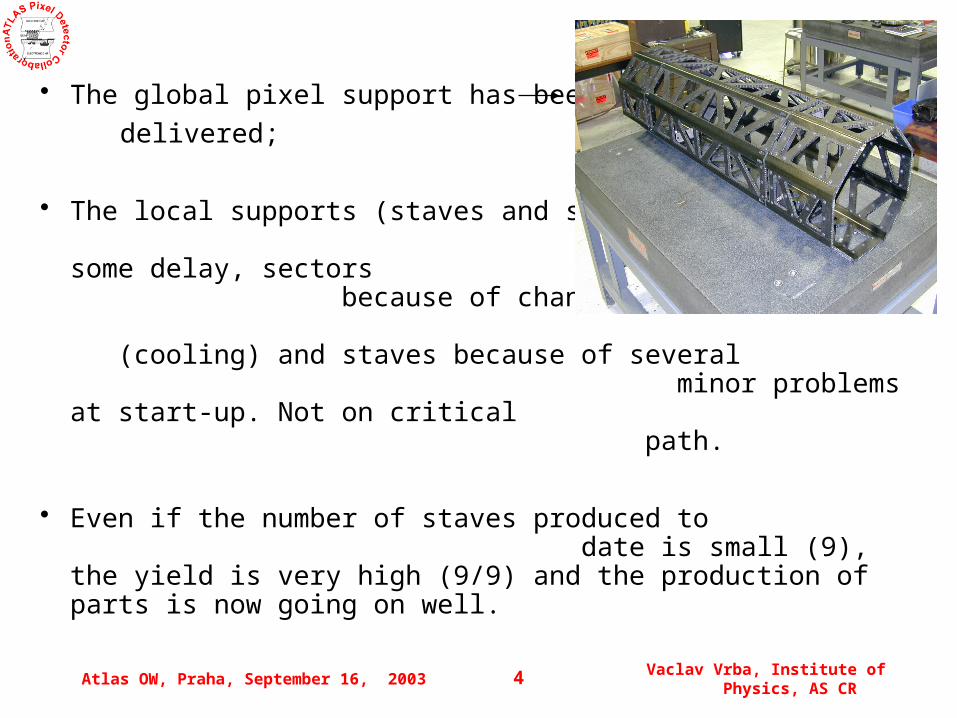
The global pixel support has been
delivered;
The local supports (staves and sectors) have accumulated some delay, sectors because of change in pressure specs (cooling) and staves because of several minor problems at start-up. Not on critical path.
Even if the number of staves produced to date is small (9), the yield is very high (9/9) and the production of parts is now going on well.
Atlas OW, Praha, September 16, 2003 Vaclav Vrba, Institute of Physics, AS CR 5
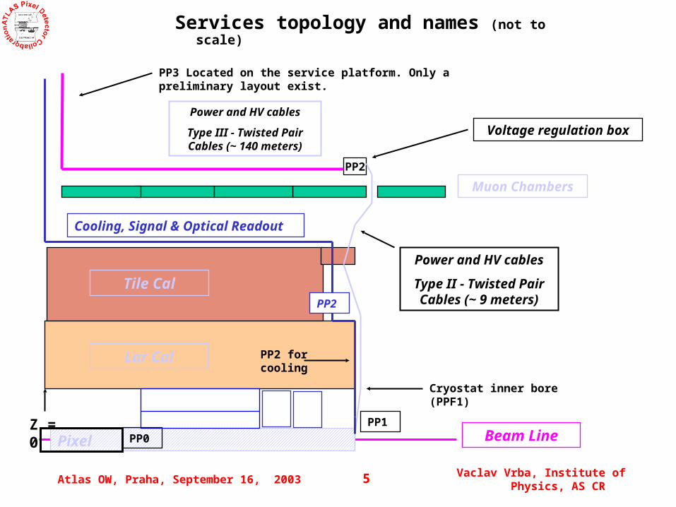
Services topology and names (not to scale)
Pixel PP1
PP2
PP3 Located on the service platform. Only a preliminary layout exist.
Tile Cal
Lar Cal
Beam Line
Muon Chambers
Cooling, Signal & Optical Readout
Power and HV cables
Type II - Twisted Pair Cables (~ 9 meters)
Cryostat inner bore (PPF1)
Power and HV cables
Type III - Twisted Pair Cables (~ 140 meters)
PP2
PP2 for cooling
Z = 0
Voltage regulation box
PP0
Atlas OW, Praha, September 16, 2003 Vaclav Vrba, Institute of Physics, AS CR 6
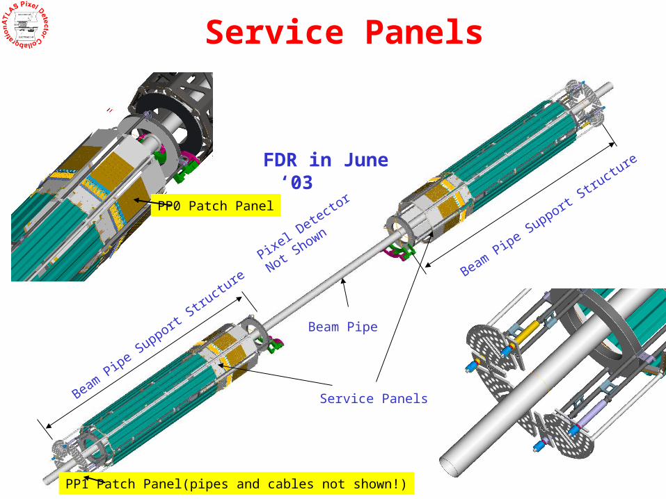
Service Panels
FDR in June ‘03
Beam Pipe Support Stru
cture
Beam Pipe Support Stru
cture
Pixel Detecto
r
Not Shown
Beam Pipe
Service Panels
PP1 Patch Panel(pipes and cables not shown!)
PP0 Patch Panel
Atlas OW, Praha, September 16, 2003 Vaclav Vrba, Institute of Physics, AS CR 7
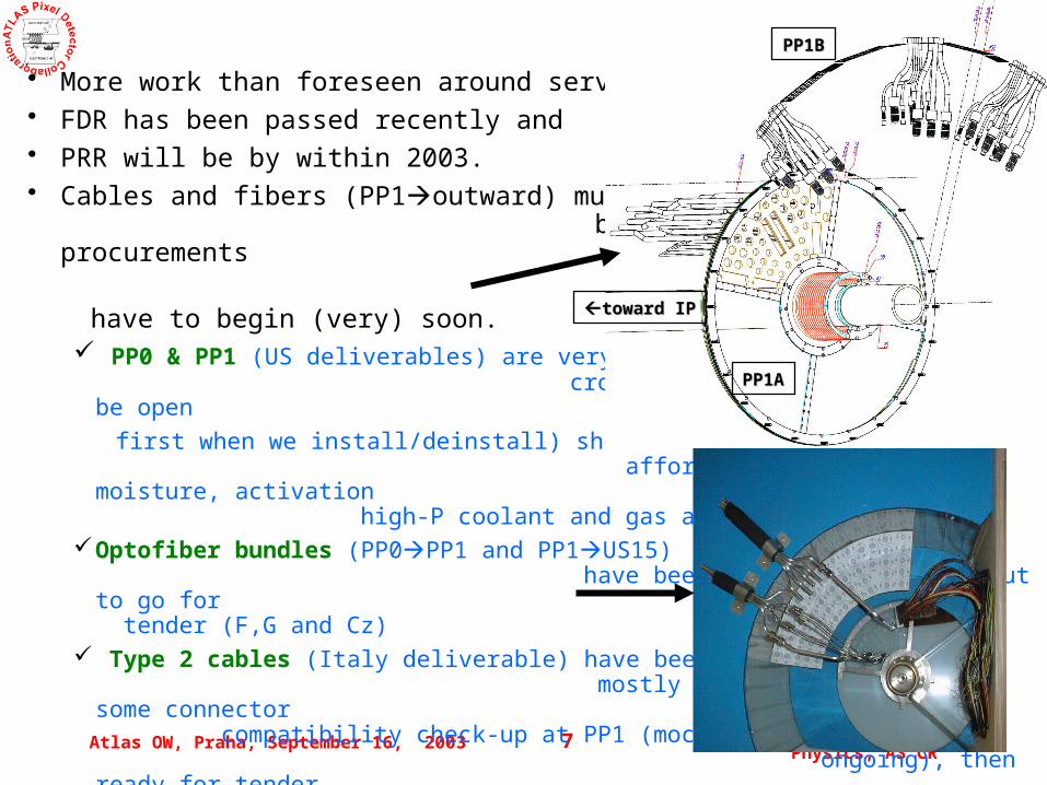
More work than foreseen around services, FDR has been passed recently and PRR will be by within 2003. Cables and fibers (PP1outward) must
be installed in Fall 04, so procurements
have to begin (very) soon. PP0 & PP1 (US deliverables) are very
crowded and PP1 (the interface to be open
first when we install/deinstall) should also afford issues related to moisture, activation high-P coolant and gas and electrical seals.
Optofiber bundles (PP0PP1 and PP1US15) have been designed and are about to go for tender (F,G and Cz)
Type 2 cables (Italy deliverable) have been mostly defined, still missing some connector compatibility check-up at PP1 (mock-up ongoing), then ready for tender
Type 3 cables (F, G, I, and US) mostly defined,
Work in progress…
PP1APP1A
PP1BPP1B
toward IPtoward IP
Atlas OW, Praha, September 16, 2003 Vaclav Vrba, Institute of Physics, AS CR 8
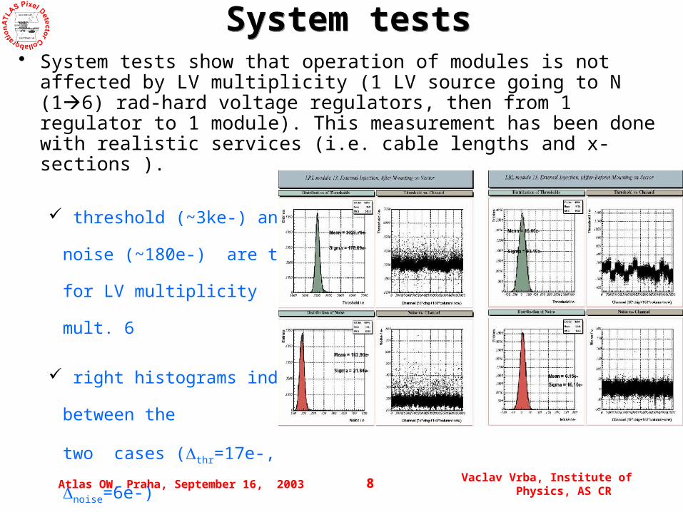
System tests show that operation of modules is not affected by LV multiplicity (1 LV source going to N (16) rad-hard voltage regulators, then from 1 regulator to 1 module). This measurement has been done with realistic services (i.e. cable lengths and x-sections ).
threshold (~3ke-) and noise (~180e-) are the same for LV multiplicity 1 and mult. 6
right histograms indicate difference between the two cases (thr=17e-, noise=6e-)
System testsSystem tests
Atlas OW, Praha, September 16, 2003 Vaclav Vrba, Institute of Physics, AS CR 9
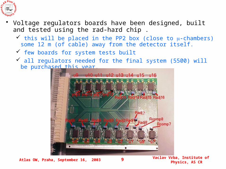
Voltage regulators boards have been designed, built and tested using the rad-hard chip . this will be placed in the PP2 box (close to -chambers) some 12 m
(of cable) away from the detector itself. few boards for system tests built all regulators needed for the final system (5500) will be purchased
this year.
Atlas OW, Praha, September 16, 2003 Vaclav Vrba, Institute of Physics, AS CR 10
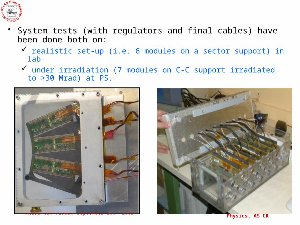
System tests (with regulators and final cables) have been done both on: realistic set-up (i.e. 6 modules on a sector support) in lab under irradiation (7 modules on C-C support irradiated to >30
Mrad) at PS.
Atlas OW, Praha, September 16, 2003 Vaclav Vrba, Institute of Physics, AS CR 11
FE&MCC FDR passed (810 Oct 02) Submissions received back in mid May (FEI2) and on June,6
(MCCI2) many improvements correcting limitations, but… one fault in each design does not allow to use them in the planned
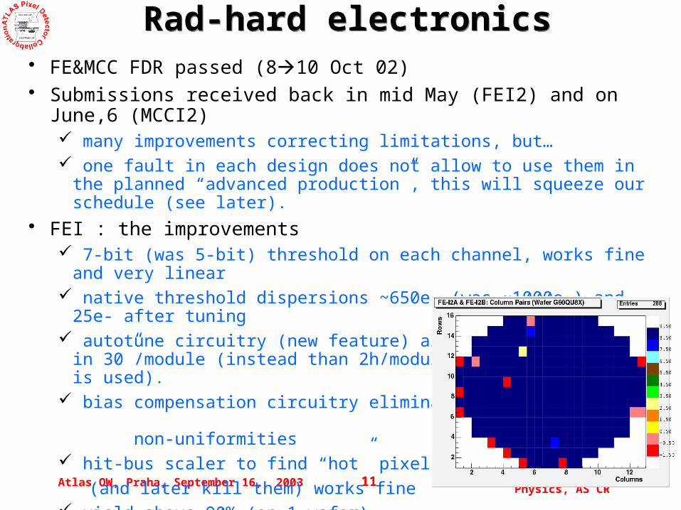
“advanced production”, this will squeeze our schedule (see later). FEI : the improvements
7-bit (was 5-bit) threshold on each channel, works fine and very linear
native threshold dispersions ~650e- (was ~1000e-) and 25e- after tuning
autotune circuitry (new feature) allows to tune to ~50e- in 30”/module (instead than 2h/module if an external PC is used).
bias compensation circuitry eliminates FEI1 non-uniformities
hit-bus scaler to find “hot” pixels (and later kill them) works fine yield above 90% (on 1 wafer), encouraging as we changed IBM foundry from FEI1 to FEI2.
Rad-hard electronicsRad-hard electronics
Atlas OW, Praha, September 16, 2003 Vaclav Vrba, Institute of Physics, AS CR 12
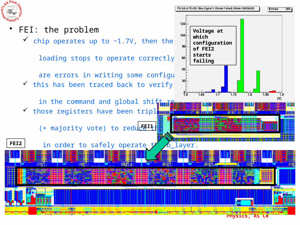
FEI: the problem chip operates up to ~1.7V, then the register
loading stops to operate correctly and there
are errors in writing some configurations. this has been traced back to verify conditions
in the command and global shift registers those registers have been triplicated
(+ majority vote) to reduce the SEU rate
in order to safely operate the b_layer. in doing so, the size of the registers
became much larger.
Voltage at which Voltage at which configuration of configuration of FEI2 starts FEI2 starts failingfailing
FEI1FEI1
FEI2FEI2
Atlas OW, Praha, September 16, 2003 Vaclav Vrba, Institute of Physics, AS CR 13
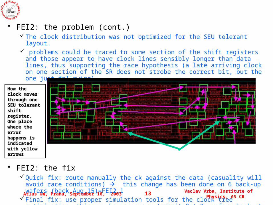
FEI2: the problem (cont.)The clock distribution was not optimized for the SEU tolerant layout. problems could be traced to some section of the shift registers and those
appear to have clock lines sensibly longer than data lines, thus supporting the race hypothesis (a late arriving clock on one section of the SR does not strobe the correct bit, but the one just following)
FEI2: the fix Quick fix: route manually the ck against the data (casuality will avoid race
conditions) this change has been done on 6 back-up wafers (back Aug.15)=FEI2.1
Final fix: use proper simulation tools for the clock tree optimization, this may be necessary (submit Oct.2, wafers back at Nov. 26)= FEI3 (start design NOW)
How the clock How the clock moves through moves through one SEU one SEU tolerant shift tolerant shift register.register.One place One place where the error where the error happens is happens is indicated with indicated with yellow arrowsyellow arrows
Atlas OW, Praha, September 16, 2003 Vaclav Vrba, Institute of Physics, AS CR 14
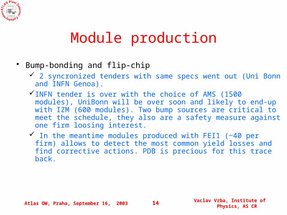
Module production
Bump-bonding and flip-chip 2 syncronized tenders with same specs went out (Uni Bonn and
INFN Genoa). INFN tender is over with the choice of AMS (1500 modules), UniBonn
will be over soon and likely to end-up with IZM (600 modules). Two bump sources are critical to meet the schedule, they also are a safety measure against one firm loosing interest.
In the meantime modules produced with FEI1 (~40 per firm) allows to detect the most common yield losses and find corrective actions. PDB is precious for this trace back.
Atlas OW, Praha, September 16, 2003 Vaclav Vrba, Institute of Physics, AS CR 15
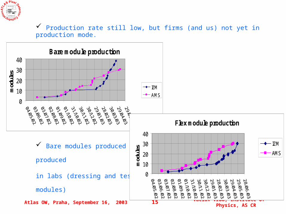
Production rate still low, but firms (and us) not yet in production mode.
Bare modules produced by firms, flex module produced
in labs (dressing and testing bare modules)
Bare module production
0
10
20
30
40
mod
ules
IZM
AMS
Flex module production
0
10
20
30
40m
odul
esIZM
AMS
Atlas OW, Praha, September 16, 2003 Vaclav Vrba, Institute of Physics, AS CR 16
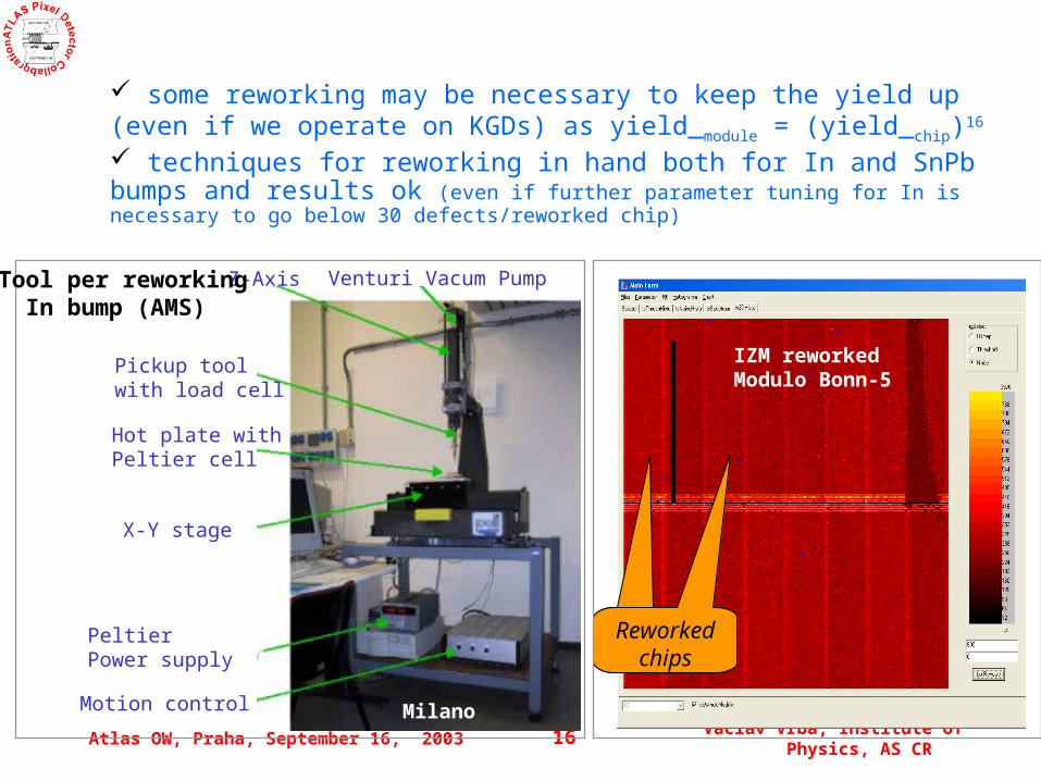
some reworking may be necessary to keep the yield up (even if we operate on KGDs) as yield_module = (yield_chip)16
techniques for reworking in hand both for In and SnPb bumps and results ok (even if further parameter tuning for In is necessary to go below 30 defects/reworked chip)
Reworked chips
Venturi Vacum PumpZ-Axis
Pickup tool with load cell
Hot plate withPeltier cell
X-Y stage
Peltier Power supply
Motion control
IZM reworkedModulo Bonn-5
Tool per reworkingIn bump (AMS)
Milano
Atlas OW, Praha, September 16, 2003 Vaclav Vrba, Institute of Physics, AS CR 17
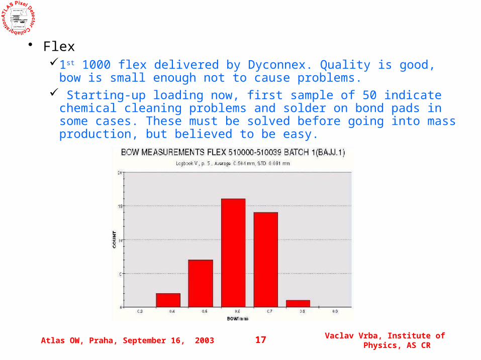
Flex1st 1000 flex delivered by Dyconnex. Quality is good, bow is small
enough not to cause problems. Starting-up loading now, first sample of 50 indicate chemical
cleaning problems and solder on bond pads in some cases. These must be solved before going into mass production, but believed to be easy.
Atlas OW, Praha, September 16, 2003 Vaclav Vrba, Institute of Physics, AS CR 18
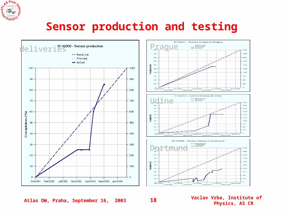
Sensor production and testing
Dortmund
Prague
Udine
deliveries
Atlas OW, Praha, September 16, 2003 Vaclav Vrba, Institute of Physics, AS CR 19
Sensors Sensors
CiS production of 600 good tiles (all tested) done, next 400 delivery to resume next month after factory moved to a new site and restarted.
Tesla recently qualified for the mass production of pixel sensors for ATLAS. Production will start in January 04; end of production in
summer 05. We got a positive answer from both vendors for our request to
extend the option for buying more sensors up to Feb 05.
Atlas OW, Praha, September 16, 2003 Vaclav Vrba, Institute of Physics, AS CR 20
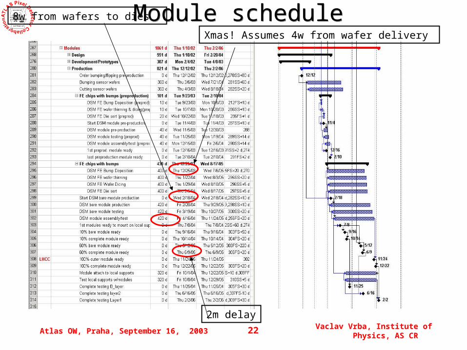
ScheduleSchedule
Advanced production was supposed to happen from summer to Dec03 this would have allowed a smooth start-up of all the (firm+lab) activities
related to module construction would have also allowed to build a couple of disks at least, thus reducing
the pressure on the forthcoming “real” production due to the delay of electronics we may now only hope to begin a smaller
advanced production with the 6 wafers of FEI2.1 this may at most give 1 disk plus the necessary modules to keep going with the qualification of the stave production labs.
all that translates into: delivery of the pixel system delayed by 2 months more compact production schedule with sharper start-up curve (and
therefore more risk) in the following are shown some details of the electronics and module
schedule.
Atlas OW, Praha, September 16, 2003 Vaclav Vrba, Institute of Physics, AS CR 21
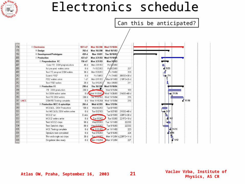
Can this be anticipated?
Electronics scheduleElectronics schedule
Atlas OW, Praha, September 16, 2003 Vaclav Vrba, Institute of Physics, AS CR 22
Module scheduleModule scheduleXmas! Assumes 4w from wafer delivery
8w from wafers to dies
2m delay
Atlas OW, Praha, September 16, 2003 Vaclav Vrba, Institute of Physics, AS CR 23
Conclusions
Achieved technical progress is excellent, it has been demonstrated that pixels can really meet all LHC requirements,
Problems in electronics are not very serious and can certainly be corrected in the timescale indicated.
The sensor production is well in schedule – a half of the production is ready, end of the production in summer 2004.
Due to the present development with FE chips only in Spring04 we will be in position to safely extrapolate to the “ready to install” day.