Embed Size (px)
Citation preview
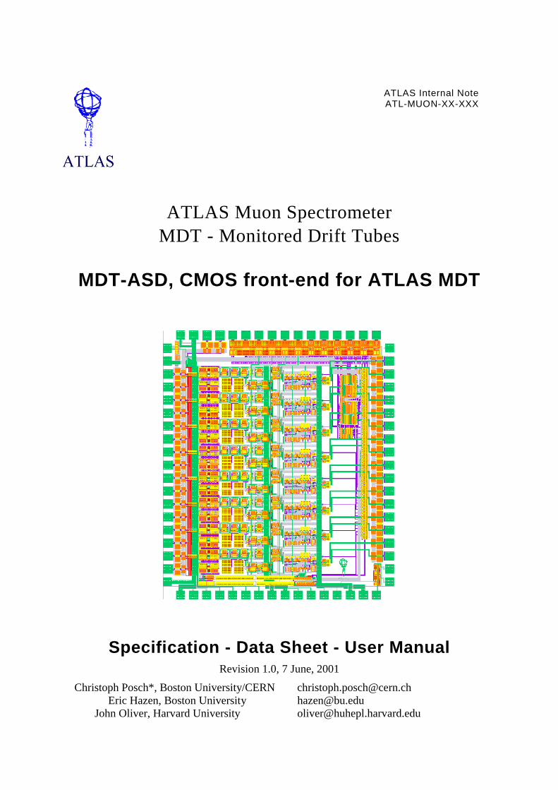
ATLAS Internal NoteATL-MUON-XX-XXX
ATLAS Muon SpectrometerMDT - Monitored Drift Tubes
MDT-ASD, CMOS front-end for ATLAS MDT
Specification - Data Sheet - User ManualRevision 1.0, 7 June, 2001
Christoph Posch*, Boston University/CERN [email protected] Hazen, Boston University [email protected]
John Oliver, Harvard University [email protected]
ATLAS Muon Spectrometer - Monitored Drift TubesASD Amplifier-Shaper-Discriminator IC
Introduction - MDT system overview
2
1 INTRODUCTION...................................................................................................................................4
1.1 MDT SYSTEM OVERVIEW...................................................................................................................41.1.1 General......................................................................................................................................41.1.2 MDT chamber properties ..........................................................................................................41.1.3 Drift gas issues ..........................................................................................................................41.1.4 On-chamber readout electronics ...............................................................................................4
1.2 FRONT END REQUIREMENTS ...............................................................................................................5
2 DESIGN ...................................................................................................................................................6
2.1 OVERVIEW AND SPECIFICATIONS........................................................................................................62.2 FABRICATION PROCESS ......................................................................................................................6
2.2.1 Basic specifications ...................................................................................................................62.2.2 Radiation tolerance ...................................................................................................................7
2.2.2.1 Single event latchup (SEL) ...................................................................................................................72.2.2.2 Total ionizing dose (TID)......................................................................................................................82.2.2.3 Single event upset (SEU) ......................................................................................................................8
2.3 TOPOLOGY AND ARCHITECTURE.........................................................................................................92.4 ANALOG SIGNAL CHAIN....................................................................................................................10
2.4.1 Pre-amplifier ...........................................................................................................................102.4.2 Differential amplifiers .............................................................................................................102.4.3 Shaper......................................................................................................................................112.4.4 Pre-discriminator gain stage...................................................................................................122.4.5 Discriminator ..........................................................................................................................122.4.6 LVDS output cell .....................................................................................................................122.4.7 Analog pad driver....................................................................................................................132.4.8 Wilkinson ADC ........................................................................................................................142.4.9 Input protection .......................................................................................................................14
2.5 SUBCIRCUIT CHARACTERISTICS........................................................................................................152.5.1 Pre-amplifier ...........................................................................................................................152.5.2 Differential amplifier stages DA1 through DA4......................................................................152.5.3 Pre-Amplifier – Shaper: Combined transfer characteristic ....................................................182.5.4 Pre-Amplifier – Shaper: Time domain pulse response............................................................192.5.5 Simulation with GARFIELD signals........................................................................................202.5.6 Wilkinson ADC ........................................................................................................................212.5.7 Analog pad driver....................................................................................................................22
2.6 PROGRAMMABLE PARAMETERS........................................................................................................232.6.1 Programmable analog parameters..........................................................................................23
2.6.1.1 Timing discriminator threshold...........................................................................................................232.6.1.2 Timing discriminator hysteresis ..........................................................................................................242.6.1.3 Wilkinson ADC Control .....................................................................................................................25
2.6.2 Programmable functional parameters.....................................................................................262.6.2.1 Calibration/test pulse injection............................................................................................................262.6.2.2 Chip mode...........................................................................................................................................262.6.2.3 Channel mode .....................................................................................................................................26
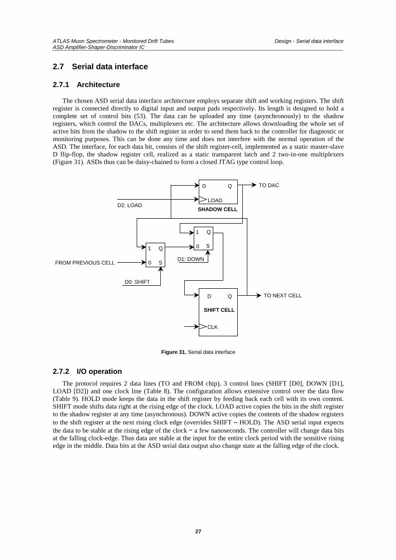
2.7 SERIAL DATA INTERFACE .................................................................................................................272.7.1 Architecture .............................................................................................................................272.7.2 I/O operation ...........................................................................................................................272.7.3 Shift register bit assignment ....................................................................................................28
3 IC LAYOUT ..........................................................................................................................................29
3.1 DIE AND PACKAGING........................................................................................................................293.2 SUBSTRATE NOISE COUPLING ...........................................................................................................29
4 PROTOTYPING - TEST AND MEASUREMENT RESULTS ........................................................30
4.1 SUB-CIRCUITS AND BUILDING BLOCKS .............................................................................................304.1.1 Bipolar shaper.........................................................................................................................304.1.2 Amplifier sensitivity .................................................................................................................314.1.3 Discriminator time slew ..........................................................................................................324.1.4 Wilkinson ADC performance...................................................................................................32
ATLAS Muon Spectrometer - Monitored Drift TubesASD Amplifier-Shaper-Discriminator IC
Introduction - MDT system overview
3
4.1.5 Timing discriminator threshold DAC ......................................................................................334.1.6 Timing discriminator hysteresis DAC .....................................................................................344.1.7 Serial data interface ................................................................................................................34
4.2 SYSTEM PERFORMANCE....................................................................................................................344.2.1 Noise behaviour and non-systematic measurement errors......................................................34
4.2.1.1 Time measurement..............................................................................................................................344.2.1.2 Charge measurement...........................................................................................................................35
4.2.2 Power consumption .................................................................................................................37
5 APPENDIX ............................................................................................................................................38
5.1 MOS TRANSISTOR MODELS..............................................................................................................385.2 LVDS DRIVER PROPERTIES ..............................................................................................................39
5.2.1 Driver DC specifications .........................................................................................................395.2.2 Driver AC specifications .........................................................................................................41
5.3 PACKAGING INFORMATION...............................................................................................................44
6 REFERENCES ......................................................................................................................................45
ATLAS Muon Spectrometer - Monitored Drift TubesASD Amplifier-Shaper-Discriminator IC
Introduction - MDT system overview
4
1 Introduction
1.1 MDT system overview
1.1.1 General
The ATLAS MDT system consists of about 350,000 pressurized drift tubes of 3 cm diameter, withlengths from 1.5 to 6 m. The MDTs are read out by an ASD at one end, and the other end is terminated withthe characteristic impedance of the tube (37� :). The pre-amp input impedance is a relatively low (~ 100:� to maximize collected charge. To minimize cost, the MDT signals are carried on two-layer "hedgehogboards" to a mezzanine board, which contains 24 readout channels: 3 Octal ASDs, a single 24-channel TDC,and associated control circuitry. A single MDT chamber may have as many as 432 drift tubes or 18hedgehog/mezzanine board sets. Data are read out of each TDC individually via a 40 Mbit/sec serial link toa single CSM (Chamber Service Module) which multiplexes the (up to) 18 serial links into a single opticalfiber for transmission to the ATLAS DAQ. A daisy-chain JTAG bus permits downloading of parameters toASDs and TDCs and triggering of test/calibration pulse injection. Each superlayer (3 or 4 layers ofindividual tubes) is entirely enclosed in a faraday cage shield at both ends. All AC signals entering orleaving the shield are low-level differential signals (LVDS). All DC signals are filtered at the shield entrypoint. Each complete MDT chamber is electrically isolated from the support structure, and all services (gas,electrical, etc) are also electrically isolated or floating at the source. The MDT chambers will be individuallygrounded in a controlled way to a single common ground point.
1.1.2 MDT chamber properties
Some properties relevant for the design of the readout electronics of the muon drift tubes are summarizedin Table 1.
Table 1. MDT properties
Length d 6 mDiameter 30 mmWire diameter 50 PmWire resistance 44 : / mImpedance (Z0) 380 :Termination 380 : in series with 470 pFAC coupling capacitor 470 pFDrift gas Ar/CO2 (93%/7%)Maximum background rate 400kHz
1.1.3 Drift gas issues
The drift gas Ar/CO2 93/7 was chosen in large part because of its favourable ageing properties in theLHC environment. It is, however, a non-linear drift gas and this results in some difficulties for the ASDdesign [1]. In particular, the non-linear r-t relationship results in a significant probability of late arrivingclusters. This has been simulated extensively [1][16][17][18], and results in significant after-pulsing of theresulting signal. We expect approximately three output pulses for each muon track and this can result indifficulties for track reconstruction. It has been shown, again by extensive simulation [16][17][18], thatintroducing dead time for entire drift time of the MTD substantially eliminates this problem while minimallyimpacting track reconstruction efficiency. Thus, programmable deadtime, up to 1 Ps, is a requirement of thedesign.
1.1.4 On-chamber readout electronics
The ASD chips are mounted on a “mezzanine” card which is in turn connected to a chamber mounted“hedgehog” card. Each mezzanine card contains three MDT-ASD for a total of 24 channels per mezzanine-hedgehog combination. The hedgehog contains no active circuitry and is fully contained within a faradaycage.
ATLAS Muon Spectrometer - Monitored Drift TubesASD Amplifier-Shaper-Discriminator IC
Introduction - Front end requirements
1.2 Front end requirements
The ATLAS Muon Spectrometer aims for a PT resolution of 10% for 1 TeV muons. This translates into asingle wire resolution requirement of < 80 Pm.
The average drift velocity is about 20 Pm/ns, which implies a systematic timing error for an individualtube of about 500 ps. The planned gas gain is low, about �×104, to avoid aging problems. The expectedsignal (collected charge) is roughly 1500 electrons (0.25 fC) per primary electron, so good positionresolution requires a low noise front-end. A specified pre-amp peaking time of 15 ns is a good compromisein terms of resolution and stability [16][18].
The channel to channel crosstalk is specified to be less than 1%. The high count rates of up to 400kHz/wire together with the long electron drift times require either a bipolar shaping scheme or activebaseline restoration to avoid resolution deterioration due to baseline fluctuations. At the time of the TDR, thebaseline MDT gas was Ar/N2/CH4 91/4/5 (3 bars absolute) which is very linear and has a maximum drifttime of 500 ns. The choice for the ASD shaping scheme was unipolar shaping with active baselinerestoration for the following two reasons [19]. First, it allows the measurement of the signal trailing edge,which has a fixed latency with respect to the bunch crossing, with an accuracy of about 20 ns. Second, itavoids multiple threshold crossings per muon track, which would increase the hit rate and therefore thereadout occupancy. Aging problems with all MDT gases containing hydrocarbons caused a change of thebaseline gas to Ar/CO2 93/7 (3 bars absolute) which has a maximum drift time of 800 ns and is very non-linear [1]. The long drift time and the non-linearity degrade the trailing edge resolution to about 80 ns andcause multiple threshold crossings even for a unipolar shaping scheme. We therefore have adopted a bipolarshaping scheme since it does not require an active BLR and also does not require programmable filter timeconstants [19].
To avoid multiple hits from multiple threshold crossings for a single signal we introduce a variable deadtime up to the maximum drift time. It was shown that the overall increase in dead time does not cause adegradation of the pattern recognition efficiency [1][16].
An ADC will measure the signal charge in a given time window (integration gate) following the initialthreshold crossing. The signal charge is encoded into pulse width using the dual-slope "Wilkinson"technique. This charge information allows for increasing the accuracy of the timing measurement byperforming time slewing correction [16][17], thus improving the spatial resolution of the tracking detector.Additionally, it is effective for diagnostics and monitoring purposes and might also be used for dE/dxidentification of slow moving heavy particles like heavy muon SUSY partners [13]. Two modes of operationwill be provided. In one mode the ASD output gives the time over threshold information, i.e. signal leadingand trailing edge timing. The other mode measures leading edge time and charge and is considered thedefault operating mode.
ATLAS Muon Spectrometer - Monitored Drift TubesASD Amplifier-Shaper-Discriminator IC
Design - Overview and specifications
6
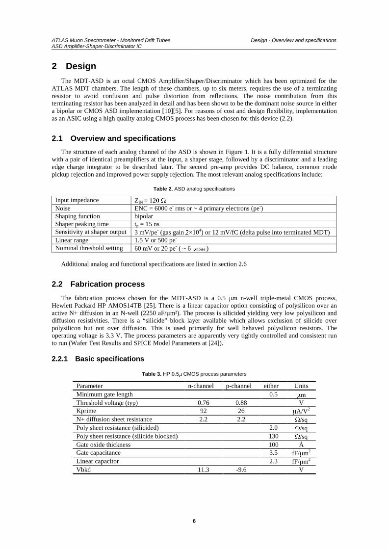
2 Design
The MDT-ASD is an octal CMOS Amplifier/Shaper/Discriminator which has been optimized for theATLAS MDT chambers. The length of these chambers, up to six meters, requires the use of a terminatingresistor to avoid confusion and pulse distortion from reflections. The noise contribution from thisterminating resistor has been analyzed in detail and has been shown to be the dominant noise source in eithera bipolar or CMOS ASD implementation [10][5]. For reasons of cost and design flexibility, implementationas an ASIC using a high quality analog CMOS process has been chosen for this device (2.2).
2.1 Overview and specifications
The structure of each analog channel of the ASD is shown in Figure 1. It is a fully differential structurewith a pair of identical preamplifiers at the input, a shaper stage, followed by a discriminator and a leadingedge charge integrator to be described later. The second pre-amp provides DC balance, common modepickup rejection and improved power supply rejection. The most relevant analog specifications include:
Table 2. ASD analog specifications
Input impedance ZIN = 12� :Noise ENC = 6000 e- rms or ~ 4 primary electrons (pe-)Shaping function bipolarShaper peaking time tp = 15 nsSensitivity at shaper output 3 mV/pe- (gas gain �×104) or 12 mV/fC (delta pulse into terminated MDT)Linear range 1.5 V or 500 pe-
Nominal threshold setting 60 mV or 20 pe- ( ~ 6 Vnoise )
Additional analog and functional specifications are listed in section 2.6
2.2 Fabrication process
The fabrication process chosen for the MDT-ASD is a 0.5 Pm n-well triple-metal CMOS process,Hewlett Packard HP AMOS14TB [25]. There is a linear capacitor option consisting of polysilicon over anactive N+ diffusion in an N-well (2250 aF/µm²). The process is silicided yielding very low polysilicon anddiffusion resistivities. There is a “silicide” block layer available which allows exclusion of silicide overpolysilicon but not over diffusion. This is used primarily for well behaved polysilicon resistors. Theoperating voltage is 3.3 V. The process parameters are apparently very tightly controlled and consistent runto run (Wafer Test Results and SPICE Model Parameters at [24]).
2.2.1 Basic specifications
Table 3. HP 0.5P CMOS process parameters
Parameter n-channel p-channel either UnitsMinimum gate length 0.5 PmThreshold voltage (typ) 0.76 0.88 VKprime 92 26 PA/V2
N+ diffusion sheet resistance 2.2 2.2 :/sqPoly sheet resistance (silicided) 2.0 :/sqPoly sheet resistance (silicide blocked) 130 :/sqGate oxide thickness 100 ÅGate capacitance 3.5 fF/Pm2
Linear capacitor 2.3 fF/Pm2
Vbkd 11.3 -9.6 V
ATLAS Muon Spectrometer - Monitored Drift TubesASD Amplifier-Shaper-Discriminator IC
Design - Fabrication process
7
2.2.2 Radiation tolerance
The MDT-ASD will reside and work in a defined radiation environment. Table 4 gives the simulatedradiation levels for the relevant locations in ATLAS, accumulated over the foreseen lifetime of theexperiment. The inner end-cap chambers (EIS/EIL) will experience the highest levels (bold numbers).
Table 4. Simulated radiation levels (SRL) for MDT electronics locations
BIS/BIL BMS/BML BOS/BOL EIS/EIL EMS/EML EOS/EOLSRLTID (krad) 0.47 0.28 0.13 0.64 0.62 0.33SRLNIEL (1MeV eq n/m2) 0.3u1011 0.3u1011 0.24u1011 2.9u1011 0.34u1011 0.17u1011
SRLSEE (>20MeV h/cm2) 0.54u1010 0.57u1010 0.46u1010 4.8u1010 0.9u1010 0.3u1010
Several studies on total dose and single-event tolerance for devices fabricated on the HP AMOS14TBprocess have been conducted [8][14][15]. Some of the relevant results are summarized below.
2.2.2.1 Single event latchup (SEL)
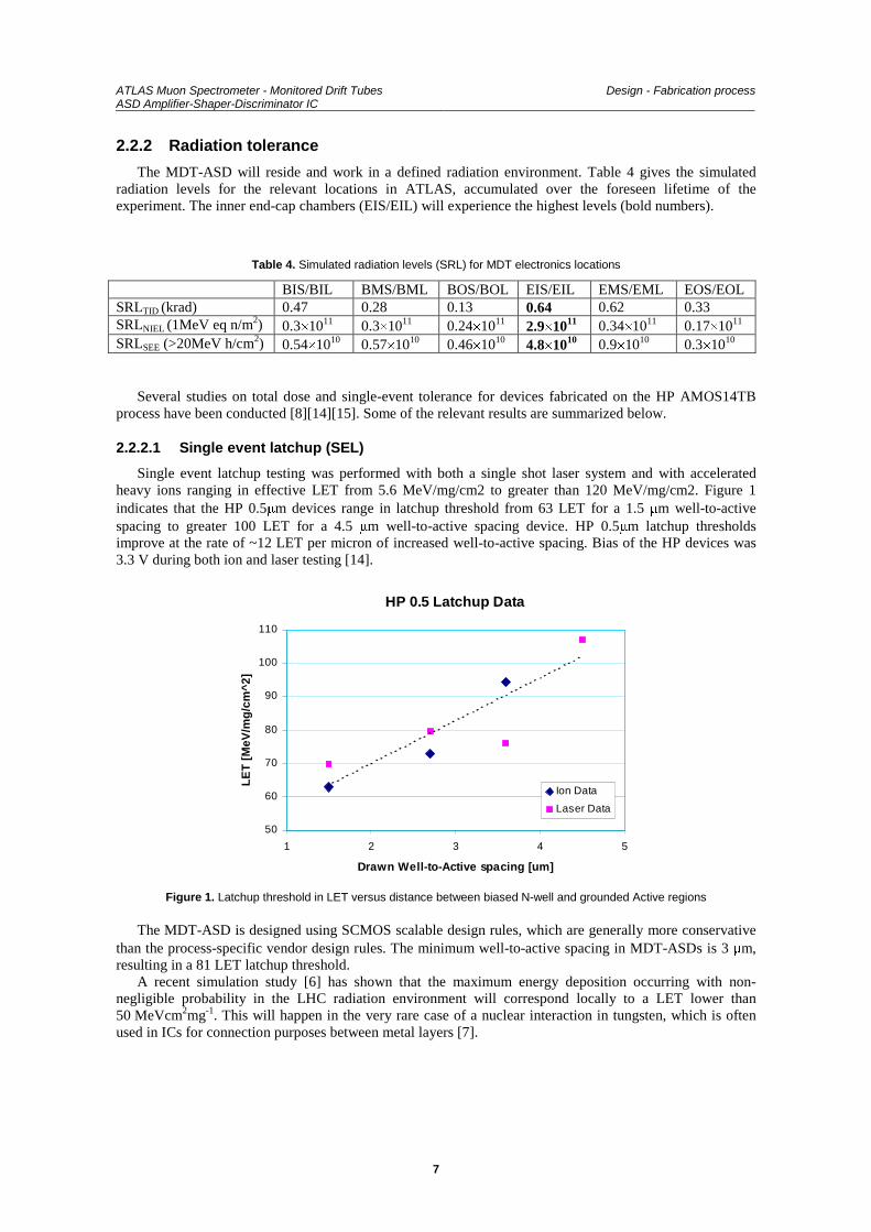
Single event latchup testing was performed with both a single shot laser system and with acceleratedheavy ions ranging in effective LET from 5.6 MeV/mg/cm2 to greater than 120 MeV/mg/cm2. Figure 1indicates that the HP 0.5Pm devices range in latchup threshold from 63 LET for a 1.5 Pm well-to-activespacing to greater 100 LET for a 4.5 Pm well-to-active spacing device. HP 0.5Pm latchup thresholdsimprove at the rate of ~12 LET per micron of increased well-to-active spacing. Bias of the HP devices was3.3 V during both ion and laser testing [14].
HP 0.5 Latchup Data
50
60
70
80
90
100
110
1 2 3 4 5
Drawn Well-to-Active spacing [um]
LE
T [
MeV
/mg
/cm
^2]
Ion Data
Laser Data
Figure 1. Latchup threshold in LET versus distance between biased N-well and grounded Active regions
The MDT-ASD is designed using SCMOS scalable design rules, which are generally more conservativethan the process-specific vendor design rules. The minimum well-to-active spacing in MDT-ASDs is 3 Pm,resulting in a 81 LET latchup threshold.
A recent simulation study [6] has shown that the maximum energy deposition occurring with non-negligible probability in the LHC radiation environment will correspond locally to a LET lower than50 MeVcm2mg-1. This will happen in the very rare case of a nuclear interaction in tungsten, which is oftenused in ICs for connection purposes between metal layers [7].
ATLAS Muon Spectrometer - Monitored Drift TubesASD Amplifier-Shaper-Discriminator IC
Design - Fabrication process
8
2.2.2.2 Total ionizing dose (TID)
Total dose irradiation was performed with a 60Co gamma source at 50 rad (Si)/sec up to 300 krad total.At each measurement point, the devices were measured and irradiation reinitiated within one hour.Following final irradiation, all devices were subjected to a 100q C biased anneal for 168 hours.
Good TID radiation tolerance is achieved in the HP 0.5Pm process. The average change in thresholdvoltage at 100 krad is less than 40 mV for the n-channel and less than 20 mV for the p-channel devices.
Table 5. HP AMOS14TB total ionizing dose (TID) results
Dose Vth NMOS Vth PMOS Gate delay100 krad -40 mV 18 mV +0.6%300 krad -38 mV 43 mV +1.0%
Post-anneal 0 mV 28 mV +1.6%
No special radiation-tolerant layout techniques were applied. The HP 0.5Pm process is recommended tobe a candidate for (space) missions with a total dose requirement of one hundred kilorad [15].
The expected total ionizing dose, calculated from the figures in Table 4 for the worst case location (end-cap inner chambers) in consideration of all relevant safety factors for a known-batch ASIC is 3.5 krad.
2.2.2.3 Single event upset (SEU)
SEU studies on devices fabricated on the HP AMOS14TB production line were conducted. A shiftregister composed of conventional, non-radiation-tolerant, flip-flops exhibited SEU at an LET of 7.0MeV/mg/cm2 and had a saturation cross section of about 9 u 10-7 cm2 per flip-flop [8].
ATLAS Muon Spectrometer - Monitored Drift TubesASD Amplifier-Shaper-Discriminator IC
Design - Topology and architecture
9
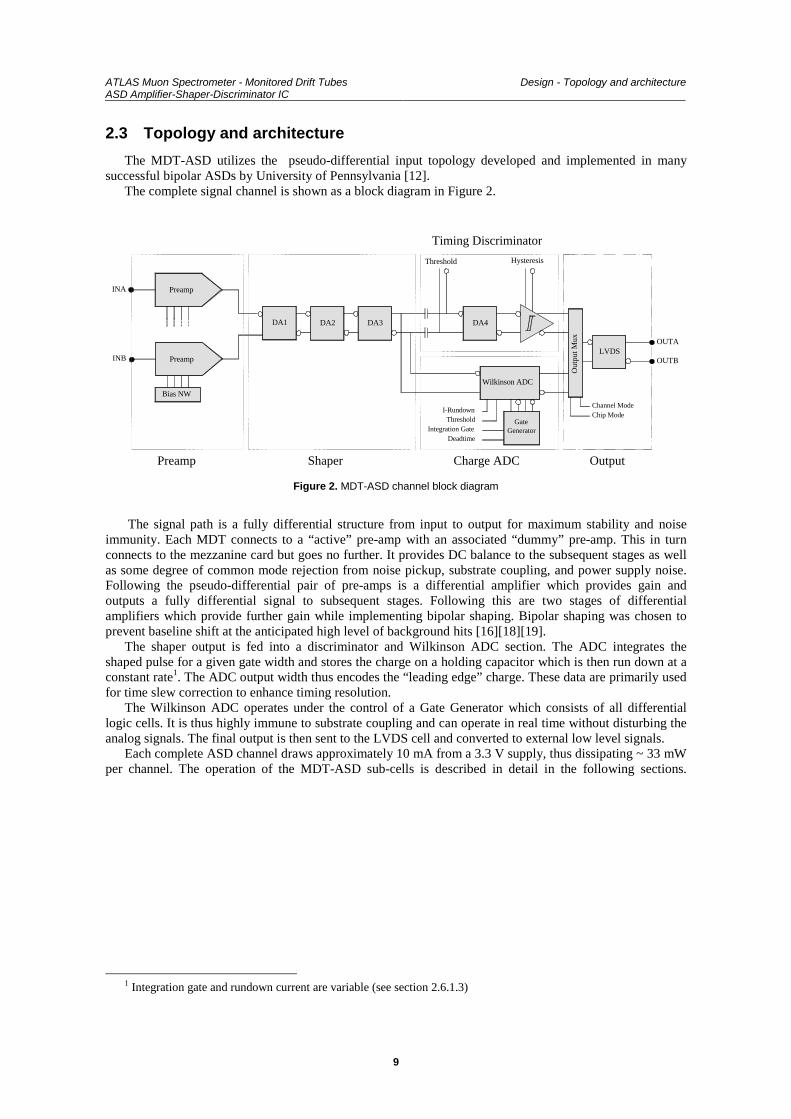
2.3 Topology and architecture
The MDT-ASD utilizes the pseudo-differential input topology developed and implemented in manysuccessful bipolar ASDs by University of Pennsylvania [12].
The complete signal channel is shown as a block diagram in Figure 2.
Preamp
Preamp
DA1 DA2 DA3 DA4
Threshold
Wilkinson ADC
GateGenerator
Out
put M
ux
Hysteresis
Integration GateDeadtime
Bias NW
ThresholdI-Rundown
LVDSOUTA
OUTB
INA
INB
Preamp Shaper
Timing Discriminator
Charge ADC Output
Channel ModeChip Mode
Figure 2. MDT-ASD channel block diagram
The signal path is a fully differential structure from input to output for maximum stability and noiseimmunity. Each MDT connects to a “active” pre-amp with an associated “dummy” pre-amp. This in turnconnects to the mezzanine card but goes no further. It provides DC balance to the subsequent stages as wellas some degree of common mode rejection from noise pickup, substrate coupling, and power supply noise.Following the pseudo-differential pair of pre-amps is a differential amplifier which provides gain andoutputs a fully differential signal to subsequent stages. Following this are two stages of differentialamplifiers which provide further gain while implementing bipolar shaping. Bipolar shaping was chosen toprevent baseline shift at the anticipated high level of background hits [16][18][19].
The shaper output is fed into a discriminator and Wilkinson ADC section. The ADC integrates theshaped pulse for a given gate width and stores the charge on a holding capacitor which is then run down at aconstant rate1. The ADC output width thus encodes the “leading edge” charge. These data are primarily usedfor time slew correction to enhance timing resolution.
The Wilkinson ADC operates under the control of a Gate Generator which consists of all differentiallogic cells. It is thus highly immune to substrate coupling and can operate in real time without disturbing theanalog signals. The final output is then sent to the LVDS cell and converted to external low level signals.
Each complete ASD channel draws approximately 10 mA from a 3.3 V supply, thus dissipating ~ 33 mWper channel. The operation of the MDT-ASD sub-cells is described in detail in the following sections.
1 Integration gate and rundown current are variable (see section 2.6.1.3)
ATLAS Muon Spectrometer - Monitored Drift TubesASD Amplifier-Shaper-Discriminator IC
Design - Analog signal chain
10
2.4 Analog signal chain
2.4.1 Pre-amplifier
Specifications
x Power dissipation: 3.3 mW per pre-amp (~ 1 mA @ 3.3 V)x ZIN: 120 ohms (DC & AC/dynamic)x Charge gain: 1 mV/fCx DC voltage gain: 100 (40dB)x Input noise density: 1.3 nV/ Hzx ENC (with 380 : termination): 6000 e- rms
Description
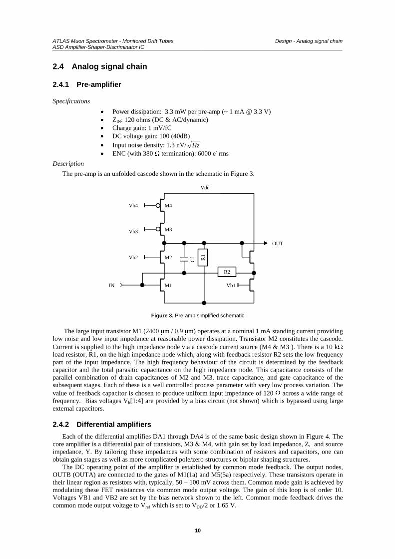
The pre-amp is an unfolded cascode shown in the schematic in Figure 3.
M1
M3
M4
Vdd
IN
OUT
M2
R2
Cf
Vb1
Vb2
Vb3
Vb4R
1
Figure 3. Pre-amp simplified schematic
The large input transistor M1 (2400 Pm / 0.9 Pm) operates at a nominal 1 mA standing current providinglow noise and low input impedance at reasonable power dissipation. Transistor M2 constitutes the cascode.Current is supplied to the high impedance node via a cascode current source (M4 & M3 ). There is a 10 k:load resistor, R1, on the high impedance node which, along with feedback resistor R2 sets the low frequencypart of the input impedance. The high frequency behaviour of the circuit is determined by the feedbackcapacitor and the total parasitic capacitance on the high impedance node. This capacitance consists of theparallel combination of drain capacitances of M2 and M3, trace capacitance, and gate capacitance of thesubsequent stages. Each of these is a well controlled process parameter with very low process variation. Thevalue of feedback capacitor is chosen to produce uniform input impedance of 120 : across a wide range offrequency. Bias voltages Vb[1:4] are provided by a bias circuit (not shown) which is bypassed using largeexternal capacitors.
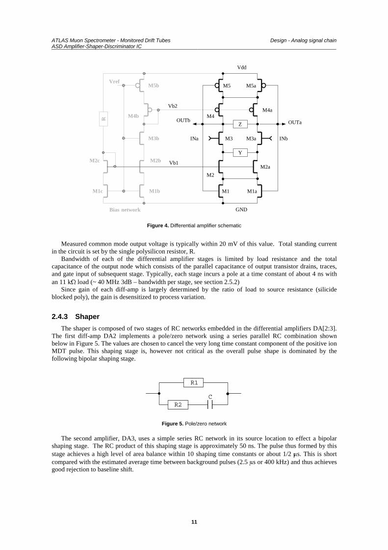
2.4.2 Differential amplifiers
Each of the differential amplifies DA1 through DA4 is of the same basic design shown in Figure 4. Thecore amplifier is a differential pair of transistors, M3 & M4, with gain set by load impedance, Z, and sourceimpedance, Y. By tailoring these impedances with some combination of resistors and capacitors, one canobtain gain stages as well as more complicated pole/zero structures or bipolar shaping structures.
The DC operating point of the amplifier is established by common mode feedback. The output nodes,OUTB (OUTA) are connected to the gates of M1(1a) and M5(5a) respectively. These transistors operate intheir linear region as resistors with, typically, 50 – 100 mV across them. Common mode gain is achieved bymodulating these FET resistances via common mode output voltage. The gain of this loop is of order 10.Voltages VB1 and VB2 are set by the bias network shown to the left. Common mode feedback drives thecommon mode output voltage to Vref which is set to VDD/2 or 1.65 V.
ATLAS Muon Spectrometer - Monitored Drift TubesASD Amplifier-Shaper-Discriminator IC
Design - Analog signal chain
11
Z
Y
M1
M2
M3a
M4
M5
Vdd
GND
INa INb
OUTb OUTa
Vb1
Vb2
M5a
M4a
M3
M2a
M1a
R
VrefM5b
M4b
M3b
M2b
M1b
Bias network
M1c
M2c
Figure 4. Differential amplifier schematic
Measured common mode output voltage is typically within 20 mV of this value. Total standing currentin the circuit is set by the single polysilicon resistor, R.
Bandwidth of each of the differential amplifier stages is limited by load resistance and the totalcapacitance of the output node which consists of the parallel capacitance of output transistor drains, traces,and gate input of subsequent stage. Typically, each stage incurs a pole at a time constant of about 4 ns withan 11 k: load (~ 40 MHz 3dB – bandwidth per stage, see section 2.5.2)
Since gain of each diff-amp is largely determined by the ratio of load to source resistance (silicideblocked poly), the gain is desensitized to process variation.
2.4.3 Shaper
The shaper is composed of two stages of RC networks embedded in the differential amplifiers DA[2:3].The first diff-amp DA2 implements a pole/zero network using a series parallel RC combination shownbelow in Figure 5. The values are chosen to cancel the very long time constant component of the positive ionMDT pulse. This shaping stage is, however not critical as the overall pulse shape is dominated by thefollowing bipolar shaping stage.
R1
R2C
Figure 5. Pole/zero network
The second amplifier, DA3, uses a simple series RC network in its source location to effect a bipolarshaping stage. The RC product of this shaping stage is approximately 50 ns. The pulse thus formed by thisstage achieves a high level of area balance within 10 shaping time constants or about 1/2 Ps. This is shortcompared with the estimated average time between background pulses (2.5 Ps or 400 kHz) and thus achievesgood rejection to baseline shift.
ATLAS Muon Spectrometer - Monitored Drift TubesASD Amplifier-Shaper-Discriminator IC
Design - Analog signal chain
12
2.4.4 Pre-discriminator gain stage
The shaper output is AC coupled to one additional differential amplifier, DA4, referred to as pre-discriminator gain stage which provides additional gain to the discriminator. This stage has smaller loadresistance (5.5 k:) to provide lower driving impedance to the subsequent discriminator stage. Its sourceresistor is chosen to be zero to provide maximum gain and bandwidth at the expense of higher processvariation of gain. Since the threshold is applied at its input however, the gain sensitivity to process variationis irrelevant.
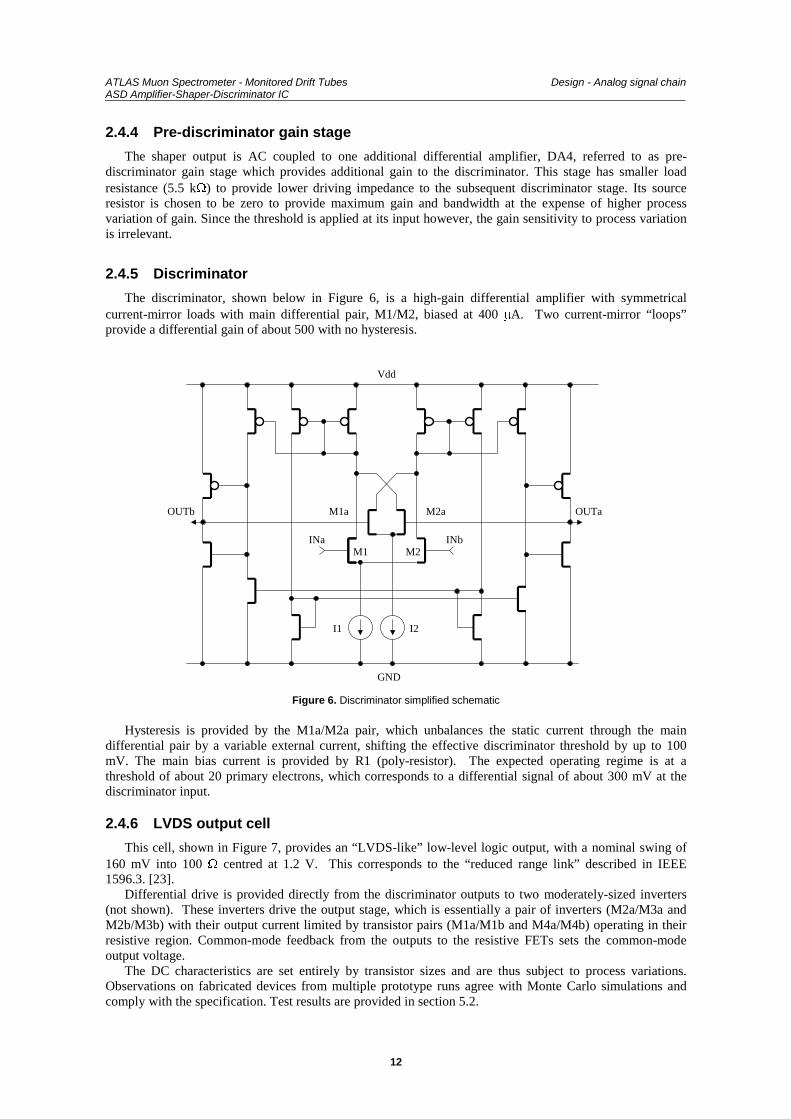
2.4.5 Discriminator
The discriminator, shown below in Figure 6, is a high-gain differential amplifier with symmetricalcurrent-mirror loads with main differential pair, M1/M2, biased at 400 PA. Two current-mirror “loops”provide a differential gain of about 500 with no hysteresis.
INa INb
OUTb OUTa
M1 M2
M1a M2a
Vdd
GND
I1 I2
Figure 6. Discriminator simplified schematic
Hysteresis is provided by the M1a/M2a pair, which unbalances the static current through the maindifferential pair by a variable external current, shifting the effective discriminator threshold by up to 100mV. The main bias current is provided by R1 (poly-resistor). The expected operating regime is at athreshold of about 20 primary electrons, which corresponds to a differential signal of about 300 mV at thediscriminator input.
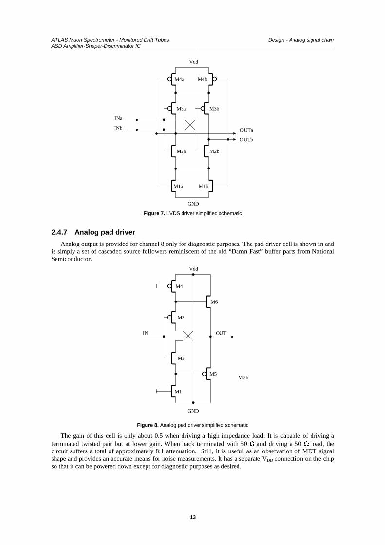
2.4.6 LVDS output cell
This cell, shown in Figure 7, provides an “LVDS-like” low-level logic output, with a nominal swing of160 mV into 100 : centred at 1.2 V. This corresponds to the “reduced range link” described in IEEE1596.3. [23].
Differential drive is provided directly from the discriminator outputs to two moderately-sized inverters(not shown). These inverters drive the output stage, which is essentially a pair of inverters (M2a/M3a andM2b/M3b) with their output current limited by transistor pairs (M1a/M1b and M4a/M4b) operating in theirresistive region. Common-mode feedback from the outputs to the resistive FETs sets the common-modeoutput voltage.
The DC characteristics are set entirely by transistor sizes and are thus subject to process variations.Observations on fabricated devices from multiple prototype runs agree with Monte Carlo simulations andcomply with the specification. Test results are provided in section 5.2.
ATLAS Muon Spectrometer - Monitored Drift TubesASD Amplifier-Shaper-Discriminator IC
Design - Analog signal chain
13
M1a
M2b
M4a
Vdd
GND
OUTa
M4b
M3b
M2a
M1b
M3a
INa
INb
OUTb
Figure 7. LVDS driver simplified schematic
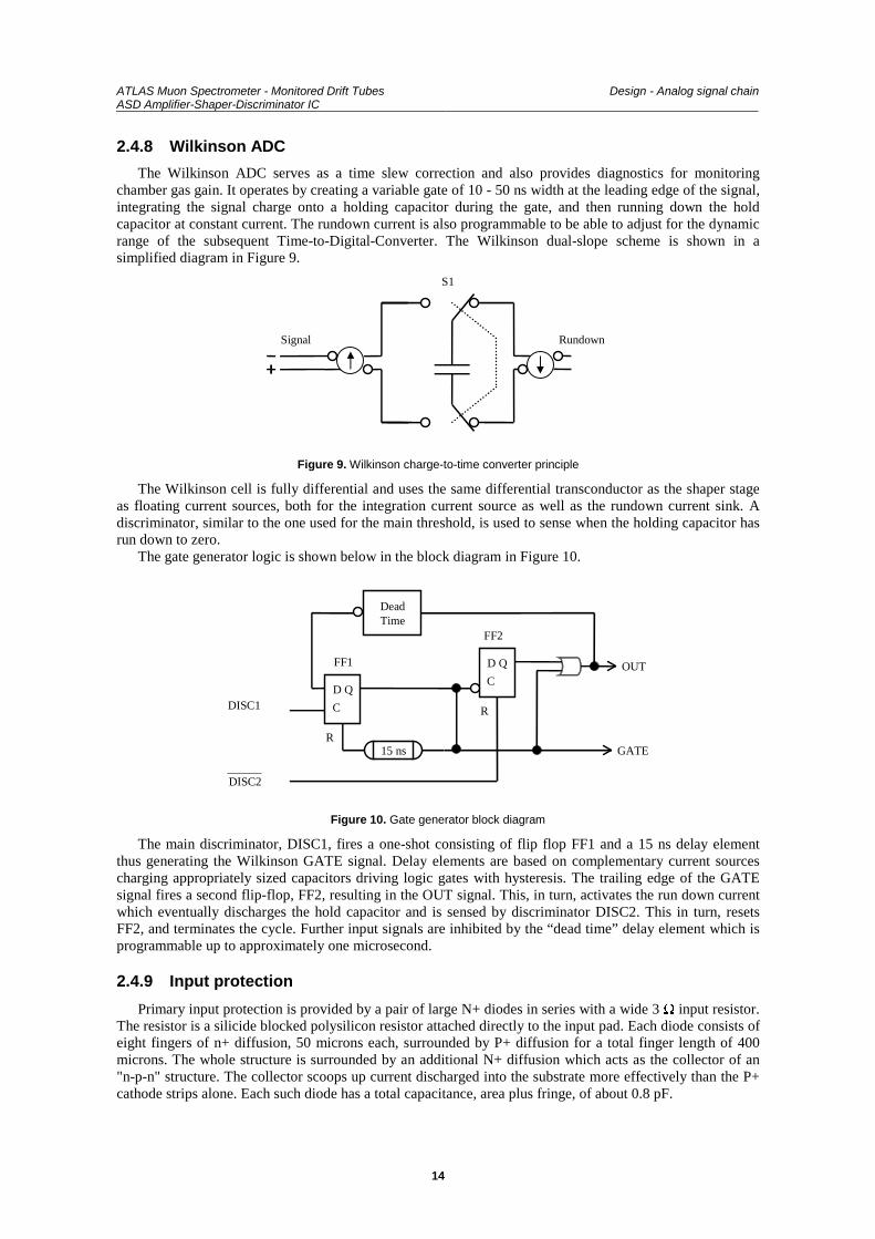
2.4.7 Analog pad driver
Analog output is provided for channel 8 only for diagnostic purposes. The pad driver cell is shown in andis simply a set of cascaded source followers reminiscent of the old “Damn Fast” buffer parts from NationalSemiconductor.
M1
M2b
M4
Vdd
GND
OUT
M2
M3
IN
M5
M6
Figure 8. Analog pad driver simplified schematic
The gain of this cell is only about 0.5 when driving a high impedance load. It is capable of driving aterminated twisted pair but at lower gain. When back terminated with 50 : and driving a 50 : load, thecircuit suffers a total of approximately 8:1 attenuation. Still, it is useful as an observation of MDT signalshape and provides an accurate means for noise measurements. It has a separate VDD connection on the chipso that it can be powered down except for diagnostic purposes as desired.
ATLAS Muon Spectrometer - Monitored Drift TubesASD Amplifier-Shaper-Discriminator IC
Design - Analog signal chain
14
2.4.8 Wilkinson ADC
The Wilkinson ADC serves as a time slew correction and also provides diagnostics for monitoringchamber gas gain. It operates by creating a variable gate of 10 - 50 ns width at the leading edge of the signal,integrating the signal charge onto a holding capacitor during the gate, and then running down the holdcapacitor at constant current. The rundown current is also programmable to be able to adjust for the dynamicrange of the subsequent Time-to-Digital-Converter. The Wilkinson dual-slope scheme is shown in asimplified diagram in Figure 9.
Signal Rundown
S1
Figure 9. Wilkinson charge-to-time converter principle
The Wilkinson cell is fully differential and uses the same differential transconductor as the shaper stageas floating current sources, both for the integration current source as well as the rundown current sink. Adiscriminator, similar to the one used for the main threshold, is used to sense when the holding capacitor hasrun down to zero.
The gate generator logic is shown below in the block diagram in Figure 10.
D Q
C
15 ns
D Q
C
R
R
DeadTime
DISC1
DISC2
OUT
GATE
FF1
FF2
Figure 10. Gate generator block diagram
The main discriminator, DISC1, fires a one-shot consisting of flip flop FF1 and a 15 ns delay elementthus generating the Wilkinson GATE signal. Delay elements are based on complementary current sourcescharging appropriately sized capacitors driving logic gates with hysteresis. The trailing edge of the GATEsignal fires a second flip-flop, FF2, resulting in the OUT signal. This, in turn, activates the run down currentwhich eventually discharges the hold capacitor and is sensed by discriminator DISC2. This in turn, resetsFF2, and terminates the cycle. Further input signals are inhibited by the “dead time” delay element which isprogrammable up to approximately one microsecond.
2.4.9 Input protection
Primary input protection is provided by a pair of large N+ diodes in series with a wide 3 : input resistor.The resistor is a silicide blocked polysilicon resistor attached directly to the input pad. Each diode consists ofeight fingers of n+ diffusion, 50 microns each, surrounded by P+ diffusion for a total finger length of 400microns. The whole structure is surrounded by an additional N+ diffusion which acts as the collector of an"n-p-n" structure. The collector scoops up current discharged into the substrate more effectively than the P+cathode strips alone. Each such diode has a total capacitance, area plus fringe, of about 0.8 pF.
ATLAS Muon Spectrometer - Monitored Drift TubesASD Amplifier-Shaper-Discriminator IC
Design - Analog signal chain
15
There is also a smaller pair of P+ diodes connected to the positive supply rail. In principle, a human bodymodel type discharge into these diodes would dump current into the positive supply rail which, therefore,requires a clamp for bare chip handling. This clamp is based on the UMC “Corner” design [24], but is a bitsimpler. It is by no means, guaranteed to withstand a full HBM discharge while the device is unconnected.
While these diodes are robust, they are not sufficient to withstand a full 3 kV – 4 kV MTD chamberdischarge which can be of order several amperes. Additional off-chip protection in the form of back to back1N914 signal diodes, in conjunction with the on-chip diodes, has been shown to provide robust protectionagainst such discharges.
All digital I/O pads are taken from the MOSIS Hi-ESD Pad Library for the HP AMOS14B process [26].
2.5 Subcircuit characteristics
2.5.1 Pre-amplifier
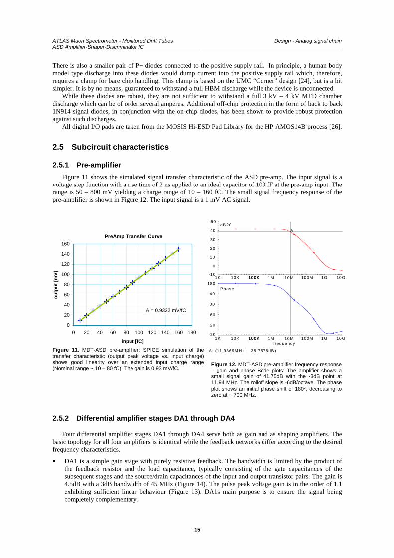
Figure 11 shows the simulated signal transfer characteristic of the ASD pre-amp. The input signal is avoltage step function with a rise time of 2 ns applied to an ideal capacitor of 100 fF at the pre-amp input. Therange is 50 – 800 mV yielding a charge range of 10 – 160 fC. The small signal frequency response of thepre-amplifier is shown in Figure 12. The input signal is a 1 mV AC signal.
PreAmp Transfer Curve
A = 0.9322 mV/fC
0
20
40
60
80
100
120
140
160
0 20 40 60 80 100 120 140 160 180
input [fC]
ou
tpu
t [m
V]
Figure 11. MDT-ASD pre-amplifier: SPICE simulation of thetransfer characteristic (output peak voltage vs. input charge)shows good linearity over an extended input charge range(Nominal range ~ 10 – 80 fC). The gain is 0.93 mV/fC.
50
40
30
20
10
0
-10
180
40
00
60
20
-201K 10K 100K 1M 10M100K 100M 1G 10G
frequency
1K 10K 100K 1M 10M100K 100M 1G 10G
A : (11.9369M H z 38.7578dB )
dB 20
P hase
Figure 12. MDT-ASD pre-amplifier frequency response– gain and phase Bode plots: The amplifier shows asmall signal gain of 41.75dB with the -3dB point at11.94 MHz. The rolloff slope is -6dB/octave. The phaseplot shows an initial phase shift of 180q, decreasing tozero at ~ 700 MHz.
2.5.2 Differential amplifier stages DA1 through DA4
Four differential amplifier stages DA1 through DA4 serve both as gain and as shaping amplifiers. Thebasic topology for all four amplifiers is identical while the feedback networks differ according to the desiredfrequency characteristics.
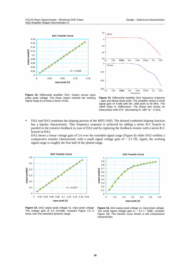
� DA1 is a simple gain stage with purely resistive feedback. The bandwidth is limited by the product ofthe feedback resistor and the load capacitance, typically consisting of the gate capacitances of thesubsequent stages and the source/drain capacitances of the input and output transistor pairs. The gain is4.5dB with a 3dB bandwidth of 45 MHz (Figure 14). The pulse peak voltage gain is in the order of 1.1exhibiting sufficient linear behaviour (Figure 13). DA1s main purpose is to ensure the signal beingcompletely complementary.
ATLAS Muon Spectrometer - Monitored Drift TubesASD Amplifier-Shaper-Discriminator IC
Design - Subcircuit characteristics
16
DA1 Transfer Curve
G = 1.1026
0
0.02
0.04
0.06
0.08
0.1
0.12
0.14
0.16
0.18
0 0.04 0.08 0.12 0.16
input peak [V]
ou
tpu
t p
eak[
V]
Figure 13. Differential amplifier DA1: Output versus inputpulse peak voltage. The linear region extends the workingsignal range by at least a factor of two.
20
0
-20
-40
-60
dB20
0
-100
-200
-3001K 10K 100K 1M 10M100K 100M 1G 10G
frequency
1K 10K 100K 1M 10M100K 100M 1G 10G
Phase
Figure 14. Differential amplifier DA1 frequency response– gain and phase Bode plots: The amplifier shows a smallsignal gain of 4.5dB with the -3dB point at 45 MHz. Therolloff slope is -6dB/octave. The phase plot shows aninitial phase shift of 0q, decreasing to -180q at ~ 3 GHz.
� DA2 and DA3 constitute the shaping portion of the MDT-ASD. The desired combined shaping functionhas a bipolar characteristic. This frequency response is achieved by adding a series R-C branch inparallel to the resistive feedback in case of DA2 and by replacing the feedback resistor with a series R-Cbranch in DA3.DA2 shows a linear voltage gain of 3.4 over the extended signal range (Figure 6) while DA3 exhibits acompressive transfer characteristic with a small signal voltage gain of ~ 3.2 [9]. Again, the workingsignal range is roughly the first half of the plotted range.
DA2 Transfer Curve
G = 3.4127
0
0.1
0.2
0.3
0.4
0.5
0.6
0 0.02 0.04 0.06 0.08 0.1 0.12 0.14 0.16 0.18
input peak [V]
ou
tpu
t p
eak[
V]
Figure 15. DA2 output peak voltage vs. input peak voltageThe voltage gain of 3.4 (10.6dB, compare Figure 17) islinear over the extended dynamic range.
DA3 Transfer Curve
0
0.1
0.2
0.3
0.4
0.5
0.6
0.7
0.8
0.9
1
0 0.1 0.2 0.3 0.4 0.5 0.6
input peak [V]
ou
tpu
t p
eak[
V]
Figure 16. DA3 output peak voltage vs. input peak voltage.The small signal voltage gain is ~ 3.2 (~ 10dB, compareFigure 18). The transfer curve shows a soft compressivecharacteristic.
ATLAS Muon Spectrometer - Monitored Drift TubesASD Amplifier-Shaper-Discriminator IC
Design - Subcircuit characteristics
17
1K 10K 100K 1M 10M100K 100M 1G 10Gfrequency
10K 100K 1M 10M100K 100M 1G 10G
20
10
0
-10
dB20
1K
0
-20
-40
-60
20
40
60Phase
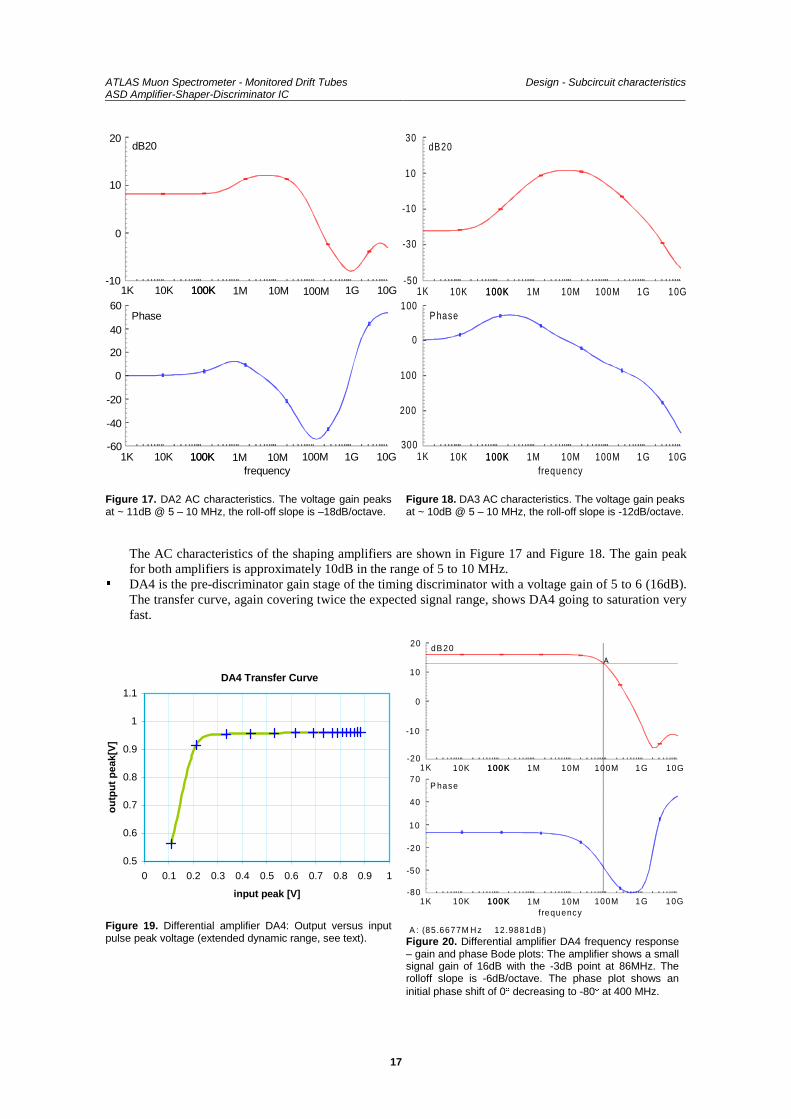
Figure 17. DA2 AC characteristics. The voltage gain peaksat ~ 11dB @ 5 – 10 MHz, the roll-off slope is –18dB/octave.
30
10
-10
-30
-50
100
0
100
200
3001K 10K 100K 1M 10M100K 100M 1G 10G
frequency
1K 10K 100K 1M 10M100K 100M 1G 10G
dB20
P hase
Figure 18. DA3 AC characteristics. The voltage gain peaksat ~ 10dB @ 5 – 10 MHz, the roll-off slope is -12dB/octave.
The AC characteristics of the shaping amplifiers are shown in Figure 17 and Figure 18. The gain peakfor both amplifiers is approximately 10dB in the range of 5 to 10 MHz.
� DA4 is the pre-discriminator gain stage of the timing discriminator with a voltage gain of 5 to 6 (16dB).The transfer curve, again covering twice the expected signal range, shows DA4 going to saturation veryfast.
DA4 Transfer Curve
0.5
0.6
0.7
0.8
0.9
1
1.1
0 0.1 0.2 0.3 0.4 0.5 0.6 0.7 0.8 0.9 1
input peak [V]
ou
tpu
t p
eak[
V]
Figure 19. Differential amplifier DA4: Output versus inputpulse peak voltage (extended dynamic range, see text).
20
10
0
-10
-20
70
10
-20
-50
40
-801K 10K 100K 1M 10M100K 100M 1G 10G
frequency
A : (85.6677M H z 12 .9881dB )
dB 20
P hase
1K 10K 100K 1M 10M100K 100M 1G 10G
Figure 20. Differential amplifier DA4 frequency response– gain and phase Bode plots: The amplifier shows a smallsignal gain of 16dB with the -3dB point at 86MHz. Therolloff slope is -6dB/octave. The phase plot shows aninitial phase shift of 0q decreasing to -80q at 400 MHz.
ATLAS Muon Spectrometer - Monitored Drift TubesASD Amplifier-Shaper-Discriminator IC
Design - Subcircuit characteristics
18
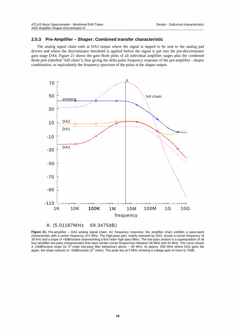
2.5.3 Pre-Amplifier – Shaper: Combined transfer characteristic
The analog signal chain ends at DA3 output where the signal is tapped to be sent to the analog paddrivers and where the discriminator threshold is applied before the signal is put into the pre-discriminatorgain stage DA4. Figure 21 shows the gain Bode plots of all individual amplifier stages plus the combinedBode plot (labelled "full chain"), thus giving the delta pulse frequency response of the pre-amplifier - shapercombination, or equivalently the frequency spectrum of the pulse at the shaper output.
1K 10K 100K 1M 10M100K 100M 1G 10G
frequency
30
10
-10
-30
-50
50
70
-70
-90
-110
A: (5.01187MHz 69.3475dB)
pream p
DA1
DA2
DA3
full chain
Figure 21. Pre-amplifier – DA3 analog signal chain: AC frequency response; the amplifier chain exhibits a pass-bandcharacteristic with a center frequency of 5 MHz. The high-pass part, mainly imposed by DA3, shows a corner frequency of30 kHz and a slope of +6dB/octave (representing a first order high-pass filter). The low-pass section is a superposition of allfour amplifier low-pass characteristics that have similar corner frequencies between 38 MHz and 44 MHz. The curve showsa -24dB/octave slope (or 4th-order low-pass filter behaviour) above ~ 45 MHz. At approx. 500 MHz where DA2 goes flatagain, the slope reduces to -18dB/octave (3rd order). The peak lies at 5 MHz showing a voltage gain of close to 70dB.
ATLAS Muon Spectrometer - Monitored Drift TubesASD Amplifier-Shaper-Discriminator IC
Design - Subcircuit characteristics
19
2.5.4 Pre-Amplifier – Shaper: Time domain pulse response
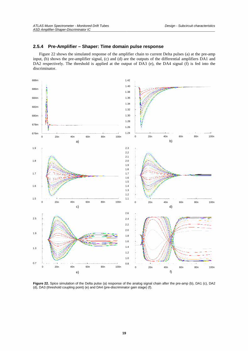
Figure 22 shows the simulated response of the amplifier chain to current Delta pulses (a) at the pre-ampinput, (b) shows the pre-amplifier signal, (c) and (d) are the outputs of the differential amplifiers DA1 andDA2 respectively. The threshold is applied at the output of DA3 (e), the DA4 signal (f) is fed into thediscriminator.
a) b)
c) d)
e) f)
Figure 22. Spice simulation of the Delta pulse (a) response of the analog signal chain after the pre-amp (b), DA1 (c), DA2(d), DA3 (threshold coupling point) (e) and DA4 (pre-discriminator gain stage) (f).
686m
684m
682m
680m
678m
676m0 20n 40n 60n 80n 100n 0 20n 40n 60n 80n 100n
0 20n 40n 60n 80n 100n 0 20n 40n 60n 80n 100n
0 20n 40n 60n 80n 100n 0 20n 40n 60n 80n 100n
1.40
1.38
1.36
1.34
1.32
1.30
688m
1.28
1.26
1.24
1.42
1.9
1.8
1.7
1.6
1.5
2.2
2.1
2.0
1.9
1.8
1.7
1.6
1.5
1.4
2.3
1.3
1.2
1.1
2.5
1.9
1.3
0.7
2.4
2.2
2.0
1.8
1.2
1.6
1.4
2.6
1.0
0.8
ATLAS Muon Spectrometer - Monitored Drift TubesASD Amplifier-Shaper-Discriminator IC
Design - Subcircuit characteristics
20
2.5.5 Simulation with GARFIELD signals
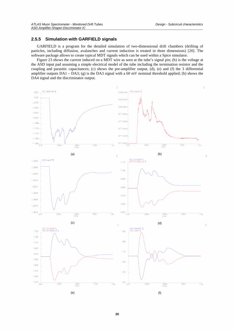
GARFIELD is a program for the detailed simulation of two-dimensional drift chambers (drifting ofparticles, including diffusion, avalanches and current induction is treated in three dimensions) [20]. Thesoftware package allows to create typical MDT signals which can be used within a Spice simulator.
Figure 23 shows the current induced on a MDT wire as seen at the tube’s signal pin; (b) is the voltage atthe ASD input pad assuming a simple electrical model of the tube including the termination resistor and thecoupling and parasitic capacitances; (c) shows the pre-amplifier output, (d), (e) and (f) the 3 differentialamplifier outputs DA1 – DA3; (g) is the DA3 signal with a 60 mV nominal threshold applied; (h) shows theDA4 signal and the discriminator output.
(a) (b)
(c) (d)
(e) (f)
ATLAS Muon Spectrometer - Monitored Drift TubesASD Amplifier-Shaper-Discriminator IC
Design - Subcircuit characteristics
21
(g) (h)
Figure 23. Response of one ASD channel to a MDT current signal created by GARFIELD [20].
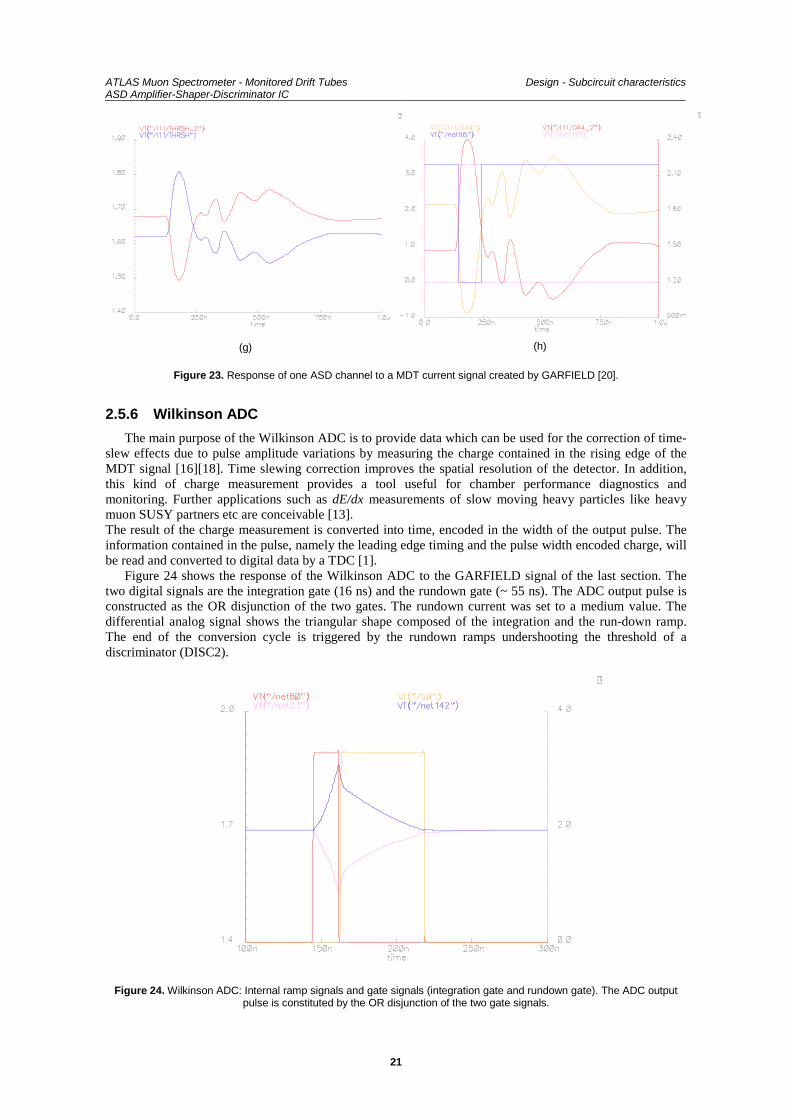
2.5.6 Wilkinson ADC
The main purpose of the Wilkinson ADC is to provide data which can be used for the correction of time-slew effects due to pulse amplitude variations by measuring the charge contained in the rising edge of theMDT signal [16][18]. Time slewing correction improves the spatial resolution of the detector. In addition,this kind of charge measurement provides a tool useful for chamber performance diagnostics andmonitoring. Further applications such as dE/dx measurements of slow moving heavy particles like heavymuon SUSY partners etc are conceivable [13].The result of the charge measurement is converted into time, encoded in the width of the output pulse. Theinformation contained in the pulse, namely the leading edge timing and the pulse width encoded charge, willbe read and converted to digital data by a TDC [1].
Figure 24 shows the response of the Wilkinson ADC to the GARFIELD signal of the last section. Thetwo digital signals are the integration gate (16 ns) and the rundown gate (~ 55 ns). The ADC output pulse isconstructed as the OR disjunction of the two gates. The rundown current was set to a medium value. Thedifferential analog signal shows the triangular shape composed of the integration and the run-down ramp.The end of the conversion cycle is triggered by the rundown ramps undershooting the threshold of adiscriminator (DISC2).
Figure 24. Wilkinson ADC: Internal ramp signals and gate signals (integration gate and rundown gate). The ADC outputpulse is constituted by the OR disjunction of the two gate signals.
ATLAS Muon Spectrometer - Monitored Drift TubesASD Amplifier-Shaper-Discriminator IC
Design - Subcircuit characteristics
22
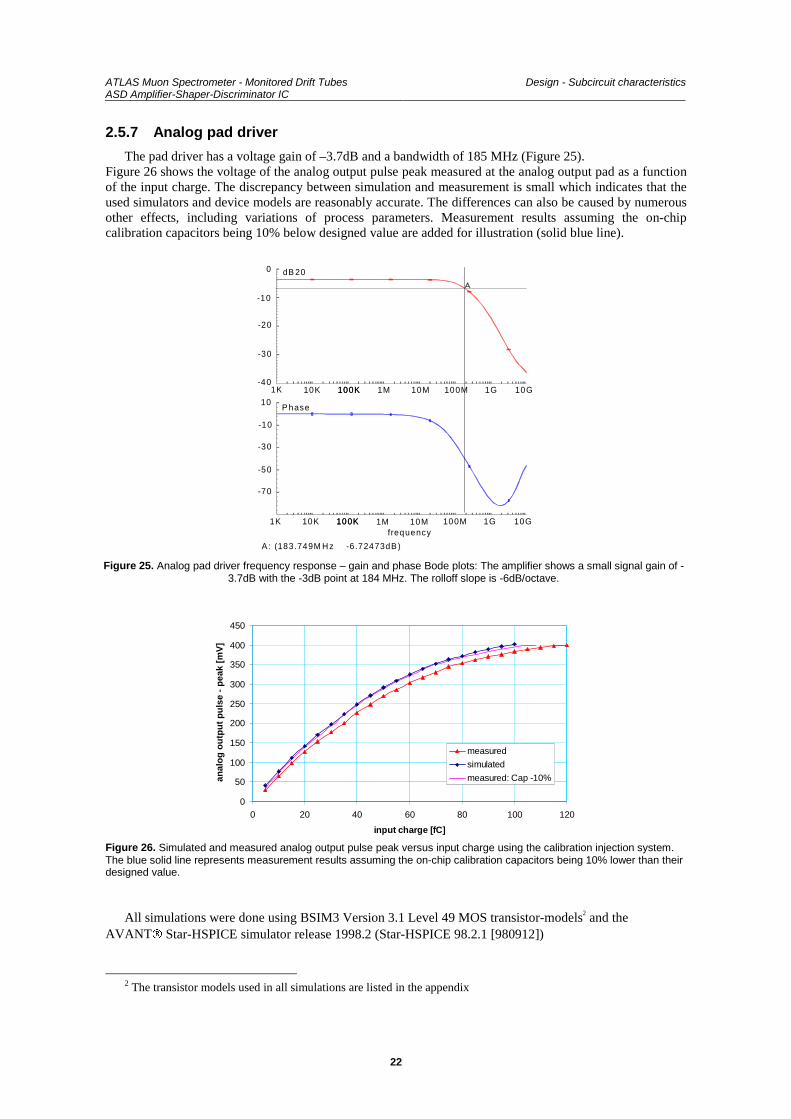
2.5.7 Analog pad driver
The pad driver has a voltage gain of –3.7dB and a bandwidth of 185 MHz (Figure 25).Figure 26 shows the voltage of the analog output pulse peak measured at the analog output pad as a functionof the input charge. The discrepancy between simulation and measurement is small which indicates that theused simulators and device models are reasonably accurate. The differences can also be caused by numerousother effects, including variations of process parameters. Measurement results assuming the on-chipcalibration capacitors being 10% below designed value are added for illustration (solid blue line).
0
-10
-20
-30
-40
10
-10
-30
-50
-70
1K 10K 100K 1M 10M100K 100M 1G 10Gfrequency
A : (183.749M H z -6 .72473dB )
dB 20
P hase
1K 10K 100K 1M 10M100K 100M 1G 10G
Figure 25. Analog pad driver frequency response – gain and phase Bode plots: The amplifier shows a small signal gain of -3.7dB with the -3dB point at 184 MHz. The rolloff slope is -6dB/octave.
0
50
100
150
200
250
300
350
400
450
0 20 40 60 80 100 120
input charge [fC]
anal
og
ou
tpu
t p
uls
e -
pea
k [m
V]
measured
simulated
measured: Cap -10%
Figure 26. Simulated and measured analog output pulse peak versus input charge using the calibration injection system.The blue solid line represents measurement results assuming the on-chip calibration capacitors being 10% lower than theirdesigned value.
All simulations were done using BSIM3 Version 3.1 Level 49 MOS transistor-models2 and theAVANT� Star-HSPICE simulator release 1998.2 (Star-HSPICE 98.2.1 [980912])
2 The transistor models used in all simulations are listed in the appendix
ATLAS Muon Spectrometer - Monitored Drift TubesASD Amplifier-Shaper-Discriminator IC
Design - Programmable parameters
2.6 Programmable parametersIt was found advantageous to be able to control or tune certain analog and functional parameters of the
MDT-ASD, both at power-up/reset and during run time. Rather than applying external currents or voltages,it was chosen to send the control signals as digital data to the chip, where they are converted into physicalquantities by custom Digital-to-Analog Converters (DACs) as required. A serial I/O data interface wasimplemented in the ASD, containing digital I/O ports, shift registers plus shadow registers and the requiredcontrol logic (see 2.6.2 below). The data as well as the control signals and the shift register clock aregenerated by an FPGA3 controller on the mezzanine card and are transmitted to the ASDs using a JTAG likeprotocol.
Table 6 gives a summary of all programmable parameters including their nominal/default settings, range,resolution/LSB and number of bits. The total number of control bits/ASD chip is 53. A power-up/resetroutine, which loads the ASD registers with the nominal values of Table 6 will be incorporated in the JTAGcontroller4.
Table 6. Summary of programmable parameters
Parameter Nominal value Range LSB Units Resolution bitDISC1 Threshold 60 -256 – 256 2 mV 256 8DISC1 Hysteresis 10 0 – 20 1.33 mV 16 4
Wilkinson integration gate 15.333 10 – 50 2.667 ns 16 4DISC2 Threshold 32 32 – 256 32 mV 8 3
Wilkinson discharge current 1.3 1.1 – 2.4 0.1857 PA 8 3Dead-time 800 300 – 1000 100 ns 8 3
Calibration channel mask – – – – – 8Calibration capacitor select – 50 – 400 50 fF 8 3
Channel mode ACTIVE – – – – 16Chip mode ADC – – – – 1
Total number of bits: 53
2.6.1 Programmable analog parameters
2.6.1.1 Timing discriminator threshold
The threshold for the timing discriminator (DISC1) is applied at the AC coupled input of the pre-discriminator differential amplifier (DA-4). As the signal path is fully differential, we use twocomplementary 8-bit dual resistor divider voltage-DACs with an output swing of Vbase ± 128 mV where Vbase
is nominally VDD/2. One of the DACs receives an inverted set of control signals. Consequently the potentialdifference between both DAC outputs, corresponding to the applied threshold, can vary from 256 mVthrough zero to –256 mV. The nominal threshold setting is Vbase ± 30 mV (60 mV effective threshold). Referto [16][17][18] for the determination of optimum threshold levels. Positive and negative reference potentialsare supplied by bootstrap type voltage references.
Table 7 summarizes the main design parameters of the voltage DAC.
Table 7. Main threshold DAC properties
Parameter Definition Value UnitsType VDAC � �
Range VRP � VRN 256 mVResolution N bits 8 �
LSB (VRP � VRN)/2N 1 mVDifferential non-linearity MAX(Vn+1 � Vn) � LSB < 1 mV
Integral non-linearity MAX(Vn � Vn,ideal) < 5 mVMonotonicity Vn d Vn+1 � n �� �
No Missing code Vn z Vn+i � n, i �� �
3 The FPGA may be replaced by an ASIC or the functionality transferred to the TDC (AMT-2).4 It exists also the option to implement this feature on the ASD chip itself.
ATLAS Muon Spectrometer - Monitored Drift TubesASD Amplifier-Shaper-Discriminator IC
Design - Programmable parameters
24
� �
� �
� �
� �
� � � �
� � � � �
� �
� � � � � � � � �
� �
� �
� �
� �
� � � � �
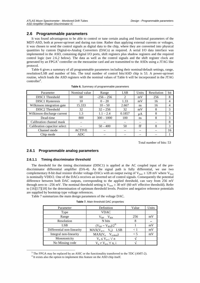
Figure 27. Block schematic of the 8-bit main discriminator threshold voltage DAC
2.6.1.2 Timing discriminator hysteresis
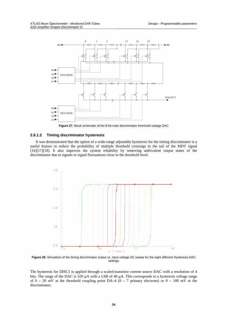
It was demonstrated that the option of a wide-range adjustable hysteresis for the timing discriminator is auseful feature to reduce the probability of multiple threshold crossings in the tail of the MDT signal[16][17][18]. It also improves the system reliability by removing ambivalent output states of thediscriminator due to signals or signal fluctuations close to the threshold level.
Figure 28. Simulation of the timing discriminator output vs. input voltage DC sweep for the eight different Hysteresis-DACsettings
The hysteresis for DISC1 is applied through a scaled-transistor current source DAC with a resolution of 4bits. The range of the DAC is 320 PA with a LSB of 40 PA. This corresponds to a hysteresis voltage rangeof 0 – 20 mV at the threshold coupling point DA–4 (0 – 7 primary electrons) or 0 – 100 mV at thediscriminator.
ATLAS Muon Spectrometer - Monitored Drift TubesASD Amplifier-Shaper-Discriminator IC
Design - Programmable parameters
25
2.6.1.3 Wilkinson ADC Control
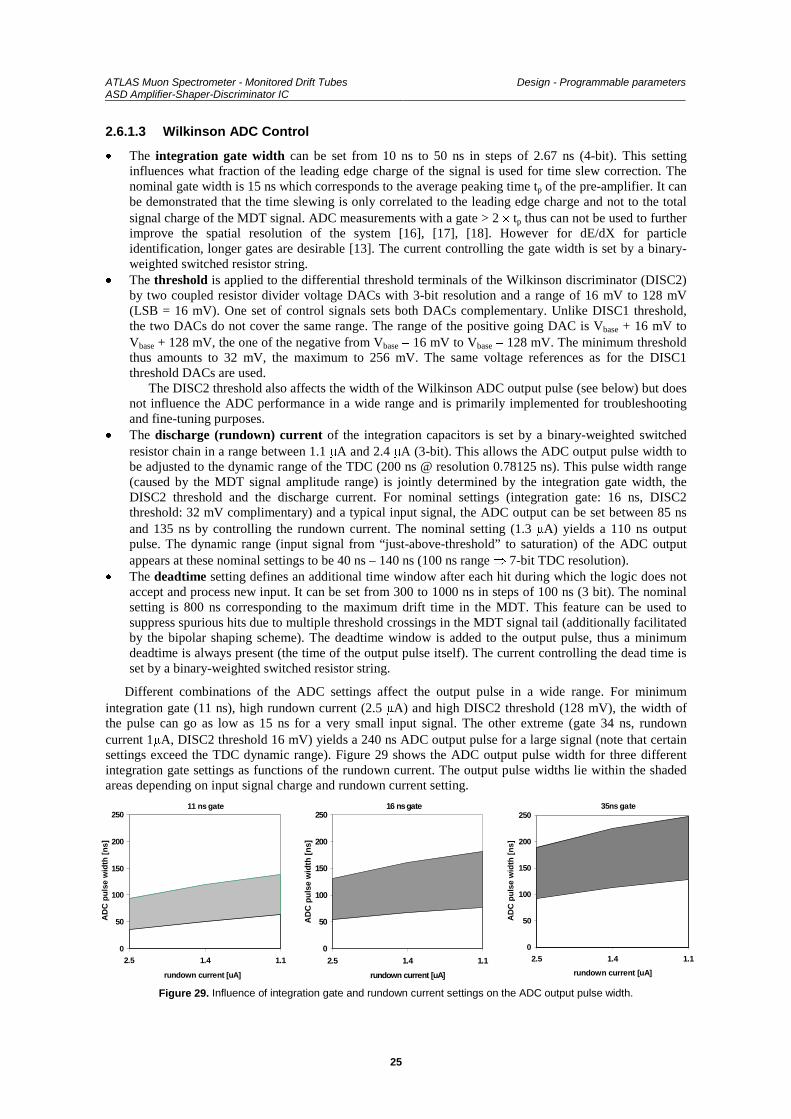
x The integration gate width can be set from 10 ns to 50 ns in steps of 2.67 ns (4-bit). This settinginfluences what fraction of the leading edge charge of the signal is used for time slew correction. Thenominal gate width is 15 ns which corresponds to the average peaking time tp of the pre-amplifier. It canbe demonstrated that the time slewing is only correlated to the leading edge charge and not to the totalsignal charge of the MDT signal. ADC measurements with a gate > 2 u tp thus can not be used to furtherimprove the spatial resolution of the system [16], [17], [18]. However for dE/dX for particleidentification, longer gates are desirable [13]. The current controlling the gate width is set by a binary-weighted switched resistor string.
x The threshold is applied to the differential threshold terminals of the Wilkinson discriminator (DISC2)by two coupled resistor divider voltage DACs with 3-bit resolution and a range of 16 mV to 128 mV(LSB = 16 mV). One set of control signals sets both DACs complementary. Unlike DISC1 threshold,the two DACs do not cover the same range. The range of the positive going DAC is Vbase + 16 mV toVbase + 128 mV, the one of the negative from Vbase � 16 mV to Vbase � 128 mV. The minimum thresholdthus amounts to 32 mV, the maximum to 256 mV. The same voltage references as for the DISC1threshold DACs are used.
The DISC2 threshold also affects the width of the Wilkinson ADC output pulse (see below) but doesnot influence the ADC performance in a wide range and is primarily implemented for troubleshootingand fine-tuning purposes.
x The discharge (rundown) current of the integration capacitors is set by a binary-weighted switchedresistor chain in a range between 1.1 PA and 2.4 PA (3-bit). This allows the ADC output pulse width tobe adjusted to the dynamic range of the TDC (200 ns @ resolution 0.78125 ns). This pulse width range(caused by the MDT signal amplitude range) is jointly determined by the integration gate width, theDISC2 threshold and the discharge current. For nominal settings (integration gate: 16 ns, DISC2threshold: 32 mV complimentary) and a typical input signal, the ADC output can be set between 85 nsand 135 ns by controlling the rundown current. The nominal setting (1.3 PA) yields a 110 ns outputpulse. The dynamic range (input signal from “just-above-threshold” to saturation) of the ADC outputappears at these nominal settings to be 40 ns – 140 ns (100 ns range � 7-bit TDC resolution).
x The deadtime setting defines an additional time window after each hit during which the logic does notaccept and process new input. It can be set from 300 to 1000 ns in steps of 100 ns (3 bit). The nominalsetting is 800 ns corresponding to the maximum drift time in the MDT. This feature can be used tosuppress spurious hits due to multiple threshold crossings in the MDT signal tail (additionally facilitatedby the bipolar shaping scheme). The deadtime window is added to the output pulse, thus a minimumdeadtime is always present (the time of the output pulse itself). The current controlling the dead time isset by a binary-weighted switched resistor string.
Different combinations of the ADC settings affect the output pulse in a wide range. For minimumintegration gate (11 ns), high rundown current (2.5 PA) and high DISC2 threshold (128 mV), the width ofthe pulse can go as low as 15 ns for a very small input signal. The other extreme (gate 34 ns, rundowncurrent 1PA, DISC2 threshold 16 mV) yields a 240 ns ADC output pulse for a large signal (note that certainsettings exceed the TDC dynamic range). Figure 29 shows the ADC output pulse width for three differentintegration gate settings as functions of the rundown current. The output pulse widths lie within the shadedareas depending on input signal charge and rundown current setting.
11 ns gate
0
50
100
150
200
250
2.5 1.4 1.1
rundown current [uA]
AD
C p
uls
e w
idth
[n
s]
16 ns gate
0
50
100
150
200
250
2.5 1.4 1.1
rundown current [uA]
AD
C p
uls
e w
idth
[n
s]
35ns gate
0
50
100
150
200
250
2.5 1.4 1.1
rundown current [uA]
AD
C p
uls
e w
idth
[n
s]
Figure 29. Influence of integration gate and rundown current settings on the ADC output pulse width.
ATLAS Muon Spectrometer - Monitored Drift TubesASD Amplifier-Shaper-Discriminator IC
Design - Programmable parameters
26
2.6.2 Programmable functional parameters
2.6.2.1 Calibration/test pulse injection
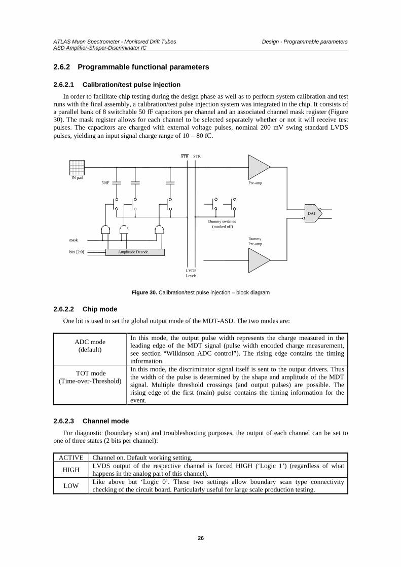
In order to facilitate chip testing during the design phase as well as to perform system calibration and testruns with the final assembly, a calibration/test pulse injection system was integrated in the chip. It consists ofa parallel bank of 8 switchable 50 fF capacitors per channel and an associated channel mask register (Figure30). The mask register allows for each channel to be selected separately whether or not it will receive testpulses. The capacitors are charged with external voltage pulses, nominal 200 mV swing standard LVDSpulses, yielding an input signal charge range of 10 � 80 fC.
50fFIN pad
Amplitude Decode
STR STR
LVDSLevels
bits [2:0]
mask
Dummy switches (masked off)
Pre-amp
DummyPre-amp
DA1
Figure 30. Calibration/test pulse injection – block diagram
2.6.2.2 Chip mode
One bit is used to set the global output mode of the MDT-ASD. The two modes are:
ADC mode(default)
In this mode, the output pulse width represents the charge measured in theleading edge of the MDT signal (pulse width encoded charge measurement,see section “Wilkinson ADC control”). The rising edge contains the timinginformation.
TOT mode(Time-over-Threshold)
In this mode, the discriminator signal itself is sent to the output drivers. Thusthe width of the pulse is determined by the shape and amplitude of the MDTsignal. Multiple threshold crossings (and output pulses) are possible. Therising edge of the first (main) pulse contains the timing information for theevent.
2.6.2.3 Channel mode
For diagnostic (boundary scan) and troubleshooting purposes, the output of each channel can be set toone of three states (2 bits per channel):
ACTIVE Channel on. Default working setting.
HIGHLVDS output of the respective channel is forced HIGH (‘Logic 1’) (regardless of whathappens in the analog part of this channel).
LOWLike above but ‘Logic 0’. These two settings allow boundary scan type connectivitychecking of the circuit board. Particularly useful for large scale production testing.
ATLAS Muon Spectrometer - Monitored Drift TubesASD Amplifier-Shaper-Discriminator IC
Design - Serial data interface
27
2.7 Serial data interface
2.7.1 Architecture
The chosen ASD serial data interface architecture employs separate shift and working registers. The shiftregister is connected directly to digital input and output pads respectively. Its length is designed to hold acomplete set of control bits (53). The data can be uploaded any time (asynchronously) to the shadowregisters, which control the DACs, multiplexers etc. The architecture allows downloading the whole set ofactive bits from the shadow to the shift register in order to send them back to the controller for diagnostic ormonitoring purposes. This can be done any time and does not interfere with the normal operation of theASD. The interface, for each data bit, consists of the shift register-cell, implemented as a static master-slaveD flip-flop, the shadow register cell, realized as a static transparent latch and 2 two-in-one multiplexers(Figure 31). ASDs thus can be daisy-chained to form a closed JTAG type control loop.
Figure 31. Serial data interface
2.7.2 I/O operation
The protocol requires 2 data lines (TO and FROM chip), 3 control lines (SHIFT [D0], DOWN [D1],LOAD [D2]) and one clock line (Table 8). The configuration allows extensive control over the data flow(Table 9). HOLD mode keeps the data in the shift register by feeding back each cell with its own content.SHIFT mode shifts data right at the rising edge of the clock. LOAD active copies the bits in the shift registerto the shadow register at any time (asynchronous). DOWN active copies the contents of the shadow registersto the shift register at the next rising clock edge (overrides SHIFT � HOLD). The ASD serial input expectsthe data to be stable at the rising edge of the clock r a few nanoseconds. The controller will change data bitsat the falling clock-edge. Thus data are stable at the input for the entire clock period with the sensitive risingedge in the middle. Data bits at the ASD serial data output also change state at the falling edge of the clock.
D Q
CLK
1
0
Q
1
0
Q
LOAD
D Q TO DAC
TO NEXT CELL
S
SFROM PREVIOUS CELL
D0: SHIFT
D1: DOWN
SHIFT CELL
SHADOW CELLD2: LOAD
ATLAS Muon Spectrometer - Monitored Drift TubesASD Amplifier-Shaper-Discriminator IC
Design - Serial data interface
28
Table 8. Serial interface signal lines
DATA_IN Data line from controller to ASD shift register inputDATA_OUT Data line from ASD shift register output to controller
CLK Clock lineD[0:2] Register control lines
Table 9. Serial interface instruction encoding
Instruction D0 D1 D2 OperationSHIFT 1 0 X Shift right at rising edge of CLKHOLD 0 0 X Keep shift register contents (self feedback)DOWN X 1 X Copy contents of shadow register to shift register @ rising edge of CLKLOAD X X 1 Load shadow registers with contents of shift register (asynchronous)
Shift and shadow registers have a length of 54 bits, where 53 are actual data bits. The last shift registercell is clocked with an inverted clock, making the output change at the falling edge of the clock. A DOWNinstruction causes the last cell to perform a HOLD operation.
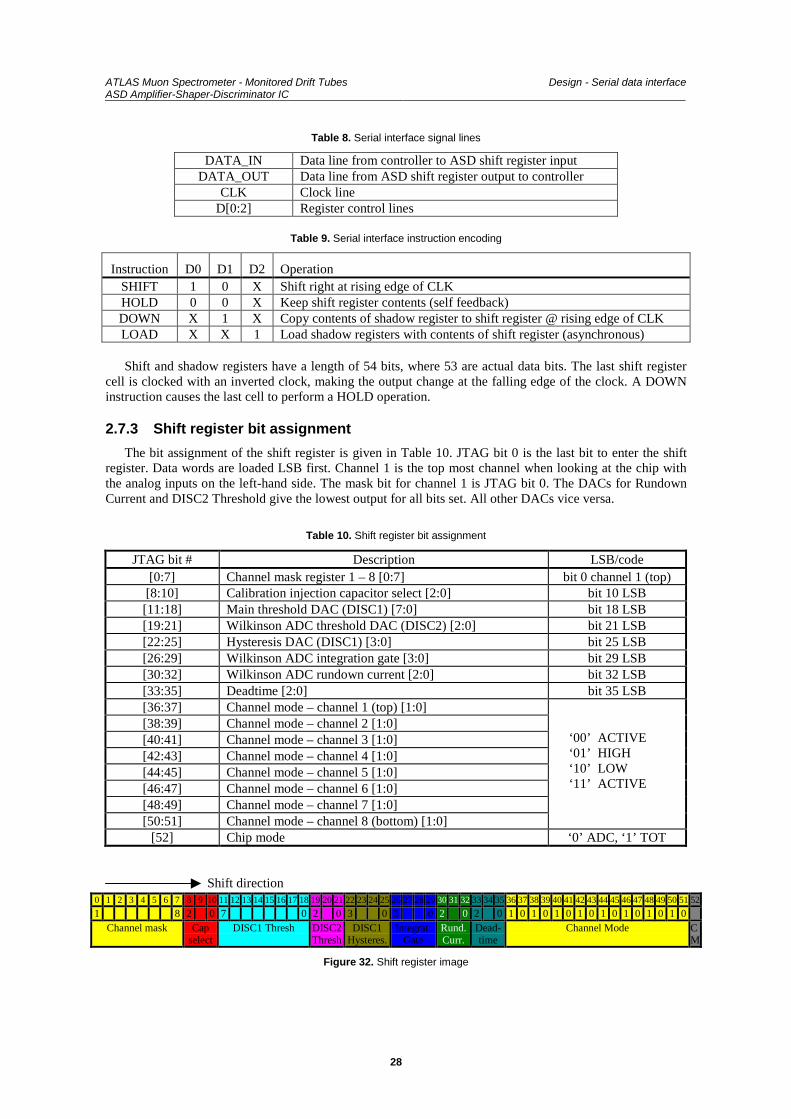
2.7.3 Shift register bit assignment
The bit assignment of the shift register is given in Table 10. JTAG bit 0 is the last bit to enter the shiftregister. Data words are loaded LSB first. Channel 1 is the top most channel when looking at the chip withthe analog inputs on the left-hand side. The mask bit for channel 1 is JTAG bit 0. The DACs for RundownCurrent and DISC2 Threshold give the lowest output for all bits set. All other DACs vice versa.
Table 10. Shift register bit assignment
JTAG bit # Description LSB/code[0:7] Channel mask register 1 – 8 [0:7] bit 0 channel 1 (top)
[8:10] Calibration injection capacitor select [2:0] bit 10 LSB[11:18] Main threshold DAC (DISC1) [7:0] bit 18 LSB[19:21] Wilkinson ADC threshold DAC (DISC2) [2:0] bit 21 LSB[22:25] Hysteresis DAC (DISC1) [3:0] bit 25 LSB[26:29] Wilkinson ADC integration gate [3:0] bit 29 LSB[30:32] Wilkinson ADC rundown current [2:0] bit 32 LSB[33:35] Deadtime [2:0] bit 35 LSB[36:37] Channel mode – channel 1 (top) [1:0][38:39] Channel mode – channel 2 [1:0][40:41] Channel mode – channel 3 [1:0][42:43] Channel mode – channel 4 [1:0][44:45] Channel mode – channel 5 [1:0][46:47] Channel mode – channel 6 [1:0][48:49] Channel mode – channel 7 [1:0][50:51] Channel mode – channel 8 (bottom) [1:0]
‘00’ ACTIVE ‘01’ HIGH ‘10’ LOW ‘11’ ACTIVE
[52] Chip mode ‘0’ ADC, ‘1’ TOT
0 1 2 3 4 5 6 7 8 9 10 11 12 13 14 15 16 17 18 19 20 21 22 23 24 25 26 27 28 29 30 31 32 33 34 35 36 37 38 39 40 41 42 43 44 45 46 47 48 49 50 51 52
1 8 2 0 7 0 2 0 3 0 3 0 2 0 2 0 1 0 1 0 1 0 1 0 1 0 1 0 1 0 1 0Channel mask Cap
selectDISC1 Thresh DISC2
ThreshDISC1
Hysteres.Integrat.
GateRund.Curr.
Dead-time
Channel Mode CM
Figure 32. Shift register image
Shift direction
ATLAS Muon Spectrometer - Monitored Drift TubesASD Amplifier-Shaper-Discriminator IC
Design - IC layout
29
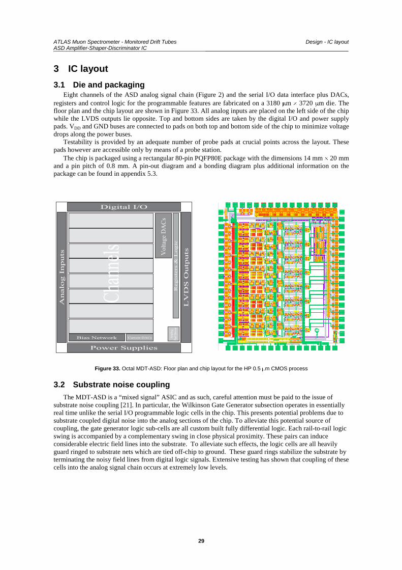
3 IC layout
3.1 Die and packagingEight channels of the ASD analog signal chain (Figure 2) and the serial I/O data interface plus DACs,
registers and control logic for the programmable features are fabricated on a 3180 Pm u 3720 Pm die. Thefloor plan and the chip layout are shown in Figure 33. All analog inputs are placed on the left side of the chipwhile the LVDS outputs lie opposite. Top and bottom sides are taken by the digital I/O and power supplypads. VDD and GND buses are connected to pads on both top and bottom side of the chip to minimize voltagedrops along the power buses.
Testability is provided by an adequate number of probe pads at crucial points across the layout. Thesepads however are accessible only by means of a probe station.
The chip is packaged using a rectangular 80-pin PQFP80E package with the dimensions 14 mm u 20 mmand a pin pitch of 0.8 mm. A pin-out diagram and a bonding diagram plus additional information on thepackage can be found in appendix 5.3.
�������������
� �!�������
� " � " � � � � � #
� � $ % & � ! � � � � " % �
%�"��%&��'
����"(
�����%�����
) " � � � � % � $ � & * � � & & % � � � � � � �
����������
��+��&",%&
�-���%��
Figure 33. Octal MDT-ASD: Floor plan and chip layout for the HP 0.5 Pm CMOS process
3.2 Substrate noise couplingThe MDT-ASD is a “mixed signal” ASIC and as such, careful attention must be paid to the issue of
substrate noise coupling [21]. In particular, the Wilkinson Gate Generator subsection operates in essentiallyreal time unlike the serial I/O programmable logic cells in the chip. This presents potential problems due tosubstrate coupled digital noise into the analog sections of the chip. To alleviate this potential source ofcoupling, the gate generator logic sub-cells are all custom built fully differential logic. Each rail-to-rail logicswing is accompanied by a complementary swing in close physical proximity. These pairs can induceconsiderable electric field lines into the substrate. To alleviate such effects, the logic cells are all heavilyguard ringed to substrate nets which are tied off-chip to ground. These guard rings stabilize the substrate byterminating the noisy field lines from digital logic signals. Extensive testing has shown that coupling of thesecells into the analog signal chain occurs at extremely low levels.
ATLAS Muon Spectrometer - Monitored Drift TubesASD Amplifier-Shaper-Discriminator IC
Prototyping - Test and measurement results
4 Prototyping - test and measurement resultsAll sub-circuits and building blocks of the MDT-ASD were prototyped at different stages of the
development. One of the prototypes, dubbed “ASD light”, a reduced-functionality5 4-channel chip wasproduced in larger quantities to be used for MDT chamber production testing. The following sectionscontain test and measurement results taken from different prototype chips, but mainly from the final octalprototype ASD00A. All results are produced by the final sub-circuit versions as implemented on ASD00Aand intended to be identical on the production version of the chip.
4.1 Sub-circuits and building blocks
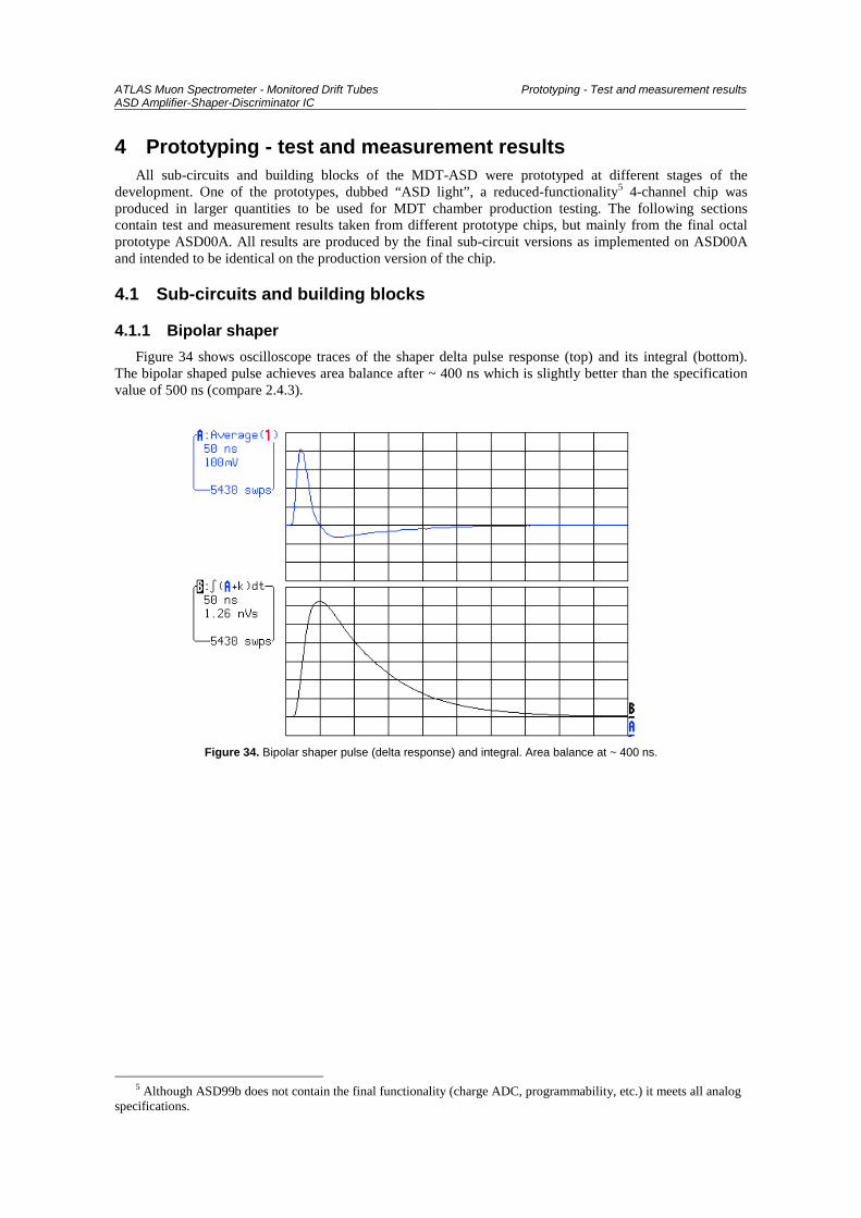
4.1.1 Bipolar shaper
Figure 34 shows oscilloscope traces of the shaper delta pulse response (top) and its integral (bottom).The bipolar shaped pulse achieves area balance after ~ 400 ns which is slightly better than the specificationvalue of 500 ns (compare 2.4.3).
Figure 34. Bipolar shaper pulse (delta response) and integral. Area balance at ~ 400 ns.
5 Although ASD99b does not contain the final functionality (charge ADC, programmability, etc.) it meets all analog
specifications.
ATLAS Muon Spectrometer - Monitored Drift TubesASD Amplifier-Shaper-Discriminator IC
Prototyping - Test and measurement results
31
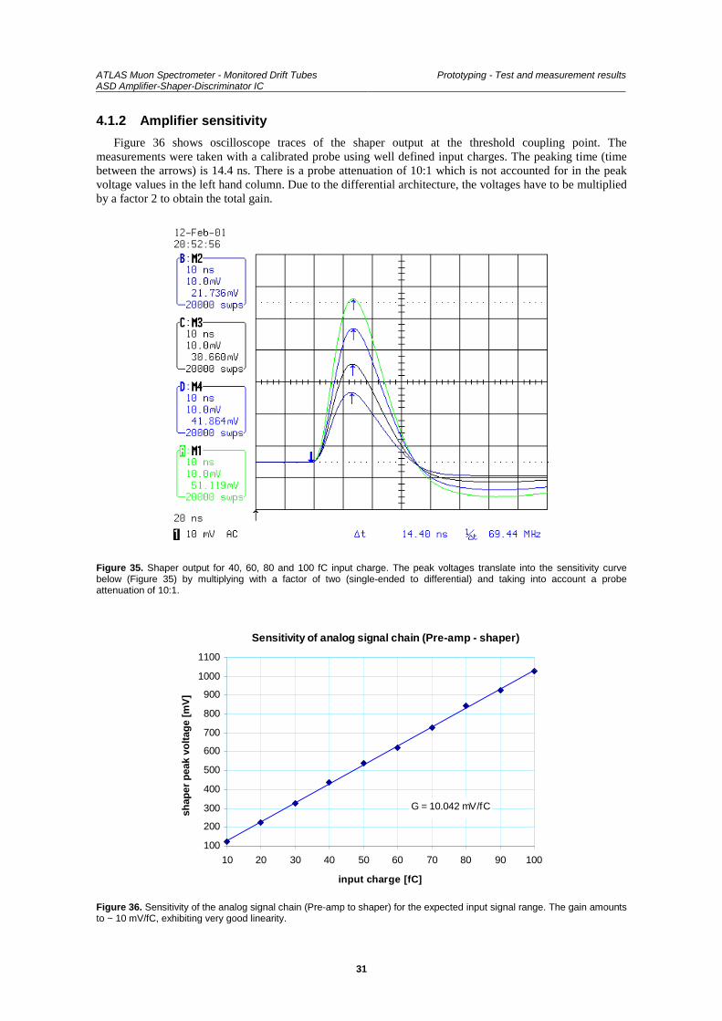
4.1.2 Amplifier sensitivity
Figure 36 shows oscilloscope traces of the shaper output at the threshold coupling point. Themeasurements were taken with a calibrated probe using well defined input charges. The peaking time (timebetween the arrows) is 14.4 ns. There is a probe attenuation of 10:1 which is not accounted for in the peakvoltage values in the left hand column. Due to the differential architecture, the voltages have to be multipliedby a factor 2 to obtain the total gain.
Figure 35. Shaper output for 40, 60, 80 and 100 fC input charge. The peak voltages translate into the sensitivity curvebelow (Figure 35) by multiplying with a factor of two (single-ended to differential) and taking into account a probeattenuation of 10:1.
Sensitivity of analog signal chain (Pre-amp - shaper)
G = 10.042 mV/fC
100
200
300
400
500
600
700
800
900
1000
1100
10 20 30 40 50 60 70 80 90 100
input charge [fC]
shap
er p
eak
volt
age
[mV
]
Figure 36. Sensitivity of the analog signal chain (Pre-amp to shaper) for the expected input signal range. The gain amountsto ~ 10 mV/fC, exhibiting very good linearity.
ATLAS Muon Spectrometer - Monitored Drift TubesASD Amplifier-Shaper-Discriminator IC
Prototyping - Test and measurement results
32
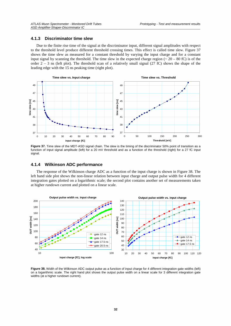
4.1.3 Discriminator time slew
Due to the finite rise time of the signal at the discriminator input, different signal amplitudes with respectto the threshold level produce different threshold crossing times. This effect is called time slew. Figure 37shows the time slew as measured for a constant threshold by varying the input charge and for a constantinput signal by scanning the threshold. The time slew in the expected charge region (~ 20 – 80 fC) is of theorder 2 – 3 ns (left plot). The threshold scan of a relatively small signal (27 fC) shows the shape of theleading edge with the 15 ns peaking time (right plot).
Time slew vs. Input charge
37
39
41
43
45
47
49
0 10 20 30 40 50 60 70 80 90
input charge [fC]
tim
e sl
ew [
ns]
Time slew vs. Threshold
37
39
41
43
45
47
49
0 50 100 150 200 250 300
Threshold [mV]
tim
e sl
ew [
ns]
Figure 37. Time slew of the MDT-ASD signal chain. The slew is the timing of the discriminator 50% point of transition as afunction of input signal amplitude (left) for a 20 mV threshold and as a function of the threshold (right) for a 27 fC inputsignal.
4.1.4 Wilkinson ADC performance
The response of the Wilkinson charge ADC as a function of the input charge is shown in Figure 38. Theleft hand side plot shows the non-linear relation between input charge and output pulse width for 4 differentintegration gates plotted on a logarithmic scale; the second plot contains another set of measurements takenat higher rundown current and plotted on a linear scale.
Output pulse width vs. input charge
40
60
80
100
120
140
160
180
200
10 100
input charge [fC], log scale
OU
T w
idth
[n
s]
gate 12 ns
gate 14 ns
gate 17.5 ns
gate 20.5 ns
Output pulse width vs. input charge
30
40
50
60
70
80
90
100
110
120
130
140
10 20 30 40 50 60 70 80 90 100 110 120
input charge [fC]
OU
T w
idth
[n
s]
gate 12 nsgate 14 nsgate 17.5 ns
Figure 38. Width of the Wilkinson ADC output pulse as a function of input charge for 4 different integration gate widths (left)on a logarithmic scale. The right hand plot shows the output pulse width on a linear scale for 3 different integration gatewidths (at a higher rundown current).
ATLAS Muon Spectrometer - Monitored Drift TubesASD Amplifier-Shaper-Discriminator IC
Prototyping - Test and measurement results
33
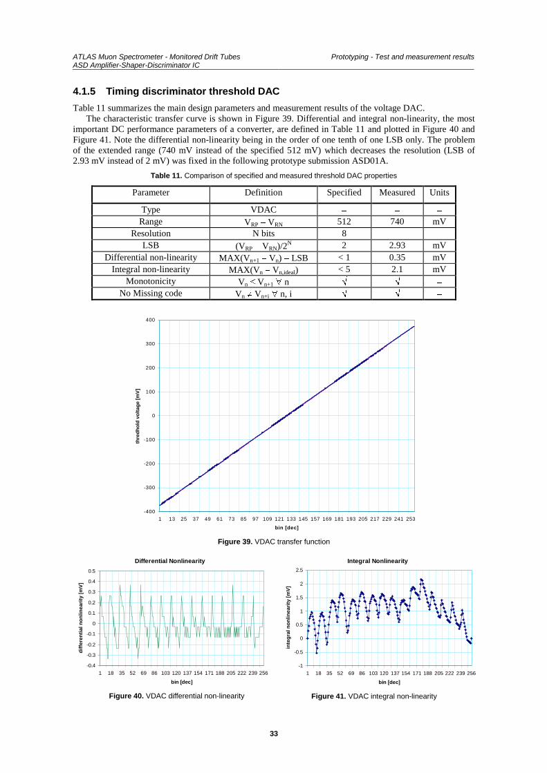
4.1.5 Timing discriminator threshold DAC
Table 11 summarizes the main design parameters and measurement results of the voltage DAC.The characteristic transfer curve is shown in Figure 39. Differential and integral non-linearity, the most
important DC performance parameters of a converter, are defined in Table 11 and plotted in Figure 40 andFigure 41. Note the differential non-linearity being in the order of one tenth of one LSB only. The problemof the extended range (740 mV instead of the specified 512 mV) which decreases the resolution (LSB of2.93 mV instead of 2 mV) was fixed in the following prototype submission ASD01A.
Table 11. Comparison of specified and measured threshold DAC properties
Parameter Definition Specified Measured Units
Type VDAC � � �
Range VRP � VRN 512 740 mVResolution N bits 8 � �
LSB (VRP � VRN)/2N 2 2.93 mVDifferential non-linearity MAX(Vn+1 � Vn) � LSB < 1 0.35 mV
Integral non-linearity MAX(Vn � Vn,ideal) < 5 2.1 mVMonotonicity Vn d Vn+1 � n �� �� �
No Missing code Vn z Vn+i � n, i �� �� �
-400
-300
-200
-100
0
100
200
300
400
1 13 25 37 49 61 73 85 97 109 121 133 145 157 169 181 193 205 217 229 241 253
bin [dec]
thre
dh
old
vo
ltag
e [m
V]
Figure 39. VDAC transfer function
Differential Nonlinearity
-0.4
-0.3
-0.2
-0.1
0
0.1
0.2
0.3
0.4
0.5
1 18 35 52 69 86 103 120 137 154 171 188 205 222 239 256
bin [dec]
dif
fere
nti
al n
on
linea
rity
[m
V]
Figure 40. VDAC differential non-linearity
Integral Nonlinearity
-1
-0.5
0
0.5
1
1.5
2
2.5
1 18 35 52 69 86 103 120 137 154 171 188 205 222 239 256
bin [dec]
inte
gra
l no
nlin
eari
ty [
mV
]
Figure 41. VDAC integral non-linearity
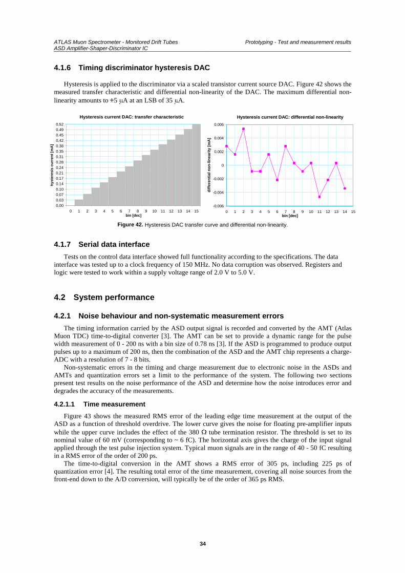
ATLAS Muon Spectrometer - Monitored Drift TubesASD Amplifier-Shaper-Discriminator IC
Prototyping - Test and measurement results
34
4.1.6 Timing discriminator hysteresis DAC
Hysteresis is applied to the discriminator via a scaled transistor current source DAC. Figure 42 shows themeasured transfer characteristic and differential non-linearity of the DAC. The maximum differential non-linearity amounts to r5 PA at an LSB of 35 PA.
Hysteresis current DAC: transfer characteristic
0.000.030.070.100.140.170.210.240.280.310.350.380.420.450.490.52
0 1 2 3 4 5 6 7 8 9 10 11 12 13 14 15bin [dec]
hys
tere
sis
curr
ent
[mA
]
Hysteresis current DAC: differential non-linearity
-0.006
-0.004
-0.002
0
0.002
0.004
0.006
0 1 2 3 4 5 6 7 8 9 10 11 12 13 14 15bin [dec]
dif
fere
nti
al n
on
-lin
eari
ty [
mA
]
Figure 42. Hysteresis DAC transfer curve and differential non-linearity.
4.1.7 Serial data interface
Tests on the control data interface showed full functionality according to the specifications. The datainterface was tested up to a clock frequency of 150 MHz. No data corruption was observed. Registers andlogic were tested to work within a supply voltage range of 2.0 V to 5.0 V.
4.2 System performance
4.2.1 Noise behaviour and non-systematic measurement errors
The timing information carried by the ASD output signal is recorded and converted by the AMT (AtlasMuon TDC) time-to-digital converter [3]. The AMT can be set to provide a dynamic range for the pulsewidth measurement of 0 - 200 ns with a bin size of 0.78 ns [3]. If the ASD is programmed to produce outputpulses up to a maximum of 200 ns, then the combination of the ASD and the AMT chip represents a charge-ADC with a resolution of 7 - 8 bits.
Non-systematic errors in the timing and charge measurement due to electronic noise in the ASDs andAMTs and quantization errors set a limit to the performance of the system. The following two sectionspresent test results on the noise performance of the ASD and determine how the noise introduces error anddegrades the accuracy of the measurements.
4.2.1.1 Time measurement
Figure 43 shows the measured RMS error of the leading edge time measurement at the output of theASD as a function of threshold overdrive. The lower curve gives the noise for floating pre-amplifier inputswhile the upper curve includes the effect of the 380 : tube termination resistor. The threshold is set to itsnominal value of 60 mV (corresponding to ~ 6 fC). The horizontal axis gives the charge of the input signalapplied through the test pulse injection system. Typical muon signals are in the range of 40 - 50 fC resultingin a RMS error of the order of 200 ps.
The time-to-digital conversion in the AMT shows a RMS error of 305 ps, including 225 ps ofquantization error [4]. The resulting total error of the time measurement, covering all noise sources from thefront-end down to the A/D conversion, will typically be of the order of 365 ps RMS.
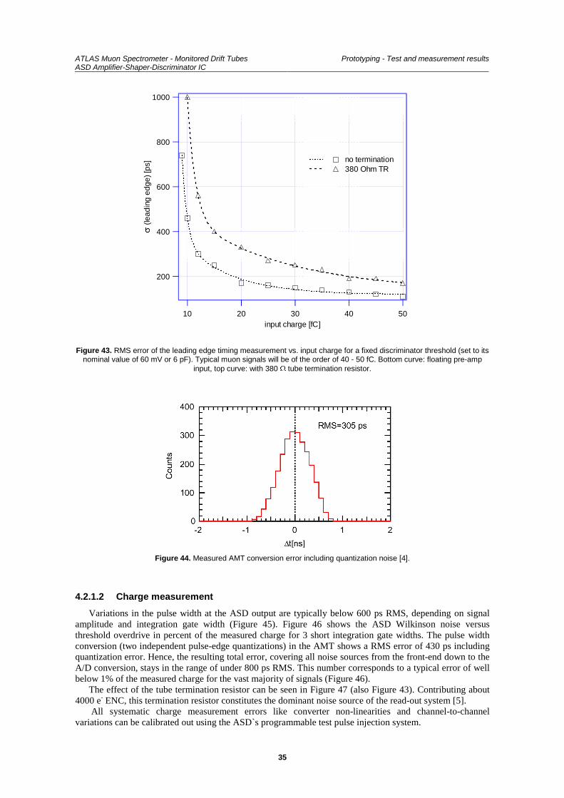
ATLAS Muon Spectrometer - Monitored Drift TubesASD Amplifier-Shaper-Discriminator IC
Prototyping - Test and measurement results
35
1000
800
600
400
200
V (l
eadi
ng e
dge)
[ps]
5040302010input charge [fC]
no termination380 Ohm TR
Figure 43. RMS error of the leading edge timing measurement vs. input charge for a fixed discriminator threshold (set to itsnominal value of 60 mV or 6 pF). Typical muon signals will be of the order of 40 - 50 fC. Bottom curve: floating pre-amp
input, top curve: with 380 : tube termination resistor.
Figure 44. Measured AMT conversion error including quantization noise [4].
4.2.1.2 Charge measurement
Variations in the pulse width at the ASD output are typically below 600 ps RMS, depending on signalamplitude and integration gate width (Figure 45). Figure 46 shows the ASD Wilkinson noise versusthreshold overdrive in percent of the measured charge for 3 short integration gate widths. The pulse widthconversion (two independent pulse-edge quantizations) in the AMT shows a RMS error of 430 ps includingquantization error. Hence, the resulting total error, covering all noise sources from the front-end down to theA/D conversion, stays in the range of under 800 ps RMS. This number corresponds to a typical error of wellbelow 1% of the measured charge for the vast majority of signals (Figure 46).
The effect of the tube termination resistor can be seen in Figure 47 (also Figure 43). Contributing about4000 e- ENC, this termination resistor constitutes the dominant noise source of the read-out system [5].
All systematic charge measurement errors like converter non-linearities and channel-to-channelvariations can be calibrated out using the ASD`s programmable test pulse injection system.
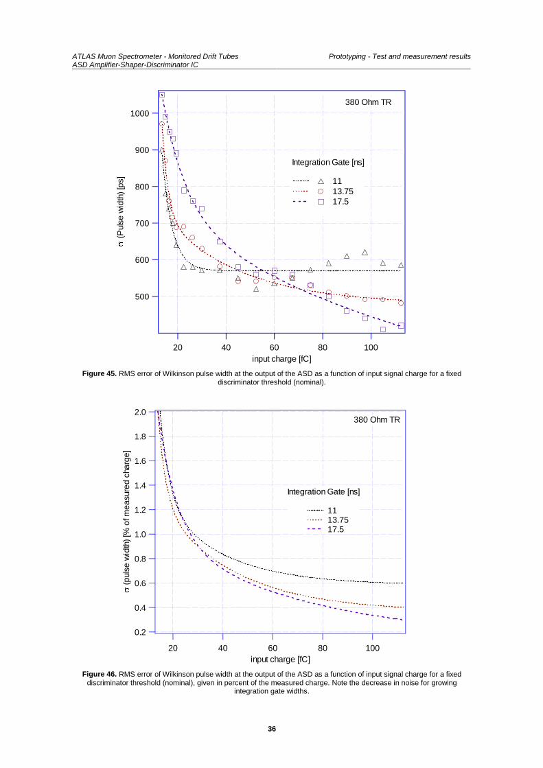
ATLAS Muon Spectrometer - Monitored Drift TubesASD Amplifier-Shaper-Discriminator IC
Prototyping - Test and measurement results
36
1000
900
800
700
600
500
V(P
ulse
wid
th) [
ps]
10080604020input charge [fC]
Integration Gate [ns]
11 13.75 17.5
380 Ohm TR
Figure 45. RMS error of Wilkinson pulse width at the output of the ASD as a function of input signal charge for a fixeddiscriminator threshold (nominal).
2.0
1.8
1.6
1.4
1.2
1.0
0.8
0.6
0.4
0.2
V (p
ulse
wid
th) [
% o
f mea
sure
d ch
arge
]
10080604020input charge [fC]
Integration Gate [ns] 11 13.75 17.5
380 Ohm TR
Figure 46. RMS error of Wilkinson pulse width at the output of the ASD as a function of input signal charge for a fixeddiscriminator threshold (nominal), given in percent of the measured charge. Note the decrease in noise for growing
integration gate widths.
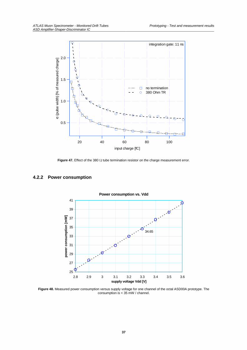
ATLAS Muon Spectrometer - Monitored Drift TubesASD Amplifier-Shaper-Discriminator IC
Prototyping - Test and measurement results
37
2.0
1.5
1.0
0.5
V (p
ulse
wid
th) [
% o
f mea
sure
d ch
arge
]
10080604020
input charge [fC]
no termination 380 Ohm TR
integration gate: 11 ns
Figure 47. Effect of the 380 : tube termination resistor on the charge measurement error.
4.2.2 Power consumption
Power consumption vs. Vdd
34.65
25
27
29
31
33
35
37
39
41
2.8 2.9 3 3.1 3.2 3.3 3.4 3.5 3.6supply voltage Vdd [V]
po
wer
co
nsu
mp
tio
n [
mW
]
Figure 48. Measured power consumption versus supply voltage for one channel of the octal ASD00A prototype. Theconsumption is < 35 mW / channel.
ATLAS Muon Spectrometer - Monitored Drift TubesASD Amplifier-Shaper-Discriminator IC
Appendix - MOS transistor models
5 Appendix
5.1 MOS transistor models
.MODEL CMOSN NMOS LEVEL = 49+VERSION = 3.1 TNOM = 27 TOX = 9.6E-9+XJ = 1.5E-7 NCH = 1.7E17 VTH0 = 0.6607278+K1 = 0.7328155 K2 = -0.0164557 K3 = 37.6307825+K3B = -0.6826036 W0 = 5.954482E-6 NLX = 1.160795E-8+DVT0W = 0 DVT1W = 0 DVT2W = 0+DVT0 = 5.9023096 DVT1 = 1.0356475 DVT2 = -0.1928577+U0 = 494.1066594 UA = 5.793483E-10 UB = 1.282667E-18+UC = 3.434774E-11 VSAT = 1.259976E5 A0 = 0.9390877+AGS = 0.1848153 B0 = 2.222029E-6 B1 = 5E-6+KETA = -1.711114E-3 A1 = 0 A2 = 1+RDSW = 1.640042E3 PRWG = -0.0418215 PRWB = -0.0750653+WR = 1 WINT = 2.612312E-7 LINT = 1.114883E-7+XL = -1E-7 XW = 0 DWG = -1.070966E-8+DWB = 1.235807E-8 VOFF = -0.0896698 NFACTOR = 1.2143784+CIT = 0 CDSC = 1.171765E-4 CDSCD = 1E-3+CDSCB = 2.979369E-5 ETA0 = 1.712692E-3 ETAB = 3.4153E-3+DSUB = 0.7387012 PCLM = 0.6279545 PDIBLC1 = 0.0416968+PDIBLC2 = 3.027171E-3 PDIBLCB = -0.1 DROUT = 0.4026747+PSCBE1 = 3.664597E10 PSCBE2 = 1.6701E-8 PVAG = 0.1613363+DELTA = 0.01 MOBMOD = 1 PRT = 0+UTE = -1.5 KT1 = -0.11 KT1L = 0+KT2 = 0.022 UA1 = 4.31E-9 UB1 = -7.61E-18+UC1 = -5.6E-11 AT = 3.3E4 WL = 0+WLN = 1 WW = -1.245E-15 WWN = 1.125+WWL = 0 LL = 0 LLN = 1+LW = 0 LWN = 1 LWL = 0+CAPMOD = 2 XPART = 0.4 CGDO = 2.51E-10+CGSO = 2.51E-10 CGBO = 1E-11 CJ = 5.06534E-4+PB = 0.99 MJ = 0.7315511 CJSW = 4.076138E-10+PBSW = 0.99 MJSW = 0.1 PVTH0 = 3.611855E-4+PRDSW = -47.8578499 PK2 = 8.209074E-3 WKETA = -5.880416E-3+LKETA = 1.690549E-3 PAGS = 0.0968*
.MODEL CMOSP PMOS LEVEL = 49+VERSION = 3.1 TNOM = 27 TOX = 9.6E-9+XJ = 1.5E-7 NCH = 1.7E17 VTH0 = -0.8451175+K1 = 0.374455 K2 = 0.0214736 K3 = 44.5726978+K3B = -1.4496401 W0 = 5.256776E-6 NLX = 8.640935E-8+DVT0W = 0 DVT1W = 0 DVT2W = 0+DVT0 = 3.8393012 DVT1 = 0.6051434 DVT2 = -0.0821732+U0 = 179.9725329 UA = 1.189439E-9 UB = 1.189025E-18+UC = -5.01386E-11 VSAT = 1.831276E5 A0 = 0.6676752+AGS = 0.325462 B0 = 5.720667E-6 B1 = 5E-6+KETA = 9.806091E-4 A1 = 0 A2 = 1+RDSW = 2.476373E3 PRWG = -0.0212227 PRWB = -0.0823133+WR = 1 WINT = 2.441032E-7 LINT = 4.330033E-8+XL = -1E-7 XW = 0 DWG = -2.061704E-8+DWB = 1.11758E-8 VOFF = -0.0956807 NFACTOR = 0.9637884+CIT = 0 CDSC = 5.707153E-4 CDSCD = 2.363737E-4+CDSCB = 1E-3 ETA0 = 0.0694365 ETAB = 5.461067E-3+DSUB = 0.3174305 PCLM = 5.4525904 PDIBLC1 = 1.491356E-4+PDIBLC2 = 4.327953E-3 PDIBLCB = 0.0181933 DROUT = 9.994143E-4+PSCBE1 = 1.235096E10 PSCBE2 = 5.001074E-10 PVAG = 14.9833684+DELTA = 0.01 MOBMOD = 1 PRT = 0+UTE = -1.5 KT1 = -0.11 KT1L = 0+KT2 = 0.022 UA1 = 4.31E-9 UB1 = -7.61E-18+UC1 = -5.6E-11 AT = 3.3E4 WL = 0+WLN = 1 WW = -1.245E-15 WWN = 1.025+WWL = 0 LL = 0 LLN = 1
+LW = 0 LWN = 1 LWL = 0+CAPMOD = 2 XPART = 0.4 CGDO = 2.44E-10+CGSO = 2.44E-10 CGBO = 1E-11 CJ = 9.335184E-4+PB = 0.9260485 MJ = 0.4724799 CJSW = 1.466932E-10+PBSW = 0.4542609 MJSW = 0.1167867 PVTH0 = 5.089527E-3
+PRDSW = 37.6262554 PK2 = 2.784938E-3 WKETA = 4.449153E-3+LKETA = -2.10717E-3 PAGS = 0.12532*
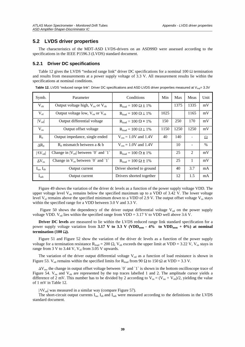
ATLAS Muon Spectrometer - Monitored Drift TubesASD Amplifier-Shaper-Discriminator IC
Appendix - LVDS driver properties
39
5.2 LVDS driver propertiesThe characteristics of the MDT-ASD LVDS-drivers on an ASD99D were assessed according to the
specifications in the IEEE P1596.3 (LVDS) standard document.
5.2.1 Driver DC specifications
Table 12 gives the LVDS “reduced range link” driver DC specifications for a nominal 100 : terminationand results from measurements at a power supply voltage of 3.3 V. All measurement results lie within thespecifications at nominal conditions.
Table 12. LVDS “reduced range link”: Driver DC specifications and ASD LVDS driver properties measured at Vsup= 3.3V
Symb. Parameter Conditions Min Max Meas Unit
Voh Output voltage high, Voa or Vob Rload = 100 : r 1% 1375 1335 mV
Vol Output voltage low, Voa or Vob Rload = 100 : r 1% 1025 1165 mV
|Vod| Output differential voltage Rload = 100 : r 1% 150 250 170 mV
Vos Output offset voltage Rload = 100 : r 1% 1150 1250 1250 mV
R0 Output impedance, single ended Vcm = 1.0V and 1.4V 40 140 - :
'R0 R0 mismatch between a & b Vcm = 1.0V and 1.4V 10 - %
|'Vod| Change in |Vod| between `0` and `1` Rload = 100 : r 1% 25 2 mV
'Vos Change in Vos between `0` and `1` Rload = 100 : r 1% 25 1 mV
Isa, Isb Output current Driver shorted to ground 40 3.7 mA
Isab Output current Drivers shorted together 12 1.5 mA
Figure 49 shows the variation of the driver dc levels as a function of the power supply voltage VDD. Theupper voltage level Voh remains below the specified maximum up to a VDD of 3.42 V. The lower voltagelevel Vol remains above the specified minimum down to a VDD of 2.9 V. The output offset voltage Vos stayswithin the specified range for a VDD between 3.0 V and 3.3 V.
Figure 50 shows the dependency of the driver output differential voltage Vod on the power supplyvoltage VDD. Vod lies within the specified range from VDD = 3.17 V to VDD well above 3.6 V.
Driver DC levels are measured to lie within the LVDS reduced range link standard specification for apower supply voltage variation from 3.17 V to 3.3 V (VDDnom - 4% to VDDnom + 0%) at nominaltermination (100 ::).
Figure 51 and Figure 52 show the variation of the driver dc levels as a function of the power supplyvoltage for a termination resistance Rload = 200 :, Voh exceeds the upper limit at VDD = 3.22 V, Vos stays inrange from 3 V to 3.44 V, Vol from 3.05 V upwards.
The variation of the driver output differential voltage Vod as a function of load resistance is shown inFigure 53. Vod remains within the specified limits for Rload from 90 : to 150 : at VDD = 3.3 V.
'Vos, the change in output offset voltage between `0` and `1` is shown in the bottom oscilloscope trace ofFigure 54. Voa and Vob are represented by the top traces labelled 1 and 2. The amplitude cursor yields adifference of 2 mV. This number has to be divided by 2 according to Vos = (Voa + Vob)/2, yielding the valueof 1 mV in Table 12.
|'Vod| was measured in a similar way (compare Figure 57).The short-circuit output currents Isa, Isb and Isab were measured according to the definitions in the LVDS
standard document.
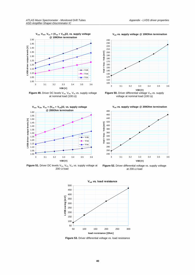
ATLAS Muon Spectrometer - Monitored Drift TubesASD Amplifier-Shaper-Discriminator IC
Appendix - LVDS driver properties
40
Voa, Vob, Vos = (Voa + Vob)/2, vs. supply voltage @ 100Ohm termination
1.00
1.05
1.10
1.15
1.20
1.25
1.30
1.35
1.40
1.45
1.50
3 3.1 3.2 3.3 3.4 3.5 3.6
VDD [V]
LV
DS
dri
ver
ou
tpu
t le
vels
[V
]
Vob
Voa
Vos
Figure 49. Driver DC levels Voa, Vob, Vos vs. supply voltageat nominal load (100 :)
Vod vs. supply voltage @ 100Ohm termination
100
110
120
130
140
150
160
170
180
190
200
210
220
230
240
3 3.1 3.2 3.3 3.4 3.5 3.6
VDD [V]
Vo
d =
Vo
a -
Vo
b [
mV
]
Figure 50. Driver differential voltage Vod vs. supplyvoltage at nominal load (100 :)
Voa, Vob, Vos = (Voa + Vob)/2, vs. supply voltage @ 200Ohm termination
1.00
1.05
1.10
1.15
1.20
1.25
1.30
1.35
1.40
1.45
1.50
1.55
1.60
3 3.1 3.2 3.3 3.4 3.5 3.6
VDD [V]
LV
DS
dri
ver
ou
tpu
t le
vels
[V
]
Vob
Voa
Vos
Figure 51. Driver DC levels Voa, Vob, Vos vs. supply voltage at200 : load
Vod vs. supply voltage @ 200Ohm termination
240
260
280
300
320
340
360
380
400
420
440
460
480
3 3.1 3.2 3.3 3.4 3.5 3.6
VDD [V]
Vo
d =
Vo
a -
Vo
b [
mV
]
Figure 52. Driver differential voltage vs. supply voltageat 200 : load
Vod vs. load resistance
50
100
150
200
250
300
350
400
450
500
50 100 150 200 250 300
load resistance [Ohm]
LV
DS
sw
ing
[m
V]
Figure 53. Driver differential voltage vs. load resistance
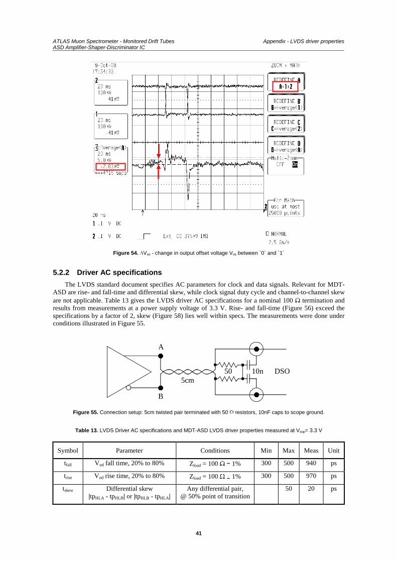
ATLAS Muon Spectrometer - Monitored Drift TubesASD Amplifier-Shaper-Discriminator IC
Appendix - LVDS driver properties
41
Figure 54. 'Vos - change in output offset voltage Vos between `0` and `1`
5.2.2 Driver AC specifications
The LVDS standard document specifies AC parameters for clock and data signals. Relevant for MDT-ASD are rise- and fall-time and differential skew, while clock signal duty cycle and channel-to-channel skeware not applicable. Table 13 gives the LVDS driver AC specifications for a nominal 100 : termination andresults from measurements at a power supply voltage of 3.3 V. Rise- and fall-time (Figure 56) exceed thespecifications by a factor of 2, skew (Figure 58) lies well within specs. The measurements were done underconditions illustrated in Figure 55.
A
B
505cm
10n DSO
Figure 55. Connection setup: 5cm twisted pair terminated with 50 : resistors, 10nF caps to scope ground.
Table 13. LVDS Driver AC specifications and MDT-ASD LVDS driver properties measured at Vsup= 3.3 V
Symbol Parameter Conditions Min Max Meas Unit
tfall Vod fall time, 20% to 80% Zload = 100 : r 1% 300 500 940 ps
trise Vod rise time, 20% to 80% Zload = 100 : r 1% 300 500 970 ps
tskew Differential skew|tpHLA - tpHLB| or |tpHLB - tpHLA|
Any differential pair,@ 50% point of transition
50 20 ps
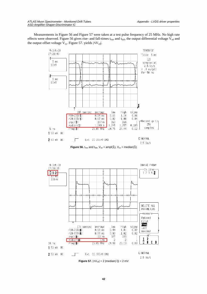
ATLAS Muon Spectrometer - Monitored Drift TubesASD Amplifier-Shaper-Discriminator IC
Appendix - LVDS driver properties
42
Measurements in Figure 56 and Figure 57 were taken at a test pulse frequency of 25 MHz. No high rateeffects were observed. Figure 56 gives rise- and fall-times trise and tfall, the output differential voltage Vod andthe output offset voltage Vos. Figure 57. yields |'Vod|.
Figure 56. trise and tfall, Vod = ampl(1), Vos = median(1)
Figure 57. |'Vod| = 2 |median($)| = 2 mV
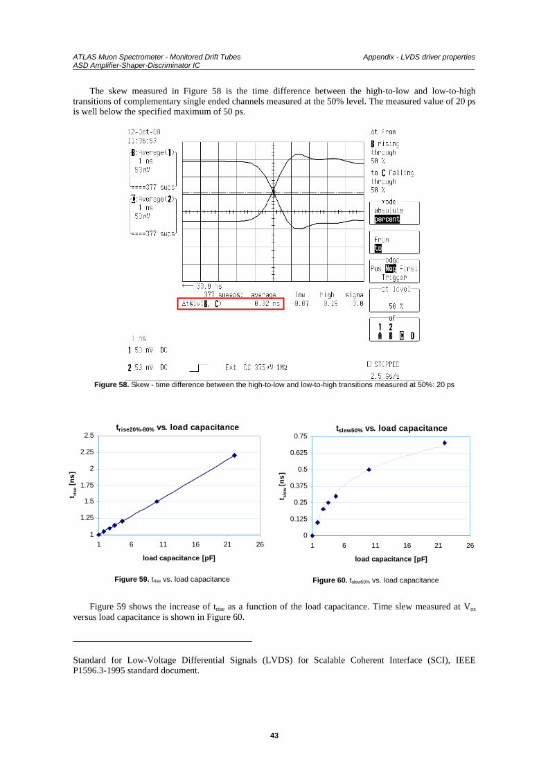
ATLAS Muon Spectrometer - Monitored Drift TubesASD Amplifier-Shaper-Discriminator IC
Appendix - LVDS driver properties
43
The skew measured in Figure 58 is the time difference between the high-to-low and low-to-hightransitions of complementary single ended channels measured at the 50% level. The measured value of 20 psis well below the specified maximum of 50 ps.
Figure 58. Skew - time difference between the high-to-low and low-to-high transitions measured at 50%: 20 ps
trise20%-80% vs. load capacitance
1
1.25
1.5
1.75
2
2.25
2.5
1 6 11 16 21 26
load capacitance [pF]
t ris
e [
ns
]
Figure 59. trise vs. load capacitance
tslew50% vs. load capacitance
0
0.125
0.25
0.375
0.5
0.625
0.75
1 6 11 16 21 26
load capacitance [pF]
t slew
[n
s]
Figure 60. tslew50% vs. load capacitance
Figure 59 shows the increase of trise as a function of the load capacitance. Time slew measured at Vos
versus load capacitance is shown in Figure 60.
Standard for Low-Voltage Differential Signals (LVDS) for Scalable Coherent Interface (SCI), IEEEP1596.3-1995 standard document.
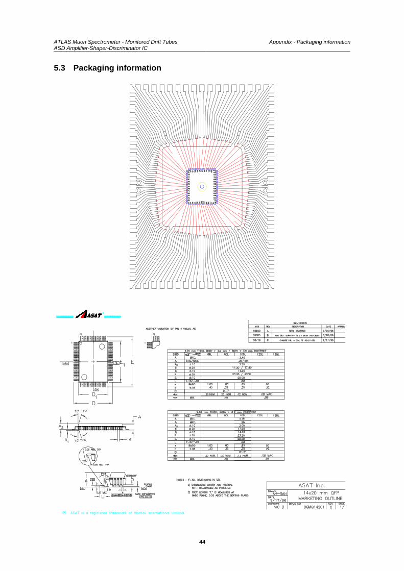
ATLAS Muon Spectrometer - Monitored Drift TubesASD Amplifier-Shaper-Discriminator IC
Appendix - Packaging information
44
5.3 Packaging information
ATLAS Muon Spectrometer - Monitored Drift TubesASD Amplifier-Shaper-Discriminator IC
References
6 References
[1] M. Aleksa, W. Riegler, Non-Linear MDT Drift Gases like Ar/CO2, ATLAS Internal Note, ATL-MUON-98-268, Dec. 1998
[2] M. Aleksa, M. Deile, N. Hessey, W. Riegler, MDT Performance in a High Rate BackgroundEnvironment, ATLAS Internal Note, ATL-MUON-98-258, Oct. 1998
[3] Y. Arai, AMT-1, ATLAS Muon TDC Version 1, User’s Manual, KEK, http://atlas.kek.jp/~araiy,June 2000
[4] Y. Arai, Preliminary Design Review of the MDT Electronics (TDC part)http://arkhp01.kek.jp:80/~araiy/TDC_PDR.pdf, Feb. 2001
[5] C. Blocker, John Huth, John Oliver, Noise Considerations for the Atlas Muon Front-End Electronics,ATLAS Internal Note, MUON-NO-080, CERN, April 1995
[6] F.Faccio, C.Detcheverry, M.Huhtinen, First evaluation of the Single Event Upset (SEU) risk forelectronics in the CMS experiment, CMS Internal Note, CERN CMS NOTE 1998/054 (1998)
[7] P. Jarron, G. Anelli, T. Calin, J. Cosculluela, M. Campbell, M. Delmastro, F. Faccio, A. Giraldo, E.Heijne, K. Kloukinas, M. Letheren, M. Nicolaidis, P. Moreira, A. Paccagnella, A. Marchioro,W. Snoeys, R. Velazco, Deep submicron CMOS technologies for the LHC experiments, NuclearPhysics B (Proc. Suppl.) 78 (1999) 625 - 634
[8] K.J. Hass, J.W. Gambles, B. Walker, M. Zampaglione, Mitigating Single Event Upsets FromCombinational Logic, in Proceedings of 7th NASA Symp. on VLSI design, 1998
[9] E. Hazen , J. Shank, T. Giordano, J. Huth, J. Oliver, Status of the Front End Electronics for the MDTSystem, ATLAS Internal Note, MUON-NO-111, CERN, March 1996
[10] J. Huth , A. Liu, J. Oliver, Note on Noise Contribution of the Termination Resistor in the MDTs,ATLAS Internal Note, ATL-MUON-96-127, CERN, Aug. 1996
[11] J. Huth, J. Oliver, W. Riegler, E. Hazen, C. Posch, J. Shank, Development of an Octal CMOS ASDfor the ATLAS Muon Detector, Proceedings of the Fifth Workshop on Electronics for LHCExperiments, CERN/LHCC/99-33, Oct. 1999
[12] F. M. Newcomer, S. Tedja, R. Van Barg, J. Van der Spiegel, H. H. Williams, IEEE Transactions onNuclear Science NS-40 (4), March 1993
[13] G. Novak, C. Posch, W. Riegler, Particle identification in the ATLAS Muon Spectrometer, ATLASInternal Note, to be released, CERN, June 2001
[14] J.V. Osborn, D.C. Mayer, R.C. Lacoe, S.C. Moss, and S.D. La Lumondiere, Single event latchupcharacteristics of three commercial CMOS processes, in Proceedings of 7th NASA Symp. on VLSIdesign, 1998
[15] J.V. Osborn, R.C. Lacoe, D.C. Mayer, and G. Yabiku, Total Dose Hardness of Three CommercialCMOS Microelectronics Foundries, IEEE Trans. Nucl. Sci., vol. 45, p. 1458, 1998.
[16] W. Riegler, MDT Resolution Simulation - Front-end Electronics Requirements, ATLAS InternalNote, MUON-NO-137, CERN, Jan. 1997
[17] W. Riegler, MDT Efficiency – Double Track Separation, ATLAS Internal Note, MUON-NO-173,CERN, Oct. 1997
ATLAS Muon Spectrometer - Monitored Drift TubesASD Amplifier-Shaper-Discriminator IC
References
46
[18] W. Riegler, Limits to Drift Chamber Resolution, PhD Thesis, Vienna University of Technology,Vienna, Austria, Nov. 1997
[19] W. Riegler, M. Aleksa, Bipolar versus unipolar shaping of MDT signals, ATLAS Internal Note,ATL-MUON-99-003, Mar. 1999
[20] R. Veenhof, GARFIELD – simulation of gaseous detectors, http://consult.cern.ch/writeup/garfield/,CERN web page, 1984 – 2000
[21] N.K. Verghese, T.J. Schmerbeck, D.J. Allstot, Simulation techniques and solutions for mixed-signalcoupling in integrated circuits, Kluwer Acedemic Publishers.
[22] ATLAS Front End Electronics Co-ordination, Preliminary List of Criteria for IC Design Reviews,http://atlas.web.cern.ch/Atlas/GROUPS/FRONTEND/WWW/ic_desig.pdf, CERN, Nov. 1998
[23] Standard for Low-Voltage Differential Signals (LVDS) for Scalable Coherent Interface (SCI), IEEEP1596.3-1995, IEEE Standard Document, 1995
[24] MOSIS web site, http://www.mosis.org/Technical/menu-technical.html
[25] MOSIS web site, Hewlett Packard (HP) AMOS14TB Process - 0.50 micron feature size,http://www.mosis.org/Technical/Processes/proc-hp-amos14tb.html
[26] Tanner Hi-ESD Pad Library for the HP AMOS14B 0.5P process, http://www.mosis.org/cell-libraries/scn05-pads-tiny/mHP05P.pdf, Tanner Research Inc., 1999