Embed Size (px)
Citation preview


Airborne AvengerOperation, Maintenance and Service Manual
ATARI INC1265 BORREGAS AVENUEP.O. BOX 9027SUNNYVALE, CA 94086408/745-2000 • TELEX 35-7488

All rights reserved. Copyright © 1977 by Atari, Inc. No part of this publication may be reproduced by any mechanical, photographic, orelectronic process, or in the form of a phonographic recording, nor may it be stored In a retrieval system, transmitted, or otherwise copied forpublic or private use, without permission from the publisher.
For permission requests, write:
ATARI INC1265 BORREGAS AVENUEP.O. BOX 9027SUNNYVALE, CALIFORNIA 94086
Location of Serial NumbersYour game's serial number is stamped on all four printed circuit boards, in the locations shown below. The same number is also stamped onthe label located on the rear of the back box. Please mention this number whenever calling your distributor for service.
Location of Serial Numbers
WARRANTYSeller warrants that its printed circuit boards and parts thereon are free from defects in material and workmanship under normal use andservice for a period of ninety (90) days from date of shipment. Seller warrants that its television monitors (in games supplied with monitors)are free from defects in material and workmanship under normal use and service for a period of thirty (30) days from date of shipment. Noneof the Seller's other products or parts thereof are warranted.
It the products described in this manual fail to conform to this warranty, Sellers' sole liability shall be, at its option, to repair, replace, or creditBuyer's account for such products which are returned to Seller during said warranty period, provided:
Seller is promptly notified in writing upon discovery by Buyer that said products are defective;a.
Such products are returned prepaid to Seller's plant; andb.
Seller's examination of said products discloses to Seller's satisfaction that such alleged defects existed and were not caused by accident,misuse, neglect, alteration, improper repair, installation or improper testing.
c.
In no event shall Seller be liable for loss of profits, loss of use, incidental or consequential damages.
EXCEPT FOR ANY EXPRESS WARRANTY SET FORTH IN A WRITTEN CONTRACT BETWEEN SELLER AND BUYER WHICHCONTRACT SUPERSEDES THE TERMS OF THIS ORDER, THIS WARRANTY IS EXPRESSED IN LIEU OF ALL OTHERWARRANTIES EXPRESSED OR IMPLIED, INCLUDING THE IMPLIED WARRANTIES OF MERCHANTABILITY AND FITNESSFOR A PARTICULAR PURPOSE, AND OF ALL OTHER OBLIGATIONS OR LIABILITIES ON THE SELLLER'S PART, AND ITNEITHER ASSUMES NOR AUTHORIZES ANY OTHER PERSON TO ASSUME FOR THE SELLER ANY OTHER LIABILITIES INCONNECTION WITH THE SALE OF PRODUCTS UNDER THIS ORDER.
This document is and contains confidential trade secret information of Atari, Inc.
This document is loaned under confidential custody for the sole purpose of operation, maintenance or repair of Atari equipment and may notbe used by or disclosed to any person for any other purpose whatever, and remains the property of Atari, Inc.
Neither it nor the information it contains may be reproduced, used, or disclosed to persons not having a need to know consistent with thepurpose of the loan, without written consent of Atari, Inc.
Forward to the Table of Contents

Back to the top of the manualForward to Chapter 1
Table of ContentsTop of Manual●
Location of Serial Numbers●
Warranty●
Table of Contents●
Table of Figures●
Table of Tables●
Chapter 1: Location Setup
Inventory of Parts in Shipping CartonsA.
Assembly of Game
Assembly of Legs and Back Box1.
Attach Back Box2.
Final Inspection3.
Final Assembly4.
B.
Decription of Game OptionsC.
Setting the OptionsD.
Self-TestE.
Volume AdjustmentF.
I.
Chapter 2: Game Play
Attract ModeA.
Play Mode
Game Play and Scoring1.
Tilt Condition2.
Match Option3.
B.
II.
Chapter 3: Maintenance and Adjustments
Cleaning
Game Cabinet Exterior1.
Playfield2.
A.
Fuse ReplacementB.
III.

Coin Mechanism
Components on Coin Door1.
Access to Coin Mechanisms2.
Clearing of Coin Path3.
Adjustment of Coin Switch Trip Wire4.
Mechanical Adjustments on Coin Mechanism5.
Lubrication6.
General Troubleshooting Hints7.
C.
Game Controls and Playfield Components
Solenoid Fuses1.
Troubleshooting of Playfield Switches Connected in Parallel2.
D.
Gas-Discharge Displays
Preliminary Operational Checks1.
Check on +90 and -90 Volts Power Supply Voltages2.
Score Panel Removal and Visual Checks3.
Replacement of Score Panel4.
Removing Display Assembly5.
Installing the Display Assembly6.
E.
Lamp Replacement
Playfield Lamps1.
Back Box Lamps2.
F.
Adjustment of Speaker VolumeG.
Chapter 4: Theory of Operation
IntroductionA.
Components of the Microcomputer System
Microprocessing Unit1.
Program Memory2.
Data Memory3.
Memory Output Latches4.
Clock Generator5.
Tri-State Buffers6.
Control Logic7.
B.
Circuit DescriptionsC.
IV.

Solenoid Driver Circuits1.
Lamp Driver Circuits2.
Switch Sensing Circuit3.
Displays and Display Data4.
Credit and Match/Ball Display Circuit5.
Score Display Circuit6.
Sound Generator and Speaker Driver Circuits7.
Table of FiguresFigure 1: Inventory of Accessories●
Figure 2: Attaching Legs without Pin Jack●
Figure 3: Attaching Back Box●
Figure 4: Final Assembly and Inspection●
Figure 5: Location of Option Swtiches●
Figure 6: Location of Playfield Switches and Solenoids●
Figure 7: Playfield Rubber Sizes●
Figure 8: Coin Door Assembly●
Figure 9: Hinging Open the Magnet Gate Assembly●
Figure 10: Removal of Coin Mechanism●
Figure 11: Surfaces to Clean inside the Coin Mechanism●
Figure 12: Removal of Plate Covering Rear of Coin Slot●
Figure 13: Detail View of Coin Switch and Trip Wire●
Figure 14: Coin Mechanism, Exploded View●
Figure 15: Close-up View of Lubrication Point●
Figure 16: Top View of Score and Match/Credit Display Assembly●
Figure 17: Removal of Score Panel●
Figure 18: Score Panel Terminals●
Figure 19: Line-up of Terminal Pins and Terminal Strips●
Figure 20: Lower Right Comer of Display Assembly●
Figure 21: Location of Technician Adjustment for Speaker Volume●
Figure 22: Functional Block Diagram●
Figure 23: Block Diagram of Microcomputer System●

Figure 24: Airborne Avenger Wiring Diagram●
Figure 25-A: Processor PCB Schematic Diagram●
Figure 25-B: Processor PCB Assembly Drawing●
Figure 25-C: Processor PCB Assembly Parts List●
Figure 26-A: Processor PCB Schematic Diagram●
Figure 26-B: Processor PCB Assembly Drawing●
Figure 26-C: Processor PCB Assemmbly Parts List●
Figure 26-D: Processor PCB Parts List●
Figure 27-A: Auxiliary PCB Schematic Diagram●
Figure 27-B: Auxiliary PCB Assembly Diagram●
Figure 27-C: Auxiliary PCB Assembly Parts List●
Figure 28-A: Match/Credit PCB Schematic Diagram●
Figure 28-B: Match/Credit PCB Assembly Drawing●
Figure 28-C: Match/Credit PCB Assembly Parts List●
Figure 29-A: Score Panel Drive PCB Schematic Diagram●
Figure 29-B: Score Panel Drive PCB Assembly Drawing●
Figure 29-C: Figure 28-C: Score Panel Drive PCB Assembly List●
Figure 30: Simplified Diagram of Basic Solenoid Driver Circuit●
Figure 31: Additional Components to be Installed for Each Metering Function Added●
Figure 32: Simplified Diagram of Basic Lamp Driver Circuit●
Figure 33: Simplified Diagram of Switch Sensing Circuit●
Figure 34: Simplified Diagram of Switch Censing Circuit Waveforms●
Figure 35: Waveforms for Gas Discharge Displays●
Figure 36: Arrangement of Connections to Score Panel●
Table of TablesTable 1: Self-Test Procedure●
Table 2: Replay Level Settings●
Table 3: Maximum Credit Settings●
Table 4: Switch Identification●
Table 5: Solenoid Identification●
Table 6: Coin/Credit Mode Switch Settings●

Table 7: Replay/Add-a-Ball Switch Settings●
Table 8: Match Switch Settings●
Table 9: Slam/Tilt Sound Switch Settings●
Table 10: "Special" Mode Switch Settings●
Table 11: AIRBORNE AVENGER Spellout Setting●
Table 12: Last Ball Bonus Setting●
Table 13: Fuses Located Near Ball Shooter●
Table 14: Fuses Located on Power Supply Assembly●
Table 15: Componenets Required for Special Metering Functions●
Back to the top of the manualForward to Chapter 1

Up to the table of contentsForward to Chapter 2
Chapter 1: LOCATION SETUPNOTE: If reading through this manual does not lead to solving your specific problem, you can reach Atari's Customer Service Department bytelephone (open Monday through Friday, 7:30 a.m. to 4:00 p.m. Pacific Time); From inside California, Alaska or Hawaii: (408) 984-1900From the remaining 47 states, toll-free: (800) 538-6892
A. INVENTORY OF PARTS IN SHIPPING CARTONSAs you already know, Atari's Airborne Avenger(TM) came to you packaged in one big carton containing 1) game cabinet 2) back box carton,and 3) accessories carton. Contained in the accessories box were the game cabinet legs, cash box, and this manual. Keys to the coin door aretaped to the top back of the game cabinet. Keys to the back box are taped to the bottom of the back box.
Open the cash box and take an inventory of accessories as shown in Figure 1.
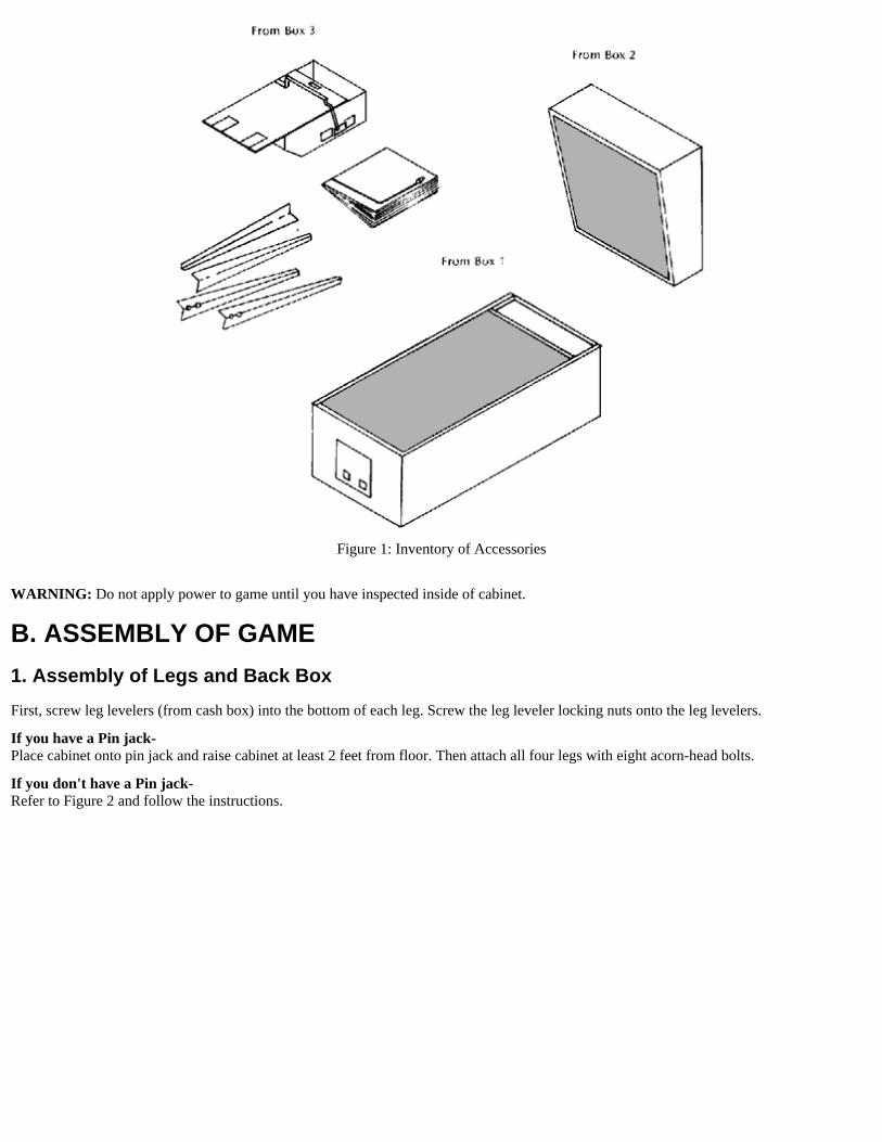
Figure 1: Inventory of Accessories
WARNING: Do not apply power to game until you have inspected inside of cabinet.
B. ASSEMBLY OF GAME
1. Assembly of Legs and Back Box
First, screw leg levelers (from cash box) into the bottom of each leg. Screw the leg leveler locking nuts onto the leg levelers.
If you have a Pin jack-Place cabinet onto pin jack and raise cabinet at least 2 feet from floor. Then attach all four legs with eight acorn-head bolts.
If you don't have a Pin jack-Refer to Figure 2 and follow the instructions.

Figure 2: Attaching Legs without a Pin Jack

2. Attach Back Box
CAUTION: Back Box carton is labeled "THIS SIDE UP^" Set the Back Box carton as labeled before removing the Back Box from thecarton. This will prevent the Back Box glass from failing out and breaking.
Remove the Back Box and Back Box Key Envelope from the Back Box carton and attach the Back Box to the pin cabinet as instructed inFigure 3.
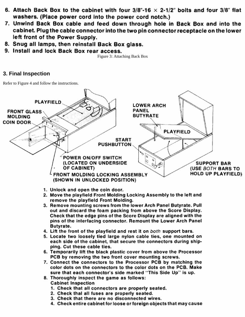
Figure 3: Attaching Back Box
3. Final Inspection
Refer to Figure 4 and follow the instructions.

Figure 4: Final Assembly and Inspection
4. Final Assembly
NOTE: The tilt bob is made of a soft material, carbon: don't overtighten.
Install the tilt bob (from cash box) onto the pendulum wire at the right front side of the pin cabinet. Tighten the thumbscrew lightly andleave it pointing toward the coin door. This way it will be accessible from the coin door for fine tuning after the playfield is lowered.
1.
Place one ball onto the playfield and the other ball (both from cash box) into the captive ball area (located in the center of the playfield).2.
Choose the proper instruction cards (from cash box) and attach to the lower arch panel butyrate as illustrated in Figure 5.3.
Install the cash box.4.
Lower the playfield and install the playfield glass (for help, refer to Figure 4).5.
Level the playfield for a 3¡ slope from the rear to the front of the playfield.6.
Insert the power plug into a 115 VAC power source.7.
C. DESCRIPTION OF GAME OPTIONSSeveral options are available for structuring Airborne Avenger(TM) for maximum returns at your location. The following is a list of theseoptions:
Sixteen coin/credit settings for each coin chute1.
Four maximum credit levels2.
Automatic double bonus for last ball or not3.
Match or no match4.
Four different choices for "special" (20,000 points, 30,000 points, free game or extra ball)5.
Three- or five-ball game6.
Add-a-ball or not7.
Replay or no replay8.
Extra ball or 20,000 points for spellout of AIRBORNE AVENGER9.
D. SETTING THE OPTIONSWARNING: Power should never be on while setting the options. Dangerous voltages are present inside the game cabinet.
All the options are selectable by merely flipping a switch. Refer to Self-Test Procedure in Table 1. Tables 2, 3, and 6 through 10 list all theoptions and the switches necessary to set those options. In these tables, all manufacturer suggested settings are marked with asterisks. Figure 5shows the location of each switch on the Processor PCB (printed circuit board). To set the switches, lightly press down on the selected switchtoggles with a small pointed object. To set the toggle to on, press on the switch side toward the closest end of the Processor PCB.

Figure 5: Location of Option Switches
E. SELF-TESTSelf-Test is activated by pressing the TEST pushbutton. The TEST pushbutton is located at the inside top middle of the coin door. Pressing thepushbutton once, begins the lamp test pressing the pushbutton twice, begins the switch test; and the third time, the solenoid test. Pressing thepushbutton the fourth time causes the game to exit the Self-Test mode and enter the attract mode of operation,
Please read the following Suggestions, then perform the Self-Test Procedure described in Table 1.
As an aid for locating the playfield switches and solenoids, see Figure 6.
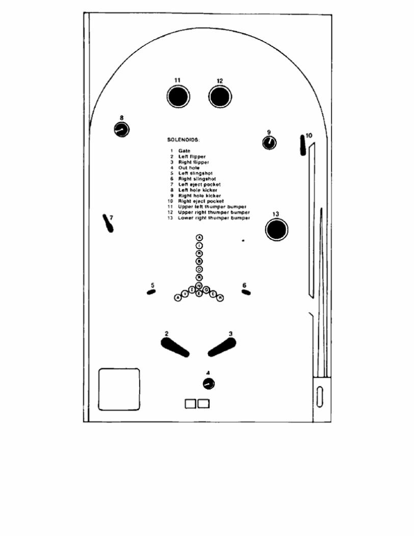

Figure 6: Location of Playfield Switches and Solenoids
NOTE: Toggle 1 of PROG SW1 on Processor PCB should always remain in off position. For bench test purposes, Self-Test mode may beactivated by setting PROG SW1 toggle 1 to on then off. This simulates pressing the TEST pushbutton.

SUGGESTION: Perform Self-Test no less than each time the cash box is collected. Machines in good operating condition have been provento earn more money.
SUGGESTION: While performing Self-Test, inspect the playfield for worn rubbers or dirt. Clean the playfield glass and outside of thecabinet regularly. Clean games attract more players and therefore earn more money
F. VOLUME ADJUSTMENTThe volume control for all game sounds is located inside the cabinet above and to the right of the game speaker To adjust the volume, turn thevolume control clockwise to increase the volume and counter-clockwise to decrease the volume.
A second volume control is located inside the cabinet on the Auxiliary PCB (labeled VOL). This volume control should only be adjusted by aqualified technician. Technicians may learn the proper adjustment of this control by reading the instructions in the Maintenance chapter(Chapter 3) of this manual.
Table 1: Self-Test ProcedureTest Name Test Instruction Indication of of Test Mode Test Results Operator Action
Lamp Test Press and release (once only)the TEST pushbutton. (TheTEST pushbutton is located onthe inside top middle of thecoin door.)
(Test number) 1 appears in4TH UP player scoredisplay.
All lamps are lighted (ignoreback boxlamps).
Check to ensure that alllamps are lighted.
High replay level is displayed in1ST UP player score display.
Medium replay level isdisplayed in 2ND UP scoredisplay.
Low replay level is displayed in3RD UP player score display.
To change, adjust ReplayRotary switch and PROGSW1 toggle 4 for the resultsas listed in Table 2.
Number of balls per game isdisplayed in BALL display.
To change, set DIP switchPROG SW 2 toggle 1 to ONfor 3 balls, OFF for 5 balls.
Maximum credits is displayedin CREDIT display.
To change, set DIP switchPROG SW 1 toggles 5 and 6as listed in Table 3.NOTE: To exit Self-Test,press and release the TESTpushbutton three times.
Switch Test Press and release (once only)TEST pushbutton.
(Test number) 2 appears in4TH UP player scoredisplay.
Any activated or stuck switchesare identified by a number inthe CREDIT display. A pulsingtone is heard when a switch isactivated or stuck.
Identify activated or stuckswitches as listed in Table 4.NOTE: To exit Self-Test,press and release the TESTpushbutton two times.
Solenoid Test Press and release (once only)TEST pushbutton.
(Test number) 3 appears in4TH UP player scoredisplay.
Each solenoid is individuallyenergized and identified by anumber in the CREDIT display.
Press left flipper button toactivate solenoid. Press rightflipper button to change tonext solenoid. Identify eachsolenoid with number inCREDIT display as listed inTable 5.NOTE: To exit Self-Test,press and release the TESTpushbutton one time.
Table 2 Replay Level SettingsRotarySwitchSetting
PROG SW1Toggle 4
Low ReplayLevel
Medium ReplayLevel
High ReplayLevel
0 OFF 50,000 70,000 90,000

1 OFF 60,000 90,000 120,0002 OFF 70,000 100,000 130,0003 OFF 80,000 120,000 160,0004 OFF 90,000 130,000 170,000
*5 OFF 100,000 150,000 200 0006 OFF 110,000 160,000 210,0007 OFF 120,000 180,000 240,0008 OFF 130,000 190,000 250,0009 OFF 140,000 210,000 280,000
10 OFF 150,000 220,000 290,00011 OFF 160,000 240,000 320,00012 OFF 170,000 250,000 330,00013 OFF 180,000 270,000 360,00014 OFF 190,000 280,000 370,00015 OFF 200,000 300,000 400,0000 ON 210,000 310,000 410,0001 ON 220,000 330,000 440,0002 ON 230,000 340,000 450,0003 ON 240,000 360,000 480,0004 ON 250,000 370,000 490,0005 ON 260,000 390,000 520,0006 ON 270,000 400,000 530,0007 ON 280,000 420,000 560,0008 ON 290,000 430,000 570,0009 ON 300,000 450,000 600,000
10 ON 310,000 460,000 610,00011 ON 320,000 480,000 640,00012 ON 330,000 490,000 650,00013 ON 340,000 510,000 680,00014 ON 350,000 520,000 690,00015 ON 360,000 540,000 720,000
*Indicates manufacturers suggested setting
Table 3: Maximum Credit SettingsMaximum Credits Prog Sw1 Toggle 5 Prog Sw1 Toggle 6
*8 OFF OFF12 ON OFF15 OFF ON20 ON ON
*Indicates manufacturers suggested setting
Table 4: Switch identificationCredit Number Location
1 Left coin switch2 Right coin switch3 START pushbutton4 Coin door slam switch
17 Cabinet slam switch18 Tilt pendulum19 Left flipper

20 Right flipper21 Center target (#4)22 Upper right target (#3)23 Upper left target (#2)24 Lower left target (#1)34 Lower ball lane (inside left)35 Lower ball lane (middle left)36 Lower ball lane (outside left)37 Top center ball lane (right)38 Top center ball lane (left)
39Lower ball lanes(outside and inside right)
40 Lower ball lane (middle right)41 Left hole kicker42 Lower right thumper bumper43 Upper right thumper bumper44 Upper left thumper bumper45 Spinning target46 Right eject pocket47 Left eject pocket48 Right hole kicker49 Left slingshot50 10 points (5 switches)51 50 points (8 switches)52 Outhole56 Right slingshot57 50 and letter advance58 Captive ball rollover59 Center rollover (B)60 Upper right roll-thru
Table 5: Solenoid IdentificationCredit Display Number Solenoid
1 Gate2 Left flipper3 Right flipper4 Outhole5 Left slingshot6 Right slingshot7 Left elect pocket8 Left hole kicker9 Right hole kicker
10 Right eject pocket11 Upper left thumper bumper12 Upper right thumper bumper13 Lower right thumper bumper
Table 6: Coin/Credit Mode Switch SettingsCoin/Credit For: PROG SW2 Toggles
Left Coin Chute Right Coin Chute 3 4 5 6

*1 coin, 1 credit *1 coin, 1 credit OFF OFF OFF OFF1 coin, 2 credits 1 coin, 2 credits ON OFF OFF OFF1 coin, 3 credits 1 coin, 3 credits OFF ON OFF OFF1 coin, 4 credits 1 coin, 4 credits ON ON OFF OFF2 coins, 1 credit 2 coins, 1 credit OFF OFF ON OFF
**2 coins, 3 credits **2 coins, 3 credits ON OFF ON OFF**2 coins, 5 credits **2 coins, 5 credits OFF ON ON OFF
2 coins, 1 credit 1 coin, 1 credit ON ON ON OFF1 coin, 1 credit 1 coin, 2 credits OFF OFF OFF ON
1 coin, 2 credits 1 coin, 4 credits ON OFF OFF ON1 coin, 3 credits 1 coin, 6 credits OFF ON OFF ON
**2 coins, 3 credits **2 coins, 7 credits ON ON OFF ON**2 coins, 5 credits 1 coin, 5 credits OFF OFF ON ON**2 coins, 7 credits 1 coin, 7 credits ON OFF ON ON***3 coins, 1 credit 1 coin, 1 credit OFF ON ON ON
1 coin, 1 credit 1 coin, 3 credits ON ON ON ON*Indicates manufacturers suggested setting**Indicates second coin gives 1 more credit than first coin,provided no scoring is achieved between coins.***Indicates no credit until third coin is accepted
Table 7: Replay/Add-A-Ball Switch SettingsReplay/Add-A-Ball for
Exceeding Replay ScorePROG SW1
Toggle 7PROG SW1
Toggle 8No replay, no add-a-ball OFF OFFAdd-a-ball ON OFF*Replay OFF ONReplay ON ON*Indicates manufacturers suggested setting
Table 8: Match Switch Setting
Match PROG SW2Toggle 2
Match off OFF*Match on ON*Indicates manufacturers suggested setting
Table 9: Ball Setting
Balls Per Game PROG SW2Toggle 1
3 Balls ON5 Balls OFF
Table 10: "Special" Mode Switch Settings
"Special Mode" PROG SW2Toggle 7
PROG SW2Toggle 8
Extra ball for Special OFF OFF*Replay for Special ON OFF

20,000 points for Special OFF ON20,000 points for Special ON ON*Indicates manufacturers suggested setting
Table 11: AIRBORNE AVENGER Spellout Setting
Spellout Reward PROG SW1Toggle 2
Extra Ball Awarded for Spellout OFF20,000 Points Awarded for Spellout ON
Table 12: Last Ball Bonus Setting
Last Ball Reward PROG SW1Toggle 3
No Double Bonus for Last Ball OFFDouble Bonus for Last Ball ON
Up to the table of contentsForward to Chapter 2
Up to the table of contentsBack to Chapter 1Forward to Chapter 3

Chapter 2: GAME PLAYThe game has three modes of operation: attract, play, and Self-Test. The attract mode serves to attractplayers to the game. The play mode is active when the game is being played. Self-Test is used by theoperator for game maintenance.
A. ATTRACT MODEThe attract mode is initiated by game power-up, exit from SeIf-Test, or by the end of the previous game.If entered from power-up or Self-Test, the score and match/credit displays will indicate all eights. If theattract mode follows a game, the score will indicate the final score of that game. In any case if the gameis untouched, within approximately two minutes the score display will go blank to conserve energy.
In the attract mode, the playfield lamps blink on and off in an exotic light show that attracts potentialplayers to the game. The game remains in this mode unless a player presses the START pushbutton (ifthere are sufficient accumulated credits) or by the operator entering the Self-Test mode by pressing theTEST pushbutton.
B. PLAY MODEAfter a player has depressed the START button, the game responds as follows:
The uppermost row in the Score Panel will indicate two zeros, and the words 1ST UP to the rightof the zeros will start to blink on and off.
1.
The number in the Credit Display decreases by 1.2.
The Match Display will now become the Ball Display and will indicate 01, meaning that the firstgame ball is in play.
3.
The ball is ejected from the outhole and rolls over to the ball shooter.4.
The playfield lamps will stop blinking, and 1000 and BALL IN PLAY lamps will be constantlylighted. All other score-related lamps remain unlighted.
5.
The flipper controls are enabled.6.
On the player panel just above and beside the ball shooter, the lamp behind the numeral 1(surrounded by yellow) will Iight, indicating that so far one player is playing.
7.
Up to this point and even up until the ball hits the first score point object, additional players may beadded to the game. They do this by depositing money (if necessary), and by then depressing the STARTpushbutton. Each time the game responds by adding another row of two zeros in the Score Panel,decreasing the Credit Display by 1, and lighting another lamp just above the ball shooter.
If a ball rolls all the way down to the outhole without achieving any score whatsoever, the outhole kickerwill than eject the bail so that the player can shoot again. But if a ball achieves any score it is counted asone of the play balls.
As soon as the first score points are earned, the Iock-out coil on the coin door is de-energized and the

coin mechanisms will not accept any coins until after the play sequence ends. The game's speaker alsoproduces sounds when score points are earned, as follows:
For 3000 points, a high-pitch, medium-duration tone, immediately followed by a high-pitch,medium-duration tone.
1.
For 2000 points, a low-pitch, short-duration tone.2.
For 1000 points, a low-pitch, short-duration tone.3.
For 500 points, a high-pitch, long-duration tone.4.
For 100 points, a high-pitch, medium-duration tone.5.
For 50 points, a high-pitch, medium-duration tone.6.
For 10 points, a high-pitch, short-duration tone.7.
Game Play and Scoring
Bonus: Bonus advancement is achieved by hitting the various bonus advance targets, rolling theball through one of the two triple bonus advance lanes (when lit), or rolling the ball over one of the3 single bonus advance lanes (when lit) or by placing the ball into the left eject pocket where theplayer receives 2000 pts. and 2 bonus advances for each of "A", "B", and/or " C" lit The bonus hasa maximum advancement of 29,000 points, and is collected at the end of each ball. When doublebonus is achieved, the player collects twice the bonus value he has achieved.
1.
Double Bonus: Double bonus is achieved by lighting A, B, and C in the double bonusaccumulator. "A" is lit by shooting the ball into the left hole kicker or the "Lites A" ball lane, "B"is lit by rolling the ball over the "lites B" rollover or the "lites B" ball lane. "C" is lit by shootingthe ball into the right hole kicker, or by rolling the ball through the "Lites C" ball lanes.
2.
Gate: The ball gate is opened by hitting either stand-up target #3 (upper right) or stand-up target #1(lower Ieft). The gate remains open until the ball goes through the gate or the bail drops into theouthole.
3.
Top Center Ball Lanes: The left and right top center ball lanes are alternately lit, and are changedby hitting any 50 point switch. Each lane will yield 500 points when not lit, or 3000 points and 3bonus advances when lit. Rolling through the left lane will light all 3 lower left lanes, and rollingthrough the right lane will light all 3 lower right lanes, Rolling through either top center ball lanewill light the captive ball rollover and the "lites B" rollover.
4.
Spinner: The spinner target yields 100 pts per rotation or 1000 points per rotation when lit. Thespinner is lit by hitting either the captive-ball target (#4) or the upper left target (#2). The spinnerlight goes out when the ball lands in the left eject pocket.
5.
A, B, C Bonus: When the ball lands in the left eject pocket, the player collects 500 points plus2000 points and 2 bonus advances for each of "A", "B", and "C" he has lit in the left eject pocket.Upon collection, each light is turned out, and the player must relight the letters by achieving theappropriate rollovers or hole kickers in order to collect them again.
6.
Special: The Alternating special is lit when the player lights targets 1 through 4 on a single ball.The special alternates between the lower left drain, lower right drain, and the upper right rollthrough. Both sling shots and the fifty point switches rotate the special. To achieve the special, theball must roll over the rollover where the special light is lit.
7.

Spell-Out: Completing the Spell-out of AIRBORNE AVENGER can result in either an award ofan extra ball or 20,000 points (see switch options in Table 11). The spell-out is advanced by letteradvance hole kickers, ball lanes, and the triple letter advance roll-thru.
8.
Tilt Condition
The game is provided with a pendulum tilt switch, a slam tilt switch on the coin door, and anotherslam-type switch on the floor of the cabinet. if the microcomputer senses any closure of the aboveswitches, it will put the game into a "tilt" condition and light the TILT lamp. A sound is produced whenthe game is tilted.
Match Option
If this is option is selected, after the last player's last ball has reached the outhole the Ball Displaychanges into a Match Display (the lamp behind the word BALL will be unlighted and the lamp behindthe word MATCH will light). A random number is selected by the microcomputer. That number isdisplayed in the MATCH display.
The microcomputer then compares the match number with the two least significant digits in each player'sscore. One game credit will be awarded for each match-up. Therefore a maximum of four matches arepossible after a four-player game has ended.
Up to the table of contentsBack to Chapter 1Forward to Chapter 3

Up to the table of contentsBack to Chapter 2Forward to Chapter 4
CHAPTER 3: MAINTENANCE AND ADJUSTMENTSDue to its solid-state electronic circuitry, this Atari game shouId require very little maintenance and only occasional adjustment. Informationgiven in this chapter and elsewhere in the manual is intended to cover most servicing situations that may be encountered at the game site. Theprocedures given are in sufficient detail to be understood by a person with moderate technical ability.
A. CLEANING
Game Cabinet Exterior
The exterior parts of the game cabinet and glass may be cleaned with any non-abrasive household cleaner. If desired, special coin machinecleaners which leave no residue can be obtained from distributors.
Playfield
The surface of the playfield has a finish chosen for its long-wearing property. Check the surface periodically to make sure that it is both cleanand free of foreign material. Also, periodically check the ball to make sure that it also is smooth and clean. Immediately replace any ball thatis chipped, burred, corroded, or pitted. A defective ball will cause damage to the playfield surface in a very short time.
Much of the player appeal in pinball games depends on smooth ball travel over the entire playfield. To keep the playfield and ball fromwearing out prematurely, Atari recommends using only a nonabrasive cleaner.
Do not use such products as "Formula 409" or "Windex," kitchen cleansers, soapy cleaning pads or steel wool, waxes or polishes, or greatamounts of water. These products may easily scour and damage the silk-screened artwork, and/or cause buildup of gummy residue.
While cleaning the playfield, avoid getting foreign material into the bodies of the star rollovers. You might cover the switch body with a smallamount of masking tape when cleaning around the switch body.
For replacement sizes of playfield rubbers, see Figure 7.

Figure 7: Playfield Rubber Sizes
B. FUSE REPLACEMENTWARNING: As an additional safety measure when replacing fuses always unplug the power cord before opening the cabinet.
CAUTION: When changing fuses make sure that the replacement fuses have tine ratings specified by Atari, and that the fuse is beingreplaced in the correct fuse holder.
Replacement fuse values are listed on charts near both the power supply fuse panel and service panel. In case these fuse value charts havebeen destroyed, refer to Tables 13 and 14 for the values.
Table 13: Fuses Located Near Ball Shooter
Position on Strip Designation CircuitProtected Domestic Fuse Rating Foreign Fuse Rating
Uppermost fuse F7 Back Box 2 amps, 250 volts, fast-blo (3AG) 2 amps, 250 volts, fast-blo (3AG)Middle fuse F8 Line Power 7 amps, 250 volts, slo-blo (3AG) 2.5 amps, 250 volts, slo-blo (3AB)Bottom fuse F9 Service Outlet 2 amps, 250 volts, fast-blo (3AG) 2 amps, 250 volts, fast-blo (3AG)
Table 14: Fuses Located on Power Supply Assembly
Position on Strip Designation CircuitProtected Rating
Uppermost fuse F6 Audio 2 amps, 250 volts, fast-blo (3AG) F5 Displays 0.5 amps, 250 volts, slo-blo (3AG) F4 Displays 0.5 amps, 250 volts, slo-blo (3AG) F3 Lamps 15 amps, 250 volts, fast-blo (3AB)

F2 Logic 7 amps, 250 volts, slo-blo (3AG)Bottom fuse F1 Solenoids 15 amps, 250 volts, fast-blo (3AB)
C. COIN MECHANISM
Components on Coin Door
Figure 8 shows the back side of the coin door assembly where the game's two coin mechanisms are mounted. Included is the lock-out coilassembly; the Iock-out wires are connected to this assembly but are hidden behind the coin mechs. During the attract mode, themicrocomputer energizes the lock-out coil, causing the lock-out wires to retract far enough to allow genuine coins to reach the coin box.During play mode (and also when AC power in the game has been turned off) the lock-out coil is de-energized, causing the Iock-out wires tomove out far enough to divert coins over to the coin return chute.
Figure 8: Coin Door Assembly
Directly below each coin mechanism is a secondary coin chute and a coin switch with a trip wire extending out to the front edge of the chute.When the trip wire is positioned correctly, a coin passing down the secondary chute and into the coin box will momentarily push the trip wiredown and cause the switch contacts to close.

Also shown in the photograph is a slam switch assembly. It has been included to defeat any players who might try to obtain free credits byviolently pounding on the coin door to momentarily close the contacts on a coin switch. The slam switch contacts connect to themicrocomputer system, which will ignore coin switch signals whenever the slam switch contacts are closed.
Access to Coin Mechanisms
To remove jammed coins, and for maintenance cleaning, each magnet gate assembly can be hinged open without removing it from the door,as shown in Figure 9. Or, if necessary, each coin mechanism can be entirely removed from the door merely by pushing down on a releaselever and simultaneously tilting the mechanism back, then lifting it up and out. This is shown in Figure 10.
Figure 9: Hinging Open the Magnet Gate Assembly

Figure 10: Removal of Coin Mechanism
Clearing of Coin Path
CAUTION: The use of an abrasive (such as steel wool or a wire brush) or a lubrication on a coin mechanism will result in a rapid buildup ofresidue.
By talking to many operators, we have found that the best method of cleaning a coin mechanism is by using hot or boiling water and a milddetergent. A toothbrush may be used for those stubborn buildups of residue. After cleaning, flush thoroughly with hot or boiling water, thenblow out all water with compressed air.
Figure 11 shows the surfaces to clean inside the coin mechanism. These include the inside surface of of the mainplate and the correspondingsurface of the gate assembly. There may also be metal particles clinging to the magnet itself. To remove these you can guide the point of ascrewdriver or similar tool along the edge of the magnet.

Figure 11: Surfaces to Clean inside the Coin Mechanism
If coins are not traveling as far as the coin mechanisms, you will need to clean the channel beneath the coin slot. To gain access to thischannel, use a 3/8-inch wrench and remove all three nuts that secure the cover plate (refer to Figure 12). Removing the plate will provideaccess to the entire channel.
Figure 12: Removal of Plate Covering Rear of Coin Slot
Also clean the inside surfaces of the secondary coin chutes, but when doing this be careful not to damage or bend the trip wires on the coinswitches.

Adjustment of Coin Switch Trip Wire
In order for a coin switch to operate reliably when a coin travels down the secondary coin chute, the rest position of the switch's trip wireshould be as shown in Figure 13. Use extreme care when handling or touching these wires.
Three problems can occur with trip wires-they can be too long, too short, or become loosened and fall off.
With a too long wire you may have a problem of it catching on the opening in the cash box as a coin is accepted. You can cut off the end ofthe wire in small increments, making sure it still extends slightly through the "V" of the coin chute.
If the trip wire is too short (either by wrong adjustment or by being cut off too much), then coins may slip by the wire without tripping it, andno credits will be given. The solution is to carefully bend and somewhat straighten out the wire to lengthen it. If you cannot straighten itenough, then you will have to contact your distributor to order another trip wire.
If the wire is loose and falls off of its mounting stud, it will also cause no credits to be given. Secure the wire by crimping together both endsof the brass-colored mounting stud with a pair of pliers (also see Figure 13). If you should ever need to remove the trip wire, the two halves ofthe mounting stud can be separated with a small screwdriver.
Figure 13 Detail View of Coin Switch and Trip Wire

Mechanical Adjustments on Coin Mechanism
Coin mechanisms are adjusted prior to shipment from the factory and normally will retain these adjustments for many months. If, due to wearor other causes, it becomes necessary to make new adjustments, remove the coin mechanism from the coin door, then take it to a cleanwell-lighted area where it can be placed in a vertical position on a level surface (such as a bench top). Besides a screwdriver you will need aset of several coins, including both new and old. Figure 14 shows an exploded view of the mechanism and gives procedures for adjusting thekicker, separator, and the magnet gate. These adjustments should only be done by someone who has experience in servicing coin mechanismsand who understands their operation.

Figure 14: Coin Mechanism, Exploded View
Lubrication
Do not apply lubrication to the coin mechanisms. The only points that may need lubrication (and only rarely) are the shafts of the scavengerbuttons (coin rejection buttons) where they pass through the coin door. Apply only one drop of light machine oil, and be positive that no oildrops down onto a coin mechanism. Figure 15 shows this lubrication point.
Figure 15: Close-up View of Lubrication Point
General Troubleshooting Hints
The first action is to look for jammed coins. After these have been removed examine the coin path for presence of foreign material or looseobjects (such as chewing gum, small metallic objects, paper wads, etc.). In cases where game usage is heavy, it may be necessary to clean theentire coin path periodically, in order to prevent build-up of contaminants that can hinder the movement of coins through the mechanism. Alsoconfirm that the trip wire on each coin switch is intact, and is properly adjusted. If troubles still persist, check the conditions and positions ofthe lock-out wires, and the mechanical adjustments on the coin mechanisms before suspecting the electronics. If a coin mechanism rejectsgenuine coins, try to readjust it. If this is not successful, then replace it with a working mechanism.

Correct operation of the slam switch can be verified by putting the game into the test mode and performing the switch test (described in Table1). Correct operation of the other switches and of the Iock-out coil can also be checked by the switch test, or else merely by manuallyoperating them and watching game responses as it changes from the attract mode to play mode, and then back to attract mode again.
D. GAME CONTROLS AND PLAYFIELD COMPONENTSOpening the cabinet and raising the playfield will give access to the playfield components and the game controls -- START pushbuttonswitch, flipper switches, pendulum tilt and cabinet tilt switches, Power On/Off Switch, speaker, and the ball shooter.
The game's microcomputer system improves game reliability and significantly reduces maintenance requirements because it replacesconventional electromechanical devices such as step-up rotary switches and motorized trip relay banks. Another game feature is thatadjustment-free sealed-contact switches replace all open-contact blade-type switches.
Solenoid Fuses
Plugged onto connector J8 on the Processor PCB is a special miniature PCB assembly that provides individual fuses for each solenoid line.This assembly is identified by the Atari part number A020383. These fuses have been added to prevent the driver transistor from overheatingand damaging the surface of the PCB if current flow starts to exceed the maximum fused value.
Whenever a fuse is found to be open, perform the following two checks before replacing the fuse. After making sure that AC power to thegame is shut off, first use an ohmmeter to measure the solenoid's DC resistance. Flipper solenoids should have a DC resistance ofapproximately 7.7 ohms. Hole kickers should have a DC resistance of approximately 18 ohms. The gate solenoids should read approximately200 ohms with ohmmeter connected in one direction and about 15 ohms with the instrument connected in other direction. Secondly, use theohmmeter to check the collector-emitter junction of the 2N6044 driver transistor.
Replace only with 2 amp, 125 volts, slo-blo (3AG) fuses.
Troubleshooting of Playfield Switches Connected In Parallel
As described in Chapter 1, Section D, you can use the switch test both for automatically detecting switches with stuck contacts and formanually identifying switches with stuck contacts and for manually identifying switches whose contacts are not closing properly. But in theinstance where contacts from two switches are connected in parallel, additional troubleshooting steps will be needed in order to verify whetheror not a given switch is defective.
For example, switch test #39 simultaneously checks both inside and outside right lower ball lanes. To confirm whether just one or else bothswitches are defective, one at a time you must temporarily unsolder the wire to the normally open contact of each switch, while leaving theother switch still connected then perform the switch test separately for each switch connected alone.
Wiring connections to the playfield switches are shown in Chapter 4 in the Wiring Diagram, Sheet 2.
E. GAS-DISCHARGE DISPLAYSThe displays are designed to be maintenance free, so they normally require attention only if incorrect operation is observed. Use the followingprocedures to isolate and correct problems with the displays.
Preliminary Operational Checks
Make sure that the coin door is closed and locked, Then plug in the power cord and place the Power On/Off Switch in its on position.Immediately after AC power is applied, the Score Display should be showing all 8s and the PLAYER UP indications 1ST UP, 2ND UP, etc.)light one at a time, in numerical sequence. All 8s should be showing in the Credit Display and the Match/Ball Display.
The displays are all operating properly if every display segments lights up at least once. But if one or more segments remain dark, isolate theproblem circuitry as described in the following subsection.
Check on +90 and -90 Volts Power Supply Voltages
Remove the playfield glass, then remove the lower arch panel. Troubleshoot the displays as follows:
WARNING: Whenever AC power is applied to the game, voltage potential differences as large as 180 volts are present at the bare terminalsof the score panel's edge connector J21, and at various other points on both printed circuit boards.
Defeat the Interlock Safety Switch by pulling all the way out on the switch's spring-loaded plunger.1.
Place the Power On/Off Switch in the on position.2.
Connect a voltmeter across the following capacitors shown in Figure 16, and check for the readings listed below:3.

On Match/Credit Display PCB, place meter's ground lead on "plus" side of C2; other lead placed on "pIus" side of C1 gives +90 voltsreading, and on "minus" side of C2 gives -90 volts reading.On Score Panel PCB, place ground lead on "plus" side of C2; other lead on "plus" side of C1 gives +90 volts reading, and on "minus"side of C2 gives -90 volts reading.
If one or more readings are low (or at zero volts), check each PCB separately as follows. Disconnect J19 and re-measure the voltages onthe Score PCB. If the voltages are OK, then some portion of the circuitry on the Match/Credit Display PCB is pulling down the supplyvoltages. If the voltages are still incorrect, reconnect J19, disconnect J17, and re-measure the voltages on the Match/Credit DisplayPCB. If voltages are OK, then some portion of the circuitry on the Score Display PCB is pulling down the supply voltages.If the voltages remained incorrect while each board was checked separately, leave J17 and J19 both disconnected. Then check the +90volt and -90 volt outputs on the Auxiliary PCB (where the high voltage power supply circuitry is located). These 90-volt supplyvoltages must both be present on each display PCB before the displays can light up.
4.
If all voltage readings on the display PCBs are within 5% of the correct values, then go on to the next portion of the procedure.
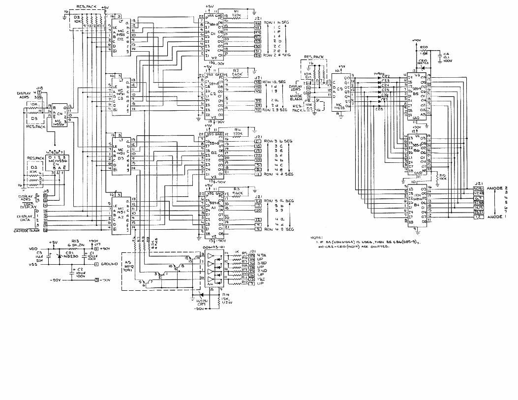
Figure 16: Top View of Score and Match/Credit Display Assembly
Score Panel Removal and Visual Checks
After the +90 volt and -90 volt supply voltages have been verified, the next troubleshooting step on the score panel will be to remove it fromconnector J21.
Turn off AC power to the game, preferably by pulling out the power plug from the wall outlet.1.
Remove the metal clips holding the score panel onto the bracket arms of J21 (refer to Figure 17).WARNING: Glass edges of score panel may be sharp. Use caution to prevent cutting your hands.
2.
Using your right band, grasp the right edge of the score panel. Carefully lift it up approximately 1/4-inch, and then pull it straight outand remove it completely.
3.
Examine the positions of the terminal pins on J21. Tips of the pins should be aligned in the same plane, as shown in the detail view ofFigure 17. If not bent out of alignment, all pins can then make contact with the score panel's terminal strips when the panel is pluggedin.
4.

Next examine the condition of the terminal strips on the score panel. If the surfaces of the strips are corroded, use a pencil eraser toclean them off. Be careful, however, not to rub the eraser against any of the tiny metal ribbons touching certain strips up near the glass(refer to Figure 18). These ribbons must be perfectly centered over the correct pins, not halfway off.
5.
Figure 17: Removal of Score Panel
Figure 18: Score Panel Terminals
Replacement of Score Panel
After the visual checks have been made on the J21 terminal pins and on the score panel the original score panel can be put back, or else a newscore panel can be substituted in its place, Carefully observe the following procedure when replacing the score panel.
Using both hands, grasp tine right-hand edge of the panel and carefully slide it fully into connector J21, perfectly aligned. Then lowerthe edge down until the entire panel rests in the bracket arms. You will note some free space on each side between the panel and thebrackets. At the factory a rubbery substance called RTV was placed between the bracket and the score panel. This substance provides acushion between the glass panel and the metal arms, and positions the panel so that connector J21's terminal pins line up exactly withthe panel's terminal strips. Be sure that they are aligned correctly as shown in Figure 19.
1.
Replace the metal clips that fasten the score panel to the bracket arms.2.

Figure 19: Line-up of Terminal Pins and Terminal Strips
Removing Display Assembly
Certain portions of the PCBs are accessible for troubleshooting when the display assembly is left mounted on the playfield. However, to gainaccess to the remaining portions, or to replace components or an entire PCB, use the following procedure.
Turn off AC power to the game, preferably by pulling out the power plug.1.
Disconnect connectors J17, J18, J19, and J20.2.
Use a Phillips-head screwdriver to loosen the four screws that fasten the display assembly to the playfield, and then remove the screws.3.
Lift the entire assembly up and remove it from the playfield.4.
Installing the Display Assembly
After repair and/or replacement of the display boards and displays, use the following procedure to re-attach the assembly to the playfield.
Lower the assembly down into its final position and line up the four mounting holes with their mating holes in the playfield. Be carefulnot to pinch the lamp wires that are routed through a slot at the lower right corner of the assembly (refer to Figure 20).
1.
Insert the four mounting screws and use a Phillips-head screwdriver to tighten them down.2.
Connect connectors J17, J18, J19, and J20.3.
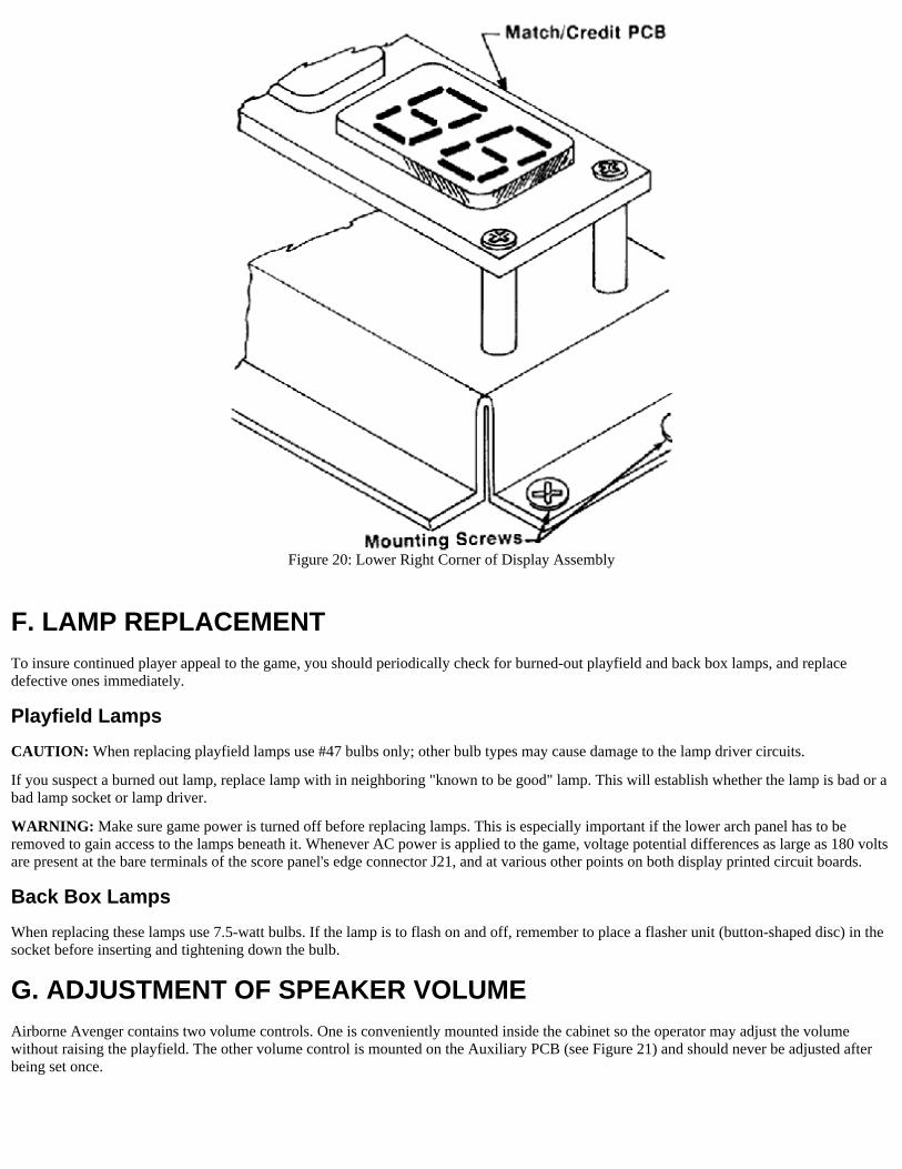
Figure 20: Lower Right Corner of Display Assembly
F. LAMP REPLACEMENTTo insure continued player appeal to the game, you should periodically check for burned-out playfield and back box lamps, and replacedefective ones immediately.
Playfield Lamps
CAUTION: When replacing playfield lamps use #47 bulbs only; other bulb types may cause damage to the lamp driver circuits.
If you suspect a burned out lamp, replace lamp with in neighboring "known to be good" lamp. This will establish whether the lamp is bad or abad lamp socket or lamp driver.
WARNING: Make sure game power is turned off before replacing lamps. This is especially important if the lower arch panel has to beremoved to gain access to the lamps beneath it. Whenever AC power is applied to the game, voltage potential differences as large as 180 voltsare present at the bare terminals of the score panel's edge connector J21, and at various other points on both display printed circuit boards.
Back Box Lamps
When replacing these lamps use 7.5-watt bulbs. If the lamp is to flash on and off, remember to place a flasher unit (button-shaped disc) in thesocket before inserting and tightening down the bulb.
G. ADJUSTMENT OF SPEAKER VOLUMEAirborne Avenger contains two volume controls. One is conveniently mounted inside the cabinet so the operator may adjust the volumewithout raising the playfield. The other volume control is mounted on the Auxiliary PCB (see Figure 21) and should never be adjusted afterbeing set once.
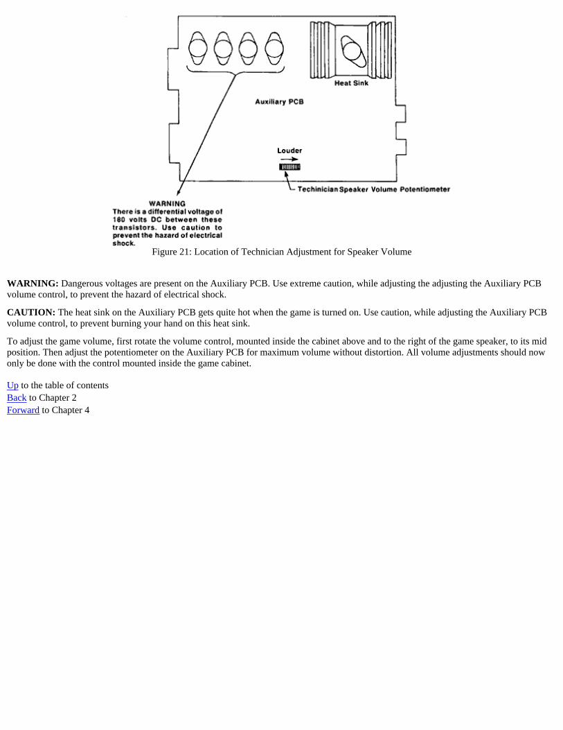
Figure 21: Location of Technician Adjustment for Speaker Volume
WARNING: Dangerous voltages are present on the Auxiliary PCB. Use extreme caution, while adjusting the adjusting the Auxiliary PCBvolume control, to prevent the hazard of electrical shock.
CAUTION: The heat sink on the Auxiliary PCB gets quite hot when the game is turned on. Use caution, while adjusting the Auxiliary PCBvolume control, to prevent burning your hand on this heat sink.
To adjust the game volume, first rotate the volume control, mounted inside the cabinet above and to the right of the game speaker, to its midposition. Then adjust the potentiometer on the Auxiliary PCB for maximum volume without distortion. All volume adjustments should nowonly be done with the control mounted inside the game cabinet.
Up to the table of contentsBack to Chapter 2Forward to Chapter 4

Up to the table of contentsBack to Chapter 3
CHAPTER 4: THEORY OF OPERATION
A. INTRODUCTIONThe block diagram in Figure 22 shows the game's major functional elements and depicts their interconnections. The central element is themicrocomputer, which consists of a microprocessor, memories and control logic.
Figure 22: Functional Block Diagram

By means of a switch sensing circuit, the player operated switches, playfield switches and operator option switches produce switch data forthe microcomputer. Switch closures occur when a player deposits money in the game, depresses the START pushbutton, operates the ballshooter so the ball goes onto the playfield and interacts with playfield objects, and depresses the flipper buttons. Switch Closures also resultwhen a player tilts the game. Executing the instructions stored in the preprogrammed portion of its memory, the microcumpter then respondsto the switch data by energizing various solenoids, lighting various lamps, and producing sound data for the speaker and display data for theScore, Credit and Ball/Match Displays.
B. COMPONENTS OF THE MICROCOMPUTER SYSTEMThe microcomputer system carries out complex tasks of the game by performing a large number of simple tasks. Figure 23 shows a blockdiagram of the microcomputer system and its various interconnecting data, addressing and control buses. The Microprocessing Unit causes thesystem to perform the desired operations by addressing the Program Memory for an instruction (via the Address Bus), reading that instruction(via the bidirectional Data Bus), and then executing the simple task dictated by that instruction. The Microprocessing Unit uses the DataMemory for temporary storage of data necessary for the execution of future instructions, such as arithmetic operations. The MicroprocessingUnit uses the Memory Output Latches for storing the data that is used for producing game sounds energizing solenoids and lighting lamps.

Figure 23: Block Diagram of Microcomputer System
Figure 24: Airborne Avenger Wiring Diagram (2 pages)Click thumbnails for full-sized versions.
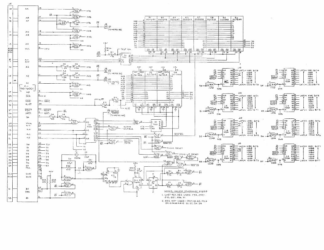
The following paragraphs describe the game's microcomputer system in more detail. The drawing references are to the Processor PCBschematic shown in Figures 25 and 26.
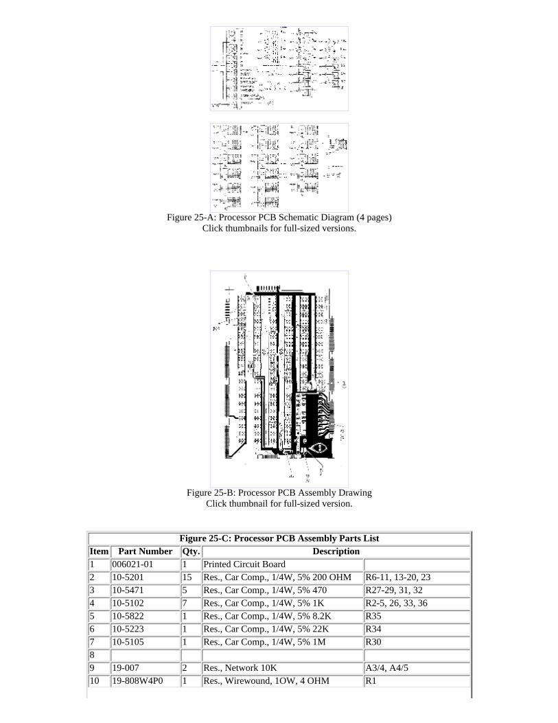
Figure 25-A: Processor PCB Schematic Diagram (4 pages)Click thumbnails for full-sized versions.
Figure 25-B: Processor PCB Assembly DrawingClick thumbnail for full-sized version.
Figure 25-C: Processor PCB Assembly Parts ListItem Part Number Qty. Description1 006021-01 1 Printed Circuit Board 2 10-5201 15 Res., Car Comp., 1/4W, 5% 200 OHM R6-11, 13-20, 233 10-5471 5 Res., Car Comp., 1/4W, 5% 470 R27-29, 31, 324 10-5102 7 Res., Car Comp., 1/4W, 5% 1K R2-5, 26, 33, 365 10-5822 1 Res., Car Comp., 1/4W, 5% 8.2K R356 10-5223 1 Res., Car Comp., 1/4W, 5% 22K R347 10-5105 1 Res., Car Comp., 1/4W, 5% 1M R308 9 19-007 2 Res., Network 10K A3/4, A4/510 19-808W4P0 1 Res., Wirewound, 1OW, 4 OHM R1

11 12 24-250227 1 Cap, Elecrolytic, 220uf, 25V C213 27-250104 27 Cap, Ceramic, 0.1uf, 25V C3, 5, 9-3314 28-101390 3 Cap, Mica, 39pf, 100V C4, 6, 815 28-101151 1 Cap, Mica, 150pf, 100V C716 29-006 1 Cap, Tantalum, 1uf, 35V C117 29-007 1 Cap, Tantalum, 22uf, 15V C3418 19 31-1N914 Diode, 16 1N914 CR2-16, 1920 32-P6KE18 1 Diode, Transient Supp. P6KE18 CR121 34-2N6044 15 Transistor, 2N6044 Q1-8, 11-13, 15-17, 2022 34-2N3643 1 Transistor, 2N3643 Q2123 37-7400 3 I.C. 7400 D10, A1, F124 37-7402 2 I.C. 7402 A2, C725 37-7403 1 I.C. 7403 D926 37-7404 2 I.C. 7404 D4, E1027 37-74L04 1 I.C. 74L04 D1128 37-7407 4 I.C. 7407 D14, D16,D18, D2029 37-7408 3 I.C. 7408 B2, D2, D330 37-74LS08 2 I.C. 74LS08 B/C8, C/D831 37-7414 3 I.C. 7414 B11, C9,E932 37-7420 1 I.C. 7420 B833 37-7427 1 I.C. 7427 B734 37-7432 1 I.C. 7432 C835 37-7437 1 I.C. 7437 C1036 37-7474 2 I.C. 7474 B6, B9
37 37-7493 10 I.C. 7493A6, A7, A8, A9, A10,A11, B3, C11,E12, E13
38 37-74145 8 I.C. 74145F3, F5, F6, F9,F10, F11, F12, F13
39 37-74157 1 I.C. 74157 B540 37-8097 2 I.C. 8097 C4, C541 37-9301 2 I.C. 9301 C6, E1142 37-9316 2 I.C. 9316 B4, D1343 37-9321 1 I.C. 9321 D1
44 37-9334 8 I.C. 9334C13, Cl4, C15, C16,C17, Cl8, Cl9, C20
45 37-9602 1 I.C. 9602 B1046 37-LM323 1 Regulator LM323
47 37-MC1413 10 I.C. MC1413 (2003A)A16, A17, A18, A19, A20,B16, B17, B18, B19, B20
48 37-MC14050 3 I.C. MC14050 A3, A4, A549 50 51 62-001 1 Switch, Push Button SPST 52 66-118P1T 2 Switch, Dip, 8 Position F2, F453 66-12FP1T 1 Switch, Hex 54 72-1608S 2 Screw, Mach., Pan Hd. Phil. #6-32 x 1/2" 55 75-016 2 Washer, Flat #6 56 75-056 2 Washer, Lock, Int. Tooth #6 57 75-916C 2 Nut, Hex #6-32 58 78-06001 1 Heatsink, LM323 59 78-16005 1 Silpad
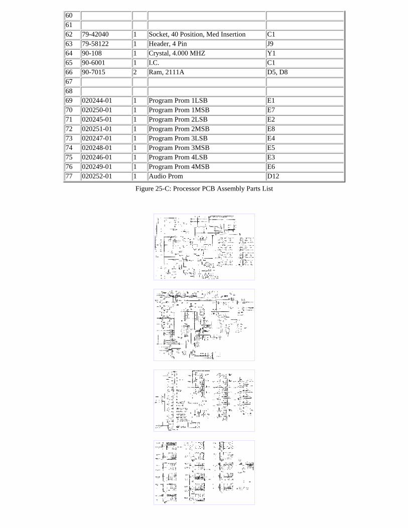
60 61 62 79-42040 1 Socket, 40 Position, Med Insertion C163 79-58122 1 Header, 4 Pin J964 90-108 1 Crystal, 4.000 MHZ Y165 90-6001 1 I.C. C166 90-7015 2 Ram, 2111A D5, D867 68 69 020244-01 1 Program Prom 1LSB E170 020250-01 1 Program Prom 1MSB E771 020245-01 1 Program Prom 2LSB E272 020251-01 1 Program Prom 2MSB E873 020247-01 1 Program Prom 3LSB E474 020248-01 1 Program Prom 3MSB E575 020246-01 1 Program Prom 4LSB E376 020249-01 1 Program Prom 4MSB E677 020252-01 1 Audio Prom D12
Figure 25-C: Processor PCB Assembly Parts List

Figure 26-A: Processor PCB Schematic Diagram (4 pages)Click thumbnail for full-sized version.
Figure 26-B: Processor PCB Assembly DrawingClick thumbnail for full-sized version.
Figure 26-C: Processor PCB Assembly Parts ListItem Part Number Qty. Description1 006021-01 1 Printed Circuit Board 2 10-5201 15 Res., Car Comp., 1/4W, 5% 200 OHM R6-11, 13-20, 233 10-5471 5 Res., Car Comp., 1/4W, 5% 470 R27-29, 31, 324 10-5102 7 Res., Car Comp., 1/4W, 5% 1K R2-5, 26, 33, 365 10-5822 1 Res., Car Comp., 1/4W, 5% 8.2K R356 10-5223 1 Res., Car Comp., 1/4W, 5% 22K R347 10-5105 1 Res., Car Comp., 1/4W, 5% 1M R308 9 19-007 2 Res., Network 10K A3/4, A4/510 19-808W4P0 1 Res., Wirewound, 1OW, 4 OHM R111 12 24-250227 1 Cap, Elecrolytic, 220uf, 25V C213 27-250104 27 Cap, Ceramic, 0.1uf, 25V C3, 5, 9-3314 28-101390 3 Cap, Mica, 39pf, 100V C4, 6, 815 28-101151 1 Cap, Mica, 150pf, 100V C716 29-006 1 Cap, Tantalum, 1uf, 35V C117 29-007 1 Cap, Tantalum, 22uf, 15V C3418 19 31-1N914 Diode, 16 1N914 CR2-16, 1920 32-P6KE18 1 Diode, Transient Supp. P6KE18 CR121 34-2N6044 15 Transistor, 2N6044 Q1-8, 11-13, 15-17, 2022 34-2N3643 1 Transistor, 2N3643 Q2123 37-7400 3 I.C. 7400 D10, A1, F124 37-7402 2 I.C. 7402 A2, C725 37-7403 1 I.C. 7403 D926 37-7404 2 I.C. 7404 D4, E1027 37-74L04 1 I.C. 74L04 D11

28 37-7407 4 I.C. 7407 D14, D16,D18, D2029 37-7408 3 I.C. 7408 B2, D2, D330 37-74LS08 2 I.C. 74LS08 B/C8, C/D831 37-7414 3 I.C. 7414 B11, C9,E932 37-7420 1 I.C. 7420 B833 37-7427 1 I.C. 7427 B734 37-7432 1 I.C. 7432 C835 37-7437 1 I.C. 7437 C1036 37-7474 2 I.C. 7474 B6, B9
37 37-7493 10 I.C. 7493A6, A7, A8, A9, A10,A11, B3, C11,E12, E13
38 37-74145 8 I.C. 74145F3, F5, F6, F9,F10, F11, F12, F13
39 37-74157 1 I.C. 74157 B540 37-8097 2 I.C. 8097 C4, C541 37-9301 2 I.C. 9301 C6, E1142 37-9316 2 I.C. 9316 B4, D1343 37-9321 1 I.C. 9321 D1
44 37-9334 8 I.C. 9334C13, Cl4, C15, C16,C17, Cl8, Cl9, C20
45 37-9602 1 I.C. 9602 B1046 37-LM323 1 Regulator LM323
47 37-MC1413 10 I.C. MC1413 (2003A)A16, A17, A18, A19, A20,B16, B17, B18, B19, B20
48 37-MC14050 3 I.C. MC14050 A3, A4, A549 50 51 62-001 1 Switch, Push Button SPST 52 66-118P1T 2 Switch, Dip, 8 Position F2, F453 66-12FP1T 1 Switch, Hex 54 72-1608S 2 Screw, Mach., Pan Hd. Phil. #6-32 x 1/2" 55 75-016 2 Washer, Flat #6 56 75-056 2 Washer, Lock, Int. Tooth #6 57 75-916C 2 Nut, Hex #6-32 58 78-06001 1 Heatsink, LM323 59 78-16005 1 Silpad 60 61 62 79-42040 1 Socket, 40 Position, Med Insertion C163 79-58122 1 Header, 4 Pin J964 90-108 1 Crystal, 4.000 MHZ Y165 90-6001 1 I.C. C166 90-7015 2 Ram, 2111A D5, D867 68 69 020244-01 1 Program Prom 1LSB E170 020250-01 1 Program Prom 1MSB E771 020245-01 1 Program Prom 2LSB E272 020251-01 1 Program Prom 2MSB E873 020247-01 1 Program Prom 3LSB E474 020248-01 1 Program Prom 3MSB E575 020246-01 1 Program Prom 4LSB E376 020249-01 1 Program Prom 4MSB E6

77 020252-01 1 Audio Prom D1278 79 80 37-74S00 2 I.C. 74S00A F0, F1
Figure 26-C: Processor PCB Assembly Parts List
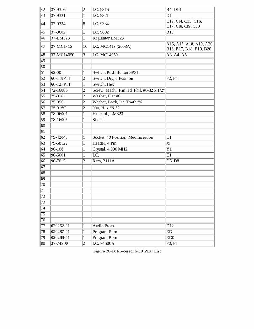
Figure 26-D: Processor PCB Parts ListItem Part Number Qty. Description1 006021-01 1 Printed Circuit Board 2 10-5201 15 Res., Car Comp., 1/4W, 5% 200 OHM R6-11, 13-20, 233 10-5471 5 Res., Car Comp., 1/4W, 5% 470 R27-29, 31, 324 10-5102 7 Res., Car Comp., 1/4W, 5% 1K R2-5, 26, 33, 365 10-5822 1 Res., Car Comp., 1/4W, 5% 8.2K R356 10-5223 1 Res., Car Comp., 1/4W, 5% 22K R347 10-5105 1 Res., Car Comp., 1/4W, 5% 1M R308 9 19-007 2 Res., Network 10K A3/4, A4/510 19-808W4P0 1 Res., Wirewound, 1OW, 4 OHM R111 12 24-250227 1 Cap, Elecrolytic, 220uf, 25V C213 27-250104 27 Cap, Ceramic, 0.1uf, 25V C3, 5, 9-3314 28-101390 3 Cap, Mica, 39pf, 100V C4, 6, 815 28-101151 1 Cap, Mica, 150pf, 100V C716 29-006 1 Cap, Tantalum, 1uf, 35V C117 29-007 1 Cap, Tantalum, 22uf, 15V C3418 19 31-1N914 Diode, 16 1N914 CR2-16, 1920 32-P6KE18 1 Diode, Transient Supp. P6KE18 CR121 34-2N6044 15 Transistor, 2N6044 Q1-8, 11-13, 15-17, 2022 34-2N3643 1 Transistor, 2N3643 Q2123 37-7400 3 I.C. 7400 D10, A1, F124 37-7402 2 I.C. 7402 A2, C725 37-7403 1 I.C. 7403 D926 37-7404 2 I.C. 7404 D4, E1027 37-74L04 1 I.C. 74L04 D1128 37-7407 4 I.C. 7407 D14, D16,D18, D2029 37-7408 3 I.C. 7408 B2, D2, D330 37-74LS08 2 I.C. 74LS08 B/C8, C/D831 37-7414 3 I.C. 7414 B11, C9,E932 37-7420 1 I.C. 7420 B833 37-7427 1 I.C. 7427 B734 37-7432 1 I.C. 7432 C835 37-7437 1 I.C. 7437 C1036 37-7474 2 I.C. 7474 B6, B9
37 37-7493 10 I.C. 7493A6, A7, A8, A9, A10,A11, B3, C11,E12, E13
38 37-74145 8 I.C. 74145F3, F5, F6, F9,F10, F11, F12, F13
39 37-74157 1 I.C. 74157 B540 37-8097 2 I.C. 8097 C4, C541 37-9301 2 I.C. 9301 C6, E11
42 37-9316 2 I.C. 9316 B4, D1343 37-9321 1 I.C. 9321 D1
44 37-9334 8 I.C. 9334C13, Cl4, C15, C16,C17, Cl8, Cl9, C20
45 37-9602 1 I.C. 9602 B1046 37-LM323 1 Regulator LM323
47 37-MC1413 10 I.C. MC1413 (2003A)A16, A17, A18, A19, A20,B16, B17, B18, B19, B20
48 37-MC14050 3 I.C. MC14050 A3, A4, A549 50 51 62-001 1 Switch, Push Button SPST 52 66-118P1T 2 Switch, Dip, 8 Position F2, F453 66-12FP1T 1 Switch, Hex 54 72-1608S 2 Screw, Mach., Pan Hd. Phil. #6-32 x 1/2" 55 75-016 2 Washer, Flat #6 56 75-056 2 Washer, Lock, Int. Tooth #6 57 75-916C 2 Nut, Hex #6-32 58 78-06001 1 Heatsink, LM323 59 78-16005 1 Silpad 60 61 62 79-42040 1 Socket, 40 Position, Med Insertion C163 79-58122 1 Header, 4 Pin J964 90-108 1 Crystal, 4.000 MHZ Y165 90-6001 1 I.C. C166 90-7015 2 Ram, 2111A D5, D867 68 69 70 71 72 73 74 75 76 77 020252-01 1 Audio Prom D1278 020287-01 1 Program Rom ED79 020288-01 1 Program Rom ED080 37-74S00 2 I.C. 74S00A F0, F1
Figure 26-D: Processor PCB Parts List

Figure 27-A: Auxiliary PCB Schematic Diagram (2 pages)Click thumbnails for full-sized versions.
Figure 27-B: Auxiliary PCB Assembly DiagramClick thumbnail for full-sized version.
Figure 27-C: Auxiliary PCB Assembly Parts ListItem Part Number Qty. Description1 006408-01 1 PCB, Blank, Auxiliary Board 2 10-5122 1 Res. CC, 1.2K ohms, 1/4w, 5% R153 10-5152 1 Res. CC, 1.5K ohms, 1/4w, 5% R144 10-5183 2 Res. CC, 18K ohms, 1/4w, 5% R2, 185 10-52P7 1 Res. CC, 2.7 ohms, 1/4w, 5% R106 10-5331 3 Res. CC, 330 ohms, 1/4w, 5% R26, 27, 397 10-5333 3 Res. CC, 33K ohms, 1/4w, 5% R5, 12, 178 10-5683 4 Res. CC, 68K ohms, 1/4w, 5% R3, 16, 30, 319 10-5822 11 Res. CC, 8.2K ohms, 1/4w, 5% R4, 6-9, 13, 19, 42-4510 11-5220 2 Res. CC, 22 ohms, 1/2w, 5% R28, 2911 12-5153 2 Res. CC, 15K ohms, 1w, 5% R24, 2512 13-5390 4 Res. CC, 39 ohms, 2w, 5% R40, 41, 46, 4713 16-5752 2 Resistor, w.w. , 7.5K ohms, 5w, 5% R37, R3814 10-5204 1 Res. CC, 200K, 1/4w, 5% R48

15 19-311502 1 Trimpot, 5000 ohms R116 24-151506 2 Capacitor, Electrolytic,150WVDC, 50ufd C3, C417 24-250106 1 Capacitor, Electrolytic, 25WVDC, 10ufd C518 24-250478 1 Capacitor, Electrolytic, 25WVDC, 4700ufd C119 24-250477 1 Capacitor, Electrolytic, 25WVDC, 470ufd C220 24-250105 1 Capacitor, Electrolytic, 25WVDC, 1.Oufd C621 27-250104 9 Capacitor, Ceramic, 25V, 0.1ufd C7, 9-14, 18, 1922 27-250103 2 Capacitor, Ceramic, 25V, .O1ufd C15, C1623 28-101101 1 Capacitor, Mica, 100V, 100pfd C824 3A-MDA100A 1 Rectifier Assembly, Bridge, MDA100A nbsp;25 31-1N914 1 Diode, 1N914 CR2026 31-1N4005 8 Rectifier, 1N4005 CR10-12, 15-18, 2227 32-P6KE30 1 Transient Suppressor Diode, P6KE30 CR528 32-1N5235 2 Diode, Zener, 1N5235 CR3, CR429 32-1N5242B 1 Diode, Zener, 1N5242B CR1930 32-1N4763A 2 Diode, Zener, 1N4763A CR13, CR1431 33-2N3644 1 Transistor, PNP, 2N3644 Q232 33-2N5883 4 Transistor, PNP, 2N5883 Q6-Q933 34-2N3643 2 Transistor, NPN, 2N3643 Q1, Q1234 34-2N3583 1 Transistor, NPN, 2N3583 Q335 34-2N6044 2 Transistor, NPN, 2N6044 Q10, Q1136 34-2N6282 1 Transistor, NPN, 2N6282 Q537 33-2N6420 1 Transistor, PNP, 2N6420 Q438 37-LM380 1 Integrated Circuit, LM380 D139 37-MC1413 1 Integrated Circuit, MC1413(ULN2003) A140 37-741 1 Integrated Circuit, 741 C141 37-4016 1 Integrated Circuit, 4016 D242 37-7402 2 Integrated Circuit, 7402 A2, A343 37-7407 2 Integrated Circuit, 7407 D3, C244 45 11-5391 1 Resistor, Carbon Comp., 390 ohms, 1/2w, 51% R3546 72-16O8C 10 Screw, Mach., Pan Hd- Phillips, 6-32 x 1/2" Lg. 47 75-016S 10 Washer, Flat, Regular Pattern, #6 48 75-056 10 Washer, Lock, Internal Tooth, #6 49 75-916C 10 Nut, Hex, Regular Pattern, 6-32, Steel 50 12-5103 1 Resistor, Carbon Comp., 10K ohm, 1w, 5% R3651 78-06002 2 Heatsink, Therma1loy #6111B-66 52 79-58123 1 Header, 6-pin, Amp #350431-1 53 79-58124 1 Header, 4-pin, Amp #350761-4 54 78-06012 1 Heatsink, Modified Wakefield #641 55 32-1N6335 1 Diode, Zener, 1N5335 CR156 32-1N5230 1 Diode, Zener, 1N5230 CR2157 10-5101 1 Resistor, Carbon Comp., 100 ohms, 1/4w, 5% R1158 59 78-16011 2 Silpad, TO-66 60 72-1408C 4 Screw, Mach, Pan Hd Phil., #4-40 x 1/2 Cres 61 75-014S 4 Washer, Flat, Reg Pattern #4 62 75-054 4 Washer, Lock, Int. Tooth #4 63 75-914C 4 Nut, Hex, Reg Pattern #4-40 Cres 64 75-09012 4 Washer, Shoulder 65 78-OA01 2 Cover, Insulating, to-66 Q10, 1166

67 10-5221 1 Res., C.C. 220 Ohms, 1/4w, 5% R3368 75-09015 3 Shoulder Washer (Seastrom 5605-25) 69 10-5201 2 Res., C.C., 200 Ohms, 1/2w 5% R21, 22
Figure 27-C: Auxiliary PCB Assembly Parts List
On the schematic the symbol P (which appears at various inputs to logic gates and other integrated circuits) indicates a connection to +5 voltsthrough a pull-up resistor.
As an aid for locating integrated circuit devices referred to in the schematics and assembly drawings, and on the boards themselves, each ICposition is given a letter/number designation. On the PCB the IC devices are arranged in columns (along the short dimension of the board) androws (along the long dimension). The letter refers to a column, and the number refers to a row.
Thus, for example, the type-9321 IC device given the designation D1 and drawn near the center of sheet 1 is found as the second device in the"D" row of devices mounted on that board.
Microprocessing unit
The large block drawn along the left side of sheet 1 of the schematic represents the Microprocessing Unit. The signal names for the variousData Bus, Address Bus and Processor Controls are labeled inside the block.
Program Memory
Eight ROM devices in locations E1 through E8 for the -08 PCB and two ROM devices in locations E00 and E0 for the -09 PCB form theprogram memory. Note that the address inputs of all ROMs are connected in parallel and are tied to the A0B through A9B signals. Thesesignals are produced by buffer logic connected to the Microprocessing Unit's Address Bus (signals AO through A9). Also note that all CE2inputs (pin 10) are tied together and driven by a common signal, and that the CE1 inputs are driven by signals derived from A10 and A11produced by the Microprocessing Unit. All ROM data terminals are connected in parallel to the Data Bus (DO through D7).
Although all eight devices are ROMs, they should never be interchanged (that is, E1 unplugged and plugged into the E2 position, and viceversa), because different data has been programmed in each ROM.
Inside each ROM the data is organized in a 1K x 4 format (1024 bits by 4), giving each ROM a capacity of 4096 data bits.
Data Memory
The four devices in locations D5 through D8 form the Data Memory. Note that all address inputs are connected in parallel (together with theROMs) to the A0B through A9B signals, and that all RAM data terminals are connected in parallel (together with the ROMs) to the Data Bus.The Microprocessing Unit's R/W bus control signal is buffered and then connected to all RAM R/W inputs.
Memory Output Latches
The eight type-9334 devices along the right side of the sheet form the Memory Output Latches. The addressing signals applied to each latch(at pins 1, 2, and 3) are derived from the A2, A3, and A7 Address Bus signals. One Data Bus bit is applied to each latch device (for example,Bit DO is applied to the latch in location C20, Bit D1 to C19, and so forth). The ^REG LD^ (Register Load) signal, produced by the ControlLogic, is applied to the ^E^ (Enable not) input of every latch device (at pin 14).
Editor's note: ^THIS^ notation will be used to indicate a horizonal line over words; this is impossible to show in HTML.
Each latch device has eight outputs, giving a total of 64 LATCH signals. Twelve of these (the signals LATCH 1080 BIT 0 through 4, LATCH1084 BIT 0 through 4, and Latch 1084 BIT 0 through 4), provide the Sound Data, 32 provide the Lamp Data, and the remaining 20 providethe Solenoid Data.
Clock Generator
The circuit is shown along the bottom of the sheet. The basic frequency source is a 4-MHz crystal-controlled oscillator. Its output is thenshaped, divided down, and buffered to produce the ^(PHI)1^ and ^(PHI)2^ signals (phase 1 not and phase 2 not). These are thenon-overlapping, non-symmetrical square wave complements required by the Microprocessing Unit. They are also used in the Control Logic.
Tri-State Buffers
The two type-8097 devices in locations C4 and C5 on sheet 2 connect Switch Data, power line phasing information, display addressinformation, and other Control Logic signals to bits D6 and D7 of the Data Bus, and to Bits A0 through A5 and A12 through A14 of the

Address Bus. Keep in mind that these are Tri-State devices. When its control line is in the disable state, a tri-state device's data connectionsbecome a high impedance, the equivalent of removing the device from the circuit. But when the control line is in the enable state, the device'sdata connections are capable of having normal high and low ("1" and "0") levels.
Control Logic
The portion of the Control Logic that produces the ^RESET^ signal for the Microprocessing Unit is shown at the top of sheet 2. The fivetype-7493 Counter devices form a single, simple binary counter configuration that is driven by the phase 1 clock signal. The AUDIO CLOCKsignal produced by the first 7493 device (at A6 pin 8) is used in the Sound Generator circuit.
If, at any time after power is applied to the game, the count advances far enough to bring the last stage high (A10 pin 9 high), then the^RESET^ signal will be brought low. (^RESET^ can also be brought low by manually depressing the ^RESET^ pushbutton mounted onthe surface of the Processor PCB.) ^RESET^ going low causes the Microprocessing Unit to begin the restart sequence. The execution of aroutine to initialize the processor from its reset condition will be started.
In normal game operation the ^RESET^ signal stays low. The WAKE-UP RESET signal (applied at pins 2 and 3 of both A9 and A10)periodically goes high, preventing the last counter stages from going high. If some abnormal circumstance occurs, such as a momentaryinterruption in game power caused by severe transients on the AC power line, then the program sequence inside the Microprocessing Unitmay be disrupted and the WAKE-UP RESET signal may remain low for longer than 100 milliseconds. In such a case, a high-to-low-leveltransition (positive-going edge) on the ^RESET^ signal is produced, and the microcomputer system resets itself.
Other portions of the Control Logic are covered under the Circuit Descriptions that follow.
C. CIRCUIT DESCRIPTIONS
Solenold Driver Circuits
Twenty of the outputs from the Memory Output Latches constitute the Solenoid Data shown in Figure 23. These are the signals LATC 1080BIT 4 through 7, LATCH 1084 BIT 4 through 7, LATCH 1088 BIT 4 through 7, and LATCH 108C BIT 0 through 7 (shown on sheet 1 ofProcessor PCB schematic).
Two of these signals, LATCH 1080 BIT 4 and 5, connect to the Auxiliary PCB where they each drive a type-7407 Inverter followed by a2N6044 Darlington- connected transistor pair. The remaining eighteen LATCH signals connect to the same types of devices (7404 and2N6044) on the Processor PCB.
Figure 30 shows a simplified diagram of the basic solenoid drive circuit for all solenoids. One side of the solenoid coils connects to thecollectors of the 2N6044 transistors; the other side is brought, together with all the other coils, to an unregulated, full-wave rectified DCpower supply of about 35 volts amplitude. This power supply is located in the Power Supply Assembly in the right rear corner of the cabinet.Note that a suppression diode is placed across each coil; the diode protects the 2N6044 from reverse inductive kickback (back emf) when thecoil is de-energized. The emitters of all 2N6044 devices and the ground side of the 35-volt supply are returned to SOLENOID GRD (at J9, pin3).

Figure 30: Simplified Diagram of Basic Solenoid Driver Circuit
Remember that the microcomputer, by means of the PHASE signal, is able to synchronize the turning on of the solenoids so that it will startonly at a zero crossing point (zero power point) of the power line waveform.
Drive components for the coin counter metering function are on the Processor PCB. Also provided are signals from the microcomputer andspaces on the board for additional drive components, so that operators wishing to have four additional functions can do so by installingadditional components. The four functions, components required, and their circuit designations are listed in Table 15. Figure 31 shows thecircuit for each metering function to be added.
Table 15: Components Required for Special Metering Functions(Available at edge connector J-8 on the main processor PCB)
Function Being Metered Processor PCBEdge Connector J8 Pin
2N6044Driver Number
1N914Designation
ResistorDesignation
Total replays X, 20 10 CR20 R25Total specials awarded U, 17 19 CR17 R21Total game time (min.) V, 18 9 CR18 R24Total plays W, 19 20 CR19 R23

Figure 31: Additional Components to be Installed for Each Metering Function Added
Lamp Driver Circuits
Thirty-two of the outputs from the Memory Output Latches constitute the lamp data shown in Figure 23. These are the BIT 0 through BIT 7signals LATCH 1000, LATCH 1004, LATCH 1008 and LATCH 100C. All thirty-two signals connect to the inputs of the type ULN-2003Adevices shown on sheet 4 of the Processor PCB schematic. These are open-collector interface devices that accept TTL input levels, andproduce the high current outputs needed to light the lamps. Note that these devices connect to a lamp ground (J19, pin 3).
Figure 32 shows a simplified diagram of the basic lamp driver circuit. One side of each lamp connects to a ULN-2003A output terminal, andthe other side connects to a strobe line on the Auxiliary PCB (STROBE A, STROBE B, etc.). In the wiring harness, beneath the playfield,black wires are used for lamps connecting to STROBE A, green wires for those to STROBE B, blue wires for STROBE C, and red wires forSTROBE D.

Figure 32: Simplified Diagram of Basic Lamp Driver Circuit
The control logic decodes the LAMP BIT 0 and LAMP BIT 1 signals to produce four transistor based drive signals, one for each 2N5883.(LAMP BIT 0 and LAMP BIT 1 come from the same circuit that produces the DISPLAY ADRS 1 and DISPLAY ADRS 2 signals on theProcessor PCB schematic.) The timing of the four signals driving the 2N5883 transistors is such that any one transistor is brought intoconduction only 25% of the time (25% duty cycle), This means that the playfield lamps, which appear to the eye to be of uniform brightnesswhen lighted, are in reality blinking on and off.
CAUTION: During troubleshooting of the game by service technicians, while operating the game with the cabinet open and power applied,do not hold down the RESET pushbutton (mounted on the Processor PCB) for long periods of time. Doing this will cause one of the 2N5883transistors to be brought into conduction 100% of the time. Lamp current is very high in this situation, and can lead to premature burning outof the lamps.
Switch Sensing Circuit
The switch sensing circuit accepts switch closure information as an input, and produces switch data as an output. This switch data is sent tothe microcomputer system on a single signal line. Figure 33 shows a simplified diagram of the switch sensing circuit.

Figure 33: Simplified Diagram of Switch Sensing Circuit
The normally open (NO contacts) of the various playfield switches and certain cabinet switches are connected together in the playfield harnesswiring, and then a common lead is brought to the Processor PCB at connector J7 (pins 5 & 6). (Refer to sheet 2 of the Processor PCBschematic.) On the board's artwork, the NO contacts from the Operator Option Switches (along with signals derived from the rest of thecabinet switches -- COIN 1, COIN 2, START, and SLAM), are also connected electronically to this point. Also, this point is connected toresistor R27, tied to +5 volts, and to the pin-13 input of the type-7414 Inverter in location C9. The output of this Inverter, C9 pin 12, is theSwitch Data line, which is applied to pin 12 of the type-8097 tri-state buffer in location C5. The device terminal at C5 pin 11 is connected tobit D7 of the Microprocessing Unit's bidirectional Data Bus.
By means of multiplexing technique, the switch closure information being sent on the switch data line is derived from the timing of addressingsignals being sent out by the Microprocessing Unit over the Address Bus. To determine whether or not a specific switch is closed, theMicroprocessing Unit compares the timing of that switch's address code with the state of the switch data signal being received at that momenton bit D7 of the data bus.
Figure 34 shows simplified wave form diagrams that illustrate this timing comparison multiplex technique for an imaginary circuit havingonly eleven switches.

Figure 34: Simplified Diagram of Switch Censing Circuit Waveforms
In the actual game, anytime that the Microprocessing Unit addresses a specific switch, and that switch is closed at that moment, the SWITCHCOMMON line will be low. The 7414 Inverter changes this to high, and a high goes out on the Data Bus on bit D7. So when theMicroprocessing Unit reads back a high in that location on the data bus, it knows that the specific switch had been closed.
The control logic used for decoding the Microprocessing Unit's addressing information is shown on the left side of sheet 3 of the schematic.One SWITCH DECODE line is produced for each switch (switch DECODE 200B, SWITCH DECODE 200A, etc.).
Displays and Display Data
The Score Display consists of a glass plate panel that plugs into an edge connector, and a printed circuit board beneath that plugs into a secondconnector. The two connectors are hard-wired together. The Credit and Ball/Match displays are both built on a separate PCB.
WARNING: Whenever AC power is applied to the game, voltage potential differences as large as 180 volts are present at the bare terminalsof the glass plate's edge connector, and at various other points on both printed circuit boards.
All three are gas-discharge type displays with the following principle of operation. If a sufficiently high voltage is applied to a gas, a pointwill be reached at which the gas ionizes, producing a conduction current and giving off radiation (which can be in the form of visible light).Fluorescent lamps are common examples of illumination sources that also make use of the gas-discharge phenomenon.
A display segment lights up when +90 volts is applied to the anode at the same time that -90 volts is applied to the cathode, as illustrated bythe waveforms in Figure 35.
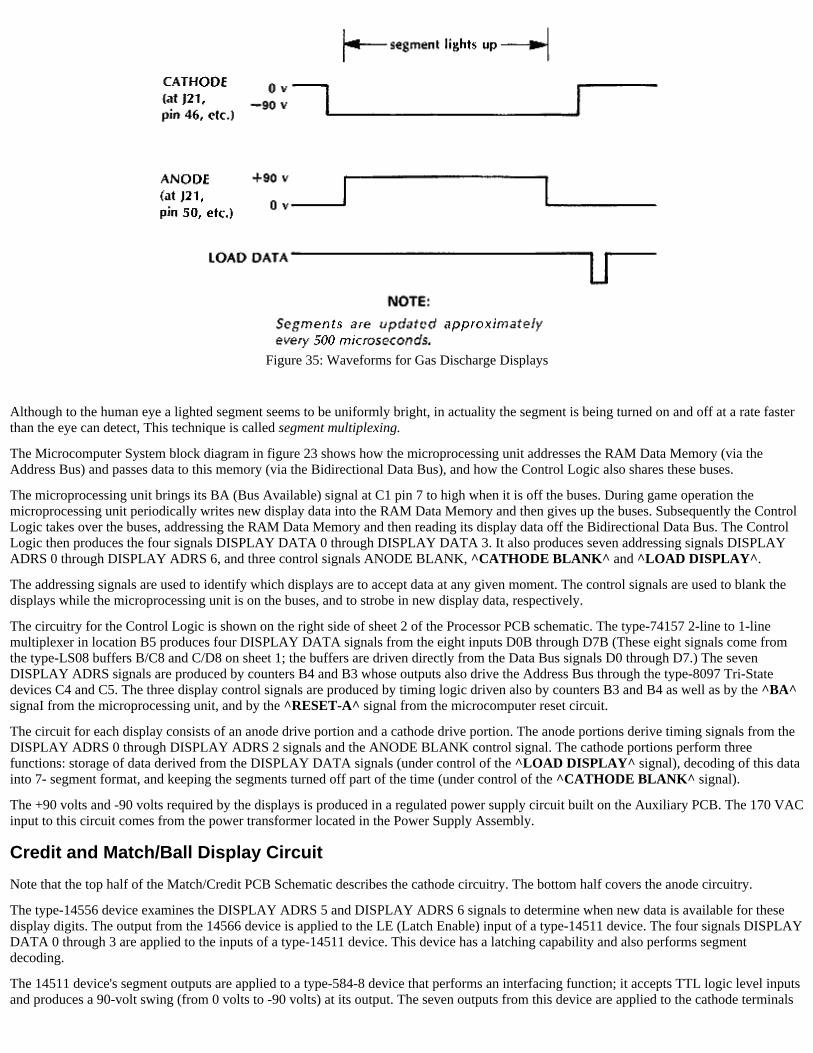
Figure 35: Waveforms for Gas Discharge Displays
Although to the human eye a lighted segment seems to be uniformly bright, in actuality the segment is being turned on and off at a rate fasterthan the eye can detect, This technique is called segment multiplexing.
The Microcomputer System block diagram in figure 23 shows how the microprocessing unit addresses the RAM Data Memory (via theAddress Bus) and passes data to this memory (via the Bidirectional Data Bus), and how the Control Logic also shares these buses.
The microprocessing unit brings its BA (Bus Available) signal at C1 pin 7 to high when it is off the buses. During game operation themicroprocessing unit periodically writes new display data into the RAM Data Memory and then gives up the buses. Subsequently the ControlLogic takes over the buses, addressing the RAM Data Memory and then reading its display data off the Bidirectional Data Bus. The ControlLogic then produces the four signals DISPLAY DATA 0 through DISPLAY DATA 3. It also produces seven addressing signals DISPLAYADRS 0 through DISPLAY ADRS 6, and three control signals ANODE BLANK, ^CATHODE BLANK^ and ^LOAD DISPLAY^.
The addressing signals are used to identify which displays are to accept data at any given moment. The control signals are used to blank thedisplays while the microprocessing unit is on the buses, and to strobe in new display data, respectively.
The circuitry for the Control Logic is shown on the right side of sheet 2 of the Processor PCB schematic. The type-74157 2-line to 1-linemultiplexer in location B5 produces four DISPLAY DATA signals from the eight inputs D0B through D7B (These eight signals come fromthe type-LS08 buffers B/C8 and C/D8 on sheet 1; the buffers are driven directly from the Data Bus signals D0 through D7.) The sevenDISPLAY ADRS signals are produced by counters B4 and B3 whose outputs also drive the Address Bus through the type-8097 Tri-Statedevices C4 and C5. The three display control signals are produced by timing logic driven also by counters B3 and B4 as well as by the ^BA^signaI from the microprocessing unit, and by the ^RESET-A^ signal from the microcomputer reset circuit.
The circuit for each display consists of an anode drive portion and a cathode drive portion. The anode portions derive timing signals from theDISPLAY ADRS 0 through DISPLAY ADRS 2 signals and the ANODE BLANK control signal. The cathode portions perform threefunctions: storage of data derived from the DISPLAY DATA signals (under control of the ^LOAD DISPLAY^ signal), decoding of this datainto 7- segment format, and keeping the segments turned off part of the time (under control of the ^CATHODE BLANK^ signal).
The +90 volts and -90 volts required by the displays is produced in a regulated power supply circuit built on the Auxiliary PCB. The 170 VACinput to this circuit comes from the power transformer located in the Power Supply Assembly.
Credit and Match/Ball Display Circuit
Note that the top half of the Match/Credit PCB Schematic describes the cathode circuitry. The bottom half covers the anode circuitry.
The type-14556 device examines the DISPLAY ADRS 5 and DISPLAY ADRS 6 signals to determine when new data is available for thesedisplay digits. The output from the 14566 device is applied to the LE (Latch Enable) input of a type-14511 device. The four signals DISPLAYDATA 0 through 3 are applied to the inputs of a type-14511 device. This device has a latching capability and also performs segmentdecoding.
The 14511 device's segment outputs are applied to a type-584-8 device that performs an interfacing function; it accepts TTL logic level inputsand produces a 90-volt swing (from 0 volts to -90 volts) at its output. The seven outputs from this device are applied to the cathode terminals

of all display segments. The CATHODE BLANK signal, applied to the B1 input (pin 4 of the 14511 device), will cause all segments to beblank, regardless of what data is stored, when the multiplex timing calls for that digit to remain unlighted.
The Type-14028 device, in the anode portion of the circuit, examines the three signals DISPLAY ADRS 0 through 2 to determine which ofthe display digits to turn on. The outputs from the 14028 are applied through series-connected diodes to a type-585-6 interface device thatdrives the anode terminals of the display digits with a voltage swing from 0 volts to +90 volts.
Figure 29-A: Match/Credit PCB Schematic Diagram

Figure 29-B: Match/Credit PCB Assembly Drawing
Figure 29-C: Match/Credit PCB Assembly Parts ListItem Part Number Description1 006104-01 1 PCB, Blank, Match/Credit Display Board 2 10-5155 2 Resistor, Carbon Comp., 1.5 Megohms, 1/4w, 5% R3, 43 10-5394 1 Resistor, Carbon Comp., 390K ohms, 1/4w, 5% R24 12-5103 1 Resistor, Carbon Comp., 10K ohms, 1w, 5% R15 24-500105 1 Capacitor, Electrolytic, 50 WVDC, 1.0 ufd C36 7 24-101106 2 Capacitor, Electrolytic, 100 WVDC, 10 ufd C1, 28 32-1N5230 1 Diode, Zener, 1N5230 CR19 37-MC14028 1 Integrated Circuit, MC14028 10 37-MC14511 1 Integrated Circuit, MC14511 11 37-MC14556 1 Integrated Circuit, MC14556 12 37-584-8 1 Integrated Circuit, 584-8 13 37-585-6 1 Integrated Circuit, 585-6 14 19-008 1 Resistor Network, 10K ohms, CTS#761-1-R10K 15 31-1N914 4 Diode, 1N914 CR2-516 79-41001 2 Socket, Beckman Type CS-352 17 10-5104 1 Res, Carbon Comp., 100K, 1/4W, 5% R518 32-1N4744 1 Diode, Zener 1N4744 CR6
Figure 29-C: Match/Credit PCB Assembly Parts List

Score Display Circuit
The connections to the score display panel are made in the form of a rectangular matrix, with seven anode connections on one side and 28cathode connections on the other. Figure 36 illustrates the arrangement of these connections. In the multiplex timing the six vertical rows ofdigits, plus the one vertical row of player up indications, are driven one at a a time. All the anodes in the player up indications are broughttogether electrically to J21, pins 1 and 2, the ANODE 1 signal, All the anodes for the least significant digits are brought to J21, pins 50 and 5,the ANODE 2 signal, etc. The sequence of lighting the anodes is: ANODE 2, then 4, then 6, then 3, then 5, then 7, and finally ANODE 1.
Likewise, the cathodes of all segments of the digits in a row are tied together, For example, all the "b" segments in the top row are tiedtogether and brought to J21, pin 46.
Figure 36: Arrangement of Connections to Score Panel

For the circuit descriptions that follow, refer to the schematic in Figure 28. The four display address signals (DISPLAY ADRS 3 through 6)are applied to type-14556 devices which produce four outputs. One of these outputs is applied to the LE input (pin 5) of each of thetype-14511 Latch/Segment Decoder devices in locations D2, C3, B3, and A2. The 14556 devices decide which of the Latch/SegmentDecoders are to receive display data (are to be loaded) at any one moment.
Figure 28-A: Score Panel Drive PCB Schematic DiagramClick thumbnail for full-sized version.
Figure 28-B: Score Panel Drive PCB Assembly DrawingClick thumbnail for full-sized version.
Figure 28-C: Score Panel Drive PCB Assembly ListItem Part Number Qty. Description1 004922-01 1 PCB, Blank, Score Panel Drive 2 10-5102 8 Res., Carbon Comp., 1000 ohms, 1/4w, 5% R5-123 10-5224 2 Res., Carbon Comp , 220K, ohms, 1/4w, 5% R1, 44 10-5564 2 Res., Carbon Comp., 560K ohms, 1/4w, 5% R2, 35 10-5822 4 Res., Carbon Comp., 8200 ohms, 1/4w, 5% R16-196 11-5153 1 Res., Carbon Comp., 15K ohms, 1/2w, 5% R147 13-5682 1 Res., Carbon Comp., 6800 ohms, 2w, 5% R138 24-101106 2 Capacitor, Electrolytic, 100WVDC. 10ufd C1-29 24-500105 1 Capacitor, Electrolytic, 50WVDC, 1.0ufd C310 32-1N4751 1 Diode, Zener, 1N4751 CR911 32-1N5230 1 Diode, Zener, 1N5230 CR112 19-008 1 Res. Network, 1OK ohms, CTS# 761-1-R10K 13 37-MC14028 1 Integrated Circuit, MC14028 14 37-MC14511 4 Integrated Circuit, MC14511 15 37-MC14556 1 Integrated Circuit, MC 14556 16 37-MPQ7091 1 Integrated Circuit, MPQ7091 17 37-UDN6184A 1 Integrated Circuit, UDN6184A 18 37-584-8 4 Integrated Circuit, 584-8 19 006123-01 1 Integrated Circuit, MC1413, 75V (Atari Custom) 20 004770-01 1 Connector, Score Panel

21 72-1408S 4 Screw, Mach., Pan Hd., Phil., 4-40 x 1/2" Lg., Stl 22 10-5104 1 Res., Car Comp., 100K ohms 5% R1523 32-1N4744 1 Diode, Zener 1N4744 CR1024 10-5382 1 Res. Car Comp., 1.8K ohms 1/2w, 5% R2025 27-10104 1 Capacitor, Ceramic Disc 0.1uf 100V C4NOTE: This is the preferred assembly parts lists for the Score Display PCB, to be used when item 17 is obtainable. If item 17 is unavailable(only) use the assembly parts list, A004924-02 as an alternate procedure.
Figure 28C: Score Panel Drive PCB Assembly Parts List
The individual segment outputs ("a" through "g") produced by the segment decoders are applied to four type-584-8 Cathode Driver devices inlocations D1, C2, B2, and A1. These Cathode Drivers perform an interfacing function; they accept TTL logic level inputs and they produce a90-volt swing (from 0 volts to -90 volts) at their outputs. A separate circuit (formed by four 8.2K-ohm resistors, a 4-transistor MPQ 7091device in location A5, and the 006123-01 device in A4), produces the signals applied to the "Player Up" cathodes (4TH UP 3RD UP, etc.)
The circuitry for driving the anodes of the display is shown on the right half of the sheet. The type-14028 device examines the DISPLAYADR 0 through 2 signals to determine which of the seven ANODE lines are to be turned on. The outputs of the 14028 are applied to interfacedevice or devices that will produce the 90-volt swing (from 0 volts to +90 volts) at their outputs. This PCB is laid out in such a way that twochoices of device type are possible. (A board will be built using only one choice.) The choices are: one type-UDN 6184A device, or twotype-585-9 devices.
Sound Generator and Speaker Driver Circuits
The initial portion of the Sound Generator circuit is built on the Processor PCB. The final portion and the Speaker Driver are built on theAuxiliary PCB. In the lower left corner of sheet 2 of the Processor PCB schematic, four Memory Output Latch signals (LATCH 1088 Bit 0through LATCH 1088 Bit 3) are applied to the type-9316 counter in location D13. This counter is driven by the AUDIO CLOCK signal andserves as a frequency generator. The counter's TC (terminal count) output (at D13 pin 15) is applied to a second counter configuration formedby two type-7493 counter devices. The AUDIO ENABLE and AUDIO RESET signals (produced by Control Logic section shown onschematic sheet 1) are applied to the R01 and R02 reset inputs of these counters (pins 2 and 3). These two signals control when the Same'ssound is allowed to come on and when it is kept off.
Five output signals from the 7493 counters, together with four more Memory Output Latch signals (LATCH 1080 BIT 0 through BIT 3), areapplied to the address inputs of the ROM device in location D12. This ROM has been pre-programmed to perform a waveform shapingfunction. The ROM outputs, AUDIO 0 through AUDIO 3, are sent to the Auxiliary PCB.
On the Auxiliary PCB schematic these four AUDIO signals are connected to type-7407 open-collector buffers. The buffer outputs connect, viaa "weighted" resistor network, to the pin 3 positive input of the amplifier in location C1. The network is called "weighted" because of thebinary-weighted values of the resistors; 68K ohms is double the value of the 33K-ohms resistor which is double the value of the 18K-ohmresistor, etc. This weighted resistor-buffer arrangement performs a D-to-A (digital to analog) converter function. Note that other resistors, a1.5K-ohm to ground and a 1.2K-ohm that connects to +13.6 volts, are also tied into this resistor network.
Four more Memory Output Latch signals (LATCH 1084 BIT 0 through BIT 3) are applied to the Auxiliary PCB. After buffering by type-7407devices, these signals are applied to the gate inputs (pins 5, 6, 12, and 13) of the type-4016 Quad CMOS Analog Switch in location D2. Thesefour latch outputs provide the amplitude modulation information portion of the Sound Data. The outputs of the type-4016 Analog Switchconnect, via another "weighted" resistor network, to the negative input (pin 2) of amplifier C1. Thus the 4016 device provides amplitude orgain control for the amplifier. Amplifier C1 acts as a mixer stage for all the Sound Data, and its output (at C1 pin 6) is applied to the SpeakerDrive circuit.
The LM380 amplifier in location D1 serves as the Speaker Driver. Potentiometer R1 provides the game's first speaker volume adjustment. TheLM380 output at D1 pin 8 connects, via harness wiring, to the second speaker volume potentiometer. This potentiometer is located underneaththe cabinet at the front left corner. The wiper of the potentiometer connects directly to the game speaker.
End of Manual
Up to the table of contentsBack to Chapter 3